KR101370650B1 - Switch contoller, a control method of the switch, the converter, and the driving method using the switch contoller and the control method of the switch - Google Patents
Switch contoller, a control method of the switch, the converter, and the driving method using the switch contoller and the control method of the switch Download PDFInfo
- Publication number
- KR101370650B1 KR101370650B1 KR1020070040242A KR20070040242A KR101370650B1 KR 101370650 B1 KR101370650 B1 KR 101370650B1 KR 1020070040242 A KR1020070040242 A KR 1020070040242A KR 20070040242 A KR20070040242 A KR 20070040242A KR 101370650 B1 KR101370650 B1 KR 101370650B1
- Authority
- KR
- South Korea
- Prior art keywords
- voltage
- signal
- soft start
- feedback
- switch
- Prior art date
- Legal status (The legal status is an assumption and is not a legal conclusion. Google has not performed a legal analysis and makes no representation as to the accuracy of the status listed.)
- Active
Links
- 238000000034 method Methods 0.000 title claims abstract description 90
- 239000003990 capacitor Substances 0.000 claims description 67
- 238000001514 detection method Methods 0.000 claims description 44
- 230000007423 decrease Effects 0.000 claims description 34
- 230000007274 generation of a signal involved in cell-cell signaling Effects 0.000 claims description 4
- 230000003247 decreasing effect Effects 0.000 claims description 3
- 238000010586 diagram Methods 0.000 description 19
- 101100508411 Caenorhabditis elegans ifb-1 gene Proteins 0.000 description 10
- 101100508412 Caenorhabditis elegans ifb-2 gene Proteins 0.000 description 9
- 230000000903 blocking effect Effects 0.000 description 9
- 230000000630 rising effect Effects 0.000 description 3
- 230000005669 field effect Effects 0.000 description 2
- 230000007257 malfunction Effects 0.000 description 2
- 229910044991 metal oxide Inorganic materials 0.000 description 2
- 150000004706 metal oxides Chemical class 0.000 description 2
- 238000010606 normalization Methods 0.000 description 2
- 239000004065 semiconductor Substances 0.000 description 2
- 238000009499 grossing Methods 0.000 description 1
- 238000004519 manufacturing process Methods 0.000 description 1
- 238000012986 modification Methods 0.000 description 1
- 230000004048 modification Effects 0.000 description 1
- 238000005070 sampling Methods 0.000 description 1
Images


Classifications
-
- H—ELECTRICITY
- H02—GENERATION; CONVERSION OR DISTRIBUTION OF ELECTRIC POWER
- H02M—APPARATUS FOR CONVERSION BETWEEN AC AND AC, BETWEEN AC AND DC, OR BETWEEN DC AND DC, AND FOR USE WITH MAINS OR SIMILAR POWER SUPPLY SYSTEMS; CONVERSION OF DC OR AC INPUT POWER INTO SURGE OUTPUT POWER; CONTROL OR REGULATION THEREOF
- H02M3/00—Conversion of DC power input into DC power output
- H02M3/22—Conversion of DC power input into DC power output with intermediate conversion into AC
- H02M3/24—Conversion of DC power input into DC power output with intermediate conversion into AC by static converters
- H02M3/28—Conversion of DC power input into DC power output with intermediate conversion into AC by static converters using discharge tubes with control electrode or semiconductor devices with control electrode to produce the intermediate AC
- H02M3/325—Conversion of DC power input into DC power output with intermediate conversion into AC by static converters using discharge tubes with control electrode or semiconductor devices with control electrode to produce the intermediate AC using devices of a triode or a transistor type requiring continuous application of a control signal
- H02M3/335—Conversion of DC power input into DC power output with intermediate conversion into AC by static converters using discharge tubes with control electrode or semiconductor devices with control electrode to produce the intermediate AC using devices of a triode or a transistor type requiring continuous application of a control signal using semiconductor devices only
- H02M3/33507—Conversion of DC power input into DC power output with intermediate conversion into AC by static converters using discharge tubes with control electrode or semiconductor devices with control electrode to produce the intermediate AC using devices of a triode or a transistor type requiring continuous application of a control signal using semiconductor devices only with automatic control of the output voltage or current, e.g. flyback converters
- H02M3/33523—Conversion of DC power input into DC power output with intermediate conversion into AC by static converters using discharge tubes with control electrode or semiconductor devices with control electrode to produce the intermediate AC using devices of a triode or a transistor type requiring continuous application of a control signal using semiconductor devices only with automatic control of the output voltage or current, e.g. flyback converters with galvanic isolation between input and output of both the power stage and the feedback loop
-
- H—ELECTRICITY
- H02—GENERATION; CONVERSION OR DISTRIBUTION OF ELECTRIC POWER
- H02M—APPARATUS FOR CONVERSION BETWEEN AC AND AC, BETWEEN AC AND DC, OR BETWEEN DC AND DC, AND FOR USE WITH MAINS OR SIMILAR POWER SUPPLY SYSTEMS; CONVERSION OF DC OR AC INPUT POWER INTO SURGE OUTPUT POWER; CONTROL OR REGULATION THEREOF
- H02M1/00—Details of apparatus for conversion
- H02M1/36—Means for starting or stopping converters
-
- Y—GENERAL TAGGING OF NEW TECHNOLOGICAL DEVELOPMENTS; GENERAL TAGGING OF CROSS-SECTIONAL TECHNOLOGIES SPANNING OVER SEVERAL SECTIONS OF THE IPC; TECHNICAL SUBJECTS COVERED BY FORMER USPC CROSS-REFERENCE ART COLLECTIONS [XRACs] AND DIGESTS
- Y10—TECHNICAL SUBJECTS COVERED BY FORMER USPC
- Y10S—TECHNICAL SUBJECTS COVERED BY FORMER USPC CROSS-REFERENCE ART COLLECTIONS [XRACs] AND DIGESTS
- Y10S323/00—Electricity: power supply or regulation systems
- Y10S323/901—Starting circuits
Landscapes
- Engineering & Computer Science (AREA)
- Power Engineering (AREA)
- Dc-Dc Converters (AREA)
Abstract
본 발명은 스위치 제어 장치, 스위치 제어 방법, 및 이를 이용하는 컨버터 및 그 구동방법에 관한 것이다.The present invention relates to a switch control device, a switch control method, a converter using the same, and a driving method thereof.
본 발명에 따른 스위치 제어 장치, 스위치 제어 방법, 및 이를 이용하는 컨버터 및 그 구동방법은 입력단에 입력되는 전압을 이용하여 제1전압을 생성하고, 소프트 스타트 기간 동안, 제1 전압을 이용하여 소프트 스타트 신호를 생성한다. 그리고 소프트 스타트 신호를 이용하여 소프트 스타트 기간 동안 스위칭 동작을 제어한다.A switch control apparatus, a switch control method, a converter using the same, and a driving method thereof according to the present invention generate a first voltage using a voltage input to an input terminal, and during a soft start period, a soft start signal using a first voltage. Create The soft start signal is used to control the switching operation during the soft start period.
소프트 스타트, MOSFET, 피드백 전압 Soft-Start, MOSFET, Feedback Voltage
Description
도 1은 본 발명의 실시 예에 따른 컨버터의 구조를 간략히 나타낸 도면이다.1 is a view schematically showing the structure of a converter according to an embodiment of the present invention.
도 2는 본 발명의 실시 예에 따른 컨버터에서 제1 전압(VCC)의 파형을 나타낸 도면이다.2 is a diagram illustrating a waveform of a first voltage VCC in a converter according to an exemplary embodiment of the present invention.
도 3은 본 발명의 제1 실시 예에 따른 스위치 제어 장치(400)를 간략히 나타낸 도면이다. 3 is a view schematically showing a
도 4는 본 발명의 제1 실시 예에 따른 스위치 제어 장치(400)의 구체적인 구성을 나타낸 도면이다.4 is a view showing a specific configuration of a
도 5는 본 발명의 제1 실시 예에 따른 제1 전압(VCC), 전류(Ifb) 및 피드백 전압(Vfb)을 나타낸 파형도이다.5 is a waveform diagram illustrating a first voltage VCC, a current Ifb, and a feedback voltage Vfb according to the first embodiment of the present invention.
도 6은 소프트 스타트 설정 기간(Tss)안에 출력 전압(Vout)이 정상 레벨(Vn)까지 도달한 경우에, 출력 전압(Vout), 제1 전압(VCC), 전류(Ifb) 및 피드백 전압(Vfb)을 나타낸 파형도이다.6 shows the output voltage Vout, the first voltage VCC, the current Ifb, and the feedback voltage Vfb when the output voltage Vout reaches the normal level Vn within the soft start setting period Tss. ) Is a waveform diagram.
도 7은 본 발명의 제1 실시 예에 따른 감지 전압(Vsense) 및 피드백 신 호(VF)를 나타낸 파형도이다.7 is a waveform diagram illustrating a sensing voltage Vsense and a feedback signal VF according to a first embodiment of the present invention.
도 8은 본 발명의 제2 실시 예에 따른 스위치 제어장치(400')를 개략적으로 나타낸 도면이다. 8 is a view schematically showing a
도 9는 본 발명의 제2 실시 예에 따른 스위치 제어 장치(400`)를 나타낸 도면이다.9 is a diagram illustrating a
도 10은 본 발명의 제2 실시 예에 따른 제1 전압(VCC), 출력 전압(Vout), 피드백 신호(VF`), 감지 전압(Vsense) 및 소프트 스타트 전압(VSS1)을 나타낸 파형도이다.10 is a waveform diagram illustrating a first voltage VCC, an output voltage Vout, a feedback signal VF`, a sense voltage Vsense, and a soft start voltage VSS1 according to a second embodiment of the present invention.
도 11은 본 발명의 제3 실시 예에 따른 스위치 제어 장치(400``)로서 음기울기 검출부(440`)를 포함하는 스위치 제어 장치(400``)를 나타낸 도면이다.FIG. 11 is a view illustrating a
도 12는 본 발명의 제3 실시 예에 따른 스위치 제어 장치(400``)의 구성을 구체적으로 나타낸 도면이다.12 is a view showing in detail the configuration of the
도 13은 본 발명의 제3 실시 예에 따른 스위치 제어 장치(400``)의 제1 전압(VCC), 피드백 신호(VF`), 감지 전압(Vsense), 제2 실시 예에 따른 소프트 스타트 전압(VSS1), 소프트 스타트 전압(VSS2) 및 컨버터의 출력 전압(Vout)을 나타낸 파형도이다. FIG. 13 illustrates a first voltage VCC, a feedback signal VF`, a sense voltage Vsense, and a soft start voltage according to a second embodiment of the
도 14는 본 발명의 제4 실시 예에 따른 컨버터를 간단히 나타낸 도면이다.14 is a diagram schematically illustrating a converter according to a fourth embodiment of the present invention.
본 발명은 소프트 스타트(soft start) 방식으로 동작하는 컨버터(converter)에 관한 것이다. 구체적으로, 본 발명은 소프트 스타트 방식의 컨버터의 스위칭 동작을 제어하는 스위치 제어 장치, 스위치 제어 방법 및 이를 이용하는 컨버터 및 그 구동방법에 관한 것이다.The present invention relates to a converter operating in a soft start mode. Specifically, the present invention relates to a switch control device for controlling a switching operation of a soft start converter, a switch control method, a converter using the same, and a driving method thereof.
일반적으로, 컨버터는 초기 동작시에 돌입 전류를 방지하고, 출력 과전압을 최소화하기 위해, 소프트 스타트 방식을 사용한다. 소프트 스타트 방식은 컨버터의 초기 동작시에 출력 전압이 서서히 증가되도록 컨버터의 메인 스위치의 스위칭 동작을 제어하는 방식이다. In general, converters use a soft-start scheme to prevent inrush current during initial operation and to minimize output overvoltage. The soft start method controls the switching operation of the main switch of the converter so that the output voltage gradually increases during the initial operation of the converter.
종래 소프트 스타트 방식을 사용하는 컨버터를 제어하기 위해 크기가 크고 복잡한 구조를 가지는 디지털 아날로그 변환기(digital-analog converter) 및 카운터 등을 사용하였다. 이에 따라, 컨버터의 구조 및 동작이 복잡하고, 컨버터에서 소프트 스타트에 필요한 부품이 차지하는 면적이 증가한다. 또한, 이와 같은 면적이 크고 복잡한 회로를 사용함으로써, 컨버터의 생산 단가가 증가하는 문제점이 있다. In order to control a converter using a conventional soft start method, a digital-analog converter and a counter having a large and complicated structure are used. As a result, the structure and operation of the converter are complicated, and the area occupied by components required for soft start in the converter increases. In addition, there is a problem that the production cost of the converter increases by using such a large and complicated circuit.
본 발명은 이러한 종래의 문제점을 해결하기 위해 구조가 간단하고, 차지하는 면적을 줄일 수 있는 스위치 제어 장치, 스위치 제어 방법 및 이를 이용하는 컨버터 및 그 구동방법을 제공하는 것이다.The present invention provides a switch control device, a switch control method, a converter using the same, and a driving method thereof, which have a simple structure and can reduce an area to solve the conventional problems.
본 발명의 한 특징에 따른 스위치의 스위칭 동작에 따라 입력 신호를 출력 신호로 변환하는 컨버터의 스위치 제어 장치에 있어서, 상기 출력 신호에 따라 변동하는 피드백 신호를 감지하여, 상기 피드백 신호가 감소하는 시점을 검출하는 음기울기 검출부 상기 입력 신호를 이용하여 제1 전압을 생성하고, 상기 컨버터의 초기 동작시부터 소정 기간 동안 증가하는 소프트 스타트 신호를 생성하는 소프트 스타트 신호 생성부 및 상기 피드백 신호 및 상기 소프트 스타트 신호 중 작은 값을 가지는 신호와 상기 스위치에 흐르는 전류를 이용하여 상기 스위치의 스위칭 동작을 제어하는 PWM 제어부를 포함한다. 소프트 스타트 신호 생성부는, 상기 제1 전압의 레벨을 검출하고, 검출 결과 상기 제1 전압이 소정 레벨에 이를 때마다 상기 소프트 스타트 신호가 증가되도록 제어하는 전압 검출부 및 검출된 상기 제1 전압의 레벨에 따라 복수의 전류원 중 대응하는 제1 전류원의 제1 전류를 출력하여 상기 소프트 스타트 신호를 증가시키는 전류원 배열부를 포함한다. 상기 음기울기 검출부는, 상기 피드백 신호가 감소하는 것을 감지하면, 소프트 스타트 종료 신호를 출력한다. 상기 음기울기 검출부는, 상기 피드백 신호가 전달되는 애노드 전극을 포함하는 다이오드 상기 다이오드의 캐소드 전극에 일단이 연결된 커패시터 상기 커패시터의 일단에 제1 전극이 연결되어 있고, 타단에 제2 전극이 연결되어 있으며, 동작 초기에 상기 커패시터를 초기화 시키는 스위칭 소자 상기 다이오드의 애노드 전극에 반전 단자가 연결되어 있고, 캐소드 전극에 비반전 단자가 연결되어 있는 비교기 및 상기 비교기의 출력단에 제1 단이 연결되어 있고, 상기 비교기의 출력에 응답하여 신호를 출력하는 제1 출력단을 포함하고, 동작 초기에 리셋 되는 플립플롭을 포함한다. In a switch control apparatus of a converter for converting an input signal into an output signal according to a switching operation of a switch according to an aspect of the present invention, a time point at which the feedback signal decreases is detected by detecting a feedback signal that varies with the output signal. A negative start detector for generating a soft start signal using the input signal and generating a soft start signal that increases for a predetermined period from the initial operation of the converter and the feedback signal and the soft start signal. PWM control unit for controlling the switching operation of the switch by using a signal having a small value and the current flowing through the switch. A soft start signal generation unit detects the level of the first voltage, and a voltage detector for controlling the soft start signal to increase each time the first voltage reaches a predetermined level as a result of the detection, and a level of the detected first voltage. And a current source array unit configured to increase the soft start signal by outputting a first current of a corresponding first current source among a plurality of current sources. The slope gradient detection unit outputs a soft start end signal when it detects that the feedback signal decreases. The negative slope detection unit includes an anode electrode to which the feedback signal is transmitted, a capacitor having one end connected to a cathode electrode of the diode, and a first electrode connected to one end of the capacitor, and a second electrode connected to the other end thereof. A switching element for initializing the capacitor at an initial stage of operation; a comparator having an inverting terminal connected to an anode electrode of the diode, a non-inverting terminal connected to a cathode electrode, and a first end connected to an output terminal of the comparator; It includes a first output stage for outputting a signal in response to the output of the comparator, and includes a flip-flop that is reset at the beginning of the operation.
그리고 상기 전압 검출부는, 상기 제1 전압을 적어도 두 개의 스텝 전압과 각각 비교하여, 비교 결과에 따라 상기 전류원 배열부의 복수의 전류원 중 상기 스텝 전압에 대응하는 전류원의 제1 전류를 상기 소프트 스타트 신호에 더한다. 상기 전압 검출부는, 상기 적어도 두 개의 스텝 전압 중 제1 스텝 전압과 상기 제1 전압을 비교하는 제1 비교기 및 상기 제1 비교기가 상기 비교 결과에 따라 출력하는 신호와 상기 소프트 스타트 종료 신호를 비교하는 논리 연산부를 포함한다. 상기 제1 비교기는 상기 제1 전압이 상기 제1 스텝 전압보다 크면 하이 레벨의 신호를 출력하고, 상기 소프트 스타트 종료 신호는 하이 레벨이며, 상기 논리 연산부는 OR 연산을 수행한다. The voltage detection unit compares the first voltage with at least two step voltages, and compares the first current of the current source corresponding to the step voltage among the plurality of current sources of the current source array unit to the soft start signal according to a comparison result. Add. The voltage detector may include a first comparator comparing the first step voltage and the first voltage among the at least two step voltages and a signal output by the first comparator according to the comparison result and the soft start end signal. It includes a logic operation unit. The first comparator outputs a high level signal when the first voltage is greater than the first step voltage, the soft start end signal is high level, and the logic operation unit performs an OR operation.
또한, 상기 소프트 스타트 신호 생성부는, 상기 제1 전압을 검출하는 전압 검출부 및 상기 제1 전압의 레벨에 따라 인에이블 및 디스에이블 되며, 소프트 스타트 기간을 포함하는 제1 기간동안, 상기 소프트 스타트 신호를 생성하는 전압 시프터를 포함한다. 상기 전압 시프터는, 상기 제1 전압이 제1 레벨이 되면 동작을 시작하고, 상기 제1 레벨보다 높은 제2 레벨이 되면, 상기 제1 전압이 상기 제2 레벨이 되는 시점의 상기 소프트 스타트 신호를 유지하며 출력한다. 상기 음기울기 검출부는, 상기 피드백 신호가 감소하는 것을 감지하면, 소프트 스타트 종료 신호를 출력한다. 상기 전압 시프터는 상기 소프트 스타트 종료 신호가 입력되면, 상기 소프트 스타트 신호를 상기 피드백 신호보다 높은 레벨로 변경하여 출력한다. 상기 음기울기 검출부는, 상기 피드백 신호가 전달되는 애노드 전극을 포함하는 다이오드 상기 다이오드의 캐소드 전극에 일단이 연결된 커패시터 상기 커패시터의 일단 에 제1 전극이 연결되어 있고, 타단에 제2 전극이 연결되어 있으며, 동작 초기에 상기 커패시터를 초기화 시키는 스위칭 소자 상기 다이오드의 애노드 전극에 반전 단자가 연결되어 있고, 캐소드 전극에 비반전 단자가 연결되어 있는 비교기 및 상기 비교기의 출력단에 제1 단이 연결되어 있고, 상기 비교기의 출력에 응답하여 신호를 출력하는 제1 출력단을 포함하고, 동작 초기에 리셋되는 플립플롭을 포함한다. 상기 스위치 및 상기 스위치 제어 장치는 하나의 칩으로 구성되거나, 상기 스위치 및 상기 스위치 제어 장치 각각은 하나의 패키지로 구성되어 있고, 하나의 칩을 형성한다.The soft start signal generation unit may be enabled and disabled according to the voltage detection unit detecting the first voltage and the level of the first voltage, and the soft start signal may be generated during a first period including a soft start period. A voltage shifter to generate. The voltage shifter starts operation when the first voltage reaches a first level, and when the first level reaches a second level higher than the first level, the voltage shifter receives the soft start signal at a time when the first voltage reaches the second level. Keep and print. The slope gradient detection unit outputs a soft start end signal when it detects that the feedback signal decreases. When the soft start end signal is input, the voltage shifter changes the soft start signal to a higher level than the feedback signal and outputs the level. The negative slope detection unit includes an anode electrode to which the feedback signal is transmitted, a capacitor having one end connected to a cathode electrode of the diode, and a first electrode connected to one end of the capacitor, and a second electrode connected to the other end thereof. A switching element for initializing the capacitor at an initial stage of operation; a comparator having an inverting terminal connected to an anode electrode of the diode, a non-inverting terminal connected to a cathode electrode, and a first end connected to an output terminal of the comparator; And a first output stage for outputting a signal in response to the output of the comparator, and a flip-flop that is reset at the beginning of operation. The switch and the switch control device are constituted by one chip, or each of the switch and the switch control device is constituted by one package and forms one chip.
본 발명의 다른 특징에 따른 스위치 제어 장치로서, 초기 동작시 소프트 스타트 방식에 따라 동작하는 컨버터를 제어하기 위해 상기 컨버터의 출력 신호에 대응하는 피드백 신호를 이용하는 스위치 제어 장치에 있어서, 상기 피드백 신호가 전달되는 애노드 전극을 포함하는 다이오드 상기 다이오드의 캐소드 전극에 일단이 연결된 커패시터 상기 커패시터의 일단에 제1 전극이 연결되어 있고, 타단에 제2 전극이 연결되어 있으며, 동작 초기에 상기 커패시터를 초기화 시키는 스위칭 소자 상기 다이오드의 애노드 전극에 반전 단자가 연결되어 있고, 캐소드 전극에 비반전 단자가 연결되어 있는 비교기 및 상기 비교기의 출력단에 제1 단이 연결되어 있고, 상기 비교기의 출력에 응답하여 신호를 출력하는 제1 출력단을 포함하고, 동작 초기에 리셋 되는 플립플롭을 포함한다.A switch control device according to another aspect of the present invention, the switch control device using a feedback signal corresponding to the output signal of the converter to control the converter operating according to the soft start method during the initial operation, the feedback signal is transmitted A diode comprising an anode electrode which is a capacitor having one end connected to a cathode electrode of the diode, a first electrode connected to one end of the capacitor, a second electrode connected to the other end, and a switching device for initializing the capacitor at an initial operation An inverting terminal connected to an anode electrode of the diode, a non-inverting terminal connected to a cathode electrode, a first terminal connected to an output terminal of the comparator, and outputting a signal in response to the output of the
본 발명의 또 다른 특징에 따른 스위치의 스위칭 동작에 따라 입력 신호를 출력 신호로 변환하는 컨버터의 스위치 제어 방법에 있어서, 상기 입력 신호를 이 용하여 제1 전압을 생성하는 단계 상기 제1 전압의 레벨에 따라 소프트 스타트 신호를 생성하는 단계 상기 소프트 스타트 신호 및 상기 출력 신호에 대응하는 피드백 신호 중 작은 신호를 이용하여 스위치를 제어하는 단계 및 상기 피드백 신호가 감소하는 시점을 검출하여 소프트 스타트를 종료 시키는 단계를 포함한다. 상기 제1 전압은 초기 동작시부터 소정 기간 동안 상승한다. 상기 소프트 스타트 신호는 상기 제1 전압의 레벨이 증가함에 따라 증가하고, 상기 제1 전압이 상기 제1 레벨에 이를 때, 상기 소프트 스타트 신호는 상기 피드백 신호의 최대 값보다 더 높은 제2 레벨이 된다. 상기 피드백 신호가 감소하여, 상기 피드백 신호의 음기울기가 감지되는 시점에 동기되어 상기 소프트 스타트 신호는 상기 제2 레벨이 된다. In a switch control method of a converter for converting an input signal into an output signal according to a switching operation of a switch according to another aspect of the present invention, generating a first voltage using the input signal at a level of the first voltage Generating a soft start signal, controlling a switch using a smaller one of the feedback signal corresponding to the soft start signal and the output signal, and terminating the soft start by detecting a time point at which the feedback signal decreases. Include. The first voltage rises for a predetermined period from the initial operation. The soft start signal increases as the level of the first voltage increases, and when the first voltage reaches the first level, the soft start signal becomes a second level higher than the maximum value of the feedback signal. . As the feedback signal decreases, the soft start signal becomes the second level in synchronization with the timing at which the slope of the feedback signal is detected.
본 발명의 또 다른 특징에 따른 컨버터로서, 스위치 상기 스위치의 스위칭 동작에 따라 입력 에너지를 출력 에너지로 변환하는 에너지 전달 소자, 및 상기 입력 에너지를 이용하여 제1전압을 생성하고, 소프트 스타트 기간 동안 상기 제1 전압에 따라 소프트 스타트 신호를 생성하며, 상기 소프트 스타트 신호, 상기 출력 에너지에 대응하는 피드백 전압 및 상기 스위치에 흐르는 전류를 이용하여 상기 스위치의 스위칭 동작을 제어하는 스위치 제어 장치를 포함한다. 상기 스위치 제어 장치는, 상기 제1 전압의 레벨을 검출하고, 검출 결과 상기 제1 전압이 소정 레벨에 이를 때마다 상기 소프트 스타트 신호가 증가되도록 제어하는 전압 검출부 검출된 상기 제1 전압의 레벨에 따라 복수의 전류원 중 대응하는 제1 전류원의 제1 전류를 출력하여 상기 소프트 스타트 신호를 생성하는 전류원 배열부 및 상기 피드백 전압의 파형의 음의 기울기가 감지되면, 상기 소프트 스타트를 종료시키는 음기울 기 검출부를 포함한다. 상기 피드백 전압 및 상기 소프트 스타트 신호를 전달받고, 피드백 신호를 생성하는 피드백 신호 생성부 및 상기 소프트 스타트 기간 동안, 상기 피드백 신호와 상기 감지 전압을 이용하여 상기 스위치의 스위칭 동작을 제어하는 PWM 제어부를 포함한다. 상기 피드백 신호 생성부는, 상기 피드백 전압을 생성하는 커패시터에 캐소드 전극이 연결된 제1 다이오드 상기 제1 다이오드의 애노드 전극에 애노드 전극이 연결되어 있는 제2 다이오드 상기 제2 다이오드의 캐소드 전극에 일단이 연결되 제1 저항 및 상기 제1 저항의 타단에 일단이 연결되어 있고, 타단은 접지되어 있는 제2 저항을 포함하며, 상기 소프트 스타트 신호는 상기 복수의 제1 전류원 중 적어도 하나에 의해 생성되는 제2 전류 및 상기 복수의 제1 전류원 중 다른 하나에 의해 생성되는 제3 전류를 포함하고, 상기 제3 전류는 상기 커패시터로 전달되고, 상기 제2 전류는 상기 제1 다이오드의 애노드 전극 및 상기 제2 다이오드의 애노드 전극이 만나는 노드에 전달된다. 상기 입력 에너지의 입력 전압을 이용하여 상기 제1 전압을 생성하는 고전압 레귤레이터 및 상기 제1 전압의 레벨을 감지하여 소정 레벨 이하로 감지되면, 상기 스위치 제어 장치의 동작을 정지시키는 저전압 차단부를 포함한다. 상기 전압 검출부는, 상기 제1 전압을 적어도 두 개의 스텝 전압과 각각 비교하여, 비교 결과에 따라 상기 전류원 배열부의 복수의 전류원 중 상기 스텝 전압에 대응하는 전류원의 제1 전류를 상기 피드백 신호 생성부에 출력하도록 제어한다. 상기 전압 검출부는, 상기 적어도 두 개의 스텝 전압 중 제1 스텝 전압과 상기 제1 전압을 비교하는 제1 비교기 및 상기 제1 비교기가 상기 비교 결과에 따라 출력하는 신호와 상기 음기울기 검출부가 상기 소프트 스타트를 종료시키기 위해 생성하는 소프트 스타트 종료 신호를 비교하는 논리 연산부를 포함한다. 이 때, 상기 제1 비교기는 상기 제1 전압이 상기 제1 스텝 전압보다 크면 하이 레벨의 신호를 출력하고, 상기 소프트 스타트 종료 신호는 하이 레벨이며, 상기 논리 연산부는 OR 연산을 수행하다. 상기 전류원 배열부는, 상기 제1 전압이 상기 적어도 두 개의 스텝 전압 중 제1 스텝 전압 보다 크면 도통되어 상기 제1 전류가 흐르게 하는 전류원 스위치를 포함한다. 상기 복수의 전류원 스위치 중 하나는 상기 복수의 전류원 중 가장 낮은 전류를 발생시키는 전류원은 상기 제1 다이오드의 캐소드 전극 사이에 연결되어 있고, 상기 복수의 전류원 스위치 중 다른 스위치 각각은 복수의 전류원 각각에 일단이 연결되어 있고, 상기 제1 다이오드의 애노드 전극 및 상기 제2 다이오드의 애노드 전극이 만나는 노드에 타단이 연결되어 있는 컨버터. 상기 복수의 전류원 중 하나는 상기 소프트 스타트 기간 시작 시점부터 상기 제1 다이오드의 애노드 전극 및 상기 제2 다이오드의 애노드 전극이 만나는 노드에 연결된다. A converter according to still another aspect of the present invention, comprising: an energy transfer element for converting input energy into output energy according to a switching operation of the switch, and generating a first voltage using the input energy, and during the soft start period. And a switch control device configured to generate a soft start signal according to a first voltage, and to control a switching operation of the switch by using the soft start signal, a feedback voltage corresponding to the output energy, and a current flowing through the switch. The switch control device detects a level of the first voltage and controls a voltage detector to increase the soft start signal whenever the first voltage reaches a predetermined level as a result of the detection, according to the detected level of the first voltage. A current source array unit for outputting a first current of a corresponding first current source among a plurality of current sources to generate the soft start signal, and a negative gradient detector for terminating the soft start when a negative slope of the waveform of the feedback voltage is detected. It includes. A feedback signal generator configured to receive the feedback voltage and the soft start signal, and generate a feedback signal, and a PWM controller to control a switching operation of the switch using the feedback signal and the sensed voltage during the soft start period. do. The feedback signal generator may include a first diode having a cathode electrode connected to a capacitor for generating the feedback voltage, and a first diode terminal having an anode electrode connected to an anode electrode of the first diode connected to one end of the cathode electrode of the second diode. A first resistor and a second resistor having one end connected to the other end of the first resistor and the other end being grounded, wherein the soft start signal is a second current generated by at least one of the plurality of first current sources. And a third current generated by another one of the plurality of first current sources, wherein the third current is delivered to the capacitor, and the second current is applied to the anode electrode of the first diode and the second diode. The anode is delivered to the node where it meets. And a high voltage regulator for generating the first voltage using the input voltage of the input energy, and a low voltage blocking unit for stopping the operation of the switch control device when the level of the first voltage is sensed below a predetermined level. The voltage detection unit compares the first voltage with at least two step voltages, and compares the first current of the current source corresponding to the step voltage among the plurality of current sources of the current source array unit to the feedback signal generation unit according to a comparison result. Control the output. The voltage detector may include a first comparator for comparing a first step voltage and the first voltage among the at least two step voltages, a signal output by the first comparator according to the comparison result, and the slope gradient detection unit for the soft start. And a logic operation unit for comparing the soft start end signal generated to terminate the signal. In this case, the first comparator outputs a high level signal when the first voltage is greater than the first step voltage, the soft start end signal is high level, and the logic operation unit performs an OR operation. The current source arranging unit includes a current source switch which is turned on when the first voltage is greater than a first step voltage among the at least two step voltages so that the first current flows. One of the plurality of current source switches is a current source that generates the lowest current of the plurality of current sources is connected between the cathode electrode of the first diode, each of the other switch of the plurality of current source switches is once in each of the plurality of current sources And the other end of which is connected to a node where the anode electrode of the first diode and the anode electrode of the second diode meet. One of the plurality of current sources is connected to a node where the anode electrode of the first diode and the anode electrode of the second diode meet from a start point of the soft start period.
그리고 상기 음기울기 검출부는, 상기 피드백 전압이 상기 출력 에너지의 출력 전압 정상화에 따라 감소하면, 상기 감소된 피드백 전압과 감소하기 직전의 피드백 전압을 비교하여 상기 피드백 전압의 음기울기를 검출하고, 소프트 스타트 종료 신호를 생성하여, 상기 전압 검출부에 전달한다. 상기 음기울기 검출부는, 상기 피드백 전압이 애노드 전극에 인가되는 제1 다이오드 상기 제1 다이오드의 캐소드 전극에 일단이 연결되어 있는 커패시터 상기 커패시터의 타단에 제1 전극이 연결되어 있고, 상기 제1 다이오드의 캐소드 전극에 제2 전극이 연결되어 있으며, 상기 스위치 제어 장치를 초기화 시키는 리셋 신호가 제어전극에 전달되는 스위칭 트랜지스터 상기 피드백 전압이 반전 단자에 입력되고, 상기 커패시터의 일단이 비반전 단자에 연결되어 있는 비교기 및 상기 리셋 신호가 리셋단에 입력되고, 상기 비교기의 출력 신호가 셋단에 입력되고, 상기 리셋 신호 및 상기 비교기의 출력 신호에 따라 상기 소프트 스타트 종료 신호를 생성하는 플립플롭을 포함한다. 상기 전류원 배열부는, 복수의 전류원을 포함하고, 상기 제1 전압의 레벨에 따라 상기 복수의 전류원의 전류를 출력하고, 상기 소프트 스타트 종료 신호에 대응하여 상기 복수의 전류원 모두의 전류를 출력한다.If the feedback voltage decreases according to the normalization of the output voltage of the output energy, the slope gradient detection unit compares the reduced feedback voltage with a feedback voltage immediately before the decrease and detects the slope of the feedback voltage. A termination signal is generated and transmitted to the voltage detector. The negative slope detection unit includes a first diode to which the feedback voltage is applied to an anode electrode, a capacitor having one end connected to a cathode electrode of the first diode, and a first electrode connected to the other end of the capacitor. The second electrode is connected to the cathode electrode, the switching transistor for transmitting a reset signal for initializing the switch control device is transmitted to the control electrode the feedback voltage is input to the inverting terminal, one end of the capacitor is connected to the non-inverting terminal And a flip-flop for inputting a comparator and the reset signal to a reset stage, an output signal of the comparator to a set stage, and generating the soft start end signal according to the reset signal and the output signal of the comparator. The current source arranging unit includes a plurality of current sources, outputs currents of the plurality of current sources according to the level of the first voltage, and outputs currents of all of the plurality of current sources in response to the soft start end signal.
또한, 상기 스위치 제어 장치는, 상기 제1 전압을 검출하는 전압 검출부 상기 전압 검출부의 검출 결과에 따라 인에이블 및 디스에이블 되며, 소프트 스타트 기간을 포함하는 제1 기간동안, 상기 소프트 스타트 신호를 생성하는 전압 시프터 및 상기 소프트 스타트 기간동안 상기 소프트 스타트 신호와 상기 스위치에 흐르는 전류에 대응하는 감지 전압을 비교하여 상기 스위칭 동작을 제어하는 PWM 제어부를 포함한다. 상기 전압 시프터는, 상기 제1 전압이 제1 레벨이 되면 동작을 시작하고, 상기 제1 레벨보다 높은 제2 레벨이 되면 동작을 멈추며, 상기 제1 전압에 대응하는 제2 전압과 스타트 전압의 전압차를 증폭하여 상기 소프트 스타트 신호를 생성하는 증폭기를 포함한다. 상기 전압 검출부는, 제1 레벨의 기준 전압과 상기 제1 전압을 비교하여, 상기 제1 전압이 상기 제1 레벨의 기준 전압 이상이면, 상기 전압 시프터를 동작시키고, 상기 제1 레벨보다 높은 제2 레벨의 기준 전압과 상기 제1 전압을 비교하여, 상기 제1 전압이 상기 제2 레벨의 기준 전압과 동일하면, 상 기 전압 시프터의 동작을 멈추게 한다. 상기 PWM 제어부는, 상기 소프트 스타트 신호와 상기 피드백 전압에 대응하는 피드백 신호 중 작은 값과 상기 감지 전압을 비교하여 상기 스위치의 스위칭 동작을 제어하고, 상기 소프트 스타트 신호는 상기 소프트 스타트 기간이 종료되면, 상기 피드백 신호의 최대 값보다 큰 값을 가진다. 상기 소프트 스타트 신호와 상기 피드백 신호 중 작은 값과 상기 감지 전압을 비교하는 제1 비교기 소정의 주기를 가지는 클록 신호를 생성하는 오실레이터 및 상기 제1 비교기의 비교 결과에 따른 신호와 상기 클록 신호를 입력받고, 상기 감지 전압이 상기 소프트 스타트 신호와 상기 피드백 신호 중 작은 값과 같으면, 상기 스위치를 차단시키기 위한 신호를 생성하는 플립플롭을 포함한다. 상기 피드백 전압의 파형의 음의 기울기가 감지되면, 상기 소프트 스타트를 종료시키는 음기울기 검출부를 더 포함한다. 상기 음기울기 검출부는, 상기 피드백 전압이 상기 출력 에너지의 출력 전압 정상화에 따라 감소하면, 상기 감소된 피드백 전압과 감소하기 직전의 피드백 전압을 비교하여 상기 피드백 전압의 음기울기를 검출하고, 소프트 스타트 종료 신호를 생성하여, 상기 전압 시프터에 전달한다. 상기 전압 시프터는 상기 소프트 스타트 종료 신호에 따라 상기 피드백 전압의 최대값 보다 큰 레벨의 소프트 스타트 신호를 생성한다. 상기 음기울기 검출부는, 상기 피드백 전압이 애노드 전극에 인가되는 제1 다이오드 상기 제1 다이오드의 캐소드 전극에 일단이 연결되어 있는 커패시터 상기 커패시터의 타단에 제1 전극이 연결되어 있고, 상기 제1 다이오드의 캐소드 전극에 제2 전극이 연결되어 있으며, 상기 스위치 제어 장치를 초기화 시키는 리셋 신호가 제어전극에 전달되는 스위칭 트랜지스터 상기 피드백 전압이 반전 단자에 입력되고, 상기 커패시터의 일단이 비반전 단자에 연결되어 있는 비교기 및 상기 리셋 신호가 리셋단에 입력되고, 상기 비교기의 출력 신호가 셋단에 입력되고, 상기 리셋 신호 및 상기 비교기의 출력 신호에 따라 상기 소프트 스타트 종료 신호를 생성하는 플립플롭을 포함한다. In addition, the switch control device, the voltage detector for detecting the first voltage is enabled and disabled according to the detection result of the voltage detector, and generates the soft start signal for a first period including a soft start period And a PWM control unit for controlling the switching operation by comparing a voltage shifter and a sense voltage corresponding to the current flowing through the switch with the soft start signal during the soft start period. The voltage shifter starts operation when the first voltage reaches a first level, stops operation when a second level is higher than the first level, and voltages of a second voltage and a start voltage corresponding to the first voltage. And an amplifier for amplifying the difference to produce the soft start signal. The voltage detector compares a reference voltage of a first level with the first voltage, and when the first voltage is equal to or greater than the reference voltage of the first level, operates the voltage shifter to generate a second voltage higher than the first level. The reference voltage of the level is compared with the first voltage, and when the first voltage is equal to the reference voltage of the second level, the operation of the voltage shifter is stopped. The PWM control unit controls the switching operation of the switch by comparing a small value among the soft start signal and a feedback signal corresponding to the feedback voltage with the sensed voltage, and the soft start signal is terminated when the soft start period ends. It has a value larger than the maximum value of the feedback signal. A first comparator for comparing the small value of the soft start signal and the feedback signal with the sensed voltage, and an oscillator for generating a clock signal having a predetermined period and a signal according to a comparison result of the first comparator and the clock signal; And a flip-flop for generating a signal for shutting off the switch if the sense voltage is equal to a smaller value of the soft start signal and the feedback signal. When the negative slope of the waveform of the feedback voltage is sensed, further comprising a negative slope detection unit for terminating the soft start. When the feedback voltage decreases according to the normalization of the output voltage of the output energy, the slope detection unit detects the slope of the feedback voltage by comparing the reduced feedback voltage with a feedback voltage immediately before decreasing, and ends soft start. Generates a signal and passes it to the voltage shifter. The voltage shifter generates a soft start signal at a level greater than the maximum value of the feedback voltage according to the soft start end signal. The negative slope detection unit includes a first diode to which the feedback voltage is applied to an anode electrode, a capacitor having one end connected to a cathode electrode of the first diode, and a first electrode connected to the other end of the capacitor. The second electrode is connected to the cathode electrode, the switching transistor for transmitting a reset signal for initializing the switch control device is transmitted to the control electrode the feedback voltage is input to the inverting terminal, one end of the capacitor is connected to the non-inverting terminal And a flip-flop for inputting a comparator and the reset signal to a reset stage, an output signal of the comparator to a set stage, and generating the soft start end signal according to the reset signal and the output signal of the comparator.
그리고 상기 에너지 전달 소자는 트랜스 포머이고, 상기 스위치는 상기 트랜스 포머의 1차측 코일에 연결되거나, 상기 에너지 전달 소자는 인덕터이고, 상기 스위치의 일단은 상기 인덕터에 연결된다. And the energy transfer element is a transformer, the switch is connected to the primary coil of the transformer, or the energy transfer element is an inductor, and one end of the switch is connected to the inductor.
본 발명의 다른 특징에 따른 스위치의 스위칭 동작에 따라 입력 에너지를 출력 에너지로 변환하는 컨버터의 구동 방법에 있어서, 상기 입력 에너지를 이용하여 제1 전압을 생성하는 단계 상기 제1 전압과 적어도 하나의 기준 전압을 이용하여 소프트 스타트 신호를 생성하는 단계 상기 소프트 스타트 전압 및 피드백 전압 중 작은 전압을 이용하여 스위치를 제어하는 단계 및 상기 출력 에너지에 대응하는 피드백 신호가 감소하는 시점을 검출하여 소프트 스타트를 종료 시키는 단계를 포함한다. 상기 소프트 스타트 신호를 생성하는 단계는, 상기 제1 전압의 레벨을 감지하는 단계 상기 감지 결과와 복수의 기준 전압 각각을 비교하는 단계 및 상기 비교 결과에 따라 상기 제1 전압이 상기 복수의 기준 전압 각각과 같아질 때마다, 상기 소프트 스타트 신호의 레벨을 증가시키는 단계를 포함한다. 상기 제1 전압은 상기 컨버터의 초기 동작시부터 소정 기간 동안 상승한다. 상기 소프트 스타트 신호는 상기 제1 전압의 레벨이 증가함에 따라 증가하고, 상기 제1 전압이 상기 제1 레벨에 이를 때, 상기 소프트 스타트 전압은 상기 피드백 전압의 최대 값보다 더 높은 제2 레벨이 된다. 상기 출력 에너지에 대응하는 피드백 신호가 감소하는 시점에 동기되어 상기 소프트 스타트 신호는 상기 제2 레벨이 된다. A driving method of a converter for converting input energy into output energy according to a switching operation of a switch according to another aspect of the present invention, the method comprising: generating a first voltage using the input energy; the first voltage and at least one reference Generating a soft start signal using a voltage Controlling a switch using a smaller one of the soft start voltage and the feedback voltage and terminating the soft start by detecting a time point at which the feedback signal corresponding to the output energy decreases Steps. The generating of the soft start signal may include: detecting a level of the first voltage; comparing the sensing result with each of a plurality of reference voltages; and wherein the first voltage is based on the comparison result. Each time equal to, increasing the level of the soft start signal. The first voltage rises for a predetermined period from the initial operation of the converter. The soft start signal increases as the level of the first voltage increases, and when the first voltage reaches the first level, the soft start voltage becomes a second level higher than the maximum value of the feedback voltage. . The soft start signal becomes the second level in synchronization with a time point when the feedback signal corresponding to the output energy decreases.
본 발명의 또 다른 특징에 따른 컨버터는, 입력 신호를 출력 신호로 변환하는 컨버터의 입력 신호를 이용하여 시간에 따라 변하는 제1 신호를 생성하는 신호 발생부 및 상기 제1 신호를 복수의 스텝 전압과 각각 비교하여, 비교 결과에 따라 출력 신호를 생성하는 비교부를 포함한다. 상기 비교단은, 적어도 두 개의 스텝 전압 각각에 대응하는 적어도 두 개의 비교기를 포함한다. 그리고, 적어도 두 개의 비교기 각각은 비반전 단자에 상기 제1 신호가 인가되고, 반전 단자에 상기 적어도 두 개의 스텝 전압 각각이 입력된다. 상기 컨버터는 상기 출력 신호에 대응하는 피드백 전압의 음기울기를 검출하여 소프트 스타트 종료 신호를 생성하고, 상기 소프트 스타트 종료 신호가 입력되고, 상기 비교기에 대응하는 적어도 두개의 논리 연산부를 더 포함하며, 상기 적어도 두 개의 논리 연산부 각각의 입력단에 상기 적어도 두 개의 비교기 각각의 출력단이 연결된다. In accordance with another aspect of the present invention, a converter may include a signal generator for generating a first signal that changes with time using an input signal of a converter that converts an input signal into an output signal, and converts the first signal into a plurality of step voltages. Comparing each, it includes a comparison unit for generating an output signal in accordance with the comparison result. The comparison stage includes at least two comparators corresponding to each of the at least two step voltages. Each of the at least two comparators is applied with the first signal to a non-inverting terminal, and each of the at least two step voltages is input to an inverting terminal. The converter detects the slope of the feedback voltage corresponding to the output signal to generate a soft start end signal, the soft start end signal is input, and further includes at least two logic operation units corresponding to the comparator, An output end of each of the at least two comparators is connected to an input end of each of the at least two logic operation units.
아래에서는 첨부한 도면을 참고로 하여 본 발명의 실시 예에 대하여 본 발명이 속하는 기술 분야에서 통상의 지식을 가진 자가 용이하게 실시할 수 있도록 상세히 설명한다. 그러나 본 발명은 여러 가지 상이한 형태로 구현될 수 있으며 여기에서 설명하는 실시 예에 한정되지 않는다. 도면에서 본 발명을 명확하게 설명하기 위해서 설명과 관계없는 부분은 생략하였다. 명세서 전체를 통하여 유사한 부분에 대해서는 유사한 도면 부호를 붙였다. Hereinafter, embodiments of the present invention will be described in detail with reference to the accompanying drawings so that those skilled in the art can easily carry out the present invention. As those skilled in the art would realize, the described embodiments may be modified in various different ways, all without departing from the spirit or scope of the present invention. In order to clearly illustrate the present invention in the drawings, parts not related to the description are omitted. Like numbers refer to like parts throughout the specification.
명세서 전체에서, 어떤 부분이 다른 부분과 "연결"되어 있다고 할 때, 이는 "직접적으로 연결"되어 있는 경우뿐 아니라 그 중간에 다른 소자를 사이에 두고 "전기적으로 연결"되어 있는 경우도 포함한다. 또한, 어떤 부분이 어떤 구성요소를 "포함"한다고 할 때, 이는 특별히 반대되는 기재가 없는 한 다른 구성요소를 제외하는 것이 아니라 다른 구성요소를 더 포함할 수 있는 것을 의미한다. Throughout the specification, when a part is referred to as being "connected" to another part, it includes not only "directly connected" but also "electrically connected" with another part in between. Also, when a part is referred to as "including " an element, it does not exclude other elements unless specifically stated otherwise.
이하, 본 발명이 속하는 기술 분야에서 통상의 지식을 가진 자가 본 발명을 용이하게 실시할 수 있는 실시 예를 첨부된 도면을 참조로 하여 상세히 설명한다. DETAILED DESCRIPTION OF THE PREFERRED EMBODIMENTS Hereinafter, embodiments of the present invention will be described in detail with reference to the accompanying drawings.
이하, 도면을 참조하여 본 발명의 실시 예에 따른 스위치 제어 장치 및 이를 포함하는 컨버터의 구조 및 스위치 제어 방법을 설명한다. Hereinafter, a structure and a switch control method of a switch control device and a converter including the same according to an embodiment of the present invention will be described with reference to the drawings.
도 1은 본 발명의 실시 예에 따른 스위치 제어 장치를 포함하는 컨버터의 구조를 간략히 나타낸 도면이다.1 is a view schematically showing the structure of a converter including a switch control device according to an embodiment of the present invention.
도 1에 도시한 바와 같이, 본 발명의 제1 실시 예에 따른 컨버터는 전력 공급부(100), 출력부(200), 피드백 회로부(300) 및 스위치 제어 장치(400)를 포함한다. As shown in FIG. 1, the converter according to the first embodiment of the present invention includes a
전력 공급부(100)는 교류 입력(AC)을 정류하기 위한 전파 브리지 정류기(BD), 정류된 전압을 평활화하기 위한 커패시터(C1), 입력 전압(Vin)에 연결되는 트랜스 포머의 1차 코일(L1), 트랜스 포머의 1차 코일(L1)에 연결되는 스위치(M) 및 감지 저항(Rsense)을 포함한다. 본 발명의 실시 예에 따른 스위치(M)는 전계-효과 트랜지스터(metal-oxide semiconductor field-effect transistor : 이하 "MOSFET"라함.)로서, N 채널 타입이다. 스위치(M)는 제어 전극으로 게이트 전극, 두 전극으로 드레인 전극 및 소스 전극을 갖는다. 스위치(M)의 게이트 전극은 스위 치 제어 장치(400) 출력단(OUT)에 연결되어 있다. 스위치(M)의 드레인 전극은 1차 코일(L1)의 일단에 연결되어 있고, 소스 전극은 감지저항(Rsense)의 일단에 연결되어 있다. 그러나 스위치(M)는 다른 종류의 트랜지스터를 이용하여 구현할 수 있으며, 이에 한정되는 것은 아니다. 감지 저항(Rsense)은 스위치(M)의 소스 전극에 일단이 연결되어 있고, 타단은 접지되어 있다. 스위치(M)가 도통되었을 때, 스위치(M)에 흐르는 드레인 전류(Idrain)에 대응하는 감지 전압(Vsense)을 생성한다. 본 발명의 제1 실시 예에 따른 감지 전압(Vsense)은 드레인 전류(Idrain)를 측정하기 위해, 저항을 이용하여 생성된 값으로, 본 발명은 이에 한정되지 않으며, 드레인 전류(Idrain)를 직접 감지하는 센서등을 사용할 수 있다. 전력 공급부(100)는 입력 전압(Vin)을 입력받아 스위치(M)의 듀티(duty)에 따라 트랜스 포머의 2차측에 전력을 공급함으로써, 출력부(200)에 소정의 출력 전압(Vout)이 출력되도록 한다. 여기서, 컨버터는 출력 전압(Vout)을 다시 피드백시키고, 이 피드백 값을 이용하여 전력 공급부(100)의 스위치(M)의 듀티를 제어함으로서 출력 전압(Vout)을 레귤레이션(regulation)시킨다. The
출력부(200)는 다이오드(D1), 커패시터(C2), 포토 다이오드(photo-diode)(PD), 저항(Rpd), 션트 레귤레이터(Shunt Regulator)(SR), 저항(Rsr1), 및 저항(Rsr2)을 포함한다. 다이오드(D1)은 트랜스 포머의 2차측(L2)에 애노드 전극이 연결되어 있고, 커패시터(C2)는 출력단(+)에 일단이 연결되어 있으며, 타단은 출력단(-)에 연결되어 있다. 저항(Rpd)는 출력단(+)에 일단이 연결되어 있고, 타단은 포토 다이오드(photo-diode)(PD)의 애노드 전극에 연결되어 있다. 션트 레귤레이 터(Shunt Regulator)(SR)는 포토 다이오드(PD)의 캐소드 전극에 캐소드 전극(c)이 연결되어 있고, 애노드 전극(a)은 접지되어 있다. 저항(Rsr1)은 출력단(+) 및 저항(Rpd)의 일단에 일단이 연결되어 있고, 션트 레귤레이터(SR)의 기준 단자(r)에 타단이 연결되어 있다. 저항(Rsr2)는 션트 레귤레이터(SR)의 기준 단자(r)에 일단이 연결되어 있고, 션트 레귤레이터(SR)의 애노드 전극(a)에 타단이 연결되어 있다. 저항(Rsr1) 및 저항(Rsr2)이 만나는 노드(Nsr)의 전압(Vsr)이 션트 레귤레이터(SR)에 기준 전압이다. 스위치(M)가 도통되어 있는 동안, 1차 코일(L1)에 전력이 축적되었다가, 스위치(M)가 차단되면, 1차 코일(L1)의 전력이 2차 코일(L2)에 전달된다. 이 때, 2차 코일(L2)에는 소정의 전압이 유기되고, 2차 코일(L2)에 병렬 연결되어 있는 커패시터(C2)는 출력 전압(Vout)이 충전된다. 출력 전압(Vout)에 따라 전압(Vsr)이 증가하여, 션트 레귤레이터(SR)가 도통된다. 그러면, 저항(Rpd), 포토 다이오드(PD) 및 션트 레귤레이터(SR)로 연결되는 경로에 전류가 흐르고, 포토 다이오드(PD)는 흐르는 전류에 대응하여 포톤(photons)을 방출한다. 그러면 피드백 회로부(300)의 포토 다이오드와 포토 커플러를 형성하는 포토 트랜지스터(PT)에 포톤이 감지되면, 포톤양에 대응하는 전류가 포토 트랜지스터(PT)에 흐른다. 이와 같이, 출력부(200)는 부하에 전력을 공급하고, 출력 전압을 레귤레이션하기 위해 피드백 회로부(300)로 출력 전압(Vout)에 대응하는 정보를 제공한다. The
피드백 회로부(300)는 포토 다이오드(PD)와 포토커플러를 이루는 포토 트랜지스터(PT) 및 이 포토 트랜지스터(PT)에 병렬로 연결되는 커패시터(Cfb)를 포함한다. 포토 다이오드(PD)는 피드백 회로부(300)의 포토 트랜지스터(PT)와 함께 포토 커플러(photocoupler)를 구성하며 피드백 회로부(300)로 출력 전압(Vout)에 대응하는 정보를 제공한다. 이 때, 포토 다이오드(PD)로부터 전달받은 포톤양에 따라 전류가 흐르는 포토 트랜지스터(PT)는 등가적으로 종속 전류원으로 나타낼 수 있다. 즉, 피드백 회로부(300)의 포토 트랜지스터(PT)는 출력부(200)의 출력 전압(Vout)에 대응하는 전류가 흐르고, 출력 전압(Vout)이 높은 경우에는 포토 트랜지스터(PT)을 통해 상대적으로 많은 전류가 흘러 커패시터(Cfb)에 충전되는 피드백 전압(Vfb)이 낮아진다. 출력 전압(Vout)이 낮은 경우에는 포토 트랜지스터(PT)로 상대적으로 적은 전류가 흘러 커패시터(Cfb)에 충전되는 피드백 전압(Vfb)이 증가한다. 이를 통해, 출력 전압(Vout)에 대응하는 정보가 피드백 회로부(300)에 의해 감지되어 스위치 제어 장치(400)에 입력되며, 스위치(M)의 듀티(duty)를 조절하는데 이용된다. The
스위치 제어 장치(400)는 피드백 전압 입력단(IN1), 감지 전압 입력단(IN2), 제1 전압 입력단(IN3), 제2 전압 입력단(IN4) 및 출력단(OUT)을 포함한다. 2개의 입력 단자(IN1, IN2) 각각에 피드백 전압(Vfb) 및 감지 전압(Vsense)을 입력받는다. 제1 전압 입력단(IN3)은 커패시터(Cc)에 연결되어 소정 레벨의 제1 전압(VCC)을 전달받는다. 제1 전압(VCC)의 발생에 대해서는 후술한다. 제2 전압 입력단(IN4)은 전력 공급부(100)에 연결되어, 제2 전압(Vin)을 전달받는다. 본 발명의 실시 예에 따른 제2 전압(Vin)은 전력 공급부(100)의 커패시터(C1)와 1차 코일(L1)이 전기적으로 만나는 노드(node)(A)의 전압으로 설정하였으나, 1차코일(L1)과 스위치(M)가만나는 노드의 전압으로 설정할 수 있다. 스위치 제어 장치(400)는 제2전압(Vin) 의 입력을 받아 바이어스(bias)되어 구동을 시작하고, 소프트 스타트를 제어한다. 이 때, 제1 전압(VCC)을 이용하여 소프트 스타트를 제어한다. 스위치 제어 장치(400)는 소프트 스타트 방식에 따라 구동되는 소프트 스타트 기간동안, 감지 전압(Vsense)과 제1 전압(VCC)을 이용하여 스위치(M)의 차단을 결정한다. 이에 대해서 간략히 도 2를 참조하여 간략히 설명한다.The
도 2는 본 발명의 실시 예에 따른 컨버터에서 제1 전압(VCC)의 파형을 나타낸 도면이다.2 is a diagram illustrating a waveform of a first voltage VCC in a converter according to an exemplary embodiment of the present invention.
일반적으로, 컨버터는 초기 동작시에 출력 전압(Vout)이 0에 가까운 값을 갖고, 스위치(M)가 도통되면, 출력전압(Vout)을 증가시키기 위해서 상당시간 도통 상태를 유지한다. 그러면, 스위치(M)에 과도한 전류가 흐르게 되고 신호 전달 지연 시간(Propagation delay time)과 스위치 턴오프 시간(Switch turn-off delay time)으로 인해 발생하는 최소 스위치 온 시간(Minimum turn-on time)동안 전류 제한(Current limit)이 이루어지지 않아 스위치(M)이 파손되는 등의 문제점이 발생한다.In general, the converter has a value close to zero in the initial operation, and when the switch M is turned on, it maintains a conduction state for a long time to increase the output voltage Vout. Then, excessive current flows in the switch M and during the minimum turn-on time caused by the propagation delay time and the switch turn-off delay time. The current limit (Current limit) is not made due to the problem that the switch (M) is broken.
이를 해결하기 위해 소프트 스타트 방식을 사용한다. 본 발명의 실시 예에 따른 컨버터는 제1 전압(VCC)을 소프트 스타트 방식에서 필요한 기준 신호로 사용한다. 구체적으로, 도 1에 도시된 바와 같이, 스위치 제어 장치(400)는 제2 전압 입력단(IN4)에 연결되어 있는 전류 전원을 이용하여 커패시터(Cc)를 충전한다. 커패시터(Cc)가 충전되면서 제1 전압(VCC)은 소정의 기울기로 상승한다. 상승하던 제1 전압(VCC)이 초기 동작시 스위치 제어 장치(400)가 필요로 하는 스타트 전 압(Vstart)까지 도달하면, 전류전원의 일부 전류는 스위치 제어 장치(400)의 동작에 사용된다. 이 시점(Tss1)부터, 증가하던 제1 전압(VCC)의 기울기가 감소한다. 그리고 제1 전압(VCC)이 사용자가 설정한 임계 전압(Vccreg)에 시점(Tss2)일 때 도달하면, 그 임계 전압(Vccreg)으로 유지한다. 이 때, 제1 전압(VCC)이 스타트 전압(Vstart)부터 임계 전압(Vccreg)까지 상승하는 구간(Tss)이 소프트 스타트 설정 기간이며, 사용자는 필요한 소프트 스타트 설정 기간에 맞춰 스타트 전압 및 임계 전압을 설정할 수 있다. 이렇게 소정의 기울기로 상승하는 제1 전압은 소프트 스타트 방식에서, 스위치(M)가 출력 전압을 증가시키기 위해 상당한 시간동안 도통되어 있는 것을 방지하는 역할을 한다. 구체적으로 종래 소프트 스타트 방식은 계단식으로 증가하는 스텝전압을 사용하여 스위치의 차단을 결정한다. 계단식으로 증가하는 스텝전압의 각 스텝별 폭은 소프트 스타트 기간 중 각 스텝의 시간에 대응하고, 각 스텝별 높이는 감지 전압과 비교할 기준 전압 레벨을 제공한다. 그러나 이런 스텝 전압을 생성하기 위해서는 앞서 이야기한 바와 같이, 크기가 크고 복잡화 구조를 가지는 D/A 변환기, 카운터와 같은 부품을 구비해야 한다. 본 발명은 제1 전압(VCC)을 사용하므로, 카운터 및D/A 변환기가 필요없다. To solve this problem, soft start method is used. The converter according to an embodiment of the present invention uses the first voltage VCC as a reference signal required in the soft start method. Specifically, as shown in FIG. 1, the
그리고 스위치 제어 장치(400)는 피드백 전압(Vfb) 및 감지 전압(Vsense)을 전달받고, 소정의 주기를 가지는 클록 신호(CLK)를 생성하여, 스위치(M)의 도통 및 차단을 제어하는 게이트 제어 신호(Vg)를 생성한다.스위치 제어 장치(400)는 게이트 제어 신호(Vg)를 출력 단자(OUT)를 통해 스위치(M)의게이트 전극에 출력한다. 이하, 소프트 스타트 설정 기간과 소프트 스타트 기간을 구분한다. 소프트 스타트 기간은 초기 동작시부터 출력 전압이 정상화 되기 직전까지의 기간으로, 소프트 스타트 설정 기간보다 짧은 시간일 수 있다. 즉, 소프트 스타트 설정 기간은 제1 전압(VCC)의 레벨에 따라 구분하여 설정된 기간으로 사용자의 설정에 따라 설계되면, 변경되지 않는 기간이고, 소프트 스타트 기간은 컨버터가 동작하기 시작한 시점부터 출력 전압(Vout)이 정상화 되기 전까지의 기간을 의미한다.The
이하, 본 발명의 제1 실시 예에 따른 스위치 제어 장치(400)에 대해서 도 3 내지 도 7을 참조하여 구체적으로 설명한다. Hereinafter, the
도 3은 본 발명의 제1 실시 예에 따른 스위치 제어 장치(400)를 나타낸 도면이다. 도 3에 도시된 바와 같이, 스위치 제어 장치(400)는 전압 검출부(voltage level detecting unit)(410), 전류원 배열부(current source array unit)(420), 피드백 신호 생성부(430), 음기울기 검출부(negative slope detecting unit)(440), PWM 제어부(450), 고전압 레귤레이터(high voltage regulator, 이하 "HV/REG"라 함.)(460) 및 저전압 차단부(undervoltage lockout, 이하 "UVLO"라 함.)(470)를 포함한다. 본 발명의 실시예에 따른 전압 검출부(410)는 일종의 타이머 역할을 수행할 수 있다. 구체적인 설명은 후술한다.3 is a diagram illustrating a
UVLO(470)는 제1 전압(VCC)을 감지하여, 제1 전압(VCC)이 임계값 이하로 감소되면, 스위치 제어 장치(400)의 동작을 멈추게 한다. 제1 전압(VCC)은 스위치 제어 장치(400)를 바이어스 시키는데 사용되고, 정전압원으로서 임계값 이하로 감소되면, 스위치 제어 장치(400)의 오동작의 원인이 된다. 따라서 UVLO(470)는 제1 전압(VCC)이 임계값 이하로 감소되는 것을 감지하면, 스위치 제어 장치(400)의 동작 을 멈추게 하여, 오동작을 방지한다.The
HV/REG(460)는 제2 전압(Vstr)을 전달받아, 커패시터(Cc)로 소정의 전류를 전달하여, 제1 전압(VCC)을 생성한다. The HV /
전압 검출부(410)는 소프트 스타트 시작 및 종료를 제어한다. 전압 검출부(410)는 제1 전압(VCC)을 이용하여 소프트 스타트 시작 및 종료를 제어한다. 제1 전압(VCC)을 전달받고, 제1 전압(VCC)의 레벨을 검출한다. 전압 검출부(410)는 검출 결과에 따른 신호(VD)를 전류원 배열부(420)로 전달한다. 구체적으로, 전압 검출부(410)는 각기 다른 레벨을 가지는 복수의 스텝 전압과 제1 전압(VCC)을 비교하고, 비교 결과에 따라 신호(VD)를 생성하여 전류원 배열부(420)에 전달한다. 이 때, 복수의 스텝 전압 각각은 다른 레벨이며, 제1 전압(VCC)이 각각의 스텝 전압에 도달하면, 전압 검출부(410)는 신호(VD)를 변경시켜 출력할 수 있다. 그러면 제1 전압이 각각의 스텝 전압에 도달하는 시간에 따라 신호(VD)가 달라지며, 전압 검출부(410)는 타이머 역할을 수행할 수 있다. 즉, 본 발명의 실시 예에서, 전압 검출부(410)는 종래 소프트 스타트를 위해 필요한 타이머의 역할을 수행하는 구성으로서 동작할 수 있다. The
전류원 배열부(420)는 복수의 전류원을 포함하며, 신호(VD)에 응답하여, 피드백 신호 생성부(430)로 복수의 전류원을 이용하여 생성한 신호(IA)를 전달한다. The current
피드백 신호 생성부(430)는 피드백 전압(Vfb) 및 신호(IA)를 이용하여 피드백 전압(Vfb)에 대응하는 피드백 신호(VF)를 생성한다. 피드백 신호 생성부(430)는 피드백 신호(VF)를 PWM 제어부(450)로 전달한다.The
음기울기 검출부(450)는 피드백 전압(Vfb)을 전달받고, 피드백 전압(Vfb) 파형이 음(-)의 기울기를 가지는 시점을 감지하여, 소프트 스타트 종료 신호(SE)를 생성한다. 음기울기 검출부(450)는 종료 신호(SE)를 전류원 배열부(420)로 전달한다. 전류원 배열부(420)는 복수의 전류원 모두를 이용하여 생성된 신호(IA)를 피드백 신호 생성부(430)로 전달한다. The
PWM 제어부(440)는 피드백 신호(VF) 및 감지 전압(Vsense)을 전달받고, 스위치(M)의듀티를 제어한다. PWM 제어부(440)는 피드백 신호(VF)와 감지 전압(Vsense)을 비교하여 비교 결과에 따라 스위치(M)의 차단을 제어한다. 또한, PWM 제어부(440)는 소정의 주기를 가지는 내부 클록 신호를 이용하여 스위치(M)을도통시킬 수 있다. 이와 달리, 스위치(M)가 차단되고, 스위치(M)의 양단간에 공진이 발생하면, 공진 파형의 최저점에서 스위치(M)을 도통시킬 수 있다. 그러나 본 발명은 이에 한정되는 것은 아니고, 공진 파형의 최저점 이외에 스위칭 손실을 줄이기 위한 적절한 시점에서 스위치(M)을도통시킬 수 있다. PWM 제어부(440)는 스위치(M)의 차단 또는 도통을 제어하기 위해 게이트 제어 신호(Vg)를 생성한다. 구체적으로, 본 발명의 제1 실시 예에 따른 스위치(M)는 N 채널 타입의 MOSFET 소자이므로, 게이트 제어 신호(Vg)는 스위치(M)가도통되어야 할 때, 충분히 높은 전압을 갖고, 스위치(M)가차단되어야 할 때, 충분히 낮은 전압을 갖는다. 스위치(M)의채널 타입에 따라 게이트 제어 신호(Vg)는 다른 레벨의 전압 신호일 수 있다.The
이하, 본 발명의 제1 실시 예에 따른 스위치 제어 장치(400)의 구체적인 구조에 대해서 도 4를 참조하여 설명한다. Hereinafter, a detailed structure of the
도 4는 본 발명의 제1 실시 예에 따른 스위치 제어 장치(400)의 전압 검출부(410), 전류원 배열부(420), 피드백 신호 생성부(430), PWM 제어부(440) 및 음기울기 검출부(450)를 나타낸 도면이다. 도 3에서 도시된 신호(VD)는 전압 검출부(410)에서 출력되는 신호를 통칭한 것으로, 도 4에서는 3개의 신호(VD1, VD2, VD3)로 도시한다.4 is a view illustrating a
전압 검출부(410)는 제1 비교기(411), 제2 비교기(412), 제3 비교기(413), 제1 OR 게이트(414), 제2 OR 게이트(415) 및 제3 OR 게이트(416)를 포함한다. 제1 내지 제3 비교기(411-413)의 비반전 단자(+)에는 제1 전압(VCC)이 전달된다. 제1 비교기(411)의 반전 단자(-)에는 제1 스텝전압(Vstep1)이 전달된다. 제2 비교기(412)의 반전 단자(-)에는 제2 스텝전압(Vstep2)이 전달된다. 제3 비교기(413)의 반전 단자(-)에는 제3 스텝전압(Vstep2)이 전달된다. 제1 내지 제3 비교기(411-413)은 비반전 단자(+)에 전달되는 제1 전압(VCC)과 반전단자(-)에전달되는 각각의 스텝전압(Vstep1, 2, 3)을 비교한 결과에 따른 신호(VD1, VD2, VD3)를 제1 OR 게이트 내지 제3 OR 게이트(414-416)로 출력한다. 구체적으로, 제1 스텝 전압(Vstep1)부터 제3 스텝 전압(Vstep3) 순으로 전압값이 크다고 설정한다. 그리고 제1 전압(VCC)이 제1 스텝 전압(Vstep1)보다 작을 때는 제1 내지 제3 비교기(411-413)로부터 출력되는 신호(VD1, VD2, VD3)는 모두 로우 레벨이다. 제1 전압(VCC)이 제1 스텝 전압(Vstep1)보다 크고, 제2 스텝 전압(Vstep2)보다 작을 때는 제1 비교기(411)로부터 출력되는 신호(VD1)은 하이 레벨이고, 제2 및 제3 비교기(412, 413)으로부터 출력되는 신호(VD2, VD3)는 로우 레벨이다. 이와 같은 방식으로 제1 전 압(VCC)에 따라 신호(VD1, VD2, VD3)가 결정되어 전류원 배열부(420)로 전달된다. 본 발명의 제1 실시 예에 따른 전압 검출부(410)는 제1 내지 제3 스텝 전압을 사용하여 제1 전압(VCC)의 레벨을 검출하였으나, 이에 한정되는 것은 아니다. 필요에 따라 적정한 수의 스텝전압을 설정하여 동일한 방식으로 레벨을 검출할 수 있다. 그리고 소프트 스타트 종료 신호(SE)가 하이 레벨로 입력되면, 전류 검출부(410)는 하이 레벨의 신호(VD1, VD2, VD3)를 전류원 배열부(420)로 전달한다. 본 발명의 실시 예에 따른 소프트 스타트 종료는 제1 전압(VCC)이 제3 스텝 전압(Vstep3)에 도달하는 것 또는 출력 전압이 정상 레벨까지 도달하여 안정화 된 것을 의미한다. 또한, 앞서 언급 했듯이, 전압 검출부(410)는 제1 전압(VCC)이 제1 스텝전압(Vstep1)에 도달하는 제1 기간, 제2 스텝전압(Vstep1)에 도달하는 제2 기간, 제3 스텝전압(Vstep1)에 도달하는 제3 기간을 이용하여 타이머 역할을 수행한다. 이 때, 제1 내지 제3 스텝 전압의 레벨을 조절하여, 제1 내지 제3 기간 각각을 조절할 수 있으며, 신호(VD1, VD2, VD3)는 각 기간에 따라 레벨이 다르므로, 전압 검출부(410)는 소정의 시간에 따라 신호를 출력하는 타이머 역할을 수행한다. 본 발명의 실시 예에서는 제1 내지 제3 스텝전압으로만 설명하였으나, 사용자의 필요에 따라 4개 이상의 스텝 전압을 설정하여 제1 전압과 비교할 수 있다. 이 때, 제1 전압(VCC)는 입력 전압(Vin)이 커패시터(Cc)에 충전되어 생성되는 전압으로서, 커패시터(Cc) 및 HV/REG(460)는 제1 전압(VCC)을 발생시키는 신호 발생기의 역할을 수행한다. The
전류원 배열부(420)는 신호(VD1, VD2, VD3)에 따라 도통 또는 차단되는 3개의 전류원 스위치(S1, S2, S3) 및 4개의 전류원(IFB1, IFB2, IFB3, Idelay)을 포함 한다. 전류원 스위치(S1)는 전류원(IFB2)과 피드백 신호 생성부(430)사이에 위치하여, 신호(VD1)가 하이 레벨이면 도통되고, 신호(VD1)가 로우 레벨이면 차단된다. 전류원 스위치(S2)는 전류원(IFB3)과 피드백 신호 생성부(430)사이에 위치하여, 신호(VD2)가 하이 레벨이면 도통되고, 신호(VD2)가 로우 레벨이면 차단된다. 전류원 스위치(S3)은 전류원(Idelay)과 피드백 신호 생성부(430)사이에 위치하여, 신호(VD3)가 하이 레벨이면 도통되고, 신호(VD3)가 로우 레벨이면 차단된다. 4개의 전류원(IFB1, IFB2, IFB3, Idelay)의 일단에는 각각 복수의 전압(Vref1, Vref2, Vref3, Vdelay) 각각이 인가되어 있다. 전압(Vref1, Vref2, Vref3, Vdelay)은 바이어스 전압이다. 신호(VD1, VD2, VD3)에 따라 각 전류원(IFB2, IFB3, Idelay)의 전류가 피드백 신호 생성부(430)에 전달되면, 단계적으로 피드백 신호(VF)가 서서히 증가한다. 도 3에서 도시된 신호(IA)는 도 4에 도시된 전류(Idelay) 및 전류(Ifb)를 통칭한 것이다. 본 발명의 제1 실시 예에 따른 전류(Idelay) 및 전류(Ifb)는 소프트 스타트 신호에 대응하는 신호이다. 본 발명의 제1 실시 예에 따른 스위치 제어 장치(400)는 전류(Idelay) 및 전류(Ifb)를 이용하여 소프트 스타트 전압을 PWM 제어부(450)로 전달한다. 이하, 본 발명의 실시 예에 따른 스위치 제어 장치는 소프트 스타트 신호의 한 예로서 소프트 스타트 전압을 생성하여 소프트 스타트 기간 동안 스위칭 동작을 제어토록 한다. The current
피드백 신호 생성부(430)는 두 개의 다이오드(D2, D3) 및 두 개의 저항(9R, R)을 포함한다. 다이오드(D2)의 캐소드 전극에는 피드백 전압(Vfb)이 인가되고, 전류원 배열부(420)의 전류원 스위치(S3)의 일단이 연결되어 있다. 다이오드(D2)의 애노드 전극은 전류원(IFB1)의 일단이 연결되어 있고, 전류원 스위치(S1, S2)의 일단이 연결되어 있으며, 다이오드(D3)의 애노드 전극이 연결되어 있다. 다이오드(D3)의 캐소드 전극은 저항(9R)의 일단이 연결되어 있다. 저항(9R)의 타단은 저항(R)의 일단에 연결되어 있고, 저항(9R)과 저항(R)이 만나는 노드(B)는PWM 제어부(450)의 PWM 비교기(451)의 비반전 단자에 연결되어 있다. 저항(R)의 타단은 접지되어 있다. 본 발명의 실시 예에 따른 피드백 신호 생성부(430)의 출력 신호(VF)는 노드(B)에인가되는 전압이다. 저항(9R)은 저항(R)의 저항값에 9배이다. 노드(B)에 인가되는 전압은 피드백 전압(Vfb) 파형과 동일한 파형을 갖고, 크기는 1/9에 해당한다. 전류원 스위치(S1, S2, S3)가 도통되기 전에는 전류원(IFB1)의 전류는 다이오드(D2) 및 다이오드(D3)를 통해 양방향으로 흘러 피드백 신호(VF)를 생성한다. 전류원 스위치(S1)가 도통되면, 전류원(IFB1, IFB2)의 전류가 다이오드(D2) 및 다이오드(D3)를 통해 양방향으로 흘러 피드백 신호(VF)를 생성한다. 전류원 스위치(S2)가 도통되면, 전류원(IFB1, IFB2, IFB3)의 전류가 다이오드(D2) 및 다이오드(D3)를 통해 양방향으로 흘러 피드백 신호(VF)를 생성한다. 전류원 스위치(S3)가 도통되면, 전류원(Idelay)의 전류 중 일부가 커패시터(Cfb)에 전달되어, 피드백 전압(Vfb)이 상승하고, 이에 따라 피드백 신호(VF)의 전압 레벨이 상승한다. The
음기울기 검출부(450)는 비교기(451), 제1 플립플롭(452), 스위칭 트랜지스터(Q), 커패시터(CN) 및 다이오드(D4)를 포함한다. 본 발명의 제1 실시 예에 따른 스위칭 트랜지스터(Q)는 npn바이폴라 접합 트랜지스터(bipolar junction transistor)를 사용한다. 그러나 이에 한정되지 않으며, 동일하게 동작할 수 있는 다른 스위칭 소자를 사용할 수 있다. 피드백 전압(Vfb)는 비교기(451)의 반전 단자(-)에 전달되고, 다이오드(D4)의 애노드는 비교기(451)의 반전 단자(-)에 연결되어 있다. 다이오드(D4)의 캐소드는 비교기(451)의 비반전 단자(+), 커패시터(CN)의 일단 및 스위칭 트랜지스터(Q)의 콜렉터(collector)에 연결되어 잇다. 커패시터(CN)의 타단 및 스위칭 트랜지스터(Q)의 에미터(emitter)는 접지되어 있다. 제1 플립플롭(452)의 셋단(S)은비교기(451)의 출력단에 연결되어 있고, 리셋단(R)은 스위칭 트랜지스터(Q)의베이스(base)에 연결되어 있다. 리셋단(R) 및 스위칭 트랜지스터(Q)의 베이스에는 리셋 신호(RS)가 전달된다. 컨버터가 소프트 스타트 기간동안, 커패시터(CN)에 충전된 전압은 피드백 전압(Vfb)에 비해 다이오드(D4)의 문턱전압만큼 작은 전압이다. 이 때, 비교기(451)는 로우 레벨의 신호를 출력한다. 출력 전압(Vout)이 소프트 스타트 설정 기간안에 정상 레벨까지 도달하면, 피드백 전압(Vfb)은 급격하게 감소한다. 그러면, 다이오드(D4)의 애노드 전극의 전압은 캐소드 전극의 전압보다 작아지고 비교기(451)의 출력단의 반전 단자(-)의전압보다 비반전 단자(+)의전압이 크다. 따라서 비교기(451)는 하이 레벨의 신호를 출력한다. 그러면, 제1 플립플롭(452)은 셋단(S)에 입력되는 하이 레벨의 신호에 동기되어 하이 레벨의 소프트 스타트 종료 신호(SE)를 출력한다. 본 발명의 제1 실시 예에 따른 컨버터는 초기 동작시에 리셋 신호(RS)를 생성한다. 스위치 제어 장치(400)가 동작을 시작하기 전, 각 내부 회로가 가지고 있는 정보를 리셋 시킬 필요가 있다. 정확한 제어를 위해서 각 내부 구성 회로를 초기화 시키기 위해 리셋이 필요하다. 또한, 일반적으로 과부하 보호(Over Load Protection), 과전압 보호(over voltage protection) 및 과열차단보호(Thermal Shut Down protection)가 인에이블(enable)되면, 스위치 제어 장치(400)는 동작을 멈춘다. 스위치 제어 장치(400)가 동작을 멈춘 후 과부하 보호(Over Load Protection), 과전압 보호(over voltage protection) 및 열차단보호(Thermal Shut Down protection)가 디스에이블(disable)되면, 스위치 제어 장치(400) 내부의 모든 정보를 초기화 시키기 위해 리셋이 필요하다. 본 발명의 제1 실시 예에 따른 음기울기 검출부(450)에 리셋 신호(RS)가 전달된다. 구체적으로, 하이 레벨의 리셋 신호(RS)가 전달되면, 스위칭 트랜지스터(Q)는 도통되어, 커패시터(CN)에 충전된 전하는 방전된다. 그리고, 리셋단(R)에 하이 레벨의 신호가 입력되어 소프트 스타트 종료 신호(SE)는 로우 레벨이 된다.The
PWM 제어부(440)는 PWM 비교기(441), 오실레이터(oscillator, 이하 "OSC"라 함.)(442), 제2 플립플롭(443), NOR 게이트(444), 게이트 드라이버(445) 및 인버터(446)를 포함한다. The
PWM 비교기(441)는 피드백 신호(VF)를 비반전 단자(+)에 입력받고, 감지 전압(Vsense)을 반전 단자(-)에 입력 받는다. PWM 비교기(441)는 피드백 신호(VF)와 감지 전압(Vsense)을 비교한 결과에 따라 신호(U1)을 인버터(446)에 전달한다. 피드백 신호(VF)가 감지 전압(Vsense) 이상이면, 신호(U1)은 하이 레벨을 갖고, 피드백 신호(VF)가 감지 전압(Vsense)보다 작으면, 로우 레벨을 갖는다.The
인버터(446)는 입력된 신호(U1)을 반전시켜 신호(U2)를 생성하고, 제2 플립플롭(443)의 리셋단(R)으로 전달한다.The
오실레이터(442)는 소정의 주기를 가지는 클록 신호(CLK)를 생성하여 제2 플 립플롭(443)의 셋단(S) 및 NOR 게이트(444)로 전달한다.The
제2 플립플롭(443)은 신호(U2) 및 클록 신호(CLK)에 따라 신호(U3)를 생성하여 출력단(/Q)로 신호(U3)를 NOR 게이트(444)로 전달한다. 본 발명의 제1 실시 예에 따른 제2 플립플롭(443)은 하이 레벨의 신호가 셋단(S)에 입력되면 출력단(/Q)으로 로우 레벨의 신호(U3)를 출력하고, 하이 레벨의 신호가 리셋단(S)에 입력되면, 출력단(/Q)으로 하이 레벨의 신호(U3)를 출력한다. The second flip-
NOR 게이트(444)는 클록 신호(CLK) 및 신호(U3)를 NOR 연산하여, 신호(U4)를 생성하고 게이트 드라이버(445)로 전달한다. NOR 연산이란, 논리 연산의 일종으로, 입력 신호가 모두 로우 레벨일 때, 연산 결과가 하이 레벨의 출력 신호가 생성되는 것이다. 그리고 입력 신호 중 적어도 하나가 하이 레벨이면, 연산 결과가 로우 레벨의 출력 신호가 생성되는 것이다.The NOR
게이트 드라이버(445)는 하이 레벨의 신호(U4)에 따라 스위치(M)을 도통시킬 수 있는 전압 레벨을 가지는 게이트 제어 신호(Vg)를 생성하여 스위치(M)의 게이트 전극으로 출력한다. 그리고 로우 레벨의 신호(U4)에 따라 스위치(M)을 차단시킬 수 있는 전압 레벨을 가지는 게이트 제어 신호(Vg)를 생성하여 스위치(M)의 게이트 전극으로 출력한다. 본 발명의 제1 실시 예에 따른 신호(U4) 및 게이트 제어 신호(Vg)가 스위치(M)을 차단 또는 도통 시키기 위한 레벨은 하나의 예시이며, 본 발명이 이에 한정되는 것은 아니다. The
이하 본 발명의 제1 실시 예에 따른 스위치 제어 방법 및 컨버터의 구동 방법에 대해서 도 5 내지 도 7을 참조하여 설명한다.Hereinafter, a switch control method and a driving method of a converter according to a first embodiment of the present invention will be described with reference to FIGS. 5 to 7.
도 5는 본 발명의 제1 실시 예에 따른 스위치 제어 장치(400)의 제1 전압(VCC), 전류(Ifb) 및 컨버터의 피드백 전압(Vfb)을 나타낸 파형도이다.5 is a waveform diagram illustrating a first voltage VCC, a current Ifb, and a feedback voltage Vfb of the converter according to the first embodiment of the present invention.
도 5에 도시된 바와 같이, 소프트 스타트가 시작되면, HV/REG(460)로부터 전달되는 전류에 의해 커패시터(Cc)가 충전되고, 제1 전압(VCC)은 서서히 증가한다. 전류원(IFB1)에 의해 전류(Ifb)가 발생하고, 전류(Ifb)에 의해 피드백 전압(Vfb)이 증가한다. 제1 전압(VCC)은 커패시터(Cc)의 시정수에 의해 서서히 선형적으로 증가한다. 그리고 피드백 전압(Vfb)이 충전되는 커패시터(Vfb)와 피드백 신호 생성부의 저항(9R, R)의 시정수에 따라 피드백 전압(Vfb)도 완만한 곡선을 그리면서 증가한다. 시점(T11)에, 제1 전압(VCC)이 제1 스텝전압(Vstep1) 레벨까지 도달하면, 신호(VD1)에 의해 전류원 스위치(S1)가 턴온되어, 전류원(IFB2)에 의해 전류(Ifb)가 증가한다. 그러면, 피드백 전압(Vfb)도 완만한 곡선을 그리면서 다시 증가한다. 시점(T12)에, 제1 전압(VCC)이 제2 스텝전압(Vstep1) 레벨까지 도달하면, 신호(VD2)에 의해 전류원 스위치(S2)가 턴온되어, 전류원(IFB3)에 의해 전류(Ifb)가 증가한다. 그러면, 피드백 전압(Vfb)도 완만한 곡선을 그리면서 다시 증가한다. 시점(T13)에, 제1 전압(VCC)이 제3 스텝전압(Vstep3) 레벨까지 도달하면, 신호(VD3)에 의해 전류원 스위치(S3)이 턴온되어, 전류원(Idelay)의 전류(Idelay)가 피드백 전압(Vfb)을 충전하는 커패시터(Vfb)에 전달된다. 그러면, 피드백 전압(Vfb)도 다시 증가한다. 본 발명의 제1 실시 예에 따른 전류(Idelay)는 전류원(IFB1, IFB2, IFB3)에 비해 낮은 값을 갖는다. As shown in FIG. 5, when the soft start is started, the capacitor Cc is charged by the current delivered from the HV /
도 6은 본 발명의 제1 실시 예에 따른 컨버터의 스위치 제어 장치(400)가 설 정한 소프트 스타트 설정 기간(Tss)안에 출력 전압(Vout)이 정상 레벨(Vn)까지 도달한 경우에, 출력 전압(Vout), 제1 전압(VCC), 전류(Ifb) 및 피드백 전압(Vfb)을 나타낸 파형도이다.FIG. 6 illustrates an output voltage when the output voltage Vout reaches the normal level Vn within the soft start setting period Tss set by the
시점(T22) 직전까지는 도 5에서 설명한 것과 동일한 방식으로 제1 전압(VCC), 전류(Ifb) 및 피드백 전압(Vfb)이 증가한다. 시점(T22)에 출력 전압(Vout)이 정상 레벨의 전압(Vn)에 도달하면, 피드백 전압(Vfb)은 급격히 감소한다. 음기울기 검출부(440)는 피드백 전압(Vfb)의 감소를 감지하여, 소프트 스타트 종료 신호(SE)를 생성하여, 전압 검출부(410)에 전달한다. 전압 검출부(410)의 출력 신호(VD1, VD2, VD3)는 소프트 스타트 종료 신호(SE)에 따라 모두 하이 레벨이 되고, 전류원(IFB3) 및 전류원(Idelay)의 전류가 피드백 신호 생성부(430)로 전달된다. 출력 전압(Vout)이 정상 레벨의 전압(Vn)에 도달하면, 피드백 전압(Vfb)이 급격히 감소하는 이유는 커패시터(Cfb)에 병렬 연결되어 있는 포토 트랜지스터(PT)에 흐르는 전류가 출력 전압(Vout)에 의해 증가하므로, 커패시터(Cfb)에 전달되는 전류가 감소하기 때문이다. 본 발명의 제1 실시 예에 따른 전류원(Idelay)의 전류(Idelay)는 소프트 스타트 종료 시점부터 피드백 신호 생성부(430)에 인가된다. 그러면 종래 소프트 스타트 시작 시점부터 전류(Idelay)가 인가되던 것에 비해, 소프트 스타트 기간 동안, 피드백 전압(Vfb)의 레벨이 종래에 비해 낮다. 결과적으로 출력 전압(Vout)이 정상화 될 때까지 충분한 시간적 이득을 얻을 수 있다. 구체적으로, 피드백 전압이 증가하여 전류원(IFB1,2,3)의 전류가 다이오드(D2)를 통과하지 못하고 저항으로만 흐르면, 전류(Idelay)가 피드백 전압(Vfb)을 유지하는 커패 시터(Cfb)에 전하를 충전시켜 피드백 전압을 서서히 증가시키고, 소프트 스타트의 구동 임계 전압(예를 들면, 도 2의 전압(Vccreg))까지 이르는 시간까지 소프트 스타트를 유지함으로써 출력 전압(Vout)이 안정화되는 시간적 마진을 얻을 수 있다Until just before the time point T22, the first voltage VCC, the current Ifb, and the feedback voltage Vfb increase in the same manner as described with reference to FIG. 5. When the output voltage Vout reaches the normal level voltage Vn at the time point T22, the feedback voltage Vfb decreases rapidly. The
종래 컨버터는 소프트 스타트 기간 중 출력 전압이 정상화 된 다음 부하의 변동이 발생하면 피드백 전압이 증가하는 등, 변동이 발생한다. 이때 피드백 전압이 소프트 스타트 신호보다 낮으면, 로우 도미넌트 방식에 의해 피드백 전압이 아닌 소프트 스타트 신호에 따라 스위칭 동작의 듀티가 결정된다. 이렇게 되면 출력 전압이 레귤레이션 되지 못하고 변동이 발생한다. 구체적으로, 로우 도미넌트 방식에 따르면, 소프트 스타트 신호 또는 피드백 전압 중 작은 전압에 의해 스위치의 차단 시점이 결정된다. 본 발명의 제1 실시 예에 따른 스위칭 제어장치(400)는 음기울기 검출부(440)를 사용하여 이러한 문제를 방지하는 것이 음기울기 검출부의 한 역할 입니다. 즉, 음기울기 검출부(440)는 피드백 전압(Vfb)의 감소를 감지하여, 소프트 스타트 종료 신호(SE)를 생성한다. 소프트 스타트 종료 신호(SE)에 의해 모든 전류원(IFB1, IFB2, IFB3, Idelay)의 전류가 피드백 신호 생성부(430)로 전달되므로, 소프트 스타트가 다시 시작되는 일이 발생하지 않는다.In conventional converters, when the output voltage is normalized during the soft start period and then the load fluctuates, the feedback voltage increases. At this time, if the feedback voltage is lower than the soft start signal, the duty of the switching operation is determined according to the soft start signal instead of the feedback voltage by the low dominant method. This causes the output voltage to be unregulated and fluctuates. Specifically, according to the low dominant method, the cutoff point of the switch is determined by the smaller of the soft start signal or the feedback voltage.
이하, 도 7을 참조하여 감지 전압(Vsense) 및 피드백 신호(VF)에 따라 제어되는 소프트 스타트를 설명한다. 도 7은 본 발명의 제1 실시 예에 따른 컨버터의 감지 전압(Vsense) 및 피드백 신호(VF)를 나타낸 파형도이다.Hereinafter, a soft start controlled according to the sensing voltage Vsense and the feedback signal VF will be described with reference to FIG. 7. 7 is a waveform diagram illustrating a sense voltage Vsense and a feedback signal VF of the converter according to the first embodiment of the present invention.
도 7에 도시된 바와 같이, 소프트 스타트가 시작되면, 피드백 신호(VF)가 완만한 곡선의 형태로 상승하기 시작한다. 감지 전압(Vsense)는 스위치(M)가 도통되 었을 때, 드레인 전극에 흐르는 드레인 전류에 대응하는 전압이다. PWM 제어부(440)의 PWM 비교기(441)는 감지 전압(Vsense)과 피드백 신호(VF)를 비교하여, 비교 결과에 따른 신호(U1)를 생성한다. 감지 전압(Vsense)이 증가하다가 피드백 신호(VF)과 같아지면, 신호(U1)는 로우 레벨이 되고, 인버터(446)에 의해 생성된 신호(U2)는 하이 레벨이 된다. 제2 플립플롭(443)의 리셋단(R)에 하이 레벨의 신호(U2)가 전달되면, 출력단(/Q)을 통해 하이 레벨의 신호(U3)가 NOR 게이트(444)로 전달된다. 그러면, NOR 게이트(444)는 로우 레벨의 신호(U4)를 생성하여, 게이트 드라이버(445)로 신호(U4)를 전달한다. 게이트 드라이버(445)는 신호(U4)에 따라 스위치(M)을 차단시키는 게이트 제어 신호(Vg)를 스위치(M)의 게이트 전극으로 전달한다. 스위치(M)가 차단되면, 스위치(M)에 전류는 흐르지 않으므로, 감지 전압(Vsense)은 발생하지 않는다. 감지 전압(Vsense)이 피드백 신호(VF)보다 낮아지므로, PWM 비교기(441)으로부터 출력되는 신호(U1)는 하이 레벨이 되고, 제2 플립플롭(443)의 리셋단(R)에 입력되는 신호(U2)는 로우 레벨이 된다. 그 이후 클록 신호(CLK)가 로우 레벨로 변경되는 시점에 제2 플립플롭(443)은 로우 레벨의 신호(U3)를 출력한다. 그러면, NOR 게이트(444)는 하이 레벨의 신호(U4)을 게이트 드라이버(445)로 전달한다. 게이트 드라이버(445)는 하이 레벨의 신호(U4)에 따라 스위치(M)를 도통시키는 게이트 제어 신호(Vg)를 스위치(M)의게이트 전극에 전달한다. 스위치(M)은 도통되고, 스위치(M)을 흐르는 드레인 전류는 다시 상승하여, 감지 전압(Vsense)은 증가한다. 이와 같은 방식으로, 감지 전압(Vsense)이 발생하고, 감지 전압(Vsense)의 피크 값은 피드백 신호(VF)에 의해 제어된다. As shown in Fig. 7, when the soft start is started, the feedback signal VF starts to rise in the form of a gentle curve. The sense voltage Vsense is a voltage corresponding to the drain current flowing through the drain electrode when the switch M is turned on. The
종래 컨버터 및 컨버터의 내부 온도가 상승하면, 스위칭 제어장치에 연결된 감지 저항(Rsense)이 증가하여, 동일한 드레인 전류(Idrain)가 흐르더라도, 온도 상승에 따라 감지 전압(Vsense)이 증가한다. 이 때, 감지 전압(Vsense)은 온도 상승에 따라 조기에 증가한다. 그러면, 스위치(M)가 온도 상승에 따라 조기에 턴오프 되어, 드레인 전류(Idrain)의 피크치가 감소하는 문제가 발생한다. 이를 보상하기 위해, 종래 컨버터는 정상 상태에서 피드백 전압을 생성하는 전류원을 보상한다. 기존 스위칭 제어장치는 피드백 전압을 생성하는 피드백 전류원만 온도보상을 하기 때문에 정상 상태에서는 외부 온도가 변하더라도 전류 피크치가 변하지 않는다. 그러나 소프트 스타트 기간에는 피드백 전압과 감지 전압을 비교하여 스위칭을 하는 것이 아니므로, 소프트 스타트 기간 동안 전류 피크치가 변하는 문제는 방지할 수 없다. 본 발명의 제1 실시 예에 따른 스위칭 제어장치는 소프트 스타트시에도 정상상태와 같은 피드백 전류를 사용하기 때문에 기존과 동일한 방식으로 피드백 전류의 온도 보상을 하면, 소프트 스타트 기간에도 전류의 피크치가 변하는 현상을 막을 수 있다. 즉, 종래 스위칭 제어장치는 피드백 및 소프트 스타트 기간에 사용하는 기준 전류원의 온도보상이 되어야만 두 상태 모두에서 일정한 전류 피크치를 기대할 수 있지만, 본 발명의 제1 실시 예에 따른 스위칭 제어장치는 동일한 기준 전류원을 사용하므로, 항상 일정한 전류 피크치를 기대할 수 있다.When the internal temperature of the conventional converter and the converter increases, the sense resistor Rsense connected to the switching controller increases, so that the sense voltage Vsense increases as the temperature rises even when the same drain current Idrain flows. At this time, the sensing voltage Vsense increases early as the temperature rises. Then, the switch M is turned off early as the temperature rises, thereby causing a problem that the peak value of the drain current Idrain decreases. To compensate for this, conventional converters compensate for current sources that produce a feedback voltage at steady state. Conventional switching controllers only compensate the temperature of the feedback current source that generates the feedback voltage, so the current peak does not change even if the external temperature changes. However, since the switching between the feedback voltage and the sense voltage is not performed during the soft start period, the problem that the current peak value changes during the soft start period cannot be prevented. Since the switching control apparatus according to the first embodiment of the present invention uses the same feedback current as the steady state even during soft start, when the temperature compensation of the feedback current is performed in the same manner as before, the peak value of the current changes even during the soft start period. Can be prevented. That is, the conventional switching control device can expect a constant current peak value in both states only when the temperature compensation of the reference current source used in the feedback and soft start periods, but the switching control device according to the first embodiment of the present invention is the same reference current source Since, can always expect a constant current peak value.
이하, 본 발명의 제2 실시 예에 따른 스위칭 제어장치(400`) 및 이를 포함하는 컨버터를 도 8 내지 10을 참조하여 설명한다.Hereinafter, the switching
도 8은 본 발명의 제2 실시 예에 따른 스위칭 제어장치(400`) 구성을 개략적 으로 나타낸 도면이다. 도 8에 도시된 바와 같이, 본 발명의 제2 실시 예에 따른 스위칭 제어장치(400`)는 전압 검출부(410`), 전압 시프트(420`), 피드백 신호 생성부(430`), PWM 제어부(440`), HV/REG(450`) 및 UVLO(460`)를 포함한다. 본 발명의 제2 실시 예에 따른 스위칭 제어장치(400`)는 본 발명의 제1 실시 예와 비교하여, 제1 전압(VCC)이 생성되는 원리는 동일하다. 그리고 HV/REG(450`) 및 UVLO(460`)의 동작 및 역할은 동일하다.8 is a diagram schematically illustrating a configuration of a switching
전압 검출부(410`)는 소프트 스타트 동작의 시작 및 종료를 제어한다. 본 발명의 제2 실시 예에 따른 전압 검출부(410`)는 제1 전압(VCC)을 이용하여 소프트 스타트 동작의 시작 및 종료를 제어한다 The
소프트 스타트 제1 전압(VCC)과 기준 전압을 비교하여 그 결과에 따라 전압 시프터(420`)를 제어한다. 구체적으로, 제1 전압(VCC)이 기준 전압 이상이면, 전압 시프터(420`)를 동작(enable)시키고, 제1 전압(VCC)이 기준 전압보다 작으면, 전압 시프터(420`)의 동작을 정지(disable) 시킨다. 전압 검출부(410`)는 전압 시프터(420`)의 동작을 제어하기 위해 신호(E/D)를 생성하여, 전압 시프터(420`)로 전달한다.The soft start first voltage VCC is compared with the reference voltage, and the
전압 시프터(420`)는 신호(E/D)에 따라 동작하거나, 동작을 멈춘다. 전압 시프터(420`)는 제1 전압(VCC)을 이용하여 소프트 스타트 전압(VSS1)을 생성하여 PWM 제어부(440`)로 전달한다. 전압 시프터(420`)는 스타트 전압(Vstart)과 제1 전압(VCC)의 차에 대응하는 전압을 사용하여 소프트 스타트 전압(VSS1)를 생성한다. The
피드백 신호 생성부(430`)는 피드백 전압(Vfb)에 대응하는 피드백 신호(VF`) 를 생성하여 PWM 제어부(440`)로 전달한다. 피드백 신호(VF`)는 피드백 전압(Vfb)이 일정한 비율로 감소된 전압 신호일 수 있다.The
PWM 제어부(440`)는 피드백 신호 생성부(430`)로부터 전달되는 피드백 신호(VF`), 소프트 스타트 전압(VSS1) 및 감지 전압(Vsense)을 이용하여 스위치(M)의 도통 및 차단을 제어한다. 소프트 스타트 기간동안, PWM 제어부(440`)에 입력되는 소프트 스타트 전압(VSS1)은 피드백 신호(VF`)의 전압보다 낮다. 소프트 스타트 기간이 종료되고, 출력 전압이 정상화 되면, 피드백 전압(Vfb)가 감소한다. 이에 따라, 피드백 신호(VF`)의 전압은 소프트 스타트 전압(VSS1)보다 낮아진다. PWM 제어부(440`)는 소프트 스타트 전압(VSS1)과 피드백 신호(VF`)의 전압 중 낮은 전압과 감지 전압(Vsense)을 비교하여, 비교 결과에 따라 게이트 제어 시호(Vg)를 생성한다. 생성된 게이트 제어 신호(Vg)는 스위치(M)의 게이트 전극에 전달된다.The
이하, 본 발명의 제2 실시 예에 따른 스위치 제어 장치(400`)의 구성에 대해서 도 9를 참조하여 구체적으로 설명한다. 도 9는 본 발명의 제2 실시 예에 따른 스위치 제어 장치(400`)를 나타낸 도면이다.Hereinafter, the configuration of the
전압 검출부(410`)는 비교기(411`) 및 기준 전압 생성부(412`)를 포함한다. 비교기(411`)의 비반전단자(+)에는 제1 전압(VCC)이 입력되고, 반전 단자(-)에는 기준 전압 생성부(412`)로부터 출력되는 기준 전압(VR)이 입력된다. 기준 전압(VR)은 초기 동작시 소프트 스타트 시작을 위해 설정된 제1 레벨부터 소프트 스타트를 종료 시키기 위해 설정된 제2 레벨 까지의 범위를 갖는다. 비교기(411`)는 비반전단자(+)의 제1 전압(VCC)이 제1 레벨의 기준 전압(VR)보다 크면, 하이 레벨의 신 호(E/D)를 생성하여 전압 시프터(420`)로 전달한다. 그리고 비교기(411`)는 제1 전압(VCC)가 상승하던 중 제2 레벨의 기준 전압(VR)보다 크면, 로우 레벨의 신호(E/D)를 생성하여 전압 시프터(420`)로 전달한다. 이 때, 신호(E/D)의 하이 레벨은 전압 시프트(420`)를 인에이블 시키는 레벨이고, 로우 레벨은 전압 시프트(420`)를 디스에이블 시키는 레벨이다.The
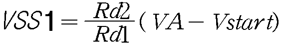
전압 시프트(420`)는 복수의 저항(Rd1-Rd5) 및 증폭기(421`)를 포함한다. 증폭기(421`)은 신호(E/D)에 의해 제어된다. 구체적으로, 신호(E/D)가 로우 레벨에서 하이 레벨로 변경되는 시점에 동기되어 동작을 시작하고, 하이 레벨에서 로우 레벨로 변경되는 시점에 동기되어 그 시점의 소프트 스타트 전압(VSS1)을 유지한다. 증폭기(421`)는 제1 전압(VCC)이 두 개의 저항(Rd5) 및 저항(Rd6)의 저항비에 의해 분배된 전압(VA)과 스타트 전압(Vstart)의 차를 증폭하여 소프트 스타트 전압(VSS1)을 생성한다. 이를 나타내면 수학식 1과 같다. 이렇게 생성된 소프트 스타트 전압(VSS)는 PWM 제어부(440`)에 전달된다. 증폭기(421`)는 신호(E/D)에 의해 동작을 멈추면, 그 시점의 소프트 스타트 전압(VSS1)을 유지한다.The
피드백 신호 생성부(430`)는 두 개의 다이오드(D5, D6), 두 개의 저항(R1, R2), 전류원(Idelay`) 및 전류원(Ifb`)을 포함한다. 다이오드(D5)의 캐소드 전극은 커패시터(Cfb)(도 1 참조)의 일단에 연결되어, 다이오드(D5)의 캐소드 전극에는 피 드백 전압(Vfb)이 인가된다. 그리고 전류원(Idelay`)의 전류는 커패시터(Cfb)로 흐른다. 다이오드(D5)의 애노드 전극 및 다이오드(D6)의 애노드 전극은 서로 연결되어 있으며, 전류원(Ifb`)의 전류는 다이오드(D5) 및 다이오드(D6)를 통해 양쪽으로 나뉘어 흐른다. 저항(R1)의 일단은 다이오드(D6)의 캐소드 전극에 연결되어 있고, 저항(R1)의 타단은 저항(R2)의 일단 및 PWM 제어부(440`)의 비교기(441`)의 두 개의 비반전 단자(+) 중 하나에 연결되어 있다. 저항(R2)의 타단은 접지되어 있다. 전류원(Ifb`)의 전류 중 다이오드(D6)를 통해 흐르는 전류가 저항(R1) 및 저항(R2)을 흐르며 발생하는 전압이 피드백 신호(VF`)의 전압이 된다. 이렇게 생성된 전압(VF`)는 피드백 전압(Vfb)이 저항(R1) 및 저항(R2)의 저항비에 의해 분배된 전압과 같다. The
PWM 제어부(440`)는 PWM 비교기(441`), 인버터(442`), OSC(443`), 제3 플립플롭(444`), NOR 게이트(445`) 및 게이트 드라이버(446`)를 포함한다.The PWM controller 440 'includes a
PWM 비교기(441`)는 소프트 스타트 전압(VSS), 피드백 신호(VF`) 및 감지 전압(Vsense)을 입력받고, 소프트 스타트 전압(VSS1) 및 피드백 신호(VF`) 중 낮은 전압 레벨을 가지는 것과 감지 전압(Vsense)을 비교한다. PWM 비교기(441`)은 비교 결과에 따라 신호(U5)를 생성한다. 구체적으로, 소프트 스타트 전압(VSS1)이 피드백 신호(VF`)보다 낮은 기간에서, PWM 비교기(441`)는 소프트 스타트 전압(VSS)과 감지 전압(Vsense)을 비교한 결과에 따라 신호(U5)를 생성한다. 반대로, 피드백 신호(VF`)가 소프트 스타트 전압(VSS1)보다 낮은 기간에서, PWM 비교기(441`)는 피드백 신호(VF`)와 감지 전압(Vsense)을 비교한 결과에 따라 신호(U5)를 생성한다. 예를 들면, 피드백 신호(VF`)가 소프트 스타트 전압(VSS1)보다 낮은 기간동안, 신호(U5)는 피드백 신호(VF`)가 감지 전압(Vsense) 이상이면, 하이 레벨이 되고, 피드백 신호(VF`)가 감지 전압(Vsense)보다 작으면, 로우 레벨이 된다. The
인버터(442`)는 입력된 신호(U5)를 반전시켜 신호(U6)을 생성하고, 제3 플립플롭(444`)의 리셋단(R)으로 전달한다.The
오실레이터(443`)는 소정의 주기를 가지는 클록 신호(CLK)를 생성하여 제3 플립플롭(444`)의 셋단(S) 및 NOR 게이트(445`)로 전달한다.The
제3 플립플롭(444`)은 신호(U6) 및 클록 신호(CLK)에 따라 신호(U7)를 생성하여 NOR 게이트(445`)로 전달한다. 본 발명의 제2 실시 예에 따른 제3 플립플롭(444`)은 본 발명의 제1 실시 예에 따른 제2 플립플롭(453)과 동일한 방식으로 동작한다. 제3 플립플롭(444`)는 셋단(S) 및 리셋단(R)에 입력되는 신호에 따라 신호(U7)을 생성하여 출력단(/Q)를 통해 NOR 게이트(445`)로 전달한다.The third flip-
NOR 게이트(445`)는 클록 신호(CLK) 및 신호(U7)를 NOR 연산하여, 신호(U8)를 생성하고 게이트 드라이버(446`)로 전달한다. The NOR
게이트 드라이버(446`)는 하이 레벨의 신호(U8)에 따라 스위치(M)을 도통시킬 수 있는 전압 레벨을 가지는 게이트 제어 신호(Vg)를 생성하여 스위치(M)의 게이트 전극으로 출력한다. 그리고 로우 레벨의 신호(U8)에 따라 스위치(M)를 차단시킬 수 있는 전압 레벨을 가지는 게이트 제어 신호(Vg)를 생성하여 스위치(M)의게이트 전극으로 출력한다. The
이하, 본 발명의 제2 실시 예에 따른 스위치 제어 방법 및 컨버터 구동 방법 에 대해서 도 10을 참조하여 설명한다.Hereinafter, a switch control method and a converter driving method according to the second embodiment of the present invention will be described with reference to FIG. 10.
도 10은 본 발명의 제2 실시 예에 따른 스위치 제어 장치(400`)의 제1 전압(VCC), 피드백 신호(VF`), 감지 전압(Vsense), 소프트 스타트 전압(VSS1), 및 컨버터의 출력 전압(Vout)을 나타낸 파형도이다.FIG. 10 is a diagram illustrating a first voltage VCC, a feedback signal VF`, a sense voltage Vsense, a soft start voltage VSS1, and a converter of a
제1 전압(VCC)이 제1 레벨의 기준 전압(VR)이 되는 시점(T21)에 소프트 스타트가 시작된다. 소프트 스타트가 시작되면, 소프트 스타트 전압(VSS1)이 증가하기 시작한다. 소프트 스타트 전압(VSS1)은 출력 전압(Vout)이 정상화 되는 시점(T22)까지는 피드백 신호(VF`)의 전압보다 낮은 레벨을 갖는다. 따라서 기간(T21-T22)동안, PWM 제어부(440`)의 비교기(441`)는 감지 전압(Vsense)과 소프트 스타트 전압(VSS1)을 비교하여, 비교 결과에 따른 신호(U5)를 생성한다. 감지 전압(Vsense)이 소프트 스타트 전압(VSS)과 같아지면, 신호(U5)는 로우 레벨이 되고, 인버터(442`)에 의해 생성된 신호(U6)는 하이 레벨이 된다. 제3 플립플롭(444`)의 리셋단(R)에 하이 레벨의 신호(U6)가 전달되면, 출력단(/Q)을 통해 하이 레벨의 신호(U7)가 NOR 게이트(445`)로 전달된다. 그러면, NOR 게이트(445`)는 로우 레벨의 신호(U8)를 생성하여, 게이트 드라이버(446`)로 신호(U8)를 전달한다. 게이트 드라이버(446`)는 신호(U8)에 따라 스위치(M)을 차단시키는 게이트 제어 신호(Vg)를 스위치(M)의 게이트 전극으로 전달한다. 스위치(M)가 차단되면, 스위치(M)에 전류는 흐르지 않으므로, 감지 전압(Vsense)은 발생하지 않는다. 감지 전압(Vsense)이 소프트 스타트 전압(VSS1)보다 낮아지므로, 비교기(441`)으로부터 출력되는 신호(U5)는 하이 레벨이 되고, 제3 플립플롭(444`)의 리셋단(R)에 입력되는 신호(U6)는 로 우 레벨이 된다. 그 이후 클록 신호가 하이 레벨로 변경되는 시점에 제3 플립플롭(444`)은 로우 레벨의 신호(U7)을 출력한다. 그러면, NOR 게이트(445`)는 하이 레벨의 신호(U8)을 게이트 드라이버(446`)로 전달한다. 게이트 드라이버(456`)는 하이 레벨의 신호(U8)에 따라 스위치(M)를도통시키는 게이트 제어 신호(Vg)를 스위치(M)의 게이트 전극에 전달한다. 스위치(M)은 도통되고, 스위치(M)를흐르는 전류는 다시 상승하여, 감지 전압(Vsense)은 증가한다. 이와 같은 방식으로, 감지 전압(Vsense)이 발생하고, 감지 전압(Vsense)의 피크치는 기간(T21-T22)동안 소프트 스타트 전압(VSS1)에 의해 제어된다. The soft start is started at a time point T21 when the first voltage VCC becomes the reference voltage VR of the first level. When the soft start is started, the soft start voltage VSS1 starts to increase. The soft start voltage VSS1 has a level lower than the voltage of the feedback signal VF ′ until the time point T22 at which the output voltage Vout is normalized. Therefore, during the periods T21-T22, the
시점(T22)에 출력 전압(Vout)이 정상화 되면, 피드백 전압(Vfb)은 급격히 감소하고, 피드백 신호(VF`)도 그에 따라 감소한다. 피드백 신호(VF`)는 시점(T22)이후, 소프트 스타트 전압(VSS1)보다 작아지며, 이 시점부터 감지 전압(Vsense)의 피크치는 피드백 신호(VF`)에 의해 제어된다. 즉, 피드백 전압(Vfb)에 따라 스위치(M)에 흐르는 전류의 피크값이 결정된다. 그리고 시점(T23)에 제1 전압(VCC)이 제2 레벨의 기준 전압(VR)과 동일해지면, 소프트 스타트 설정 기간이 종료한다.When the output voltage Vout is normalized at the time point T22, the feedback voltage Vfb decreases rapidly, and the feedback signal VF 'also decreases accordingly. The feedback signal VF` becomes smaller than the soft start voltage VSS1 after the time point T22. From this point in time, the peak value of the sense voltage Vsense is controlled by the feedback signal VF`. That is, the peak value of the current flowing through the switch M is determined according to the feedback voltage Vfb. When the first voltage VCC becomes equal to the reference voltage VR of the second level at the time point T23, the soft start setting period ends.
또한, 본 발명의 제2 실시 예에 따른 스위치 제어 장치(400`)는 본 발명의 제1 실시 예에 따른 스위치 제어 장치(400)가 포함하는 음기울기 검출부(450)를 포함할 수 있다.In addition, the
도 11은 본 발명의 제3 실시 예에 따른 스위치 제어 장치(400``)로서 음기울기 검출부(450`)를 포함하는 스위치 제어 장치(400``)를 나타낸 도면이다.FIG. 11 is a view illustrating a
도 11에 도시된 바와 같이, 음기울기 검출부(450`)는 피드백 전압을 입력받 고, 소프트 스타트 종료 신호(SE1)를 전압 시프터(420``)로 전달한다.As illustrated in FIG. 11, the slope
전압 시프터(420``)는 소프트 스타트 종료 신호(SE1)에 응답하여 소프트 스타트 전압(VSS2)을 설정된 최대값으로 생성하여 출력한다. 이 때, 최대값은 피드백 신호(VF`)가 가질 수 있는 가장 높은 전압 레벨보다 높은 레벨이다. 그러면, PWM 제어부(440`)는 소프트 스타트가 종료된 시점으로부터, 소프트 스타트 전압(VSS2)보다 낮은 전압 신호인 피드백 신호(VF`)와 감지 전압(Vsense)을 이용하여 스위치(M)의 차단 시점을 결정한다. 이하, 다른 구성 및 그 연결관계는 본 발명의 제2 실시 예에 따른 스위칭 제어장치(400`)와 동일하다.The
도 12는 본 발명의 제3 실시 예에 따른 스위치 제어 장치(400``)의 구성을 구체적으로 나타낸 도면이다.12 is a view showing in detail the configuration of the
도 12에 도시된 바와 같이, 음기울기 검출부(450`)의 소프트 스타트 종료 신호(SE1)가 전압 시프터(420``)로 전달된다. 구체적으로, 전압 시프터(420``)의 증폭기(421``)는 소프트 스타트 종료 신호(SE1)가 전달되면, 소프트 스타트 종료 신호(SE1)가 전달된 시점에 동기되어 설정된 소프트 스타트 전압(VSS2)의 최대값을 생성하여 PWM 제어부(440`)의 비교기(441`)의 비반전단자(+)로 출력한다. 그러면 비교기(451`)은 감지 전압(Vsense)과 피드백 신호(VF`)의 전압을 비교하여 신호(U5)를 생성한다. 이하, 나머지 구성, 그 연결관계 및 동작은 동일하다. As illustrated in FIG. 12, the soft start end signal SE1 of the
본 발명의 제2 실시예 및 제3 실시 예에 따른 소프트 스타트 전압(VSS1) 및 소프트 스타트 전압(VSS2)의 차이에 대해서 도 13을 참조하여 설명한다.Differences between the soft start voltage VSS1 and the soft start voltage VSS2 according to the second and third embodiments of the present invention will be described with reference to FIG. 13.
도 13은 본 발명의 제3 실시 예에 따른 스위치 제어 장치(400``)의 제1 전 압(VCC), 피드백 신호(VF`), 감지 전압(Vsense), 제2 실시 예에 따른 소프트 스타트 전압(VSS1), 제3 실시 예에 따른 소프트 스타트 전압(VSS2) 및 컨버터의 출력 전압(Vout)을 나타낸 파형도이다. FIG. 13 illustrates a first voltage VCC, a feedback signal VF`, a sense voltage Vsense, and a soft start according to a second embodiment of the
도 13에 도시된 바와 같이, 시점 T22에 출력 전압이 정상화 되어 피드백 전압(Vfb)이 감소하면, 피드백 신호(VF`)도 감소한다. 이 때, 본 발명의 제3 실시 예에 따른 소프트 스타트 전압(VSS2)은 제2 실시 예의 소프트 스타트 전압(VSS1)과 달리 소프트 스타트 종료 신호(SE1)에 의해 설정된 최대 소프트 스타트 전압까지 증가한다.As shown in FIG. 13, when the output voltage is normalized at the time point T22 and the feedback voltage Vfb decreases, the feedback signal VF ′ also decreases. In this case, unlike the soft start voltage VSS1 of the second embodiment, the soft start voltage VSS2 increases to the maximum soft start voltage set by the soft start end signal SE1.
이하, 본 발명의 제 4 실시 예에 따른 스위칭 제어장치 및 이를 포함하는 컨버터에 대해서 설명한다.Hereinafter, a switching control apparatus and a converter including the same according to a fourth embodiment of the present invention will be described.
도 14는 본 발명의 제4 실시 예에 따른 컨버터를 간단히 나타낸 도면이다.14 is a diagram schematically illustrating a converter according to a fourth embodiment of the present invention.
본 발명의 제4 실시 예에 따른 컨버터는 스위치(Qsw), 스위치 제어 장치(800), 피드백 신호 생성부(900), 커패시터(C11), 다이오드(D11) 및 인덕터(L11)를 포함한다. 본 발명의 제4 실시 예에 따른 스위치(Qsw)는 MOSFET(metal oxcide semiconductor field effect transistor) 소자로서, 게이트 전극, 소스 전극 및 드레인 전극을 포함하고, n-채널 타입이다.The converter according to the fourth embodiment of the present invention includes a switch Qsw, a
커패시터(C11)의 양단은 출력단에 연결되어 출력 전압(Vout)의 리플 성분을 필터링한다. 인덕터(L11)는 커패시터(C11)의 일단 및 출력단의 (+)단에 연결되어 있다. 다이오드(D11)은 인덕터(L11)의 타단에 캐소드 전극이 연결되고, 애노드 전극은 출력단의 (-)단에 연결되어 있다. 커패시터(C11) 및 인덕터(L11)은 LC 필터를 형성하여 입력 전압의 교류 성분을 제거하고, 출력 전압(Vout)을 생성한다. 다이오드(D11)는 프리휠링 경로(Freewheeling Path)를 형성하기 위한 것으로, 스위치(Qsw)가 차단되더라도 커패시터(C11) 및 다이오드(D11)를 경유하는 경로를 통해 인덕터(L11)에 축적된 전류를 흘려주기 위한 것이다. Both ends of the capacitor C11 are connected to the output terminal to filter the ripple component of the output voltage Vout. The inductor L11 is connected to one end of the capacitor C11 and the positive end of the output terminal. The cathode of the diode D11 is connected to the other end of the inductor L11, and the anode of the diode D11 is connected to the negative end of the output terminal. Capacitor C11 and inductor L11 form an LC filter to remove the alternating current component of the input voltage and generate an output voltage Vout. The diode D11 is for forming a freewheeling path. Even though the switch Qsw is blocked, the diode D11 flows the current accumulated in the inductor L11 through the path through the capacitor C11 and the diode D11. It is to give.
피드백 신호 생성부(900)는 인덕터(L11)의 양단에 인가되는 전압을 이용하여, 피드백 신호를 생성하여 스위치 제어 장치(800)로 전달하는 역할을 수행한다. 피드백 신호 생성부(900)는 스위치(Qsw)가 턴오프되어 있는 동안, 인덕터(L11)의 양단에는 출력 전압(Vout)과 같은 크기의 전압이 인가되며, 피드백 신호 생성부(900)는 이를 샘플 및 홀딩(sample and holding)한 뒤 소정의 전압 범위로 전압 분배하여, 피드백 신호(VFB)를 생성한다. 피드백 신호 생성부(900)는 피드백 신호(VFB)를 스위치 제어 장치(800)의 음기울기 검출부(820) 및 PWM 제어부(830)에 전달한다.The
스위치 제어 장치(800)는 소프트 스타트 전압 생성부(810), 음기울기 검출부(820) 및 PWM 제어부(830)를 포함한다.The
소프트 스타트 전압 생성부(810)는 입력 전압(Vin)을 이용하여 제1 전압(VCC)을 생성한다. 이 때, 제1 전압(VCC)을 생성하는 구성은 본 발명의 제1 내지 제3 실시 예에 설명한 것과 동일하다. 이렇게 생성된 제1 전압(VCC)을 이용하여 본 발명의 제4 실시 예에 따른 소프트 스타트 전압 생성부(810)는 본 발명의 제1 내지 제3 실시 예에 기재한 방식에 따라 소프트 스타트 전압(VSS3)을 생성한다. 또한, 소프트 스타트 전압 생성부(810)가 소프트 스타트 전압(VSS3)을 생성하는 방식 역 시 본 발명의 제1 내지 제3 실시 예에서 설명한 구성과 동일한다. 구체적으로, 본 발명의 제1 실시 예에 따르면, 전류원 배열부(도 4의 420)에서 생성되는 전류(Ifb)가 소정의 저항값을 가지는 저항에 흐를 때 발생하는 전압 신호를 소프트 스타트 전압(VSS3)으로 생성할 수 있다. 또한, 본 발명의 제2 및 제3 실시 예에 따른 소프트 스타트 전압(VSS1, VSS2)을 생성하는 방식을 그대로 사용할 수 있다. 소프트 스타트 전압 생성부(810)는 이렇게 생성한 소프트 스타트 전압(VSS3)을 PWM 제어부(830)로 전달한다. The soft
음기울기 검출부(820)는 본 발명의 제1 및 제3 실시 예에서 설명한 것과 동일하게 피드백 신호(VFB)를 전달받고, 피드백 신호(VFB)가 감소하는 시점을 검출한다. 음기울기 검출부(820)는 그 시점에 소프트 스타트 종료 신호(SE2)를 생성하여, 소프트 스타트 전압 생성부(810)로 전달한다. 그러면, 소프트 스타트 전압 생성부(810)는 소프트 스타트 종료 신호(SE3)에 따라 피드백 신호(VFB)의 최대 레벨보다 높은 레벨로 소프트 스타트 전압(VSS3)을 증가시킨 후, 이 레벨로 소프트 스타트 전압(VSS3)을 유지한다.The
PWM 제어부(830)는 소프트 스타트 전압(VSS3) 및 피드백 신호(VFB)의 전압 중 낮은 레벨의 전압과 소정 레벨의 기준 전압을 비교하여, 스위칭 동작을 제어한다. 초기 동작시 소프트 스타트 전압(VSS3)은 피드백 신호(VFB)보다 낮은 레벨이고, PWM 제어부(830)는 기준 전압이 소프트 스타트 전압(VSS3)에 도달하면, 스위치(Qsw)를 차단시킨다. 소프트 스타트 전압 생성부(810)는 소프트 스타트 종료 신호(SE2)를 전달받으면, 피드백 신호(VFB)의 최대 레벨보다 높은 레벨로 소프트 스 타트 전압(VSS3)을 유지한다. 따라서, PWM 제어부(830)는 소프트 스타트 전압(VSS3)보다 낮은 피드백 전압(VFB)을 이용하여 스위칭 동작을 제어한다. PWM 제어부(830)는 기준 전압이 피드백 신호(VFB)에 도달하면, 스위치(Qsw)를 차단시킨다. PWM 제어부(830)는 내부적으로 소정의 주기를 가지는 클록 신호를 생성하는 오실레이터(도시하지 않음)를 포함하여, 이렇게 차단된 시점 이후, 클록 신호의 라이징 에지등의 시점에 동기되어 차단된 스위치(Qsw)를 도통 시킬 수 있다.The
이와 같이 본 발명의 실시 예에 따른 스위치 제어 장치는 컨버터에 적용되어 소프트 스타트를 제어하는데 사용될 수 있다. 그러면, 종래 카운터, 디지털/아날로그 변환기와 같은 크기가 크고 복잡한 구조를 가지는 회로 없이 소프트 스타트 방식을 구현할 수 있다. As such, the switch control device according to the embodiment of the present invention may be applied to a converter and used to control a soft start. Then, the soft start method can be implemented without a circuit having a large and complicated structure such as a conventional counter and a digital-to-analog converter.
또한, 본 발명의 제1 내지 제4 실시 예에서 설명한 스위치 및 스위치 제어 장치는 하나의 칩(IC)으로 구성될 수 있다. 또한, 스위치 및 스위치 제어 장치 각각이 별개의 패키지로 되어 있고, 이를 이용하여 하나의 칩으로 구성할 수 있다. In addition, the switch and the switch control device described in the first to fourth embodiments of the present invention may be configured as one chip (IC). In addition, each switch and the switch control device is a separate package, it can be configured as a single chip.
상기 도면과 발명의 상세한 설명은 단지 본 발명의 예시적인 것으로서, 이는 단지 본 발명을 설명하기 위한 목적에서 사용된 것이지 의미 한정이나 특허청구범위에 기재된 본 발명의 범위를 제한하기 위하여 사용된 것은 아니다. 그러므로 본 기술 분야의 통상의 지식을 가진 자라면 이로부터 다양한 변형 및 균등한 타 실시예가 가능하다는 점을 이해할 것이다. 따라서, 본 발명의 진정한 기술적 보호 범위는 첨부된 특허청구범위의 기술적 사상에 의해 정해져야 할 것이다. The drawings and the detailed description of the invention are merely illustrative of the invention and are used merely for the purpose of describing the invention and not for limiting the scope of the invention as set forth in the claims or the claims. Therefore, those skilled in the art will appreciate that various modifications and equivalent embodiments are possible without departing from the scope of the present invention. Accordingly, the true scope of the present invention should be determined by the technical idea of the appended claims.
이상에서와 같이 본 발명에 의하면, 간단한 구조를 갖고, 정확한 소프트 스타트 제어가 가능한 스위치 제어 장치 및 제어 방법, 이를 이용하는 컨버터 및 그 구동방법을 제공한다.As described above, the present invention provides a switch control device and control method having a simple structure and capable of accurate soft start control, a converter using the same, and a driving method thereof.
또한, 소프트 스타트 설정 기간 동안에도, 온도 증가에 따른 스위치에 흐르는 전류의 피크 값이 감소하는 것을 방지할 수 있는 스위치 제어 장치 및 제어 방법, 이를 이용하는 컨버터 및 그 구동방법을 제공한다.In addition, during the soft start setting period, the present invention provides a switch control device and control method capable of preventing the peak value of the current flowing through the switch from decreasing with increasing temperature, a converter using the same, and a driving method thereof.
Claims (53)
Priority Applications (3)
| Application Number | Priority Date | Filing Date | Title |
|---|---|---|---|
| KR1020070040242A KR101370650B1 (en) | 2007-04-25 | 2007-04-25 | Switch contoller, a control method of the switch, the converter, and the driving method using the switch contoller and the control method of the switch |
| US12/150,226 US8169802B2 (en) | 2007-04-25 | 2008-04-25 | Switch controller of a converter with a soft start signal generator comprising a plurality of current sources |
| US13/438,777 US8670252B2 (en) | 2007-04-25 | 2012-04-03 | Switch controller, switch control method, converter using the same, and driving method thereof |
Applications Claiming Priority (1)
| Application Number | Priority Date | Filing Date | Title |
|---|---|---|---|
| KR1020070040242A KR101370650B1 (en) | 2007-04-25 | 2007-04-25 | Switch contoller, a control method of the switch, the converter, and the driving method using the switch contoller and the control method of the switch |
Publications (2)
| Publication Number | Publication Date |
|---|---|
| KR20080095567A KR20080095567A (en) | 2008-10-29 |
| KR101370650B1 true KR101370650B1 (en) | 2014-03-10 |
Family
ID=39886758
Family Applications (1)
| Application Number | Title | Priority Date | Filing Date |
|---|---|---|---|
| KR1020070040242A Active KR101370650B1 (en) | 2007-04-25 | 2007-04-25 | Switch contoller, a control method of the switch, the converter, and the driving method using the switch contoller and the control method of the switch |
Country Status (2)
| Country | Link |
|---|---|
| US (2) | US8169802B2 (en) |
| KR (1) | KR101370650B1 (en) |
Cited By (1)
| Publication number | Priority date | Publication date | Assignee | Title |
|---|---|---|---|---|
| KR102121202B1 (en) * | 2019-01-03 | 2020-06-10 | 주식회사 유니솔렉 | High voltage supply available for controlling output according to detecting abnormal state, and method for detecting abnormal state using thereof |
Families Citing this family (38)
| Publication number | Priority date | Publication date | Assignee | Title |
|---|---|---|---|---|
| US8742740B2 (en) * | 2008-09-19 | 2014-06-03 | Power Integrations, Inc. | Digital peak input voltage detector for a power converter controller |
| US8416587B2 (en) * | 2008-11-20 | 2013-04-09 | Silergy Technology | Synchronous rectifier control circuits and methods of controlling synchronous rectifiers |
| KR101042220B1 (en) * | 2009-05-15 | 2011-06-20 | 고려대학교 산학협력단 | Soft-Start Circuits and DC-DC Converters and Their Driving Methods |
| TWI436187B (en) * | 2009-07-21 | 2014-05-01 | Richtek Technology Corp | Feedback circuit and control method of an isolated power converter |
| US9225251B2 (en) | 2009-07-29 | 2015-12-29 | Delta Electronics, Inc. | Duty cycle control method, power supply system and power converter using the same |
| CN101989814B (en) * | 2009-07-29 | 2013-10-09 | 台达电子工业股份有限公司 | Voltage Regulating Circuit and Its Applicable Parallel Voltage Regulating Circuit System |
| CN102177646A (en) * | 2009-12-30 | 2011-09-07 | 世派电子株式会社 | switch mode power supply |
| KR101677729B1 (en) * | 2010-02-19 | 2016-11-18 | 페어차일드코리아반도체 주식회사 | Switch control device, power supply device comprising the same, and switch control method |
| US8476878B2 (en) * | 2010-11-15 | 2013-07-02 | National Semiconductor Corporation | Startup circuit for DC-DC converter |
| JP2012161117A (en) * | 2011-01-28 | 2012-08-23 | Rohm Co Ltd | Dc/dc converter, and power supply device and electronic apparatus using the same |
| TWI440288B (en) * | 2011-03-11 | 2014-06-01 | Neoenergy Microelectronics Inc | Start control circuit with accelerated start function and operation method thereof |
| JP2013005631A (en) * | 2011-06-17 | 2013-01-07 | Sony Corp | Switching power supply apparatus |
| TWI454036B (en) * | 2012-01-09 | 2014-09-21 | Richtek Technology Corp | Bridge rectifier for a pfc power converter |
| TWI463780B (en) * | 2012-11-16 | 2014-12-01 | Noveltek Semiconductor Corp | Isolated power converter, inverting type shunt regulator, and operating method thereof |
| US9921627B2 (en) | 2013-01-08 | 2018-03-20 | Semiconductor Components Industries, Llc | Control circuit for programmable power supply |
| US9203383B2 (en) * | 2013-03-14 | 2015-12-01 | Sandisk Technologies Inc. | Digital soft start with continuous ramp-up |
| US9774257B2 (en) * | 2014-05-23 | 2017-09-26 | Allegro Microsystems, Llc | Control circuit for a switching regulator driving an LED load with controlled PWM dimming |
| TWI551022B (en) * | 2014-11-11 | 2016-09-21 | Dynamic drive capability adjustment of the power control device | |
| US9831777B2 (en) * | 2015-06-29 | 2017-11-28 | Fairchild Korea Semicondcutor Ltd. | Switch control circuit and converter including the same |
| US9812976B2 (en) * | 2015-06-30 | 2017-11-07 | Fairchild Semiconductor Corporation | Control of a startup circuit using a feedback pin of a PWM controller integrated circuit chip |
| KR102444416B1 (en) | 2015-11-25 | 2022-09-16 | 한국전기연구원 | Soft-Switching Method of Motors Providing Kickstart |
| CN106253887A (en) * | 2016-07-28 | 2016-12-21 | 苏州律力电子科技有限公司 | A kind of soft start switch Circuits System |
| US9806617B1 (en) * | 2016-09-09 | 2017-10-31 | Dialog Semiconductor (Uk) Limited | Switch mode power converter with overshoot and undershoot transient control circuits |
| CN107846141B (en) * | 2016-10-12 | 2020-04-14 | 昆山启达微电子有限公司 | Power supply starting circuit |
| US10250252B2 (en) | 2016-11-03 | 2019-04-02 | Semiconductor Components Industries, Llc | Control circuit and method therefor |
| US10784784B2 (en) * | 2017-05-23 | 2020-09-22 | Semiconductor Components Industries, Llc | DC-DC converter with dynamic feedback loop |
| US10320301B2 (en) | 2017-09-15 | 2019-06-11 | Semiconductor Components Industries, Llc | Power converter responsive to device connection status |
| WO2019165461A1 (en) * | 2018-02-26 | 2019-08-29 | Chaoyang Semiconductor Jiangyin Technology Co., Ltd. | Method and apparatus for improving integrity of processor voltage supply with overshoot mitigation and support for dvfs |
| JP2020124010A (en) * | 2019-01-29 | 2020-08-13 | キヤノン株式会社 | Control device, exposure apparatus, and item production method |
| US10914627B2 (en) * | 2019-02-13 | 2021-02-09 | Semtech Corporation | Configurable laser monitor photodiode in optical modulation amplitude controller |
| KR102679564B1 (en) * | 2019-11-01 | 2024-06-27 | 삼성전자주식회사 | Transmitter circuit, method of data transmission and electronic system |
| TWI748518B (en) * | 2020-06-15 | 2021-12-01 | 瑞昱半導體股份有限公司 | Optical receiver device, pulse width modulation controller circuitry, and sensitivity control method |
| CN113824319B (en) * | 2020-06-19 | 2025-03-04 | 瑞昱半导体股份有限公司 | Optical receiver device, pulse width modulator circuit system and sensitivity control method |
| CN111799761A (en) * | 2020-06-24 | 2020-10-20 | 华源智信半导体(深圳)有限公司 | Temperature protection method and circuit based on pin multiplexing |
| TWI726808B (en) * | 2020-09-04 | 2021-05-01 | 新唐科技股份有限公司 | Under voltage lock out circuit and operating method thereof |
| US11736016B2 (en) | 2021-08-25 | 2023-08-22 | Dialog Semiconductor (Uk) Limited | Switching converter with improved load transient response and method of operating the same |
| KR102376309B1 (en) * | 2021-12-20 | 2022-03-17 | 이수훈 | Power supply |
| US12456971B2 (en) | 2023-11-30 | 2025-10-28 | Allegro Microsystems, Llc | Method and apparatus for limiting minority carrier injection |
Citations (4)
| Publication number | Priority date | Publication date | Assignee | Title |
|---|---|---|---|---|
| US5430635A (en) | 1993-12-06 | 1995-07-04 | Bertonee, Inc. | High power factor electronic transformer system for gaseous discharge tubes |
| US5805434A (en) | 1995-01-17 | 1998-09-08 | Vlt Corporation | Control of stored magnetic energy in power converter transformers |
| KR100603420B1 (en) * | 1999-06-03 | 2006-07-20 | 페어차일드코리아반도체 주식회사 | Switching-mode power supplies |
| KR100625768B1 (en) | 1998-12-09 | 2006-12-05 | 페어차일드코리아반도체 주식회사 | Feedback Circuit in Switched-Mode Power Supplies |
Family Cites Families (6)
| Publication number | Priority date | Publication date | Assignee | Title |
|---|---|---|---|---|
| US6344980B1 (en) * | 1999-01-14 | 2002-02-05 | Fairchild Semiconductor Corporation | Universal pulse width modulating power converter |
| US6633193B1 (en) | 2002-04-08 | 2003-10-14 | Wells Fargo Bank Minnesota, National Association, As Collateral Agent | Method of forming a switching device and structure therefor |
| US7088078B2 (en) * | 2004-06-04 | 2006-08-08 | Astec International Limited | Soft-start circuit for power converters |
| CN100490287C (en) * | 2004-12-03 | 2009-05-20 | 罗姆股份有限公司 | Switching power supply, control circuit therefor, and electronic device using same |
| JP4823604B2 (en) * | 2005-08-05 | 2011-11-24 | ローム株式会社 | Soft start circuit, power supply, electrical equipment |
| US7928715B2 (en) * | 2008-04-22 | 2011-04-19 | Seiko Instruments Inc. | Switching regulator |
-
2007
- 2007-04-25 KR KR1020070040242A patent/KR101370650B1/en active Active
-
2008
- 2008-04-25 US US12/150,226 patent/US8169802B2/en active Active
-
2012
- 2012-04-03 US US13/438,777 patent/US8670252B2/en active Active
Patent Citations (4)
| Publication number | Priority date | Publication date | Assignee | Title |
|---|---|---|---|---|
| US5430635A (en) | 1993-12-06 | 1995-07-04 | Bertonee, Inc. | High power factor electronic transformer system for gaseous discharge tubes |
| US5805434A (en) | 1995-01-17 | 1998-09-08 | Vlt Corporation | Control of stored magnetic energy in power converter transformers |
| KR100625768B1 (en) | 1998-12-09 | 2006-12-05 | 페어차일드코리아반도체 주식회사 | Feedback Circuit in Switched-Mode Power Supplies |
| KR100603420B1 (en) * | 1999-06-03 | 2006-07-20 | 페어차일드코리아반도체 주식회사 | Switching-mode power supplies |
Cited By (1)
| Publication number | Priority date | Publication date | Assignee | Title |
|---|---|---|---|---|
| KR102121202B1 (en) * | 2019-01-03 | 2020-06-10 | 주식회사 유니솔렉 | High voltage supply available for controlling output according to detecting abnormal state, and method for detecting abnormal state using thereof |
Also Published As
| Publication number | Publication date |
|---|---|
| US8670252B2 (en) | 2014-03-11 |
| US8169802B2 (en) | 2012-05-01 |
| US20080266907A1 (en) | 2008-10-30 |
| KR20080095567A (en) | 2008-10-29 |
| US20120188802A1 (en) | 2012-07-26 |
Similar Documents
| Publication | Publication Date | Title |
|---|---|---|
| KR101370650B1 (en) | Switch contoller, a control method of the switch, the converter, and the driving method using the switch contoller and the control method of the switch | |
| CN110994998B (en) | Switching power supply device and control method thereof | |
| US6980444B2 (en) | Switching power supply | |
| JP5115317B2 (en) | Switching power supply | |
| US8310845B2 (en) | Power supply circuit with a control terminal for different functional modes of operation | |
| KR101677729B1 (en) | Switch control device, power supply device comprising the same, and switch control method | |
| US8295062B2 (en) | Switching power supply apparatus and semiconductor device | |
| KR101739550B1 (en) | Thermal shutdown unit, switch controller comprising the same, and control method of thermal shut down protection operation | |
| JP6745585B2 (en) | Switching power supply | |
| KR101527966B1 (en) | Switch mode power supply and its driving method | |
| US10170906B2 (en) | Semiconductor device for power supply control | |
| EP3264580A1 (en) | Semiconductor device for controlling power source | |
| CN111641340B (en) | Switching power supply device | |
| JP6860118B2 (en) | Power factor improvement circuit and semiconductor device | |
| JP2009284667A (en) | Power supply device, its control method, and semiconductor device | |
| KR20170118729A (en) | Semiconductor device for power control | |
| US7558084B2 (en) | Switching mode power supply with compensated propagation delay | |
| JP7602389B2 (en) | Power supply control device and flyback converter | |
| JP2005198375A (en) | Synchronous rectifier circuit and power converter | |
| US9112353B2 (en) | Power supply device | |
| US10622901B2 (en) | Low loss IC self supply | |
| KR101284827B1 (en) | A switch contoller, a control method of the switch, and a converter using the switch controller | |
| US20250105746A1 (en) | Switching power supply device and power control semiconductor device | |
| JP2024099139A (en) | Switching Power Supply Unit |
Legal Events
| Date | Code | Title | Description |
|---|---|---|---|
| PA0109 | Patent application |
Patent event code: PA01091R01D Comment text: Patent Application Patent event date: 20070425 |
|
| PG1501 | Laying open of application | ||
| A201 | Request for examination | ||
| PA0201 | Request for examination |
Patent event code: PA02012R01D Patent event date: 20120418 Comment text: Request for Examination of Application Patent event code: PA02011R01I Patent event date: 20070425 Comment text: Patent Application |
|
| E902 | Notification of reason for refusal | ||
| PE0902 | Notice of grounds for rejection |
Comment text: Notification of reason for refusal Patent event date: 20130514 Patent event code: PE09021S01D |
|
| E701 | Decision to grant or registration of patent right | ||
| PE0701 | Decision of registration |
Patent event code: PE07011S01D Comment text: Decision to Grant Registration Patent event date: 20131226 |
|
| GRNT | Written decision to grant | ||
| PR0701 | Registration of establishment |
Comment text: Registration of Establishment Patent event date: 20140227 Patent event code: PR07011E01D |
|
| PR1002 | Payment of registration fee |
Payment date: 20140227 End annual number: 3 Start annual number: 1 |
|
| PG1601 | Publication of registration | ||
| FPAY | Annual fee payment |
Payment date: 20170117 Year of fee payment: 4 |
|
| PR1001 | Payment of annual fee |
Payment date: 20170117 Start annual number: 4 End annual number: 4 |
|
| FPAY | Annual fee payment |
Payment date: 20180212 Year of fee payment: 5 |
|
| PR1001 | Payment of annual fee |
Payment date: 20180212 Start annual number: 5 End annual number: 5 |
|
| FPAY | Annual fee payment |
Payment date: 20190207 Year of fee payment: 6 |
|
| PR1001 | Payment of annual fee |
Payment date: 20190207 Start annual number: 6 End annual number: 6 |
|
| PR1001 | Payment of annual fee |
Payment date: 20210202 Start annual number: 8 End annual number: 8 |
|
| PR1001 | Payment of annual fee |
Payment date: 20220125 Start annual number: 9 End annual number: 9 |
|
| PR1001 | Payment of annual fee |
Payment date: 20230126 Start annual number: 10 End annual number: 10 |
|
| PR1001 | Payment of annual fee |
Payment date: 20240130 Start annual number: 11 End annual number: 11 |
|
| PR1001 | Payment of annual fee |
Payment date: 20250210 Start annual number: 12 End annual number: 12 |