KR101273760B1 - Transparent electode, transparent antena and method for manufacturing the transparent electode - Google Patents
Transparent electode, transparent antena and method for manufacturing the transparent electode Download PDFInfo
- Publication number
- KR101273760B1 KR101273760B1 KR1020110002413A KR20110002413A KR101273760B1 KR 101273760 B1 KR101273760 B1 KR 101273760B1 KR 1020110002413 A KR1020110002413 A KR 1020110002413A KR 20110002413 A KR20110002413 A KR 20110002413A KR 101273760 B1 KR101273760 B1 KR 101273760B1
- Authority
- KR
- South Korea
- Prior art keywords
- metal
- transparent conductive
- layer
- conductive oxide
- transparent
- Prior art date
- Legal status (The legal status is an assumption and is not a legal conclusion. Google has not performed a legal analysis and makes no representation as to the accuracy of the status listed.)
- Expired - Fee Related
Links
Images


Classifications
-
- H—ELECTRICITY
- H01—ELECTRIC ELEMENTS
- H01B—CABLES; CONDUCTORS; INSULATORS; SELECTION OF MATERIALS FOR THEIR CONDUCTIVE, INSULATING OR DIELECTRIC PROPERTIES
- H01B5/00—Non-insulated conductors or conductive bodies characterised by their form
- H01B5/14—Non-insulated conductors or conductive bodies characterised by their form comprising conductive layers or films on insulating-supports
-
- H—ELECTRICITY
- H01—ELECTRIC ELEMENTS
- H01B—CABLES; CONDUCTORS; INSULATORS; SELECTION OF MATERIALS FOR THEIR CONDUCTIVE, INSULATING OR DIELECTRIC PROPERTIES
- H01B1/00—Conductors or conductive bodies characterised by the conductive materials; Selection of materials as conductors
- H01B1/02—Conductors or conductive bodies characterised by the conductive materials; Selection of materials as conductors mainly consisting of metals or alloys
-
- H—ELECTRICITY
- H01—ELECTRIC ELEMENTS
- H01B—CABLES; CONDUCTORS; INSULATORS; SELECTION OF MATERIALS FOR THEIR CONDUCTIVE, INSULATING OR DIELECTRIC PROPERTIES
- H01B1/00—Conductors or conductive bodies characterised by the conductive materials; Selection of materials as conductors
- H01B1/06—Conductors or conductive bodies characterised by the conductive materials; Selection of materials as conductors mainly consisting of other non-metallic substances
- H01B1/08—Conductors or conductive bodies characterised by the conductive materials; Selection of materials as conductors mainly consisting of other non-metallic substances oxides
-
- H—ELECTRICITY
- H01—ELECTRIC ELEMENTS
- H01B—CABLES; CONDUCTORS; INSULATORS; SELECTION OF MATERIALS FOR THEIR CONDUCTIVE, INSULATING OR DIELECTRIC PROPERTIES
- H01B13/00—Apparatus or processes specially adapted for manufacturing conductors or cables
- H01B13/0026—Apparatus for manufacturing conducting or semi-conducting layers, e.g. deposition of metal
Landscapes
- Engineering & Computer Science (AREA)
- Manufacturing & Machinery (AREA)
- Manufacturing Of Electric Cables (AREA)
- Laminated Bodies (AREA)
Abstract
본 발명은 저저항 다층 구조의 다층 투명 전도막과 금속선을 혼합한 새로운 형태의 투명전극 및 그 제조방법을 제공하는 것이다. 본 발명에 의한 투명전극은, 다층 투명 전도막과 다층 투명 전도막의 일면에 접하는 복수의 금속선을 포함한다. 다층 투명 전도막은 투명 전도성 산화물층 및 투명 전도성 산화물층과 접하는 금속층을 포함하고, 금속층의 상하면에 투명 전도성 산화물층이 적층된 2n+1층(n은 1 이상의 정수)의 샌드위치 구조를 갖는다. 본 발명에 의한 투명전극은 저저항 다층 구조의 다층 투명 전도막과 금속선이 혼합된 새로운 형태의 투명전극으로 우수한 투과성과 전도성을 가지므로, 평판 디스플레이, 터치 패널, 태양전지, 센서, TFT 등 다양한 전자소자에 이용될 수 있다.The present invention provides a novel transparent electrode and a method of manufacturing the same, in which a multilayer transparent conductive film having a low resistance multilayer structure and a metal wire are mixed. The transparent electrode according to the present invention includes a multilayer transparent conductive film and a plurality of metal wires in contact with one surface of the multilayer transparent conductive film. The multilayer transparent conductive film includes a transparent conductive oxide layer and a metal layer in contact with the transparent conductive oxide layer, and has a sandwich structure of 2n + 1 layers (n is an integer of 1 or more) in which a transparent conductive oxide layer is stacked on the upper and lower surfaces of the metal layer. The transparent electrode according to the present invention is a new type of transparent electrode in which a multi-layer transparent conductive film having a low resistance multilayer structure and a metal wire are mixed and have excellent permeability and conductivity, so that various electronics such as flat panel display, touch panel, solar cell, sensor, TFT, etc. It can be used for the device.
Description
본 발명은 투명전극에 관한 것으로, 더욱 상세하게는 높은 전도도와 가시광 영역에서의 높은 투과도를 갖는 투명전극과 이를 이용한 투명 안테나 및 투명전극의 제조방법에 관한 것이다.The present invention relates to a transparent electrode, and more particularly to a transparent electrode having a high conductivity and high transmittance in the visible light region, and a transparent antenna and a method for manufacturing the transparent electrode using the same.
최근 휴대폰은 무선 인터넷 통신망의 발달과 더불어 단순히 통화만을 위한 장비에서 벗어나 GPS, DMB, Wi-Fi등 기존 컴퓨터가 가진 대부분의 역할을 수행하고 있다. 이러한 무선 통신의 수신을 위해서는 각 영역대 별로 많은 안테나가 필요하게 된다.Recently, with the development of wireless Internet communication network, mobile phone is playing the role of existing computer such as GPS, DMB, Wi-Fi, etc. In order to receive such wireless communication, many antennas are required for each area band.
그러나 휴대성을 위해 제한된 크기로 제작되어야만 하는 휴대폰의 특성상 안테나의 설치 공간은 제약적일 수밖에 없다. 휴대폰용 안테나로 주로 사용되고 있는 금속 안테나는 매우 낮은 저항으로 우수한 특성을 보이며 활용되고 있지만, 불투명하므로 휴대폰의 내부에 많은 공간을 차지하며 설치된다.However, due to the characteristics of a mobile phone that must be manufactured in a limited size for portability, the installation space of the antenna is limited. Metal antennas, which are mainly used as antennas for mobile phones, are being used with excellent characteristics with very low resistance, but because they are opaque, they are installed taking up a lot of space inside the mobile phones.
이러한 문제점을 해결하기 위해 최근 플렉시블 투명전극을 안테나로 활용하는 방법이 제안되고 있다. 플렉시블 투명전극이란 PET, PES, PEN과 같은 플렉시블 기판 상에 상막시킨 높은 전도도와 가시광선 영역에서의 높은 투과도를 가지는 전극 물질을 의미하는 것으로, 유연성을 갖기 때문에 플렉시블 전자기기의 전극으로 응용이 가능하다. 플렉시블 투명전극은 플렉시블 소자용 전극뿐만 아니라, 면저항 크기에 따라 정전기 방지막, 안테나, 광학 필터로도 응용이 가능한 것으로 알려져 있다. 플렉시블 투명전극은 투명하므로 휴대폰의 표면이나 내부 등 공간의 제약 없이 설치가 가능하다.In order to solve this problem, a method of using a flexible transparent electrode as an antenna has recently been proposed. The flexible transparent electrode refers to an electrode material having high conductivity and high transmittance in the visible light region formed on a flexible substrate such as PET, PES, and PEN. Since it is flexible, it can be applied as an electrode of a flexible electronic device. . The flexible transparent electrode is known to be applicable not only to an electrode for a flexible element but also to an antistatic film, an antenna, and an optical filter according to the sheet resistance. Since the flexible transparent electrode is transparent, it can be installed without limitation of space such as the surface or the inside of the mobile phone.
플렉시블 투명전극으로는 주로 투명 전도성 산화물(ITO, IZO 등)이 이용된다. 현재 휴대폰용 안테나로 제작되는 금속 안테나의 경의 1~3 × 10⁻⁶Ω·cm의 비저항 값을 가지므로, 플렉시블 투명전극 역시 이에 준하는 비저항 값을 가져야 원활한 수신율을 기대할 수 있다.As the flexible transparent electrode, transparent conductive oxides (ITO, IZO, etc.) are mainly used. Since a metal antenna manufactured as an antenna for a mobile phone has a specific resistance value of 1 to 3 × 10 -6 Ω · cm, the flexible transparent electrode must also have a specific resistivity corresponding to the smooth reception rate.
그런데 플렉시블 투명전극의 제조에 이용되는 투명 전도성 산화물은 전도도를 나타내는 비저항 값이 10-4Ω·cm이하 값을 가질 수 없다. 따라서, 현재 알려진 투명 전도성 산화물로 투명 안테나를 제작할 경우, 기존 금속 안테나와 같은 수신율을 기대하기 어렵다.However, the transparent conductive oxide used in the manufacture of the flexible transparent electrode may not have a specific resistance value of 10 −4 Ω · cm or less. Therefore, when manufacturing a transparent antenna with a transparent conductive oxide currently known, it is difficult to expect the same reception rate as a conventional metal antenna.
본 발명은 이러한 점을 감안하여 안출된 것으로, 본 발명의 목적은 저저항 다층 구조의 다층 투명 전도막과 금속선을 혼합한 새로운 형태의 투명전극 및 그 제조방법을 제공하는 것이다.SUMMARY OF THE INVENTION The present invention has been made in view of this point, and an object of the present invention is to provide a novel transparent electrode and a manufacturing method of a multi-layer transparent conductive film having a low resistance multilayer structure and a metal wire.
본 발명의 다른 목적은 다층 투명 전도막과 금속선을 혼합한 새로운 형태의 평판형 투명전극을 이용함으로써, 원활한 수신율을 갖고 설치에 있어서의 공간적 제약을 크게 줄일 수 있는 투명 안테나를 제공하는 것을 목적으로 한다.Another object of the present invention is to provide a transparent antenna having a smooth reception rate and greatly reducing spatial constraints in installation by using a new type of flat transparent electrode in which a multilayer transparent conductive film and a metal wire are mixed. .
상기 목적을 달성하기 위한 본 발명에 의한 투명전극은, 다층 투명 전도막과 상기 다층 투명 전도막의 일면에 접하는 복수의 금속선을 포함한다. 상기 다층 투명 전도막은 투명 전도성 산화물층 및 상기 투명 전도성 산화물층과 접하는 금속층을 포함하고, 상기 금속층의 상하면에 상기 투명 전도성 산화물층이 적층된 2n+1층(n은 1 이상의 정수)의 샌드위치 구조를 갖는다.The transparent electrode according to the present invention for achieving the above object includes a multilayer transparent conductive film and a plurality of metal wires in contact with one surface of the multilayer transparent conductive film. The multilayer transparent conductive film includes a transparent conductive oxide layer and a metal layer in contact with the transparent conductive oxide layer, and has a sandwich structure of a 2n + 1 layer (n is an integer of 1 or more) in which the transparent conductive oxide layer is stacked on upper and lower surfaces of the metal layer. Have
상기 다층 투명 전도막은 그 두께가 일정하고, 상기 복수의 금속선을 부분적으로 감쌀 수 있도록 상기 복수의 금속선에 대응하는 부분이 상기 금속선의 두께에 대응하는 높이로 융기될 수 있다.The multilayer transparent conductive film may have a constant thickness, and a portion corresponding to the plurality of metal wires may be raised to a height corresponding to the thickness of the metal wire so as to partially wrap the plurality of metal wires.
상기 금속층과 상기 금속선은 동일한 금속 물질로 이루어질 수 있다.The metal layer and the metal wire may be made of the same metal material.
상기 금속 물질은 Ag, Au, Cu, Al. Pt, Pd, Cr, Ti, W, Nb, Ta, V, Ca, Fe, Mn, Co, Ni, Zn 중에서 선택될 수 있다.The metal material is Ag, Au, Cu, Al. It may be selected from Pt, Pd, Cr, Ti, W, Nb, Ta, V, Ca, Fe, Mn, Co, Ni, Zn.
상기 복수의 금속선은 일정한 형태의 메시를 형성하는 그물망 구조로 배치될 수 있다.The plurality of metal wires may be arranged in a mesh structure forming a mesh of a predetermined shape.
상기 복수의 금속선 중 일부는 제 1 방향으로 배치되고, 나머지 일부는 상기 제 1 방향과 직교하는 제 2 방향으로 배치될 수 있다.Some of the plurality of metal wires may be disposed in a first direction, and some of the metal wires may be disposed in a second direction perpendicular to the first direction.
상기 목적을 달성하기 위한 본 발명에 의한 투명 안테나는, 투명 기판, 상기 투명 기판 위에 놓이는 복수의 금속선, 상기 투명 기판 위에 적층되어 상기 복수의 금속선을 덮는 다층 투명 전도막을 포함한다. 상기 다층 투명 전도막은 투명 전도성 산화물층 및 상기 투명 전도성 산화물층과 접하는 금속층을 포함하되, 상기 금속층의 상하면에 상기 투명 전도성 산화물층이 적층된 2n+1층(n은 1 이상의 정수)의 샌드위치 구조를 갖는다.A transparent antenna according to the present invention for achieving the above object includes a transparent substrate, a plurality of metal wires placed on the transparent substrate, a multilayer transparent conductive film stacked on the transparent substrate to cover the plurality of metal wires. The multilayer transparent conductive film may include a transparent conductive oxide layer and a metal layer in contact with the transparent conductive oxide layer, wherein a sandwich structure of a 2n + 1 layer (n is an integer of 1 or more) in which the transparent conductive oxide layer is stacked on upper and lower surfaces of the metal layer is formed. Have
상기 목적을 달성하기 위한 본 발명에 의한 투명전극의 제조방법은, 기판 위에 복수의 금속선을 형성하는 단계, 상기 복수의 금속선이 형성된 상기 기판 위에 상기 복수의 금속선을 덮도록 다층 투명 전도막을 형성하는 단계를 포함한다. 상기 다층 투명 전도막을 형성하는 단계는, 상기 복수의 금속선이 형성된 상기 기판 위에 상기 복수의 금속선을 덮도록 투명 전도성 산화물층을 형성하는 단계, 상기 투명 전도성 산화물층 위에 금속층을 형성하는 단계, 상기 금속층 위에 투명 전도성 산화물층을 형성하는 단계를 포함하되, 상기 금속층의 상하면에 상기 투명 전도성 산화물층이 배치되어 전체적으로 2n+1층(n은 1 이상의 정수)의 샌드위치 구조가 되도록 상기 투명 전도성 산화물층 및 상기 금속층을 적층한다.In the method of manufacturing a transparent electrode according to the present invention for achieving the above object, forming a plurality of metal lines on a substrate, forming a multi-layer transparent conductive film to cover the plurality of metal lines on the substrate on which the plurality of metal lines are formed It includes. The forming of the multilayer transparent conductive film may include forming a transparent conductive oxide layer on the substrate on which the plurality of metal lines are formed to cover the plurality of metal lines, forming a metal layer on the transparent conductive oxide layer, and on the metal layer. Forming a transparent conductive oxide layer, wherein the transparent conductive oxide layer is disposed on the upper and lower surfaces of the metal layer so that the transparent conductive oxide layer and the metal layer have a sandwich structure of 2n + 1 layers (n is an integer of 1 or more). Laminated.
상기 금속선을 형성하는 단계는, 상기 복수의 금속선의 배치 구조에 대응하는 패턴홈을 갖는 패턴 마스크를 상기 기판 위에 배치하는 단계, 상기 금속층과 같은 재질의 금속 타겟을 이용한 스퍼터 공정을 통해 상기 금속 타겟의 입자를 상기 패턴홈을 통과시켜 상기 기판 위에 입사시키는 단계를 포함할 수 있다.The forming of the metal line may include disposing a pattern mask having a pattern groove corresponding to an arrangement structure of the plurality of metal lines on the substrate, and sputtering the metal target by using a metal target made of the same material as the metal layer. Passing the particles through the pattern groove may be incident on the substrate.
상기 금속선을 형성하는 단계는, 상기 기판 위에 포토레지스트층을 형성하는 단계, 상기 복수의 금속선의 배치 구조에 대응하는 패턴을 갖는 포토 마스크를 상기 포토레지스트층 위에 배치하고 상기 포토 마스크의 패턴에 따라 상기 포토레지스트층을 노광하는 단계, 상기 포토레지스트층을 현상하여 상기 포토레지스트층에 상기 복수의 금속선의 배치 구조에 대응하는 패턴홈을 형성하는 단계, 상기 패턴홈에 상기 금속선을 구성하기 위한 금속 물질을 도포하는 단계, 상기 포토레지스트층을 제거하는 단계를 포함할 수 있다.The forming of the metal line may include forming a photoresist layer on the substrate, and disposing a photomask having a pattern corresponding to the arrangement structure of the plurality of metal lines on the photoresist layer and in accordance with the pattern of the photomask. Exposing a photoresist layer, developing the photoresist layer to form a pattern groove corresponding to an arrangement structure of the plurality of metal lines in the photoresist layer, and forming a metal material for forming the metal line in the pattern groove. It may include the step of applying, removing the photoresist layer.
상기 투명 전도막을 형성하는 각각의 단계는, 상기 투명 전도성 산화물층과 동일한 재질의 산화물 타겟과 상기 금속층과 동일한 재질의 금속 타겟을 이용한 스퍼터 공정을 통해 차례로 수행될 수 있다.Each step of forming the transparent conductive film may be sequentially performed through a sputtering process using an oxide target of the same material as the transparent conductive oxide layer and a metal target of the same material as the metal layer.
상기 스퍼터 공정은, 상기 복수의 금속선이 형성된 상기 기판, 상기 산화물 타겟이 구비된 제 1 스퍼터건, 상기 금속 타겟이 구비된 제 2 스퍼터건을 같은 진공 챔버에 넣고, 상기 제 1 스퍼터건 및 상기 제 2 스퍼터건을 교대로 작동시켜 상기 기판 위에 상기 투명 전도성 산화물층 및 상기 금속층을 차례로 적층할 수 있다.The sputtering step includes placing the substrate on which the plurality of metal lines are formed, the first sputter gun provided with the oxide target, and the second sputter gun provided with the metal target in the same vacuum chamber, and the first sputter gun and the first agent. The two sputter guns may be operated alternately to sequentially stack the transparent conductive oxide layer and the metal layer on the substrate.
본 발명에 의한 투명전극의 제조방법은, 상기 기판으로 필름형의 플렉시블 기판을 이용하고, 상기 플렉시블 기판의 이동 경로 중에 상기 금속선과 동일한 재질의 금속 타겟을 갖는 제 1 스퍼터건과 상기 투명 전도 산화물층과 동일한 재질의 산화물 타겟을 갖는 제 2 스퍼터건과 상기 금속층과 동일한 재질의 금속 타겟을 갖는 제 3 스퍼터건과 상기 전도 산화물 타겟을 갖는 제 4 스퍼터건을 차례로 배치하되, 상기 플렉시블 기판과 상기 제 1 스퍼터건 사이에는 상기 복수의 금속선의 배치 구조에 대응하는 패턴홈을 갖는 패턴 마스크를 배치하고, 상기 플렉시블 기판을 이동시키면서 상기 제 1 스퍼터건, 상기 제 2 스퍼터건, 상기 제 3 스퍼터건 및 상기 제 4 스퍼터건을 작동시켜 상기 플렉시블 기판 위에 상기 복수의 금속선, 상기 투명 전도 산화물층, 상기 금속층 및 상기 투명 전도 산화물층을 형성할 수 있다.In the method for manufacturing a transparent electrode according to the present invention, a first sputter gun and a transparent conductive oxide layer using a film-type flexible substrate as the substrate, and having a metal target having the same material as that of the metal wire in a moving path of the flexible substrate. A second sputter gun having an oxide target of the same material and a third sputter gun having a metal target of the same material as the metal layer and a fourth sputter gun having the conductive oxide target are disposed in this order, wherein the flexible substrate and the first A pattern mask having a pattern groove corresponding to the arrangement structure of the plurality of metal wires is disposed between the sputter guns, and the first sputter gun, the second sputter gun, the third sputter gun, and the first sputter gun are moved while the flexible substrate is moved. 4 sputter guns to operate the plurality of metal wires, the transparent conductive oxide layer, And a metal layer can be formed in the transparent conductive oxide layer.
본 발명에 의한 투명전극은 저저항 다층 구조의 다층 투명 전도막과 금속선이 혼합된 새로운 형태의 투명전극으로 우수한 투과성과 전도성을 가지므로, 평판 디스플레이, 터치 패널, 태양전지, 센서, TFT 등 다양한 전자소자에 이용될 수 있다.The transparent electrode according to the present invention is a new type of transparent electrode in which a multi-layer transparent conductive film having a low resistance multilayer structure and a metal wire are mixed and have excellent permeability and conductivity, so that various electronics such as flat panel display, touch panel, solar cell, sensor, TFT, etc. It can be used for the device.
또한, 본 발명에 의한 투명전극은 휴대폰용 안테나, 차량용 안테나, GPS 수신용 안테나, DMB 수신 안테나, 블루투스 수신용 안테나, Wi-Fi 수신용 안테나 등 전파 수신이 필요한 다양한 장치의 안테나로 이용될 수 있다. 이러한 투명 안테나는 우수한 투명성을 가지고 있어서, 건물용 유리, 차량용 유리, 휴대폰의 윈도우창 등에 삽입 설치될 수 있으며, 설치에 필요한 공간을 줄여 주고, 제품의 미적 효과 및 디자인 자유도를 높여줄 수 있다.In addition, the transparent electrode according to the present invention can be used as an antenna of various devices that require radio wave reception, such as antenna for a mobile phone, a vehicle antenna, a GPS receiving antenna, a DMB receiving antenna, a Bluetooth receiving antenna, a Wi-Fi receiving antenna. . Since the transparent antenna has excellent transparency, it can be inserted into a building glass, a vehicle glass, a window of a mobile phone, etc., and can reduce the space required for installation, and enhance the aesthetic effect and design freedom of the product.
도 1은 투명 기판 위에 형성된 본 발명의 일실시예에 의한 투명전극을 나타낸 것이다.
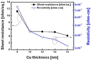
도 2는 NTO-Ag-NTO 구조의 다층 박막에 있어서 Ag층의 두께에 따른 면저항 및 비저항 측정 결과를 나타낸 것이다.
도 3은 NTO-Ag-NTO 구조의 다층 박막에 있어서 Ag층의 두께에 따른 투과율 측정 결과를 나타낸 것이다.
도 4는 NTO-Cu-NTO 구조의 다층 박막에 있어서 Cu층의 두께에 따른 면저항 및 비저항 측정 결과를 나타낸 것이다.
도 5는 NTO-Cu-NTO 구조의 다층 박막에 있어서 Cu층의 두께에 따른 투과율 측정 결과를 나타낸 것이다.
도 6은 본 발명에 의한 투명전극을 제조하기 위한 롤투롤 스퍼터링 장치를 나타낸 것이다.
도 7은 포토리소그래피 공정과 박막 형성 공정을 이용하여 본 발명에 의한 투명전극을 제조하는 과정을 나타낸 것이다.
도 8은 본 발명에 의한 투명전극을 제조하기 위한 스퍼터 장치를 나타낸 것이다.
도 9는 포토리소그래피 공정 및 스퍼터 공정을 이용하여 제조한 본 발명의 시험예에 의한 투명전극의 면저항 측정 결과를 나타낸 것이다.
도 10은 포토리소그래피 공정 및 스퍼터 공정을 이용하여 제조한 본 발명의 시험예에 의한 투명전극의 투과율 측정 결과를 나타낸 것이다.
도 11은 상술한 시험예를 통해 제조한 투명전극을 이용한 안테나의 효율을 기존의 구리 안테나와 비교하여 나타낸 것이다.1 shows a transparent electrode according to an embodiment of the present invention formed on a transparent substrate.
Figure 2 shows the sheet resistance and resistivity measurement results according to the thickness of the Ag layer in the multi-layer thin film of the NTO-Ag-NTO structure.
Figure 3 shows the transmittance measurement results according to the thickness of the Ag layer in the multi-layer thin film of the NTO-Ag-NTO structure.
Figure 4 shows the sheet resistance and specific resistance measurement results according to the thickness of the Cu layer in the NTO-Cu-NTO multilayer thin film.
Figure 5 shows the transmittance measurement results according to the thickness of the Cu layer in the multilayer thin film of the NTO-Cu-NTO structure.
Figure 6 shows a roll-to-roll sputtering apparatus for manufacturing a transparent electrode according to the present invention.
7 shows a process of manufacturing a transparent electrode according to the present invention using a photolithography process and a thin film formation process.
8 shows a sputtering apparatus for manufacturing a transparent electrode according to the present invention.
9 shows the sheet resistance measurement results of the transparent electrode according to the test example of the present invention manufactured using the photolithography process and the sputtering process.
10 shows the results of measuring the transmittance of the transparent electrode according to the test example of the present invention manufactured using the photolithography process and the sputtering process.
Figure 11 shows the efficiency of the antenna using a transparent electrode prepared by the above-described test example compared with the conventional copper antenna.
이하에서는 첨부된 도면을 참조하여, 본 발명의 일실시예에 의한 투명전극과 이를 이용한 투명 안테나 및 투명전극의 제조방법에 대하여 상세히 설명한다.Hereinafter, with reference to the accompanying drawings, a transparent electrode according to an embodiment of the present invention and a method of manufacturing a transparent antenna and a transparent electrode using the same will be described in detail.
본 발명을 설명함에 있어서, 도면에 도시된 구성요소의 크기나 형상 등은 설명의 명료성과 편의를 위해 과장되거나 단순화되어 나타날 수 있다. 또한, 본 발명의 구성 및 작용을 고려하여 특별히 정의된 용어들은 사용자, 운용자의 의도 또는 관례에 따라 달라질 수 있다. 이러한 용어들은 본 명세서 전반에 걸친 내용을 토대로 본 발명의 기술적 사상에 부합하는 의미와 개념으로 해석되어야 한다.In describing the present invention, the sizes and shapes of the components shown in the drawings may be exaggerated or simplified for clarity and convenience of explanation. In addition, terms defined in consideration of the configuration and operation of the present invention may be changed according to the intention or custom of the user, the operator. These terms are to be construed in accordance with the meaning and concept consistent with the technical idea of the present invention based on the contents throughout the present specification.
도 1은 투명 기판 위에 형성된 본 발명의 일실시예에 의한 투명전극을 나타낸 것이다.1 shows a transparent electrode according to an embodiment of the present invention formed on a transparent substrate.
도 1에 도시된 것과 같이, 본 발명의 일실시예에 의한 투명전극(10)은 한 쌍의 투명 전도 산화물층(12)(14)과 금속층(13)을 갖는 다층 투명 전도막(11)과 다층 투명 전도막(11)의 일면에 배치되는 복수의 금속선(16)을 포함한다. 다층 투명 전도막(11)은 제 1 투명 전도 산화물층(12)과 제 2 투명 전도 산화물층(14) 사이에 금속층(13)이 개재된 샌드위치 구조로 이루어진다.As shown in FIG. 1, the
제 1 투명 전도 산화물층(12) 및 제 2 투명 전도 산화물층(14)은 투명 전도성 산화물(Transparent Conducting Oxide: TCO)로 이루어진다. 투명 전도성 산화물은 가시광선 영역에서의 높은 광학적 투과도(85% 이상)와 낮은 비저항(1×10⁻³ Ω·cm)을 동시에 갖는 산화물계의 축퇴된(degenerate) 반도체 전극이다. 이러한 투명 전도성 산화물로는 ITO, ZnO, SnO2, TiO2 등이 있다. 금속층(13)은 Ag, Au, Cu, Al. Pt, Pd, Cr, Ti, W, Nb, Ta, V, Ca, Fe, Mn, Co, Ni, Zn 등의 금속 물질로 이루어진다.The first transparent
본 발명에 의한 투명전극(10)의 다층 투명 전도막(11)과 같은 산화물층-금속층-산화물층 구조의 다층 박막은 최근 고품질 플렉시블 투명전극에 대한 필요성이 대두되면서 투명전극으로 연구되고 있다. 박형 산화물층 사이에 개재된 Ag로 대표되는 금속층은 특정 두께에서 그 상하부의 산화물층과 antireflection 효과를 일으켜 광투과도를 높여준다. 예컨대, 10 ~ 15nm 두께의 Ag층이 삽입된 다층 박막은 단층 박막보다 높은 광투과도를 나타낸다. 또한, 이러한 다층 박막은 비저항이 낮은 금속층을 삽입하였기 때문에 금속층의 두께를 적절히 조절하면 광투과성과 상온에서도 금속에 버금가는 면저항과 비저항을 가진 투명전극으로 이용될 수 있다.The multilayer thin film of the oxide layer-metal layer-oxide layer structure, such as the multilayer transparent
본 출원인은 ITO-Ag-ITO, ITO-Cu-ITO, AZO-Ag-AZO, GZO-Ag-GZO, IZO-Ag-IZO, IZTO-Ag-IZTO, NTO-Ag-NTO, NTO-Cu-NTO 등 다양한 다층 박막을 제작하고, 이들 다층 박막의 투명전극으로의 적용 가능성을 확인한 바 있다.Applicants are ITO-Ag-ITO, ITO-Cu-ITO, AZO-Ag-AZO, GZO-Ag-GZO, IZO-Ag-IZO, IZTO-Ag-IZTO, NTO-Ag-NTO, NTO-Cu-NTO Various multilayer thin films were produced, and the applicability of these multilayer thin films to transparent electrodes was confirmed.
일 예로, 도 2 및 도 3은 NTO-Ag-NTO 구조의 다층 박막에 있어 Ag층의 두께에 따른 면저항(sheet resistance) 및 비저항(resistivity) 측정 결과, 투과율(transmittance) 측정 결과를 나타낸 것이다. 여기에서, NTO층은 6wt%의 Nb2O5가 도핑된 TiO2 타겟을 이용한 스퍼터 공정을 통해 유리 기판 위에 30nm 두께로 형성한 것이고, Ag층 역시 스퍼터 공정을 통해 NTO층 위에 형성한 것이다. 또한, 도 4 및 도 5는 Ag 대신 Cu를 이용한 NTO-Cu-NTO 구조의 다층 박막에 있어 Cu층의 두께에 따른 면저항 및 비저항 측정 결과, 투과율 측정 결과를 나타낸 것이다.For example, FIGS. 2 and 3 show the results of measuring sheet resistance and resistivity according to the thickness of the Ag layer, and measuring the transmittance of the multilayer thin film of the NTO-Ag-NTO structure. Here, the NTO layer is formed to a thickness of 30nm on the glass substrate through a sputtering process using a TiO 2 target doped with 6wt% Nb 2 O 5 , Ag layer is also formed on the NTO layer through a sputtering process. 4 and 5 show the results of measuring the sheet resistance and the resistivity according to the thickness of the Cu layer and the transmittance measurement results in the multilayer thin film of the NTO-Cu-NTO structure using Cu instead of Ag.
이들 결과를 살펴보면, 금속층의 두께를 적절히 조절하면 다양한 광전소자에 적용할 수 있을 정도의 면저항, 비저항 및 투과도를 갖는 산화물층-금속층-산화물층 구조의 다층 박막을 구현할 수 있음을 알 수 있다.Looking at these results, it can be seen that if the thickness of the metal layer is properly adjusted, it is possible to implement a multilayer thin film having an oxide layer-metal layer-oxide layer structure having sheet resistance, specific resistance, and transmittance enough to be applied to various optoelectronic devices.
다시 도 1을 참조하면, 다층 투명 전도막(11)은 그 두께가 전체적으로 일정하며, 복수의 금속선(16)을 부분적으로 감쌀 수 있도록 복수의 금속선(16)에 대응하는 부분이 융기되어 있다. 다층 투명 전도막(11)의 융기부(15)는 금속선(16)에 대응하는 형상과 금속선(16)의 두께에 대응하는 높이로 융기된 것이다. 다층 투면 전도막(11)은 투명 기판(2) 위에 금속선(16)이 형성된 후, 그 위에 적층되는 것이므로, 융기부(15)는 별도의 성형 공정없이 형성 다층 투명 전도막(11)의 형성시 자연스럽게 형성된다.Referring to FIG. 1 again, the multilayer transparent
금속선(16)은 Ag, Au, Cu, Al. Pt, Pd, Cr, Ti, W, Nb, Ta, V, Ca, Fe, Mn, Co, Ni, Zn 등의 금속 물질로 이루어진다. 금속선(16)은 공정 상의 편의를 위해 금속층(13)과 같은 물질로 이루어지는 것이 좋다. 복수의 금속선(16)은 정사각형의 메시(17)를 형성하는 그물망 구조로 배치된다. 이를 위해 복수의 금속선(16) 중 일부는 제 1 방향으로 일정한 간격으로 배치되고, 나머지 일부는 제 1 방향과 직교하는 제 2 방향으로 일정한 간격으로 배치된다. 본 발명에 의한 투명전극(10)은 금속선(16)의 높은 전도도로 인해 우수한 전도성을 갖게 된다.
앞에서는 본 발명에 의한 투명전극(10)의 다층 투명 전도막(11)이 제 1 투명 전도 산화물층-금속층-제 2 투명 전도 산화물층의 3층 구조를 갖는 것으로 설명하였으나, 다층 투명 전도막(11)의 구조가 이러한 3층 구조로 한정되는 것은 아니다. 즉, 다층 투명 전도막(11)은 한 쌍 이상의 투명 전도 산화물층(12)(14)과 하나 이상의 금속층(13)을 포함하되, 금속층(13)의 상하면에 투명 전도 산화물층(12)(14)이 각각 적층된 2n+1층(n은 1 이상의 정수)의 다양한 멀티 스택 구조를 가질 수 있다.In the above, the multilayer transparent
또한, 복수의 금속선(16)의 배치 구조는 도 1에 도시된 것과 같은 격자 배치 구조로 한정되지 않고, 다양하게 변경될 수 있다. 예컨대, 복수의 금속선(16)은 삼각형, 직사각형, 마름모, 벌집 모양 등 다양한 형태의 메시를 형성하도록 그물망 구조로 배치될 수 있다. 다른 예로, 복수의 금속선(16)은 서로 교차하지 않도록 배치될 수도 있다.In addition, the arrangement structure of the plurality of
이러한 본 발명에 의한 투명전극(10)은 저저항 다층 구조의 다층 투명 전도막(11)과 금속선(16)이 혼합되어 우수한 투과성과 전도성을 가지므로, 평판 디스플레이, 터치 패널, 태양전지, 센서, TFT 등 다양한 전자소자의 제조에 이용될 수 있다.Since the
또한, 본 발명에 의한 투명전극(10)은 투명 기판(2)과 함께 투명 안테나를 구성할 수 있다. 이러한 투명 안테나는 휴대폰용 안테나, 차량용 안테나, GPS 수신용 안테나, DMB 수신 안테나, 블루투스 수신용 안테나, Wi-Fi 수신용 안테나 등 전파 수신이 필요한 다양한 장치의 안테나로 이용될 수 있다. 투명 안테나는 건물용 유리, 차량용 유리, 휴대폰의 윈도우창 등에 삽입 설치될 수 있어서, 안테나 설치에 따른 공간을 줄여주고, 제품의 미적 효과 및 디자인 자유도를 높여줄 수 있다.본 발명에 의한 투명전극은 롤투롤 스퍼터(roll-to-roll sputter) 공정, 스퍼터(sputter) 공정, 증착(evaporation) 공정 등 다양한 성막 공정을 통해 제조될 수 있다.In addition, the
도 6은 롤투롤 스퍼터 공정을 위한 롤투롤 스퍼터링 장치를 나타낸 것이다.6 shows a roll-to-roll sputtering apparatus for a roll-to-roll sputter process.
롤투롤 스퍼터 공정을 이용하기 위해 기판으로는 필름형의 플렉시블 기판(4)을 이용한다. 롤투롤 스퍼터 장치는 진공 챔버(20)와 플렉시블 기판(4)의 이동 경로 중에 차례로 배치되는 복수의 스퍼터건(21)(22)(23)(24)을 구비한다. 제 1 스퍼터건(21)은 금속선(16)을 형성하기 위한 것으로 금속선(16)과 동일한 재질의 금속 타겟(25)을 갖고, 제 2 스퍼터건(22)은 제 1 투명 전도 산화물층(12)을 형성하기 위한 것으로 제 1 투명 전도 산화물층(12)과 동일한 재질의 산화물 타겟(26)을 갖는다. 제 3 스퍼터건(23)은 금속층(13)을 형성하기 위한 것으로 금속층(13)과 동일한 재질의 금속 타겟(27)을 갖고, 제 4 스퍼터건(24)은 제 2 투명 전도 산화물층(14)을 형성하기 위한 것으로 제 2 투명 전도 산화물층(14)과 동일한 재질의 산화물 타겟(28)을 갖는다. 플렉시블 기판(4)과 제 1 스퍼터건(21) 사이에는 설정된 금속선(16)의 배치 구조에 대응하는 패턴홈(31)을 갖는 패턴 마스크(30)가 배치된다.In order to use the roll-to-roll sputtering process, a film-shaped
도 1과 도 6을 참조하면 먼저, 진공 챔버(20)를 공정 압력으로 만들고 공정 가스를 진공 챔버(20)에 주입하면서 리와인더(33)와 와인더(34)를 이용하여 플렉시블 기판(4)을 냉각드럼(35) 둘레를 따라 이동시킨다. 플렉시블 기판(4)이 이동하면 제 1 스퍼터건(21)을 작동시켜 금속 타겟(25)에 플라즈마를 유도하여 금속 타겟(25)의 입자를 패턴 마스크(30)의 패턴홈(31)을 통과시켜 플렉시블 기판(4) 위에 입사시킨다. 이때, 플렉시블 기판(4) 위에 패턴홈(31) 모양대로 금속선(16)이 형성된다.Referring to FIGS. 1 and 6, first, the
금속선(16)의 형성 후, 제 2 스퍼터건(22)을 작동시켜 산화물 타겟(26)에 플라즈마를 유도하여 전도 산화물 입자를 금속선(16)이 형성된 플렉시블 기판(4) 위에 증착시켜 제 1 투명 전도 산화물층(12)을 형성한다. 다음으로, 제 3 스퍼터건(23)을 작동시켜 금속 타겟(27)에 플라즈마를 유도하여 제 1 투명 전도 산화물층(12) 위에 금속층(13)을 성막한다. 마지막으로, 제 4 스퍼터건(24)을 작동시켜 산화물 타겟(28)에 플라즈마를 유도하여 금속층(13) 위에 제 2 투명 전도 산화물층(14)을 성막한다.After the formation of the
이러한 롤투롤 공정을 이용하면 동일한 진공 챔버(20) 안에서 플렉시블 기판(4) 위에 금속선(16)과 다층 투명 전도막(11)을 일괄적으로 성막할 수 있다.Using such a roll-to-roll process, the
도 7은 포토리소그래피 공정과 그 밖에 박막 형성 공정을 이용하여 본 발명에 의한 투명전극을 제조하는 과정을 나타낸 것이다.7 shows a process of manufacturing a transparent electrode according to the present invention using a photolithography process and a thin film formation process.
먼저, 도 7의 (a)에 도시된 것과 같이, 기판(6) 위에 균일한 두께의 포토레지스트층(40)을 형성한다. 다음으로, 도 7의 (b)에 도시된 것과 같이, 설정된 금속선(16)의 배치 구조에 대응하는 패턴(42)을 갖는 포토 마스크(41)를 포토레지스트층(40) 위에 배치하고, 자외선을 조사하여 포토 마스크(41)의 패턴(42)에 따라 포토레지스트층(40)을 노광시킨다. 다음으로, 도 7의 (c)에 도시된 것과 같이, 포토 마스크(41)의 패턴(42)에 따라 노광된 포토레지스트층(40)을 현상하여 포토레지스트층(40)에 설정된 금속선(16)의 배치 구조에 대응하는 패턴홈(43)을 형성한다. 여기에서, 패턴홈(43)이 형성된 포토레지스트층(40)이 패턴 마스크의 역할을 하게 된다. 패턴홈(43)의 형성 후 포토레지스트층(40)에 열을 가하는 베이킹(baking) 공정을 수행할 수도 있다.First, as shown in FIG. 7A, a
계속해서, 도 7의 (d)에 도시된 것과 같이, 패턴 마스크가 마련된 기판(6) 위에 금속선(16)과 동일한 재질의 금속 물질(44)을 도포한다. 금속 물질(44)을 도포하는 방법으로는 각종 기상증착법(Vapor Deposition)이나 인쇄법이 이용될 수 있다. 금속선(16)을 형성하기 위한 금속 물질(44)의 도포 후, 도 7의 (e)에 도시된 것과 같이, 포토레지스트층(40)을 식각함으로써 포토레지스트층(40)과 패턴홈(43) 이외의 부분에 도포된 금속 물질(44)을 제거함으로써, 기판(6) 위에 일정 패턴으로 배치되는 복수의 금속선(16)을 마련할 수 있다.Subsequently, as illustrated in FIG. 7D, a
마지막으로, 도 7의 (f)에 도시된 것과 같이, 복수의 금속선(16)이 형성된 기판(2) 위에 제 1 투명 전도 산화물층(12), 금속층(13) 및 제 2 투명 전도 산화물층(14)을 차례로 적층하여 기판(6) 위에 복수의 금속선(16)을 덮는 다층 투명 전도막(11)을 형성한다. 이렇게 형성되는 다층 투명 전도막(11)은 그 두께가 전체적으로 일정하며, 금속선(16)에 대응하는 융기부(15)를 갖게 된다.Finally, as shown in FIG. 7F, the first transparent
다층 투명 전도막(11)을 형성하는 방법은 기상증착법이나 인쇄법 등 다양한 방법이 이용될 수 있다.As a method of forming the multilayer transparent
도 8은 다층 투명 전도막을 제조하기 위한 스퍼터 공정에 이용될 수 있는 스퍼터 장치를 나타낸 것이다.8 shows a sputter apparatus that can be used in a sputtering process for producing a multilayer transparent conductive film.
스퍼터 장치는 진공 챔버(50)와 기판(6)을 향해 배치되는 제 1 스퍼터건(51) 및 제 2 스퍼터건(52)을 구비한다. 제 1 스퍼터건(51)은 제 1 투명 전도 산화물층(12) 및 제 2 투명 전도 산화물층(14)을 형성하기 위한 것으로 투명 전도 산화물층(12)(14)과 동일한 재질의 산화물 타겟(53)을 갖는다. 제 2 스퍼터건(52)은 금속층(13)을 형성하기 위한 것으로 금속층(13)과 동일한 재질의 금속 타겟(54)을 갖는다.The sputter apparatus includes a
도 7 및 도 8을 참조하면 먼저, 금속선(16)이 형성된 기판(6)을 진공 챔버(50)에 넣고, 진공 챔버(50)를 공정 압력으로 만든 후 공정 가스를 진공 챔버(50)에 주입한다. 그리고 제 1 스퍼터건(51)을 작동시켜 산화물 타겟(53)에 플라즈마를 유도하여 금속선(16)이 형성된 기판(6) 위에 제 1 투명 전도 산화물층(12)을 형성한다. 다음으로, 제 2 스퍼터건(52)을 작동시켜 금속 타겟(54)에 플라즈마를 유도함으로써 제 1 투명 전도 산화물층(12) 위에 금속층(13)을 형성한다. 마지막으로, 다시 제 1 스퍼터건(51)을 작동시켜 금속층(13) 위에 제 2 투명 전도 산화물층(14)을 형성한다.Referring to FIGS. 7 and 8, first, the
이러한 연속 스퍼터 공정을 이용하면 동일한 진공 챔버(50) 안에서 투명 전도 산화물층(12)(14)과 금속층(13)을 연속적으로 성막할 수 있다.Using this continuous sputtering process, the transparent conductive oxide layers 12 and 14 and the
금속선(16)과 다층 투명 전도막(11)을 형성함에 있어서, 포토리소그래피 공정을 통해 금속선(16)을 기판 위에 형성한 후, 형성된 금속선(16)을 다른 기판으로 전사한 후, 그 위에 다층 투명 전도막(11)을 형성할 수도 있다. 예컨대, 유리 기판 등에 금속선(16)을 형성한 후, 금속선(16)을 플렉시블 기판으로 전사하여 롤투롤 스퍼터 공정을 통해 금속선(16) 위에 다층 투명 전도막(11)을 형성할 수도 있다.In forming the
도 9 및 도 10은 상술한 것과 같은 상술한 것과 같은 포토리소그래피 공정과 스퍼터 공정을 이용하여 제조한 본 발명의 시험예에 의한 투명전극의 특성을 나타낸 것이다. 시험예에 의한 투명전극은 도 1에 도시된 것과 같은 형태를 갖는 것으로, 유리 기판 위에 65mm×65mm의 넓이로 형성한 것이며, 금속선은 정사각형 모양의 메시를 갖는 그물망 형태로 배치되었다. 금속선(16)의 폭은 10μm, 두께는 6μm±0.2μm, 선간 거리는 0.25mm, 0.5mm, 1.0mm이다. 그리고 제 1 투명 전도 산화물층 및 제 2 투명 전도 산화물층은 ITO를 이용하여 40nm 두께로 형성하였고, 금속층은 Ag를 이용하여 12nm의 두께로 형성하였다.9 and 10 show the characteristics of the transparent electrode according to the test example of the present invention manufactured using the photolithography process and the sputtering process as described above. The transparent electrode according to the test example had a shape as shown in FIG. 1, formed on a glass substrate with a width of 65 mm x 65 mm, and the metal wires were arranged in a mesh shape having a square mesh. The width | variety of the
도 9를 보면 시험예에 의한 투명전극은 400 ~ 800nm의 파장 영역에서 대체적으로 높은 광투과도를 나타내고 있음을 알 수 있다. 그리고 도 10을 보면 ~을 알 수 있다.Referring to FIG. 9, it can be seen that the transparent electrode according to the test example shows a generally high light transmittance in the wavelength region of 400 to 800 nm. And it can be seen from Figure 10.
도 9는 면저항, 400~600nm 사이 평균 투과율, 그리고 면저항과 투과율 모두를 고려한 figure of merit 값을 나타내는 그래프이다. 여기에서 Figure of merit는 투명 안테나의 품위를 평가하는 척도로써 사용되는 것으로 저항대비 투과율이 어느 정도인지 수치화할 수 있으며, 이 수치가 높을수록 투명전극의 우수성을 판가름할 수 있다. 그래프를 보면 금속선 간의 간격이 0.25mm 일 때 가장 좋은 특성을 나타내는 것을 알 수 있다.9 is a graph showing a figure of merit value considering sheet resistance, average transmittance between 400 and 600 nm, and both sheet resistance and transmittance. Here, the figure of merit is used as a measure of the quality of the transparent antenna, and it is possible to quantify the transmittance to the resistance, and the higher this value, the better the transparency of the transparent electrode can be determined. Looking at the graph, it can be seen that the best characteristics are shown when the distance between the metal wires is 0.25 mm.
투과율을 나타낸 도 10의 그래프를 보면, 0.4ohm/sq.의 전기 전도성을 가지는 투명전극의 광학적 투과율이 광파장 영역 약 450 ~ 600nm 사이에서 평균 80%의 우수한 값을 나타냄을 알 수 있다.Referring to the graph of FIG. 10 showing the transmittance, it can be seen that the optical transmittance of the transparent electrode having an electrical conductivity of 0.4 ohm / sq. Shows an excellent value of 80% on average between about 450 to 600 nm of the light wavelength region.
도 11은 상술한 시험예를 통해 제조한 투명전극을 이용한 안테나의 효율을 기존의 구리 안테나와 비교하여 나타낸 것이다. 도 11을 보면, 시험예에 의한 투명 안테나(Hybrid TCO)의 주파수 영역에 따른 신호의 감도가 기존 구리 안테나와 동일한 주파수 대역에서 유사한 신호 세기를 나타내고 있음을 알 수 있고, 이로써 본 발명에 의한 투명 안테나로 기존 금속 안테나를 대체할 수 있을 것으로 기대할 수 있다.Figure 11 shows the efficiency of the antenna using a transparent electrode prepared by the above-described test example compared with the conventional copper antenna. 11, it can be seen that the sensitivity of the signal according to the frequency region of the transparent antenna (Hybrid TCO) according to the test example shows a similar signal strength in the same frequency band as the conventional copper antenna, thereby the transparent antenna according to the present invention It can be expected to replace the existing metal antenna.
앞에서 설명되고, 도면에 도시된 본 발명의 실시예는, 본 발명의 기술적 사상을 한정하는 것으로 해석되어서는 안 된다. 본 발명의 보호범위는 특허청구범위에 기재된 사항에 의해서만 제한되고, 본 발명의 기술분야에서 통상의 지식을 가진 자는 본 발명의 기술적 사상을 다양한 형태로 개량 및 변경하는 것이 가능하다. 따라서, 이러한 개량 및 변경은 해당 기술분야에서 통상의 지식을 가진 자에게 자명한 것인 한 본 발명의 보호범위에 속하게 될 것이다.The embodiments of the present invention described above and shown in the drawings should not be construed as limiting the technical idea of the present invention. The scope of protection of the present invention is limited only by the matters described in the claims, and those skilled in the art can improve and modify the technical idea of the present invention in various forms. Accordingly, these modifications and variations are intended to fall within the scope of the present invention as long as it is obvious to those skilled in the art.
10 : 투명전극 11 : 다층 투명 전도막
12, 14 : 제 1, 2 투명 전도 산화물층 13 : 금속층
15: 융기부 16 : 금속선
20, 50 : 금속 챔버
21, 22, 23, 24, 25, 51, 52 : 스퍼터건 25, 27, 54 : 금속 타겟
26, 28, 53 : 산화물 타겟 30 : 패턴 마스크
40 : 포토레지스트층 41 : 포토 마스크10
12, 14 first and second transparent conductive oxide layer 13: metal layer
15: ridge 16: metal wire
20, 50: metal chamber
21, 22, 23, 24, 25, 51, 52:
26, 28, 53: oxide target 30: pattern mask
40: photoresist layer 41: photo mask
Claims (13)
상기 다층 투명 전도막의 일면에 접하는 복수의 금속선;을 포함하는 것을 특징으로 하는 투명전극.A transparent conductive oxide layer and a metal layer in contact with the transparent conductive oxide layer, and a multilayer transparent conductive film having a sandwich structure of a 2n + 1 layer (n is an integer of 1 or more) in which the transparent conductive oxide layer is stacked on the upper and lower surfaces of the metal layer. ; And
And a plurality of metal wires in contact with one surface of the multilayer transparent conductive film.
상기 다층 투명 전도막은 그 두께가 일정하고, 상기 복수의 금속선을 부분적으로 감쌀 수 있도록 상기 복수의 금속선에 대응하는 부분이 상기 금속선의 두께에 대응하는 높이로 융기된 것을 특징으로 하는 투명전극.The method of claim 1,
The multilayer transparent conductive film has a constant thickness, and a portion corresponding to the plurality of metal wires is raised to a height corresponding to the thickness of the metal wire so as to partially wrap the plurality of metal wires.
상기 금속층과 상기 금속선은 동일한 금속 물질로 이루어지는 것을 특징으로 하는 투명전극.The method of claim 1,
The metal layer and the metal line is a transparent electrode, characterized in that made of the same metal material.
상기 금속 물질은 Ag, Au, Cu, Al. Pt, Pd, Cr, Ti, W, Nb, Ta, V, Ca, Fe, Mn, Co, Ni, Zn 중에서 선택되는 것을 특징으로 하는 투명전극.The method of claim 3, wherein
The metal material is Ag, Au, Cu, Al. Transparent electrode, characterized in that selected from Pt, Pd, Cr, Ti, W, Nb, Ta, V, Ca, Fe, Mn, Co, Ni, Zn.
상기 복수의 금속선은 일정한 형태의 메시를 형성하는 그물망 구조로 배치되는 것을 특징으로 하는 투명전극.The method of claim 1,
The plurality of metal wires are arranged in a mesh structure to form a mesh of a predetermined shape.
상기 복수의 금속선 중 일부는 제 1 방향으로 배치되고, 나머지 일부는 상기 제 1 방향과 직교하는 제 2 방향으로 배치되는 것을 특징으로 하는 투명전극.The method of claim 1,
Some of the plurality of metal wires are disposed in a first direction, and the other part is disposed in a second direction orthogonal to the first direction.
상기 투명 기판 위에 놓이는 복수의 금속선; 및
상기 투명 기판 위에 적층되어 상기 복수의 금속선을 덮고, 투명 전도성 산화물층 및 상기 투명 전도성 산화물층과 접하는 금속층을 포함하되, 상기 금속층의 상하면에 상기 투명 전도성 산화물층이 적층된 2n+1층(n은 1 이상의 정수)의 샌드위치 구조를 갖는 다층 투명 전도막;을 포함하는 것을 특징으로 하는 투명 안테나.A transparent substrate;
A plurality of metal wires lying on the transparent substrate; And
A 2n + 1 layer stacked on the transparent substrate to cover the plurality of metal wires and including a transparent conductive oxide layer and a metal layer in contact with the transparent conductive oxide layer, wherein the transparent conductive oxide layer is stacked on the upper and lower surfaces of the metal layer. And a multilayer transparent conductive film having a sandwich structure of one or more integers).
상기 복수의 금속선이 형성된 상기 기판 위에 상기 복수의 금속선을 덮도록 다층 투명 전도막을 형성하는 단계;를 포함하고,
상기 다층 투명 전도막을 형성하는 단계는,
상기 복수의 금속선이 형성된 상기 기판 위에 상기 복수의 금속선을 덮도록 투명 전도성 산화물층을 형성하는 단계,
상기 투명 전도성 산화물층 위에 금속층을 형성하는 단계, 및
상기 금속층 위에 투명 전도성 산화물층을 형성하는 단계를 포함하되,
상기 금속층의 상하면에 상기 투명 전도성 산화물층이 배치되어 전체적으로 2n+1층(n은 1 이상의 정수)의 샌드위치 구조가 되도록 상기 투명 전도성 산화물층 및 상기 금속층을 적층하는 것을 특징으로 하는 투명전극의 제조방법.Forming a plurality of metal lines on the substrate; And
And forming a multilayer transparent conductive film on the substrate on which the plurality of metal lines are formed to cover the plurality of metal lines.
Forming the multilayer transparent conductive film,
Forming a transparent conductive oxide layer on the substrate on which the plurality of metal lines are formed to cover the plurality of metal lines;
Forming a metal layer on the transparent conductive oxide layer, and
Forming a transparent conductive oxide layer on the metal layer,
The transparent conductive oxide layer is disposed on the upper and lower surfaces of the metal layer so that the transparent conductive oxide layer and the metal layer are laminated so as to form a sandwich structure of 2n + 1 layer (n is an integer of 1 or more) as a whole. .
상기 금속선을 형성하는 단계는,
상기 복수의 금속선의 배치 구조에 대응하는 패턴홈을 갖는 패턴 마스크를 상기 기판 위에 배치하는 단계, 및
상기 금속층과 같은 재질의 금속 타겟을 이용한 스퍼터 공정을 통해 상기 금속 타겟의 입자를 상기 패턴홈을 통과시켜 상기 기판 위에 입사시키는 단계를 포함하는 것을 특징으로 하는 투명전극의 제조방법.The method of claim 8,
Forming the metal wires,
Disposing a pattern mask having a pattern groove corresponding to the arrangement structure of the plurality of metal lines on the substrate, and
And injecting particles of the metal target through the pattern grooves onto the substrate through a sputtering process using a metal target of the same material as the metal layer.
상기 금속선을 형성하는 단계는,
상기 기판 위에 포토레지스트층을 형성하는 단계,
상기 복수의 금속선의 배치 구조에 대응하는 패턴을 갖는 포토 마스크를 상기 포토레지스트층 위에 배치하고, 상기 포토 마스크의 패턴에 따라 상기 포토레지스트층을 노광하는 단계,
상기 포토레지스트층을 현상하여 상기 포토레지스트층에 상기 복수의 금속선의 배치 구조에 대응하는 패턴홈을 형성하는 단계,
상기 패턴홈에 상기 금속선을 구성하기 위한 금속 물질을 도포하는 단계, 및
상기 포토레지스트층을 제거하는 단계를 포함하는 것을 특징으로 하는 투명전극의 제조방법.The method of claim 8,
Forming the metal wires,
Forming a photoresist layer on the substrate,
Disposing a photomask having a pattern corresponding to the arrangement structure of the plurality of metal lines on the photoresist layer and exposing the photoresist layer according to the pattern of the photomask;
Developing the photoresist layer to form pattern grooves corresponding to the arrangement structure of the plurality of metal lines in the photoresist layer;
Applying a metal material for forming the metal line to the pattern groove, and
The method of manufacturing a transparent electrode comprising the step of removing the photoresist layer.
상기 투명 전도막을 형성하는 각각의 단계는, 상기 투명 전도성 산화물층과 동일한 재질의 산화물 타겟과 상기 금속층과 동일한 재질의 금속 타겟을 이용한 스퍼터 공정을 통해 차례로 수행되는 것을 특징으로 하는 투명전극의 제조방법.The method of claim 8,
Each step of forming the transparent conductive film may be performed sequentially through a sputtering process using an oxide target of the same material as the transparent conductive oxide layer and a metal target of the same material as the metal layer.
상기 스퍼터 공정은,
상기 복수의 금속선이 형성된 상기 기판, 상기 산화물 타겟이 구비된 제 1 스퍼터건, 상기 금속 타겟이 구비된 제 2 스퍼터건을 같은 진공 챔버에 넣고, 상기 제 1 스퍼터건 및 상기 제 2 스퍼터건을 교대로 작동시켜 상기 기판 위에 상기 투명 전도성 산화물층 및 상기 금속층을 차례로 적층하는 것을 특징으로 하는 투명전극의 제조방법.The method of claim 11,
The sputtering step,
The substrate having the plurality of metal wires formed therein, the first sputter gun provided with the oxide target, and the second sputter gun provided with the metal target are placed in the same vacuum chamber, and the first sputter gun and the second sputter gun are alternated. The method of manufacturing a transparent electrode, characterized in that by sequentially laminating the transparent conductive oxide layer and the metal layer on the substrate.
상기 기판으로 필름형의 플렉시블 기판을 이용하고,
상기 플렉시블 기판의 이동 경로 중에 상기 금속선과 동일한 재질의 금속 타겟을 갖는 제 1 스퍼터건과 상기 투명 전도 산화물층과 동일한 재질의 산화물 타겟을 갖는 제 2 스퍼터건과 상기 금속층과 동일한 재질의 금속 타겟을 갖는 제 3 스퍼터건과 상기 산화물 타겟을 갖는 제 4 스퍼터건을 차례로 배치하되, 상기 플렉시블 기판과 상기 제 1 스퍼터건 사이에는 상기 복수의 금속선의 배치 구조에 대응하는 패턴홈을 갖는 패턴 마스크를 배치하고,
상기 플렉시블 기판을 이동시키면서 상기 제 1 스퍼터건, 상기 제 2 스퍼터건, 상기 제 3 스퍼터건 및 상기 제 4 스퍼터건을 작동시켜 상기 플렉시블 기판 위에 상기 복수의 금속선, 상기 투명 전도 산화물층, 상기 금속층 및 상기 투명 전도 산화물층을 형성하는 것을 특징으로 하는 투명전극의 제조방법.The method of claim 8,
Using a film-type flexible substrate as the substrate,
A first sputter gun having a metal target of the same material as the metal wire and a second sputter gun having an oxide target of the same material as the transparent conductive oxide layer and a metal target of the same material as the metal layer in the movement path of the flexible substrate. A third sputter gun and a fourth sputter gun having the oxide target are sequentially disposed, and a pattern mask having a pattern groove corresponding to the arrangement structure of the plurality of metal lines is disposed between the flexible substrate and the first sputter gun,
While operating the first sputter gun, the second sputter gun, the third sputter gun and the fourth sputter gun while moving the flexible substrate, the plurality of metal wires, the transparent conductive oxide layer, the metal layer and A method for manufacturing a transparent electrode, characterized in that to form the transparent conductive oxide layer.
Priority Applications (1)
| Application Number | Priority Date | Filing Date | Title |
|---|---|---|---|
| KR1020110002413A KR101273760B1 (en) | 2011-01-10 | 2011-01-10 | Transparent electode, transparent antena and method for manufacturing the transparent electode |
Applications Claiming Priority (1)
| Application Number | Priority Date | Filing Date | Title |
|---|---|---|---|
| KR1020110002413A KR101273760B1 (en) | 2011-01-10 | 2011-01-10 | Transparent electode, transparent antena and method for manufacturing the transparent electode |
Publications (2)
| Publication Number | Publication Date |
|---|---|
| KR20120080930A KR20120080930A (en) | 2012-07-18 |
| KR101273760B1 true KR101273760B1 (en) | 2013-06-12 |
Family
ID=46713337
Family Applications (1)
| Application Number | Title | Priority Date | Filing Date |
|---|---|---|---|
| KR1020110002413A Expired - Fee Related KR101273760B1 (en) | 2011-01-10 | 2011-01-10 | Transparent electode, transparent antena and method for manufacturing the transparent electode |
Country Status (1)
| Country | Link |
|---|---|
| KR (1) | KR101273760B1 (en) |
Cited By (3)
| Publication number | Priority date | Publication date | Assignee | Title |
|---|---|---|---|---|
| US9975805B2 (en) | 2011-10-28 | 2018-05-22 | Corning Incorporated | Glass articles with infrared reflectivity and methods for making the same |
| US10116035B2 (en) | 2015-04-30 | 2018-10-30 | Corning Incorporated | Electrically conductive articles with discrete metallic silver layers and methods for making same |
| KR20240115051A (en) | 2023-01-18 | 2024-07-25 | 대구대학교 산학협력단 | 5G transparent antenna based on conductive silver(Ag)-nano ink printing and its fabrication |
Families Citing this family (8)
| Publication number | Priority date | Publication date | Assignee | Title |
|---|---|---|---|---|
| KR101373834B1 (en) * | 2013-04-16 | 2014-03-14 | 광주과학기술원 | Transparent semiconductor device and manufacturing method thereof |
| WO2014171616A1 (en) * | 2013-04-16 | 2014-10-23 | 광주과학기술원 | Transparent electrode manufacturing method, transparent semiconductor apparatus and manufacturing method therefor |
| KR102107107B1 (en) | 2013-07-25 | 2020-05-07 | 삼성디스플레이 주식회사 | Touch screen panel and Flat Display apparatus integrated touch screen panel and method for manufacturing the same |
| KR102322228B1 (en) | 2014-11-20 | 2021-11-08 | 삼성디스플레이 주식회사 | Touch screen panel and method of manufacturing the same |
| US10236398B2 (en) | 2015-07-06 | 2019-03-19 | Electronics And Telecommunications Research Institute | Method for manufacturing transparent electrode |
| KR102570978B1 (en) | 2018-04-18 | 2023-08-25 | 엘지디스플레이 주식회사 | Organic light emitting display device with touch sensor |
| KR102593459B1 (en) * | 2018-04-18 | 2023-10-24 | 엘지디스플레이 주식회사 | Organic light emitting display device with touch sensor |
| CN112578601A (en) * | 2019-09-27 | 2021-03-30 | 北京载诚科技有限公司 | Transparent electrode and device |
Citations (3)
| Publication number | Priority date | Publication date | Assignee | Title |
|---|---|---|---|---|
| JPH1020320A (en) * | 1996-07-05 | 1998-01-23 | Asahi Glass Co Ltd | Method for patterning transparent conductive film and substrate with transparent electrode |
| JP2007095567A (en) * | 2005-09-29 | 2007-04-12 | Fujimori Kogyo Co Ltd | Dye-sensitized solar cell and dye-sensitized solar cell module |
| JP2009266559A (en) * | 2008-04-24 | 2009-11-12 | Hitachi Chem Co Ltd | Electrode substrate for solar cell, solar cell using same and method for manufacturing electrode substrate for solar cell |
-
2011
- 2011-01-10 KR KR1020110002413A patent/KR101273760B1/en not_active Expired - Fee Related
Patent Citations (3)
| Publication number | Priority date | Publication date | Assignee | Title |
|---|---|---|---|---|
| JPH1020320A (en) * | 1996-07-05 | 1998-01-23 | Asahi Glass Co Ltd | Method for patterning transparent conductive film and substrate with transparent electrode |
| JP2007095567A (en) * | 2005-09-29 | 2007-04-12 | Fujimori Kogyo Co Ltd | Dye-sensitized solar cell and dye-sensitized solar cell module |
| JP2009266559A (en) * | 2008-04-24 | 2009-11-12 | Hitachi Chem Co Ltd | Electrode substrate for solar cell, solar cell using same and method for manufacturing electrode substrate for solar cell |
Cited By (4)
| Publication number | Priority date | Publication date | Assignee | Title |
|---|---|---|---|---|
| US9975805B2 (en) | 2011-10-28 | 2018-05-22 | Corning Incorporated | Glass articles with infrared reflectivity and methods for making the same |
| US11535555B2 (en) | 2011-10-28 | 2022-12-27 | Corning Incorporated | Glass articles with infrared reflectivity and methods for making the same |
| US10116035B2 (en) | 2015-04-30 | 2018-10-30 | Corning Incorporated | Electrically conductive articles with discrete metallic silver layers and methods for making same |
| KR20240115051A (en) | 2023-01-18 | 2024-07-25 | 대구대학교 산학협력단 | 5G transparent antenna based on conductive silver(Ag)-nano ink printing and its fabrication |
Also Published As
| Publication number | Publication date |
|---|---|
| KR20120080930A (en) | 2012-07-18 |
Similar Documents
| Publication | Publication Date | Title |
|---|---|---|
| KR101273760B1 (en) | Transparent electode, transparent antena and method for manufacturing the transparent electode | |
| KR101306563B1 (en) | Conductive structure body and method for manufacturing the same | |
| US10551949B2 (en) | Display integrated antenna | |
| EP2763519B1 (en) | Transparent conductive substrate and method for manufacturing same | |
| TWI525514B (en) | Integrated passive circuit elements for sensing devices | |
| KR100968221B1 (en) | Touch screen panel and its manufacturing method | |
| US8859911B2 (en) | Touch panel comprising conductive pattern | |
| US20160062518A1 (en) | Touch substrate and fabricating method thereof, and touch display apparatus | |
| KR101711260B1 (en) | Conductive film, method for manufacturing the same and display device comprising the same | |
| KR20120058535A (en) | Capacitive touch panels | |
| JP2016541044A (en) | Method for producing transparent body for touch panel and system for producing transparent body for touch screen panel | |
| TWI490744B (en) | Touch panel and display apparatus comprising the same | |
| KR101477291B1 (en) | Transparent electrode and a production method therefor | |
| US9274634B2 (en) | Touch panel | |
| CN112433636A (en) | Touch display panel, touch display device and manufacturing method of touch display panel | |
| KR20150006228A (en) | Touch panel | |
| US20140225862A1 (en) | Touch panel | |
| CN102446019B (en) | Manufacturing method of touch panel | |
| US20120000521A1 (en) | Graphene Solar Cell And Waveguide | |
| TWI465993B (en) | Touch sensing structure and manufacturing method thereof | |
| US10512160B2 (en) | Conductive structure and manufacturing method therefor | |
| CN102446018B (en) | Method for manufacturing touch panel | |
| KR102237908B1 (en) | Touch panel | |
| CN102279675B (en) | Manufacturing method of touch panel | |
| KR20170141674A (en) | Conductive substrate and liquid crystal touch panel |
Legal Events
| Date | Code | Title | Description |
|---|---|---|---|
| A201 | Request for examination | ||
| PA0109 | Patent application |
St.27 status event code: A-0-1-A10-A12-nap-PA0109 |
|
| PA0201 | Request for examination |
St.27 status event code: A-1-2-D10-D11-exm-PA0201 |
|
| D13-X000 | Search requested |
St.27 status event code: A-1-2-D10-D13-srh-X000 |
|
| D14-X000 | Search report completed |
St.27 status event code: A-1-2-D10-D14-srh-X000 |
|
| E902 | Notification of reason for refusal | ||
| PE0902 | Notice of grounds for rejection |
St.27 status event code: A-1-2-D10-D21-exm-PE0902 |
|
| PG1501 | Laying open of application |
St.27 status event code: A-1-1-Q10-Q12-nap-PG1501 |
|
| P11-X000 | Amendment of application requested |
St.27 status event code: A-2-2-P10-P11-nap-X000 |
|
| P13-X000 | Application amended |
St.27 status event code: A-2-2-P10-P13-nap-X000 |
|
| P11-X000 | Amendment of application requested |
St.27 status event code: A-2-2-P10-P11-nap-X000 |
|
| P13-X000 | Application amended |
St.27 status event code: A-2-2-P10-P13-nap-X000 |
|
| E90F | Notification of reason for final refusal | ||
| PE0902 | Notice of grounds for rejection |
St.27 status event code: A-1-2-D10-D21-exm-PE0902 |
|
| P11-X000 | Amendment of application requested |
St.27 status event code: A-2-2-P10-P11-nap-X000 |
|
| P13-X000 | Application amended |
St.27 status event code: A-2-2-P10-P13-nap-X000 |
|
| E701 | Decision to grant or registration of patent right | ||
| PE0701 | Decision of registration |
St.27 status event code: A-1-2-D10-D22-exm-PE0701 |
|
| GRNT | Written decision to grant | ||
| PR0701 | Registration of establishment |
St.27 status event code: A-2-4-F10-F11-exm-PR0701 |
|
| PR1002 | Payment of registration fee |
St.27 status event code: A-2-2-U10-U11-oth-PR1002 Fee payment year number: 1 |
|
| PG1601 | Publication of registration |
St.27 status event code: A-4-4-Q10-Q13-nap-PG1601 |
|
| P14-X000 | Amendment of ip right document requested |
St.27 status event code: A-5-5-P10-P14-nap-X000 |
|
| P16-X000 | Ip right document amended |
St.27 status event code: A-5-5-P10-P16-nap-X000 |
|
| Q16-X000 | A copy of ip right certificate issued |
St.27 status event code: A-4-4-Q10-Q16-nap-X000 |
|
| R18-X000 | Changes to party contact information recorded |
St.27 status event code: A-5-5-R10-R18-oth-X000 |
|
| FPAY | Annual fee payment |
Payment date: 20160518 Year of fee payment: 4 |
|
| PR1001 | Payment of annual fee |
St.27 status event code: A-4-4-U10-U11-oth-PR1001 Fee payment year number: 4 |
|
| P22-X000 | Classification modified |
St.27 status event code: A-4-4-P10-P22-nap-X000 |
|
| FPAY | Annual fee payment |
Payment date: 20170327 Year of fee payment: 5 |
|
| PR1001 | Payment of annual fee |
St.27 status event code: A-4-4-U10-U11-oth-PR1001 Fee payment year number: 5 |
|
| LAPS | Lapse due to unpaid annual fee | ||
| PC1903 | Unpaid annual fee |
St.27 status event code: A-4-4-U10-U13-oth-PC1903 Not in force date: 20180605 Payment event data comment text: Termination Category : DEFAULT_OF_REGISTRATION_FEE |
|
| PC1903 | Unpaid annual fee |
St.27 status event code: N-4-6-H10-H13-oth-PC1903 Ip right cessation event data comment text: Termination Category : DEFAULT_OF_REGISTRATION_FEE Not in force date: 20180605 |
|
| R18-X000 | Changes to party contact information recorded |
St.27 status event code: A-5-5-R10-R18-oth-X000 |
|
| R18-X000 | Changes to party contact information recorded |
St.27 status event code: A-5-5-R10-R18-oth-X000 |