KR101226226B1 - 프라이버시 보호필터 및 그 제조방법 - Google Patents
프라이버시 보호필터 및 그 제조방법 Download PDFInfo
- Publication number
- KR101226226B1 KR101226226B1 KR1020100037568A KR20100037568A KR101226226B1 KR 101226226 B1 KR101226226 B1 KR 101226226B1 KR 1020100037568 A KR1020100037568 A KR 1020100037568A KR 20100037568 A KR20100037568 A KR 20100037568A KR 101226226 B1 KR101226226 B1 KR 101226226B1
- Authority
- KR
- South Korea
- Prior art keywords
- transparent substrate
- uneven pattern
- conductive film
- transparent conductive
- transparent
- Prior art date
- Legal status (The legal status is an assumption and is not a legal conclusion. Google has not performed a legal analysis and makes no representation as to the accuracy of the status listed.)
- Active
Links
- 239000000463 material Substances 0.000 title claims abstract description 20
- 238000002360 preparation method Methods 0.000 title 1
- 239000000758 substrate Substances 0.000 claims abstract description 111
- 238000004519 manufacturing process Methods 0.000 claims abstract description 26
- 239000003792 electrolyte Substances 0.000 claims abstract description 17
- 230000005611 electricity Effects 0.000 claims abstract description 5
- 239000010408 film Substances 0.000 claims description 64
- 238000000034 method Methods 0.000 claims description 55
- DCYOBGZUOMKFPA-UHFFFAOYSA-N iron(2+);iron(3+);octadecacyanide Chemical compound [Fe+2].[Fe+2].[Fe+2].[Fe+3].[Fe+3].[Fe+3].[Fe+3].N#[C-].N#[C-].N#[C-].N#[C-].N#[C-].N#[C-].N#[C-].N#[C-].N#[C-].N#[C-].N#[C-].N#[C-].N#[C-].N#[C-].N#[C-].N#[C-].N#[C-].N#[C-] DCYOBGZUOMKFPA-UHFFFAOYSA-N 0.000 claims description 19
- 229960003351 prussian blue Drugs 0.000 claims description 19
- 239000013225 prussian blue Substances 0.000 claims description 19
- 125000006850 spacer group Chemical group 0.000 claims description 12
- 238000001312 dry etching Methods 0.000 claims description 9
- 238000004070 electrodeposition Methods 0.000 claims description 8
- 238000000206 photolithography Methods 0.000 claims description 7
- 239000003795 chemical substances by application Substances 0.000 claims description 6
- 239000008151 electrolyte solution Substances 0.000 claims description 6
- 239000007864 aqueous solution Substances 0.000 claims description 5
- 239000011521 glass Substances 0.000 claims description 5
- 229910010272 inorganic material Inorganic materials 0.000 claims description 5
- 239000011147 inorganic material Substances 0.000 claims description 5
- 238000001020 plasma etching Methods 0.000 claims description 5
- 229920006254 polymer film Polymers 0.000 claims description 4
- 238000003672 processing method Methods 0.000 claims description 4
- 229910000314 transition metal oxide Inorganic materials 0.000 claims description 4
- 239000011248 coating agent Substances 0.000 claims description 3
- 238000000576 coating method Methods 0.000 claims description 3
- 229920003023 plastic Polymers 0.000 claims description 3
- 238000007789 sealing Methods 0.000 claims description 3
- 239000000243 solution Substances 0.000 claims description 3
- 229910013684 LiClO 4 Inorganic materials 0.000 claims description 2
- 150000001875 compounds Chemical class 0.000 claims description 2
- 229910052751 metal Inorganic materials 0.000 claims description 2
- 239000002184 metal Substances 0.000 claims description 2
- RUOJZAUFBMNUDX-UHFFFAOYSA-N propylene carbonate Chemical compound CC1COC(=O)O1 RUOJZAUFBMNUDX-UHFFFAOYSA-N 0.000 claims description 2
- 239000010409 thin film Substances 0.000 claims description 2
- 229910052723 transition metal Inorganic materials 0.000 claims description 2
- 150000003624 transition metals Chemical class 0.000 claims description 2
- 229910013290 LiNiO 2 Inorganic materials 0.000 claims 1
- 230000001681 protective effect Effects 0.000 claims 1
- 238000002834 transmittance Methods 0.000 abstract description 17
- 230000002542 deteriorative effect Effects 0.000 abstract 1
- 238000010586 diagram Methods 0.000 description 15
- BASFCYQUMIYNBI-UHFFFAOYSA-N platinum Chemical compound [Pt] BASFCYQUMIYNBI-UHFFFAOYSA-N 0.000 description 6
- 230000005540 biological transmission Effects 0.000 description 5
- 230000000903 blocking effect Effects 0.000 description 5
- 238000006243 chemical reaction Methods 0.000 description 4
- 230000035699 permeability Effects 0.000 description 4
- 239000007789 gas Substances 0.000 description 3
- 238000009616 inductively coupled plasma Methods 0.000 description 3
- XKRFYHLGVUSROY-UHFFFAOYSA-N Argon Chemical compound [Ar] XKRFYHLGVUSROY-UHFFFAOYSA-N 0.000 description 2
- 239000004983 Polymer Dispersed Liquid Crystal Substances 0.000 description 2
- 230000007423 decrease Effects 0.000 description 2
- 238000000151 deposition Methods 0.000 description 2
- 230000008021 deposition Effects 0.000 description 2
- 230000000694 effects Effects 0.000 description 2
- 238000005530 etching Methods 0.000 description 2
- 239000011259 mixed solution Substances 0.000 description 2
- 229920002120 photoresistant polymer Polymers 0.000 description 2
- 229910052697 platinum Inorganic materials 0.000 description 2
- 238000004544 sputter deposition Methods 0.000 description 2
- OKTJSMMVPCPJKN-UHFFFAOYSA-N Carbon Chemical compound [C] OKTJSMMVPCPJKN-UHFFFAOYSA-N 0.000 description 1
- 229910006404 SnO 2 Inorganic materials 0.000 description 1
- 238000003848 UV Light-Curing Methods 0.000 description 1
- -1 WO 3 Chemical class 0.000 description 1
- 229910052786 argon Inorganic materials 0.000 description 1
- 238000004040 coloring Methods 0.000 description 1
- 238000007796 conventional method Methods 0.000 description 1
- 239000002659 electrodeposit Substances 0.000 description 1
- 238000009713 electroplating Methods 0.000 description 1
- 229910002804 graphite Inorganic materials 0.000 description 1
- 239000010439 graphite Substances 0.000 description 1
- 230000001939 inductive effect Effects 0.000 description 1
- 239000004973 liquid crystal related substance Substances 0.000 description 1
- 229910044991 metal oxide Inorganic materials 0.000 description 1
- 150000004706 metal oxides Chemical class 0.000 description 1
- 239000000203 mixture Substances 0.000 description 1
- 239000004033 plastic Substances 0.000 description 1
- 238000007747 plating Methods 0.000 description 1
- 229920000642 polymer Polymers 0.000 description 1
- 239000002952 polymeric resin Substances 0.000 description 1
- 229920003002 synthetic resin Polymers 0.000 description 1
- 238000001029 thermal curing Methods 0.000 description 1
Images


Classifications
-
- G—PHYSICS
- G02—OPTICS
- G02F—OPTICAL DEVICES OR ARRANGEMENTS FOR THE CONTROL OF LIGHT BY MODIFICATION OF THE OPTICAL PROPERTIES OF THE MEDIA OF THE ELEMENTS INVOLVED THEREIN; NON-LINEAR OPTICS; FREQUENCY-CHANGING OF LIGHT; OPTICAL LOGIC ELEMENTS; OPTICAL ANALOGUE/DIGITAL CONVERTERS
- G02F1/00—Devices or arrangements for the control of the intensity, colour, phase, polarisation or direction of light arriving from an independent light source, e.g. switching, gating or modulating; Non-linear optics
- G02F1/01—Devices or arrangements for the control of the intensity, colour, phase, polarisation or direction of light arriving from an independent light source, e.g. switching, gating or modulating; Non-linear optics for the control of the intensity, phase, polarisation or colour
- G02F1/13—Devices or arrangements for the control of the intensity, colour, phase, polarisation or direction of light arriving from an independent light source, e.g. switching, gating or modulating; Non-linear optics for the control of the intensity, phase, polarisation or colour based on liquid crystals, e.g. single liquid crystal display cells
- G02F1/1323—Arrangements for providing a switchable viewing angle
-
- G—PHYSICS
- G02—OPTICS
- G02F—OPTICAL DEVICES OR ARRANGEMENTS FOR THE CONTROL OF LIGHT BY MODIFICATION OF THE OPTICAL PROPERTIES OF THE MEDIA OF THE ELEMENTS INVOLVED THEREIN; NON-LINEAR OPTICS; FREQUENCY-CHANGING OF LIGHT; OPTICAL LOGIC ELEMENTS; OPTICAL ANALOGUE/DIGITAL CONVERTERS
- G02F1/00—Devices or arrangements for the control of the intensity, colour, phase, polarisation or direction of light arriving from an independent light source, e.g. switching, gating or modulating; Non-linear optics
- G02F1/01—Devices or arrangements for the control of the intensity, colour, phase, polarisation or direction of light arriving from an independent light source, e.g. switching, gating or modulating; Non-linear optics for the control of the intensity, phase, polarisation or colour
- G02F1/15—Devices or arrangements for the control of the intensity, colour, phase, polarisation or direction of light arriving from an independent light source, e.g. switching, gating or modulating; Non-linear optics for the control of the intensity, phase, polarisation or colour based on an electrochromic effect
- G02F1/153—Constructional details
- G02F1/1533—Constructional details structural features not otherwise provided for
- G02F2001/1536—Constructional details structural features not otherwise provided for additional, e.g. protective, layer inside the cell
-
- G—PHYSICS
- G02—OPTICS
- G02F—OPTICAL DEVICES OR ARRANGEMENTS FOR THE CONTROL OF LIGHT BY MODIFICATION OF THE OPTICAL PROPERTIES OF THE MEDIA OF THE ELEMENTS INVOLVED THEREIN; NON-LINEAR OPTICS; FREQUENCY-CHANGING OF LIGHT; OPTICAL LOGIC ELEMENTS; OPTICAL ANALOGUE/DIGITAL CONVERTERS
- G02F2201/00—Constructional arrangements not provided for in groups G02F1/00 - G02F7/00
- G02F2201/44—Arrangements combining different electro-active layers, e.g. electrochromic, liquid crystal or electroluminescent layers
Landscapes
- Physics & Mathematics (AREA)
- Nonlinear Science (AREA)
- General Physics & Mathematics (AREA)
- Optics & Photonics (AREA)
- Chemical & Material Sciences (AREA)
- Crystallography & Structural Chemistry (AREA)
- Electrochromic Elements, Electrophoresis, Or Variable Reflection Or Absorption Elements (AREA)
- Devices For Indicating Variable Information By Combining Individual Elements (AREA)
Abstract
본 발명의 프라이버시 보호 필터는 빛의 정면 투과율의 저하 없이 측면 투과율만을 효과적으로 차단할 수 있으며, 광시야각 모드 및 협시야각 모드의 전환이 빠르고, 필터의 성능과 구동안정성을 확보할 수 있다.
Description
도 2는 본 발명의 다른 실시예에 따른 프라이버시 보호 필터의 구조를 간략히 나타낸 모식도이다.
도 3은 본 발명의 프라이버시 보호 필터에 대하여 전류 인가시 광시야각 모드 및 협시야각 모드의 원리를 나타내기 위한 모식도이다.
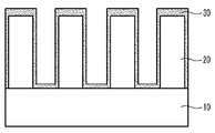
도 4는 본 발명의 일 실시예에 따른 프라이버시 보호 필터의 제조 과정에 있어서, 제1 투명 기판 위에 요철 패턴을 형성하는 방법을 나타내는 모식도이다.
도 5는 본 발명의 일 실시예에 따른 프라이버시 보호 필터의 제조 과정에 있어서, 상기 도 4에서 형성된 상기 요철 패턴 상에 제1 투명 도전막을 형성하는 방법을 나타내는 모식도이다.
도 6a는 본 발명의 일 실시예에 따른 프라이버시 보호 필터의 제조 과정에 있어서, 상기 도 5에서 형성된 제1 투명 도전막 위에 전기변색층을 형성하는 방법을 나타내는 모식도이다.
도 6b는 본 발명의 일 실시예에 따른 프라이버시 보호 필터의 제조 과정에 있어서, 상기 도 6a에서 형성된 구조에서 전기변색층의 일부를 건식 식각하는 방법을 나타내는 모식도이다.
도 7은 본 발명의 일 실시예에 따른 프라이버시 보호 필터의 제조 과정에 있어서, 상기 도 6b에서 형성된 구조와 제2 투명 기판을 이용한 프라이버시 필터를 제조하는 방법을 나타내는 모식도이다.
도 8은 본 발명의 실시예 1에 따라 제조된 프라이버시 보호 필터의 사진을 나타낸 것이다.
12: 제2 투명 기판
20: 고단차의 요철 패턴
30: 제1 투명 도전막
32: 제2 투명 도전막
40: 전기 변색층
50: 전해질
60: 스페이서
A: 요철 패턴의 선격자 폭
B: 요철 패턴의 트렌치 폭
C: 요철 패턴의 트렌치 깊이
a: 요철 패턴의 선격자의 제1 투명 도전막의 상부 부분
b: 요철 패턴의 트렌치 하부의 제1 투명 도전막 윗 부분
Claims (22)
- 제1 투명 기판과, 상기 제1 투명 기판에 대하여 일정 간격을 두고 서로 마주보도록 배치되는 제2 투명 기판과, 상기 제1 투명 기판 및 제2 투명 기판 사이에 충전된 전해질과, 상기 전해질 및 제2 투명 기판 사이의 제2 투명 도전막을 포함하며,
상기 제1 투명 기판은
상기 제1 투명 기판 위에 형성된 선격자 및 트렌치를 갖는 요철 패턴,
상기 요철 패턴의 선격자 및 트렌치 상에 형성된 제1 투명 도전막,
상기 선격자의 벽면을 따라 제1 투명 도전막 위에 형성되며, 전기의 인가 여부에 따라 가시광선을 투과 또는 흡수하는 전기변색물질을 함유하는 전기 변색층
을 포함하는 프라이버시 보호 필터. - 제1항에 있어서, 상기 전기 변색층은 요철 패턴의 선격자의 상부 및 트렌치 하부의 제1 투명 도전막 위에 더 포함하는 프라이버시 보호 필터.
- 제1항에 있어서, 상기 전기 변색층이 프러시안 블루 또는 전이금속 산화물을 포함하는 무기물인 프라이버시 보호 필터.
- 제3항에 있어서, 상기 전기 변색층이 프러시안 블루인 프라이버시 보호 필터.
- 제3항에 있어서, 상기 전기 변색층이 WO3 또는 LiNiO2인 전이금속 산화물로 이루어진 프라이버시 보호 필터.
- 제1항에 있어서, 상기 요철 패턴은 선격자 및 트렌치 폭이 10 ㎛ 이하이고, 하기 수학식 1로 표시되는 트렌치 가로세로비가 최소 2 이상인 패턴 구조를 가지는 프라이버시 보호 필터.
[수학식 1]
트렌치 가로세로비 = 트렌치 깊이/ 트렌치 폭 - 제1항에 있어서, 상기 요철 패턴은 감광제로부터 형성된 절연층인 프라이버시 보호 필터.
- 제1항에 있어서, 상기 전기 변색층은 두께가 10nm 내지 1 ㎛인 프라이버시 보호 필터.
- 제1항에 있어서, 상기 제1 투명 도전막은 요철 패턴의 선격자 및 트렌치 내부에서 벽면 두께가 20nm 내지 200nm인 프라이버시 보호 필터.
- 제1항에 있어서, 상기 제1 투명 도전막 및 제2 투명 도전막은 전도성 금속박막, ITO, FTO 및 ZnO로 이루어진 군에서 선택된 것인 프라이버시 보호 필터.
- 제1항에 있어서, 상기 제1 투명 기판 및 제2 투명 기판은 투명 유리, 폴리머 필름 또는 투명 플라스틱 기판인 프라이버시 보호 필터.
- 제1항에 있어서, 상기 보호 필터는 제1 투명 기판과 제2 투명기판을 고정하기 위한 스페이서를 더 포함하는 프라이버시 보호 필터.
- (a) 제1 투명 기판 위에 선격자 및 트렌치를 갖는 요철 패턴을 형성하는 단계;
(b) 상기 요철 패턴 상에 제1 투명 도전막을 형성하는 단계;
(c) 상기 요철 패턴의 제1 투명 도전막 위에 전기 변색층을 형성하는 단계;
(d) 제2 투명 도전막이 형성된 제2 투명 기판을 이용하여, 상기 (c)단계에서 형성된 기판과 제2 투명 기판 사이에 스페이서를 위치시키고, 전해액을 주입한 후 두 기판을 합착 및 밀봉하는 단계
를 포함하는 프라이버시 보호 필터의 제조방법. - 제13항에 있어서, 상기 방법은
상기 (c)단계의 제1 투명 도전막에 전기 변색층을 형성하는 단계 이후에, 상기 선격자 상부 및 트렌치 하부의 제1 투명 도전막 위에 형성된 전기 변색층을 건식 식각하는 단계를 더 포함하는 제조방법. - 제14항에 있어서, 상기 건식 식각은 유도결합 반응성 이온 식각을 사용하는 제조방법.
- 제13항에 있어서, 상기 (c) 전기 변색층을 형성하는 단계는
30 내지 60 μA/㎠의 전류 밀도 조건에서 전기 증착법을 사용하여 프러시안 블루 또는 전이금속 함유 화합물을 형성하는 단계를 포함하는 제조방법. - 제13항에 있어서, 상기 (a) 요철 패턴을 형성하는 단계에서,
포토리소그래피법, 마스터 몰드 방법 또는 물리적 가공방법을 사용하여 제1 투명 기판에 요철 패턴을 형성하는 단계를 포함하는 제조방법. - 제17항에 있어서, 상기 요철 패턴을 형성하는 단계에서, 포토리소그래피법은 제1 투명 기판 위에 절연층 형성용 물질을 코팅하고 마스크 노광하여 패턴을 형성하는 단계를 포함하는 제조방법.
- 제17항에 있어서, 상기 요철 패턴을 형성하는 단계에서, 마스터 몰드를 이용하여 필름을 복제하여 요철패턴을 형성하는 제조방법.
- 제17항에 있어서, 상기 요철 패턴을 형성하는 단계에서, 물리적 가공방법은 제1 투명 기판을 레이저 또는 기계적으로 가공하여 요철 패턴을 형성하는 제조방법.
- 제13항에 있어서, 상기 전해액은 0.2M 내지 2M 농도의 KCl 수용액, HCl 수용액 및 LiClO4-프로필렌 카보네이트 용액으로 이루어진 군에서 선택된 어느 하나 이상을 사용하는, 제조방법.
- 제 1 항의 프라이버시 보호 필터를 포함하는 디스플레이 소자.
Priority Applications (5)
| Application Number | Priority Date | Filing Date | Title |
|---|---|---|---|
| KR1020100037568A KR101226226B1 (ko) | 2010-04-22 | 2010-04-22 | 프라이버시 보호필터 및 그 제조방법 |
| JP2013504843A JP5512880B2 (ja) | 2010-04-22 | 2011-04-22 | プライバシー保護フィルター及びその製造方法 |
| CN201180031272.2A CN102947742B (zh) | 2010-04-22 | 2011-04-22 | 隐私保护滤光片及其制造方法 |
| US13/642,351 US9459472B2 (en) | 2010-04-22 | 2011-04-22 | Privacy filter comprising a wire grid |
| PCT/KR2011/002954 WO2011132992A2 (ko) | 2010-04-22 | 2011-04-22 | 프라이버시 보호필터 및 그 제조방법 |
Applications Claiming Priority (1)
| Application Number | Priority Date | Filing Date | Title |
|---|---|---|---|
| KR1020100037568A KR101226226B1 (ko) | 2010-04-22 | 2010-04-22 | 프라이버시 보호필터 및 그 제조방법 |
Publications (2)
| Publication Number | Publication Date |
|---|---|
| KR20110118020A KR20110118020A (ko) | 2011-10-28 |
| KR101226226B1 true KR101226226B1 (ko) | 2013-01-28 |
Family
ID=44834691
Family Applications (1)
| Application Number | Title | Priority Date | Filing Date |
|---|---|---|---|
| KR1020100037568A Active KR101226226B1 (ko) | 2010-04-22 | 2010-04-22 | 프라이버시 보호필터 및 그 제조방법 |
Country Status (5)
| Country | Link |
|---|---|
| US (1) | US9459472B2 (ko) |
| JP (1) | JP5512880B2 (ko) |
| KR (1) | KR101226226B1 (ko) |
| CN (1) | CN102947742B (ko) |
| WO (1) | WO2011132992A2 (ko) |
Cited By (3)
| Publication number | Priority date | Publication date | Assignee | Title |
|---|---|---|---|---|
| KR20150127211A (ko) * | 2013-03-13 | 2015-11-16 | 쓰리엠 이노베이티브 프로퍼티즈 컴파니 | 전자적 스위칭가능 프라이버시 디바이스 |
| KR20180084333A (ko) | 2017-01-16 | 2018-07-25 | 서울과학기술대학교 산학협력단 | 광학필름 및 이를 이용한 디스플레이 장치 |
| KR20190026502A (ko) | 2017-09-05 | 2019-03-13 | 주식회사 네이션스 | 광시야각 모드와 협시야각 모드의 스위칭이 가능한 디스플레이 장치용 사생활 보호 장치 |
Families Citing this family (40)
| Publication number | Priority date | Publication date | Assignee | Title |
|---|---|---|---|---|
| JP5924561B2 (ja) * | 2012-11-28 | 2016-05-25 | 株式会社村田製作所 | 視野角制御装置 |
| KR101589635B1 (ko) * | 2013-11-07 | 2016-02-01 | 한국과학기술연구원 | 마이크로 패터닝된 투명 도전성 금속 산화막을 포함하는 전기변색 창호 및 이의 제조방법 |
| CN103698958B (zh) * | 2013-12-24 | 2016-07-06 | 合肥京东方光电科技有限公司 | 一种信息保密屏及保密眼镜 |
| KR102090176B1 (ko) * | 2014-01-24 | 2020-03-17 | 한국전자통신연구원 | 주름 구조의 전극, 이를 포함하는 표시 장치 및 이의 제조 방법 |
| KR20150121533A (ko) * | 2014-04-21 | 2015-10-29 | 엄성우 | 시야간섭패턴을 이용한 프라이버시 필름과 그 제조방법 |
| CN103955017B (zh) * | 2014-04-21 | 2016-06-01 | 上海兆九光电技术有限公司 | 滤光片 |
| KR101645363B1 (ko) * | 2014-07-25 | 2016-08-04 | 주식회사 미뉴타텍 | 디스플레이용 광학 필름 및 그의 제조방법 |
| US9547202B2 (en) | 2014-12-19 | 2017-01-17 | Industrial Technology Research Institute | Transparent display panel |
| TWI576626B (zh) * | 2014-12-19 | 2017-04-01 | 財團法人工業技術研究院 | 顯示裝置 |
| US9547213B2 (en) | 2014-12-19 | 2017-01-17 | Industrial Technology Research Institute | Display device |
| WO2016137453A1 (en) * | 2015-02-25 | 2016-09-01 | Hewlett-Packard Development Company, L.P. | Electronic displays |
| DE102015011933B3 (de) * | 2015-09-14 | 2017-02-02 | Sioptica Gmbh | Verfahren und Verwendung eines Bildschirms zur sicheren Darstellung von Information |
| CN108027528A (zh) | 2015-09-23 | 2018-05-11 | 皇家飞利浦有限公司 | 显示设备和驱动方法 |
| JP6829969B2 (ja) * | 2015-09-28 | 2021-02-17 | 日東電工株式会社 | 光学部材、ならびに、該光学部材を用いた偏光板のセットおよび液晶表示装置 |
| WO2017111943A1 (en) * | 2015-12-22 | 2017-06-29 | Hewlett-Packard Development Company, L.P. | Privacy and light absorption in display device |
| KR102547026B1 (ko) * | 2016-07-01 | 2023-06-27 | 삼성디스플레이 주식회사 | 표시장치 및 그 제조 방법 |
| US10444410B2 (en) | 2016-08-16 | 2019-10-15 | Moxtek, Inc. | Overcoat wire grid polarizer having conformal coat layer with oxidation barrier and moisture barrier |
| CN109983369B (zh) * | 2016-11-22 | 2022-03-08 | 3M创新有限公司 | 角度和光谱选择性检测器和光源系统 |
| US11640019B2 (en) * | 2016-11-22 | 2023-05-02 | 3M Innovative Properties Company | Spectrally selective retroreflective system |
| CN109983370B (zh) * | 2016-11-22 | 2022-01-25 | 3M创新有限公司 | 具有光谱选择性的光控膜 |
| WO2018097873A1 (en) * | 2016-11-22 | 2018-05-31 | Moxtek, Inc. | Overcoat wire grid polarizer |
| KR102078402B1 (ko) | 2017-04-27 | 2020-02-17 | 주식회사 엘지화학 | 전기변색소자 |
| EP3731010B1 (en) * | 2017-12-20 | 2023-09-27 | Boe Technology Group Co., Ltd. | Visibility range adjustment component and driving method therefor, visibility range adjustment apparatus, and display apparatus |
| KR102467612B1 (ko) * | 2017-12-27 | 2022-11-15 | 엘지디스플레이 주식회사 | 프라이버시 보호 필름 및 이를 포함하는 표시 장치 |
| KR102485839B1 (ko) * | 2017-12-27 | 2023-01-05 | 엘지디스플레이 주식회사 | 프라이버시 보호 필름 및 이를 포함하는 표시 장치 |
| USD844626S1 (en) | 2018-03-12 | 2019-04-02 | 3M Innovative Properties Company | Privacy filter with mounting tape for electronic display device |
| USD844625S1 (en) | 2018-03-12 | 2019-04-02 | 3M Innovative Properties Company | Privacy filter with mounting tape for electronic display device |
| USD844624S1 (en) | 2018-03-12 | 2019-04-02 | 3M Innovative Properties Company | Privacy filter with mounting tape for electronic display device |
| US20210116771A1 (en) * | 2018-04-17 | 2021-04-22 | Applied Materials, Inc. | Privacy application device, method for operation thereof, and system including a privacy application device |
| CN112005163A (zh) * | 2018-07-02 | 2020-11-27 | 惠普发展公司,有限责任合伙企业 | 具有成角度聚合物分散液晶通道的屏保密性设备 |
| US11397366B2 (en) | 2018-08-10 | 2022-07-26 | E Ink California, Llc | Switchable light-collimating layer including bistable electrophoretic fluid |
| KR102521144B1 (ko) | 2018-08-10 | 2023-04-12 | 이 잉크 캘리포니아 엘엘씨 | 쌍안정 전기영동 유체를 포함하는 전환가능한 광 시준층에 대한 구동 파형들 |
| CN112470067B (zh) | 2018-08-10 | 2025-04-18 | 伊英克公司 | 具有反射器的可切换的光准直层 |
| US11402716B2 (en) * | 2018-12-07 | 2022-08-02 | Beijing Boe Optoelectronics Technology Co., Ltd. | Visual range adjustment component and driving method thereof, visual range adjustment device, and display device |
| TWI680328B (zh) * | 2018-12-11 | 2019-12-21 | 友達光電股份有限公司 | 顯示裝置及其製造方法 |
| US12174407B2 (en) * | 2018-12-11 | 2024-12-24 | 3M Innovative Properties Company | Light control film |
| CN111627319B (zh) * | 2020-05-26 | 2024-11-01 | 深圳市真屏科技发展有限公司 | 防窥膜 |
| JP7504731B2 (ja) | 2020-09-10 | 2024-06-24 | 株式会社ジャパンディスプレイ | 視野角制御素子及び表示装置 |
| JP7473997B2 (ja) | 2020-09-30 | 2024-04-24 | ジオプティカ・ゲゼルシャフト・ミット・ベシュレンクテル・ハフツング | 切替え可能な光フィルタとその使用 |
| KR20220128551A (ko) | 2021-03-12 | 2022-09-21 | 삼성디스플레이 주식회사 | 표시 장치 |
Citations (2)
| Publication number | Priority date | Publication date | Assignee | Title |
|---|---|---|---|---|
| KR20080001522A (ko) * | 2006-06-29 | 2008-01-03 | 엘지.필립스 엘시디 주식회사 | 시야각 제어가 가능한 액정 표시 장치 및 그의 제조 방법 |
| KR20080051280A (ko) * | 2006-12-05 | 2008-06-11 | 주식회사 엘지화학 | 전기변색소자용 전극 및 이를 구비한 전기변색소자 |
Family Cites Families (14)
| Publication number | Priority date | Publication date | Assignee | Title |
|---|---|---|---|---|
| JPS5365096A (en) * | 1976-11-24 | 1978-06-10 | Citizen Watch Co Ltd | Electrochemical luminescence display device |
| JPS6081044A (ja) * | 1983-10-11 | 1985-05-09 | Toyoda Gosei Co Ltd | ガラス板 |
| JP2980882B2 (ja) | 1998-04-08 | 1999-11-22 | ウシオ電機株式会社 | 高圧水銀ランプ |
| WO2002048803A1 (en) | 2000-12-14 | 2002-06-20 | Ttools, Llc | Holographic privacy filter for display device |
| US20090009852A1 (en) * | 2001-05-15 | 2009-01-08 | E Ink Corporation | Electrophoretic particles and processes for the production thereof |
| JP3675752B2 (ja) * | 2001-10-24 | 2005-07-27 | 信越ポリマー株式会社 | 情報表示体用の覗き見防止体 |
| FR2840078B1 (fr) * | 2002-05-22 | 2004-08-13 | Saint Gobain | Dispositif electrocommandable a proprietes optiques et/ou energetiques variables |
| FR2882828B1 (fr) * | 2005-03-03 | 2007-04-06 | Saint Gobain | Procede d'alimentation d'un dispositif electrocommandable a proprietes optiques et/ou energetiques variables |
| JP4382791B2 (ja) * | 2006-05-16 | 2009-12-16 | Nec液晶テクノロジー株式会社 | 光線方向制御素子の製造方法 |
| US8115984B2 (en) * | 2007-06-18 | 2012-02-14 | Ajjer Llc | Laminated electrochromic devices and processes for forming the same |
| KR20090063369A (ko) * | 2007-12-14 | 2009-06-18 | 삼성전자주식회사 | 컬러 표시 장치 |
| US8072671B2 (en) * | 2007-12-26 | 2011-12-06 | Industrial Technology Research Institute | Display device |
| US8622691B2 (en) | 2008-01-28 | 2014-01-07 | Ihi Corporation | Supercharger |
| KR101091533B1 (ko) * | 2008-01-29 | 2011-12-13 | 주식회사 엘지화학 | 시야각 제한 필름의 제조 방법 |
-
2010
- 2010-04-22 KR KR1020100037568A patent/KR101226226B1/ko active Active
-
2011
- 2011-04-22 CN CN201180031272.2A patent/CN102947742B/zh active Active
- 2011-04-22 WO PCT/KR2011/002954 patent/WO2011132992A2/ko active Application Filing
- 2011-04-22 US US13/642,351 patent/US9459472B2/en active Active
- 2011-04-22 JP JP2013504843A patent/JP5512880B2/ja active Active
Patent Citations (2)
| Publication number | Priority date | Publication date | Assignee | Title |
|---|---|---|---|---|
| KR20080001522A (ko) * | 2006-06-29 | 2008-01-03 | 엘지.필립스 엘시디 주식회사 | 시야각 제어가 가능한 액정 표시 장치 및 그의 제조 방법 |
| KR20080051280A (ko) * | 2006-12-05 | 2008-06-11 | 주식회사 엘지화학 | 전기변색소자용 전극 및 이를 구비한 전기변색소자 |
Cited By (4)
| Publication number | Priority date | Publication date | Assignee | Title |
|---|---|---|---|---|
| KR20150127211A (ko) * | 2013-03-13 | 2015-11-16 | 쓰리엠 이노베이티브 프로퍼티즈 컴파니 | 전자적 스위칭가능 프라이버시 디바이스 |
| KR102183001B1 (ko) * | 2013-03-13 | 2020-11-25 | 쓰리엠 이노베이티브 프로퍼티즈 컴파니 | 전자적 스위칭가능 프라이버시 디바이스 |
| KR20180084333A (ko) | 2017-01-16 | 2018-07-25 | 서울과학기술대학교 산학협력단 | 광학필름 및 이를 이용한 디스플레이 장치 |
| KR20190026502A (ko) | 2017-09-05 | 2019-03-13 | 주식회사 네이션스 | 광시야각 모드와 협시야각 모드의 스위칭이 가능한 디스플레이 장치용 사생활 보호 장치 |
Also Published As
| Publication number | Publication date |
|---|---|
| JP2013524293A (ja) | 2013-06-17 |
| WO2011132992A2 (ko) | 2011-10-27 |
| JP5512880B2 (ja) | 2014-06-04 |
| US20130050798A1 (en) | 2013-02-28 |
| CN102947742A (zh) | 2013-02-27 |
| KR20110118020A (ko) | 2011-10-28 |
| WO2011132992A3 (ko) | 2012-03-08 |
| CN102947742B (zh) | 2015-04-22 |
| US9459472B2 (en) | 2016-10-04 |
Similar Documents
| Publication | Publication Date | Title |
|---|---|---|
| KR101226226B1 (ko) | 프라이버시 보호필터 및 그 제조방법 | |
| KR101127277B1 (ko) | 전기변색소자용 전극 및 이를 구비한 전기변색소자 | |
| CN103472648B (zh) | 一种电致变色器件及其制作方法和显示装置 | |
| EP3076227B1 (en) | Transmittance-variable film and method for producing same | |
| JP2010108684A (ja) | 透明導電性基板、及び電気化学表示素子 | |
| WO2021121172A1 (zh) | 一种电致变色器件及其制备方法和应用 | |
| CN113066604B (zh) | 一种导电膜及制备方法 | |
| CN103838044B (zh) | 基板及其制造方法、显示装置 | |
| CN108803112A (zh) | 双面液晶显示面板、双面显示器 | |
| KR102102204B1 (ko) | 광시야각 모드와 협시야각 모드의 스위칭이 가능한 디스플레이 장치용 사생활 보호 장치 | |
| CN108628051A (zh) | 光学元件 | |
| KR101480950B1 (ko) | 셀 구조 일렉트로크로믹 소자 및 이의 제조 방법 | |
| EP3731010B1 (en) | Visibility range adjustment component and driving method therefor, visibility range adjustment apparatus, and display apparatus | |
| WO2009119221A1 (ja) | 帯電粒子移動型表示パネルの製造方法、帯電粒子移動型表示パネル及び帯電粒子移動型表示装置 | |
| CN108873400A (zh) | 显示装置及宽窄视角显示方法 | |
| WO2015010362A1 (zh) | 一种电致变色显示面板及其制备方法、显示装置 | |
| CN116300237A (zh) | 一种基于复合电极的大尺寸电致变色器件及制备方法 | |
| CN102890381B (zh) | 一种电致变色器件及其制备方法 | |
| CN203386178U (zh) | 滤光片模块及使用该滤光片模块的触摸显示屏 | |
| KR101480951B1 (ko) | 매립형 일렉트로크로믹 소자 및 그 제조 방법 | |
| CN203338307U (zh) | 偏光滤光模块及触摸显示屏 | |
| KR20180136726A (ko) | 전기변색소자 | |
| CN203338311U (zh) | 滤光片组件及使用该滤光片组件的触摸显示屏 | |
| CN103365472A (zh) | 偏光滤光模块及触摸显示屏 | |
| CN203338296U (zh) | 滤光片组件及使用该滤光片组件的触摸显示屏 |
Legal Events
| Date | Code | Title | Description |
|---|---|---|---|
| PA0109 | Patent application |
Patent event code: PA01091R01D Comment text: Patent Application Patent event date: 20100422 |
|
| A201 | Request for examination | ||
| PA0201 | Request for examination |
Patent event code: PA02012R01D Patent event date: 20111004 Comment text: Request for Examination of Application Patent event code: PA02011R01I Patent event date: 20100422 Comment text: Patent Application |
|
| PG1501 | Laying open of application | ||
| PE0902 | Notice of grounds for rejection |
Comment text: Notification of reason for refusal Patent event date: 20121011 Patent event code: PE09021S01D |
|
| E701 | Decision to grant or registration of patent right | ||
| PE0701 | Decision of registration |
Patent event code: PE07011S01D Comment text: Decision to Grant Registration Patent event date: 20121227 |
|
| GRNT | Written decision to grant | ||
| PR0701 | Registration of establishment |
Comment text: Registration of Establishment Patent event date: 20130118 Patent event code: PR07011E01D |
|
| PR1002 | Payment of registration fee |
Payment date: 20130118 End annual number: 3 Start annual number: 1 |
|
| PG1601 | Publication of registration | ||
| FPAY | Annual fee payment |
Payment date: 20151229 Year of fee payment: 4 |
|
| PR1001 | Payment of annual fee |
Payment date: 20151229 Start annual number: 4 End annual number: 4 |
|
| FPAY | Annual fee payment |
Payment date: 20161227 Year of fee payment: 5 |
|
| PR1001 | Payment of annual fee |
Payment date: 20161227 Start annual number: 5 End annual number: 5 |
|
| FPAY | Annual fee payment |
Payment date: 20180116 Year of fee payment: 6 |
|
| PR1001 | Payment of annual fee |
Payment date: 20180116 Start annual number: 6 End annual number: 6 |
|
| FPAY | Annual fee payment |
Payment date: 20190116 Year of fee payment: 7 |
|
| PR1001 | Payment of annual fee |
Payment date: 20190116 Start annual number: 7 End annual number: 7 |
|
| FPAY | Annual fee payment |
Payment date: 20200116 Year of fee payment: 8 |
|
| PR1001 | Payment of annual fee |
Payment date: 20200116 Start annual number: 8 End annual number: 8 |
|
| PR1001 | Payment of annual fee |
Payment date: 20210118 Start annual number: 9 End annual number: 9 |
|
| PR1001 | Payment of annual fee |
Payment date: 20220117 Start annual number: 10 End annual number: 10 |
|
| PR1001 | Payment of annual fee |
Payment date: 20221226 Start annual number: 11 End annual number: 11 |
|
| PR1001 | Payment of annual fee |
Payment date: 20231226 Start annual number: 12 End annual number: 12 |
|
| PR1001 | Payment of annual fee |
Payment date: 20241219 Start annual number: 13 End annual number: 13 |