KR101140376B1 - Process chamber for manufacturing substrate - Google Patents
Process chamber for manufacturing substrate Download PDFInfo
- Publication number
- KR101140376B1 KR101140376B1 KR1020110048236A KR20110048236A KR101140376B1 KR 101140376 B1 KR101140376 B1 KR 101140376B1 KR 1020110048236 A KR1020110048236 A KR 1020110048236A KR 20110048236 A KR20110048236 A KR 20110048236A KR 101140376 B1 KR101140376 B1 KR 101140376B1
- Authority
- KR
- South Korea
- Prior art keywords
- nozzle
- substrate
- unit
- spray
- spray nozzle
- Prior art date
Links
- 239000000758 substrate Substances 0.000 title claims abstract description 474
- 238000004519 manufacturing process Methods 0.000 title claims abstract description 163
- 238000000034 method Methods 0.000 title claims description 297
- 239000007921 spray Substances 0.000 claims abstract description 254
- 239000007788 liquid Substances 0.000 claims abstract description 147
- 238000005507 spraying Methods 0.000 claims abstract description 35
- 238000002347 injection Methods 0.000 claims description 119
- 239000007924 injection Substances 0.000 claims description 119
- 238000004140 cleaning Methods 0.000 claims description 66
- 239000000243 solution Substances 0.000 claims description 62
- 238000005530 etching Methods 0.000 claims description 51
- 229920002120 photoresistant polymer Polymers 0.000 claims description 22
- 238000011161 development Methods 0.000 claims description 14
- 238000012545 processing Methods 0.000 abstract description 5
- 238000012546 transfer Methods 0.000 description 68
- 238000001035 drying Methods 0.000 description 19
- XLYOFNOQVPJJNP-UHFFFAOYSA-N water Chemical compound O XLYOFNOQVPJJNP-UHFFFAOYSA-N 0.000 description 13
- 240000006829 Ficus sundaica Species 0.000 description 11
- 230000033001 locomotion Effects 0.000 description 10
- 230000005540 biological transmission Effects 0.000 description 7
- KFZMGEQAYNKOFK-UHFFFAOYSA-N Isopropanol Chemical compound CC(C)O KFZMGEQAYNKOFK-UHFFFAOYSA-N 0.000 description 6
- HEMHJVSKTPXQMS-UHFFFAOYSA-M Sodium hydroxide Chemical compound [OH-].[Na+] HEMHJVSKTPXQMS-UHFFFAOYSA-M 0.000 description 6
- VEXZGXHMUGYJMC-UHFFFAOYSA-N Hydrochloric acid Chemical compound Cl VEXZGXHMUGYJMC-UHFFFAOYSA-N 0.000 description 4
- QAOWNCQODCNURD-UHFFFAOYSA-N Sulfuric acid Chemical compound OS(O)(=O)=O QAOWNCQODCNURD-UHFFFAOYSA-N 0.000 description 4
- 239000000356 contaminant Substances 0.000 description 4
- 239000000463 material Substances 0.000 description 4
- WGTYBPLFGIVFAS-UHFFFAOYSA-M tetramethylammonium hydroxide Chemical compound [OH-].C[N+](C)(C)C WGTYBPLFGIVFAS-UHFFFAOYSA-M 0.000 description 4
- QTBSBXVTEAMEQO-UHFFFAOYSA-N Acetic acid Chemical compound CC(O)=O QTBSBXVTEAMEQO-UHFFFAOYSA-N 0.000 description 3
- 238000000206 photolithography Methods 0.000 description 3
- 229920000139 polyethylene terephthalate Polymers 0.000 description 3
- 239000005020 polyethylene terephthalate Substances 0.000 description 3
- 239000000126 substance Substances 0.000 description 3
- QGZKDVFQNNGYKY-UHFFFAOYSA-N Ammonia Chemical compound N QGZKDVFQNNGYKY-UHFFFAOYSA-N 0.000 description 2
- MHAJPDPJQMAIIY-UHFFFAOYSA-N Hydrogen peroxide Chemical compound OO MHAJPDPJQMAIIY-UHFFFAOYSA-N 0.000 description 2
- 239000008367 deionised water Substances 0.000 description 2
- 229910021641 deionized water Inorganic materials 0.000 description 2
- 230000000694 effects Effects 0.000 description 2
- 238000005516 engineering process Methods 0.000 description 2
- 239000011521 glass Substances 0.000 description 2
- AMGQUBHHOARCQH-UHFFFAOYSA-N indium;oxotin Chemical compound [In].[Sn]=O AMGQUBHHOARCQH-UHFFFAOYSA-N 0.000 description 2
- 239000004973 liquid crystal related substance Substances 0.000 description 2
- 239000011859 microparticle Substances 0.000 description 2
- 239000000203 mixture Substances 0.000 description 2
- -1 polyethylene terephthalate Polymers 0.000 description 2
- 238000000926 separation method Methods 0.000 description 2
- 238000004904 shortening Methods 0.000 description 2
- KRHYYFGTRYWZRS-UHFFFAOYSA-N Fluorane Chemical compound F KRHYYFGTRYWZRS-UHFFFAOYSA-N 0.000 description 1
- BQCADISMDOOEFD-UHFFFAOYSA-N Silver Chemical compound [Ag] BQCADISMDOOEFD-UHFFFAOYSA-N 0.000 description 1
- 229910021529 ammonia Inorganic materials 0.000 description 1
- 238000006243 chemical reaction Methods 0.000 description 1
- 238000001514 detection method Methods 0.000 description 1
- 238000005108 dry cleaning Methods 0.000 description 1
- 238000005401 electroluminescence Methods 0.000 description 1
- 238000001704 evaporation Methods 0.000 description 1
- 238000004299 exfoliation Methods 0.000 description 1
- 239000012530 fluid Substances 0.000 description 1
- 239000007789 gas Substances 0.000 description 1
- 229910000040 hydrogen fluoride Inorganic materials 0.000 description 1
- 230000001678 irradiating effect Effects 0.000 description 1
- 238000012986 modification Methods 0.000 description 1
- 230000004048 modification Effects 0.000 description 1
- 230000001151 other effect Effects 0.000 description 1
- 239000004065 semiconductor Substances 0.000 description 1
- 229910052709 silver Inorganic materials 0.000 description 1
- 239000004332 silver Substances 0.000 description 1
- 238000006467 substitution reaction Methods 0.000 description 1
- 238000005406 washing Methods 0.000 description 1
Images


Classifications
-
- G—PHYSICS
- G03—PHOTOGRAPHY; CINEMATOGRAPHY; ANALOGOUS TECHNIQUES USING WAVES OTHER THAN OPTICAL WAVES; ELECTROGRAPHY; HOLOGRAPHY
- G03F—PHOTOMECHANICAL PRODUCTION OF TEXTURED OR PATTERNED SURFACES, e.g. FOR PRINTING, FOR PROCESSING OF SEMICONDUCTOR DEVICES; MATERIALS THEREFOR; ORIGINALS THEREFOR; APPARATUS SPECIALLY ADAPTED THEREFOR
- G03F1/00—Originals for photomechanical production of textured or patterned surfaces, e.g., masks, photo-masks, reticles; Mask blanks or pellicles therefor; Containers specially adapted therefor; Preparation thereof
- G03F1/60—Substrates
-
- G—PHYSICS
- G03—PHOTOGRAPHY; CINEMATOGRAPHY; ANALOGOUS TECHNIQUES USING WAVES OTHER THAN OPTICAL WAVES; ELECTROGRAPHY; HOLOGRAPHY
- G03F—PHOTOMECHANICAL PRODUCTION OF TEXTURED OR PATTERNED SURFACES, e.g. FOR PRINTING, FOR PROCESSING OF SEMICONDUCTOR DEVICES; MATERIALS THEREFOR; ORIGINALS THEREFOR; APPARATUS SPECIALLY ADAPTED THEREFOR
- G03F7/00—Photomechanical, e.g. photolithographic, production of textured or patterned surfaces, e.g. printing surfaces; Materials therefor, e.g. comprising photoresists; Apparatus specially adapted therefor
- G03F7/16—Coating processes; Apparatus therefor
-
- G—PHYSICS
- G03—PHOTOGRAPHY; CINEMATOGRAPHY; ANALOGOUS TECHNIQUES USING WAVES OTHER THAN OPTICAL WAVES; ELECTROGRAPHY; HOLOGRAPHY
- G03F—PHOTOMECHANICAL PRODUCTION OF TEXTURED OR PATTERNED SURFACES, e.g. FOR PRINTING, FOR PROCESSING OF SEMICONDUCTOR DEVICES; MATERIALS THEREFOR; ORIGINALS THEREFOR; APPARATUS SPECIALLY ADAPTED THEREFOR
- G03F7/00—Photomechanical, e.g. photolithographic, production of textured or patterned surfaces, e.g. printing surfaces; Materials therefor, e.g. comprising photoresists; Apparatus specially adapted therefor
- G03F7/20—Exposure; Apparatus therefor
- G03F7/2041—Exposure; Apparatus therefor in the presence of a fluid, e.g. immersion; using fluid cooling means
-
- H—ELECTRICITY
- H01—ELECTRIC ELEMENTS
- H01L—SEMICONDUCTOR DEVICES NOT COVERED BY CLASS H10
- H01L21/00—Processes or apparatus adapted for the manufacture or treatment of semiconductor or solid state devices or of parts thereof
- H01L21/02—Manufacture or treatment of semiconductor devices or of parts thereof
- H01L21/027—Making masks on semiconductor bodies for further photolithographic processing not provided for in group H01L21/18 or H01L21/34
- H01L21/0271—Making masks on semiconductor bodies for further photolithographic processing not provided for in group H01L21/18 or H01L21/34 comprising organic layers
- H01L21/0273—Making masks on semiconductor bodies for further photolithographic processing not provided for in group H01L21/18 or H01L21/34 comprising organic layers characterised by the treatment of photoresist layers
- H01L21/0274—Photolithographic processes
-
- H—ELECTRICITY
- H01—ELECTRIC ELEMENTS
- H01L—SEMICONDUCTOR DEVICES NOT COVERED BY CLASS H10
- H01L21/00—Processes or apparatus adapted for the manufacture or treatment of semiconductor or solid state devices or of parts thereof
- H01L21/02—Manufacture or treatment of semiconductor devices or of parts thereof
- H01L21/04—Manufacture or treatment of semiconductor devices or of parts thereof the devices having potential barriers, e.g. a PN junction, depletion layer or carrier concentration layer
- H01L21/18—Manufacture or treatment of semiconductor devices or of parts thereof the devices having potential barriers, e.g. a PN junction, depletion layer or carrier concentration layer the devices having semiconductor bodies comprising elements of Group IV of the Periodic Table or AIIIBV compounds with or without impurities, e.g. doping materials
- H01L21/30—Treatment of semiconductor bodies using processes or apparatus not provided for in groups H01L21/20 - H01L21/26
- H01L21/302—Treatment of semiconductor bodies using processes or apparatus not provided for in groups H01L21/20 - H01L21/26 to change their surface-physical characteristics or shape, e.g. etching, polishing, cutting
Landscapes
- Physics & Mathematics (AREA)
- General Physics & Mathematics (AREA)
- Engineering & Computer Science (AREA)
- Condensed Matter Physics & Semiconductors (AREA)
- Manufacturing & Machinery (AREA)
- Computer Hardware Design (AREA)
- Microelectronics & Electronic Packaging (AREA)
- Power Engineering (AREA)
- Weting (AREA)
Abstract
Description
본 발명은 기판 제조용 공정 챔버에 관한 것으로, 보다 상세하게는 기판 제조용 공정 챔버의 구조를 단순화 및 소형화하고, 기판 제조 공정의 생산성 및 효율성을 향상시킬 수 있는 기판 제조용 공정 챔버에 관한 것이다.The present invention relates to a substrate manufacturing process chamber, and more particularly, to a substrate manufacturing process chamber capable of simplifying and miniaturizing the structure of the substrate manufacturing process chamber and improving productivity and efficiency of the substrate manufacturing process.
일반적으로 반도체 제조 공정, 터치 패널(Touch Panel), LCD(Liquid crystal display)와 같은 평판표시장치(Flat panel display, FPD) 등을 제조하기 위해서는 기판(Substrate) 상에 소정의 패턴들을 형성해야 하는데, 이러한 패턴들을 형성하기 위해서는 포토리소그래피(photolithography) 기술을 적용할 수 있다. 여기서 기판(Substrate)은 특정 형상의 패턴(Pattern)이 형성된 ITO(Indium Tin Oxide) 필름 등의 투명 전도막과 이에 연결되는 배선이 형성된 PET(Polyethylene Terephthalate) 필름 또는 글래스(Glass) 등을 의미한다.In general, in order to manufacture a flat panel display (FPD) such as a semiconductor manufacturing process, a touch panel, a liquid crystal display (LCD), predetermined patterns must be formed on a substrate. To form such patterns, photolithography technology may be applied. Here, the substrate refers to a transparent conductive film such as an indium tin oxide (ITO) film having a pattern of a specific shape and a polyethylene terephthalate (PET) film or glass having a wire connected thereto.
일반적으로 잘 알려진 포토리소그래피(photolithography) 기술은 기판에 도포된 포토레지스트(Photoresist)에 포토 마스크(Photo mask)를 정렬한 후 노광(Exposure) 및 현상(Develop) 공정(이하, 현상 공정), 식각(Etching) 공정 및 박리(Strip) 공정을 순차적으로 수행하여 원하는 패턴을 가진 기판을 형성할 수 있다. 또한, 각각의 여러 단계의 공정을 수행하는 과정에서 기판에 부착된 각종 오염물을 제거하기 위한 공정으로 공정액(Chemical) 또는 순수(Deionized Water)를 이용한 세정(Wet Cleaning, Rinse) 공정이 있다. 이러한 포토레지스트의 도포, 현상, 식각, 박리, 세정 공정 등에서는 액체 상태의 공정액 또는 순수를 기판 위로 분사시켜 공정이 이루어진다.Generally known photolithography techniques align the photo mask with a photoresist applied to the substrate, followed by an exposure, development, and etching processes. Etching) and stripping processes may be sequentially performed to form a substrate having a desired pattern. In addition, there is a process for removing various contaminants attached to the substrate in the process of performing each of the various steps, such as a wet cleaning or rinse process using chemical or deionized water. In the application, development, etching, peeling, and cleaning processes of the photoresist, a process is performed by spraying a liquid process liquid or pure water onto a substrate.
일반적으로 기판을 제조하기 위한 일련의 공정을 수행하는 기판 제조 장치는 웨이퍼(Wafer)와 같은 기판을 회전시키고 회전하는 기판 위로 공정액을 분사하여 각각의 공정을 수행하는 스핀 장치의 구조나, LCD 등과 같은 평판표시장치(Flat Panel Display, FPD)의 제조 장치와 마찬가지로 벨트 및 풀리로 이루어진 컨베이어 형태의 이송 장치를 이용하는 구조를 가졌다.In general, a substrate manufacturing apparatus that performs a series of processes for manufacturing a substrate has a structure of a spin apparatus that performs a respective process by rotating a substrate such as a wafer and spraying a process liquid onto the rotating substrate, or an LCD, or the like. Like a flat panel display (FPD) manufacturing apparatus has a structure using a conveyor-type transfer device consisting of a belt and a pulley.
그러나, 종래의 기판 제조 장치는 기판의 제조에 필요한 각각의 공정을 별개의 공정 챔버에서 수행하였다. 즉, 기판을 제조하기 위해 현상 공정, 식각 공정, 박리 공정, 세정 공정 등을 수행하기 위한 공정 챔버를 따로 구비하고, 기판 이송 장치를 이용하여 기판을 각각의 공정 챔버로 순차적으로 이송하여 일련의 공정을 수행하였다. 따라서, 전체적으로 기판 제조 장치의 크기가 대형화되고, 각각의 공정 챔버로의 기판의 순차적인 이송으로 인해 전체 공정 시간이 늘어났으며, 각각의 공정 챔버에서 사용되는 공정액의 사용량이 증가한다는 문제점이 있었다.However, the conventional substrate manufacturing apparatus performed each process required for the manufacture of the substrate in a separate process chamber. That is, a process chamber for performing a developing process, an etching process, a peeling process, a cleaning process, and the like is separately prepared to manufacture a substrate, and the substrate is transferred to each process chamber sequentially using a substrate transfer device to sequentially process the substrate. Was performed. Therefore, the overall size of the substrate manufacturing apparatus is increased, the overall process time is increased due to the sequential transfer of the substrate to each process chamber, and the amount of the process liquid used in each process chamber is increased. .
따라서, 기판 제조용 공정 챔버의 구조를 단순화 및 소형화하고, 기판 제조 공정의 생산성 및 효율성을 향상시킬 수 있는 기판 제조용 공정 챔버가 요구된다.Therefore, there is a need for a substrate manufacturing process chamber capable of simplifying and miniaturizing the structure of the substrate manufacturing process chamber and improving productivity and efficiency of the substrate manufacturing process.
본 발명은 상기한 문제점을 개선하기 위해 발명된 것으로, 본 발명이 해결하고자 하는 과제는, 복수의 공정액을 분사하는 분사 노즐부를 교대로 기판의 상부면으로 이송하여 복수의 공정액을 순차적으로 분사하여 기판을 제조하기 위한 일련의 공정을 하나의 공정 챔버 내에서 수행함으로써, 기판 제조용 공정 챔버의 구조를 단순화 및 소형화하고, 기판 제조 공정의 생산성 및 효율성을 향상시킬 수 있는 기판 제조용 공정 챔버를 제공하는 것이다.The present invention has been invented to improve the above problems, and the problem to be solved by the present invention is to sequentially spray the plurality of process liquids by sequentially transferring the injection nozzle unit for spraying a plurality of process liquids to the upper surface of the substrate By performing a series of processes for manufacturing a substrate in one process chamber, thereby simplifying and miniaturizing the structure of the substrate manufacturing process chamber, and providing a substrate manufacturing process chamber capable of improving the productivity and efficiency of the substrate manufacturing process. will be.
본 발명의 기술적 과제는 이상에서 언급한 것들로 제한되지 않으며, 언급되지 않은 또 다른 기술적 과제는 아래의 기재로부터 당업자에게 명확하게 이해될 수 있을 것이다.The technical problem of the present invention is not limited to those mentioned above, and another technical problem which is not mentioned can be clearly understood by those skilled in the art from the following description.
상기 과제를 달성하기 위하여, 본 발명의 일 실시예에 따른 기판 제조용 공정 챔버는, 기판(Substrate)을 제조하기 위한 기판 제조 장치에 구비되며, 일 측에 형성된 개구부를 통해 내부로 반입된 상기 기판에 대해 상기 기판을 제조하기 위한 복수의 공정을 순차적으로 수행한 후 상기 개구부를 통해 상기 복수의 공정을 마친 상기 기판을 반출하는 기판 제조용 공정 챔버에 있어서, 기판(Substrate)을 지지하고 회전시키는 기판 지지부 및 일단은 상기 기판을 제조하기 위한 복수의 공정에 사용되는 복수의 공정액 중 적어도 하나의 공정액을 분사하기 위한 적어도 하나의 노즐 분사구가 구비되고, 타단은 상기 기판 지지부의 일 측에 수평 방향으로 회전하거나 수직 방향으로 이동 가능하게 설치되는 적어도 하나의 분사 노즐부를 포함하고, 상기 적어도 하나의 분사 노즐부는, 상기 적어도 하나의 공정액을 분사하기 위한 적어도 하나의 노즐 분사구가 구비된 노즐 헤드(Nozzle Head)와, 상기 기판 지지부의 일 측에 설치되고, 일단은 상기 노즐 헤드가 연결되며, 타단은 상기 기판 지지부의 일 측에서 수평 방향으로 회전하거나 수직 방향으로 이동 가능하게 연결되는 노즐 헤드 지지부 및 상기 노즐 헤드 지지부의 타단에 연결되어 상기 노즐 헤드 지지부를 수평 방향으로 회전시키는 노즐 헤드 회전 구동부와, 상기 노즐 헤드 회전 구동부의 일 측에 연결되어 상기 노즐 헤드 회전 구동부를 수직 방향으로 이동시키는 노즐 헤드 승강 구동부를 구비하여, 상기 노즐 헤드 지지부를 수평 방향으로 회전시키거나 수직 방향으로 이동시키는 구동력을 제공하는 노즐 헤드 구동부를 포함하며, 상기 적어도 하나의 분사 노즐부는, 상기 기판 지지부에 의해 회전하는 상기 기판의 상부면을 향해 상기 기판에 도포된 포토레지스트(Photoresist)에 소정의 패턴(Pattern)을 형성하기 위한 현상(Develop) 공정에 사용되는 현상액과, 상기 현상 공정을 마친 상기 기판으로부터 상기 소정의 패턴에 해당하는 부분의 포토레지스트를 부식시키기 위한 식각(Etching) 공정에 사용되는 식각액과, 상기 식각 공정을 마친 상기 기판에 잔존하는 포토레지스트를 제거하기 위한 박리(Strip) 공정에 사용되는 박리액 및 상기 박리 공정을 마친 상기 기판을 세정하기 위한 린스(Rinse) 공정에 사용되는 린스액을 순차적으로 분사하는 것을 특징으로 한다.In order to achieve the above object, the substrate manufacturing process chamber according to an embodiment of the present invention, which is provided in the substrate manufacturing apparatus for manufacturing a substrate (Substrate), to the substrate carried in through the opening formed in one side A substrate support process chamber for carrying out a plurality of processes for manufacturing the substrate in sequence and then carrying out the substrate after the plurality of processes through the opening, the substrate support portion for supporting and rotating the substrate (Substrate) and One end is provided with at least one nozzle injection port for injecting at least one process liquid of a plurality of process liquids used in a plurality of processes for manufacturing the substrate, the other end is rotated in a horizontal direction on one side of the substrate support Or at least one spray nozzle part installed to be movable in the vertical direction, wherein the at least one The injection nozzle unit is provided with a nozzle head having at least one nozzle injection hole for injecting the at least one process liquid and one side of the substrate support, one end of which is connected to the nozzle head, and the other end. A nozzle head rotation driving unit connected to a nozzle head support part rotatably connected in a horizontal direction or movable in a vertical direction on one side of the substrate support part and the other end of the nozzle head support part to rotate the nozzle head support part in a horizontal direction; A nozzle head lifting drive unit connected to one side of the nozzle head rotation driving unit to move the nozzle head rotation driving unit in a vertical direction to provide a driving force to rotate the nozzle head support unit in a horizontal direction or to move in a vertical direction A nozzle head drive, wherein the at least one spray nozzle Is a developer used in a development process for forming a predetermined pattern in a photoresist applied to the substrate toward an upper surface of the substrate rotated by the substrate support, and the development Etching liquid used in an etching process for corroding the photoresist of the portion corresponding to the predetermined pattern from the finished substrate and exfoliation for removing the photoresist remaining on the substrate after the etching process ( Stripping liquid used in the strip) process and the rinse liquid used in the rinse (Rinse) process for cleaning the substrate after the peeling process is characterized in that the spraying sequentially.
삭제delete
기타 실시예들의 구체적인 사항들은 상세한 설명 및 도면들에 포함되어 있다.Specific details of other embodiments are included in the detailed description and the drawings.
본 발명의 일 실시예에 따른 기판 제조용 공정 챔버에 따르면, 기판 지지부를 회전 지지판을 적어도 하나의 리브를 가지는 얇은 원판 형상으로 구현함으로써, 회전 지지판의 재료를 절약할 수 있을 뿐 아니라 회전 지지판의 경량화를 통해 전체적으로 기판 제조용 공정 챔버의 구조를 단순화하고 소형화시킬 수 있다. 또한, 기판의 하부면 또는 측면을 지지하는 복수의 지지핀을 구비함으로써, 기판의 지지를 확실히 할 수 있으므로, 기판 제조 공정의 생산성 및 효율성을 향상시킬 수 있다.According to the process chamber for manufacturing a substrate according to an embodiment of the present invention, by implementing the substrate support portion in a thin disk shape having at least one rib, the material of the rotary support plate can be reduced and the weight of the rotary support plate can be reduced. Through this, the structure of the process chamber for manufacturing a substrate can be simplified and miniaturized. In addition, since the support of the substrate can be ensured by providing a plurality of support pins that support the lower surface or the side surface of the substrate, the productivity and efficiency of the substrate manufacturing process can be improved.
또한, 본 발명의 일 실시예에 따른 기판 제조용 공정 챔버에 따르면, 분사 노즐부의 노즐 헤드 구동부를 노즐 헤드가 구비된 노즐 암을 수평 방향으로 회전시키는 노즐 헤드 회전 구동부와, 노즐 헤드 회전 구동부를 수직 방향으로 이동시키는 노즐 헤드 승강 구동부로 구성함으로써, 노즐 암의 수평 회전 또는 수직 이동을 안정적으로 할 수 있고, 기판 제조용 공정 챔버의 구조를 단순화하고 소형화시킬 수 있다.In addition, according to the process chamber for manufacturing a substrate according to an embodiment of the present invention, the nozzle head drive unit for rotating the nozzle head with the nozzle head in the horizontal direction, the nozzle head drive unit of the injection nozzle unit, and the nozzle head rotation drive unit in the vertical direction By configuring the nozzle head lift drive unit to move in the horizontal direction, the horizontal rotation or vertical movement of the nozzle arm can be made stable, and the structure of the process chamber for manufacturing a substrate can be simplified and downsized.
또한, 본 발명의 일 실시예에 따른 기판 제조용 공정 챔버에 따르면, 복수의 공정액을 분사하는 적어도 하나의 분사 노즐부를 교대로 기판의 상부면으로 이동하여, 현상액, 식각액, 박리액 및 린스액을 순차적으로 분사할 수 있으므로, 기판을 제조하기 위한 일련의 공정을 하나의 공정 챔버 내에서 수행할 수 있다. 따라서, 전체적으로 터치 패널 제조 장치를 소형화하고, 기판의 이송 거리를 최소화하여 터치 패널 공정 시간을 단축시키고 공정액 사용량을 최소화하여 터치 패널 제조 공정의 효율성을 향상시킬 수 있다.In addition, according to the process chamber for manufacturing a substrate according to an embodiment of the present invention, the developer, the etching solution, the peeling liquid and the rinse liquid are alternately moved to the upper surface of the substrate by alternately spraying at least one spray nozzle part for spraying a plurality of process liquids. Since it can be sprayed sequentially, a series of processes for manufacturing the substrate can be performed in one process chamber. Therefore, the overall size of the touch panel manufacturing apparatus can be reduced, the transfer distance of the substrate can be minimized, the touch panel manufacturing time can be shortened, and the amount of the process solution can be minimized, thereby improving the efficiency of the touch panel manufacturing process.
본 발명의 효과들은 이상에서 언급한 효과들로 제한되지 않으며, 언급되지 않은 또 다른 효과들은 청구범위의 기재로부터 당업자에게 명확하게 이해될 수 있을 것이다.The effects of the present invention are not limited to the effects mentioned above, and other effects not mentioned can be clearly understood by those skilled in the art from the description of the claims.
도 1은 기판을 제조하기 위한 기판 제조 장치의 일 예로서 터치 패널을 제조하기 위한 터치 패널 제조 장치의 구조를 나타내는 평면도이다.
도 2는 도 1의 터치 패널 제조 장치에서 기판 이송부의 구조를 나타내는 사시도이다.
도 3 및 도 4는 본 발명의 일 실시예에 따른 기판 제조용 공정 챔버의 외부 구조를 나타내는 사시도이다.
도 5는 본 발명의 일 실시예에 따른 기판 제조용 공정 챔버의 내부 구조를 나타내는 사시도이다.
도 6은 본 발명의 일 실시예에 따른 기판 제조용 공정 챔버에서 기판 지지부의 구조를 나타내는 사시도이다.
도 7은 본 발명의 일 실시예에 따른 기판 제조용 공정 챔버에서 기판 지지부의 구조를 나타내는 분해 사시도이다.
도 8은 본 발명의 일 실시예에 따른 기판 제조용 공정 챔버에서 분사 노즐부의 구조를 나타내는 사시도이다.
도 9는 본 발명의 일 실시예에 따른 기판 제조용 공정 챔버의 분사 노즐부에서 노즐 헤드의 구조를 나타내는 측면도이다.
도 10은 본 발명의 일 실시예에 따른 기판 제조용 공정 챔버의 분사 노즐부에서 노즐 헤드 구동부의 구조를 나타내는 사시도이다.
도 11은 본 발명의 일 실시예에 따른 기판 제조용 공정 챔버에서 기판 지지부에 기판이 로딩되는 상태를 나타내는 평면도이다.
도 12는 본 발명의 일 실시예에 따른 기판 제조용 공정 챔버에서 제1 분사 노즐부가 공정액을 분사하는 상태를 나타내는 평면도이다.
도 13은 본 발명의 일 실시예에 따른 기판 제조용 공정 챔버에서 제2 분사 노즐부가 공정액을 분사하는 상태를 나타내는 평면도이다.
도 14는 본 발명의 다른 실시예에 따른 기판 제조용 공정 챔버의 내부 구조를 나타내는 사시도이다.
도 15는 본 발명의 다른 실시예에 따른 기판 제조용 공정 챔버의 내부 구조를 나타내는 평면도이다.
도 16은 본 발명의 다른 실시예에 따른 기판 제조용 공정 챔버에서 기판 지지부에 기판이 로딩되는 상태를 나타내는 평면도이다.
도 17은 본 발명의 다른 실시예에 따른 기판 제조용 공정 챔버에서 제1 분사 노즐부와 제2 분사 노즐부가 공정액을 분사하는 상태를 나타내는 평면도이다.
도 18은 본 발명의 다른 실시예에 따른 기판 제조용 공정 챔버에서 제3 분사 노즐부와 제4 노즐부가 공정액을 분사하는 상태를 나타내는 평면도이다.
도 19는 본 발명의 다른 실시예에 따른 기판 제조용 공정 챔버에서 세정 노즐과 메가소닉 노즐이 세정 공정을 수행하는 상태를 나타내는 평면도이다.1 is a plan view illustrating a structure of a touch panel manufacturing apparatus for manufacturing a touch panel as an example of a substrate manufacturing apparatus for manufacturing a substrate.
FIG. 2 is a perspective view illustrating a structure of a substrate transfer unit in the touch panel manufacturing apparatus of FIG. 1.
3 and 4 are perspective views illustrating an external structure of a process chamber for manufacturing a substrate according to an embodiment of the present invention.
5 is a perspective view illustrating an internal structure of a process chamber for manufacturing a substrate according to an embodiment of the present invention.
6 is a perspective view showing the structure of the substrate support in the substrate manufacturing process chamber according to an embodiment of the present invention.
7 is an exploded perspective view illustrating a structure of a substrate support part in a process chamber for manufacturing a substrate according to an embodiment of the present invention.
8 is a perspective view illustrating a structure of an injection nozzle unit in a process chamber for manufacturing a substrate according to an embodiment of the present invention.
9 is a side view illustrating a structure of a nozzle head in an injection nozzle unit of a process chamber for manufacturing a substrate according to an embodiment of the present invention.
10 is a perspective view illustrating a structure of a nozzle head driving unit in an injection nozzle unit of a process chamber for manufacturing a substrate according to an embodiment of the present invention.
FIG. 11 is a plan view illustrating a state in which a substrate is loaded on a substrate support unit in a process chamber for manufacturing a substrate according to an embodiment of the present invention. FIG.
12 is a plan view illustrating a state in which a first spray nozzle unit sprays a process liquid in a process chamber for manufacturing a substrate according to an embodiment of the present invention.
FIG. 13 is a plan view illustrating a state in which a second spray nozzle unit sprays a process liquid in a process chamber for manufacturing a substrate according to an embodiment of the present disclosure. FIG.
14 is a perspective view illustrating an internal structure of a process chamber for manufacturing a substrate according to another embodiment of the present invention.
15 is a plan view illustrating an internal structure of a process chamber for manufacturing a substrate according to another embodiment of the present invention.
16 is a plan view illustrating a state in which a substrate is loaded in a substrate support unit in a process chamber for manufacturing a substrate according to another embodiment of the present invention.
17 is a plan view illustrating a state in which a first spray nozzle part and a second spray nozzle part spray a process liquid in a process chamber for manufacturing a substrate according to another embodiment of the present invention.
18 is a plan view illustrating a state in which the third spray nozzle unit and the fourth nozzle unit spray the process liquid in the process chamber for manufacturing a substrate according to another embodiment of the present invention.
19 is a plan view illustrating a state in which a cleaning nozzle and a megasonic nozzle perform a cleaning process in a substrate manufacturing process chamber according to another embodiment of the present invention.
이하, 본 발명이 속하는 기술 분야에서 통상의 지식을 가진 자가 본 발명을 용이하게 실시할 수 있을 정도로 본 발명의 바람직한 실시예를 첨부된 도면을 참조하여 상세하게 설명하면 다음과 같다.DETAILED DESCRIPTION OF THE PREFERRED EMBODIMENTS Hereinafter, preferred embodiments of the present invention will be described in detail with reference to the accompanying drawings, so that those skilled in the art can easily carry out the present invention.
실시예를 설명함에 있어서 본 발명이 속하는 기술 분야에 익히 알려져 있고 본 발명과 직접적으로 관련이 없는 기술 내용에 대해서는 설명을 생략한다. 이는 불필요한 설명을 생략함으로써 본 발명의 요지를 흐리지 않고 더욱 명확히 전달하기 위함이다.In describing the embodiments, descriptions of technical contents which are well known in the technical field to which the present invention belongs and are not directly related to the present invention will be omitted. This is to more clearly communicate without obscure the subject matter of the present invention by omitting unnecessary description.
마찬가지 이유로 첨부 도면에 있어서 일부 구성요소는 과장되거나 생략되거나 개략적으로 도시되었다. 또한, 각 구성요소의 크기는 실제 크기를 전적으로 반영하는 것이 아니다. 각 도면에서 동일한 또는 대응하는 구성요소에는 동일한 참조 번호를 부여하였다.For the same reason, some of the components in the drawings are exaggerated, omitted, or schematically illustrated. In addition, the size of each component does not fully reflect the actual size. The same or corresponding components in each drawing are given the same reference numerals.
이하, 본 발명의 실시예들에 의하여 기판 제조용 공정 챔버를 설명하기 위한 도면들을 참고하여 본 발명에 대해 설명하도록 한다.Hereinafter, the present invention will be described with reference to the drawings for describing a process chamber for manufacturing a substrate according to embodiments of the present invention.
도 1은 기판을 제조하기 위한 기판 제조 장치의 일 예로서 터치 패널을 제조하기 위한 터치 패널 제조 장치의 구조를 나타내는 평면도이다.1 is a plan view illustrating a structure of a touch panel manufacturing apparatus for manufacturing a touch panel as an example of a substrate manufacturing apparatus for manufacturing a substrate.
도 1에 도시된 바와 같이, 터치 패널(Touch Panel)을 제조하기 위한 터치 패널 제조 장치(1)는, 기판 로딩부(10), 기판 언로딩부(20), 기판 정렬부(30), 기판 이송부(40) 및 복수의 공정 챔버(100)를 포함하여 구성될 수 있다. 즉, 터치 패널 제조 장치(1)는 터치 패널을 제조하기 위해 터치 패널을 구성하는 기판(Substrate)(S)에 일련의 공정을 순차적으로 수행하기 위한 복수의 공정 챔버(Processing Chamber)(100)들로 구성될 수 있다. 본 명세서에서 기판(Substrate)(S)이란, 터치 패널을 제조하기 위해 특정 형상의 패턴(Pattern)이 형성된 ITO(Indium Tin Oxide) 필름 등의 투명 전도막과 이에 연결되는 배선이 형성된 PET(Polyethylene Terephthalate) 필름 또는 글래스(Glass) 등을 의미한다. 도 1에서는 기판(S)이 대략 정사각형의 얇은 판 형상을 가지는 예를 도시하고 있으나, 이에 한정되지 않고, 당업자에 의해 얼마든지 변경 가능하다.As shown in FIG. 1, the touch
먼저, 도 1을 참조하여, 터치 패널 제조 장치(1)를 구성하는 각각의 구성 요소들의 구조 및 기능을 간단히 설명하면 다음과 같다.First, referring to FIG. 1, the structure and function of each component constituting the touch
먼저, 기판 로딩부(10)는 기판(S)을 복수의 공정 챔버(100)로 이송하기 위해 복수의 기판(S)을 수용하고 있는 기판 수용부(도시되지 않음)로부터 기판(S)을 기판 이송부(40)로 로딩(Loading)할 수 있다. 또한, 기판 언로딩부(20)는 복수의 공정 챔버(100)로부터 모든 공정을 마친 기판(S)을 기판 이송부(40)로부터 복수의 기판(S)을 수용하기 위한 기판 수용부(도시되지 않음)로 언로딩(Unloading)할 수 있다. 기판 이송부(40)는 기판 로딩부(10)의 기판 수용부(도시되지 않음)에 적재된 복수의 기판(S)을 순차적으로 로딩하여 기판 제조 공정을 수행할 각각의 공정 챔버(100)로 이송하고, 모든 공정을 마친 기판(S)을 기판 언로딩부(20)의 기판 수용부(도시되지 않음)로 언로딩하여 순차적으로 적재할 수 있다. 도 1에 도시된 바와 같이, 기판 로딩부(10)와 기판 언로딩부(20)는 기판 이송부(40)의 일 측에 서로 인접하여 배치될 수 있으나, 이에 한정되지 않으며, 터치 패널 제조 장치(1)의 크기, 공정 속도 등을 고려하여 서로 분리되어 배치될 수도 있다.First, the
또한, 기판 정렬부(30)는 기판 로딩부(10)로부터 로딩된 기판(S) 또는 기판 언로딩부(20)로 언로딩(Unloading)되는 기판(S)의 위치를 정렬할 수 있다. 도 1에서는 기판 정렬부(30)가 기판 이송부(40)를 중심으로 기판 로딩부(10) 및 기판 언로딩부(20)의 맞은 편에 위치하고 있는 예를 도시하고 있으나, 기판 로딩부(10) 또는 기판 언로딩부(20)의 일 측에 위치할 수도 있다. 비록 도시되지는 않았으나, 기판 정렬부(30)의 내부에는 기판(S)의 하부면을 지지하기 위한 기판 지지핀과 기판(S)의 전후 및 좌우 측면을 안내하기 위한 복수의 가이드부를 가지는 기판 정렬 유닛이 설치될 수 있다.In addition, the
또한, 각각의 공정 챔버(100)는 터치 패널을 구성하는 기판(S)에 대해 노광(Exposure) 및 현상(Develop) 공정, 식각(Etching) 공정, 박리(Strip) 공정, 린스(Rinse) 공정(세정 공정) 및 건조(Drying) 공정을 순차적으로 수행할 수 있다. 즉, 각각의 공정 챔버(100)는 내부로 반입된 기판(S)에 대해 기판(S)을 제조하기 위한 모든 공정을 수행한 후 기판(S)을 외부로 반출할 수 있다. 이와 같이, 본 발명의 일 실시예에 따른 기판 제조용 공정 챔버(100)는 하나의 공정 챔버(100) 내에서 기판(S)을 제조하기 위한 모든 공정을 수행하도록 구성함으로써, 터치 패널 제조 장치(1)를 소형화하고 터치 패널 공정 시간을 단축시킬 수 있으므로, 터치 패널을 구성하는 기판(S)의 생산성 및 터치 패널 제조 공정의 효율성을 크게 향상시킬 수 있다.In addition, each
도 1에 도시된 바와 같이, 본 발명의 일 실시예에 따른 기판 제조용 공정 챔버(100)는 회전하는 기판(S) 상에 각각의 공정에 해당하는 공정액(Chemical)을 분사하여 해당 공정을 수행하는 스핀 장치의 형태를 가질 수 있다. 즉, 각각의 공정 챔버(100)는 기판(S)을 지지하여 회전시키는 기판 지지부와 해당 공정을 수행하기 위해 적어도 하나의 공정액을 기판(S)으로 분사하는 적어도 하나의 분사 노즐부를 포함할 수 있다. 이러한 복수의 공정 챔버(100)의 자세한 구조 및 동작에 대해서는 도 3 내지 도 10를 참조하여 자세히 후술하기로 한다.As shown in FIG. 1, the
마지막으로, 기판 이송부(40)는 기판 로딩부(10)로부터 로딩된 기판(S)을 기판 정렬부(30), 각각의 공정 챔버(100) 및 기판 언로딩부(20)로 순차적으로 이송할 수 있다. 도 1에 도시된 바와 같이, 기판 이송부(40)는 터치 패널 제조 장치(1)의 중앙부에 위치하며, 터치 패널 제조 장치(1)의 길이 방향을 따라 길게 배치될 수 있다.Finally, the
도 1에 도시된 바와 같이, 터치 패널 제조 장치(1)는 기판 로딩부(10), 기판 정렬부(30), 복수의 공정 챔버(100) 및 기판 언로딩부(20)가 기판 이송부(40)를 중심으로 서로 마주보도록 배치될 수 있다. 즉, 터치 패널 제조 장치(1)는 복수의 공정 챔버(100)들이 터치 패널 제조 장치(1)의 중앙부에 위치하는 기판 이송부(40)를 둘러 쌓은 트랙(Track) 장비의 형태로 배치된 구조를 가질 수 있다. 이와 같이, 터치 패널 제조 장치(1)를 트랙 장비의 형태로 구현하게 되면, 터치 패널 제조 장비의 크기를 전체적으로 소형화시킬 수 있고, 터치 패널의 이송 거리를 최소화하여 터치 패널 제조 공정의 효율성을 향상시킬 수 있다.As illustrated in FIG. 1, the touch
도 2는 도 1의 터치 패널 제조 장치에서 기판 이송부의 구조를 나타내는 사시도이다.FIG. 2 is a perspective view illustrating a structure of a substrate transfer unit in the touch panel manufacturing apparatus of FIG. 1.
도 2에 도시된 바와 같이, 기판 이송부(40)는 크게 이송 로봇(41)과 이송 로봇 구동부(42)를 포함하여 구성될 수 있다. 이송 로봇(41)은 몸체(41a)에 수평 방향으로 회전 가능하게 결합되고 몸체(41a)를 중심으로 수축 또는 팽창되도록 동작하는 적어도 하나의 암(Arm)(41b)과, 적어도 하나의 암(41b) 각각의 일 측에 구비되어 기판(S)을 수평으로 지지하는 블레이드(Blade)(41c)를 구비할 수 있다. 또한, 이송 로봇 구동부(42)는 터치 패널 제조 장치(1)의 길이 방향을 따라 길게 형성된 베이스 판(42a)에 구비된 가이드 레일(42b) 상에서 이송 로봇(41)을 수평 방향으로 이송시킴으로써, 이송 로봇(41)은 기판(S)을 원하는 공정 챔버로 이송시킬 수 있다. 이송 로봇 구동부(42)는 이송 로봇(41)을 이송시키기 위해 베이스 판(42a)의 일 측에 길이 방향을 따라 길게 설치된 리니어 모터(Linear motor)와 같은 액츄에이터(42c)를 구비할 수 있다.As shown in FIG. 2, the
도 2에서는 기판 이송부(40)가 2 개의 암(41b)을 구비한 하나의 이송 로봇(41)을 포함하는 예를 도시하고 있으나, 이에 한정되지 않으며, 터치 패널 제조 장치(1)의 크기, 공정 속도 등을 고려하여 복수의 이송 로봇을 구비할 수 있다. 또한, 도 3에서는 이송 로봇 구동부(42)가 터치 패널 제조 장치(1)의 길이 방향을 따라 이송 로봇(41)을 직선 이동시키는 예로 들고 있으나, 이송 로봇 구동부(42)의 구조는 이에 한정되지 않으며, 터치 패널 제조 장치(1)의 크기, 공정 속도 등을 고려하여 이송 로봇 구동부(42)가 터치 패널 제조 장치(1)의 중앙부에서 이송 로봇(41)을 회전 이동시키도록 구현될 수도 있다.2 illustrates an example in which the
이하, 도 3 내지 도 10을 참조하여, 본 발명의 일 실시예에 따른 기판 제조용 공정 챔버의 구조를 자세히 설명하면 다음과 같다.3 to 10, the structure of a substrate manufacturing process chamber according to an embodiment of the present invention will be described in detail as follows.
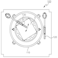
도 3 및 도 4는 본 발명의 일 실시예에 따른 기판 제조용 공정 챔버의 외부 구조를 나타내는 사시도이고, 도 5는 본 발명의 일 실시예에 따른 기판 제조용 공정 챔버의 내부 구조를 나타내는 사시도이다.3 and 4 are perspective views showing the external structure of the substrate manufacturing process chamber according to an embodiment of the present invention, Figure 5 is a perspective view showing the internal structure of the substrate manufacturing process chamber according to an embodiment of the present invention.
도 3 및 도 4에 도시된 바와 같이, 각각의 공정 챔버(100)는 복수의 파이프 등으로 공정 챔버(100) 전체의 골격을 형성하는 프레임 본체(101), 프레임 본체(101)의 상하부 측면에 구비된 복수의 작업 도어(102), 프레임 본체(101)의 일 측에 형성되어 기판(S)의 출입구 역할을 하는 슬릿 밸브(Slit Valve)(103) 및 프레임 본체(101)의 상부에 설치되어 팬(Fan)과 필터(Filter)를 이용해 공기를 순환시키는 팬 필터 유닛(Fan Filter Unit, FFU)(104)으로 구성될 수 있다. 슬릿 밸브(103)는 기판 이송부(40)를 바라보는 프레임 본체(101)의 일 측에 형성되며, 상하로 구동하여 공정 챔버(100)를 개폐할 수 있다. 즉, 기판 이송부(40)가 일련의 공정을 수행할 기판을 공정 챔버(100)의 내부로 반입하거나 일련의 공정을 마친 기판을 공정 챔버(100)의 외부로 반출할 때에는 슬릿 밸브(103)는 열린 상태가 되고, 공정 챔버(100)에서 일련의 공정이 수행될 때에는 슬릿 밸브(103)는 닫힌 상태가 될 수 있다.As shown in FIGS. 3 and 4, each of the
도 5에 도시된 바와 같이, 본 발명의 일 실시예에 따른 기판 제조용 공정 챔버(100)는 회전하는 기판(S) 상에 각각의 공정에 해당하는 공정액(Chemical)을 분사하여 해당 공정을 수행하는 스핀 장치의 형태를 가질 수 있으며, 크게 기판 지지부(110)와 적어도 하나의 분사 노즐부(120, 130)를 포함하여 구성될 수 있다.As shown in FIG. 5, the
먼저, 기판 지지부(110)는 대략 공정 챔버(100)의 중앙부에 위치하고, 기판 이송부(40)에 의해 공정 챔버(100)의 내부로 반입된 기판(S)을 지지하고 회전시킬 수 있다.First, the
도 6은 본 발명의 일 실시예에 따른 기판 제조용 공정 챔버에서 기판 지지부의 구조를 나타내는 사시도이고, 도 7은 본 발명의 일 실시예에 따른 기판 제조용 공정 챔버에서 기판 지지부의 구조를 나타내는 분해 사시도이다.6 is a perspective view illustrating a structure of a substrate support in a substrate manufacturing process chamber according to an embodiment of the present invention, and FIG. 7 is an exploded perspective view illustrating a structure of a substrate support in a substrate manufacturing process chamber according to an embodiment of the present invention. .
도 6 및 도 7에 도시된 바와 같이, 기판 지지부(110)는, 회전 지지판(111), 복수의 지지핀(112), 회전 지지판 구동부(113), 스핀 컵(114) 및 스핀 컵 구동부(115)를 포함하여 구성될 수 있다.As illustrated in FIGS. 6 and 7, the
회전 지지판(111)은 공정 챔버(100)의 중앙부에 회전 가능하도록 설치되고, 대략 얇은 원판 형상을 가질 수 있다. 도 7에 도시된 바와 같이, 회전 지지판(111)은 후술할 회전 지지판 구동부(113)에 결합되는 중심부로부터 복수의 리브(Rib)(111a)가 형성된 얇은 환(環) 형상을 가짐으로써, 회전 지지판(111)의 재료를 절약하고 회전 지지판(111)의 무게를 줄일 수 있을 뿐만 아니라, 회전 지지판(111) 전체의 응력이나 변형을 적게 할 수 있어 회전 지지판(111)의 내구성 및 안정성을 향상시킬 수도 있다.The
복수의 지지핀(112)은 회전 지지판(111)의 상부면에 고정되고, 기판(S)의 하부면 또는 측면을 지지할 수 있다. 도 7에 도시된 바와 같이, 복수의 지지핀(112)은 기판(S)의 하부면을 지지하는 복수의 하부 지지핀(112a)과 기판(S)의 측면을 지지하는 복수의 측부 지지핀(112b)으로 구성될 수 있다. 하부 지지핀(112a)은 대략 원통 형상으로 형성되고, 일단은 기판(S)의 하부면에 접촉하도록 돔(Dome) 형상으로 형성될 수 있다. 또한, 측부 지지핀(112b)은 대략 원통 형상으로 형성되어 기판(S)의 가장자리에 접촉하며, 기판(S)의 가장자리의 하부면을 지지하도록 접촉단이 형성될 수 있다. 도 5에 도시된 바와 같이, 기판(S)이 대략 정사각형의 얇은 판 형상을 가지는 경우에는, 측부 지지핀(112b)은 기판(S)의 네 모서리의 측면을 지지할 수 있도록 각 모서리마다 2 개씩 모두 8개가 구비될 수 있다. 한편, 도 6 및 도 7에서는 8 개의 하부 지지핀(112a)과 8 개의 측부 지지핀(112b)이 회전 지지판(111)의 상부면에 고정된 예를 도시하고 있으나, 이에 한정되지 않으며, 하부 지지핀(112a) 및 측부 지지핀(112b)의 개수 및 고정 위치는 당업자에 의해 얼마든지 변경 가능하다. 이와 같이, 본 발명의 일 실시예에 따른 기판 제조용 공정 챔버(100)의 경우, 기판(S)의 하부면 또는 측면을 지지하는 복수의 지지핀(112)을 구비함으로써, 가판(S)의 지지를 확실히 할 수 있으므로, 기판 제조 공정의 정확성 및 효율성을 향상시킬 수 있다.The plurality of support pins 112 may be fixed to the upper surface of the
한편, 도 7에 도시된 바와 같이, 회전 지지판 구동부(113)는 회전 지지판(111)의 중심부에 연결되며, 회전 지지판(111)을 회전 구동시킬 수 있다. 회전 지지판 구동부(113)는 서보 모터와 같은 구동 모터로부터 발생된 회전력을 구동 샤프트를 통해 회전 지지판(111)으로 전달할 수 있다. 도 7에 도시된 회전 지지판 구동부(113)의 구조는 예시적인 것으로서, 이에 한정되지 않으며, 당업자에 의해 얼마든지 변경 가능하다. 또한, 도 7에서는 회전 지지판(111)이 수평 방향으로 회전 운동만 하는 구조를 예를 들어 설명하고 있으나, 회전 지지판(111)을 상하로 이동시키는 별도의 구동 장치가 연결될 수도 있다.On the other hand, as shown in Figure 7, the rotary support
스핀 컵(Spin cup)(114)은 상부면이 개방되고 회전 지지판(111)의 주위를 감싸도록 대략 원통 형상을 가지는 외벽이 형성되어 기판(S)이 수용되는 공간을 제공함으로써, 분사 노즐부(120, 130)에 의해 기판(S)으로 분사되는 복수의 공정액이 외부의 다른 장치나 주위로 튀어 나가 비산되는 현상을 방지할 수 있다. 이 때, 스핀 컵(114)은 해당 공정에 사용된 복수의 공정액을 모아 스핀 컵(114)의 하단에 연결된 배출구(도시되지 않음)를 통해 외부로 배출시킬 수 있다. 한편, 도 6에 도시된 바와 같이, 스핀 컵(114)의 내부에는 기판(S)의 하부면을 향해 공정액을 분사하는 적어도 하나의 하부 노즐(114a)이 설치될 수 있다. 적어도 하나의 분사 노즐부(120, 130)와 적어도 하나의 하부 노즐(114a)은 동시에 또는 순차적으로 기판(S)의 상부면 또는 하부면에 공정액 또는 세정액을 분사할 수 있다.The
스핀 컵 구동부(115)는 스핀 컵(114)의 하부 또는 측면에 연결되며, 스핀 컵(114)을 상하 방향으로 이동시킬 수 있다. 스핀 컵 구동부(115)는 기판 이송부(40)에 의해 반입된 기판(S)을 복수의 회전 지지핀(120)에 안착한 후 스핀 컵(114)을 상승시켜 박리 공정을 수행할 수 있도록 하고, 기판 이송부(40)가 박리 공정을 마친 기판(S)을 반출할 때에 스핀 컵(114)을 하강시킬 수 있다. 도 5에 도시된 바와 같이, 스핀 컵 구동부(115)로는 공압 실린더와 같은 적어도 하나의 액츄에이터(151)와 동력 전달 샤프트(152)를 사용할 수 있다.The
한편, 스핀 컵(114)의 상부면에는 기판(S)의 위치를 감지하여 기판(S)이 정위치에 놓여졌는지 여부를 판단하는 적어도 하나의 위치 감지 센서(116)가 설치될 수 있다. 여기서, 기판(S)의 정위치란 각종 공정을 수행하기 위해 기판 지지부(110) 상에서 기판(S)이 놓여지도록 정해진 위치를 의미한다. 위치 감지 센서(116)로는 포토 센서(Photo Sensor) 등을 사용할 수 있다.Meanwhile, at least one
이와 같이, 본 발명의 일 실시예에 따른 기판 제조용 공정 챔버(100)의 기판 지지부(110)는 회전 지지판(111)을 적어도 하나의 리브(111a)를 가지는 얇은 원판 형상으로 구현함으로써, 회전 지지판(111)의 재료를 절약할 수 있을 뿐 아니라 회전 지지판(111)의 경량화를 통해 전체적으로 기판 제조용 공정 챔버(100)의 구조를 단순화하고 소형화시킬 수 있다. 또한, 기판(S)의 하부면 또는 측면을 지지하는 복수의 지지핀(112)을 구비함으로써, 기판(S)의 지지를 확실히 할 수 있으므로, 기판 제조 공정의 정확성 및 효율성을 향상시킬 수 있다.As such, the
한편, 도 6 및 도 7에 도시된 기판 지지부(110)의 구조는 예시적인 것으로서, 이에 한정되지 않고, 당업자에 의해 얼마든지 변경 가능하다.Meanwhile, the structure of the
다시 도 5를 참조하면, 본 발명의 일 실시예에 따른 기판 제조용 공정 챔버(100)는 제1 분사 노즐부(120) 및 제2 분사 노즐부(130)를 포함할 수 있다. 제1 분사 노즐부(120) 및 제2 분사 노즐부(130)는, 기판 지지부(110)에 인접하여 위치하며, 기판 지지부(110)에 의해 회전하는 기판(S)의 상부면으로 각각 해당 공정을 수행하기 위한 공정액을 분사할 수 있다. 이 때, 분사 노즐부(120, 130)에 의해 분사된 공정액은 회전하는 기판(S)의 회전력에 의해 상부면 전체로 퍼져 전체적으로 균일하게 해당 공정이 이루어질 수 있다. 제1 분사 노즐부(120) 및 제2 분사 노즐부(130)는 실질적으로 동일한 구조를 가질 수 있으므로, 제1 분사 노즐부(120)를 중심으로 분사 노즐부의 구조를 자세히 설명하기로 한다.Referring back to FIG. 5, the substrate
도 8은 본 발명의 일 실시예에 따른 기판 제조용 공정 챔버에서 분사 노즐부의 구조를 나타내는 사시도이고, 도 9는 본 발명의 일 실시예에 따른 기판 제조용 공정 챔버의 분사 노즐부에서 노즐 헤드의 구조를 나타내는 측면도이며, 도 10은 본 발명의 일 실시예에 따른 기판 제조용 공정 챔버의 분사 노즐부에서 노즐 헤드 구동부의 구조를 나타내는 사시도이다.8 is a perspective view illustrating a structure of a spray nozzle unit in a process chamber for manufacturing a substrate according to an embodiment of the present invention, and FIG. 9 illustrates a structure of a nozzle head in a spray nozzle unit of a process chamber for manufacturing a substrate according to an embodiment of the present invention. 10 is a perspective view illustrating a structure of a nozzle head driving unit in an injection nozzle unit of a process chamber for manufacturing a substrate according to an embodiment of the present invention.
도 8에 도시된 바와 같이, 제1 분사 노즐부(120)는 노즐 헤드(121), 노즐 헤드 지지부(122) 및 노즐 헤드 구동부(123, 124)를 포함하여 구성될 수 있다.As shown in FIG. 8, the first
노즐 헤드(Nozzle Head)(121)는 공정액을 분사하기 위한 적어도 하나의 노즐 분사구(121a)를 구비할 수 있다. 도 9에 도시된 바와 같이, 노즐 분사구(121a)는 회전 지지판(111)의 반지름 방향을 따라 복수 개가 일렬로 배치되어 노즐 헤드 블록(121b)에 고정될 수 있다. 노즐 헤드 블록(121b)의 상단에는 노즐 헤드 지지부(122)의 노즐 암(122a)의 내부에 형성된 공정액 공급관으로부터 공급되는 공정액을 노즐 분사구(121a)로 공급하는 공정액 공급 라인(121c)이 연결될 수 있다. 도시되지는 않았으나, 공정액 공급 라인(121c)을 통해 공급된 공정액은 노즐 헤드 블록(121b)의 내부에 형성된 경로를 따라 각각의 노즐 분사구(121a)로 분배될 수 있다. 도 9에서는 5 개의 노즐 분사구가 일렬로 배치된 예를 도시하고 있으나, 이에 한정되지 않으며, 노즐 분사구의 개수 및 배치 형태는 기판(S)의 면적, 회전 지지판(111)의 회전 속도 등을 고려하여 당업자에 의해 얼마든지 변경 가능하다.The
다시 도 8을 참조하면, 노즐 헤드 지지부(122)는 노즐 헤드(121)를 수직 또는 수평 방향으로 이동 가능하도록 베이스(105) 상에 고정 결합시킬 수 있다. 노즐 헤드 지지부(122)는 일단에 노즐 헤드(121)가 연결되고 수평 방향으로 길게 형성된 노즐 암(122a), 노즐 암(122a)의 타단을 지지하고 일 측으로 외부로부터 공정액이 유입되는 노즐 암 지지 블록(122b), 노즐 암 지지 블록(122b)의 하단으로부터 수직하게 형성되고 노즐 헤드 구동부(123, 124)에 연결되어 노즐 암(121a)를 수평 방향으로 회전시키거나 수직 방향으로 이동시키는 구동력을 전달하는 구동 샤프트(122c) 및 노즐 암 지지 블록(122b)의 하단으로부터 수직하게 형성되고 구동 샤프트(122c)의 수평 회전 또는 수직 이동을 안내하는 구동 샤프트 지지 블록(122d)를 포함하여 구성될 수 있다. 도시되지는 않았으나, 노즐 암(122a)의 내부에는 노즐 헤드(121)로 공정액을 공급하는 공정액 공급관이 형성됨으로써 제1 분사 노즐부(120)의 구조를 단순화하고 소형화시킬 수 있다. 또한, 구동 샤프트 지지 블록(122d)의 내부에는 구동 샤프트(122c)의 수평 회전 또는 수직 이동을 안내하는 구동 샤프트 베어링가 구비됨으로써 구동 샤프트(122c)가 안정적으로 수평 방향으로 회전하거나 수직 방향으로 이동할 수 있다.Referring back to FIG. 8, the
도 8에 도시된 바와 같이, 노즐 헤드 구동부(123, 124)는 노즐 헤드 지지부(122)의 타단, 보다 정확하게는 구동 샤프트(122c)의 타단에 연결되며, 노즐 헤드(121)가 연결된 노즐 암(112a)를 수평 방향으로 회전시키거나 수직 방향으로 이동시키는 구동력을 제공할 수 있다. 노즐 헤드 구동부(123, 124)는 이송 로봇 등과 같은 기판 이송부(40)에 의해 반입된 기판(S)이 기판 지지부(110)에 안착된 후 노즐 헤드(121)가 기판(S)의 상부면으로 공정액을 분사할 수 있도록 노즐 헤드(121)를 기판(S)의 상부면으로 위치시킬 수 있다. 또한, 노즐 헤드 구동부(123, 124)는 기판(S)이 기판 이송부(40)에 의해 반입 또는 반출될 때에 기판 이송부(40)의 이송 로봇과 간섭하지 않도록 노즐 헤드(121)를 위치시킬 수 있다.As shown in FIG. 8, the nozzle head drives 123 and 124 are connected to the other end of the
도 10에 도시된 바와 같이, 노즐 헤드 구동부(123, 124)는, 구동 샤프트(122c)의 타단에 연결되고 구동 샤프트(122c)를 수평 방향으로 회전시키는 노즐 헤드 회전 구동부(123) 및 노즐 헤드 회전 구동부(123)의 일 측에 연결되고 노즐 헤드 회전 구동부(123)를 수직 방향으로 이동시키는 노즐 헤드 승강 구동부(124)로 구성될 수 있다.As shown in FIG. 10, the nozzle head drives 123 and 124 are connected to the other end of the
도 10에 도시된 바와 같이, 노즐 헤드 회전 구동부(123)는, 회전력을 발생시키는 제1 구동 모터(123a), 일단은 구동 샤프트(122c)의 타단이 삽입 고정되고 타단은 제1 구동 모터(123a)가 연결되어 구동 샤프트(122c)로 제1 구동 모터(123a)의 회전력을 전달하는 회전 전달부(123b) 및 상단부에 회전 전달부(123b)가 회전 가능하게 결합되고, 하단부에 제1 구동 모터(123a)가 고정되며, 일 측에 형성된 체결부(도시되지 않음)를 통해 노즐 헤드 승강 구동부(124)에 결합되는 회전 구동부 고정 블록(123c)을 포함하여 구성될 수 있다. 한편, 도시되지는 않았으나, 회전 전달부(123b)의 일 측에는 구동 샤프트(122c)의 회전 각도를 감지하여 제어하기 위해 회전 감지 센서(도시되지 않음)가 설치될 수 있다.As shown in FIG. 10, the nozzle head
또한, 도 10에 도시된 바와 같이, 노즐 헤드 승강 구동부(124)는, 회전력을 발생시키는 제2 구동 모터(124a), 일 측에 회전 구동부 고정 블록(123c)이 결합되고 제2 구동 모터(124a)로부터 발생된 회전력을 직선 운동을 변환하여 회전 구동부 고정 블록(123c)을 상하로 이동시키는 동력 전달부(124b)로 구성될 수 있다. 자세히 도시되지는 않았으나, 동력 전달부(124b)는 제2 구동 모터(124a)로부터 발생된 회전력을 직선 운동을 변환하는 볼 스크류, 볼 스크류에 결합되어 볼 스크류의 회전에 따라 상하 방향으로의 직선 이동을 안내하는 적어도 하나의 슬라이딩 레일로 구성될 수 있다. 한편, 동력 전달부(124b)의 일 측에는 회전 구동부 고정 블록(123c)의 이동 위치를 감지하여 제어하기 위해 이동 감지 센서(124c)가 설치될 수 있다. 이러한 노즐 헤드 승강 구동부(124)는 베이스 고정 블록(124d)을 통해 공정 챔버(100)의 베이스(105)의 하부면에 고정 결합될 수 있다.In addition, as shown in FIG. 10, the nozzle
이와 같이, 본 발명의 일 실시예에 따른 기판 제조용 공정 챔버(100)의 제1 분사 노즐부(120)는 노즐 헤드 구동부(123, 124)를 구동 샤프트(122c)를 수평 방향으로 회전시키는 노즐 헤드 회전 구동부(123)와, 노즐 헤드 회전 구동부(123)를 수직 방향으로 이동시키는 노즐 헤드 승강 구동부(124)로 구성함으로써, 노즐 헤드 지지부(122)의 수평 회전 또는 수직 이동을 안정적으로 할 수 있고, 기판 제조용 공정 챔버(100)의 분사 노즐부(120)의 구조를 단순화하고 소형화시킬 수 있다.As such, the first
이와 같이, 본 발명의 일 실시예에 따른 기판 제조용 공정 챔버(100)의 분사 노즐부(120, 130)는, 노즐 헤드 구동부(123, 124)를 노즐 헤드(211)가 구비된 노즐 암(122a)를 수평 방향으로 회전시키는 노즐 헤드 회전 구동부(123)와, 노즐 헤드 회전 구동부(123)를 수직 방향으로 이동시키는 노즐 헤드 승강 구동부(124)로 구성함으로써, 노즐 암(122a)의 수평 회전 또는 수직 이동을 안정적으로 할 수 있고, 기판 제조용 공정 챔버의 구조를 단순화하고 소형화시킬 수 있다.As described above, the
한편, 도 8 내지 도 10에 도시된 분사 노즐부(120, 130)의 구조는 예시적인 것으로서, 이에 한정되지 않고, 당업자에 의해 얼마든지 변경 가능하다.On the other hand, the structure of the
한편, 본 발명의 일 실시예에 따른 기판 제조용 공정 챔버(100)의 제1 분사 노즐부(120) 및 제 2 분사 노즐부(130)는, 기판(S)에 도포된 포토레지스트(Photoresist)에 소정의 패턴(Pattern)을 형성하기 위한 현상(Develop) 공정에 사용되는 현상액과, 현상 공정을 마친 기판(S)으로부터 소정의 패턴에 해당하는 부분의 포토레지스트를 부식시키기 위한 식각(Etching) 공정에 사용되는 식각액과, 식각 공정을 마친 기판(S)에 잔존하는 포토레지스트를 제거하기 위한 박리(Strip) 공정에 사용되는 박리액 및 박리 공정을 마친 기판(S)을 세정하기 위한 린스(Rinse) 공정에 사용되는 린스액을 순차적으로 분사할 수 있다.Meanwhile, the first
현상(Develop) 공정은 기판(S)에 도포된 포토레지스트(Photoresist)에 소정의 패턴(Pattern)을 형성하기 위한 공정으로, 포토 마스크(Photo mask)에 그려진 소정의 패턴에 빛을 통과시켜 포토레지스트막이 형성된 기판(S) 위에 소정의 패턴을 찍어낸 후, 기판(S) 위로 현상액을 분사할 수 있다. 현상 공정에 사용하는 현상액으로는 NH3CO3 용액 또는 TMAH(Tetramethylammonium hydroxide) 용액 등을 사용할 수 있다. 또한, 식각(Etching) 공정은 현상 공정을 마친 기판(S)으로부터 소정의 패턴에 해당하는 부분의 포토레지스트를 부식시키기 위한 공정으로, 소정의 패턴을 형성하기 위해 식각액을 분사하여 기판(S) 상의 포토레지스터 중 불필요한 부분을 선택적으로 제거할 수 있다. 식각 공정에 사용하는 식각액으로는 황산, 염산+초산+순수의 혼합액 등을 사용할 수 있다. 또한, 박리(Strip) 공정은 식각 공정을 마친 기판(S)에 잔존하는 포토레지스트를 제거하기 위한 공정으로, 기판(S) 상에 공정액을 분사하여 기판(S) 상에 잔존하는 불필요한 포토레지스트를 모두 제거할 수 있다. 박리 공정에 사용하는 박리액으로는 수산화나트륨(NaOH) 용액 등을 사용할 수 있다. 마지막으로, 린스(Rinse) 공정은 박리 공정을 마친 기판(S)을 세정하기 위한 공정으로, 린스액으로는 고온의 순수(DeIonize water, DI water) 등을 사용할 수 있다.A development process is a process for forming a predetermined pattern on a photoresist applied to the substrate S. The development process is performed by passing light through a predetermined pattern drawn on a photo mask. After the predetermined pattern is imprinted on the substrate S on which the film is formed, the developer may be sprayed onto the substrate S. FIG. As a developing solution used in the developing step, an NH 3 CO 3 solution or a TMAH (Tetramethylammonium hydroxide) solution can be used. In addition, an etching process is a process for corroding the photoresist of a portion corresponding to a predetermined pattern from the substrate S which has been developed. The etching solution is sprayed to form a predetermined pattern on the substrate S. Unnecessary portions of the photoresist can be selectively removed. As an etching liquid used in the etching process, a mixture of sulfuric acid, hydrochloric acid + acetic acid + pure water, and the like can be used. In addition, the stripping process is a process for removing photoresist remaining on the substrate S which has been etched, and unnecessary photoresist remaining on the substrate S by spraying a process liquid on the substrate S. You can remove all of them. As a peeling liquid used for a peeling process, a sodium hydroxide (NaOH) solution etc. can be used. Lastly, the rinse process is a process for cleaning the substrate S after the peeling process, and high temperature pure water (DeIonize water, DI water) or the like may be used as the rinse liquid.
바람직하게는, 제1 분사 노즐부(120)는 현상액을 분사하는 현상액 노즐 분사구와, 박리액을 분사하는 박리액 노즐 분사구를 구비할 수 있다. 이 때, 제1 분사 노즐부(120)에 구비된 노즐 분사구(121a) 중 일부가 현상액 노즐 분사구의 역할을 하고, 나머지가 박리액 노즐 분사구의 역할을 할 수 있다. 예를 들어, 도 9의 예에서, 5 개의 노즐 분사구(121a) 중 2 개는 현상액 노즐 분사구의 역할을 하고, 나머지 3 개가 박리액 노즐 분사구의 역할을 할 수 있다. 이와 반대로, 제1 분사 노즐부(120)에 구비된 노즐 분사구(121a) 모두가 교대로 현상액 노즐 분사구 또는 박리액 노즐 분사구의 역할을 할 수도 있다. 이는 제1 분사 노즐부(120)에 구비된 노즐 분사구(121a)가 1 개인 경우에도 적용 가능하다.Preferably, the first
또한, 제2 분사 노즐부(130)는 식각액을 분사하는 식각액 노즐 분사구와, 린스액을 분사하는 린스액 노즐 분사구를 구비할 수 있다. 제2 분사 노즐부(130)에 구비된 식각액 노즐 분사구와 및 린스액 노즐 분사구의 구성은 제1 분사 노즐부(120)에 구비된 현상액 노즐 분사구 및 박리액 노즐 분사구의 구성과 유사하게 구성될 수 있으므로, 자세한 설명은 이하 생략하기로 한다.In addition, the second
이와 같이, 제1 분사 노즐부(120)는 현상액 노즐 분사구 및 박리액 노즐 분사구를 구비하고, 제2 분사 노즐부(130)는 식각액 노즐 분사구 및 린스액 노즐 분사구를 구비함으로써, 제1 분사 노즐부(120)와 제2 분사 노즐부(130)는 교대로 기판(S)의 상부면으로 이동하여, 현상액, 식각액, 박리액 및 린스액을 순차적으로 분사할 수 있다. 제1 분사 노즐부(120) 및 제2 분사 노즐부(130)의 동작에 대해서는 이하 도 11 내지 도 13를 참조하여 자세히 후술하기로 한다.In this way, the first
한편, 도시되지는 않았으나, 본 발명의 일 실시예에 따른 기판 제조용 공정 챔버(100)는, 기판(S)의 상부면을 향해 기판(S)을 세정하기 위한 세정액을 분사하는 세정 노즐 및 세정액에 고주파의 메가소닉 에너지를 전달하는 메가소닉 노즐(Megasonic nozzle)을 더 포함할 수 있다. 세정 노즐 및 메가소닉 노즐은 상술한 제1 분사 노즐부(120)의 구조와 실질적으로 동일하므로, 이에 대한 자세한 설명은 생략하기로 한다. 또한, 세정 노즐 및 메가소닉 노즐의 동작에 대해서는 도 19을 참조하여 자세히 후술하기로 한다.On the other hand, although not shown, the substrate
한편, 도시되지는 않았으나, 본 발명의 일 실시예에 따른 기판 제조용 공정 챔버(100)는 세정액이 분사된 기판(S)을 건조하기 위한 건조 장치를 더 포함할 수 있다. 건조 장치는 세정 공정을 진행하고 난 후, 기판(S) 표면에 잔류하는 공정액 또는 순수 등을 건조시키기 위한 건조(Drying) 공정을 수행할 수 있다. 건조 장치는 기판 지지부(110)의 회전력을 이용하여 기판(S)을 건조시키는 스핀 건조 방식을 사용하거나, IPA(Isopropyl alcohol, 이소프로필 알코올)의 화학적 반응을 이용하여 IPA 용액을 증발시켜 기판(S) 상에 잔존하는 공정액 또는 순수와 IPA 용액의 치환에 의해 기판(S)을 건조시키는 IPA 건조 방식 등을 사용할 수 있다. 스핀 건조 방식을 사용하기 위해서는, 도 3에 도시된 예에서 별도의 추가 장치 없이, 세정 공정을 마친 기판(S)을 기판 지지부(110)를 이용하여 회전시켜 원심력에 의해 건조 공정을 수행할 수 있다. 만약, IPA 건조 방식을 사용하기 위해서는 IPA 용액을 기판(S)으로 분사하기 위한 별도의 분사 노즐부(도시되지 않음)을 구비하거나, 전술한 분사 노즐부(120, 130) 또는 세정 노즐(도시되지 않음)을 이용하여 공정액 또는 순수 등과 IPA 용액을 순차적으로 분사할 수도 있다.On the other hand, although not shown, the substrate
이하, 도 11 내지 도 13를 참조하여, 상기와 같이 구성되는 본 발명의 일 실시예에 따른 기판 제조용 공정 챔버의 동작을 설명하면 다음과 같다.11 to 13, the operation of the substrate manufacturing process chamber according to the embodiment of the present invention configured as described above is as follows.
도 11은 본 발명의 일 실시예에 따른 기판 제조용 공정 챔버에서 기판 지지부에 기판이 로딩되는 상태를 나타내는 평면도이고, 도 12은 본 발명의 일 실시예에 따른 기판 제조용 공정 챔버에서 제1 분사 노즐부가 공정액을 분사하는 상태를 나타내는 평면도이며, 도 13는 본 발명의 일 실시예에 따른 기판 제조용 공정 챔버에서 제2 분사 노즐부가 공정액을 분사하는 상태를 나타내는 평면도이다.11 is a plan view illustrating a state in which a substrate is loaded in a substrate support unit in a process chamber for manufacturing a substrate according to an embodiment of the present invention, and FIG. 12 illustrates a first injection nozzle unit in a process chamber for manufacturing a substrate according to an embodiment of the present invention. 13 is a plan view illustrating a state in which the process liquid is injected, and FIG. 13 is a plan view illustrating a state in which the second injection nozzle unit injects the process liquid in the process chamber for manufacturing a substrate according to an embodiment of the present invention.
먼저, 기판 이송부(40)의 이송 로봇(41)는 슬릿 밸브(103)를 통해 공정 챔버(100)의 내부로 일련의 공정을 수행할 기판(S)을 반입할 수 있다. 도 11에 도시된 바와 같이, 기판(S)이 기판 이송부(40)의 이송 로봇(41)에 의해 공정 챔버(100)의 내부로 반입될 때에, 제1 분사 노즐부(120) 및 제2 분사 노즐부(130)에 구비된 각각의 노즐 헤드 구동부는 제1 분사 노즐부(120) 및 제2 분사 노즐부(130)에 구비된 각각의 노즐 헤드가 기판 이송부(40)의 이송 로봇(41)과 간섭하지 않도록 노즐 헤드를 위치시킬 수 있다. 공정 챔버(100)의 내부로 반입된 기판(S)은 기판 지지부(110)의 회전 지지판(111)의 상부면에 고정된 복수의 지지핀(112)에 의해 지지될 수 있다.First, the
기판(S)이 복수의 지지핀(112)에 의해 지지되고 나면, 도 12에 도시된 바와 같이, 제1 분사 노즐부(120)의 노즐 헤드 구동부(123, 124)는 노즐 헤드(121)가 연결된 노즐 암(122a)을 수평 방향으로 회전시키거나 수직 방향으로 이동시켜 노즐 헤드(121)를 기판(S)의 상부면으로 위치시킬 수 있다. 그리고, 노즐 헤드(121)에 구비된 노즐 분사구(121a) 중 현상액 노즐 분사구(도시되지 않음)는 기판(S)의 상부면을 향해 현상액을 분사함으로써 기판(S)에 도포된 포토레지스트(Photoresist)에 소정의 패턴(Pattern)을 형성하기 위한 현상(Develop) 공정을 수행할 수 있다. 현상액 노즐 분사구가 현상액을 분사하는 동안, 제1 분사 노즐부(120)의 노즐 헤드 구동부(123, 124)는 노즐 헤드(121)가 기판(S)의 상부에서 일정 각도 범위 내에서 회전(Swing)하도록 노즐 헤드(121)가 연결된 노즐 암(122a)을 수평 방향으로 구동시킬 수 있다.After the substrate S is supported by the plurality of support pins 112, as illustrated in FIG. 12, the nozzle
제1 분사 노즐부(120)가 현상 공정을 수행하고 나면, 도 13에 도시된 바와 같이, 제1 분사 노즐부(120)의 노즐 헤드 구동부(123, 124)는 노즐 헤드(121)가 연결된 노즐 암(122a)을 수평 방향으로 회전시키거나 수직 방향으로 이동시켜 노즐 헤드(121)를 도 11에 도시된 초기 위치에 위치시킬 수 있다. 그리고, 제2 분사 노즐부(130)의 노즐 헤드 구동부(도시되지 않음)는 노즐 헤드가 연결된 노즐 암을 수평 방향으로 회전시키거나 수직 방향으로 이동시켜 노즐 헤드를 기판(S)의 상부면으로 위치시킬 수 있다. 그리고, 노즐 헤드에 구비된 노즐 분사구 중 식각액 노즐 분사구(도시되지 않음)는 기판(S)의 상부면을 향해 식각액을 분사함으로써 기판(S)으로부터 소정의 패턴에 해당하는 부분의 포토레지스트를 부식시키기 위한 식각(Etching) 공정을 수행할 수 있다. 식각액 노즐 분사구가 식각액을 분사하는 동안, 제2 분사 노즐부의 노즐 헤드 구동부는 노즐 헤드가 기판(S)의 상부에서 일정 각도 범위 내에서 회전(Swing)하도록 노즐 헤드가 연결된 노즐 암을 수평 방향으로 구동시킬 수 있다.After the first
제2 분사 노즐부(130)가 식각 공정을 수행하고 나면, 도 12에 도시된 바와 같이, 제2 분사 노즐부의 노즐 헤드 구동부는 노즐 헤드가 연결된 노즐 암을 수평 방향으로 회전시키거나 수직 방향으로 이동시켜 노즐 헤드를 도 11에 도시된 초기 위치에 위치시킬 수 있다. 그리고, 제1 분사 노즐부(120)의 노즐 헤드 구동부(123, 124)는 노즐 헤드(121)가 연결된 노즐 암(122a)을 수평 방향으로 회전시키거나 수직 방향으로 이동시켜 노즐 헤드(121)를 기판(S)의 상부면으로 위치시킬 수 있다. 그리고, 노즐 헤드에 구비된 노즐 분사구 중 박리액 노즐 분사구(도시되지 않음)는 기판(S)의 상부면을 향해 박리액을 분사함으로써 기판(S)에 잔존하는 포토레지스트를 제거하기 위한 박리(Strip) 공정을 수행할 수 있다. 박리액 노즐 분사구가 박리액을 분사하는 동안, 제1 분사 노즐부(120)의 노즐 헤드 구동부(123, 124)는 노즐 헤드(121)가 기판(S)의 상부에서 일정 각도 범위 내에서 회전(Swing)하도록 노즐 헤드(121)가 연결된 노즐 암(122a)을 수평 방향으로 구동시킬 수 있다.After the second
제1 분사 노즐부(120)가 박리 공정을 수행하고 나면, 도 13에 도시된 바와 같이, 제1 분사 노즐부(120)의 노즐 헤드 구동부(123, 124)는 노즐 헤드(121)가 연결된 노즐 암(122a)을 수평 방향으로 회전시키거나 수직 방향으로 이동시켜 노즐 헤드(121)를 도 11에 도시된 초기 위치에 위치시킬 수 있다. 그리고, 제2 분사 노즐부(130)의 노즐 헤드 구동부(도시되지 않음)는 노즐 헤드가 연결된 노즐 암을 수평 방향으로 회전시키거나 수직 방향으로 이동시켜 노즐 헤드를 기판(S)의 상부면으로 위치시킬 수 있다. 그리고, 노즐 헤드에 구비된 노즐 분사구 중 린스액 노즐 분사구(도시되지 않음)는 기판(S)의 상부면을 향해 린스액을 분사함으로써 박리 공정을 마친 기판(S)을 세정하기 위한 린스(Rinse) 공정을 수행할 수 있다. 린스액 노즐 분사구가 린스액을 분사하는 동안, 제2 분사 노즐부의 노즐 헤드 구동부는 노즐 헤드가 기판(S)의 상부에서 일정 각도 범위 내에서 회전(Swing)하도록 노즐 헤드가 연결된 노즐 암을 수평 방향으로 구동시킬 수 있다.After the first
제2 분사 노즐부(130)가 식각 공정을 수행하고 나면, 도 11에 도시된 바와 같이, 제2 분사 노즐부의 노즐 헤드 구동부는 노즐 헤드가 연결된 노즐 암을 수평 방향으로 회전시키거나 수직 방향으로 이동시켜 노즐 헤드를 초기 위치에 위치시킬 수 있다.After the second
이와 같이, 본 발명의 일 실시예에 따른 기판 제조용 공정 챔버(100)의 제1 분사 노즐부(120) 및 제 2 분사 노즐부(130)는, 교대로 기판(S)의 상부면으로 이동하여, 현상액, 식각액, 박리액 및 린스액을 순차적으로 분사할 수 있으므로, 기판(S)을 제조하기 위한 일련의 공정을 하나의 공정 챔버(100) 내에서 수행할 수 있다. 따라서, 전체적으로 터치 패널 제조 장치(1)를 소형화하고, 기판(S)의 이송 거리를 최소화하여 터치 패널 공정 시간을 단축시키고 공정액 사용량을 최소화하여 터치 패널 제조 공정의 효율성을 향상시킬 수 있다.As such, the first
한편, 제1 분사 노즐부(120) 또는 제2 분사 노즐부(130)에 의해 기판(S)의 상부면에 현상액 등의 공정액이 분사되는 동안, 스핀 컵(114)의 내부에 설치된 하부 노즐(114a)은 기판(S)의 하부면을 향해 제1 분사 노즐부(120) 또는 제2 분사 노즐부(130)와 동일한 공정액을 분사할 수도 있다.On the other hand, while a process liquid such as a developing solution is injected onto the upper surface of the substrate S by the first
제1 분사 노즐부(120) 및 제2 분사 노즐부(130)에 의한 일련의 공정을 수행되고 나면, 세정 노즐(도시되지 않음)은 기판(S)의 상부면으로 세정액을 분사하여 세정 공정을 수행할 수 있다. 세정 노즐에 의해 기판(S)의 상부면에 세정액이 분사되는 동안, 스핀 컵(114)의 내부에 설치된 하부 노즐(114a)은 기판(S)의 하부면을 향해 세정액을 분사할 수도 있다. 이러한 세정 공정을 수행하고 나면, 세정액이 분사된 기판(S)을 건조하기 위한 건조 공정을 수행할 수 있다.After a series of processes by the first
마지막으로, 기판 이송부(40)는 슬릿 밸브(103)를 통해 공정 챔버(100)의 외부로 일련의 공정을 마친 기판(S)을 반출할 수 있다. 제1 분사 노즐부(120) 및 제2 분사 노즐부(130)에 구비된 각각의 노즐 헤드 구동부는 기판(S)이 기판 이송부(40)에 의해 외부로 반출될 때에 제1 분사 노즐부(120) 및 제2 분사 노즐부(130)에 구비된 각각의 노즐 헤드가 기판 이송부(40)의 이송 로봇(41)과 간섭하지 않도록 노즐 헤드를 위치시킬 수 있다.Finally, the
이하, 도 14 내지 도 15를 참조하여, 본 발명의 다른 실시예에 따른 기판 제조용 공정 챔버의 구조를 자세히 설명하면 다음과 같다.Hereinafter, referring to FIGS. 14 to 15, the structure of a substrate manufacturing process chamber according to another embodiment of the present invention will be described in detail.
도 14은 본 발명의 다른 실시예에 따른 기판 제조용 공정 챔버의 내부 구조를 나타내는 사시도이고, 도 15는 본 발명의 다른 실시예에 따른 기판 제조용 공정 챔버의 내부 구조를 나타내는 평면도이다.14 is a perspective view illustrating an internal structure of a substrate manufacturing process chamber according to another embodiment of the present invention, and FIG. 15 is a plan view illustrating an internal structure of a substrate manufacturing process chamber according to another embodiment of the present invention.
도 14 및 도 15에 도시된 바와 같이, 본 발명의 다른 실시예에 따른 기판 제조용 공정 챔버(200)의 분사 노즐부는, 제1 분사 노즐부(220), 제2 분사 노즐부(230), 제3 분사 노즐부(240) 및 제4 분사 노즐부(250)를 포함하여 구성될 수 있다. 즉, 본 발명의 다른 실시예에 따른 기판 제조용 공정 챔버(200)는, 도 5에 도시된 일 실시예와는 달리, 기판 지지부(210)와 인접한 위치에 기판(S)의 상부면으로 복수의 공정액을 분사하기 위해 모두 4 개의 분사 노즐부(220, 230, 240, 250)가 배치되고, 4 개의 분사 노즐부(220, 230, 240, 250)와 인접한 위치에, 세정 노즐(260)과 메가소닉 노즐(260)이 배치될 수 있다. 제1 분사 노즐부(220), 제2 분사 노즐부(230), 제3 분사 노즐부(240) 및 제4 분사 노즐부(250)의 구조는 도 8의 제1 분사 노즐부(120)의 구조와 실질적으로 동일하므로, 이하 자세한 설명은 생략하기로 한다.As shown in FIGS. 14 and 15, the spray nozzle unit of the substrate
도 14에 도시된 바와 같이, 제1 분사 노즐부(120)와 제3 분사 노즐부(240)는 기판 지지부(210)의 일 측에 서로 인접하게 위치하고, 제2 분사 노즐부(230)는 기판 지지부(210)를 사이에 두고 제1 분사 노즐부(220)와 대향하는 위치에 설치되며, 제4 분사 노즐부(250)는 기판 지지부(100)를 사이에 두고 제3 분사 노즐부(240)와 대향하는 위치에 설치될 수 있다. 즉, 제1 분사 노즐부(220)와 제2 분사 노즐부(230)는 기판 지지부(210)를 중심으로 서로 대각선 위치에 위치하고, 제3 분사 노즐부(240)와 제4 분사 노즐부(250)는 기판 지지부(210)를 중심으로 서로 대각선 위치에 위치하며, 제2 분사 노즐부(230)와 제4 분사 노즐부(250)는 기판 지지부(210)를 사이에 두고 제1 분사 노즐부(120) 및 제3 분사 노즐부(240)와 마주보는 기판 지지부(210)의 일 측에 서로 인접하게 위치할 수 있다. 후술하겠지만, 제1 분사 노즐부(220)와 제2 분사 노즐부(230)는 기판(S)의 상부면을 향해 동시에 현상액과 박리액을 분사하고, 제3 분사 노즐부(240)와 제4 분사 노즐부(250)는 기판(S)의 상부면을 향해 동시에 식각액과 린스액을 분사할 수 있다.As shown in FIG. 14, the first
한편, 제1 분사 노즐부(220)와 제4 분사 노즐부(250)는 기판 지지부(210)의 일 측에 서로 인접하게 위치하며, 제1 분사 노즐부(220)와 제4 분사 노즐부(250)의 길이는 다르게 형성되고, 제2 분사 노즐부(230)와 제3 분사 노즐부(240)는 각각 기판 지지부(210)를 사이에 두고 제1 분사 노즐부(220)와 제4 분사 노즐부(250)와 마주보는 기판 지지부(220)의 일 측에 서로 인접하게 위치하며, 제2 분사 노즐부(230)와 제3 분사 노즐부(240)의 길이는 다르게 형성될 수 있다.Meanwhile, the first
도 15에 도시된 바와 같이, 제1 분사 노즐부(220)와 제4 분사 노즐부(250)는 기판 지지부(210)의 일 측에 서로 인접하게 위치하는데, 제1 분사 노즐부(220) 및 제4 분사 노즐부(250)에 구비된 각각의 노즐 암(도 8의 122a 참조)이 대기 상태인 초기 위치에서 서로 겹치지 않도록 제1 분사 노즐부(120) 및 제4 분사 노즐부(250)에 구비된 각각의 노즐 암의 길이는 다르게 형성될 수 있다. 도 15에서는, 제1 분사 노즐부(220)의 노즐 암은 초기 위치에서 기판 지지부(210)로부터 가까운 위치에 배치되고, 제4 분사 노즐부(250)의 노즐 암은 초기 위치에서 기판 지지부(210)로부터 상대적으로 먼 위치에 배치되어, 제1 분사 노즐부(220)의 노즐 암의 길이가 제4 분사 노즐부(250)의 노즐 암의 길이보다 짧게 형성된 예를 도시하고 있다. 이 경우, 필요에 따라, 제4 분사 노즐부(250)의 노즐 암은 일 직선의 형태가 아닌 곡선 형태를 가질 수도 있다.As shown in FIG. 15, the first
마찬가지로, 제2 분사 노즐부(230)와 제3 분사 노즐부(240)는 각각 기판 지지부(210)를 사이에 두고 제1 분사 노즐부(220)와 제4 분사 노즐부(250)와 마주보는 기판 지지부(210)의 일 측에 서로 인접하게 위치하며, 제2 분사 노즐부(230) 및 제3 분사 노즐부(240)에 구비된 각각의 노즐 암의 길이는 다르게 형성될 수 있다. 도 15에서는, 제3 분사 노즐부(240)의 노즐 암은 초기 위치에서 기판 지지부(210)로부터 가까운 위치에 배치되고, 제2 분사 노즐부(230)의 노즐 암은 초기 위치에서 기판 지지부(210)로부터 상대적으로 먼 위치에 배치되어, 제3 분사 노즐부(240)의 노즐 암의 길이가 제2 분사 노즐부(230)의 노즐 암의 길이보다 짧게 형성된 예를 도시하고 있다. 이 경우, 필요에 따라, 제2 분사 노즐부(230)의 노즐 암은 일 직선의 형태가 아닌 곡선 형태를 가질 수도 있다.Similarly, the second
본 발명의 다른 실시예에 따른 기판 제조용 공정 챔버(200)의 제1 분사 노즐부(220), 제2 분사 노즐부(230), 제3 분사 노즐부(240) 및 제4 분사 노즐부(250)는, 기판(S)의 상부면으로 현상액, 식각액, 박리액 및 린스액을 순차적으로 분사할 수 있다.The first
바람직하게는, 제1 분사 노즐부(220)는 현상액을 분사하는 제1 현상액 노즐 분사구와, 박리액을 분사하는 제1 박리액 노즐 분사구를 구비하고, 제2 분사 노즐부(230)는 현상액을 분사하는 제2 현상액 노즐 분사구와, 박리액을 분사하는 제2 박리액 노즐 분사구를 구비할 수 있다. 또한, 제3 분사 노즐부(240)는 식각액을 분사하는 제1 식각액 노즐 분사구와, 린스액을 분사하는 제1 린스액 노즐 분사구를 구비하고, 제4 분사 노즐부(250)는 식각액을 분사하는 제2 식각액 노즐 분사구와, 린스액을 분사하는 제2 린스액 노즐 분사구를 구비할 수 있다. 즉, 제1 분사 노즐부(220), 제2 분사 노즐부(230), 제3 분사 노즐부(240) 및 제4 분사 노즐부(250)는 각각 두 종류의 공정액을 분사할 수 있는데, 각각에 구비된 복수의 노즐 분사구(도시되지 않음)를 나누어 교대로 두 종류의 공정액을 분사하거나, 복수의 노즐 분사구가 동시에 하나의 공정액을 분사하지만 순차적으로 두 종류의 공정액을 분사할 수 있다.Preferably, the first
이와 같이, 본 발명의 다른 실시예에 따른 기판 제조용 공정 챔버(200)의 경우, 제1 분사 노즐부(120)와 제3 분사 노즐부(240)는 교대로 기판의 상부면으로 이동하여 현상액, 식각액, 박리액 및 린스액을 순차적으로 분사하되, 제2 분사 노즐부(130)는 제1 분사 노즐부(120)와 함께 기판의 상부면으로 이동하여 현상액과 박리액을 분사하고, 제4 분사 노즐부(250)는 제3 분사 노즐부(240)와 함께 기판의 상부면으로 이동하여 식각액과 린스액을 분사할 수 있다. 즉, 제1 분사 노즐부(220)와 제2 분사 노즐부(230)는 기판(S)의 상부면을 향해 동시에 현상액과 박리액을 분사하고, 제3 분사 노즐부(240)와 제4 분사 노즐부(250)는 기판(S)의 상부면을 향해 동시에 식각액과 린스액을 분사할 수 있다. 제1 분사 노즐부(220), 제2 분사 노즐부(230), 제3 분사 노즐부(240) 및 제4 분사 노즐부(250)의 동작에 대해서는 이하 도 16 내지 도 19을 참조하여 자세히 후술하기로 한다.As described above, in the case of the substrate
한편, 도 14에 도시된 바와 같이, 본 발명의 다른 실시예에 따른 기판 제조용 공정 챔버(200)는, 기판(S)의 상부면을 향해 기판(S)을 세정하기 위한 세정액을 분사하는 세정 노즐(260) 및 세정액에 고주파의 메가소닉 에너지를 전달하는 메가소닉 노즐(Megasonic nozzle)(270)을 더 포함할 수 있다.On the other hand, as shown in Figure 14, the substrate
세정 노즐(260)은 현상 공정, 식각 곡정, 박리 공정 및 린스 공정을 마친 기판(S) 상에 잔존하는 오염 물질을 제거하기 위해 황산, 염산, 암모니아, 과산화 수소, 불화수소 등의 공정액, 순수(Deionized Water) 또는 이들의 혼합액 등과 같은 세정액을 분사할 수 있다. 본 발명에서는 기판(S)을 세정하는 방법으로 액체 상태의 공정액 또는 순수를 이용하는 습식 세정 방법을 이용하는 것을 예로 들어 설명하고 있으나, 이에 한정되지 않으며, 당업자에 의해 얼마든지 변경 가능하다. 즉, 기판(S)을 세정하는 방법으로 액체 상태의 공정액 또는 순수를 사용하지 않고 가스, 레이저 또는 자외선 빔을 표면에 직접 조사하여 세정하거나 플라즈마를 발생시켜 활성 라디칼을 이용하여 오염물질을 제거하는 플라즈마 세정 방법 등 건식 세정 방법을 이용할 수도 있다.The cleaning
메가소닉 노즐(270)은 기판(S)의 상부면을 향해 분사되는 세정액에 고주파의 메가소닉 에너지를 전달하여 세정액을 진동시켜 생성된 강력한 유체의 음파 흐름(Acoustic stream)을 이용하여 기판(S) 상의 오염 물질을 제거하는 역할을 할 수 있다. 도시되지는 않았으나, 메가소닉 노즐(270)은 메가소닉 에너지를 발생시키는 압전 변환기(Piezioelectric tranducer) 등을 포함하는 진동자와, 진동자로부터 메가소닉 에너지를 제공받아 기판(S)의 상부면에 분사되는 세정액에 전달하는 트랜스미터(Transmitter)를 포함할 수 있다. 메가소닉 노즐(270)에서 발생시키는 고주파는 일반적으로 1 MHz 이상의 고주파 초음파를 의미하며, 미세입자 제거 능력이 뛰어나고 캐비테이션에 의하여 효과적으로 기판(S) 상의 미세입자를 제거할 수 있다.The
세정 노즐(260) 및 메가소닉 노즐(270)은 도 8의 제1 분사 노즐부(120)의 구조와 실질적으로 동일하므로, 이에 대한 자세한 설명은 생략하기로 한다. 또한, 세정 노즐(260) 및 메가소닉 노즐(270)의 동작에 대해서는 도 19을 참조하여 자세히 후술하기로 한다.Since the
한편, 도시되지는 않았으나, 본 발명의 다른 실시예에 따른 기판 제조용 공정 챔버(200)는 세정액이 분사된 기판(S)을 건조하기 위한 건조 장치를 더 포함할 수 있다.On the other hand, although not shown, the substrate
한편, 도 14에 도시된 바와 같이, 본 발명의 다른 실시예에 따른 기판 제조용 공정 챔버(200)는 각각의 분사 노즐부(220, 230, 240, 250)의 하부에 설치되고, 각각의 분사 노즐부(220, 230, 240, 250)에 구비된 노즐 분사구(도시되지 않음)에 잔존하는 복수의 공정액 또는 공정액을 분사한 후 다음 공정을 위해 노즐 분사구를 세정하는 세정액이 배출되는 공정액 배출 배스(Bath)(201, 202, 203)를 더 포함할 수 있다. 도 14에서는, 제1 분사 노즐부(220)와 제4 분사 노즐부(250) 사이의 하부에는 제1 공정액 배출 배스(201)가 설치되고, 제2 분사 노즐부(230)와 제3 분사 노즐부(240) 사이의 하부에는 제2 공정액 배출 배스(202)가 설치되며, 세정 노즐(260)과 메가소닉 노즐(270) 사이의 하부에는 제3 공정액 배출 배스(203)가 설치된 예를 도시하고 있다. 그러나, 이는 예시적인 것으로, 이에 한정되지 않으며, 공정액 배출 배스의 개수 및 배치 형태는 당업자에 의해 얼마든지 변경 가능하다.On the other hand, as shown in Figure 14, the substrate
이하 도 16 내지 도 19을 참조하여, 상기와 같이 구성되는 본 발명의 다른 실시예에 따른 기판 제조용 공정 챔버의 동작을 설명하면 다음과 같다.Hereinafter, an operation of a process chamber for manufacturing a substrate according to another embodiment of the present invention configured as described above with reference to FIGS. 16 to 19 will be described.
도 16는 본 발명의 다른 실시예에 따른 기판 제조용 공정 챔버에서 기판 지지부에 기판이 로딩되는 상태를 나타내는 평면도이고, 도 17은 본 발명의 다른 실시예에 따른 기판 제조용 공정 챔버에서 제1 분사 노즐부와 제2 분사 노즐부가 공정액을 분사하는 상태를 나타내는 평면도이며, 도 18은 본 발명의 다른 실시예에 따른 기판 제조용 공정 챔버에서 제3 분사 노즐부와 제4 노즐부가 공정액을 분사하는 상태를 나타내는 평면도이고, 도 19은 본 발명의 다른 실시예에 따른 기판 제조용 공정 챔버에서 세정 노즐과 메가소닉 노즐이 세정 공정을 수행하는 상태를 나타내는 평면도이다.FIG. 16 is a plan view illustrating a state in which a substrate is loaded in a substrate support unit in a process chamber for manufacturing a substrate according to another embodiment of the present invention, and FIG. 17 illustrates a first injection nozzle unit in a process chamber for manufacturing a substrate according to another embodiment of the present invention. And a second spray nozzle unit spraying the process liquid, and FIG. 18 illustrates a state in which the third spray nozzle unit and the fourth nozzle unit spray the process liquid in the process chamber for manufacturing a substrate according to another embodiment of the present invention. 19 is a plan view illustrating a state in which a cleaning nozzle and a megasonic nozzle perform a cleaning process in a substrate manufacturing process chamber according to another embodiment of the present invention.
먼저, 기판 이송부(40)의 이송 로봇(41)는 슬릿 밸브(203)를 통해 공정 챔버(200)의 내부로 일련의 공정을 수행할 기판(S)을 반입할 수 있다. 도 16에 도시된 바와 같이, 기판(S)이 기판 이송부(40)의 이송 로봇(41)에 의해 공정 챔버(200)의 내부로 반입될 때에, 제1 분사 노즐부(220), 제2 분사 노즐부(230), 제3 분사 노즐부(240) 및 제4 분사 노즐부(250)에 구비된 각각의 노즐 헤드 구동부는 제1 분사 노즐부(220), 제2 분사 노즐부(230), 제3 분사 노즐부(240) 및 제4 분사 노즐부(250)에 구비된 각각의 노즐 헤드가 기판 이송부(40)의 이송 로봇(41)과 간섭하지 않도록 노즐 헤드를 위치시킬 수 있다. 공정 챔버(200)의 내부로 반입된 기판(S)은 기판 지지부(210)의 회전 지지판(211)의 상부면에 고정된 복수의 지지핀(212)에 의해 지지될 수 있다.First, the
기판(S)이 복수의 지지핀(212)에 의해 지지되고 나면, 도 17에 도시된 바와 같이, 제1 분사 노즐부(220) 및 제2 분사 노즐부(230)에 구비된 각각의 노즐 헤드 구동부는 각각의 노즐 암을 수평 방향으로 회전시키거나 수직 방향으로 이동시켜 각각의 노즐 헤드를 기판(S)의 상부면으로 위치시킬 수 있다. 그리고, 노즐 헤드에 구비된 노즐 분사구 중 현상액 노즐 분사구는 기판(S)의 상부면을 향해 현상액을 분사할 수 있다. 제1 분사 노즐부(220) 및 제2 분사 노즐부(230)에 구비된 각각의 현상액 노즐 분사구가 현상액을 분사하는 동안, 제1 분사 노즐부(220) 및 제2 분사 노즐부(230)에 구비된 각각의 노즐 헤드 구동부는 각각의 노즐 헤드가 기판(S)의 상부에서 일정 각도 범위 내에서 회전(Swing)하도록 각각의 노즐 암을 수평 방향으로 구동시킬 수 있다.After the substrate S is supported by the plurality of support pins 212, as shown in FIG. 17, each nozzle head provided in the first
제1 분사 노즐부(220) 및 제2 분사 노즐부(230)가 현상 공정을 수행하고 나면, 도 18에 도시된 바와 같이, 제3 분사 노즐부(240) 및 제4 분사 노즐부(250)에 구비된 각각의 노즐 헤드 구동부는 각각의 노즐 암을 수평 방향으로 회전시키거나 수직 방향으로 이동시켜 각각의 노즐 헤드를 기판(S)의 상부면으로 위치시킬 수 있다. 그리고, 노즐 헤드에 구비된 노즐 분사구 중 식각액 노즐 분사구는 기판(S)의 상부면을 향해 식각액을 분사할 수 있다. 제3 분사 노즐부(240) 및 제4 분사 노즐부(250)에 구비된 각각의 식각액 노즐 분사구가 식각액을 분사하는 동안, 제3 분사 노즐부(240) 및 제4 분사 노즐부(250)에 구비된 각각의 노즐 헤드 구동부는 각각의 노즐 헤드가 기판(S)의 상부에서 일정 각도 범위 내에서 회전(Swing)하도록 각각의 노즐 암을 수평 방향으로 구동시킬 수 있다.After the first
제3 분사 노즐부(240) 및 제4 분사 노즐부(250)가 식각 공정을 수행하고 나면, 도 17에 도시된 바와 같이, 제1 분사 노즐부(220) 및 제2 분사 노즐부(230)에 구비된 각각의 노즐 헤드 구동부는 각각의 노즐 암을 수평 방향으로 회전시키거나 수직 방향으로 이동시켜 각각의 노즐 헤드를 기판(S)의 상부면으로 위치시킬 수 있다. 그리고, 노즐 헤드에 구비된 노즐 분사구 중 박리액 노즐 분사구는 기판(S)의 상부면을 향해 박리액을 분사할 수 있다. 제3 분사 노즐부(240) 및 제4 분사 노즐부(250)에 구비된 각각의 박리액 노즐 분사구가 박리액을 분사하는 동안, 제3 분사 노즐부(240) 및 제4 분사 노즐부(250)에 구비된 각각의 노즐 헤드 구동부는 각각의 노즐 헤드가 기판(S)의 상부에서 일정 각도 범위 내에서 회전(Swing)하도록 각각의 노즐 암을 수평 방향으로 구동시킬 수 있다.After the third
제1 분사 노즐부(220) 및 제2 분사 노즐부(230)가 박리 공정을 수행하고 나면, 도 18에 도시된 바와 같이, 제3 분사 노즐부(240) 및 제4 분사 노즐부(250)에 구비된 각각의 노즐 헤드 구동부는 각각의 노즐 암을 수평 방향으로 회전시키거나 수직 방향으로 이동시켜 각각의 노즐 헤드를 기판(S)의 상부면으로 위치시킬 수 있다. 그리고, 노즐 헤드에 구비된 노즐 분사구 중 린스액 노즐 분사구는 기판(S)의 상부면을 향해 린스액을 분사할 수 있다. 제3 분사 노즐부(240) 및 제4 분사 노즐부(250)에 구비된 각각의 린스액 노즐 분사구가 린스액을 분사하는 동안, 제3 분사 노즐부(240) 및 제4 분사 노즐부(250)에 구비된 각각의 노즐 헤드 구동부는 각각의 노즐 헤드가 기판(S)의 상부에서 일정 각도 범위 내에서 회전(Swing)하도록 각각의 노즐 암을 수평 방향으로 구동시킬 수 있다.After the first
제3 분사 노즐부(240) 및 제4 분사 노즐부(250)가 식각 공정을 수행하고 나면, 도 16에 도시된 바와 같이, 제3 분사 노즐부(240) 및 제4 분사 노즐부(250)에 구비된 각각의 노즐 헤드 구동부는 각각의 노즐 암을 수평 방향으로 회전시키거나 수직 방향으로 이동시켜 각각의 노즐 헤드를 초기 위치에 위치시킬 수 있다.After the third
이와 같이, 본 발명의 다른 실시예에 따른 기판 제조용 공정 챔버(200)의 제1 분사 노즐부(220), 제2 분사 노즐부(230), 제3 분사 노즐부(240) 및 제4 분사 노즐부(250)는, 교대로 기판(S)의 상부면으로 이동하여, 현상액, 식각액, 박리액 및 린스액을 순차적으로 분사할 수 있으므로, 기판(S)을 제조하기 위한 일련의 공정을 하나의 공정 챔버(200) 내에서 수행할 수 있다. 따라서, 전체적으로 터치 패널 제조 장치(1)를 소형화하고, 기판(S)의 이송 거리를 최소화하여 터치 패널 공정 시간을 단축시키고 공정액 사용량을 최소화하여 터치 패널 제조 공정의 효율성을 향상시킬 수 있다.As such, the first
한편, 제1 분사 노즐부(220), 제2 분사 노즐부(230), 제3 분사 노즐부(240) 및 제4 분사 노즐부(250)에 의해 기판(S)의 상부면에 현상액 등의 공정액이 분사되는 동안, 스핀 컵(도 6의 114)의 내부에 설치된 하부 노즐(도 6의 114a)은 기판(S)의 하부면을 향해 제1 분사 노즐부(220), 제2 분사 노즐부(230), 제3 분사 노즐부(240) 또는 제4 분사 노즐부(250)와 동일한 공정액을 분사할 수도 있다.Meanwhile, the first
제1 분사 노즐부(220), 제2 분사 노즐부(230), 제3 분사 노즐부(240) 및 제4 분사 노즐부(250)에 의한 일련의 공정을 수행되고 나면, 세정 노즐(260)은 기판(S)의 상부면으로 세정액을 분사하여 세정 공정을 수행할 수 있다. 세정 노즐에 의해 기판(S)의 상부면에 세정액이 분사되는 동안, 메가소닉 노즐(270)은 기판(S)의 상부면을 향해 분사되는 세정액에 고주파의 메가소닉 에너지를 전달할 수 있다. 또한, 세정 노즐에 의해 기판(S)의 상부면에 세정액이 분사되는 동안, 스핀 컵(도 6의 114)의 내부에 설치된 하부 노즐(도 6의 114a)은 기판(S)의 하부면을 향해 세정액을 분사할 수도 있다. 이러한 세정 공정을 수행하고 나면, 세정액이 분사된 기판(S)을 건조하기 위한 건조 공정을 수행할 수 있다.After a series of processes by the first
마지막으로, 기판 이송부(40)는 슬릿 밸브(203)를 통해 공정 챔버(200)의 외부로 일련의 공정을 마친 기판(S)을 반출할 수 있다. 제1 분사 노즐부(220), 제2 분사 노즐부(230), 제3 분사 노즐부(240) 및 제4 분사 노즐부(250)에 구비된 각각의 노즐 헤드 구동부는 기판(S)이 기판 이송부(40)에 의해 외부로 반출될 때에 제1 분사 노즐부(220), 제2 분사 노즐부(230), 제3 분사 노즐부(240) 및 제4 분사 노즐부(250)에 구비된 각각의 노즐 헤드가 기판 이송부(40)의 이송 로봇(41)과 간섭하지 않도록 노즐 헤드를 위치시킬 수 있다.Finally, the
상술한 바와 같이, 본 발명의 실시예들에 따른 기판 제조용 공정 챔버의 기판 지지부는 회전 지지판을 적어도 하나의 리브를 가지는 얇은 원판 형상으로 구현함으로써, 회전 지지판의 재료를 절약할 수 있을 뿐 아니라 회전 지지판의 경량화를 통해 전체적으로 기판 제조용 공정 챔버의 구조를 단순화하고 소형화시킬 수 있다. 또한, 기판의 하부면 또는 측면을 지지하는 복수의 지지핀을 구비함으로써, 기판의 지지를 확실히 할 수 있으므로, 기판 제조 공정의 정확성 및 효율성을 향상시킬 수 있다.As described above, the substrate support of the process chamber for manufacturing a substrate according to the embodiments of the present invention implements the rotation support plate in a thin disk shape having at least one rib, thereby saving material of the rotation support plate as well as rotating support plate. Through the light weight of the structure, the overall structure of the process chamber for manufacturing a substrate can be simplified and miniaturized. In addition, by providing a plurality of support pins for supporting the lower surface or the side surface of the substrate, it is possible to ensure the support of the substrate, thereby improving the accuracy and efficiency of the substrate manufacturing process.
상술한 바와 같이, 본 발명의 실시예들에 따른 기판 제조용 공정 챔버의 분사 노즐부는, 노즐 헤드 구동부를 노즐 헤드가 구비된 노즐 암을 수평 방향으로 회전시키는 노즐 헤드 회전 구동부와, 노즐 헤드 회전 구동부를 수직 방향으로 이동시키는 노즐 헤드 승강 구동부로 구성함으로써, 노즐 암의 수평 회전 또는 수직 이동을 안정적으로 할 수 있고, 기판 제조용 공정 챔버의 구조를 단순화하고 소형화시킬 수 있다.As described above, the spray nozzle unit of the substrate manufacturing process chamber according to the embodiments of the present invention, the nozzle head drive unit for rotating the nozzle head with the nozzle head in the horizontal direction, the nozzle head drive unit and the nozzle head rotation drive unit By configuring the nozzle head lifting drive unit moving in the vertical direction, the horizontal rotation or vertical movement of the nozzle arm can be made stable, and the structure of the process chamber for manufacturing a substrate can be simplified and downsized.
상술한 바와 같이, 본 발명의 실시예들에 따른 기판 제조용 공정 챔버는 복수의 공정액을 분사하는 적어도 하나의 분사 노즐부를 교대로 기판(S)의 상부면으로 이동하여, 현상액, 식각액, 박리액 및 린스액을 순차적으로 분사할 수 있으므로, 기판을 제조하기 위한 일련의 공정을 하나의 공정 챔버 내에서 수행할 수 있다. 따라서, 전체적으로 터치 패널 제조 장치를 소형화하고, 기판의 이송 거리를 최소화하여 터치 패널 공정 시간을 단축시키고 공정액 사용량을 최소화하여 터치 패널 제조 공정의 효율성을 향상시킬 수 있다.As described above, in the process chamber for manufacturing a substrate according to the embodiments of the present invention, at least one spray nozzle portion for spraying a plurality of process solutions is alternately moved to the upper surface of the substrate S, thereby developing, etching, and stripping solutions. And since the rinse liquid can be sprayed sequentially, a series of processes for manufacturing the substrate can be performed in one process chamber. Therefore, the overall size of the touch panel manufacturing apparatus can be reduced, the transfer distance of the substrate can be minimized, the touch panel manufacturing time can be shortened, and the amount of the process solution can be minimized, thereby improving the efficiency of the touch panel manufacturing process.
한편, 본 발명에서는 기판 제조용 공정 챔버에 복수의 공정액을 분사하는 분사 노즐부가 2 개 또는 6 개가 구비된 경우를 예로 들어 설명하고 있으나, 분사 노즐부의 개수 및 배치 형태는 이에 한정되지 않으며, 당업자에 의해 얼마든지 변경 가능하다. 예를 들어, 본 발명의 다른 실시예에 따른 기판 제조용 공정 챔버에서 세정 노즐과 메가소닉 노즐은 필요에 따라 생략 가능하다.Meanwhile, in the present invention, a case in which two or six spray nozzle portions for injecting a plurality of process liquids into a substrate manufacturing process chamber is described as an example, but the number and arrangement of spray nozzle portions are not limited thereto. You can change as much as you like. For example, in the process chamber for manufacturing a substrate according to another embodiment of the present invention, the cleaning nozzle and the megasonic nozzle may be omitted as necessary.
또한, 본 발명에서는 터치 패널을 제조하는 방법을 예로 들어 설명하고 있으나, 본 발명의 적용 범위는 이에 한정되지 않으며, 본 발명은 웨이퍼(wafer), LCD(Liquid crystal display), PDP(Plasma Display), VFD(Vacuum Fluorescent Display), FED(Field Emission Display), 또는 ELD(Electro Luminescence Display) 등의 다양한 평판표시장치(Flat panel display, FPD) 등 포토리소그래피(photolithography) 기술을 이용하여 제작되는 제품이라면 얼마든지 다양한 기술 분야에 적용될 수 있다.In addition, the present invention has been described using a method for manufacturing a touch panel as an example, but the scope of the present invention is not limited to this, the present invention is a wafer (Liquid Crystal Display), LCD (PDP), Any product manufactured using photolithography technology such as flat panel display (FPD), such as VFD (Vacuum Fluorescent Display), FED (Field Emission Display), or ELD (Electro Luminescence Display) It can be applied to various technical fields.
한편, 본 명세서와 도면에는 본 발명의 바람직한 실시예에 대하여 개시하였으며, 비록 특정 용어들이 사용되었으나, 이는 단지 본 발명의 기술 내용을 쉽게 설명하고 발명의 이해를 돕기 위한 일반적인 의미에서 사용된 것이지, 본 발명의 범위를 한정하고자 하는 것은 아니다. 여기에 개시된 실시예 외에도 본 발명의 기술적 사상에 바탕을 둔 다른 변형예들이 실시 가능하다는 것은 본 발명이 속하는 기술 분야에서 통상의 지식을 가진 자에게 자명한 것이다.On the other hand, in the present specification and drawings have been described with respect to preferred embodiments of the present invention, although specific terms are used, it is merely used in a general sense to easily explain the technical details of the present invention and to help the understanding of the invention, It is not intended to limit the scope of the invention. It is to be understood by those skilled in the art that other modifications based on the technical idea of the present invention are possible in addition to the embodiments disclosed herein.
<도면의 주요 부분에 대한 부호의 설명>
1: 터치 패널 제조 장치 S: 기판
100: 기판 제조용 공정 챔버
110: 기판 지지부 120: 제1 분사 노즐부
130: 제2 분사 노즐부
200: 기판 제조용 공정 챔버
210: 기판 지지부 220: 제1 분사 노즐부
230: 제2 분사 노즐부 240: 제2 분사 노즐부
250: 제2 분사 노즐부 260: 세정 노즐
270: 메가소닉 노즐<Explanation of symbols for the main parts of the drawings>
1: touch panel manufacturing apparatus S: substrate
100: substrate processing chamber
110: substrate support 120: first spray nozzle
130: second injection nozzle unit
200: process chamber for manufacturing substrate
210: substrate support 220: first spray nozzle
230: second spray nozzle portion 240: second spray nozzle portion
250: second injection nozzle unit 260: cleaning nozzle
270: megasonic nozzle
Claims (12)
기판(Substrate)을 지지하고 회전시키는 기판 지지부;
일단은 상기 현상 공정에 사용되는 현상액을 분사하는 현상액 노즐 분사구와 상기 박리 공정에 사용되는 박리액을 분사하는 박리액 노즐 분사구가 구비되고, 타단은 상기 기판 지지부의 일 측에 수평 방향으로 회전하거나 수직 방향으로 이동 가능하게 설치되는 제1 분사 노즐부; 및
일단은 상기 식각 공정에 사용되는 식각액을 분사하는 식각액 노즐 분사구와 상기 린스 공정에 사용되는 린스액을 분사하는 린스액 노즐 분사구가 구비되고, 타단은 상기 기판 지지부의 일 측에 수평 방향으로 회전하거나 수직 방향으로 이동 가능하게 설치되는 제2 분사 노즐부를 포함하고,
상기 제1 분사 노즐부 및 상기 제2 분사 노즐부는 각각,
상기 제1 분사 노즐부의 경우 상기 현상액 노즐 분사구와 상기 박리액 노즐 분사구가 구비되거나, 상기 제2 분사 노즐부의 경우 상기 식각액 노즐 분사구 및 상기 린스액 노즐 분사구가 구비된 노즐 헤드(Nozzle Head);
상기 기판 지지부의 일 측에 설치되고, 일단은 상기 노즐 헤드가 연결되며, 타단은 상기 기판 지지부의 일 측에서 수평 방향으로 회전하거나 수직 방향으로 이동 가능하게 연결되는 노즐 헤드 지지부; 및
상기 노즐 헤드 지지부의 타단에 연결되어 상기 노즐 헤드 지지부를 수평 방향으로 회전시키는 노즐 헤드 회전 구동부와, 상기 노즐 헤드 회전 구동부의 일 측에 연결되어 상기 노즐 헤드 회전 구동부를 수직 방향으로 이동시키는 노즐 헤드 승강 구동부를 구비하여, 상기 노즐 헤드 지지부를 수평 방향으로 회전시키거나 수직 방향으로 이동시키는 구동력을 제공하는 노즐 헤드 구동부를 포함하며,
상기 제1 분사 노즐부와 상기 제2 분사 노즐부는 교대로 상기 기판의 상부면으로 이동하여, 상기 현상액, 상기 식각액, 상기 박리액 및 상기 린스액을 순차적으로 분사하는 것을 특징으로 하는 기판 제조용 공정 챔버.The substrate is provided in a substrate manufacturing apparatus for manufacturing a substrate (substrate), the predetermined in the photoresist applied to the substrate toward the upper surface of the substrate for the substrate carried in through the opening formed on one side A development process for forming a pattern of the etching process, an etching process for corroding the photoresist of a portion corresponding to the predetermined pattern from the substrate having been subjected to the development process, and the etching process After sequentially performing a plurality of processes including a stripping process for removing photoresist remaining on the finished substrate and a rinse process for cleaning the substrate after the peeling process, through the openings In the process chamber for substrate manufacture which carries out the said board | substrate which completed the said some process,
A substrate support for supporting and rotating a substrate;
One end is provided with a developer nozzle nozzle for injecting the developer used in the developing process and a peeling nozzle nozzle for injecting the peeling liquid used in the peeling process, and the other end is rotated or perpendicular to one side of the substrate support. A first spray nozzle unit installed to be movable in a direction; And
One end is provided with an etching liquid nozzle nozzle for injecting the etching liquid used in the etching process and a rinse liquid nozzle nozzle for injecting the rinse liquid used in the rinsing process, the other end is rotated or vertically in one direction on one side of the substrate support A second spray nozzle part installed to be movable in a direction;
The first spray nozzle portion and the second spray nozzle portion, respectively,
A nozzle head provided with the developer nozzle nozzle and the peeling nozzle nozzle for the first injection nozzle part, or with the etchant nozzle nozzle and the rinse nozzle nozzle for the second injection nozzle part;
A nozzle head support installed at one side of the substrate support, one end of which is connected to the nozzle head, and the other end of which is connected to one side of the substrate support to be rotated in a horizontal direction or movable in a vertical direction; And
A nozzle head lift drive unit connected to the other end of the nozzle head support unit to rotate the nozzle head support unit in a horizontal direction, and a nozzle head lift unit connected to one side of the nozzle head rotation drive unit to move the nozzle head rotation drive unit in a vertical direction And a nozzle head driving part including a driving part to provide a driving force to rotate the nozzle head support in a horizontal direction or to move in a vertical direction.
The first injection nozzle unit and the second injection nozzle unit alternately moves to the upper surface of the substrate, the substrate manufacturing process chamber, characterized in that for sequentially spraying the developer, the etching liquid, the peeling liquid and the rinse liquid .
기판(Substrate)을 지지하고 회전시키는 기판 지지부;
일단은 상기 현상 공정에 사용되는 현상액을 분사하는 제1 현상액 노즐 분사구와 상기 박리 공정에 사용되는 박리액을 분사하는 제1 박리액 노즐 분사구가 구비되고, 타단은 상기 기판 지지부의 일 측에 수평 방향으로 회전하거나 수직 방향으로 이동 가능하게 설치되는 제1 분사 노즐부;
상기 기판 지지부를 사이에 두고 상기 제1 분사 노즐부와 대향하는 위치에 설치되며, 일단은 상기 현상액을 분사하는 제2 현상액 노즐 분사구와 상기 박리액을 분사하는 제2 박리액 노즐 분사구가 구비되고, 타단은 상기 기판 지지부의 일 측에 수평 방향으로 회전하거나 수직 방향으로 이동 가능하게 설치되는 제2 분사 노즐부;
일단은 상기 식각 공정에 사용되는 식각액을 분사하는 제1 식각액 노즐 분사구와 상기 린스 공정에 사용되는 린스액을 분사하는 제1 린스액 노즐 분사구가 구비되고, 타단은 상기 기판 지지부의 일 측에 수평 방향으로 회전하거나 수직 방향으로 이동 가능하게 설치되는 제3 분사 노즐부; 및
상기 기판 지지부를 사이에 두고 상기 제3 분사 노즐부와 대향하는 위치에 설치되며, 일단은 상기 식각액을 분사하는 제2 식각액 노즐 분사구와 상기 린스액을 분사하는 제2 린스액 노즐 분사구가 구비되고, 타단은 상기 기판 지지부의 일 측에 수평 방향으로 회전하거나 수직 방향으로 이동 가능하게 설치되는 제4 분사 노즐부를 포함하고,
상기 제1 분사 노즐부, 상기 제2 분사 노즐부, 상기 제3 분사 노즐부 및 상기 제4 분사 노즐부는 각각,
상기 제1 분사 노즐부의 경우 상기 제1 현상액 노즐 분사구와 상기 제1 박리액 노즐 분사구가 구비되거나, 상기 제2 분사 노즐부의 경우 상기 제2 현상액 노즐 분사구와 상기 제2 박리액 노즐 분사구가 구비되거나, 상기 제3 분사 노즐부의 경우 상기 제1 식각액 노즐 분사구 및 상기 제1 린스액 노즐 분사구가 구비되거나, 상기 제4 분사 노즐부의 경우 상기 제2 식각액 노즐 분사구 및 상기 제2 린스액 노즐 분사구가 구비된 노즐 헤드(Nozzle Head);
상기 기판 지지부의 일 측에 설치되고, 일단은 상기 노즐 헤드가 연결되며, 타단은 상기 기판 지지부의 일 측에서 수평 방향으로 회전하거나 수직 방향으로 이동 가능하게 연결되는 노즐 헤드 지지부; 및
상기 노즐 헤드 지지부의 타단에 연결되어 상기 노즐 헤드 지지부를 수평 방향으로 회전시키는 노즐 헤드 회전 구동부와, 상기 노즐 헤드 회전 구동부의 일 측에 연결되어 상기 노즐 헤드 회전 구동부를 수직 방향으로 이동시키는 노즐 헤드 승강 구동부를 구비하여, 상기 노즐 헤드 지지부를 수평 방향으로 회전시키거나 수직 방향으로 이동시키는 구동력을 제공하는 노즐 헤드 구동부를 포함하며,
상기 제1 분사 노즐부와 상기 제3 분사 노즐부는 교대로 상기 기판의 상부면으로 이동하여, 상기 현상액, 상기 식각액, 상기 박리액 및 상기 린스액을 순차적으로 분사하되, 상기 제2 분사 노즐부는 상기 제1 분사 노즐부와 함께 상기 기판의 상부면으로 이동하여 상기 현상액과 상기 박리액을 분사하고, 상기 제4 분사 노즐부는 상기 제3 분사 노즐부와 함께 상기 기판의 상부면으로 이동하여 상기 식각액과 상기 린스액을 분사하는 것을 특징으로 하는 기판 제조용 공정 챔버.The substrate is provided in a substrate manufacturing apparatus for manufacturing a substrate (substrate), the predetermined in the photoresist applied to the substrate toward the upper surface of the substrate for the substrate carried in through the opening formed on one side A development process for forming a pattern of the etching process, an etching process for corroding the photoresist of a portion corresponding to the predetermined pattern from the substrate having been subjected to the development process, and the etching process After sequentially performing a plurality of processes including a stripping process for removing photoresist remaining on the finished substrate and a rinse process for cleaning the substrate after the peeling process, through the openings In the process chamber for substrate manufacture which carries out the said board | substrate which completed the said some process,
A substrate support for supporting and rotating a substrate;
One end is provided with a first developer nozzle nozzle for injecting the developer used in the developing step and a first peeling nozzle nozzle for injecting the peeling solution used in the peeling process, and the other end is in a horizontal direction on one side of the substrate support part. A first injection nozzle unit rotatably installed or movable in the vertical direction;
It is provided at a position opposite to the first injection nozzle portion with the substrate support therebetween, one end is provided with a second developer nozzle nozzle for injecting the developer and a second peeling nozzle nozzle for injecting the peeling solution, The other end of the second injection nozzle unit which is installed to be rotated in the horizontal direction or movable in the vertical direction on one side of the substrate support;
One end is provided with a first etching liquid nozzle nozzle for injecting the etching liquid used in the etching process and the first rinse liquid nozzle nozzle for injecting the rinse liquid used in the rinsing process, the other end is in a horizontal direction on one side of the substrate support A third spray nozzle unit rotatably installed or movable in the vertical direction; And
A second etching liquid nozzle nozzle for injecting the etchant and a second rinse liquid nozzle nozzle for injecting the rinse liquid; The other end includes a fourth spray nozzle unit which is installed to be rotated in the horizontal direction or movable in the vertical direction on one side of the substrate support,
The first spray nozzle unit, the second spray nozzle unit, the third spray nozzle unit and the fourth spray nozzle unit, respectively,
In the case of the first injection nozzle unit, the first developer solution nozzle injection port and the first peeling solution nozzle injection port are provided, or in the case of the second injection nozzle unit, the second developer solution nozzle injection port and the second release solution nozzle injection port are provided. The nozzle having the first etching liquid nozzle injection port and the first rinse liquid nozzle injection hole in the case of the third injection nozzle part, or the second etching liquid nozzle injection hole and the second rinse liquid nozzle injection hole in the case of the fourth injection nozzle part is provided. Head (Nozzle Head);
A nozzle head support installed at one side of the substrate support, one end of which is connected to the nozzle head, and the other end of which is connected to one side of the substrate support to be rotated in a horizontal direction or movable in a vertical direction; And
A nozzle head lift drive unit connected to the other end of the nozzle head support unit to rotate the nozzle head support unit in a horizontal direction, and a nozzle head lift unit connected to one side of the nozzle head rotation drive unit to move the nozzle head rotation drive unit in a vertical direction And a nozzle head driving part including a driving part to provide a driving force to rotate the nozzle head support in a horizontal direction or to move in a vertical direction.
The first injection nozzle unit and the third injection nozzle unit alternately move to the upper surface of the substrate to sequentially spray the developer, the etching solution, the peeling solution and the rinse solution, and the second injection nozzle unit is The developer and the peeling solution are sprayed by moving to the upper surface of the substrate together with the first spray nozzle, and the fourth spray nozzle is moved to the upper surface of the substrate with the third spray nozzle to Process chamber for producing a substrate, characterized in that for spraying the rinse liquid.
상기 제1 분사 노즐부와 상기 제4 분사 노즐부는 상기 기판 지지부의 일 측에 서로 인접하게 위치하며, 상기 제1 분사 노즐부와 상기 제4 분사 노즐부의 길이는 다르게 형성되고,
상기 제2 분사 노즐부와 상기 제3 분사 노즐부는 각각 상기 기판 지지부를 사이에 두고 상기 제1 분사 노즐부와 상기 제4 분사 노즐부와 마주보는 상기 기판 지지부의 일 측에 서로 인접하게 위치하며, 상기 제2 분사 노즐부와 상기 제3 분사 노즐부의 길이는 다르게 형성되는 것을 특징으로 하는 기판 제조용 공정 챔버.The method according to claim 6,
The first spray nozzle portion and the fourth spray nozzle portion are positioned adjacent to each other on one side of the substrate support, the length of the first spray nozzle portion and the fourth spray nozzle portion is formed differently,
The second spray nozzle portion and the third spray nozzle portion are positioned adjacent to each other on one side of the substrate support portion facing the first spray nozzle portion and the fourth spray nozzle portion with the substrate support therebetween, respectively. Process chamber for manufacturing a substrate, characterized in that the length of the second spray nozzle portion and the third spray nozzle portion is formed differently.
상기 기판의 상부면을 향해 상기 기판을 세정하기 위한 세정액을 분사하는 세정 노즐; 및
상기 세정액에 고주파의 메가소닉 에너지를 전달하는 메가소닉 노즐(Megasonic nozzle)을 더 포함하는 것을 특징으로 하는 기판 제조용 공정 챔버.
The method according to claim 5 or 6,
A cleaning nozzle for spraying a cleaning liquid for cleaning the substrate toward an upper surface of the substrate; And
And a megasonic nozzle which delivers high frequency megasonic energy to the cleaning liquid.
Priority Applications (1)
| Application Number | Priority Date | Filing Date | Title |
|---|---|---|---|
| KR1020110048236A KR101140376B1 (en) | 2011-05-23 | 2011-05-23 | Process chamber for manufacturing substrate |
Applications Claiming Priority (1)
| Application Number | Priority Date | Filing Date | Title |
|---|---|---|---|
| KR1020110048236A KR101140376B1 (en) | 2011-05-23 | 2011-05-23 | Process chamber for manufacturing substrate |
Publications (1)
| Publication Number | Publication Date |
|---|---|
| KR101140376B1 true KR101140376B1 (en) | 2012-05-03 |
Family
ID=46271190
Family Applications (1)
| Application Number | Title | Priority Date | Filing Date |
|---|---|---|---|
| KR1020110048236A KR101140376B1 (en) | 2011-05-23 | 2011-05-23 | Process chamber for manufacturing substrate |
Country Status (1)
| Country | Link |
|---|---|
| KR (1) | KR101140376B1 (en) |
Cited By (3)
| Publication number | Priority date | Publication date | Assignee | Title |
|---|---|---|---|---|
| KR20210058017A (en) | 2019-11-13 | 2021-05-24 | 아레텍 주식회사 | Mask guide pin auto changer and mask guide pin auto changing method using the mask guide pin auto changer |
| CN112838025A (en) * | 2019-11-22 | 2021-05-25 | 细美事有限公司 | Substrate processing apparatus and substrate processing method |
| US11545373B2 (en) | 2019-05-20 | 2023-01-03 | Samsung Electronics Co., Ltd. | Apparatus for removing a photoresist and apparatus for manufacturing a semiconductor device |
Citations (4)
| Publication number | Priority date | Publication date | Assignee | Title |
|---|---|---|---|---|
| KR100513438B1 (en) | 1997-08-18 | 2005-09-07 | 동경 엘렉트론 주식회사 | Apparatus for Cleaning Both Sides of Substrate |
| JP2005252146A (en) * | 2004-03-08 | 2005-09-15 | Hitachi Kokusai Electric Inc | Substrate treatment apparatus |
| JP2007523463A (en) | 2004-02-24 | 2007-08-16 | 株式会社荏原製作所 | Substrate processing apparatus and method |
| KR100884337B1 (en) | 2007-12-07 | 2009-02-18 | 세메스 주식회사 | Substrate processing apparatus and method using ozone water |
-
2011
- 2011-05-23 KR KR1020110048236A patent/KR101140376B1/en not_active IP Right Cessation
Patent Citations (4)
| Publication number | Priority date | Publication date | Assignee | Title |
|---|---|---|---|---|
| KR100513438B1 (en) | 1997-08-18 | 2005-09-07 | 동경 엘렉트론 주식회사 | Apparatus for Cleaning Both Sides of Substrate |
| JP2007523463A (en) | 2004-02-24 | 2007-08-16 | 株式会社荏原製作所 | Substrate processing apparatus and method |
| JP2005252146A (en) * | 2004-03-08 | 2005-09-15 | Hitachi Kokusai Electric Inc | Substrate treatment apparatus |
| KR100884337B1 (en) | 2007-12-07 | 2009-02-18 | 세메스 주식회사 | Substrate processing apparatus and method using ozone water |
Cited By (5)
| Publication number | Priority date | Publication date | Assignee | Title |
|---|---|---|---|---|
| US11545373B2 (en) | 2019-05-20 | 2023-01-03 | Samsung Electronics Co., Ltd. | Apparatus for removing a photoresist and apparatus for manufacturing a semiconductor device |
| US11742222B2 (en) | 2019-05-20 | 2023-08-29 | Samsung Electronics Co., Ltd. | Apparatus for removing a photoresist and apparatus for manufacturing a comiconductor device |
| KR20210058017A (en) | 2019-11-13 | 2021-05-24 | 아레텍 주식회사 | Mask guide pin auto changer and mask guide pin auto changing method using the mask guide pin auto changer |
| KR102257574B1 (en) * | 2019-11-13 | 2021-05-31 | 아레텍 주식회사 | Mask guide pin auto changer and mask guide pin auto changing method using the mask guide pin auto changer |
| CN112838025A (en) * | 2019-11-22 | 2021-05-25 | 细美事有限公司 | Substrate processing apparatus and substrate processing method |
Similar Documents
| Publication | Publication Date | Title |
|---|---|---|
| JP7224403B2 (en) | SUBSTRATE CLEANING APPARATUS AND SUBSTRATE CLEANING METHOD | |
| JP2001244169A (en) | Coated-film removing device | |
| JP5038196B2 (en) | Cleaning apparatus, cleaning tank, cleaning method, and article manufacturing method | |
| KR20050035318A (en) | Method and apparatus for wafer cleaning dry | |
| KR101140376B1 (en) | Process chamber for manufacturing substrate | |
| JP2010027816A (en) | Substrate processing method and substrate processing apparatus | |
| US6261378B1 (en) | Substrate cleaning unit and cleaning method | |
| JP3768789B2 (en) | Ultrasonic vibrator, wet processing nozzle and wet processing apparatus | |
| CN117642846A (en) | Substrate cleaning device | |
| JP4202934B2 (en) | Coating device | |
| TWI666070B (en) | Substrate processing device and substrate processing method | |
| JP4864955B2 (en) | Chemical supply device | |
| JPH1126547A (en) | Wet treatment device | |
| JP3779483B2 (en) | Substrate cleaning apparatus and cleaning method | |
| KR101055601B1 (en) | Spin Chucks for Substrate Fabrication | |
| KR20060065616A (en) | Substrate Cleaning Drying Method | |
| KR20080030203A (en) | Substrate cleaning apparatus and substrate cleaning method using the same | |
| KR101047894B1 (en) | Spray Nozzle Device for Substrate Manufacturing | |
| JP2000107706A (en) | Cleaning apparatus | |
| JP2005142309A (en) | Substrate cleaning method, apparatus, and system | |
| KR20180059639A (en) | Apparatus and Method for treating substrate | |
| US20040025901A1 (en) | Stationary wafer spin/spray processor | |
| JP2002177854A (en) | Substrate treatment apparatus | |
| JP3934745B2 (en) | Substrate transfer unit and wet processing apparatus using the same | |
| KR100314225B1 (en) | An injection apparatus for processing a glass substrate or a wafer |
Legal Events
| Date | Code | Title | Description |
|---|---|---|---|
| A201 | Request for examination | ||
| PA0109 | Patent application |
Patent event code: PA01091R01D Comment text: Patent Application Patent event date: 20110523 |
|
| PA0201 | Request for examination | ||
| A302 | Request for accelerated examination | ||
| PA0302 | Request for accelerated examination |
Patent event date: 20110613 Patent event code: PA03022R01D Comment text: Request for Accelerated Examination Patent event date: 20110523 Patent event code: PA03021R01I Comment text: Patent Application |
|
| E902 | Notification of reason for refusal | ||
| PE0902 | Notice of grounds for rejection |
Comment text: Notification of reason for refusal Patent event date: 20110822 Patent event code: PE09021S01D |
|
| E90F | Notification of reason for final refusal | ||
| PE0902 | Notice of grounds for rejection |
Comment text: Final Notice of Reason for Refusal Patent event date: 20111128 Patent event code: PE09021S02D |
|
| E701 | Decision to grant or registration of patent right | ||
| PE0701 | Decision of registration |
Patent event code: PE07011S01D Comment text: Decision to Grant Registration Patent event date: 20120409 |
|
| GRNT | Written decision to grant | ||
| PR0701 | Registration of establishment |
Comment text: Registration of Establishment Patent event date: 20120419 Patent event code: PR07011E01D |
|
| PR1002 | Payment of registration fee |
Payment date: 20120419 End annual number: 3 Start annual number: 1 |
|
| PG1601 | Publication of registration | ||
| LAPS | Lapse due to unpaid annual fee | ||
| PC1903 | Unpaid annual fee |
Termination category: Default of registration fee Termination date: 20160309 |