KR101129435B1 - Electrowetting display panel and manufacturing method thereof - Google Patents
Electrowetting display panel and manufacturing method thereof Download PDFInfo
- Publication number
- KR101129435B1 KR101129435B1 KR1020050051522A KR20050051522A KR101129435B1 KR 101129435 B1 KR101129435 B1 KR 101129435B1 KR 1020050051522 A KR1020050051522 A KR 1020050051522A KR 20050051522 A KR20050051522 A KR 20050051522A KR 101129435 B1 KR101129435 B1 KR 101129435B1
- Authority
- KR
- South Korea
- Prior art keywords
- pixel electrode
- substrate
- display panel
- insulating layer
- partition wall
- Prior art date
- Legal status (The legal status is an assumption and is not a legal conclusion. Google has not performed a legal analysis and makes no representation as to the accuracy of the status listed.)
- Expired - Fee Related
Links
Images


Classifications
-
- G—PHYSICS
- G02—OPTICS
- G02F—OPTICAL DEVICES OR ARRANGEMENTS FOR THE CONTROL OF LIGHT BY MODIFICATION OF THE OPTICAL PROPERTIES OF THE MEDIA OF THE ELEMENTS INVOLVED THEREIN; NON-LINEAR OPTICS; FREQUENCY-CHANGING OF LIGHT; OPTICAL LOGIC ELEMENTS; OPTICAL ANALOGUE/DIGITAL CONVERTERS
- G02F1/00—Devices or arrangements for the control of the intensity, colour, phase, polarisation or direction of light arriving from an independent light source, e.g. switching, gating or modulating; Non-linear optics
- G02F1/01—Devices or arrangements for the control of the intensity, colour, phase, polarisation or direction of light arriving from an independent light source, e.g. switching, gating or modulating; Non-linear optics for the control of the intensity, phase, polarisation or colour
- G02F1/13—Devices or arrangements for the control of the intensity, colour, phase, polarisation or direction of light arriving from an independent light source, e.g. switching, gating or modulating; Non-linear optics for the control of the intensity, phase, polarisation or colour based on liquid crystals, e.g. single liquid crystal display cells
- G02F1/133—Constructional arrangements; Operation of liquid crystal cells; Circuit arrangements
- G02F1/136—Liquid crystal cells structurally associated with a semi-conducting layer or substrate, e.g. cells forming part of an integrated circuit
-
- G—PHYSICS
- G02—OPTICS
- G02B—OPTICAL ELEMENTS, SYSTEMS OR APPARATUS
- G02B26/00—Optical devices or arrangements for the control of light using movable or deformable optical elements
- G02B26/004—Optical devices or arrangements for the control of light using movable or deformable optical elements based on a displacement or a deformation of a fluid
- G02B26/005—Optical devices or arrangements for the control of light using movable or deformable optical elements based on a displacement or a deformation of a fluid based on electrowetting
-
- H—ELECTRICITY
- H05—ELECTRIC TECHNIQUES NOT OTHERWISE PROVIDED FOR
- H05B—ELECTRIC HEATING; ELECTRIC LIGHT SOURCES NOT OTHERWISE PROVIDED FOR; CIRCUIT ARRANGEMENTS FOR ELECTRIC LIGHT SOURCES, IN GENERAL
- H05B33/00—Electroluminescent light sources
- H05B33/10—Apparatus or processes specially adapted to the manufacture of electroluminescent light sources
Landscapes
- Physics & Mathematics (AREA)
- Optics & Photonics (AREA)
- General Physics & Mathematics (AREA)
- Nonlinear Science (AREA)
- Engineering & Computer Science (AREA)
- Microelectronics & Electronic Packaging (AREA)
- Manufacturing & Machinery (AREA)
- Mathematical Physics (AREA)
- Chemical & Material Sciences (AREA)
- Crystallography & Structural Chemistry (AREA)
- Electrochromic Elements, Electrophoresis, Or Variable Reflection Or Absorption Elements (AREA)
- Mechanical Light Control Or Optical Switches (AREA)
- Devices For Indicating Variable Information By Combining Individual Elements (AREA)
Abstract
액티브 매트릭스형 전기습윤 표시패널과 이의 제조 방법이 개시된다. 전기습윤 표시패널은 어레이 기판, 대향 기판 및 도전성 착색 액체를 포함한다. 어레이 기판은 스위칭 소자와, 스위칭 소자에 전기적으로 연결된 화소전극을 갖는다. 대향 기판은 어레이 기판에 대향한다. 도전성 착생 액체는 화소전극에 대응하는 영역에 형성되고, 화소전극에 인가되는 전기적 신호에 따라 변형되어, 광의 투과를 제어한다. 이에 따라, 하부 기판으로 액티브 매트릭스 타입의 어레이 기판이 이용되므로 전기습윤 표시패널의 제조 비용이나 시간, 인력 등을 절감할 수 있다.An active matrix electrowetting display panel and a method of manufacturing the same are disclosed. The electrowetting display panel includes an array substrate, an opposing substrate and a conductive colored liquid. The array substrate has a switching element and a pixel electrode electrically connected to the switching element. The opposing substrate opposes the array substrate. The conductive complex liquid is formed in a region corresponding to the pixel electrode and is deformed according to an electrical signal applied to the pixel electrode to control the transmission of light. Accordingly, since an active matrix type array substrate is used as the lower substrate, manufacturing cost, time, and manpower of the electrowetting display panel can be reduced.
전기습윤, 표시장치, 액티브, 격벽, 뱅크 Electrowetting, Display, Active, Bulkhead, Bank
Description
도 1은 본 발명의 실시예에 따른 전기습윤 표시장치의 블록도이다.1 is a block diagram of an electrowetting display device according to an exemplary embodiment of the present invention.
도 2는 도 1에 도시된 전기습윤 표시패널의 단위 화소들을 설명하는 평면도이다.FIG. 2 is a plan view illustrating unit pixels of the electrowetting display panel illustrated in FIG. 1.
도 3은 도 2에 도시된 하나의 단위 화소를 절단선 I-I'으로 절단한 단면도이다.3 is a cross-sectional view of one unit pixel illustrated in FIG. 2 taken along a cutting line II ′.
도 4a 및 도 4b는 본 발명에 따른 전기습윤 표시장치의 동작을 설명하는 개념도들이다. 4A and 4B are conceptual views illustrating the operation of the electrowetting display device according to the present invention.
도 5는 단위 화소들에 인가되는 데이터 전압에 따른 광반사율을 설명하는 단면도이다.5 is a cross-sectional view illustrating light reflectance according to data voltages applied to unit pixels.
도 6a 내지 도 6f는 본 발명의 제1 실시예에 따른 전기습윤 표시패널의 제조 공정을 설명하는 공정도들이다.6A through 6F are process diagrams illustrating a manufacturing process of an electrowetting display panel according to a first exemplary embodiment of the present invention.
도 7a 내지 도 7g는 본 발명의 제2 실시예에 따른 전기습윤 표시패널의 제조 공정을 설명하는 공정도들이다.7A to 7G are process diagrams illustrating a manufacturing process of an electrowetting display panel according to a second exemplary embodiment of the present invention.
<도면의 주요부분에 대한 부호의 설명><Description of the symbols for the main parts of the drawings>
10 : 타이밍 제어부 20 : 데이터 구동부10: timing controller 20: data driver
30 : 스캔 구동부 40 : 전원 발생부30: scan driver 40: power generator
50 : 전기습윤 표시패널 110 : 게이트 전극50: electrowetting display panel 110: gate electrode
112 : 게이트 절연막 114 : 반도체층112 gate
116 : 불순물 반도체층 120 : 소스 전극116
130 : 드레인 전극 140 : 패시베이션층130: drain electrode 140: passivation layer
150 : 화소전극 160 : 격벽150
170 : 소수성 절연막 175 : 소수성 액체170: hydrophobic insulating film 175: hydrophobic liquid
177 : 친수성 액체 180 : 대향 기판177: hydrophilic liquid 180: opposing substrate
184 : 공통전극184: common electrode
본 발명은 전기습윤 표시패널과 이의 제조 방법에 관한 것으로, 보다 상세하게는 액티브 매트릭스형 전기습윤 표시패널과 이의 제조 방법에 관한 것이다.The present invention relates to an electrowetting display panel and a method of manufacturing the same, and more particularly, to an active matrix electrowetting display panel and a method of manufacturing the same.
일반적으로 전기습윤(Electrowetting)이란 전해질인 수성 유동체(aqueous liquid)에 전압을 걸어줌으로서 액체의 표면장력을 변화시키는 기술이다. 상기 기술은 방수절연체, 전극, 친수성 액체(aqueous liquid)와 소수성 액체(non-aqueous liquid)로 구성된 1 픽셀의 한정된 공간에서 물에 전압을 가함으로 물의 표면장력을 변화시켜 기름을 자리 이동시켜 반사형 표시장치에 응용된다. In general, electrowetting is a technique of changing the surface tension of a liquid by applying a voltage to an aqueous liquid, which is an electrolyte. The technology changes the surface tension of water by shifting the oil's surface tension by applying a voltage to the water in a limited space of 1 pixel consisting of a waterproof insulator, an electrode, a hydrophilic liquid and a non-aqueous liquid. It is applied to the display device.
동작시, 물과 절연체 각각에 정극성 전압과 부극성 전압을 인가하면 색을 띈 기름이 한 쪽으로 이동하고, 반사광을 변화시켜 전체적인 컬러를 조절한다.In operation, the application of positive and negative voltages to the water and insulator, respectively, shifts the colored oil to one side and changes the reflected light to adjust the overall color.
특히, 필립스사 중앙연구소(Philips Nat'Lab)의 봅 헤이즈 박사(Dr. Rob Hayes)에 의한 전기습윤 표시장치는 백색 기판, 투명 전극, 소수성 절연막, 컬러를 띈 기름, 물, 그리고 물에 전압을 걸어줄 수 있는 금속 전극으로 구성되고, 여러 개의 구성요소들이 패시브 매트릭스(PM) 방식으로 구동된다. In particular, the electrowetting display by Dr. Rob Hayes of Philips Nat'Lab is responsible for applying voltages to white substrates, transparent electrodes, hydrophobic insulating films, colored oil, water, and water. It consists of a walkable metal electrode and several components are driven in a passive matrix (PM) manner.
상기 전기습윤 표시장치는 10ms 이하의 빠른 응답속도, 약 40%에 달하는 하이 컬러 휘도(High color brightness), 약 15 내외의 대비비(C/R), 저소비전력, 그리고 160 dpi(dot per ink) 이하의 고해상도의 특성을 갖는다.The electrowetting display has a fast response speed of 10 ms or less, high color brightness of about 40%, a contrast ratio of about 15 C / R, low power consumption, and 160 dpi (dot per ink). It has the characteristics of the following high resolution.
이에 본 발명의 기술적 과제는 이러한 점에 착안한 것으로, 본 발명의 목적은 박막 트랜지스터가 형성된 기판을 갖는 전기습윤 표시패널을 제공하는 것이다.Therefore, the technical problem of the present invention has been made in view of the above, an object of the present invention is to provide an electrowetting display panel having a substrate on which a thin film transistor is formed.
본 발명의 다른 목적은 박막 트랜지스터가 형성된 기판에 도전성 착색 액체를 잉크젯 분사 방식으로 분사하여 제조되는 전기습윤 표시패널의 제조 방법을 제공하는 것이다.Another object of the present invention is to provide a method of manufacturing an electrowetting display panel, which is manufactured by spraying a conductive colored liquid on an substrate on which a thin film transistor is formed by an inkjet injection method.
상기한 본 발명의 목적을 실현하기 위하여 일실시예에 따른 전기습윤 표시패널은 어레이 기판, 대향 기판 및 도전성 착색 액체를 포함한다. 상기 어레이 기판은 스위칭 소자와, 상기 스위칭 소자에 전기적으로 연결된 화소전극을 갖는다. 상기 대향 기판은 상기 어레이 기판에 대향한다. 상기 도전성 착색 액체는 상기 화소전극에 대응하는 영역에 형성되고, 상기 화소전극에 인가되는 전기적 신호에 따라 변형되어, 광의 투과를 제어한다.In order to realize the above object of the present invention, an electrowetting display panel includes an array substrate, an opposing substrate, and a conductive coloring liquid. The array substrate has a switching element and a pixel electrode electrically connected to the switching element. The opposing substrate opposes the array substrate. The conductive colored liquid is formed in a region corresponding to the pixel electrode and is deformed according to an electrical signal applied to the pixel electrode to control the transmission of light.
상기한 본 발명의 목적을 실현하기 위하여 다른 실시예에 따른 전기습윤 표시패널은 제1 기판, 화소전극, 격벽, 소수성 절연층, 도전성 착색 액체, 제2 기판 및 스위칭 소자를 포함한다. 상기 제1 기판은 화소 영역을 갖는다. 상기 화소전극은 상기 화소 영역에 대응하여 형성된다. 상기 격벽은 상기 화소전극의 가장자리를 둘러싸면서 일정 높이로 형성된다. 상기 소수성 절연층은 상기 격벽에 의해 노출된 화소전극 위에 형성된다. 상기 도전성 착색 액체는 상기 격벽에 의해 정의되는 영역에 형성된다. 상기 제2 기판은 상기 제1 기판과의 합체를 통해 상기 격벽에 수용된 도전성 착색 액체를 봉입한다. 상기 스위칭 소자는 상기 제1 기판에 형성되고, 상기 도전성 착색 액체의 퍼짐 또는 뭉침을 위해 상기 화소전극에 전기적 신호를 공급한다.In order to achieve the above object of the present invention, an electrowetting display panel according to another embodiment includes a first substrate, a pixel electrode, a partition, a hydrophobic insulating layer, a conductive coloring liquid, a second substrate, and a switching element. The first substrate has a pixel region. The pixel electrode is formed corresponding to the pixel area. The barrier rib is formed at a predetermined height surrounding the edge of the pixel electrode. The hydrophobic insulating layer is formed on the pixel electrode exposed by the partition wall. The said electroconductive coloring liquid is formed in the area | region defined by the said partition. The second substrate encapsulates the conductive colored liquid contained in the partition wall through coalescence with the first substrate. The switching element is formed on the first substrate and supplies an electrical signal to the pixel electrode for spreading or agglomeration of the conductive colored liquid.
상기한 본 발명의 다른 목적을 실현하기 위하여 일실시예에 따른 전기습윤 표시패널의 제조 방법은 스위칭 소자 및 상기 스위칭 소자에 연결된 화소전극이 형성된 제1 기판에 단위 화소 영역을 정의하는 격벽 및 상기 단위 화소 영역에 소수성 절연층을 형성하는 단계와, 상기 격벽에 의해 정의되는 공간에 소수성 컬러 잉크와 친수성 착색 액체를 분사하여 상기 격벽을 채우는 단계와, 상기 격벽에 의해 정의되는 공간을 제2 기판을 통해 밀봉하는 단계를 포함한다.According to another aspect of the present invention, there is provided a method of manufacturing an electrowetting display panel, wherein a partition wall and a unit defining a unit pixel region are formed on a first substrate on which a switching element and a pixel electrode connected to the switching element are formed. Forming a hydrophobic insulating layer in the pixel region, filling the partition by spraying a hydrophobic color ink and a hydrophilic coloring liquid into the space defined by the barrier, and filling the space defined by the barrier through a second substrate. Sealing.
이러한 전기습윤 표시패널과 이의 제조 방법에 의하면, 하부 기판으로 액티브 매트릭스 타입의 어레이 기판이 이용되므로 전기습윤 표시패널의 제조 비용이나 시간, 인력 등을 절감할 수 있다.According to the electrowetting display panel and a method of manufacturing the same, an active matrix type array substrate is used as the lower substrate, thereby reducing manufacturing cost, time, and manpower of the electrowetting display panel.
이하, 첨부한 도면들을 참조하여, 본 발명의 실시예들을 보다 상세하게 설명하고자 한다. 그러나 본 발명은 여기서 설명되어지는 실시예들에 한정되지 않고 다른 형태로 구체화될 수도 있다. 오히려, 여기서 소개되는 실시예들은 개시된 내용이 철저하고 완전해질 수 있도록 그리고 당업자에게 본 발명의 사상이 충분히 전달될 수 있도록 하기 위해 제공되어지는 것이다. 도면에서 여러 층(또는 막) 및 영역을 명확하게 표현하기 위하여 배선(또는 라인)들의 폭이나 두께를 확대하여 나타내었다. 전체적으로 도면 설명시 관찰자 관점에서 설명하였고, 층, 막, 영역, 판 등의 부분이 다른 부분 "위에" 있다고 할 때, 이는 다른 부분 "바로 위에" 있는 경우뿐 아니라, 그 중간에 또 다른 부분이 있는 경우도 포함한다. 반대로 어떤 부분이 다른 부분 "바로 위에" 있다고 할 때에는 중간에 다른 부분이 없는 것을 의미한다. Hereinafter, exemplary embodiments of the present invention will be described in detail with reference to the accompanying drawings. However, the present invention is not limited to the embodiments described herein and may be embodied in other forms. Rather, the embodiments disclosed herein are being provided so that this disclosure will be thorough and complete, and will fully convey the concept of the invention to those skilled in the art. In the drawings, the width or thickness of wirings (or lines) is enlarged in order to clearly express various layers (or films) and regions. As described in the drawing, when it is described from an observer's point of view, when a part such as a layer, a film, an area, or a plate is "on" another part, it is not only when another part is "directly" but also another part in between. It also includes the case. On the contrary, when a part is "just above" another part, it means that there is no other part in the middle.
도 1은 본 발명의 실시예에 따른 전기습윤 표시장치의 블록도이다.1 is a block diagram of an electrowetting display device according to an exemplary embodiment of the present invention.
도 1을 참조하면, 본 발명의 실시예에 따른 전기습윤 표시장치는 타이밍 제어부(10), 데이터 구동부(20), 스캔 구동부(30), 전원 발생부(40) 및 전기습윤 표시패널(50)을 포함한다. 상기 타이밍 제어부(10), 데이터 구동부(20), 스캔 구동부(30) 및 전원 발생부(40)는 상기 전기습윤 표시패널의 구동장치이다.Referring to FIG. 1, an electrowetting display device according to an exemplary embodiment of the present invention includes a
상기 타이밍 제어부(10)는 외부의 그래픽 콘트롤러와 같은 영상 데이터 소스로부터 제1 계조 데이터(D1)와 제1 콘트롤 신호(C1)가 제공됨에 따라, 제2 계조 데이터(D2)와 제2 콘트롤 신호(C2)를 데이터 구동부(20)에 출력하고, 제3 콘트롤 신호(C3)를 스캔 구동부(30)에 출력하며, 제4 콘트롤 신호(C4)를 전원 발생부(40)에 출력한다. 예를들어, 상기 제1 콘트롤 신호는 수 동기신호(Vsync), 수평동기신호 (Hsync), 데이터 인에이블 신호(DE) 및 메인 클럭( MCLK)을 포함한다. 상기 제2 콘트롤 신호(C2)는 로드 신호(LOAD) 및 수평개시신호(STH)를 포함한다.The
상기 데이터 구동부(20)는 상기 타이밍 제어부(10)로부터 제공되는 제2 데이터 신호(D2)를 해당 계조 전압(데이터 전압)으로 변경하고, 변경된 복수의 데이터 신호들(D1, ..., Dp-1, Dp, Dp+1, ..., Dm)을 상기 전기습윤 표시패널(50)에 제공한다.The
상기 스캔 구동부(30)는 상기 제3 콘트롤 신호(C3)가 인가됨에 따라, 상기 전기습윤 표시패널(50)에 순차적으로 게이트 온 전압(S1, ..., Sq-1, Sq, ..., Sn)을 제공한다.As the third control signal C3 is applied to the scan driver 30, the gate-on voltages S1,..., Sq-1, Sq,... Are sequentially applied to the
상기 전원 발생부(40)는 상기 제4 콘트롤 신호(C4)가 인가됨에 따라, 공통전극전압(Vcom)을 상기 전기습윤 표시패널(50)에 제공한다. 도시하지는 않았으나, 상기 전원 발생부(40)는 상기 타이밍 제어부(10), 데이터 구동부(20) 또는 스캔 구동부(30)에서 요구되는 각종 전원전압들을 생성하여 제공할 수도 있음은 자명하다.As the fourth control signal C4 is applied, the
상기 전기습윤 표시패널(50)에는 데이터 전압을 전달하기 위한 m개의 데이터 라인들(또는 소스 라인들)(DL)과 게이트 온 신호를 전달하기 위한 n개의 스캔 라인들(게이트 라인들 또는 주사 라인들)(SL)이 형성되어 있다. The
서로 인접하는 데이터 라인들과 서로 인접하는 스캔 라인들에 의해 둘러싸인 영역은 화소를 정의한다. 각각의 화소들에는 박막 트랜지스터(52), 화소전극(54) 및 격벽(partition wall, bank)(56)이 형성된다. 상기 박막 트랜지스터(52)의 게이트 전극 및 소스 전극 각각은 상기 스캔 라인 및 데이터 라인에 전기적으로 연결된 다. An area surrounded by data lines adjacent to each other and scan lines adjacent to each other define a pixel. Each pixel is formed with a
상기 화소전극(54)은 상기 박막 트랜지스터(52)의 드레인 전극에 전기적으로 연결된다. 상기 격벽(56)은 상기 화소전극(54)의 외곽 영역을 둘러싸면서 일정 공간을 형성한다. 상기 일정 공간에는 후술하는 도전성 착색 액체(또는 도전성 물방울)가 배치된다. 상기 도전성 착색 액체는 상대적으로 하부에 배치된 화소전극(54)과 상대적으로 상부에 배치된 공통전극(미도시)간에 인가되는 전위차에 응답하여 흩어지거나 뭉쳐져 영상을 표시한다. 상기 공통전극에는 상기 공통전극전압(Vcom)이 인가된다.The
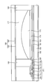
도 2는 도 1에 도시된 전기습윤 표시패널의 단위 화소들을 설명하는 평면도이다. 도 3은 도 2에 도시된 하나의 단위 화소를 절단선 I-I'으로 절단한 단면도이다.FIG. 2 is a plan view illustrating unit pixels of the electrowetting display panel illustrated in FIG. 1. 3 is a cross-sectional view of one unit pixel illustrated in FIG. 2 taken along a cutting line II ′.
도 2 및 도 3을 참조하면, 제1 투명 기판(105) 위에는 가로 방향의 스캔 라인(SL)과, 상기 스캔 라인(SL)에서 돌출된 게이트 전극(110)이 형성된다. 상기 제1 투명 기판(105)은 리지드 타입(Rigid type)일 수도 있고, 필름이나 플라스틱과 같은 플렉서블 타입(Flexible type)일 수도 있다. 상기 리지드 타입의 기판은 유리 기판, 석영 기판, 유리 세라믹 기판 및 결정 유리 기판을 포함한다. 상기 제1 투명 기판(105)에 채용되는 물질은 제조 공정시 높은 처리 온도에 대해 저항성(또는 내열성)을 갖는 것이 바람직하다. 2 and 3, a scan line SL in a horizontal direction and a
상기 스캔 라인(SL) 및 게이트 전극(110) 위에는 게이트 절연막(112)이 형성된다.A gate insulating layer 112 is formed on the scan line SL and the
상기 게이트 전극(110) 위에는 반도체층(114)과 불순물 반도체층(116)으로 이루어진 액티브층이 형성된다.An active layer including a
상기 게이트 절연막(112) 및 액티브층이 형성된 층 위에는 세로 방향의 데이터 라인(DL)과, 상기 데이터 라인(DL)에서 돌출되면서 상기 액티브층의 일부 영역을 커버하는 소스 전극(120)과, 상기 소스 전극(120)에서 일정 간격 이격되면서 상기 액티브층의 다른 일부 영역을 커버하는 드레인 전극(130)이 형성된다. 상기 게이트 전극(110), 반도체층(114), 불순물 반도체층(116), 소스 전극(120) 및 드레인 전극(130)은 박막 트랜지스터(TFT)를 정의한다.A data line DL in a vertical direction, a
상기 박막 트랜지스터(TFT)와 게이트 절연막(112) 위에는 패시베이션층(140)이 형성된다. 상기 패시베이션층(140)의 일부는 개구되어 상기 박막 트랜지스터(TFT)의 드레인 전극을 노출시킨다.The
ITO와 같은 도전성 산화물로 이루어지는 화소전극(150)은 상기 패시베이션층(140)을 개구시키는 콘택홀(CNT)을 경유하여 하부에 구비되는 박막 트랜지스터(TFT)의 드레인 전극(130)과 전기적으로 연결된다.The
상기 화소전극(150)의 가장 자리 영역을 둘러싸면서 일정 높이의 격벽(Bank)(160)이 형성된다. 상기 격벽(160)의 정점부들은 동일한 평면에 배치되도록 균일한 것이 바람직하다. A
일례로, 상기 격벽(160)은 단위 화소 영역을 둘러싸는 폐루프 형상을 갖는다. 다른 일례로, 상기 격벽(160)은 단위 화소 영역을 둘러싸면서 인접하는 단위 화소 영역을 둘러싸는 격벽과 서로 연결된 형상을 갖는다. 이에 따라, 상기 격벽 (160)은 상기 단위 화소 영역을 둘러싸는 스캔 라인들과 데이터 라인들에 대응하여 오버레이된다. For example, the
상기 격벽(160)에 의해 정의되는 일정 공간의 바닥부에는 소수성 절연막(170)이 코팅된다. 상기 격벽(160)은 유기막 포토 공정에 의해 형성될 수도 있고, 인장 공정(또는 스탬프 공정)에 의해 형성될 수도 있다. 상기 소수성 절연막(170)은 스핀 코팅 방식에 의해 형성될 수도 있고, 잉크젯 분사 방식에 의해 형성될 수도 있다. The hydrophobic insulating
상기 소수성 절연막(170)을 바닥으로 하여 상기 격벽(160)에 의해 둘러 쌓이는 영역에는 소수성 액체(non-aqueous liquid)(175)와 친수성 액체(aqueous liquid)(177)의 혼합물인 도전성 착색 액체(또는 도전성 물방울)가 충진된다. 상기 소수성 액체는 컬러 오일이 바람직하다. 상기 컬러 오일은 레드 컬러 오일, 블루 컬러 오일, 그린 컬러 오일과 같이 다양한 컬러를 가질 수 있다.A conductive coloring liquid (or a mixture of a
상기 격벽(160)은 상기 도전성 착색 액체를 수용하는 역할과 함께 어레이 기판과 대향 기판(180)간의 셀갭을 유지시키는 스페이서의 역할도 수행한다. 상기 격벽(160)이 스페이서의 역할을 수용하므로 데이터 라인(DL)이나 스캔 라인(SL)간의 공간을 최대한 활용해 주기 위하여 박막 트랜지스터(TFT)를 제외한 영역부터 화소전극의 가장자리 영역까지 격벽을 형성하는 것이 바람직하다.The
상기 대향 기판(180)은 어레이 기판에 형성된 격벽(160)에 대향하도록 합체된다. 상기 대향 기판(180)은 투명 기판(182)과 상기 투명 기판(182) 위에 형성된 공통전극(184)을 포함한다. 상기 공통전극(184)은 외부에서 제공되는 공통전극전압 (Vcom)을 매 화소에 전달한다. The opposing
이에 따라, 단위 화소 영역에 채워진 도전성 착색 액체는 하기하는 도 4a 및 도 4b에 나타낸 바와 같이, 화소전극(150)에 인가되는 데이터 전압과 공통전극(184)에 인가되는 공통전극전압(Vcom)간의 전위차에 응답하여 흩어지거나 뭉쳐져 영상을 표시한다.Accordingly, the conductive colored liquid filled in the unit pixel region is formed between the data voltage applied to the
이상에서는 어레이 기판에 형성된 격벽을 통해 도전성 착색 액체를 포획(또는 격납)하는 전기습윤 표시패널을 일례로 설명하였으나, 상기 어레이 기판에 대향하는 대향 기판에 격벽을 형성하고, 형성된 격벽을 통해 도전성 착색 액체를 포획하는 전기습윤 표시패널에도 적용될 수 있음은 자명하다.In the above, the electrowetting display panel which captures (or stores) the conductive coloring liquid through the partition wall formed in the array substrate has been described as an example. However, the partition wall is formed on the counter substrate facing the array substrate, and the conductive coloring liquid is formed through the formed partition wall. It is obvious that the present invention can also be applied to an electrowetting display panel that captures a.
도 4a 및 도 4b는 본 발명에 따른 전기습윤 표시장치의 동작을 설명하는 개념도들이다. 특히, 도 4a 및 도 4b는 게이트 온 전압과 게이트 오프 전압의 인가에 따른 전기습윤 표시장치의 동작을 도시한다.4A and 4B are conceptual views illustrating the operation of the electrowetting display device according to the present invention. In particular, FIGS. 4A and 4B illustrate the operation of the electrowetting display device according to the application of the gate on voltage and the gate off voltage.
도 1 내지 도 3과 도 4a에 도시한 바와 같이, 박막 트랜지스터(TFT)가 턴-오프 상태를 유지하면, 상기 공통전극(184)에 일정 레벨의 공통전극전압(Vcom)이 인가되더라도 상기 화소전극(150)이 플로팅 상태를 유지하므로 상기 화소전극(150)과 공통전극(184)간에는 어떠한 전위차도 발생되지 않는다. 이에 따라, 상기 격벽(160)에 의해 정의되는 영역에 수용된 소수성 액체(175)는 전체적으로 퍼진 상태를 유지한다.As shown in FIGS. 1 to 3 and 4A, when the TFT is turned off, the pixel electrode may be applied even if a predetermined level of the common electrode voltage Vcom is applied to the
한편, 도 1 내지 도 3과 도 4b에 도시한 바와 같이, 박막 트랜지스터(TFT)가 턴-온되면, 상기 화소전극(150)에는 데이터 라인을 통해 전달되는 데이터 전압이 인가되고, 상기 공통전극(184)에는 상기 공통전극전압(Vcom)이 인가되므로 상기 화소전극(150)과 공통전극(184)간에는 일정 레벨의 전위치가 발생된다. 이에 따라, 격벽(160)에 의해 정의되는 영역에 수용된 소수성 액체(175)는 상기한 전위차에 대응하여 뭉쳐진 상태를 유지한다. 도 4b에서는 설명의 편의를 위해 상기 소수성 액체(175)가 상기 박막 트랜지스터(TFT)에 근접하도록 최소화된 표면적을 갖도록 뭉쳐진 상태를 도시하였으나, 이에 한정되는 것은 아니다.1 to 3 and 4B, when the thin film transistor TFT is turned on, a data voltage transferred through a data line is applied to the
도 5는 단위 화소들에 인가되는 데이터 전압에 따른 광반사율을 설명하는 단면도이다. 5 is a cross-sectional view illustrating light reflectance according to data voltages applied to unit pixels.
도 5를 참조하면, 좌측 화소 영역에는 레드 컬러의 도전성 착색 액체가 충진되고, 중앙 화소 영역에는 그린 컬러의 도전성 착색 액체가 충진되며, 우측 화소 영역에는 블루 컬러의 도전성 착색 액체가 충진된다. Referring to FIG. 5, a red colored conductive colored liquid is filled in the left pixel region, a green colored conductive colored liquid is filled in the central pixel region, and a blue colored conductive colored liquid is filled in the right pixel region.
상기 좌측 화소 영역의 화소전극(150)과 공통전극(182)간에는 무전계 상태 또는 낮은 레벨의 전위차가 발생된다. 상기 무전계 상태 또는 낮은 레벨의 전위차에 따라, 상기 레드 컬러의 도전성 착색 액체는 상기 좌측 화소 영역의 전체 영역에 걸쳐 퍼진 상태를 유지한다. 따라서, 외부의 입사광(LI)은 반사판(190)에 의해 반사되어 상기 좌측 화소 영역의 전체를 통해 레드광이 출사된다.An electric field or a low level potential difference is generated between the
한편, 상기 중앙 화소 영역의 화소전극(150)과 공통전극(182)간에는 중간 레벨의 전위차가 발생된다. 상기 중간 레벨의 전위차에 따라, 상기 그린 컬러의 도전성 착색 액체는 상기 중앙 화소 영역의 2/3 영역에 걸쳐 퍼진 상태를 유지하고, 나머지인 1/3 영역에서는 하부막을 노출시키는 상태를 유지한다. 따라서, 외부의 입 사광(LI)은 반사판(190)에 의해 반사되어 상기 2/3 영역을 통해 그린광이 출사되고, 상기 1/3 영역을 통해 화이트광이 출사된다.Meanwhile, an intermediate level potential difference is generated between the
다른 한편, 상기 우측 화소 영역의 화소전극(150)과 공통전극(182)간에는 높은 레벨의 전위차가 발생된다. 상기 높은 레벨의 전위차에 따라, 상기 블루 컬러의 도전성 착색 액체는 상기 우측 화소 영역의 1/3 영역에 걸쳐 퍼진 상태를 유지하고, 나머지인 2/3 영역에서는 하부막을 노출시키는 상태를 유지한다. 따라서, 외부의 입사광(LI)은 반사판(190)에 의해 반사되어 상기 1/3 영역을 통해 블루광이 출사되고, 상기 2/3 영역을 통해 화이트광이 출사된다.On the other hand, a high level potential difference is generated between the
이상에서 설명한 방식을 통해 화소전극과 공통전극간에 인가되는 전위차에 응답하여 도전성 착색 액체의 표면적이 변경되고, 표면적이 변경된 도전성 착색 액체에 따라 반사되는 광량이 조절되어 다양한 계조 레벨을 갖는 영상을 표시한다.The surface area of the conductive coloring liquid is changed in response to the potential difference applied between the pixel electrode and the common electrode through the method described above, and the amount of reflected light is adjusted according to the conductive coloring liquid whose surface area is changed to display an image having various gradation levels. .
<전기습윤 표시패널의 제조 방법-1><Method of manufacturing electrowetting display panel-1>
도 6a 내지 도 6f는 본 발명의 제1 실시예에 따른 전기습윤 표시패널의 제조 공정을 설명하는 공정도들이다. 특히, 도 6a 내지 도 6f는 포토 공정에 의해 제조되는 전기습윤 표시패널의 제조 공정을 도시한다.6A through 6F are process diagrams illustrating a manufacturing process of an electrowetting display panel according to a first exemplary embodiment of the present invention. In particular, FIGS. 6A to 6F illustrate a manufacturing process of an electrowetting display panel manufactured by a photo process.
도 6a를 참조하면, 유리나 세라믹 등의 절연 물질로 이루어진 제1 투명 기판(105) 위에 탄탈륨(Ta), 티타늄(Ti), 몰리브덴(Mo), 알루미늄(Al), 크롬(Cr), 구리(Cu) 또는 텅스텐(W) 등과 같은 금속을 증착한다. 이어, 증착된 금속을 패터닝하여 가로 방향으로 신장되고 세로 방향으로 배열되는 복수의 스캔 라인들과, 상기 스캔 라인으로부터 연장된 게이트 전극(110)을 형성한다. 이어, 상기 게이트 전극(110) 을 포함하는 기판의 전면에 질화 실리콘 등을 플라즈마 화학 기상 증착법으로 적층하여 게이트 절연층(112)을 형성한다. 상기 게이트 절연층(112)은 상기 제1 투명 기판(105)의 전면에 형성될 수도 있고, 상기 스캔 라인과 게이트 전극(110)을 커버하도록 패터닝될 수도 있다. Referring to FIG. 6A, tantalum (Ta), titanium (Ti), molybdenum (Mo), aluminum (Al), chromium (Cr), and copper (Cu) are formed on a first
이어, 상기 게이트 절연층(112) 위에 아몰퍼스-실리콘(a-Si) 막 및 인 시튜(insitu) 도핑된 n+ 아몰퍼스 실리콘(a-Si) 막을 형성하고, 박막 트랜지스터를 정의하기 위해 일부 영역을 패터닝하여 상기 게이트 전극(110)이 위치한 영역에 반도체층(114)과 불순물 반도체층(116)을 형성한다. Subsequently, an amorphous-silicon (a-Si) film and an insitu doped n + amorphous silicon (a-Si) film are formed on the gate insulating layer 112, and some regions are patterned to define a thin film transistor. The
이어, 탄탈륨(Ta), 티타늄(Ti), 몰리브덴(Mo), 알루미늄(Al), 크롬(Cr), 구리(Cu) 또는 텅스텐(W) 등과 같은 금속을 증착한다. 이어, 상기 증착된 금속을 패터닝하여 복수의 데이터 라인들과, 상기 데이터 라인에서 연장된 소스 전극(120)과, 상기 소스 전극(120)과 일정 간격 이격된 드레인 전극(130)을 형성한다. Subsequently, metals such as tantalum (Ta), titanium (Ti), molybdenum (Mo), aluminum (Al), chromium (Cr), copper (Cu), or tungsten (W) are deposited. Subsequently, the deposited metal is patterned to form a plurality of data lines, a
이어, 스핀 코팅 방법으로 레지스트를 적층하여 패시베이션층(140)을 형성하고, 상기 패시베이션층(140)의 일부를 개구하여 상기 드레인 전극(130)을 노출시킨다. 이어, 결과물 상에 단위 화소 영역내에서 상기 드레인 전극(130)과 전기적으로 연결되는 화소전극(150)을 형성한다. 상기 화소전극(150)은 투명한 도전성 물질로 형성될 수 있다. 이러한 투명한 도전성 물질의 예로서는 산화 주석 인듐(Indium Tin Oxide, ITO), 산화 아연 인듐(Indium Zinc Oxide, IZO), 산화 아연(Zinc Oxide, ZO) 등을 들 수 있다. 이때, 상기 화소전극(150)은 전면 도포후 상기 단위 화소 영역에 대응하는 화소전극만 남겨지도록 패터닝될 수도 있고, 상기 단위 화소 영역에만 형성되도록 부분적으로 도포될 수도 있다. Subsequently, the
도 6b를 참조하면, 상기 도 6a에 의한 결과물 상에 일정 두께의 제1 유기절연막(159)을 후박하게 형성한다. 상기 제1 유기절연막(159)의 높이는 셀갭에 대응하는 것이 바람직하다.Referring to FIG. 6B, the first organic insulating
도 6c를 참조하면, 상기 도 6b에 의한 결과물 위에 단위 화소 영역을 정의하기 위해 상기 단위 화소 영역에 대응하는 불투명 부재를 갖는 포토 마스크(MA)를 제1 유기절연막(159) 상에 위치시킨다. 이어, 노광 공정, 현상 공정, 에칭 공정 및 박리 공정을 수행하여, 상기 수용 공간에 대응하는 제1 유기절연막(159)은 제거하므로써 도전성 착색 액체를 가두기 위한 격벽(160)을 형성한다. 상기 격벽(160)은 친수성 액체와 소수성 액체인 컬러 오일의 혼합물인 도전성 착색 액체를 포획하는 역할과 함께, 어레이 기판과 대향 기판간의 셀갭을 유지시켜주는 스페이서로서의 역할을 수행한다. 따라서, 단위 화소 영역을 제외한 영역 또는 단위 화소 영역과 박막 트랜지스터가 형성된 영역을 제외한 나머지 영역에 격벽을 형성하는 것이 바람직하다.Referring to FIG. 6C, a photo mask MA having an opaque member corresponding to the unit pixel region is positioned on the first organic insulating
도 6d를 참조하면, 상기 격벽(160)에 의해 정의되는 수용 공간에 제1 탱커(TNK1)에 충진된 소수성 액체를 잉크젯 분사 방식으로 분사하여 소수성 절연막(170)을 형성한다. 물론, 상기 소수성 절연막(170)은 스핀 코팅 방식에 의해 형성될 수도 있다. Referring to FIG. 6D, the hydrophobic insulating
도 6e를 참조하면, 상기 소수성 절연막(170)을 바닥으로 하여 상기 격벽(160)에 의해 둘러싸이는 공간에 제2 탱커(TNK2)에 충진된 소수성 액체를 잉크젯 분사 방식으로 분사하여 소수성 액체(non-aqueous liquid)(175)를 일정 체적만큼 형성한다. 상기 소수성 액체는 컬러 오일이 바람직하다. 상기 컬러 오일은 레드 컬러 오일, 블루 컬러 오일, 그린 컬러 오일과 같이 다양한 컬러를 가질 수 있다.Referring to FIG. 6E, the hydrophobic liquid filled in the second tanker TNK2 is injected into the space surrounded by the
도 6f를 참조하면, 상기 도 6e에 의해 형성된 소수성 액체가 건조되기 이전에 제3 탱커(TNK3)에 충진된 친수성 액체를 잉크젯 분사 방식으로 분사하여 친수성 액체(aqueous liquid)(177)를 가득 채운다. 이어, 도 3에 도시된 바와 같이, 제2 투명 기판(182)에 형성된 공통전극(184)이 친수성 액체(177)에 접하도록 배치시켜 격벽에 의해 정의되는 공간에 충진된 도전성 착색 액체를 밀봉하여 전기습윤 표시패널을 완성한다.Referring to FIG. 6F, the hydrophilic liquid filled in the third tanker TNK3 is sprayed by an inkjet injection method before the hydrophobic liquid formed by FIG. 6E is dried to fill the
<전기습윤 표시패널의 제조 방법-2><Method for Manufacturing Electro-Wet Display Panel-2>
도 7a 내지 도 7g는 본 발명의 제2 실시예에 따른 전기습윤 표시패널의 제조 공정을 설명하는 공정도들이다. 특히, 도 7a 내지 도 7g는 인장(imprint) 공정(또는 스탬프 공정)에 의해 제조되는 전기습윤 표시패널의 제조 공정을 도시한다.7A to 7G are process diagrams illustrating a manufacturing process of an electrowetting display panel according to a second exemplary embodiment of the present invention. In particular, FIGS. 7A to 7G illustrate a manufacturing process of an electrowetting display panel manufactured by an imprint process (or a stamp process).
도 7a는 상기한 도 6a에서 설명한 공정과 동일하므로 동일한 도면 번호를 부여하고 그 설명은 생략한다.Since FIG. 7A is the same as the process described with reference to FIG. 6A, the same reference numerals are given and the description thereof is omitted.
도 7b를 참조하면, 상기 도 7a에 의한 결과물 상에 일정 두께의 제2 유기절연막(259)을 후박하게 형성한다. 상기 제2 유기절연막(259)의 높이는 향후 인장 공정에 의해 격벽이 형성되는 점을 감안할 때 상기 도 6b에서 형성한 제1 유기절연막(159)의 높이보다는 낮다. Referring to FIG. 7B, a second organic insulating
도 7c 및 도 7d를 참조하면, 상기 도 7b에 의한 결과물 위에 단위 화소 영역 을 정의하기 위해 상기 단위 화소 영역에 대응하는 돌출부재를 갖는 스탬퍼(STM)를 유기절연막(259) 상에 위치시키고, 소정의 힘으로 가압한다. 상기 돌출부재는 화소전극의 가장 자리 영역을 폐루프 형상으로 둘러싸는 형상을 갖는다. 이에 따라, 상기 돌출부재에 대응하는 제2 유기절연막(259)은 상기 돌출부재가 미형성된 영역으로 이동되어 도전성 착색 액체를 가두기 위한 격벽(260)을 정의한다. 7C and 7D, a stamper STM having a protrusion member corresponding to the unit pixel region is positioned on the organic insulating
상기 도 7d에서는 인장 공정 완료후 일정 두께의 유기절연막이 잔류한 것을 도시하였으나, 상기 격벽을 제외한 나머지 영역에 대응하는 제2 유기절연막(259)을 완전 제거할 수도 있다.Although FIG. 7D illustrates that the organic insulating film having a predetermined thickness remains after the stretching process is completed, the second organic insulating
도 7e를 참조하면, 상기 격벽(260)에 의해 정의되는 수용 공간에 제1 탱커(TNK1)에 충진된 소수성 액체를 잉크젯 분사 방식으로 분사하여 소수성 절연막(270)을 형성한다. 물론, 상기 소수성 절연막(270)은 스핀 코팅 방식에 의해 형성될 수도 있다. Referring to FIG. 7E, a hydrophobic insulating
도 7f를 참조하면, 상기 소수성 절연막(270)을 바닥으로 하여 상기 격벽(260)에 의해 둘러싸이는 공간에 제2 탱커(TNK2)에 충진된 소수성 액체를 잉크젯 분사 방식으로 분사하여 소수성 액체(non-aqueous liquid)(275)를 일정 체적만큼 형성한다. 상기 소수성 액체는 컬러 오일이 바람직하다. 상기 컬러 오일은 레드 컬러 오일, 블루 컬러 오일, 그린 컬러 오일과 같이 다양한 컬러를 가질 수 있다.Referring to FIG. 7F, the hydrophobic liquid filled in the second tanker TNK2 is injected into the space surrounded by the
도 7g를 참조하면, 상기 도 7f에 의해 형성된 소수성 액체가 건조되기 이전에 제3 탱커(TNK3)에 충진된 친수성 액체를 잉크젯 분사 방식으로 분사하여 친수성 액체(aqueous liquid)(277)를 가득 채운다. 이어, 제2 투명 기판(182)에 형성된 공 통전극(184)이 친수성 액체(277)에 접하도록 배치시켜 격벽에 의해 정의되는 공간에 충진된 도전성 착색 액체를 밀봉하여 전기습윤 표시패널을 완성한다.Referring to FIG. 7G, a hydrophilic liquid filled in the third tanker TNK3 is sprayed by an inkjet injection method before the hydrophobic liquid formed by FIG. 7F is dried, thereby filling the
이상에서 설명한 바와 같이, 박막 트랜지스터와 화소전극이 형성된 어레이 기판 위에 전기습윤에 사용될 액체들을 포획하기 위한 격벽(Bank)을 형성한다. 상기한 격벽은 유기막 포토 공정을 이용하여 형성될 수도 있고, 인장 공정을 이용하여 형성될 수도 있다. 이어, 격벽에 의해 정의되는 일정 수납 공간의 바닥부에 소수성 절연막을 스핀 코팅 또는 잉크젯 분사 방식으로 코팅하고, 전기습윤에 사용되는 액체, 즉 컬러 오일 및 친수성 액체를 잉크젯 분사 방식으로 순차적으로 분사한 후 공통전극이 형성된 대향 기판으로 밀봉한다.As described above, a barrier for capturing liquids to be used for electrowetting is formed on the array substrate on which the thin film transistor and the pixel electrode are formed. The partition wall may be formed using an organic film photo process or may be formed using a tensile process. Subsequently, a hydrophobic insulating film is coated on the bottom of a predetermined storage space defined by the partition wall by spin coating or ink jet spraying, and the liquids used for electrowetting, that is, color oil and hydrophilic liquid are sequentially sprayed by ink jet spraying. It is sealed by the opposite substrate on which the common electrode is formed.
이에 따라, 전기습윤 표시패널의 하부 기판으로 액티브 매트릭스 타입의 어레이 기판이 이용되므로 별도의 제조 라인을 구축하는데 소요되는 비용이나 시간, 인력 등을 절감하면서 전기습윤 표시패널을 제조할 수 있다.Accordingly, since the active matrix type array substrate is used as the lower substrate of the electrowetting display panel, the electrowetting display panel can be manufactured while reducing the cost, time, and manpower required to construct a separate manufacturing line.
이상에서는 실시예를 참조하여 설명하였지만, 해당 기술 분야의 숙련된 당업자는 하기의 특허 청구의 범위에 기재된 본 발명의 사상 및 영역으로부터 벗어나지 않는 범위 내에서 본 발명을 다양하게 수정 및 변경시킬 수 있음을 이해할 수 있을 것이다.Although described above with reference to the embodiments, those skilled in the art can be variously modified and changed within the scope of the invention without departing from the spirit and scope of the invention described in the claims below. I can understand.
Claims (20)
Priority Applications (5)
| Application Number | Priority Date | Filing Date | Title |
|---|---|---|---|
| KR1020050051522A KR101129435B1 (en) | 2005-06-15 | 2005-06-15 | Electrowetting display panel and manufacturing method thereof |
| JP2006154183A JP5546713B2 (en) | 2005-06-15 | 2006-06-02 | Electric wet display panel and manufacturing method thereof |
| CN2006100936534A CN1881003B (en) | 2005-06-15 | 2006-06-14 | Electrowetting display panel and method for manufacturing same |
| US11/453,643 US7852547B2 (en) | 2005-06-15 | 2006-06-14 | Electro-wetting display panel and method of manufacturing the same |
| TW095121342A TWI395038B (en) | 2005-06-15 | 2006-06-15 | Electro-wetting display panel and method of manufacturing the same |
Applications Claiming Priority (1)
| Application Number | Priority Date | Filing Date | Title |
|---|---|---|---|
| KR1020050051522A KR101129435B1 (en) | 2005-06-15 | 2005-06-15 | Electrowetting display panel and manufacturing method thereof |
Publications (2)
| Publication Number | Publication Date |
|---|---|
| KR20060131240A KR20060131240A (en) | 2006-12-20 |
| KR101129435B1 true KR101129435B1 (en) | 2012-03-27 |
Family
ID=37519259
Family Applications (1)
| Application Number | Title | Priority Date | Filing Date |
|---|---|---|---|
| KR1020050051522A Expired - Fee Related KR101129435B1 (en) | 2005-06-15 | 2005-06-15 | Electrowetting display panel and manufacturing method thereof |
Country Status (5)
| Country | Link |
|---|---|
| US (1) | US7852547B2 (en) |
| JP (1) | JP5546713B2 (en) |
| KR (1) | KR101129435B1 (en) |
| CN (1) | CN1881003B (en) |
| TW (1) | TWI395038B (en) |
Families Citing this family (96)
| Publication number | Priority date | Publication date | Assignee | Title |
|---|---|---|---|---|
| JP4967290B2 (en) * | 2005-09-22 | 2012-07-04 | ソニー株式会社 | Optical element |
| TWI363920B (en) | 2007-05-25 | 2012-05-11 | Ind Tech Res Inst | Electrical field controlled surface tension displace devices and fabrication methods thereof |
| CN101681580B (en) * | 2007-06-19 | 2012-09-19 | 夏普株式会社 | Display element and electronic device using same |
| CN101355838B (en) * | 2007-07-25 | 2010-12-29 | 群康科技(深圳)有限公司 | Electric moistening display |
| CN101359091B (en) * | 2007-08-03 | 2010-09-29 | 群康科技(深圳)有限公司 | Electrowetting display and manufacturing method thereof |
| TWI385413B (en) * | 2007-08-10 | 2013-02-11 | Chimei Innolux Corp | Electro-wetting display and fabricating method thereof |
| CN101378611B (en) * | 2007-08-31 | 2011-12-07 | 群康科技(深圳)有限公司 | Active electric moisten display |
| US8111465B2 (en) * | 2007-09-12 | 2012-02-07 | University Of Cincinnati | Electrofluidic devices, visual displays, and methods for making and operating such electrofluidic devices |
| CN101393320B (en) * | 2007-09-21 | 2010-08-25 | 群康科技(深圳)有限公司 | Electric moisten display device |
| CN101398532B (en) * | 2007-09-28 | 2010-09-29 | 群康科技(深圳)有限公司 | Electrowetting display |
| GB0720484D0 (en) * | 2007-10-19 | 2007-11-28 | Seereal Technologies Sa | Cells |
| CN101424783B (en) * | 2007-11-02 | 2010-09-29 | 群康科技(深圳)有限公司 | Electrowetting display |
| CN101430421B (en) * | 2007-11-07 | 2010-09-29 | 群康科技(深圳)有限公司 | Electrowetting display |
| GB0722812D0 (en) * | 2007-11-21 | 2008-01-02 | Liquavista Bv | Method of making an electrowetting device, apparatus for carrying out the method and electrowetting device |
| GB0723861D0 (en) * | 2007-12-06 | 2008-01-23 | Liquavista Bv | Transflective electrowetting display device |
| JP2009211047A (en) * | 2008-02-05 | 2009-09-17 | Sony Corp | Liquid optical element |
| CN101593756B (en) * | 2008-05-28 | 2011-05-18 | 群康科技(深圳)有限公司 | Thin film transistor (TFT) substrate, manufacturing method thereof and display device |
| TWI393917B (en) * | 2008-06-06 | 2013-04-21 | Ind Tech Res Inst | Electrowetting display and method of manufacturing same |
| GB0811811D0 (en) * | 2008-06-27 | 2008-07-30 | Liquavista Bv | Electrowetting display device |
| TWI380254B (en) * | 2008-08-08 | 2012-12-21 | Prime View Int Co Ltd | Flexible display panel and fabricating method thereof |
| TWI418848B (en) * | 2008-08-29 | 2013-12-11 | Prime View Int Co Ltd | Pixel structure for use in a display and display using the same |
| US20150357480A1 (en) * | 2008-09-08 | 2015-12-10 | Gang Yu | Stable metal-oxide thin film transistor and method of making |
| TW201018956A (en) * | 2008-11-05 | 2010-05-16 | Ind Tech Res Inst | Method for fabricating electrowetting displays |
| TWI395974B (en) * | 2008-11-21 | 2013-05-11 | Ind Tech Res Inst | Color electrowetting display (ewd) devices |
| CN101750732B (en) * | 2008-12-08 | 2012-07-11 | 财团法人工业技术研究院 | Color electrowetting display device |
| US8717664B2 (en) | 2012-10-02 | 2014-05-06 | Sipix Imaging, Inc. | Color display device |
| US8964282B2 (en) | 2012-10-02 | 2015-02-24 | E Ink California, Llc | Color display device |
| JP5526607B2 (en) * | 2009-05-29 | 2014-06-18 | 株式会社リコー | Display element |
| TWI407146B (en) | 2009-06-10 | 2013-09-01 | Ind Tech Res Inst | Electrowetting display and method for fabricating the same |
| US9180454B2 (en) * | 2009-08-14 | 2015-11-10 | University Of Cincinnati | Electrowetting and electrofluidic devices with laplace barriers and related methods |
| GB0922690D0 (en) * | 2009-12-30 | 2010-02-17 | Liquavista Bv | Electrowetting display device |
| TWI418849B (en) * | 2009-12-31 | 2013-12-11 | Wintek Corp | Electrowetting display and pixel array substrate thereof and electrowetting display pixel structure thereof |
| US8729551B2 (en) * | 2010-03-17 | 2014-05-20 | Samsung Display Co., Ltd. | Flat panel display |
| DE102010013151B4 (en) * | 2010-03-27 | 2012-06-21 | Advanced Display Technology Ag | Display device with display elements without return channels |
| US8704756B2 (en) | 2010-05-26 | 2014-04-22 | Sipix Imaging, Inc. | Color display architecture and driving methods |
| US9116412B2 (en) | 2010-05-26 | 2015-08-25 | E Ink California, Llc | Color display architecture and driving methods |
| CN101852916B (en) * | 2010-06-01 | 2013-01-02 | 高婧 | Adjustable optical switch |
| US8723759B2 (en) * | 2010-06-23 | 2014-05-13 | Sharp Kabushiki Kaisha | Display with light concentrating substrate |
| JP5716032B2 (en) * | 2010-09-22 | 2015-05-13 | 積水化学工業株式会社 | Electrowetting display |
| KR20120043422A (en) | 2010-10-26 | 2012-05-04 | 삼성전자주식회사 | Electrowetting display device |
| TW201226972A (en) * | 2010-12-29 | 2012-07-01 | Ind Tech Res Inst | Electrofluidic device and driving method thereof |
| GB201104713D0 (en) * | 2011-03-21 | 2011-05-04 | Liquavista Bv | Dispensing method and device for dispensing |
| US8786935B2 (en) | 2011-06-02 | 2014-07-22 | Sipix Imaging, Inc. | Color electrophoretic display |
| US9013783B2 (en) | 2011-06-02 | 2015-04-21 | E Ink California, Llc | Color electrophoretic display |
| KR101852429B1 (en) * | 2011-06-16 | 2018-04-26 | 엘지전자 주식회사 | Liquid micro shutter display device |
| US8605354B2 (en) | 2011-09-02 | 2013-12-10 | Sipix Imaging, Inc. | Color display devices |
| US8649084B2 (en) | 2011-09-02 | 2014-02-11 | Sipix Imaging, Inc. | Color display devices |
| GB201116093D0 (en) | 2011-09-16 | 2011-11-02 | Samsung Lcd Nl R & D Ct Bv | Display device |
| TWI581005B (en) * | 2011-10-24 | 2017-05-01 | 積水化學工業股份有限公司 | Method for producing electrowetting elements, and electrowetting display |
| KR101912340B1 (en) * | 2011-11-15 | 2018-10-29 | 엘지디스플레이 주식회사 | Apparatus for oil dosing and method of fabricating electrowetting display device using the same |
| GB201120777D0 (en) * | 2011-12-02 | 2012-01-11 | Samsung Lcd Nl R & D Ct Bv | Electrowetting display device |
| US20140355100A1 (en) * | 2012-01-18 | 2014-12-04 | Sharp Kabushiki Kaisha | Display element and electrical device using the same |
| US8982444B2 (en) | 2012-02-09 | 2015-03-17 | Amazon Technologies, Inc. | Electrowetting display device and manufacturing method thereof |
| KR101931542B1 (en) * | 2012-02-09 | 2019-03-20 | 리쿠아비스타 비.브이. | Electrowetting display device and manufacturing method thereof |
| US8917439B2 (en) | 2012-02-09 | 2014-12-23 | E Ink California, Llc | Shutter mode for color display devices |
| KR101963902B1 (en) * | 2012-08-08 | 2019-03-29 | 리쿠아비스타 비.브이. | Electrowetting display device and manufacturing method thereof |
| KR101896703B1 (en) * | 2012-02-17 | 2018-10-04 | 리쿠아비스타 비.브이. | Electrowetting display device and manufacturing method thereof |
| KR101379010B1 (en) * | 2012-03-23 | 2014-03-27 | 한국과학기술원 | Electrowetting varifocal lens array having vertical electrode structure and method for fabrication the same |
| KR101933718B1 (en) | 2012-03-27 | 2018-12-28 | 리쿠아비스타 비.브이. | Electro wetting display device |
| KR101408784B1 (en) * | 2012-03-30 | 2014-06-18 | 세메스 주식회사 | Substrate treating apparatus and substrate treating method |
| JP5919967B2 (en) * | 2012-04-02 | 2016-05-18 | セイコーエプソン株式会社 | Electrophoretic display device and electronic apparatus |
| KR101931373B1 (en) * | 2012-04-17 | 2018-12-20 | 리쿠아비스타 비.브이. | Substrate for an electro wetting display device and method of manufacturing the substrate |
| KR101941712B1 (en) * | 2012-06-05 | 2019-01-24 | 리쿠아비스타 비.브이. | Electrowetting display device and fabrication method of the same |
| GB201210345D0 (en) | 2012-06-12 | 2012-07-25 | Samsung Lcd Nl R & D Ct Bv | Electrowetting device |
| DE102012013725B4 (en) | 2012-07-11 | 2016-08-04 | Advanced Display Technology Ag | Electrically controllable display element for an optical display device and corresponding manufacturing method |
| US8797636B2 (en) | 2012-07-17 | 2014-08-05 | Sipix Imaging, Inc. | Light-enhancing structure for electrophoretic display |
| US9927623B2 (en) | 2012-07-18 | 2018-03-27 | Koninklijke Philips N.V. | Autostereoscopic lenticular display device |
| US9360733B2 (en) | 2012-10-02 | 2016-06-07 | E Ink California, Llc | Color display device |
| US11017705B2 (en) | 2012-10-02 | 2021-05-25 | E Ink California, Llc | Color display device including multiple pixels for driving three-particle electrophoretic media |
| CN102998791B (en) * | 2012-12-03 | 2015-04-01 | 京东方科技集团股份有限公司 | Electrowetting display device |
| CN105264434B (en) | 2013-04-18 | 2018-09-21 | 伊英克加利福尼亚有限责任公司 | color display device |
| US9383623B2 (en) | 2013-05-17 | 2016-07-05 | E Ink California, Llc | Color display device |
| TWI514063B (en) | 2013-05-17 | 2015-12-21 | Sipix Imaging Inc | Color display device |
| EP2997420B1 (en) | 2013-05-17 | 2018-06-06 | E Ink California, LLC | Color display device with color filters |
| TWI485428B (en) | 2013-05-28 | 2015-05-21 | Ind Tech Res Inst | Electrowetting display panel |
| KR102078340B1 (en) * | 2013-07-17 | 2020-02-18 | 삼성디스플레이 주식회사 | Electro static discharge protection circuit and electronic device having the same |
| TWI534520B (en) | 2013-10-11 | 2016-05-21 | 電子墨水加利福尼亞有限責任公司 | Color display device |
| EP2868970B1 (en) | 2013-10-29 | 2020-04-22 | Honeywell Technologies Sarl | Regulating device |
| EP3095007B1 (en) | 2014-01-14 | 2020-03-25 | E Ink California, LLC | Method of driving a color display layer |
| PT3210076T (en) | 2014-02-19 | 2021-10-20 | E Ink California Llc | Color display device |
| US20150268531A1 (en) | 2014-03-18 | 2015-09-24 | Sipix Imaging, Inc. | Color display device |
| US9297998B2 (en) * | 2014-03-28 | 2016-03-29 | Amazon Technologies, Inc. | Electrode of an electrowetting device |
| CN103955053B (en) * | 2014-05-04 | 2016-05-25 | 南京晶奥微光电技术有限公司 | A kind of method of preparing the wetting display unit of electricity by impression |
| US10380955B2 (en) | 2014-07-09 | 2019-08-13 | E Ink California, Llc | Color display device and driving methods therefor |
| US10891906B2 (en) | 2014-07-09 | 2021-01-12 | E Ink California, Llc | Color display device and driving methods therefor |
| US10147366B2 (en) | 2014-11-17 | 2018-12-04 | E Ink California, Llc | Methods for driving four particle electrophoretic display |
| CN106199948A (en) * | 2016-07-06 | 2016-12-07 | 京东方科技集团股份有限公司 | The moistening structure of a kind of electricity, display module and display device |
| CN106373532B (en) * | 2016-10-27 | 2019-01-11 | 合肥京东方显示技术有限公司 | A kind of array substrate, Electrowetting display panel and display device |
| CN106646927B (en) * | 2016-11-02 | 2020-03-06 | 京东方科技集团股份有限公司 | Display panel and display device |
| US10156714B1 (en) * | 2017-03-22 | 2018-12-18 | Amazon Technologies, Inc. | Electrowetting pixel with bottom electrode to reduce electromagnetic fringe fields |
| CN107507582B (en) * | 2017-10-18 | 2019-06-07 | 福州大学 | A method of adjustment electric moistening display drive waveforms |
| US11266832B2 (en) | 2017-11-14 | 2022-03-08 | E Ink California, Llc | Electrophoretic active delivery system including porous conductive electrode layer |
| JP7438346B2 (en) | 2019-11-27 | 2024-02-26 | イー インク コーポレイション | Benefit Agent Delivery System Comprising Microcells with Electroerodible Seal Layer |
| CN111487761A (en) * | 2020-05-14 | 2020-08-04 | Tcl华星光电技术有限公司 | Electrowetting display panel and manufacturing method thereof |
| CN115729010B (en) | 2021-08-25 | 2023-09-22 | 荣耀终端有限公司 | Display screens and terminal equipment |
| CN115166964A (en) * | 2022-06-29 | 2022-10-11 | 合肥京东方显示技术有限公司 | 3D display device and 3D display apparatus |
Citations (3)
| Publication number | Priority date | Publication date | Assignee | Title |
|---|---|---|---|---|
| JP2000111899A (en) * | 1998-09-30 | 2000-04-21 | Toshiba Corp | Reflective liquid crystal display device and method of manufacturing the same |
| KR20010098900A (en) * | 2000-04-27 | 2001-11-08 | 니시무로 타이죠 | A liquid crystal display device and method of manufacturing thereof |
| KR20040036645A (en) * | 2002-10-25 | 2004-04-30 | 세이코 엡슨 가부시키가이샤 | Apparatus for arranging spacers at fixed points, liquid crystal device, method of manufacturing liquid crystal device, and electronic apparatus |
Family Cites Families (11)
| Publication number | Priority date | Publication date | Assignee | Title |
|---|---|---|---|---|
| JP4006925B2 (en) * | 2000-05-30 | 2007-11-14 | セイコーエプソン株式会社 | Method for manufacturing electrophoretic display device |
| WO2003045556A2 (en) * | 2001-11-26 | 2003-06-05 | Keck Graduate Institute | Method, apparatus and article for microfluidic control via electrowetting, for chemical, biochemical and biological assays and the like |
| GB0129068D0 (en) * | 2001-12-05 | 2002-01-23 | Koninl Philips Electronics Nv | Display device |
| JP4515035B2 (en) * | 2002-03-14 | 2010-07-28 | 株式会社半導体エネルギー研究所 | Display device and manufacturing method thereof |
| JP2003330047A (en) * | 2002-05-10 | 2003-11-19 | Seiko Epson Corp | Electro-optical device, method of manufacturing the same, and electronic apparatus |
| US7359108B2 (en) * | 2003-01-27 | 2008-04-15 | Liquavista B.V. | Display device |
| WO2004077124A1 (en) * | 2003-02-26 | 2004-09-10 | Koninklijke Philips Electronics N.V. | A passive matrix display with bistable electro-wetting cells |
| JP4402358B2 (en) * | 2003-03-05 | 2010-01-20 | キヤノン株式会社 | Color image display panel and driving method thereof |
| EP1629315B1 (en) * | 2003-05-22 | 2017-09-06 | Amazon Europe Holding Technologies SCS | Display device |
| JP2005084216A (en) * | 2003-09-05 | 2005-03-31 | Sanyo Electric Co Ltd | Display device |
| EP1671304B1 (en) * | 2003-10-08 | 2008-08-20 | E Ink Corporation | Electro-wetting displays |
-
2005
- 2005-06-15 KR KR1020050051522A patent/KR101129435B1/en not_active Expired - Fee Related
-
2006
- 2006-06-02 JP JP2006154183A patent/JP5546713B2/en not_active Expired - Fee Related
- 2006-06-14 CN CN2006100936534A patent/CN1881003B/en not_active Expired - Fee Related
- 2006-06-14 US US11/453,643 patent/US7852547B2/en not_active Expired - Fee Related
- 2006-06-15 TW TW095121342A patent/TWI395038B/en not_active IP Right Cessation
Patent Citations (3)
| Publication number | Priority date | Publication date | Assignee | Title |
|---|---|---|---|---|
| JP2000111899A (en) * | 1998-09-30 | 2000-04-21 | Toshiba Corp | Reflective liquid crystal display device and method of manufacturing the same |
| KR20010098900A (en) * | 2000-04-27 | 2001-11-08 | 니시무로 타이죠 | A liquid crystal display device and method of manufacturing thereof |
| KR20040036645A (en) * | 2002-10-25 | 2004-04-30 | 세이코 엡슨 가부시키가이샤 | Apparatus for arranging spacers at fixed points, liquid crystal device, method of manufacturing liquid crystal device, and electronic apparatus |
Also Published As
| Publication number | Publication date |
|---|---|
| JP5546713B2 (en) | 2014-07-09 |
| KR20060131240A (en) | 2006-12-20 |
| TW200705070A (en) | 2007-02-01 |
| CN1881003B (en) | 2012-04-25 |
| CN1881003A (en) | 2006-12-20 |
| JP2006350328A (en) | 2006-12-28 |
| US7852547B2 (en) | 2010-12-14 |
| US20060285067A1 (en) | 2006-12-21 |
| TWI395038B (en) | 2013-05-01 |
Similar Documents
| Publication | Publication Date | Title |
|---|---|---|
| KR101129435B1 (en) | Electrowetting display panel and manufacturing method thereof | |
| TWI468832B (en) | Electrophoretic display device and method of fabricating the same | |
| US11778886B2 (en) | Display substrate and preparation method thereof, and display apparatus | |
| TWI461809B (en) | Electrophoretic display device and method of manufacturing same | |
| JP4909323B2 (en) | Active matrix substrate, display panel, display device, and method of manufacturing active matrix substrate | |
| US9459444B2 (en) | Electrowetting display device with light absorbing partition walls | |
| CN102084412B (en) | Active matrix substrate, display panel, display device, and active matrix substrate manufacturing method | |
| CN102156372B (en) | Electro phoretic display device and manufacture method thereof | |
| EP2169711A1 (en) | Semiconductor device, semiconductor device manufacturing method, display device and display device manufacturing method | |
| US7436578B2 (en) | Electrophoretic display and manufacturing method thereof | |
| KR20140015829A (en) | Electrophoresis display device and method for manufacturing the same | |
| KR20120003713A (en) | Electro Wetting Display Device | |
| KR20110071668A (en) | Electrophoretic display device and manufacturing method thereof | |
| KR20100076822A (en) | Electrophoretic display device and method for fabricating the same | |
| KR20110025723A (en) | Electrophoretic display device and manufacturing method thereof | |
| KR20090043950A (en) | Color electronic ink display device and manufacturing method thereof | |
| KR20140074775A (en) | Electrophoretic display device and method of fabricating thereof | |
| KR20250082051A (en) | Display panel and manufacturing method for the same | |
| KR20250027384A (en) | Display panel and manufactuinf method for the same | |
| KR20060017162A (en) | Manufacturing method of liquid crystal display device | |
| KR20100045876A (en) | Electrophoretic display device and method for fabricating the same | |
| KR20060083030A (en) | Manufacturing Method of Display Board |
Legal Events
| Date | Code | Title | Description |
|---|---|---|---|
| PA0109 | Patent application |
St.27 status event code: A-0-1-A10-A12-nap-PA0109 |
|
| PN2301 | Change of applicant |
St.27 status event code: A-3-3-R10-R13-asn-PN2301 St.27 status event code: A-3-3-R10-R11-asn-PN2301 |
|
| PN2301 | Change of applicant |
St.27 status event code: A-3-3-R10-R13-asn-PN2301 St.27 status event code: A-3-3-R10-R11-asn-PN2301 |
|
| PG1501 | Laying open of application |
St.27 status event code: A-1-1-Q10-Q12-nap-PG1501 |
|
| A201 | Request for examination | ||
| E13-X000 | Pre-grant limitation requested |
St.27 status event code: A-2-3-E10-E13-lim-X000 |
|
| P11-X000 | Amendment of application requested |
St.27 status event code: A-2-2-P10-P11-nap-X000 |
|
| P13-X000 | Application amended |
St.27 status event code: A-2-2-P10-P13-nap-X000 |
|
| PA0201 | Request for examination |
St.27 status event code: A-1-2-D10-D11-exm-PA0201 |
|
| E902 | Notification of reason for refusal | ||
| PE0902 | Notice of grounds for rejection |
St.27 status event code: A-1-2-D10-D21-exm-PE0902 |
|
| P11-X000 | Amendment of application requested |
St.27 status event code: A-2-2-P10-P11-nap-X000 |
|
| P13-X000 | Application amended |
St.27 status event code: A-2-2-P10-P13-nap-X000 |
|
| E701 | Decision to grant or registration of patent right | ||
| PE0701 | Decision of registration |
St.27 status event code: A-1-2-D10-D22-exm-PE0701 |
|
| GRNT | Written decision to grant | ||
| PR0701 | Registration of establishment |
St.27 status event code: A-2-4-F10-F11-exm-PR0701 |
|
| PR1002 | Payment of registration fee |
St.27 status event code: A-2-2-U10-U11-oth-PR1002 Fee payment year number: 1 |
|
| PG1601 | Publication of registration |
St.27 status event code: A-4-4-Q10-Q13-nap-PG1601 |
|
| R18-X000 | Changes to party contact information recorded |
St.27 status event code: A-5-5-R10-R18-oth-X000 |
|
| PN2301 | Change of applicant |
St.27 status event code: A-5-5-R10-R11-asn-PN2301 |
|
| PN2301 | Change of applicant |
St.27 status event code: A-5-5-R10-R11-asn-PN2301 |
|
| PN2301 | Change of applicant |
St.27 status event code: A-5-5-R10-R14-asn-PN2301 |
|
| FPAY | Annual fee payment |
Payment date: 20150227 Year of fee payment: 4 |
|
| PR1001 | Payment of annual fee |
St.27 status event code: A-4-4-U10-U11-oth-PR1001 Fee payment year number: 4 |
|
| R18-X000 | Changes to party contact information recorded |
St.27 status event code: A-5-5-R10-R18-oth-X000 |
|
| PR1001 | Payment of annual fee |
St.27 status event code: A-4-4-U10-U11-oth-PR1001 Fee payment year number: 5 |
|
| PR1001 | Payment of annual fee |
St.27 status event code: A-4-4-U10-U11-oth-PR1001 Fee payment year number: 6 |
|
| FPAY | Annual fee payment |
Payment date: 20180302 Year of fee payment: 7 |
|
| PR1001 | Payment of annual fee |
St.27 status event code: A-4-4-U10-U11-oth-PR1001 Fee payment year number: 7 |
|
| FPAY | Annual fee payment |
Payment date: 20190304 Year of fee payment: 8 |
|
| PR1001 | Payment of annual fee |
St.27 status event code: A-4-4-U10-U11-oth-PR1001 Fee payment year number: 8 |
|
| PC1903 | Unpaid annual fee |
St.27 status event code: A-4-4-U10-U13-oth-PC1903 Not in force date: 20200316 Payment event data comment text: Termination Category : DEFAULT_OF_REGISTRATION_FEE |
|
| PC1903 | Unpaid annual fee |
St.27 status event code: N-4-6-H10-H13-oth-PC1903 Ip right cessation event data comment text: Termination Category : DEFAULT_OF_REGISTRATION_FEE Not in force date: 20200316 |