KR101073147B1 - Touch screen panel integrated flat panel display and manufacturing method - Google Patents
Touch screen panel integrated flat panel display and manufacturing method Download PDFInfo
- Publication number
- KR101073147B1 KR101073147B1 KR1020100030923A KR20100030923A KR101073147B1 KR 101073147 B1 KR101073147 B1 KR 101073147B1 KR 1020100030923 A KR1020100030923 A KR 1020100030923A KR 20100030923 A KR20100030923 A KR 20100030923A KR 101073147 B1 KR101073147 B1 KR 101073147B1
- Authority
- KR
- South Korea
- Prior art keywords
- touch screen
- display area
- sensing
- screen panel
- patterns
- Prior art date
- Legal status (The legal status is an assumption and is not a legal conclusion. Google has not performed a legal analysis and makes no representation as to the accuracy of the status listed.)
- Active
Links
Images


Classifications
-
- G—PHYSICS
- G06—COMPUTING OR CALCULATING; COUNTING
- G06F—ELECTRIC DIGITAL DATA PROCESSING
- G06F3/00—Input arrangements for transferring data to be processed into a form capable of being handled by the computer; Output arrangements for transferring data from processing unit to output unit, e.g. interface arrangements
- G06F3/01—Input arrangements or combined input and output arrangements for interaction between user and computer
- G06F3/03—Arrangements for converting the position or the displacement of a member into a coded form
- G06F3/041—Digitisers, e.g. for touch screens or touch pads, characterised by the transducing means
- G06F3/044—Digitisers, e.g. for touch screens or touch pads, characterised by the transducing means by capacitive means
- G06F3/0446—Digitisers, e.g. for touch screens or touch pads, characterised by the transducing means by capacitive means using a grid-like structure of electrodes in at least two directions, e.g. using row and column electrodes
-
- G—PHYSICS
- G06—COMPUTING OR CALCULATING; COUNTING
- G06F—ELECTRIC DIGITAL DATA PROCESSING
- G06F3/00—Input arrangements for transferring data to be processed into a form capable of being handled by the computer; Output arrangements for transferring data from processing unit to output unit, e.g. interface arrangements
- G06F3/01—Input arrangements or combined input and output arrangements for interaction between user and computer
- G06F3/03—Arrangements for converting the position or the displacement of a member into a coded form
- G06F3/041—Digitisers, e.g. for touch screens or touch pads, characterised by the transducing means
- G06F3/044—Digitisers, e.g. for touch screens or touch pads, characterised by the transducing means by capacitive means
- G06F3/0443—Digitisers, e.g. for touch screens or touch pads, characterised by the transducing means by capacitive means using a single layer of sensing electrodes
-
- G—PHYSICS
- G02—OPTICS
- G02F—OPTICAL DEVICES OR ARRANGEMENTS FOR THE CONTROL OF LIGHT BY MODIFICATION OF THE OPTICAL PROPERTIES OF THE MEDIA OF THE ELEMENTS INVOLVED THEREIN; NON-LINEAR OPTICS; FREQUENCY-CHANGING OF LIGHT; OPTICAL LOGIC ELEMENTS; OPTICAL ANALOGUE/DIGITAL CONVERTERS
- G02F1/00—Devices or arrangements for the control of the intensity, colour, phase, polarisation or direction of light arriving from an independent light source, e.g. switching, gating or modulating; Non-linear optics
- G02F1/01—Devices or arrangements for the control of the intensity, colour, phase, polarisation or direction of light arriving from an independent light source, e.g. switching, gating or modulating; Non-linear optics for the control of the intensity, phase, polarisation or colour
- G02F1/13—Devices or arrangements for the control of the intensity, colour, phase, polarisation or direction of light arriving from an independent light source, e.g. switching, gating or modulating; Non-linear optics for the control of the intensity, phase, polarisation or colour based on liquid crystals, e.g. single liquid crystal display cells
- G02F1/133—Constructional arrangements; Operation of liquid crystal cells; Circuit arrangements
- G02F1/1333—Constructional arrangements; Manufacturing methods
- G02F1/13338—Input devices, e.g. touch panels
-
- G—PHYSICS
- G06—COMPUTING OR CALCULATING; COUNTING
- G06F—ELECTRIC DIGITAL DATA PROCESSING
- G06F2203/00—Indexing scheme relating to G06F3/00 - G06F3/048
- G06F2203/041—Indexing scheme relating to G06F3/041 - G06F3/045
- G06F2203/04103—Manufacturing, i.e. details related to manufacturing processes specially suited for touch sensitive devices
-
- G—PHYSICS
- G06—COMPUTING OR CALCULATING; COUNTING
- G06F—ELECTRIC DIGITAL DATA PROCESSING
- G06F2203/00—Indexing scheme relating to G06F3/00 - G06F3/048
- G06F2203/041—Indexing scheme relating to G06F3/041 - G06F3/045
- G06F2203/04111—Cross over in capacitive digitiser, i.e. details of structures for connecting electrodes of the sensing pattern where the connections cross each other, e.g. bridge structures comprising an insulating layer, or vias through substrate
Landscapes
- Engineering & Computer Science (AREA)
- General Engineering & Computer Science (AREA)
- Theoretical Computer Science (AREA)
- Physics & Mathematics (AREA)
- General Physics & Mathematics (AREA)
- Human Computer Interaction (AREA)
- Nonlinear Science (AREA)
- Chemical & Material Sciences (AREA)
- Crystallography & Structural Chemistry (AREA)
- Mathematical Physics (AREA)
- Optics & Photonics (AREA)
- Position Input By Displaying (AREA)
- Devices For Indicating Variable Information By Combining Individual Elements (AREA)
Abstract
본 발명은 터치 스크린 패널을 평판표시장치의 상부기판 상에 직접 형성하는 구조에 관한 것으로, 상기 터치 스크린 패널에 형성되는 절연막을 상기 평판표시장치의 상부기판 및 하부기판을 봉지하는 실링재의 고온 소성 공정에 적합한 안정적인 열특성을 갖는 스핀 온 글라스(Spin On Glass, SOG) 막으로 구현하는 터치 스크린 패널 일체형 평판표시장치 및 그 제조방법을 제공한다.The present invention relates to a structure in which a touch screen panel is directly formed on an upper substrate of a flat panel display, and an insulating film formed on the touch screen panel seals an upper substrate and a lower substrate of the flat panel display. Provided are a touch screen panel integrated flat panel display and a method of manufacturing the same, which are implemented using a spin on glass (SOG) film having stable thermal characteristics suitable for the present invention.
Description
본 발명은 평판표시장치에 관한 것으로, 특히 터치 스크린 패널 일체형 평판표시장치 및 그 제조방법에 관한 것이다.BACKGROUND OF THE
터치 스크린 패널은 영상표시장치 등의 화면에 나타난 지시 내용을 사람의 손 또는 물체로 선택하여 사용자의 명령을 입력할 수 있도록 한 입력장치이다. The touch screen panel is an input device that allows a user to input a command by selecting an instruction displayed on a screen of a video display device or the like as a human hand or an object.
이를 위해, 터치 스크린 패널은 영상표시장치의 전면(front face)에 구비되어 사람의 손 또는 물체에 직접 접촉된 접촉위치를 전기적 신호로 변환한다. 이에 따라, 접촉위치에서 선택된 지시 내용이 입력신호로 받아들여진다. To this end, the touch screen panel is provided on the front face of the image display device to convert a contact position in direct contact with a human hand or an object into an electrical signal. Accordingly, the instruction content selected at the contact position is received as an input signal.
이와 같은 터치 스크린 패널은 키보드 및 마우스와 같이 영상표시장치에 연결되어 동작하는 별도의 입력장치를 대체할 수 있기 때문에 그 이용범위가 점차 확장되고 있는 추세이다. Such a touch screen panel can be replaced with a separate input device connected to the image display device such as a keyboard and a mouse, and the use range thereof is gradually expanding.
터치 스크린 패널을 구현하는 방식으로는 저항막 방식, 광감지 방식 및 정전용량 방식 등이 알려져 있으며, 이 중 정전용량 방식의 터치 스크린 패널은, 사람의 손 또는 물체가 접촉될 때 도전성 감지패턴이 주변의 다른 감지패턴 또는 접지전극 등과 형성하는 정전용량의 변화를 감지함으로써, 접촉위치를 전기적 신호로 변환한다.As a method of implementing a touch screen panel, a resistive film method, a light sensing method, and a capacitive method are known. By detecting a change in capacitance formed in another sensing pattern or ground electrode, the contact position is converted into an electrical signal.
이와 같은 터치 스크린 패널은 일반적으로 액정표시장치, 유기전계 발광 표시장치와 같은 평판표시장치의 외면에 부착되어 구성되는데, 별도로 제작된 터치 스크린 패널과 평판표시장치를 서로 부착하여 사용할 경우 제품의 전체적인 두께를 증가시키고, 제조 원가를 상승시킨다는 문제점이 있다.
Such a touch screen panel is generally configured to be attached to an outer surface of a flat panel display such as a liquid crystal display or an organic light emitting display. There is a problem of increasing the manufacturing cost and increase.
본 발명은 터치 스크린 패널을 평판표시장치의 상부기판 상에 직접 형성하는 구조에 관한 것으로, 상기 터치 스크린 패널에 형성되는 절연막을 상기 평판표시장치의 상부기판 및 하부기판을 봉지하는 실링재의 고온 소성 공정에 적합한 안정적인 열특성을 갖는 스핀 온 글라스(Spin On Glass, SOG) 막으로 구현하는 터치 스크린 패널 일체형 평판표시장치 및 그 제조방법을 제공함에 목적이 있다.The present invention relates to a structure in which a touch screen panel is directly formed on an upper substrate of a flat panel display, and an insulating film formed on the touch screen panel seals an upper substrate and a lower substrate of the flat panel display. It is an object of the present invention to provide a touch screen panel integrated flat panel display device and a method of manufacturing the same, which are implemented as a spin on glass (SOG) film having stable thermal properties suitable for the present invention.
상기 목적을 달성하기 위하여 본 발명의 실시예에 의한 터치 스크린 패널 일체형 평판표시장치는, 표시영역과, 상기 표시영역 외곽에 형성된 비표시영역으로 각각 구획되는 상부기판 및 하부기판과; 상기 상부기판의 표시영역 상에 형성된 제 1 및 제 2감지패턴들과; 상기 제 2감지패턴들을 연결하는 연결패턴들과; 상기 연결패턴들 및 감지패턴 사이에 형성되는 제 1절연막 및 상기 감지패턴들 상에 형성되는 제 2절연막과; 상기 상부기판 및 하부기판의 비표시영역 사이에 형성되는 실링재가 포함되며, 상기 제 1 및 제 2절연막은 스핀 온 글라스(SOG) 물질로 구현됨을 특징으로 한다.In order to achieve the above object, a touch screen panel integrated flat panel display device includes: an upper substrate and a lower substrate respectively divided into a display area and a non-display area formed outside the display area; First and second sensing patterns formed on the display area of the upper substrate; Connection patterns connecting the second sensing patterns; A first insulating film formed between the connection patterns and the sensing pattern and a second insulating film formed on the sensing patterns; A sealing material is formed between the non-display area of the upper substrate and the lower substrate, wherein the first and second insulating layers are made of a spin on glass (SOG) material.
이 때, 상기 스핀 온 글라스 물질은 실록세인(siloxane)계 화합물, 실라젠(silozene)계 화합물 및 실리케이트(silicate)계 화합물, 실세스키옥세인(Silsesquioxane)계 화합물 중 하나 이상의 화합물을 포함하여 구현되며, 상기 제 1 및 제 2절연막은 두께가 0. 5um 내지 2um로 형성된다.In this case, the spin-on glass material is implemented by including one or more of a siloxane-based compound, a silazene-based compound, a silicate-based compound, a silicate-based compound, and a silsesquioxane-based compound. The first and second insulating layers have a thickness of 0.5 μm to 2 μm.
또한, 상기 제1 감지패턴들은, 제1 방향을 따라 X 좌표가 동일한 하나의 열에 배치된 제1 감지셀 및 인접한 상기 제1 감지셀을 연결하는 제1 연결라인으로 구성되며, 상기 제2 감지패턴들은, 제2 방향을 따라 Y 좌표가 동일한 하나의 행에 배치된 제2 감지셀들로 구성된다.The first sensing patterns may include a first sensing cell arranged in a column having the same X coordinate along a first direction, and a first connection line connecting the adjacent first sensing cells to the second sensing pattern. Are composed of second sensing cells arranged in one row with the same Y coordinate along the second direction.
또한, 상기 제1 및 제2 감지패턴들이 형성되는 영역의 가장자리에 배치되어 상기 하나의 열 또는 행 단위의 감지패턴들을 감지라인과 전기적으로 연결하는 다수의 금속패턴들이 더 포함된다.The metal pattern may further include a plurality of metal patterns disposed at an edge of an area where the first and second sensing patterns are formed to electrically connect the sensing patterns of one column or row to the sensing line.
또한, 상기 다수의 연결패턴들 및 금속패턴들은 동일한 레이어 상에 형성되며, 상기 제1 및 제2 감지패턴들을 구현하는 물질보다 낮은 저항값을 갖는 물질로 구현된다.In addition, the plurality of connection patterns and the metal patterns are formed on the same layer and are formed of a material having a lower resistance value than a material implementing the first and second sensing patterns.
또한, 상기 하부기판은 다수의 제 1 전극, 유기층 및 제 2 전극으로 구성되는 유기발광소자를 구비한 복수의 화소들이 형성된 표시영역 및 상기 표시영역의 외곽에 위치하여 상기 복수의 화소들을 구동하기 위해 구동 회로가 구비된 비표시영역을 포함하여 구성된다.In addition, the lower substrate may include a display area in which a plurality of pixels including an organic light emitting element including a plurality of first electrodes, an organic layer, and a second electrode are formed, and positioned outside the display area to drive the plurality of pixels. It comprises a non-display area provided with a drive circuit.
또한, 본 발명의 실시예에 의한 터치 스크린 패널 일체형 평판표시장치의 제조방법은, 표시영역과 비표시영역으로 구획되는 상부기판의 표시영역 상에 연결패턴들, 제 1절연막, 제 1, 2감지패턴들, 제 2절연막으로 구성되는 터치 스크린 패널이 형성되는 단계와; 상기 제 1, 2절연막에 대하여 저온의 소프트 베이킹 공정이 수행되는 단계와; 상기 상부기판의 하면에 하부기판이 위치하고, 상기 상부기판 및 하부기판의 비표시영역 사이에 실링재가 도포되는 단계와; 상기 실링재에 대한 고온의 소성 공정 및 상기 제 1, 2절연막에 대한 고온의 경화 공정이 동시에 수행되는 단계가 포함되며, 상기 제 1 및 제 2절연막은 스핀 온 글라스(SOG) 물질로 구현된다.In addition, the method of manufacturing a touch screen panel integrated flat panel display device according to an embodiment of the present invention may include connecting patterns, a first insulating layer, and a first and second sensing pattern on a display area of an upper substrate partitioned into a display area and a non-display area. Forming a touch screen panel composed of patterns and a second insulating film; Performing a low temperature soft baking process on the first and second insulating films; Placing a lower substrate on a lower surface of the upper substrate and applying a sealing material between the upper substrate and the non-display area of the lower substrate; A high temperature firing process for the sealing material and a high temperature curing process for the first and second insulating layers are simultaneously performed, and the first and second insulating layers are made of a spin on glass (SOG) material.
여기서, 상기 스핀 온 글라스 물질은 실록세인(siloxane)계 화합물, 실라젠(silozene)계 화합물 및 실리케이트(silicate)계 화합물, 실세스키옥세인(Silsesquioxane)계 화합물 중 하나 이상의 화합물을 포함한 고형분과 상기 고형분을 녹이는 용매가 혼합된 용액 상태로 코팅되어 형성된다.Here, the spin on glass material may include a solid content and the solid content including one or more compounds of a siloxane compound, a silozene compound, a silicate compound, and a silsesquioxane compound. It is formed by coating a solvent solution to dissolve the mixed solution.
또한, 상기 소프트 베이킹 공정은 150℃ 내지 250℃의 온도에서 수행되고, 상기 고온의 소정 공정 및 고온의 경화 공정은 400℃ 내지 500℃의 온도에서 수행된다.In addition, the soft baking process is carried out at a temperature of 150 ℃ to 250 ℃, the predetermined temperature and the high temperature curing process is carried out at a temperature of 400 ℃ to 500 ℃.
또한, 상기 실링재는 산화물 분말이 포함된 프릿에 유기물을 첨가하여 젤 상태의 페이스트로 구현되어 상기 비표시영역에 도포된다. In addition, the sealing material is formed as a gel paste by adding an organic material to the frit containing the oxide powder is applied to the non-display area.
이와 같은 본 발명에 의하면, 터치 스크린 패널을 평판표시장치의 상부기판 상에 직접 형성함에 있어, 터치 스크린 패널에 형성되는 절연막을 상기 평판표시장치의 상부기판 및 하부기판을 봉지하는 실링재의 고온 소성 공정에 적합한 안정적인 열특성을 갖는 스핀 온 글라스(Spin On Glass, SOG) 막으로 구현함으로써, 절연막의 두께를 조절하여 ESD 특성을 개선할 수 있으며, 경도 특성이 향상됨을 통해 보호필름을 제거하고서도 스크래치 불량을 극복할 수 있게 된다.According to the present invention, in forming the touch screen panel directly on the upper substrate of the flat panel display device, the insulating film formed on the touch screen panel to seal the upper substrate and the lower substrate of the flat panel display device at high temperature firing process By implementing a spin on glass (SOG) film with stable thermal properties, the ESD characteristics can be improved by adjusting the thickness of the insulating film, and the hardness characteristics can be improved to remove scratch defects. You can overcome it.
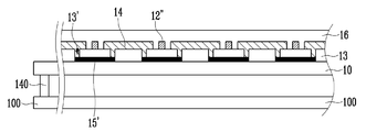
도 1은 본 발명의 실시예에 의한 평판표시장치의 상부기판에 대한 평면도.
도 2는 도 1의 특정 부분(A-A')에 대한 단면도.
도 3은 도 1에 대응되는 평판표시장치의 하부기판에 대한 평면도.
도 4는 절연막으로 사용되는 물질(산화실리콘, 포토아크릴, SOG)에 대한 광 투과율을 나타내는 그래프.
도 5a 내지 도 5c는 본 발명의 실시예에 의한 터치 스크린 패널 일체형 평판표시장치의 제조방법을 나타내는 공정 단면도.1 is a plan view of an upper substrate of a flat panel display device according to an exemplary embodiment of the present invention.
FIG. 2 is a cross-sectional view of a particular portion A-A 'of FIG. 1. FIG.
3 is a plan view of a lower substrate of the flat panel display device corresponding to FIG. 1.
4 is a graph showing the light transmittance of a material (silicon oxide, photoacrylic, SOG) used as an insulating film.
5A to 5C are cross-sectional views illustrating a method of manufacturing a touch screen panel integrated flat panel display according to an embodiment of the present invention.
이하, 첨부된 도면을 참조하여 본 발명의 실시예를 보다 상세히 설명하도록 한다. Hereinafter, embodiments of the present invention will be described in more detail with reference to the accompanying drawings.
도 1은 본 발명의 실시예에 의한 평판표시장치의 상부기판에 대한 평면도이고, 도 2는 도 1의 특정 부분(A-A')에 대한 단면도이다. 1 is a plan view of an upper substrate of a flat panel display device according to an exemplary embodiment of the present invention, and FIG. 2 is a cross-sectional view of a specific portion A-A 'of FIG. 1.
또한, 도 3은 도 1에 대응되는 평판표시장치의 하부기판에 대한 평면도이다.3 is a plan view of a lower substrate of the flat panel display device corresponding to FIG. 1.
도 1 및 도 2를 참조하면, 본 발명의 실시예에 의한 터치 스크린 패널은, 평판표시장치의 상부 기판(10) 상에 직접 형성됨을 특징으로 한다.1 and 2, the touch screen panel according to an exemplary embodiment of the present invention is directly formed on the
여기서, 상기 평판표시장치는 유기전계 발광 표시장치 또는 액정표시장치가 될 수 있으며, 본 발명의 실시예에서는 유기전계 발광 표시장치를 그 예로 설명하도록 하고, 이에 따라 상기 상부 기판(10)은 유기전계 발광 표시장치의 봉지 기판이며, 이는 투명 재질로 구현됨이 바람직하다.Here, the flat panel display device may be an organic light emitting display device or a liquid crystal display device, and in the exemplary embodiment of the present invention, the organic light emitting display device will be described as an example. An encapsulation substrate of the light emitting display device, which is preferably implemented by a transparent material.
본 발명의 실시예에 의한 터치 스크린 패널은 상기 상부기판 즉, 봉지기판의 제 1면 상에 형성된 다수의 감지패턴들(12, 14)과, 상기 감지패턴과 전기적으로 연결되는 금속패드들(15) 및 감지라인들(17)을 포함한다. The touch screen panel according to an embodiment of the present invention includes a plurality of
이 때, 상기 다수의 감지패턴들(12, 14)이 형성된 영역은 화상이 표시되어 터치 위치를 검출하는 표시 영역(20)이며, 상기 감지패턴과 전기적으로 연결되는 금속패드들(15), 감지라인(17)들 및 상기 각각의 감지라인들(17)과 연결되는 복수의 본딩 패드들(42)로 구성되는 FPC 본딩 패드부(40)가 형성된 영역은 상기 표시영역(20) 외곽에 구비되는 비표시 영역(30)이다.In this case, an area in which the plurality of
또한, 상기 비표시영역(30)에 대응되는 상부기판의 제 2면에는 상기 유기전계 발광 표시장치의 상부기판과 하부기판을 합착하기 위한 실링재(도 3의 140)가 도포된다. 즉, 상기 실링재(140)는 상부기판(10)과 하부기판(100) 사이에 형성되어 외기가 침투하지 못하도록 표시영역(20, 110)을 밀봉하는 역할을 수행한다.In addition, a sealing material (140 in FIG. 3) is formed on the second surface of the upper substrate corresponding to the
이 때, 상기 하부기판은 도 3에 도시된 바와 같이, 다수의 제 1 전극, 유기층 및 제 2 전극으로 구성되는 유기발광소자를 구비한 복수의 화소들(112)이 형성된 표시영역(110)과 표시영역(110)의 외곽에 형성되는 비표시영역(120)을 포함한다. In this case, as shown in FIG. 3, the lower substrate includes a
이 때, 표시영역(110)은 유기발광소자로부터 방출되는 빛으로 인해 소정의 화상이 표시되는 영역으로서, 행 방향으로 배열된 복수의 주사선(S1 내지 Sn) 및 열 방향으로 배열된 복수의 데이터선(D1 내지 Dm)을 포함하며, 주사선(S1 내지 Sm)과 데이터선(D1 내지 Dm)에 유기발광 소자를 구동하기 위한 구동회로(130, 132)부터 신호를 인가받는 복수의 화소(112)가 형성되어 있다.In this case, the
또한, 상기 비표시영역(120)은 상기 표시영역(110) 외곽에 구비되는 영역으로서, 상기 표시영역(110) 상에 형성된 다수의 화소(112)를 구동하기 위해 구동 회로 즉, 데이터 구동회로(132), 주사 구동회로(130)와, 상기 하부기판(100)과 상부기판(10)을 합착하는 실링재(140)가 형성된다. In addition, the
즉, 상기 하부기판(100)의 표시영역(110), 비표시영역(120)은 앞서 도 1에 도시된 상부기판(10)의 표시영역(20), 비표시영역(30)과 각각 중첩되도록 대응된다.That is, the
또한, 상기 상부기판(10)의 표시영역(20) 상에 형성된 감지패턴들은, 서로 교호적으로 배치되며 X 좌표가 동일한 하나의 열 또는 Y 좌표가 동일한 하나의 행 단위로 서로 연결되도록 형성된 제1 및 제2 감지패턴들(12, 14)을 포함한다. In addition, the first sensing patterns formed on the
즉, 제1 감지패턴들(12)은 제1 방향(열 방향)을 따라 X 좌표가 동일한 하나의 열에 배치된 제1 감지셀(12') 및 인접한 상기 제1 감지셀(12')을 연결하는 제1 연결라인(12")으로 구성되고, 제2 감지패턴들(14)은 제2 방향(행 방향)을 따라 Y 좌표가 동일한 하나의 행에 배치된 제2 감지셀(14)로 구성된다.That is, the
이 때, 본 발명의 실시예의 경우 상기 제1 감지패턴들(12) 및 제2 감지패턴들(14)은 동일 레이어(layer)에 형성되고, 상기 제1 및 제2 감지패턴들(12, 14)는 터치 스크린 패널의 동작 구현을 위해 투명 재질로 구현되어야 하며, 이에 상기 제1 및 제2 감지패턴들(12, 14)은 투명 도전성 물질, 일 예로 인듐-틴 옥사이드(이하, ITO)로 구현됨이 바람직하다.In this case, in the embodiment of the present invention, the
또한, 상기 제1 감지패턴들(12) 및 제2 감지패턴들(14)이 감지 전극으로서의 역할을 수행하기 위해서는 제 1방향 및 제2방향으로 배열된 각각의 감지셀들이 전기적으로 연결되어야 한다.In addition, in order for the
이에 상기 제1 감지셀(12')들은 제1 연결라인(12")에 의해 서로 전기적으로 연결되나, 상기 제2 감지패턴들을 구성하는 제2 감지셀(14)들은 상기 제1 감지셀(12')과 동일 레이어에 형성되기 때문에 상기 제1 연결라인(12')와 단락을 피하기 위해 상기 제1 연결라인과 교차되는 연결라인이 동일 레이어 상에는 형성될 수 없다.Accordingly, the
이에 본 발명의 실시예는 상기 각각의 제2 감지셀(14)을 전기적으로 연결하는 각각의 연결패턴(15')이 제1 감지패턴들(12)과는 다른 레이어에 형성되는 것으로, 제1 및 제2 감지패턴들(12, 14)의 하부 레이어에 형성됨을 특징으로 한다.Accordingly, in the embodiment of the present invention, each
즉, 본 발명의 실시예에 의한 터치 스크린 패널은 상부기판(10)으로서의 투명기판 상에 연결패턴(15')들이 형성되고, 상기 연결패턴(15')를 포함한 투명기판(11) 상에 제 1절연막(13)이 형성된다.That is, in the touch screen panel according to the embodiment of the present invention, the connection patterns 15 'are formed on the transparent substrate as the
이 때, 상기 연결패턴(15')들은 제1 및 제2 감지패턴들(12, 14)과 같은 ITO로 형성되거나, 상기 ITO보다 낮은 저항값을 갖는 금속 물질로 형성될 수 있다. In this case, the
또한, 상기 연결패턴(15')은 도시된 바와 같이 직사각형 바(bar) 형태로 이루어질 수 있으나, 이는 하나의 실시예로서 반드시 이러한 형상에 한정되지 않는다. 즉, 상기 절연막(13)의 콘택홀(13')에 의해 노출되는 부분인 연결패턴(15')의 끝단부의 폭이 상기 연결패턴(15')의 타 부위의 폭보다 넓은 형상으로 구현될 수도 있다.In addition, the
이와 같은 연결패턴(15')은 상기 제1 감지패턴들(12)의 제1 연결라인(12")과 서로 교차되는데, 상기 교차에 의해 발생되는 기생 캐패시턴스의 영향을 줄이기 위해 상기 연결패턴(15')의 폭을 최소화하는 것이 바람직하다.The
그러나, 이와 같이 상기 연결패턴(15')의 폭을 최소화할 경우 각각 제2 감지패턴들(14)의 라인 저항이 높아져 결과적으로 터치 스크린 패널의 기능을 구현하는 센싱 감도가 저하되는 문제가 발생한다.However, when the width of the connection pattern 15 'is minimized, the line resistance of each of the
이에 상기 연결패턴(15')은 저항이 낮은 도전성 물질로 형성함이 보다 바람직하다.Accordingly, the
이 경우, 상기 연결패턴(15')은 상기 제1 감지패턴들(12) 및 제2 감지패턴들(14)이 형성되는 영역의 가장자리 영역에 형성되어 감지된 신호를 구동회로(미도시) 측으로 공급하는 금속패드(15)와 동일한 재질로 형성되는 것으로, 상기 금속패드와 동일한 레이어에 동일 공정을 통해 형성되므로 상기 연결패턴(15')을 형성하기 위해 추가의 마스크 공정이 필요하지 않는다. In this case, the
따라서, 상기 연결패턴(15')을 상기 제1 및 제2 감지패턴들(12, 14)과 같은 투명 도전성 물질 물질로 형성하지 않아, 라인 저항이 높아짐을 방지함과 아울러 상기 연결패턴(15')을 형성하기 위해 마스크 공정이 추가되어야 하는 단점도 극복할 수 있음을 그 특징으로 한다. 또한, 상기 제 1 및 제 2감지패턴(12, 14) 상에는 제 2절연막(16)이 형성된다.
Therefore, the
앞서 설명한 바와 같이 본 발명의 실시예에 의한 터치 스크린 패널은 평판표시장치의 상부기판(10) 제 1면 상에 형성되며, 상기 상부기판의 비표시영역에 대응되는 제 2면에는 평판표시장치의 하부기판과 합착하기 위한 실링재가 도포된다.As described above, the touch screen panel according to the exemplary embodiment of the present invention is formed on the first surface of the
이 때, 상기 실링재(140)로는 고체 상태의 프릿(frit)을 사용할 수 있으며, 일반적으로 상기 프릿은 유리 분말에 산화물 분말을 포함한다.In this case, the sealing
또한, 산화물 분말이 포함된 프릿에 유기물을 첨가하여 젤 상태의 페이스트로 만들고, 그것을 400℃ 내지 500℃의 고온으로 소성한다. In addition, an organic substance is added to the frit containing the oxide powder to make a gel paste, and then fired at a high temperature of 400 ° C to 500 ° C.
이와 같이 상기 프릿을 소성하면 유기물은 공기 중으로 소멸되고, 젤 상태의 페이스트는 경화되어 고체 상태의 프릿으로 형성됨으로써, 상기 상부기판 및 하부기판을 합착하게 된다.When the frit is fired as described above, the organic substance is extinguished in the air, and the gel paste is cured to form a solid frit, thereby bonding the upper substrate and the lower substrate.
이 때, 상기 경화된 프릿에 레이저를 조사하여 이를 재차 용융하고 경화시키는 공정을 추가하여 상기 상, 하부기판의 합착 정도를 보다 더 견고히 할 수도 있다. At this time, the curing of the upper and lower substrates may be more firmly by adding a process of irradiating a laser to the cured frit and melting and curing it again.
즉, 본 발명의 실시예에 의한 터치 스크린 일체형 평판표시장치를 구현하기 위해서는 상, 하부기판의 밀봉을 위한 실링재(140)를 도포하고, 이에 대한 고온의 소성 공정이 수행되어야 한다.That is, in order to implement the touch screen integrated flat panel display device according to the embodiment of the present invention, the sealing
단, 상기 상부기판 및 하부기판의 밀봉을 수행하기에 앞서, 상기 상부기판의 제 1면 상에는 이미 터치 스크린 패널이 형성되어 있는데, 이 경우 상기 실링재(프릿)에 대한 고온의 소성 공정은 상기 상부기판(10)의 제 1면 상에 형성된 터치 스크린 패널을 구성하는 각 층에 영향을 미치게 된다.Before the sealing of the upper substrate and the lower substrate, the touch screen panel is already formed on the first surface of the upper substrate. In this case, the high temperature baking process for the sealing material (the frit) is performed on the upper substrate. Each layer constituting the touch screen panel formed on the first surface of 10 is affected.
따라서, 상기 터치 스크린 패널을 구성하는 제 1, 2절연막(13, 16)은 상기 고온의 소성 공정에서도 절연특성 등을 유지할 수 있는 재료로 형성되어야 하며, 이에 따라 산화실리콘(SiO2)과 같은 무기물 이외에 유기물로는 사용이 불가능하다는 단점이 있다.Therefore, the first and second insulating
또한, 상기 산화실리콘을 절연막으로 사용할 경우 일반적으로 2000 내지 4000Å의 두께로 구현되나, 이는 외부로부터 유입되는 ESD에 의한 불량을 방지하기에는 너무 얇다는 단점이 있으며, 이에 상기 산화실리콘막의 두께를 높이기 위해서는 성막 시간 및 드라이 에칭 시간 등이 상당히 증가되는 단점이 있다.
In addition, when the silicon oxide is used as an insulating film, it is generally implemented as a thickness of 2000 to 4000Å, which is disadvantageous in that it is too thin to prevent defects caused by ESD flowing from the outside. Thus, in order to increase the thickness of the silicon oxide film, There is a disadvantage in that the time, dry etching time, etc. are considerably increased.
이에 본 발명의 실시예에서는 이와 같은 단점을 극복하기 위하여 상기 터치 스크린 패널에 형성되는 제 1, 2절연막(13, 16)을 상기 실링재에 대한 고온 소성 공정에 적합한 안정적인 열특성을 갖는 스핀 온 글라스(Spin On Glass, 이하 SOG) 재질로 구현함을 특징으로 한다. Accordingly, in order to overcome such disadvantages, the first and second insulating
상기 SOG막은 스핀 코팅(spin coating) 방법으로 도포되는 것으로, 이는 실록세인(siloxane)계 화합물(예를 들면, (oligo) siloxane [실록세인결합 Si-O로 이루어져 있는 화합물의 총칭, 분자식 (H3Si)(n+1)On], organo-siloxane [실록세인결합에 Carbon기를 포함한 화합물의 총칭, 분자식 (CH3)(H2Si)(n+1)On], organo-alkoxysiloxan [실록세인결합에 Hydrocarbon기를 포함한 화합물의 총칭, 분자식 (CmH2m-1)(H2Si)(n+1)On], perfluoro-allkoxysiloxan [실록세인결합에 perfluorochain을 포함한 화합물의 총칭, 분자식 (CF3)n(CmH 2m-1)(H2Si)(n+1)On], siloxane 화합물에 UV 또는 열경화가 가능하도록 functional group인 methacrylate와 epoxy group이 포함됨), 실라젠(silozne)계 화합물 및 실리케이트(silicate)계 화합물, 실세스키옥세인(Silsesquioxane)계 화합물(Hydrogen Silsesquioxane(HSQ) 포함) 중에서 하나 이상의 화합물을 포함한다.The SOG film is applied by a spin coating method, which is a siloxane-based compound (for example, (oligo) siloxane [a compound composed of siloxane-bonded Si-O, generically referred to as molecular formula (H 3)). Si) (n + 1) O n ], organo-siloxane [collectively termed compound containing carbon group in siloxane bond, molecular formula (CH 3 ) (H 2 Si) (n + 1) O n ], organo-alkoxysiloxan [siloxane Generic term for compounds containing a hydrocarbon group in a bond, molecular formula (C m H 2m-1 ) (H 2 Si) (n + 1) O n ], perfluoro-allkoxysiloxan [generic term for compounds containing a perfluorochain to siloxane bond, molecular formula ( CF 3 ) n (C m H 2m-1 ) (H 2 Si) (n + 1) O n ], which includes functional groups methacrylate and epoxy group to enable UV or thermosetting to siloxane compounds, silazene ( at least one of silozne-based compounds, silicate-based compounds, and silsesquioxane-based compounds (including Hydrogen Silsesquioxane (HSQ)) It should.
또한, 이와 같은 화합물은 PGMEA(PROPYLENE GLYCOL MONOMETHYL ETHER ACETATE), PGME(polypropylene glycol methyl ether), MIBK(Methyl isobutyl ketone), NMP(N-Methyl-2-pyrrolidinone), NBA(Normal butyl acetate,) EL(Ethyl lactate) 등과 같은 에테르(ether), 아세테이트(acetate), 케톤(ketone) 계열의 용매(solvent)에 혼합되어 사용된다.In addition, such compounds are PGMEA (PROPYLENE GLYCOL MONOMETHYL ETHER ACETATE), PGME (polypropylene glycol methyl ether), MIBK (Methyl isobutyl ketone), NMP (N-Methyl-2-pyrrolidinone), NBA (Normal butyl acetate,) EL ( Ethyl lactate and the like (ether), acetate (acetate), ketone (ketone) -based solvent (solvent) is mixed and used.
이와 같은 SOG막은 단순한 코팅 방식을 통해 평탄한 절연막을 구현할 수 있다는 장점 이외에 앞서 언급한 바와 같이 고온 공정에도 절연 특성을 유지한다는 장점이 있으므로, 터치 스크린 패널이 상부기판 상에 일체형으로 구현되는 평판표시장치에 대하여 상기 터치 스크린 패널의 제 1, 2절연막(13, 16)으로 적용할 수 있다.As described above, the SOG film has a merit that a flat insulating film can be formed by a simple coating method, and thus, as described above, the SOG film maintains insulation characteristics even at a high temperature process. The first and second insulating
특히 SOG막은 스핀 코팅과 같은 단순한 코팅 방식으로 형성되기 때문에 그 두께를 쉽게 조절할 수 있는 바, 이를 통해 상기 터치 스크린 패널의 외부에서 인가되는 정전기에 대한 ESD 보호 측면에서 큰 장점이 있다.In particular, since the SOG film is formed by a simple coating method such as spin coating, the thickness thereof can be easily adjusted, thereby providing a great advantage in terms of ESD protection against static electricity applied from the outside of the touch screen panel.
절연막의 절연특성을 나타내는 수치인 BV(Break Voltage, 단위: MV/cm)는 기존의 산화실리콘막(SiO2)가 약 -7.34이고, SOG막은 -7.56으로 비슷한 정도를 나타내나, 하기된 [표 1]을 통해 확인되는 바와 같이 두께에 따른 ESD 불량 테스트 결과 얇은 두께로 구현되는 산화실리콘막에서 ESD 불량이 발생됨을 확인할 수 있다.BV (Break Voltage, MV / cm), which represents the insulation characteristics of the insulating film, is about -7.34 for the conventional silicon oxide film (SiO2) and about -7.56 for the SOG film. As can be seen from the ESD failure test according to the thickness it can be seen that the ESD failure occurs in the silicon oxide film is implemented in a thin thickness.
상기 [표 1]은 터치 스크린 패널에서 절연막으로 3000 Å의 산화실리콘막을 사용하는 경우와, 1um의 SOG막을 사용하는 경우에 대한 ESD 평가 결과를 나타내는 실험 데이터로서, 평가 대수는 10대이며, 터치 스크린 패널의 우상단 에지부의 표시영역에 ±1kV, ±1.5kV, ±2kV, ±2.5kV, ±3.0kV, ±3.5kV, ±4.0kV를 각각 5회씩 인가한 경우에 대한 것이다(평가규격: HBM(Human Body Model) R=1.5kΩ, C=100pF). [Table 1] is experimental data showing the results of ESD evaluation for the case of using a silicon oxide film of 3000 Å as the insulating film in the touch screen panel and the case of using a 1um SOG film, the number of evaluation is 10, touch screen This is the case of applying 5 times ± 1kV, ± 1.5kV, ± 2kV, ± 2.5kV, ± 3.0kV, ± 3.5kV, ± 4.0kV to the display area of the upper right edge of the panel (Evaluation standard: HBM (Human Body Model) R = 1.5kΩ, C = 100pF).
[표 1]에 의할 경우 3000 Å의 산화실리콘막이 사용될 경우 2kV 이상 정전기가 인가될 경우 모든 패널(10대)에서 불량이 발생되나, 1um의 SOG막을 사용할 경우에는 3.0kV까지의 정전기 유입에 대해서는 ESD 불량을 극복할 수 있음을 확인할 수 있다.According to [Table 1], when the 3000 Å silicon oxide film is used, if the static electricity is applied more than 2kV, the failure occurs in all panels (10 units) .However, when the 1um SOG film is used, the static electricity flows up to 3.0kV. It can be seen that ESD failure can be overcome.
즉, BV 특성이 유사하더라도 절연막의 두께를 두껍게 함으로써, ESD 불량을 극복할 수 있는데, 앞서 언급한 바와 같이 기존의 산화실리콘막은 약 2000 내지 4000Å의 두께로 구현되는 것으로 그 이상의 두께로 형성하기에는 성막 시간 및 드라이 에칭 시간 등이 상당히 증가되는 문제가 있어 실제 양품에는 약 3000Å의 두께로 구현되는 것이 현실이다.That is, even if the BV characteristics are similar, the thickness of the insulating film can be thickened to overcome the ESD failure. As mentioned above, the conventional silicon oxide film is realized at a thickness of about 2000 to 4000 kPa, and the film formation time is not sufficient to form a thickness higher than that. And there is a problem that the dry etching time, etc. is significantly increased, the actual product is implemented in a thickness of about 3000Å.
그러나, 이와 같은 두께로는 외부로부터 인가되는 정전기에 의한 ESD 불량을 극복하기 어렵다는 단점이 있으나, 본원발명에서와 같이 SOG막으로 절연막을 구현할 경우 스핀 코팅 방식을 통해 그 두께를 쉽게 조절할 수 있어 양품에서도 약 0.5um 내지 2um의 두께로 상기 SOG 재질의 절연막을 충분히 형성할 수 있는 것이다.However, such a thickness has a disadvantage in that it is difficult to overcome the ESD failure caused by static electricity applied from the outside, but in the case of implementing the insulating film with the SOG film as in the present invention, the thickness can be easily adjusted through spin coating method, even in good quality products. The insulating film of the SOG material can be sufficiently formed to a thickness of about 0.5um to 2um.
단, 상기 SOG막이 두껍게 형성됨에 따라 발생될 수 있는 광 투과율 저하는 도 4의 그래프 및 하기된 [표 2]의 결과를 통해 문제 없음을 확인할 수 있다.However, the decrease in the light transmittance that may occur as the SOG film is formed thick may be confirmed without problems through the graph of FIG. 4 and the results of Table 2 below.
도 4는 절연막으로 사용되는 물질(산화실리콘, 포토아크릴, SOG)에 대한 광 투과율을 나타내는 그래프이고, [표 2]는 파장별 투과율 정도를 나타내는 실험 데이터이다.4 is a graph showing the light transmittance of a material (silicon oxide, photoacryl, SOG) used as an insulating film, [Table 2] is experimental data showing the degree of transmittance for each wavelength.
1000ÅSilicon Oxide (SiO2)
1000Å
1umSOG
1um
(Photo Acryl)Organic insulating film
(Photo Acryl)
도 4 및 [표 2]를 참조하면, 1um의 두께를 갖는 SOG막의 경우도 약 90% 이상의 투과율을 나타내므로, 본 발명의 실시예에서와 같이 터치 스크린 패널의 제 1, 2절연막(13, 16)을 SOG막으로 구현할 경우 투과율 저하의 문제없이 ESD 불량을 개선하는 효과를 얻을 수 있게 된다. Referring to FIG. 4 and Table 2, the SOG film having a thickness of 1 μm also exhibits a transmittance of about 90% or more. Thus, as in the embodiment of the present invention, the first and second insulating
또한, 상기 SOG막은 연필 경도가 약 4H 이상이므로, 스크래치 불량 측면에서도 장점이 있다. In addition, since the SOG film has a pencil hardness of about 4H or more, there is an advantage in terms of scratch failure.
도 5a 내지 도 5c는 본 발명의 실시예에 의한 터치 스크린 패널 일체형 평판표시장치의 제조방법을 나타내는 공정 단면도이다.5A to 5C are cross-sectional views illustrating a method of manufacturing a touch screen panel integrated flat panel display according to an exemplary embodiment of the present invention.
단, 이는 표시패널의 일 영역과 비표시영역의 일 영역에 대한 단면을 중심으로 설명한다. However, this will be described based on a cross section of one area of the display panel and one area of the non-display area.
먼저 도 5a를 참조하면, 평판표시장치의 상부 기판(10) 상에 터치 스크린 패널이 형성된다.First, referring to FIG. 5A, a touch screen panel is formed on the
이 때, 상기 터치 스크린 패널의 단면 구조는 도 2에 도시된 단면도와 동일하므로, 구체적인 구성에 대한 설명은 생략하며, 도면부호는 동일하게 사용한다.In this case, since the cross-sectional structure of the touch screen panel is the same as the cross-sectional view shown in FIG. 2, a detailed description of the configuration is omitted and the same reference numerals are used.
단, 본 발명의 실시예의 경우 상기 터치 스크린 패널에 형성되는 제 1, 2절연막(13, 16)이 SOG막으로 구현됨을 특징으로 한다.However, in the exemplary embodiment of the present invention, the first and second insulating
특히 도 5a에 도시된 단계 즉, 상부기판 상에 터치 스크린 패널에 형성되는 단계에서 상기 제 1, 2절연막(13, 16)으로서의 SOG막은 소프트 베이킹 공정을 통해 150℃ 내지 250℃ 정도의 저온에서 가열하여 용매 성분을 제거한 상태로 구현된다.In particular, the SOG film as the first and second insulating
보다 구체적으로 설명하면, 상기 SOG막은 실록세인(siloxane)계 화합물, 실라젠(silozene)계 화합물 및 실리케이트(silicate)계 화합물, 실세스키옥세인(Silsesquioxane)계 화합물 중 하나 이상의 화합물을 포함한 고형분과 상기 고형분을 녹이는 용매가 혼합된 용액 상태로 상기 상부기판의 제 1면 상에 코팅된다.In more detail, the SOG film includes a solid content including at least one compound of a siloxane compound, a silozene compound, a silicate compound, and a silsesquioxane compound. The solvent dissolving the solid content is coated on the first surface of the upper substrate in a mixed solution state.
이후, 상기 용액은 저온의 소프트 베이킹 및 고온의 경화 공정을 통해 최종적인 SOG막이 형성되는데, 상기 도 5a에 도시된 단계에서는 상기 SOG 용액에 대하여 저온의 소프트 베이킹 공정만을 수행한 상태의 SOG막이 형성된다.Subsequently, the final SOG film is formed through a low temperature soft baking and a high temperature hardening process. In the step illustrated in FIG. 5A, a SOG film having a low temperature soft baking process is performed on the SOG solution. .
상기 소프트 베이킹 공정은 약 150 내지 250℃ 정도의 저온으로 진행되는데, 이를 통해 상기 SOG 용액의 용매가 제거된 가경화 상태의 SOG막이 형성되며, 이와 같은 가경화 상태의 SOG막도 기본적인 절연막 특성은 유지한다.The soft baking process is carried out at a low temperature of about 150 to 250 ℃, through which the SOG film of the temporary hardening state from which the solvent of the SOG solution is removed is formed, the basic insulating film properties of the SOG film of the temporary curing state is maintained do.
이후, 도 5b에 도시된 바와 같이 상부기판의 비표시영역에 대응되는 제 2면과 하부기판의 비표시영역에 실링재가 도포된다.Thereafter, as illustrated in FIG. 5B, a sealing material is applied to the second surface corresponding to the non-display area of the upper substrate and the non-display area of the lower substrate.
상기 하부기판의 구성은 앞서 도 3을 통해 설명한 바 있으므로 구체적인 설명은 생략한다. Since the configuration of the lower substrate has been described above with reference to FIG. 3, a detailed description thereof will be omitted.
여기서, 상기 실링재는 상부기판(10)과 하부기판(100) 사이에 형성되어 외기가 침투하지 못하도록 표시영역(20)을 밀봉하는 역할을 수행하는 것으로, 본 발명의 실시예의 경우 상기 실링재(140)로서 고체 상태의 프릿(frit)을 사용할 수 있다. Here, the sealing material is formed between the
이 때, 상기 프릿은 유리 분말에 산화물 분말을 포함하여 구성되고, 상기 산화물 분말이 포함된 프릿에 유기물을 첨가하여 젤 상태의 페이스트로 만들어 상기 비표시영역에 도포한다.At this time, the frit is composed of an oxide powder in the glass powder, the organic material is added to the frit containing the oxide powder to make a gel paste and applied to the non-display area.
다음으로 도 5c를 참조하면, 상기 실링재에 대하여 400℃ 내지 500℃의 고온으로 이를 소정하는 공정이 수행되며, 이와 같이 상기 프릿을 소성하면 유기물은 공기 중으로 소멸되고, 젤 상태의 페이스트는 경화되어 고체 상태의 프릿으로 형성됨으로써, 상기 상부기판 및 하부기판을 합착하게 된다.Next, referring to FIG. 5C, a process of determining the sealing material at a high temperature of 400 ° C. to 500 ° C. is performed. When the frit is fired, the organic material is extinguished in the air, and the gel paste is cured to form a solid. By forming the frit in the state, the upper substrate and the lower substrate is bonded.
또한, 앞서 설명한 바와 같이 상기 SOG막은 소프트 베이킹 공정과 고온의 경화 공정을 통해 최종 SOG막이 형성되는데, 본 발명의 실시예의 경우 상기 실링재에 대한 고온의 소성 공정 진행 시 상기 SOG 막의 경화 공정도 함께 수행됨을 특징으로 한다.In addition, as described above, the SOG film is a final SOG film formed through a soft baking process and a high temperature curing process. In the embodiment of the present invention, the SOG film curing process is also performed when the high temperature baking process is performed on the sealing material. It features.
즉, 도 5c의 공정을 통해 상부기판(10) 및 하부기판(100)이 합착되어 밀봉됨과 함께 상기 상부기판의 제 1면 상에 형성된 제 1, 2절연막(13, 16)으로서의 SOG막도 최종적으로 완전 경화되어 앞서 [표 1], [표 2]를 통해 설명한 SOG막의 특성을 발현할 수 있게 된다.That is, the SOG film as the first and second insulating
즉, 본 발명의 실시예에 의할 경우 터치 스크린 패널에 형성되는 SOG막의 고온 경화 공정을 상기 평판표시장치의 상, 하부기판의 밀봉 공정과 함께 구현함으로써, 공정시간 단축 및 공정비용 저감의 효과를 얻을 수 있다는 장점이 있다. That is, according to the exemplary embodiment of the present invention, the high temperature curing process of the SOG film formed on the touch screen panel is implemented together with the sealing process of the upper and lower substrates of the flat panel display device, thereby reducing the process time and reducing the process cost. This has the advantage of being available.
이상에서 설명한 본 발명은 상술한 실시 예 및 첨부된 도면에 한정되는 것이 아니고, 본 발명의 기술적 사상을 벗어나지 않는 범위 내에서 여러 가지 치환, 변형 및 변경이 가능하다는 것이 본 발명이 속하는 기술분야에서 종래의 지식을 가진 자에게 있어 명백할 것이다.It will be apparent to those skilled in the art that various modifications and variations can be made in the present invention without departing from the spirit or scope of the invention. Will be clear to those who have knowledge of.
10: 상부기판 12: 제 1감지패턴
13: 제 1절연막 14: 제 2감지패턴
15: 금속패드 15': 연결패턴
16: 제 2절연막 100: 하부기판
140: 실링재10: upper substrate 12: first sensing pattern
13: first insulating film 14: second sensing pattern
15: metal pad 15 ': connection pattern
16: second insulating film 100: lower substrate
140: sealing material
Claims (13)
상기 상부기판의 표시영역 상에 형성된 제 1 및 제 2감지패턴들과;
상기 제 2감지패턴들을 연결하는 연결패턴들과;
상기 연결패턴들 및 제 1감지패턴 사이에 형성되는 제 1절연막 및 상기 제 1, 2감지패턴들 상에 형성되는 제 2절연막과;
상기 상부기판 및 하부기판의 비표시영역 사이에 형성되는 실링재가 포함되고,
상기 제 1 및 제 2절연막은 스핀 온 글라스(SOG) 물질로 구현되며,
상기 하부기판은 다수의 제 1 전극, 유기층 및 제 2 전극으로 구성되는 유기발광소자를 구비한 복수의 화소들과, 상기 복수의 화소들을 구동하기 위한 구동 회로를 포함하여 구성되며,
상기 상부기판은 유기전계 발광 표시장치의 봉지기판임을 특징으로 하는 터치 스크린 패널 일체형 평판표시장치.An upper substrate and a lower substrate each divided into a display area and a non-display area formed outside the display area;
First and second sensing patterns formed on the display area of the upper substrate;
Connection patterns connecting the second sensing patterns;
A first insulating film formed between the connection patterns and the first sensing pattern and a second insulating film formed on the first and second sensing patterns;
It includes a sealing material formed between the non-display area of the upper substrate and the lower substrate,
The first and second insulating layers are made of a spin on glass (SOG) material.
The lower substrate includes a plurality of pixels including an organic light emitting element including a plurality of first electrodes, an organic layer, and a second electrode, and a driving circuit for driving the plurality of pixels.
And the upper substrate is an encapsulation substrate of an organic light emitting display device.
상기 스핀 온 글라스 물질은 실록세인(siloxane)계 화합물, 실라젠(silozene)계 화합물 및 실리케이트(silicate)계 화합물, 실세스키옥세인(Silsesquioxane)계 화합물 중 하나 이상의 화합물을 포함하여 구현됨을 특징으로 하는 터치 스크린 패널 일체형 평판표시장치.The method of claim 1,
The spin on glass material may be implemented by including one or more compounds of a siloxane-based compound, a silazene-based compound, a silicate-based compound, a silicate-based compound, and a silsesquioxane-based compound. Touch screen panel integrated flat panel display.
상기 제 1 및 제 2절연막은 두께가 0. 5um 내지 2um로 구현됨을 특징으로 하는 터치 스크린 패널 일체형 평판표시장치.The method of claim 1,
And the first and second insulating layers have a thickness of 0.5 μm to 2 μm.
상기 제1 감지패턴들은, 제1 방향을 따라 X 좌표가 동일한 하나의 열에 배치된 제1 감지셀 및 인접한 상기 제1 감지셀을 연결하는 제1 연결라인으로 구성됨을 특징으로 하는 터치 스크린 패널 일체형 평판표시장치.The method of claim 1,
The first sensing patterns may include a first sensing cell arranged in one column having the same X coordinate along a first direction, and a first connection line connecting the adjacent first sensing cells. Display.
상기 제2 감지패턴들은, 제2 방향을 따라 Y 좌표가 동일한 하나의 행에 배치된 제2 감지셀들로 구성됨을 특징으로 하는 터치 스크린 패널 일체형 평판표시장치.The method of claim 1,
And the second sensing patterns are formed of second sensing cells arranged in one row having the same Y coordinate along a second direction.
상기 제1 및 제2 감지패턴들이 형성되는 영역의 가장자리에 배치되어 상기 제1 및 제2 감지패턴들을 이에 대응되는 각각의 감지라인들과 전기적으로 연결하는 다수의 금속패턴들이 더 포함됨을 특징으로 하는 터치 스크린 패널 일체형 평판표시장치.The method of claim 1,
And a plurality of metal patterns disposed at an edge of a region where the first and second sensing patterns are formed to electrically connect the first and second sensing patterns to respective sensing lines corresponding thereto. Touch screen panel integrated flat panel display.
상기 다수의 연결패턴들 및 금속패턴들은 동일한 레이어 상에 형성되며, 상기 제1 및 제2 감지패턴들을 구현하는 물질보다 낮은 저항값을 갖는 물질로 구현됨을 특징으로 하는 터치 스크린 패널 일체형 평판표시장치.The method of claim 6,
The plurality of connection patterns and the metal patterns are formed on the same layer, and the touch screen panel integrated flat panel display device is formed of a material having a lower resistance value than a material implementing the first and second sensing patterns.
상기 제 1, 2절연막에 대하여 저온의 소프트 베이킹 공정이 수행되는 단계와;
상기 상부기판의 하면에 하부기판이 위치하고, 상기 상부기판 및 하부기판의 비표시영역 사이에 실링재가 도포되는 단계와;
상기 실링재에 대한 고온의 소성 공정 및 상기 제 1, 2절연막에 대한 고온의 경화 공정이 동시에 수행되는 단계가 포함되며,
상기 제 1 및 제 2절연막은 스핀 온 글라스(SOG) 물질로 구현됨을 특징으로 하는 터치 스크린 패널 일체형 평판표시장치의 제조방법.Forming a touch screen panel including connection patterns, first insulating layers, first and second sensing patterns, and second insulating layers on the display area of the upper substrate divided into a display area and a non-display area;
Performing a low temperature soft baking process on the first and second insulating films;
Placing a lower substrate on a lower surface of the upper substrate and applying a sealing material between the upper substrate and the non-display area of the lower substrate;
It includes the step of performing a high temperature baking process for the sealing material and a high temperature curing process for the first, second insulating film at the same time,
And the first and second insulating layers are formed of a spin on glass (SOG) material.
상기 스핀 온 글라스 물질은 실록세인(siloxane)계 화합물, 실라젠(silozene)계 화합물 및 실리케이트(silicate)계 화합물, 실세스키옥세인(Silsesquioxane)계 화합물 중 하나 이상의 화합물을 포함한 고형분과 상기 고형분을 녹이는 용매가 혼합된 용액 상태로 코팅되어 형성됨을 특징으로 하는 터치 스크린 패널 일체형 평판표시장치의 제조방법.The method of claim 9,
The spin-on glass material may include a solid containing at least one compound of a siloxane compound, a silozene compound, a silicate compound, a silicate compound, and a silsesquioxane compound to dissolve the solid content. Method of manufacturing a touch screen panel integrated flat panel display, characterized in that the solvent is formed by coating in a mixed solution state.
상기 소프트 베이킹 공정은 150℃ 내지 250℃의 온도에서 수행됨을 특징으로 하는 터치 스크린 패널 일체형 평판표시장치의 제조방법.The method of claim 9,
The soft baking process is a method of manufacturing a touch screen panel integrated flat panel display, characterized in that performed at a temperature of 150 ℃ to 250 ℃.
상기 고온의 소정 공정 및 고온의 경화 공정은 400℃ 내지 500℃의 온도에서 수행됨을 특징으로 하는 터치 스크린 패널 일체형 평판표시장치의 제조방법.The method of claim 9,
The high temperature predetermined process and the high temperature curing process is performed at a temperature of 400 ℃ to 500 ℃ manufacturing method of a touch screen panel integrated flat panel display.
상기 실링재는 산화물 분말이 포함된 프릿에 유기물을 첨가하여 젤 상태의 페이스트로 구현되어 상기 비표시영역에 도포됨을 특징으로 하는 터치 스크린 패널 일체형 평판표시장치의 제조방법.The method of claim 9,
The sealing material is a method of manufacturing a touch screen panel integrated flat panel display device, characterized in that the organic material is added to the frit containing the oxide powder is formed as a gel paste and applied to the non-display area.
Priority Applications (5)
| Application Number | Priority Date | Filing Date | Title |
|---|---|---|---|
| KR1020100030923A KR101073147B1 (en) | 2010-04-05 | 2010-04-05 | Touch screen panel integrated flat panel display and manufacturing method |
| JP2010153997A JP5587066B2 (en) | 2010-04-05 | 2010-07-06 | Flat screen display integrated with touch screen panel and method for manufacturing the same |
| US12/949,874 US20110242021A1 (en) | 2010-04-05 | 2010-11-19 | Flat panel display integrated touch screen panel and fabrication method thereof |
| CN201010599023.0A CN102214032B (en) | 2010-04-05 | 2010-12-10 | Flat-panel monitor of a kind of integrated touch screen panel and preparation method thereof |
| TW100101654A TWI559179B (en) | 2010-04-05 | 2011-01-17 | Flat panel display integrated touch screen panel and fabrication method thereof |
Applications Claiming Priority (1)
| Application Number | Priority Date | Filing Date | Title |
|---|---|---|---|
| KR1020100030923A KR101073147B1 (en) | 2010-04-05 | 2010-04-05 | Touch screen panel integrated flat panel display and manufacturing method |
Publications (1)
| Publication Number | Publication Date |
|---|---|
| KR101073147B1 true KR101073147B1 (en) | 2011-10-12 |
Family
ID=44709056
Family Applications (1)
| Application Number | Title | Priority Date | Filing Date |
|---|---|---|---|
| KR1020100030923A Active KR101073147B1 (en) | 2010-04-05 | 2010-04-05 | Touch screen panel integrated flat panel display and manufacturing method |
Country Status (5)
| Country | Link |
|---|---|
| US (1) | US20110242021A1 (en) |
| JP (1) | JP5587066B2 (en) |
| KR (1) | KR101073147B1 (en) |
| CN (1) | CN102214032B (en) |
| TW (1) | TWI559179B (en) |
Cited By (4)
| Publication number | Priority date | Publication date | Assignee | Title |
|---|---|---|---|---|
| US9367162B2 (en) | 2012-11-29 | 2016-06-14 | Samsung Display Co., Ltd. | Organic light emitting display apparatus having an encapsulation layer with a touch sensing layer and method of manufacturing the same |
| US10181295B2 (en) | 2015-10-23 | 2019-01-15 | Semiconductor Energy Laboratory Co., Ltd. | Semiconductor device and display panel comprising pixel having plurality of display elements |
| KR20190007140A (en) * | 2017-07-11 | 2019-01-22 | 삼성디스플레이 주식회사 | Touch display apparatus integrated fingerprint sensor |
| KR20200028328A (en) * | 2017-07-06 | 2020-03-16 | 제이에스알 가부시끼가이샤 | Light-emitting device and organic EL device, and manufacturing method thereof |
Families Citing this family (26)
| Publication number | Priority date | Publication date | Assignee | Title |
|---|---|---|---|---|
| US8791792B2 (en) | 2010-01-15 | 2014-07-29 | Idex Asa | Electronic imager using an impedance sensor grid array mounted on or about a switch and method of making |
| US8421890B2 (en) | 2010-01-15 | 2013-04-16 | Picofield Technologies, Inc. | Electronic imager using an impedance sensor grid array and method of making |
| US8866347B2 (en) | 2010-01-15 | 2014-10-21 | Idex Asa | Biometric image sensing |
| KR101357585B1 (en) * | 2011-12-08 | 2014-02-11 | 엘지이노텍 주식회사 | Conductive pattern of touch panel and forming method for the same |
| KR101974478B1 (en) * | 2012-01-09 | 2019-08-26 | 삼성디스플레이 주식회사 | Transparent laminate, window panel for display device and display device including the window panel |
| CN103309528A (en) * | 2012-03-16 | 2013-09-18 | 瀚宇彩晶股份有限公司 | Touch panel and manufacturing method thereof |
| JP2013196531A (en) * | 2012-03-22 | 2013-09-30 | Japan Display Inc | Touch panel and display device with touch panel |
| KR102245293B1 (en) | 2012-04-10 | 2021-04-28 | 이덱스 바이오메트릭스 아사 | Biometric Sensing |
| CN103458071B (en) * | 2012-06-05 | 2017-11-03 | 希姆通信息技术(上海)有限公司 | Handheld terminal and its manufacture method |
| KR101932164B1 (en) | 2012-07-17 | 2019-03-21 | 삼성디스플레이 주식회사 | touch screen panel and display device with the same |
| TWI514215B (en) * | 2012-11-22 | 2015-12-21 | Lg Innotek Co Ltd | Touch panel |
| KR102061108B1 (en) * | 2013-01-16 | 2020-01-02 | 삼성디스플레이 주식회사 | Organic Light Emitting Display integrated Touch Screen Panel |
| JP2014219963A (en) * | 2013-04-12 | 2014-11-20 | 信越ポリマー株式会社 | Sheet for sensor sheet production, method for producing the same, sensor sheet for touchpad, and method for producing the same |
| TWI483157B (en) * | 2013-04-23 | 2015-05-01 | Au Optronics Corp | Touch panel and touch display panel |
| TWI512582B (en) * | 2013-08-30 | 2015-12-11 | Au Optronics Corp | Touch panel and touch display panel |
| KR102144084B1 (en) * | 2013-11-19 | 2020-08-14 | 삼성디스플레이 주식회사 | display device integrated touch screen panel |
| KR102162912B1 (en) | 2013-12-06 | 2020-10-07 | 엘지디스플레이 주식회사 | Organic electroluminescent device having touch panel and method for fabricating the same |
| KR102237859B1 (en) * | 2014-05-14 | 2021-04-09 | 엘지이노텍 주식회사 | Touch panel and touch device with the same |
| CN104238823B (en) * | 2014-09-26 | 2017-08-25 | 上海天马微电子有限公司 | Touch display panel, preparation method thereof and touch display device |
| CN106299148B (en) * | 2015-06-10 | 2018-04-03 | 上海和辉光电有限公司 | The encapsulating structure and method for packing of display panel |
| KR102367990B1 (en) * | 2015-06-15 | 2022-02-28 | 삼성디스플레이 주식회사 | Flat display apparatus and method of manufacturing the same |
| KR101992915B1 (en) * | 2016-09-30 | 2019-06-25 | 엘지디스플레이 주식회사 | Organic light emitting display with touch sensor and fabricating method thereof |
| CN108268816A (en) * | 2016-12-30 | 2018-07-10 | 南昌欧菲生物识别技术有限公司 | Touch screen and electronic device with fingerprint identification function |
| KR102409433B1 (en) | 2017-11-03 | 2022-06-16 | 삼성디스플레이 주식회사 | Display device |
| CN110600427A (en) * | 2019-08-23 | 2019-12-20 | 武汉华星光电半导体显示技术有限公司 | Manufacturing method of flexible display device and flexible display device |
| CN117447234A (en) * | 2023-10-17 | 2024-01-26 | 夸泰克(广州)新材料有限责任公司 | A method for preparing ultra-high temperature resistant spin-coated glass film layer |
Citations (1)
| Publication number | Priority date | Publication date | Assignee | Title |
|---|---|---|---|---|
| KR100720097B1 (en) | 2001-02-13 | 2007-05-18 | 삼성전자주식회사 | Liquid Crystal Display and Manufacturing Method Thereof |
Family Cites Families (23)
| Publication number | Priority date | Publication date | Assignee | Title |
|---|---|---|---|---|
| JP2006229221A (en) * | 1994-03-11 | 2006-08-31 | Kawasaki Microelectronics Kk | Coating solution for insulating film formation and method for forming insulating film for semiconductor device |
| JP2000058642A (en) * | 1998-08-07 | 2000-02-25 | Toshiba Corp | Method for manufacturing semiconductor device |
| KR100492157B1 (en) * | 2003-02-18 | 2005-06-02 | 삼성전자주식회사 | Method of forming silicon oxide layer in semiconductor manufacturing process |
| JP3913534B2 (en) * | 2001-11-30 | 2007-05-09 | 株式会社半導体エネルギー研究所 | Display device and display system using the same |
| US7369111B2 (en) * | 2003-04-29 | 2008-05-06 | Samsung Electronics Co., Ltd. | Gate driving circuit and display apparatus having the same |
| JP4772791B2 (en) * | 2005-07-11 | 2011-09-14 | シャープ株式会社 | Liquid crystal display device and manufacturing method thereof |
| CN101410779A (en) * | 2006-06-12 | 2009-04-15 | 夏普株式会社 | Touch panel, display device and touch panel manufacturing method |
| JP4564472B2 (en) * | 2006-07-11 | 2010-10-20 | エルジー ディスプレイ カンパニー リミテッド | Liquid crystal display device and manufacturing method thereof |
| JP2008065748A (en) * | 2006-09-11 | 2008-03-21 | Sharp Corp | Touch panel and display device using touch panel |
| WO2008032476A1 (en) * | 2006-09-11 | 2008-03-20 | Sharp Kabushiki Kaisha | Display device provided with touch panel |
| TW200842681A (en) * | 2007-04-27 | 2008-11-01 | Tpk Touch Solutions Inc | Touch pattern structure of a capacitive touch panel |
| TW200844827A (en) * | 2007-05-11 | 2008-11-16 | Sense Pad Tech Co Ltd | Transparent touch panel device |
| JP4506785B2 (en) * | 2007-06-14 | 2010-07-21 | エプソンイメージングデバイス株式会社 | Capacitive input device |
| JP5212063B2 (en) * | 2007-12-27 | 2013-06-19 | 住友化学株式会社 | Photosensitive resin composition |
| JP2009265748A (en) * | 2008-04-22 | 2009-11-12 | Hitachi Displays Ltd | Display with touch panel |
| CN101566758B (en) * | 2008-04-25 | 2011-05-04 | 清华大学 | Liquid crystal display |
| KR20100006987A (en) * | 2008-07-11 | 2010-01-22 | 삼성모바일디스플레이주식회사 | Touch screen panel and fabricating method for the same |
| JP5178379B2 (en) * | 2008-07-31 | 2013-04-10 | 株式会社ジャパンディスプレイイースト | Display device |
| WO2010029979A1 (en) * | 2008-09-12 | 2010-03-18 | オプトレックス株式会社 | Electrostatic capacity type touch panel, display device, and electrostatic capacity type touch panel manufacturing method |
| KR101002308B1 (en) * | 2008-09-12 | 2010-12-17 | 엘지디스플레이 주식회사 | Liquid crystal display |
| US8624845B2 (en) * | 2008-09-26 | 2014-01-07 | Cypress Semiconductor Corporation | Capacitance touch screen |
| KR101048930B1 (en) * | 2009-01-16 | 2011-07-12 | 삼성모바일디스플레이주식회사 | Touch screen panel |
| JP5534174B2 (en) * | 2010-01-21 | 2014-06-25 | 大日本印刷株式会社 | Touch panel member, and display device and touch panel using the touch panel member |
-
2010
- 2010-04-05 KR KR1020100030923A patent/KR101073147B1/en active Active
- 2010-07-06 JP JP2010153997A patent/JP5587066B2/en active Active
- 2010-11-19 US US12/949,874 patent/US20110242021A1/en not_active Abandoned
- 2010-12-10 CN CN201010599023.0A patent/CN102214032B/en active Active
-
2011
- 2011-01-17 TW TW100101654A patent/TWI559179B/en active
Patent Citations (1)
| Publication number | Priority date | Publication date | Assignee | Title |
|---|---|---|---|---|
| KR100720097B1 (en) | 2001-02-13 | 2007-05-18 | 삼성전자주식회사 | Liquid Crystal Display and Manufacturing Method Thereof |
Cited By (7)
| Publication number | Priority date | Publication date | Assignee | Title |
|---|---|---|---|---|
| US9367162B2 (en) | 2012-11-29 | 2016-06-14 | Samsung Display Co., Ltd. | Organic light emitting display apparatus having an encapsulation layer with a touch sensing layer and method of manufacturing the same |
| US9696838B2 (en) | 2012-11-29 | 2017-07-04 | Samsung Display Co., Ltd. | Organic light emitting display apparatus having a touch sensing layer and method of manufacturing the same |
| US10181295B2 (en) | 2015-10-23 | 2019-01-15 | Semiconductor Energy Laboratory Co., Ltd. | Semiconductor device and display panel comprising pixel having plurality of display elements |
| KR20200028328A (en) * | 2017-07-06 | 2020-03-16 | 제이에스알 가부시끼가이샤 | Light-emitting device and organic EL device, and manufacturing method thereof |
| KR102632744B1 (en) * | 2017-07-06 | 2024-02-01 | 제이에스알 가부시끼가이샤 | Light-emitting devices and organic EL devices, and methods for manufacturing them |
| KR20190007140A (en) * | 2017-07-11 | 2019-01-22 | 삼성디스플레이 주식회사 | Touch display apparatus integrated fingerprint sensor |
| KR102364418B1 (en) * | 2017-07-11 | 2022-02-18 | 삼성디스플레이 주식회사 | Touch display apparatus integrated fingerprint sensor |
Also Published As
| Publication number | Publication date |
|---|---|
| TWI559179B (en) | 2016-11-21 |
| JP5587066B2 (en) | 2014-09-10 |
| TW201135556A (en) | 2011-10-16 |
| US20110242021A1 (en) | 2011-10-06 |
| CN102214032B (en) | 2016-05-11 |
| JP2011221477A (en) | 2011-11-04 |
| CN102214032A (en) | 2011-10-12 |
Similar Documents
| Publication | Publication Date | Title |
|---|---|---|
| KR101073147B1 (en) | Touch screen panel integrated flat panel display and manufacturing method | |
| TWI517377B (en) | Organic light emitting display and method of manufacturing same | |
| JP5525589B2 (en) | Organic light-emitting display device and method for manufacturing the same | |
| TWI549287B (en) | Organic light emitting display device | |
| JP5284544B2 (en) | Semiconductor device and display device | |
| KR100768905B1 (en) | An electroluminescence device and an electronic apparatus | |
| US10599241B2 (en) | Touch panel and method for manufacturing the same, display apparatus | |
| CN103631458B (en) | Touch panel, its electronic device and its manufacturing method | |
| TWI519852B (en) | Touch display device | |
| KR20130072591A (en) | Liquid crystal display device and method for manufacturing the same | |
| KR101452955B1 (en) | Touch sensing device and manufacturing method thereof | |
| CN103019445B (en) | touch panel and touch display panel | |
| CN102447075B (en) | Display panel | |
| KR101779906B1 (en) | Film touch sensor | |
| JP2015043112A (en) | Touch panel and display device with touch panel | |
| CN204759388U (en) | Touch control device | |
| KR101472961B1 (en) | Touch sensing electrode | |
| US20110317115A1 (en) | Liquid crystal display device and method for manufacturing same | |
| KR101250320B1 (en) | In-plane switching mode liquid crystal display device having touch sensing function and method of fabricating the same | |
| CN107046041B (en) | Flexible array substrate, manufacturing method thereof, and flexible display device | |
| KR20120096235A (en) | In-plane switching mode liquid crystal display device having touch sensing function and method of fabricating the same | |
| JP2013041471A (en) | Touch panel member, display device with touch panel, and touch panel | |
| KR102003844B1 (en) | In-plain switching mode liquid crystal display device and method of fabricating the same | |
| KR20180100510A (en) | Organic light emitting display with touch sensor | |
| KR20180093339A (en) | Touch sensor and method of manufacturing the same |
Legal Events
| Date | Code | Title | Description |
|---|---|---|---|
| A201 | Request for examination | ||
| PA0109 | Patent application |
Patent event code: PA01091R01D Comment text: Patent Application Patent event date: 20100405 |
|
| PA0201 | Request for examination | ||
| E902 | Notification of reason for refusal | ||
| PE0902 | Notice of grounds for rejection |
Comment text: Notification of reason for refusal Patent event date: 20110624 Patent event code: PE09021S01D |
|
| E701 | Decision to grant or registration of patent right | ||
| PE0701 | Decision of registration |
Patent event code: PE07011S01D Comment text: Decision to Grant Registration Patent event date: 20110930 |
|
| GRNT | Written decision to grant | ||
| PR0701 | Registration of establishment |
Comment text: Registration of Establishment Patent event date: 20111006 Patent event code: PR07011E01D |
|
| PR1002 | Payment of registration fee |
Payment date: 20111006 End annual number: 3 Start annual number: 1 |
|
| PG1601 | Publication of registration | ||
| FPAY | Annual fee payment |
Payment date: 20141001 Year of fee payment: 4 |
|
| PR1001 | Payment of annual fee |
Payment date: 20141001 Start annual number: 4 End annual number: 4 |
|
| FPAY | Annual fee payment |
Payment date: 20170928 Year of fee payment: 7 |
|
| PR1001 | Payment of annual fee |
Payment date: 20170928 Start annual number: 7 End annual number: 7 |
|
| FPAY | Annual fee payment |
Payment date: 20181001 Year of fee payment: 8 |
|
| PR1001 | Payment of annual fee |
Payment date: 20181001 Start annual number: 8 End annual number: 8 |
|
| FPAY | Annual fee payment |
Payment date: 20191001 Year of fee payment: 9 |
|
| PR1001 | Payment of annual fee |
Payment date: 20191001 Start annual number: 9 End annual number: 9 |
|
| PR1001 | Payment of annual fee |
Payment date: 20201005 Start annual number: 10 End annual number: 10 |
|
| PR1001 | Payment of annual fee |
Payment date: 20210927 Start annual number: 11 End annual number: 11 |
|
| PR1001 | Payment of annual fee |
Payment date: 20230925 Start annual number: 13 End annual number: 13 |
|
| PR1001 | Payment of annual fee |