KR101047088B1 - Device temperature control and pattern compensation device method - Google Patents
Device temperature control and pattern compensation device method Download PDFInfo
- Publication number
- KR101047088B1 KR101047088B1 KR1020087010503A KR20087010503A KR101047088B1 KR 101047088 B1 KR101047088 B1 KR 101047088B1 KR 1020087010503 A KR1020087010503 A KR 1020087010503A KR 20087010503 A KR20087010503 A KR 20087010503A KR 101047088 B1 KR101047088 B1 KR 101047088B1
- Authority
- KR
- South Korea
- Prior art keywords
- substrate
- processing system
- substrate processing
- temperature
- emissivity
- Prior art date
- Legal status (The legal status is an assumption and is not a legal conclusion. Google has not performed a legal analysis and makes no representation as to the accuracy of the status listed.)
- Active
Links
- 238000000034 method Methods 0.000 title claims description 41
- 239000000758 substrate Substances 0.000 claims abstract description 211
- 238000010438 heat treatment Methods 0.000 claims abstract description 58
- 238000012545 processing Methods 0.000 claims abstract description 50
- 230000002093 peripheral effect Effects 0.000 claims abstract description 49
- 230000003287 optical effect Effects 0.000 claims description 71
- 239000000523 sample Substances 0.000 claims description 69
- 230000005855 radiation Effects 0.000 claims description 37
- 230000008569 process Effects 0.000 claims description 21
- 238000009826 distribution Methods 0.000 claims description 9
- 239000000463 material Substances 0.000 claims description 3
- 239000010408 film Substances 0.000 description 40
- 235000012431 wafers Nutrition 0.000 description 16
- VYPSYNLAJGMNEJ-UHFFFAOYSA-N silicon dioxide Inorganic materials O=[Si]=O VYPSYNLAJGMNEJ-UHFFFAOYSA-N 0.000 description 12
- 230000000694 effects Effects 0.000 description 11
- 235000012239 silicon dioxide Nutrition 0.000 description 11
- 239000010453 quartz Substances 0.000 description 10
- 238000005259 measurement Methods 0.000 description 9
- OKTJSMMVPCPJKN-UHFFFAOYSA-N Carbon Chemical compound [C] OKTJSMMVPCPJKN-UHFFFAOYSA-N 0.000 description 8
- 238000000151 deposition Methods 0.000 description 8
- 230000008021 deposition Effects 0.000 description 8
- 229910002804 graphite Inorganic materials 0.000 description 8
- 239000010439 graphite Substances 0.000 description 8
- 238000009529 body temperature measurement Methods 0.000 description 7
- 239000003507 refrigerant Substances 0.000 description 7
- XUIMIQQOPSSXEZ-UHFFFAOYSA-N Silicon Chemical compound [Si] XUIMIQQOPSSXEZ-UHFFFAOYSA-N 0.000 description 5
- 238000006243 chemical reaction Methods 0.000 description 5
- 239000007789 gas Substances 0.000 description 5
- 229910052710 silicon Inorganic materials 0.000 description 5
- 239000010703 silicon Substances 0.000 description 5
- 230000008859 change Effects 0.000 description 4
- 230000002708 enhancing effect Effects 0.000 description 4
- 238000012360 testing method Methods 0.000 description 4
- 239000000835 fiber Substances 0.000 description 3
- 230000001965 increasing effect Effects 0.000 description 3
- 230000036961 partial effect Effects 0.000 description 3
- HBMJWWWQQXIZIP-UHFFFAOYSA-N silicon carbide Chemical compound [Si+]#[C-] HBMJWWWQQXIZIP-UHFFFAOYSA-N 0.000 description 3
- 229910010271 silicon carbide Inorganic materials 0.000 description 3
- 229910000831 Steel Inorganic materials 0.000 description 2
- 230000000295 complement effect Effects 0.000 description 2
- 238000001816 cooling Methods 0.000 description 2
- 238000013461 design Methods 0.000 description 2
- 238000004519 manufacturing process Methods 0.000 description 2
- 238000012544 monitoring process Methods 0.000 description 2
- 239000012788 optical film Substances 0.000 description 2
- 229910021420 polycrystalline silicon Inorganic materials 0.000 description 2
- 229920005591 polysilicon Polymers 0.000 description 2
- 239000007787 solid Substances 0.000 description 2
- 239000010959 steel Substances 0.000 description 2
- 239000010409 thin film Substances 0.000 description 2
- 229910052581 Si3N4 Inorganic materials 0.000 description 1
- 229910000577 Silicon-germanium Inorganic materials 0.000 description 1
- LEVVHYCKPQWKOP-UHFFFAOYSA-N [Si].[Ge] Chemical compound [Si].[Ge] LEVVHYCKPQWKOP-UHFFFAOYSA-N 0.000 description 1
- 238000002835 absorbance Methods 0.000 description 1
- 239000002250 absorbent Substances 0.000 description 1
- 230000002745 absorbent Effects 0.000 description 1
- 239000006096 absorbing agent Substances 0.000 description 1
- 238000010521 absorption reaction Methods 0.000 description 1
- 230000002411 adverse Effects 0.000 description 1
- XAGFODPZIPBFFR-UHFFFAOYSA-N aluminium Chemical compound [Al] XAGFODPZIPBFFR-UHFFFAOYSA-N 0.000 description 1
- 229910052782 aluminium Inorganic materials 0.000 description 1
- PNEYBMLMFCGWSK-UHFFFAOYSA-N aluminium oxide Inorganic materials [O-2].[O-2].[O-2].[Al+3].[Al+3] PNEYBMLMFCGWSK-UHFFFAOYSA-N 0.000 description 1
- 238000013459 approach Methods 0.000 description 1
- 238000000149 argon plasma sintering Methods 0.000 description 1
- 238000004364 calculation method Methods 0.000 description 1
- 229910010293 ceramic material Inorganic materials 0.000 description 1
- 238000005234 chemical deposition Methods 0.000 description 1
- 230000000052 comparative effect Effects 0.000 description 1
- 230000001010 compromised effect Effects 0.000 description 1
- 239000004020 conductor Substances 0.000 description 1
- 238000012937 correction Methods 0.000 description 1
- 230000007547 defect Effects 0.000 description 1
- PCHJSUWPFVWCPO-UHFFFAOYSA-N gold Chemical compound [Au] PCHJSUWPFVWCPO-UHFFFAOYSA-N 0.000 description 1
- 239000010931 gold Substances 0.000 description 1
- 229910052737 gold Inorganic materials 0.000 description 1
- 230000006872 improvement Effects 0.000 description 1
- 230000006698 induction Effects 0.000 description 1
- 230000007246 mechanism Effects 0.000 description 1
- 229910021421 monocrystalline silicon Inorganic materials 0.000 description 1
- 238000004886 process control Methods 0.000 description 1
- 238000009789 rate limiting process Methods 0.000 description 1
- 239000000376 reactant Substances 0.000 description 1
- 230000002829 reductive effect Effects 0.000 description 1
- 238000002310 reflectometry Methods 0.000 description 1
- 229910052594 sapphire Inorganic materials 0.000 description 1
- 239000010980 sapphire Substances 0.000 description 1
- 239000000377 silicon dioxide Substances 0.000 description 1
- HQVNEWCFYHHQES-UHFFFAOYSA-N silicon nitride Chemical compound N12[Si]34N5[Si]62N3[Si]51N64 HQVNEWCFYHHQES-UHFFFAOYSA-N 0.000 description 1
- 239000012686 silicon precursor Substances 0.000 description 1
- 239000000126 substance Substances 0.000 description 1
- 239000002470 thermal conductor Substances 0.000 description 1
- ZDHXKXAHOVTTAH-UHFFFAOYSA-N trichlorosilane Chemical compound Cl[SiH](Cl)Cl ZDHXKXAHOVTTAH-UHFFFAOYSA-N 0.000 description 1
- 239000005052 trichlorosilane Substances 0.000 description 1
Images


Classifications
-
- C—CHEMISTRY; METALLURGY
- C23—COATING METALLIC MATERIAL; COATING MATERIAL WITH METALLIC MATERIAL; CHEMICAL SURFACE TREATMENT; DIFFUSION TREATMENT OF METALLIC MATERIAL; COATING BY VACUUM EVAPORATION, BY SPUTTERING, BY ION IMPLANTATION OR BY CHEMICAL VAPOUR DEPOSITION, IN GENERAL; INHIBITING CORROSION OF METALLIC MATERIAL OR INCRUSTATION IN GENERAL
- C23C—COATING METALLIC MATERIAL; COATING MATERIAL WITH METALLIC MATERIAL; SURFACE TREATMENT OF METALLIC MATERIAL BY DIFFUSION INTO THE SURFACE, BY CHEMICAL CONVERSION OR SUBSTITUTION; COATING BY VACUUM EVAPORATION, BY SPUTTERING, BY ION IMPLANTATION OR BY CHEMICAL VAPOUR DEPOSITION, IN GENERAL
- C23C16/00—Chemical coating by decomposition of gaseous compounds, without leaving reaction products of surface material in the coating, i.e. chemical vapour deposition [CVD] processes
- C23C16/44—Chemical coating by decomposition of gaseous compounds, without leaving reaction products of surface material in the coating, i.e. chemical vapour deposition [CVD] processes characterised by the method of coating
- C23C16/46—Chemical coating by decomposition of gaseous compounds, without leaving reaction products of surface material in the coating, i.e. chemical vapour deposition [CVD] processes characterised by the method of coating characterised by the method used for heating the substrate
-
- C—CHEMISTRY; METALLURGY
- C23—COATING METALLIC MATERIAL; COATING MATERIAL WITH METALLIC MATERIAL; CHEMICAL SURFACE TREATMENT; DIFFUSION TREATMENT OF METALLIC MATERIAL; COATING BY VACUUM EVAPORATION, BY SPUTTERING, BY ION IMPLANTATION OR BY CHEMICAL VAPOUR DEPOSITION, IN GENERAL; INHIBITING CORROSION OF METALLIC MATERIAL OR INCRUSTATION IN GENERAL
- C23C—COATING METALLIC MATERIAL; COATING MATERIAL WITH METALLIC MATERIAL; SURFACE TREATMENT OF METALLIC MATERIAL BY DIFFUSION INTO THE SURFACE, BY CHEMICAL CONVERSION OR SUBSTITUTION; COATING BY VACUUM EVAPORATION, BY SPUTTERING, BY ION IMPLANTATION OR BY CHEMICAL VAPOUR DEPOSITION, IN GENERAL
- C23C16/00—Chemical coating by decomposition of gaseous compounds, without leaving reaction products of surface material in the coating, i.e. chemical vapour deposition [CVD] processes
- C23C16/44—Chemical coating by decomposition of gaseous compounds, without leaving reaction products of surface material in the coating, i.e. chemical vapour deposition [CVD] processes characterised by the method of coating
- C23C16/48—Chemical coating by decomposition of gaseous compounds, without leaving reaction products of surface material in the coating, i.e. chemical vapour deposition [CVD] processes characterised by the method of coating by irradiation, e.g. photolysis, radiolysis, particle radiation
- C23C16/481—Chemical coating by decomposition of gaseous compounds, without leaving reaction products of surface material in the coating, i.e. chemical vapour deposition [CVD] processes characterised by the method of coating by irradiation, e.g. photolysis, radiolysis, particle radiation by radiant heating of the substrate
-
- C—CHEMISTRY; METALLURGY
- C23—COATING METALLIC MATERIAL; COATING MATERIAL WITH METALLIC MATERIAL; CHEMICAL SURFACE TREATMENT; DIFFUSION TREATMENT OF METALLIC MATERIAL; COATING BY VACUUM EVAPORATION, BY SPUTTERING, BY ION IMPLANTATION OR BY CHEMICAL VAPOUR DEPOSITION, IN GENERAL; INHIBITING CORROSION OF METALLIC MATERIAL OR INCRUSTATION IN GENERAL
- C23C—COATING METALLIC MATERIAL; COATING MATERIAL WITH METALLIC MATERIAL; SURFACE TREATMENT OF METALLIC MATERIAL BY DIFFUSION INTO THE SURFACE, BY CHEMICAL CONVERSION OR SUBSTITUTION; COATING BY VACUUM EVAPORATION, BY SPUTTERING, BY ION IMPLANTATION OR BY CHEMICAL VAPOUR DEPOSITION, IN GENERAL
- C23C16/00—Chemical coating by decomposition of gaseous compounds, without leaving reaction products of surface material in the coating, i.e. chemical vapour deposition [CVD] processes
- C23C16/44—Chemical coating by decomposition of gaseous compounds, without leaving reaction products of surface material in the coating, i.e. chemical vapour deposition [CVD] processes characterised by the method of coating
- C23C16/52—Controlling or regulating the coating process
Landscapes
- Chemical & Material Sciences (AREA)
- General Chemical & Material Sciences (AREA)
- Chemical Kinetics & Catalysis (AREA)
- Engineering & Computer Science (AREA)
- Materials Engineering (AREA)
- Mechanical Engineering (AREA)
- Metallurgy (AREA)
- Organic Chemistry (AREA)
- Health & Medical Sciences (AREA)
- Toxicology (AREA)
- Chemical Vapour Deposition (AREA)
- Physical Vapour Deposition (AREA)
Abstract
필름 형성 시스템은 상부 커버 및 측벽에 의해 경계를 형성하는 처리 챔버를 포함한다. 일 실시예에서, 서셉터는 상기 시스템에 회전가능하게 배치되고, 측벽 주위에 배치되는 제 1 주변 부재와 중첩된다. 방사 가열 시스템이 기판을 가열하기 위해 서셉터 아래 배치된다. 또 다른 실시예에서, 상부 커버는 다수의 존에 걸쳐 기판의 온도를 측정하기 위해 균일하게 이격된 고온계를 가진다. 기판의 온도는 고온계의 데이터로부터 얻어진다.

The film forming system includes a processing chamber that is bounded by a top cover and sidewalls. In one embodiment, the susceptor is rotatably disposed in the system and overlaps with a first peripheral member disposed around the sidewall. A radiant heating system is placed below the susceptor to heat the substrate. In another embodiment, the top cover has a pyrometer evenly spaced to measure the temperature of the substrate over the multiple zones. The temperature of the substrate is obtained from the data of the pyrometer.
Description
본 발명의 실시예들은 일반적으로 반응 챔버 및 필름 형성 장치 및 방법에 관한 것이다.Embodiments of the present invention generally relate to reaction chambers and film forming apparatus and methods.
지난 수년에 걸쳐, 다양한 분야에서 단결정 실리콘 필름의 저온 증착에 대한 요구가 증가되었다. 이 같은 분야의 예는 블랭킷 실리콘 게르마늄 필름, 상승형 및/또는 리세스형 소스 드레인 선택 증착, 다른 인장 또는 압축 변형을 하는 필름, 등을 포함하지만, 이에 제한되는 것은 아니다. 특별한 분야에 따라, 이러한 공정들은 모두 필름을 성장시키기 위해 이용되는 압력, 온도 및 화학물이 상당히 상이하다. 그러나, 이러한 공정들이 공통으로 가지는 하나의 요구조건은 공정들이 모두 웨이퍼 온도의 매우 안전하고, 정확하고 균일한 제어를 요구한다는 것이다.Over the years, the demand for low temperature deposition of single crystal silicon films in various fields has increased. Examples in this field include, but are not limited to, blanket silicon germanium films, raised and / or recessed source drain selective deposition, films with other tensile or compressive strains, and the like. Depending on the particular field, these processes all differ significantly in the pressure, temperature and chemicals used to grow the film. However, one requirement that these processes have in common is that they all require very safe, accurate and uniform control of wafer temperature.
단일 웨이퍼 실리콘 증착 CVD 챔버(200 mm 및 300 mm 분야 둘다에 대해)는 현재 다년 동안 이용가능하였다. 그러나, 이러한 장비는 주로 고온(약 1100℃) 블랭킷 대기 에피택셜 상태로 설계되었다. 이러한 고온 분야로부터 더 새롭고 더 낮은 온도 분야로 이동할 때 이 같은 장비의 성능에 충격을 가하는 몇 개의 요소가 있다.Single wafer silicon deposition CVD chambers (for both 200 mm and 300 mm applications) have been available for many years now. However, this equipment was designed primarily for high temperature (about 1100 ° C.) blanket atmospheric epitaxial conditions. There are several factors that impact the performance of such equipment when moving from these high temperature areas to newer and lower temperature areas.
첫 번째, 실리콘 전구체 가스로서 트리클로로실란을 이용하는 고온 대기 에피택셜 분야는 대량-운반 제한 공정(mass-transport limited process)이다. 이는 반응물이 표면으로 전달되는 속도에 비해 화학적 증착 반응이 매우 신속하게 발생하는 것을 의미하며, 실리콘 필름의 균일도를 결정하는 주요 인자는 가스 유동의 균일도이다. 이 같은 분야에서 온도 제어는 제 2 인자이다. 예를 들면, 통상적인 3 미크론 1130℃ 대기 에피택셜 공정에 대해, 각각의 섭씨 온도 에러(degree Celcious of temperature error)(전체 또는 웨이퍼에 걸쳐)는 0.004 미크론 또는 단지 0.13%의 필름 두께 편차를 형성한다. 1σ에 대해 약 0.8%의 통상적인 산업 균일도 요구조건에서, 이는 챔버가 단지 웨이퍼에 걸친 온도 균일도의 1σ에 대해 약 6℃를 유지하는 것이 요구된다. 이러한 사양은 상대적으로 충족하기가 용이하다. 본 기술분야에서 알려진 바와 같이, σ는 데이터의 표준 편차를 표시하기 위하여 이용되는 통계 용어이다. 필름 두께는 통상적으로 다수의 지점에서 측정되고, σ는 확률 함수 또는 확률 밀도 함수가 평균 주위에 집중되는 방식을 표시한다.First, the hot air epitaxial field using trichlorosilane as the silicon precursor gas is a mass-transport limited process. This means that the chemical deposition reaction occurs very quickly relative to the rate at which the reactants are delivered to the surface, and the main factor determining the uniformity of the silicon film is the uniformity of the gas flow. In this field, temperature control is the second factor. For example, for a typical 3 micron 1130 ° C. atmospheric epitaxial process, each degree Celcious of temperature error (over all or over the wafer) results in a film thickness variation of 0.004 microns or only 0.13%. . At typical industrial uniformity requirements of about 0.8% for 1σ, this requires that the chamber only maintain about 6 ° C for 1σ of temperature uniformity across the wafer. These specifications are relatively easy to meet. As is known in the art, sigma is a statistical term used to indicate standard deviation of data. Film thickness is typically measured at multiple points, and σ indicates how the probability function or probability density function is concentrated around the mean.
반대로, 저온 에피택셜(epitaxial) 분야는 반응 속도 제한 공정의 카테고리 내에 있다. 통상적인 공정 온도(예를 들면, 약 600 내지 900℃)에서, 기판 표면상의 반응은 표면으로 가스 운반의 속도에 비해 느려지고, 전체 온도 및 기판에 걸친 온도 균일도는 필름 특성을 제어하는 가장 중요한 공정 매개변수이다. 예를 들면, 통상적이고 선택적인 에피택셜 필름은 두께가 약 300Å일 수 있고, 1σ에 대해 약 1.0%의 요구되는 균일도를 가지며, 이러한 값은 각각의 새로운 장치 세대에 따라 더 작아진다. 이러한 체제에서, 모든 섭씨 온도 변화는 약 3Å의 필름 두께 변화를 형성한다. 균일도가 1σ에 대한 1%의 균일도는 온도 제어의 1σ에 대해 약 1℃로 변환된다. 따라서, 에피택셜 증착 장비의 현 세대에 대한 개선에서 6개의 요소가 이러한 공정 제어에 대해 요구된다.In contrast, the low temperature epitaxial field is within the category of reaction rate limiting processes. At typical process temperatures (eg, about 600 to 900 ° C.), the reaction on the substrate surface is slow relative to the rate of gas delivery to the surface, and the overall temperature and temperature uniformity across the substrate are the most important process parameters that control film properties. Variable. For example, a typical and optional epitaxial film may be about 300 mm thick and have a required uniformity of about 1.0% for 1σ, which value is smaller with each new device generation. In this regime, all Celsius temperature changes form a film thickness change of about 3 kPa. Uniformity of 1% for 1σ is converted to about 1 ° C for 1σ of temperature control. Thus, six factors in the improvement over the current generation of epitaxial deposition equipment are required for this process control.
이러한 새로운 공정에 대한 장비 성능에 영향을 미치는 두 번째 인자는 온도 측정 뿐만 아니라 속도의 정확도 및 웨이퍼가 방사 램프에 의해 가열되는 방식 둘다에 영향을 미치는 웨이퍼 방사율(emissivity)에 대한 계산 및 정정을 하기 위한 요구이다. 현 세대의 에피택셜 챔버는 주로 블랭킷 실리콘 웨이퍼를 처리하기 위해 설계되며, 이는 전체 기판 표면에 걸쳐 일정하고 균일한 방사율 특성을 가진다. 이 때문에, 방사율 효과는 장비 내로 간단히 측정될 수 있다. 부상하는 선택적인 저온 공정은 장치 웨이퍼(그 위에 부분적으로 프린트된 집적 회로를 구비한 웨이퍼)를 향하여 타깃되고, 이는 방사율이 공지된 요소가 아니거나 이러한 특성이 웨이퍼에 걸쳐 일정한 것이 아니라는 것을 의미한다.The second factor affecting equipment performance for this new process is to calculate and correct wafer emissivity, which affects not only the temperature measurement but also the accuracy of the speed and the way the wafer is heated by the spin lamp. It is a request. Current generation epitaxial chambers are primarily designed for processing blanket silicon wafers, which have constant and uniform emissivity properties over the entire substrate surface. Because of this, the emissivity effect can simply be measured into the equipment. Emerging optional low temperature processes are targeted towards device wafers (wafers with integrated circuits partially printed thereon), meaning that emissivity is not a known factor or that these properties are not constant across the wafer.
여전히 요구되는 타이트한 온도 제어를 유지하면서 이러한 변화를 보상할 수 있는 에피택셜 장비를 제공하는 것이 바람직하다. 따라서, 더 타이트한 온도 모니터링 및 제어, 뿐만 아니라 방사율 및 패턴 보상을 제공하는 필름 형성 시스템은 매우 바람직하다.It would be desirable to provide epitaxial equipment that can compensate for these changes while still maintaining tight temperature control. Thus, film forming systems that provide tighter temperature monitoring and control, as well as emissivity and pattern compensation, are highly desirable.
본 발명의 양태는 기판 온도의 정밀한 모니터링 및 제어를 제공하는 필름 형성 시스템에 관한 것이다. 일 실시예에서, 처리 챔버는 측벽에 의해 경계가 정해진다. 처리 챔버 내로 연장하는 내측 주변 에지를 가지는, 제 1 주변 부재는 측벽의 적어도 일 부분 주위에 배치된다. 서셉터와 같은 기판 지지부는 시스템 내에 배치된다. 기판 지지부의 외측 에지부는 주변 부재의 내측 주변 에지와 중첩되어, 기판 아래로부터 발산되는 광을 차단한다. 일 실시예에서, 기판 지지부는 시스템 내에 회전가능하게 장착될 수 있고, 주변 부재의 내측 주변 에지는 기판 지지부의 외부 에지와 접촉하지 않는다. 또 다른 실시예에서, 중복 표면들 중 어느 하나가 광 산란 또는 광 흡수 효과를 강화하기 위하여, 거칠게 되거나, 그루브 형상이 되어, 광학 활성의 얇은 필름도 중복 표면의 흡수성을 강화하기 위하여 이용될 수 있다. 또 다른 실시예에서, 제 2 주변 부재 또는 광 차폐부는 기판 지지부 및 주변 부재의 내부 및 외부 단부 위에서 중복하도록 처리 챔버 내로 연장하는 측벽에 인접하여 배치될 수 있다.Aspects of the present invention relate to film forming systems that provide precise monitoring and control of substrate temperature. In one embodiment, the processing chamber is bounded by sidewalls. A first peripheral member, having an inner peripheral edge extending into the processing chamber, is disposed around at least a portion of the side wall. Substrate supports, such as susceptors, are disposed in the system. The outer edge portion of the substrate support overlaps the inner peripheral edge of the peripheral member to block light emitted from below the substrate. In one embodiment, the substrate support may be rotatably mounted in the system, and the inner peripheral edge of the peripheral member does not contact the outer edge of the substrate support. In another embodiment, any one of the overlapping surfaces is roughened or grooved to enhance the light scattering or light absorbing effect, so that an optically active thin film may also be used to enhance the absorbency of the overlapping surface. . In yet another embodiment, the second peripheral member or light shield may be disposed adjacent the sidewalls extending into the processing chamber to overlap on the substrate support and the inner and outer ends of the peripheral member.
본 발명의 또 다른 실시예에서, 상부 커버는 처리 챔버를 덮기 위해 제공된다. 이러한 실시예에 따라, 상부 커버는 기판 지지부 위에 배치되고 기판 지지부를 통하여 역으로 광을 반사하는 반사면을 포함한다. 일 실시예에서, 반사면은 기판으로 역으로 기판으로부터 나오는 반사 광을 반사하도록 설계하여 기판의 유효 방사율(emissivity)을 증가시키도록 한다. 또 다른 실시예에서, 다수의 광학 프로브는 다양한 위치에서 온도를 측정하도록 기판으로부터 나오는 광을 수집하기 위하여 제공될 수 있다. 반사면은 다수의 개구를 가질 수 있으며, 이 개구 각각은 각각의 광학 프로브에 시야를 제공한다. 일 실시예에서, 광학 프로브용 시야는 기판을 넘어 연장하지 않는다. 또 다른 실시예에서, 광학 프로브 모두는 실질적으로 기판의 방사형 방향을 따라 균등한 거리로 이격된다. 광학 프로브는 광학 고온계 및 신호를 신호 처리 장비로 전달하기 위한 광 섬유(fiber optics)를 포함할 수 있다.In another embodiment of the present invention, a top cover is provided to cover the processing chamber. According to this embodiment, the top cover includes a reflective surface disposed over the substrate support and reflecting light back through the substrate support. In one embodiment, the reflecting surface is designed to reflect reflected light from the substrate back to the substrate to increase the effective emissivity of the substrate. In another embodiment, multiple optical probes may be provided to collect light exiting the substrate to measure temperature at various locations. The reflecting surface can have a plurality of openings, each of which provides a field of view for each optical probe. In one embodiment, the field of view for the optical probe does not extend beyond the substrate. In yet another embodiment, all of the optical probes are spaced at equal distances substantially along the radial direction of the substrate. Optical probes may include optical pyrometers and fiber optics for delivering signals to signal processing equipment.
또 다른 실시예에서, 기판의 활성 방사율(active emissivity)을 측정하기 위한 이미소미터(emissometer)가 제공될 수 있다. 이어서 기판의 온도에 의해 하나 또는 그 이상의 온도 프로브 및 이미소미터로부터 출력을 이용하는 것을 결정될 수 있다. 일 실시예에서, 이미소미터는, 개구의 영역 내에서, 반사면에 의해 발생되는 증가되는 유효 방사율을 실질적으로 제거하기에 충분할 정도로 넓으며, 고온 미러(hot mirror)가 기판 상으로 역으로 축선을 벗어나서 반사할 수 있는, 이러한 개구를 커버하기 위해 제공될 수 있다. 광학 프로브에는 고온 미러를 통과하는 기판으로부터 발산되는 광을 수집하기 위해 제공된다.In another embodiment, an emissometer may be provided for measuring the active emissivity of the substrate. The temperature of the substrate can then be determined to use the output from one or more temperature probes and isomers. In one embodiment, the imager is wide enough to substantially eliminate the increased effective emissivity caused by the reflecting surface, in the region of the opening, with the hot mirror axially back onto the substrate. It can be provided to cover this opening, which can reflect off. The optical probe is provided to collect light emitted from the substrate passing through the high temperature mirror.
본 발명의 또 다른 양태에서, 필름 형성 공정을 위해 요구되는 가열을 독점적으로 제공하는 가열 시스템이 기판 아래 제공된다. 일 실시예에서, 기판 지지부는 전도 및 방사를 통해 기판을 가열하는 서셉터이다. 서셉터의 바닥부는 기판의 바닥면을 완전히 덮는다. 또 다른 실시예에서, 서셉터의 바닥부는 가열 시스템에 의해 방사되는 광의 높은 흡수제가 되도록 설계된다. 서셉터는 흑연과 같은 유용한 열 전도체가 되는 균일한 재료로 제조될 수 있다. 일 실시예에서, 가열 시스템은 다수의 램프를 포함하며, 각각의 램프는 기판에 걸친 미리 결정된 특정 존을 가열한다. 존(zone)은 서로 중첩될 수 있어 기판에 걸쳐 실질적으로 균일한 가열 분포를 제공한다.In another aspect of the invention, a heating system is provided below the substrate that exclusively provides the heating required for the film forming process. In one embodiment, the substrate support is a susceptor that heats the substrate through conduction and radiation. The bottom of the susceptor completely covers the bottom of the substrate. In another embodiment, the bottom of the susceptor is designed to be a high absorber of light emitted by the heating system. The susceptor can be made of a uniform material that becomes a useful thermal conductor such as graphite. In one embodiment, the heating system includes a plurality of lamps, each lamp heating a predetermined specific zone across the substrate. Zones may overlap one another to provide a substantially uniform heating distribution across the substrate.
도 1a는 필름 형성 시스템의 일 실시예의 단면도이며,1A is a cross-sectional view of one embodiment of a film forming system,
도 1b는 도 1a에 도시된 필름 형성 시스템의 부분 단면도이며,FIG. 1B is a partial cross-sectional view of the film forming system shown in FIG. 1A,
도 2는 상이한 방사율 값으로 기판에 대한 기판 온도의 함수로서 온도 측정 에러를 도시하는 그래프이며,2 is a graph showing temperature measurement error as a function of substrate temperature for a substrate at different emissivity values,
도 3은 일 실시예에 따라 강화된 방사율 효과를 도시하며,3 illustrates the enhanced emissivity effect according to one embodiment,
도 4는 열전쌍에 의해 측정된 중간 웨이퍼 온도의 함수로서 평균 고온계의 온도 측정 에러의 그래프이며,4 is a graph of temperature measurement error of an average pyrometer as a function of intermediate wafer temperature measured by thermocouples,
도 5는 열전쌍을 구비한 테스트 웨이퍼의 사시도이며,5 is a perspective view of a test wafer with a thermocouple,
도 6은 스트레이 램프 방사에 의해 발생되는 고온계의 온도 측정 에러를 도시하는 그래프이며,6 is a graph showing the temperature measurement error of the pyrometer caused by stray lamp radiation,
도 7은 필름 형성 시스템의 또 다른 실시예의 부분 단면도이며,7 is a partial cross-sectional view of another embodiment of a film forming system,
도 8은 도 7에 도시된 실시예의 확대 부분 사시도이며,FIG. 8 is an enlarged partial perspective view of the embodiment shown in FIG. 7;
도 9는 필름 형성 시스템의 또 다른 실시예의 단면도이며,9 is a cross-sectional view of another embodiment of a film forming system,
도 10은 도 9에 도시된 실시예에 대한 고온계 온도 데이터 및 열전쌍 데이터 대 시간의 실험 결과를 도시하는 그래프이며,FIG. 10 is a graph showing experimental results of pyrometer temperature data and thermocouple data versus time for the embodiment shown in FIG. 9;
도 11은 도 9에 도시된 처리 챔버의 실제 온도의 함수로서 계산된 평균 고온 측정 에러의 그래프이며,FIG. 11 is a graph of average high temperature measurement error calculated as a function of the actual temperature of the processing chamber shown in FIG. 9;
도 12는 필름 형성 시스템의 또 다른 실시예의 단면도이며,12 is a cross-sectional view of another embodiment of a film forming system,
도 13은 도 12에 도시된 이미소미터(emissometer)의 일 실시예의 단면도이 며,FIG. 13 is a cross-sectional view of one embodiment of the emissometer shown in FIG. 12.
도 14는 필름 형성 시스템의 또 다른 실시예의 단면도이며,14 is a cross-sectional view of another embodiment of a film forming system,
도 15는 도 14에 도시된 가열 시스템의 가열 존에 대한 가열 분포 그래프이다.FIG. 15 is a heat distribution graph for the heating zone of the heating system shown in FIG. 14.
본 발명의 수 개의 전형적인 실시예가 공개된다. 그러나, 공개된 실시예는 단지 수 개의 형태로 실시될 수 있는 본 발명의 예이다. 따라서, 본 명세서에서 공개되는 상세한 예로 제한되는 것으로 이해되지 않아야 하며, 단지 청구범위를 위한 기초로서 그리고 본 발명의 제조 및 이용 방법을 본 기술분야의 기술자에게 알려주기 위한 기초로서 이해되어야 한다.Several exemplary embodiments of the invention are disclosed. However, the disclosed embodiments are examples of the invention which may be embodied in only a few forms. Therefore, it should not be understood as being limited to the specific examples disclosed herein, but only as a basis for the claims and as a basis for teaching those skilled in the art how to make and use the invention.
필름 형성 시스템(10)의 개략도가 도 1a 및 도 1b에 도시되어 있다. 이 시스템(10)은 예를 들면, CVD 에피택셜 시스템, 폴리 실리콘 또는 실리콘 니트라이드 증착 시스템, 또는 고온 CVD 공정, 즉 약 400℃ 또는 그 이상이 되는 CVD 공정을 위한 소정의 다른 필름 증착 시스템일 수 있다. 시스템(10)은 측벽(18)에 의해 경계가 형성되는 처리 챔버(15)를 포함한다. 이러한 시스템의 예는 일반 양도된 미국 특허 제 5,108,792호, 제 5,258,824호, 및 제 6,083,323호에 공개되며, 상기 미국 특허들은 본 명세서에 참조된다. 측벽(18)은 석영으로 제조되어 실리콘 증착에 이용되는 가연성 및 부식성 공정 가스로부터 장비를 보호하도록 한다. 기판 지지 샤프트(17)는 처리 챔버(15) 내에 회전가능하게 배치되며, 처리되는 기판(19)이 배치될 수 있는 기판 지지부(16)를 포함한다. 본 명세서에서 이용된 바와 같이, 용어 기판 지지부는 챔버(15) 내에 기판(19)을 지지하기 위해 이용되는 소정의 장치를 포함하며, 예를 들면, 기판(19)의 전체 바닥면에 걸쳐 기판(19)을 지지하는 서셉터, 기판(19)의 주변 에지를 따라서만 기판(19)을 지지하는 링형 지지부, 기판(19)의 바닥에 3개 또는 그 이상의 지점에 기판(19)을 지지하는 트리포드형 형상부, 기판(19) 등의 에지를 따라 3개 또는 그 이상의 지점에서 기판(19)을 지지하는 형상부를 포함할 수 있다. 필름이 형성되는 기판(19)의 상부면이 페이스 업(face up)하는 동안, 기판(19)의 바닥면, 또는 이의 부분은 기판 지지부(16)와 접촉한다. 필름 형성 공정 동안, 기판 지지부(16)는 회전하여 기판(19)이 회전한다. 일 실시예에서, 서셉터 형태의 기판 지지부(16)는 흑연, 흑연이 코팅된 실리콘 카바이드, 고체 실리콘 카바이드, 알루미나 및 다른 적절한 세라믹 재료와 같은 균일한 특성, 유용한 열 전도성(100 Watts/(meter℃) 또는 그 이상) 및 낮은 매스를 구비하는 재료로 제조될 수 있다.A schematic of the
처리 챔버(15)의 상부는 상부 커버(11)에 의해 밀봉될 수 있다. 상부 커버(11)는 기판 지지부(16) 위에 배치되고, 따라서 기판(19) 위에 배치된다. 상부 커버(11)는 외부 커버(12), 내부 커버(14), 및 일 실시예에서 내부 커버(14)와 접하는 반사면(13)을 포함한다. 내부 커버(14)는 석영으로 제조될 수 있고, 외부 커버(12)는 강철로 상대적으로 깨지기 쉬운 내부 커버(14) 및 측벽(18)으로 제조될 수 있다. 반사면(13)은 금 필름, 또는 다른 높은 반사 물질로 제조되어, 외부 커버(12)와 내부 커버(14) 사이에 끼워진다. 수 개의 상이한 광학 스택은 또한 실리콘 디옥사이드로 덮혀진 반사면(13)을 형성할 수 있으며, 미리 마무리로 폴리싱된 단순 알루미늄 표면도 이용될 수 있다. 반사면(13)은 기판(19) 상으로 역으로 기판(19)으로부터 방사되는 광을 반사하도록 설계된다. 나중에 더 상세히 설명되는 바와 같이, 반사면(13)은 기판(19)을 위한 강화된 방사율 효과를 형성한다.The top of the
하우징(30)은 챔버(15)를 둘러싸서 지지한다. 서셉터 지지 샤프트(17)는 챔버(15)의 바닥 통공(32)을 통하여 연장한다. 이러한 연장부는 프로세싱 동안 구동 조립체(도시안됨)가 서셉터 지지 샤프트(17) 및 이에 따라 서셉터(19)가 회전하도록 한다. 이러한 회전이 수행되어 공정 균일성을 강화하도록 한다.The
프로세싱 동안, 가스는 유입 포트(34)를 통하여 챔버(15)로 유입되어 배기 포트(36)를 통하여 제거된다. 또한 프로세싱 동안, 열이 일부 실시예에서 적외선 방사 전구인 방사 전구(38)에 의해 제공된다. 방사 전구(38)는 챔버(15) 근처의, 하우징(30)에 연결되는 지지 조립체(40) 상에 장착된다. 챔버(15)의 측벽(18)은 투명하여, 방사 전구(38)로부터 적외선 방사선이 기판(19)의 가열을 위해 반응 챔버(15) 내로 자유롭게 유입되도록 한다.During processing, gas enters
프로세싱 동안, 비록 투명하지만, 석영 윈도우(예를 들면, 투명한 챔버 측벽의 접근가능한 부분)는 여전히 가열된다. 챔버 측벽(18)을 냉각하기 위한 냉매 유동은, 유입 도관(44)을 경유하여 송풍기(42)로부터 하우징(30)으로 공급되고, 측벽(18)의 외측면을 지나서 유출 도관(46)을 통하여 배출된다. 더욱 상세하게는, 냉매 유동은 도관(44)을 경유하여 상부 및 하부 유입 포트(48 및 50)를 통하여 하우징(30)으로 공급된다. 냉매 유동은 상부 및 하부 배기 포트(52 및 54)를 통하여 하우징(30)으로부터 배출된다. 하우징(30)은 챔버 측벽(18)을 지나 냉매가 흐르는 채널의 차폐부를 형성한다. 통상적으로, 냉매는 공기이다. 유입 도관(44)에 위치하는, 공기 베인(56) 또는 다른 냉매 유동 제어 장치는 하우징(30)으로의 공기 유동량을 제어하고 이어서 챔버(15) 측벽(18)의 온도를 제어한다. 이와 달리, 냉매 유동을 제어하기 위한 다른 장치, 예를 들면 조정가능한 아이리스, 밸브, 송풍기 속도 제어 회로계 등이 이용될 수 있다.During processing, although transparent, the quartz window (eg, the accessible portion of the transparent chamber sidewall) is still heated. Refrigerant flow for cooling the
석영 챔버 측벽(18)의 온도는 종래의 광학 고온계(58)를 이용하여 모니터링될 수 있다. 광학 고온계(58)는 100℃ 내지 800℃의 범위로 온도를 측정할 수 있고, 약 4.8 내지 5.2 미크론(micron)의 파장을 감지할 수 있어야 한다. 이러한 광학 고온계는 미국 60648 일리노이스 닐스, 노쓰 나체스 애브뉴 7300의 상업적 주소를 가지고 있는, 아이리콘, 아이엔씨.(Iricon, Inc.)로부터 입수가능하거나, 미국 94089 캘리포니아 서니베일 해머우드 애브뉴 1290의 상업적 주소를 가지는 리니어 랩스(Linear Labs)로부터 입수가능하다. 광학 고온계(58)는 기판 지지부(16)의 온도를 측정하기 위해 이용될 수 있으며, 일 실시예에서 약 905 나노미터의 파장을 감지하는, 350℃ 내지 1300℃의 범위의 온도를 측정하기 위해 이용될 수 있다. 이러한 고온계는 예를 들면, 세키덴코(Sekidenco)로부터 입수가능하다. 905 나노미터 파장의 선택은 유용한 신호 차이를 제공하여 기판(19) 온도와 함께 기판(19) 방사율의 변화를 감소시킨다.The temperature of the
도 1b를 참조하면, 필름 형성 시스템(10)은 기판(19)으로부터 방사되는 광을 수집하기 위해 다수의 광학 프로브(20)를 더 포함한다. 광학 프로브(20)는 기판(19) 위에 위치하고, 실질적으로 동일한 방사상 간격으로 기판(19)의 반경을 따라 배치될 수 있다. 광학 프로브(20)는 외부 커버(12) 위 또는 내에 장착될 수 있다. 소정의 실시예에서, 4개 이상의 광학 프로브(20)가 제공되지만, 다수의 광학 프로브(20)가 성능을 개선하거나 비용을 감소시키기 위한 요구에 따라 증가 또는 감소돌 수 있다. 각각의 광학 프로브(20)는 반사면(13) 내의 각각의 개구(21), 외부 커버(12)의 개구(22)를 통하여, 기판(19)의 상부면을 향하여 지향되어 기판(19)의 온도를 직접 측정하도록 한다. 각각의 광학 프로브(20)는 점선(23)에 의해 표시된 바와 같이 확장 시야를 가지며 가능한 기판(19)으로부터 더 많은 방사를 수집하도록 처리되지만, 기판(19)의 에지를 넘는 방사를 모니터링하지 않는다. 따라서, 도시된 실시예에서, 모든 광학 프로브(20)의 시야(23)는 기판(19) 내에서 형성되어 기판(19) 외부로 연장하지 않는다. 각각의 광학 프로브(20)는 예를 들면 개구(21, 22) 내에 배치되고 905 nm 광학 필터(24)에 광학적으로 연결되는 2mm 사파이어 광 파이프(33)를 포함할 수 있다. 광 파이프(33)는 반사면(13)과 단부가 동일 높이가 될 수 있다. 본 기술분야에 알려진 바와 같이, 광학 프로브(20)는 섬유 광학 케이블을 이용하여 신호 처리 전자 장치(signal processing electronics)로 연결될 수 있으며, 광학 프로브(20)에 의해 수집된 신호는 신호 처리 전자 장치에 의해 대응하는 온도로 변환될 수 있으며, 이어서 기판(19)에 걸쳐 균일한 온도를 유지하기 위해 요구되는 바와 같이 가열 파워를 조정하도록 온도 정보를 이용하는 제어 시스템을 온도를 보고한다. 이와 달리, 신호 처리 회로계는 광학 필터(24)가 장착될 수 있으며, 이는 이와 같은 구성이 섬유 광학 케이블과 관련된 손실을 감소시킬 때 일부 상황에서 바람직할 수 있다. 어느 한 구성에서, 광학 프로브(20)는 기판(19)의 각각의 시야(23) 내에서 상부면 온도를 측정하는 고온계로서 기능한다.Referring to FIG. 1B, the
기판(19)을 가열하기 위한 에너지는 기판(19) 아래 위치하는 방사 가열 시스템으로부터 나온다. 방사 가열 시스템의 설계는 본 명세서에서 나중에 더욱 상세하게 설명된다.Energy for heating the
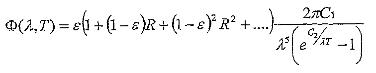
광학 프로브(20)로부터 얻어진 고온계 내의 잠재적인 대형 에러를 도입하는 요소는 기판(19)의 방사율이다. 플랭크의 법칙은 온도와 방사 사이의 관계를 정량화한다.The factor that introduces a potential large error in the pyrometer obtained from the

식 1에서, φ는 방사력이고, 고온계(20)에 의해 측정된 실제 양이며, C1 및 C2 는 상수이고, λ는 방사 파장이고(예를 들면, 상술된 실시예에서의 905 mm일 수 있는), T는 기판(19)의 온도이고, ε는 기판(19)의 방사율이다. 방사율이 알려진 경우, 플랭크의 법칙은 기판(19)의 온도를 매우 정밀하게 계산하기 위해 이용될 수 있다. 이러한 방사율이 알려지지 않은 경우, 정확한 온도 계산을 수행하는 것이 가능하지 않으며, 초래된 에러는 가정 방사율과 실제 방사율 사이의 차이에 따라 대형일 수 있다. 도 2는 가정된 방사율이 1.0으로 설정되는 경우 상이한 방사율의 기판(19)에 대해 발생될 수 있는 이론적인 온도 측정 에러의 크기를 보여준다. 예를 들면, 0.35의 방사율을 가지는 기판(19)이 1.0의 방사율을 가지는 것을 부정확하게 측정하는 경우, 800℃에서 형성되는 에러는 70℃에 근접하게 된다. 선택적인 실리콘 증착 분야에 대해, 넓은 범위의 방사율을 가지는 기판(19)이 처리될 것이 요구되고, 이러한 방사율이 미리 알려지지 않는 것이 예상될 수 있다.In
도 1b를 참조하여 설명하면, 하나의 실시예가 기판(19) 바로 위에 위치하는 높은 반사면(13)을 제공한다. 반사면(13)은 기판(19)에 의해 방사되는 광 방사선을 잡아서 이 광 방사선을 자체와 기판(19) 사이에서 전방 및 후방으로 반사하여, 방사율 강화 효과를 형성한다. 포함된 메카니즘은 도 3을 참조하여 설명될 수 있다. 반사면(13) 위에 배치되는 광학 프로브(20)는 기판(19)으로부터 도 3에서 Φ로 표시된 직접적인 방사 뿐만 아니라 두 개의 표면(13, 19) 사이의 다수의 반사를 수용하게 된다. 반사표면(13)을 이용하여 광학 프로브(20)에 도달하는 총 방사력은 Referring to FIG. 1B, one embodiment provides a high
여기서, R은 반사면(13)의 반사율(1.0에 근접한)이다. 이의 식은 아래와 같다.Here, R is the reflectance (close to 1.0) of the reflecting

여기서, here,

ε겉보기(apparent)가 ε 및 R의 소정의 실제값 그리고 특히 1.0에 근접한 R의 값에 대해 1.0이 되는 것이 용이하게 계산될 수 있다. 이는 기판(19)의 실제 방사율에 관계없이, 광학 프로브(또는 고온계)(20)가 1.0에 근접한 유효 방사율을 가진 타깃으로 간주된다는 것을 의미한다.It can be easily calculated that the epsilon apparent becomes 1.0 for a given actual value of epsilon and R and in particular for the value of R close to 1.0. This means that irrespective of the actual emissivity of the
따라서, 반사면(13)은 기판(19) 반사율에서의 변화에 대한 보상에 매우 효과적이다. 도 4는 반사율 효과에 의해 발생된 온도 에너지의 측정 에러를 보여준다. 도 1 및 도 5를 추가로 참조하면, 매우 낮은 방사율 상부면(약 0.35의 방사율을 가진 폴리실리콘 필름)을 가진 테스트 기판(100)이 열전쌍(101)으로 조립된다. 열전쌍(101)은 광학 프로브(20)와 동일한 반경에 위치하여 두 개의 기술에 의해 얻어진 온도 측정치가 비교된다. 도 4는 광학 프로브(20)에 의해 측정된 온도와 열전쌍(101)에 의해 측정된 온도 사이의 차이의 그래프이다. 도 4에 도시된 바와 같이, 방사율에 의한 에러는 최고 850℃ 온도에 대해 5℃ 보다 작다. 도 2를 참조하면, 반사면(13)에 의해 발생되는 강화되는 유효 방사율 없이 0.35의 방사율을 가진 기판(19)에 대해 측정 에러가 대신 850℃의 온도에서 70℃를 초과하게 된다. 따라서 반사면(13)은 90% 이상만큼 방사율 유도 에러를 감소시킨다.Thus, the reflecting
방사 가열되는 처리 챔버에 대해 고온계를 이용할 때 발생되는 또 다른 문제점은 미로 방사선이다. 도 1을 참조하면, 기판(19)은 방사선 가열 시스템을 이용하여 가열될 수 있다. 방사 가열 시스템은 기판(19)을 가열하기 위하여 하나 또는 그 이상의 램프(38)를 이용한다. 결론적으로, 챔버(15)는 광으로 투광된다. 이러한 배열체에서의 하나의 문제점은 방사 가열 시스템에 의해 생성된 광이 기판(19)에 의해 방사된 광과 거의 구별할 수 없다는 것이다. 이는 고온계(20)가 이러한 성분 둘다, 기판(19)으로부터의 방사 및 가열 시스템으로부터의 방사선을 수집하게 되고 이러한 방사선 모두 기판(19)에 의해 생산된 것으로 이해된다는 것을 의미한다. 이는 크기가 수백 썹씨 온도에 용이하게 도달할 수 있는 직접적인 측정 에러를 보여준다. 예를 들면, 도 6은 미로 방사선 피쳐(feature)가 거의 또는 전혀 이용되지 않을 때 고온계 온도 판독의 비교 데이터를 제공하는 그래프이다. 도 6에서, 데이터는 챔버가 가열되는 시간을 가지지 않을 정도로 충분히 빠른 속도로 단계에서 방사 가열 시스템의 램프 파워를 증가시킴으로써 얻을 수 있다. 열전쌍으로 측정된 실제 기판 온도는 전체 테스트 동안 결코 140℃를 초과하지 않는다. 고온계에 의해 측정된 바와 같은 그래프에 도시된 겉보기 온도에서의 모든 점프가 미로 방사선에 의해 발생된 직접적인 측정 에러이다. 도 6에 도시된 바와 같이, 이러한 에러는 300℃를 초과한다.Another problem that arises when using a pyrometer for a process chamber that is radiation heated is maze radiation. Referring to FIG. 1, the
본 발명의 하나의 양태는 미로 방사선과 관련된 문제점을 최소화하기 위해 시스템 부품 및 피쳐를 제공하는 것이고, 이러한 양태의 일 실시예는 도 7 및 도 8에 도시된다. 석영으로 제조될 수 있는 측벽(201)에 의해 둘러싸이는 처리 챔버(200)를 포함하는 시스템이 도시된다. 도 1에 대해 상술된 바와 같이, 시스템 내에 회전가능하게 배치되는 것은 필름 형성 공정 동안 기판(204)을 홀딩하기 위해 이용되는 기판 지지부(202)이다. 필름 형성 공정을 위해 요구되는 공정 가열 모두 기판 지지부(202) 아래 배치되어 기판(204) 아래 배치되는 방사 가열 시스템에 의해 제공된다. 필름 형성 시스템은 두 개의 영역, 즉 기판(204)의 상부 영역(206), 및 기판 지지부(202) 아래인 하부 영역(207)으로 분리되는 것으로 생각될 수 있다. 방사 가열 시스템이 하부 영역에 배타적으로 위치될 수 있기 때문에, 방사 가열 시스템으로부터의 광이 상부 영역(204)으로 유입되는 것을 방지하는 것이 바람직하며, 이는 고온계(또는 광학 프로브)가 기판(204)의 온도를 측정하기 위해 위치하기 때문이다.One aspect of the present invention is to provide system components and features to minimize the problems associated with maze radiation, one embodiment of which is shown in FIGS. 7 and 8. A system is shown that includes a
측벽(201)의 적어도 일 부분 주위에 주변 부재(205)가 배치된다. 레지(ledge) 및 포켓은 측벽(201) 및 주변 부재(205)에 설계될 수 있어 상기 두 개 부재가 서로에 대해 운동하는 것을 방지하도록 하고, 주변 부재(205)의 외측 주변 에지는 측벽(201)의 지지 에지(203)와 접촉한다. 주변 부재(205)는 예를 들면, 예비 가열 링일 수 있다. 주변 부재(205)는 흑연으로 제조될 수 있어, 광이 측벽(201)을 통하여 처리 챔버 내로 전달되는 것을 방지하며, 처리 챔버는 석영으로 제조될 수 있어 따라서 투명성 또는 반투명성일 수 있다. 주변 부재(205)는 처리 챔버(200) 내로 연장하는 내측 단부(208)를 포함한다. 이러한 내측 단부(208)는 기판 지지부(202)의 외측 단부(209)와 중첩된다. 따라서, 주변 부재(205) 및 기판 지지부(202)는 각각 중첩되는 내측 및 외측 에지 부분(208, 209)이다. 갭(210)은 회전하는 기판 지지부(202)와 고정 주변 부재(205) 사이에 제공될 수 있다. 중첩되는 단부(208, 209)를 분리하는 갭(210)의 폭은 가능한 작게 제조되어 갭(210)을 통과하는 칩의 양이 최소가 되도록 유지하며, 일 실시예에서는 0.075 인치의 폭을 가진다. 한 세트의 중첩하는 표면(208, 209)을 제공함으로써, 하부 영역(207)으로부터 돌출되는 대부분의 광은 상부 영역(206) 내로 유입되는 것이 차단된다. 중첩하는 표면(208, 209)은 기판 지지부(202)의 외측 주변 에지 및 주변 부재(205)의 내측 주변 에지에 스텝형 피쳐(stepped feature)를 포함할 수 있다. 기판 지지부(202) 및 주변 부재(205)의 스텝형 피쳐는 상보적인 것으로 도시되어 있다. 기판 지지부(202)의 외측 주변 에지(209)와 주변 부재(205)의 내부 주변 부재(208) 사이의 상보적인 스텝형 설계를 제공함으로써, 내측 주변 에지(208)의 상부면은 기판 지지부(202)의 상부면 위로 상승하지 않는다는 것에 주목하여야 한다.
하부 영역(207)으로부터의 광이 갭(210)을 경유하여 상부 영역(206) 내로 누출되는 것을 추가로 방지하기 위하여, 중첩 표면(208, 209)은 광을 확산시키고 흡수하도록 설계되는 광학적으로 거친 마무리를 제공할 수 있다. 예를 들면, 기판 지지부(202)의 외측 단부(209)의 상부면은 일련의 좁은 그루브(211)를 제공함으로써 기계가공될 수 있다. 주변 부재(205)의 내측 단부(208)의 바닥면은 유사하게 그루브형 표면이 제공될 수 있다. 비록 그루브가 이용되었지만, 광을 흡수하는 소정의 적절한 표면이 다른 타입의 각도가 형성된 표면, 또는 방사 가열 시스템에 의해 방사되는 방사선을 흡수하도록 설계되는 광학 필름과 같은, 중첩 표면(208, 209)에 이용될 수 있는 것으로 이해되어야 한다.To further prevent light from the
미로 방사선을 추가로 차단하기 위하여, 도 7 및 도 8에 도시된 실시예는 상부 주변 부재, 또는 광 차폐부(212)를 추가로 제공한다. 상부 광 차폐부((212)는 흑연으로 제조될 수 있어, 주변 부재(205) 및 서셉터(202)의 중첩 단부(208, 209) 위에 배치된다. 상부 광 차폐부(212)는 상부 측벽(213)에 배치되거나 인접하게 배치된다. 상부 측벽(213)은 석영으로 제조된다. 레지 및 포켓은 상부 측벽(213) 및 광 차폐부(212)에 설계될 수 있어 이러한 두 개의 부재가 서로에 대해 운동하는 것을 방지하도록 한다. 갭(215)은 주변 부재(205) 및 기판 지지부(202)의 상부면들로부터 상부 광 차폐부(212)의 하부면(214)을 분리할 수 있다. 상부 광 차폐부(212)의 하부면(214)은 유사하게 갭(210)으로부터 나오는 광을 흡수하도록 일련의 미세한 그루브 또는 광학 활성 필름과 같은 광학적으로 세공되지 않거나 흡수성 표면을 제공할 수 있다. 상부 광 차폐부(212)는 측벽(201, 213)의 전체 매개변수를 따를 수 있다. 비록 불연속 요소로서 설명되었지만, 상부 측벽(213) 및 하부 측벽(201)은 주변 부재(205)를 수용하도록 적절한 그루브 등으로 제조되는, 일체형 요소로 제조될 수 있다.To further block the maze radiation, the embodiment shown in FIGS. 7 and 8 further provides an upper peripheral member, or
서셉터가 기판 지지부(202)를 위해 이용되는 경우와 같이, 기판 지지부(202)가 기판(204)의 바닥면을 완전히 커버하는 것이 필요하지 않다. 대신, 에지 링은 기판 지지부(202)를 위해 이용될 수 있으며, 이 경우 기판 지지부(202)는 단지 기판(204)의 에지에 의해 기판(204)을 지지한다. 이 경우, 가열 시스템은 기판(204)의 바닥을 직접 가열한다. 이 같은 구성은 시스템의 중량을 감소시켜 온도를 매우 신속하게 상승시킨다는 점에서 유용할 수 있다.As is the case when the susceptor is used for the
도 9는 석영 측벽(302)에 의해 경계가 형성되는 처리 챔버(301), 및 상부 커버(303)를 포함하는, 또 다른 막 형성 시스템(300)이 도시된다. 기판 지지 샤프트(304)는 처리 챔버(301) 내에 회전가능하게 배치되고, 기판(306)을 홀딩하는 서셉터(305)를 포함한다. 서셉터(305)는 흑연 또는 고체형 실리콘 카바이드와 같은 가볍고, 균일한 열 전도성 재료(100 와트(미터 ℃) 또는 그 이상)로 제조되어, 기판(306)의 바닥면을 완전히 덮어서, 전도 및 복사에 의해 기판(306)을 가열하도록 설계된다. 상부 커버(303)는 석영 내부 층(308)과 강철 외부 층(309) 사이에 끼워지는 반사면(307)을 포함한다. 반사면(307)은 기판(306)으로부터 역으로 기판(306)의 상부면을 향하여 방출되는 방사선을 반사하여 기판(306)의 유효 방사율을 증가시키도록 한다.9 shows another
방사율 강화 효과로, 기판(306)은 기판(306)의 표면 상의 방사율 값 또는 패턴과 관계없이 균일한 등온 상태에 도달할 때까지 반사면(307)이 에너지를 기판(306)으로 역으로 일정하게 반사한다. 기판(306)의 온도의 고온계 측정을 위해 제공하기 위하여, 다수의 광학 프로브(310)는 기판(306)으로부터 나오는 광을 샘플링하며, 각각의 광학 프로브(310)는 기판(306)을 넘어 연장하지 않는 각각의 시야(311)를 가진다. 각각의 표면(307) 내의 개구(312)는 광학 프로브(310)로 각각의 시야(311)를 제공할 수 있다.With an emissivity enhancing effect, the
필름 형성 시스템(300)은 기판 지지부(305) 아래 배치되는 가열 시스템(313)을 포함한다. 가열 시스템(313)은 하나 또는 그 이상의 램프(314)를 포함하며, 이 램프는 기판 지지부(305)의 바닥부를 가열하기 위하여 챔버(301) 내로 광을 방사한다. 모든 공정 가열은 가열 시스템(313)에 의해 제공된다. 램프로부터의 광이 광학 프로브(310)에 도달하는 것을 방지하기 위하여, 시스템(300)은 서셉터(305)와 중복되는 예비 가열 링일 수 있는 흑연 주변 부재(315)를 더 포함한다. 따라서, 상기 실시예에서 설명된 바와 같이, 서셉터(305)와 주변 부재(315) 사이에 중첩 영역(316)이 존재한다. 이러한 중첩 영역(316) 내의 표면은 미세한 그루브 또는 광학의 얇은 필름을 구비하는 것과 같이 광학적으로 세공되지 않거나 흡수성이 될 수 있어, 주변 부재(315)로부터 서셉터(304)를 분리하는 갭을 통하여 산란되는 광을 더 흡수하도록 한다. 흑연 상부 주변 부재 또는 광 차폐부(317)는 또한 중복의 영역(316) 위에 배치될 수 있어 램프(314)로부터 산란되는 광을 추가로 차단하도록 한다. 광 차폐부(317)는 석영 상부 측벽(318)에 의해 지지될 수 있다.The
필름 형성 시스템(300)은 통상적으로 기판(306)의 패턴 로딩 및 방사율 변화의 결과인 필름 형성 공정에서의 결함을 방지하도록 설계된다. 서셉터(305)는 가열 시스템(313)을 위한 일정 흡수율 타깃을 제공한다. 따라서 가열 시스템(313)은 서셉터(305)를 균일하게 가열하며, 이어서 기판을 균일 전도 방식으로 가열하며, 반사면(307)은 패턴 로딩 및 방사율 효과를 회피하도록 기판(306)에 걸친 등온 상태를 추가로 보장한다. 반사면(307)은 두 개의 구별되는 특징을 제공한다: 즉 1) 기판(306)의 전체 방사율과 관계없이, 프로브(310)가 기판(306)의 온도를 정확히 측정하고, 그리고 2) 기판(306)의 방사율에서의 국부적인, 나노 스케일, 변화에 의해 발생되는 패턴 로딩 효과를 감소시키도록 한다.The
도 10은 필름 형성 시스템(300)을 위한 열전쌍 온도 데이터에 대한 고온계 온도 데이터의 실험적인 결과를 보여주는 그래프이다. 광학 프로브(310)에 의해 측정된 고온계 온도를 명확히 하기 위하여, 도 5에 도시된 것과 유사한 특별한 웨이퍼가 상부면에 용접되는 4개의 열전쌍을 가지는 것을 이용하였다. 열전쌍은 광학 프로브(310) 아래 직접 위치하여 광학 프로브(310)의 고온계 판독이 직접 비교 되도록 한다. 고 방사율 필름(약 0.95의)은 열전쌍을 부착하기 전에 웨이퍼의 표면 상에서 성장되었다. 이에 의해, 광학 프로브(310)의 정밀도 및 반복가능성은 임의의 열적 사이클을 통하여 웨이퍼를 가열하고 광학 프로브(310)에 의해 얻어진 것과 열전쌍 판독치를 비교함으로써 테스트되었다. 기판의 중앙 근처에 위치하는 열전쌍 및 광학 프로브를 그래프로 도시하는 도 10에 도시된 바와 같이, 시스템(300)은 광학 프로브(310)를 경유하여 고온계를 통하여 측정된 바와 같이 열전쌍 대 온도에 의해 측정된 바와 같은 온도들 사이의 긴밀한 관계를 제공한다.FIG. 10 is a graph showing experimental results of pyrometer temperature data versus thermocouple temperature data for
도 11은 이러한 테스트 동안 얻어지는 실제 챔버(301) 온도의 함수로서 모든 광학 프로브(310)에 걸쳐 계산된 평균 측정 에러의 윤곽(summary)을 보여준다. 도시된 바와 같이, 관심있는 온도 범위(> 550℃)에 대해, 미광에 의한 에러는 2℃ 정도(order) 상에 있다.FIG. 11 shows a summary of the mean measurement error calculated across all
고온계 측정을 위한 방사율 효과 정정을 위해 추가로 제공되는 필름 형성 시스템(400)의 또 다른 실시예가 도 12에 도시된다. 필름 형성 시스템(400)은 도 9의 시스템(300)과 유사하지만, 시스템(400)은 기판(420)의 실제 방사율을 측정하기 위한 이미소미터(410)를 추가로 포함한다. 이미소미터(410)의 작동의 원리는 챔버(402) 내에 광학 프로브(403)를 위치설정하는 단계를 포함하지만, 광학 프로브(403)에 대해 반사면(401)에 의해 제공되는 강화되고 유효 방사율이 감소 또는 제거된다. 광학 프로브(403)는 어떠한 반사 방사선도 없이, 기판(420)으로부터의 직접적인 방사선만을 보여준다. 즉, 광학 프로브(403)가 측정한 방사 파워는,Another embodiment of a

반사면(401)의 완전히 강화된 방사율 효과를 경험하는 이웃하는 광학 프로브(404)에 의해 측정된 온도에 광학 프로브(403)에 의해 측정된 온도를 비교함으로써, 기판(420)의 실제 방사율을 계산하는 것이 가능하다. 예를 드면, 기판(420)의 방사율이 아래와 같이 계산될 수 있다.Compute the actual emissivity of the

Tmeas는 측정된 웨이퍼 온도이고, 델타(delta)는 온도 프로브(404) 및 이미소미터 프로브(403)에 의해 측정된 온도에서의 차이이고 R3는 반사면(401)의 반사율이고 RE는 이미소미터(410) 주위의 공동의 반사율이다. 다른 상수가 식 1로서 주어진다. 이와 달리, 0.3 내지 약 0.95의 공지된 방사율의 수 개의 기판(420)는 챔버(402) 내에서 작동될 수 있으며 이미소미터(410) 및 정규 고온계(404) 사이의 온도 델타는 측정 곡선을 형성하기 위하여 측정될 수 있다. 이러한 측정 곡선은 지수 함수와 맞추어질 수 있어 후속적으로 공지되지 않은 기판(420)의 방사율을 결정하기 위하여 이용된다. 방사율 값은 이어서 고온계 광학 프로브(405)에 의해 보고된 온도에 대한 정정을 수행하기 위하여 이용된다.Tmeas is the measured wafer temperature, delta is the difference in temperature measured by the
도 13은 이미소미터(410)의 일 실시예를 도시한다. 광학 프로브(403)는 상대적인 큰 직경 홀(406)이 드릴링 또는 에칭되는 반사면(401)의 영역 내에 위치된다. 홀(406)의 직경은 기판(420)에 대한 거리 및 광학 프로브(403)의 시야와 관련될 수 있다. 광학 프로브(403)는 반사면(401)으로부터 반사되지 않으면서 기판(420)으로부터 직접 나오는 광을 수집하여, 광학 프로브(403)가 반사면(401)에 의해 제공되는 방사율 강화 없이 수용되는 것이 바람직하다. 따라서, 홀(406)의 직경이 가능한 넓게 되는 것이 바람직하다. 그러나, 기판(420)이 거의 모든 각도에서 방사선을 방출하기 때문에, 홀(406)이 매우 크게 제조되지 않으면, 광학 프로브(403)는 거의 항상 소정의 방사율 강화 방사선을 수집한다. 매우 큰 홀(406)을 제조하는 것은 바람직하지 않을 수 있으며, 이는 기판(420) 상에 냉점을 형성하는 경향이 있기 때문이다. 기판(420)이 회전할 수 있기 때문에, 이러한 냉점은 기판(420) 상에 냉각 링을 형성하게 된다. 홀(406)의 직경을 광학 프로브(403)의 기판(420)의 표면 상의 시야와 동일한 크기로 제조함으로써 적절하게 타협될 수 있다. 일 실시예에서, 홀(406)의 직경이 0.5 내지 2인치의 범위일 수 있다. 일 실시예에서, 직경은 약 0.75 인치일 수 있다. 일반적으로, 삼각법이 이용될 수 있으며, 직경은 광학 프로브(403)와 기판(420)으로부터의 거리 및 광학 프로브(403)의 조망의 각도의 함수일 수 있다. 홀(406)의 폭은 효과적으로 프로브(403)에 도달하는 방사선에 대해 반사면(401)의 방사율 강화 효과를 효과적으로 제거한다. 반사면(401) 내의 대형 홀(406)이 기판(420)의 온도에 대한 역효과를 가지는 것을 방지하기 위하여, 고온 미러(407)가 구멍(406)을 덮기 위하여 위치설정된다. 고온 미러(407)는 광을 기판(420)으로 역으로 축선을 벗어나서 반사하도록 설계되며, 이는 홀(406)을 통한 열 손실 량을 최소화한다. 이와 같은 고온 미러가, 예를 들면, 세키덴코(Sekidenko)로부터 얻어질 수 있다. 고온 미러(407) 때문에, 프로브(403) 아래로 직접 방사되는 방사선만이 이미소미터(410)에 도달한다. 이러한 방사선은 반사면(401)에 의해 강화되지 않으며, 이어서 정규의 고온계 탐침(404, 405)과 비교될 수 있어, 상술된 바와 같이, 기판(420)의 방사율을 계산하도록 한다. 기판(420)의 방사율이 알려지면, 기판(420)의 온도는 식 1 및 광학 프로브(404, 405)에 의해 감지되는 방사 파워를 이용하여 정밀하게 결정될 수 있다.13 illustrates one embodiment of an
또한, 각각 기판의 시야를 구비하는 다중 이미소미터를 이용하여 대응하는 다수의 영역에 걸쳐 기판의 방사율을 결정하도록 하는 것이 가능하다. 상기 영역에 대해 이미소미터에 의해 측정된 바와 같은 하나의 영역 내의 기판의 방사율은 이어서 영역을 둘러싸는 시야를 구비하는 대응하는 고온계에 대한 상기 영역의 온도를 정밀하게 계산하기 위하여 이용될 수 있다. 이러한 방식으로, 기판에 걸친 온도 분포는 더욱 정밀하게 측정될 수 있어, 더욱 정밀하게 제어될 수 있다.In addition, it is possible to determine the emissivity of a substrate over a corresponding plurality of regions using multiple imagers each having a field of view of the substrate. The emissivity of the substrate in one region as measured by the imager for that region can then be used to precisely calculate the temperature of the region for the corresponding pyrometer having a field of view surrounding the region. In this way, the temperature distribution across the substrate can be measured more precisely, and thus more precisely controlled.
또 다른 실시예에 따라, 에너지의 조정가능한 소스가 필름 형성 챔버 내에서 온도를 제어하기 위해 제공된다. 도 14를 참조하면, 시스템(500)은 4개의 존 방사가열 시스템(510)을 포함하며, 각각의 존(501)은 고온계 광학 프로브(502)의 대응하는 방사형 분포로부터 수용되는 온도 피드백을 기초로하여 독립적으로 조정될 수 있다. 방사 가열 시스템(510)은 서셉터(505) 아래 배치되고, 다수의 램프(503) 및 반사기(504)를 포함한다. 램프(503) 및 반사기(504)의 배향 및 각도에 대한 조정은 독립적으로 조정가능한 가열 존(501)을 형성한다.According to another embodiment, an adjustable source of energy is provided for controlling the temperature in the film forming chamber. Referring to FIG. 14,
가열 영역(501)은 서셉터(505)의 바닥면을 가로질러 균일하게 되도록 조정될 수 있는 가열 패턴을 생산하기 위하여 조합된다. 서셉터(505)의 바닥면은 광학 필름, 그루브, 등을 이용하는 것과 같이, 램프(503)에 의해 방사되는 방사선을 최대로 흡수하도록 설계될 수 있다. 가열 시스템(510)에 의해 발생되는 가열 패턴의 그래프는 도 15에 제시되며, 독립적으로 턴온될 때 각각의 개별 가열 존(501)에 대해 서셉터(505)에 걸쳐 측정되는 가열 분포를 보여준다. 각각의 가열 존(501)은 서셉터(505) 상의 특정 반경에서 및 이에 따라 기판(507) 상의 특정 반경에서(각각의 존(501)의 가열 분포는 서셉터(505)의 회전 중앙에 대해 대칭이다) 기판(507)을 가열하며, 모든 가열 존(501)은 균일한 가열 분포를 형성하기에만 충분하게 중복된다. 도 15에 표시된 가열 패턴의 가열 존(501)이 1σ에 대해 1℃ 보다 더 우수한 기판(507)에 걸쳐 온도 분포를 형성하기 위하여 중첩된다. 더욱이, 상술된 바와 같이, 배타적으로 바닥으로부터 기판(507)을 가열함으로써 방사율 및 패턴 로드 효과를 감소시킨다.The
상술된 것은 본 발명의 실시예들에 관한 것인 반면, 본 발명의 다른 및 추가 실시예는 본 발명의 기본 범위로부터 이탈하지 않고 고안될 수 있으며, 본 발명의 범위는 후술되는 청구범위에 의해 결정된다.While the foregoing is directed to embodiments of the invention, other and further embodiments of the invention may be devised without departing from the basic scope thereof, and the scope thereof is determined by the claims that follow. do.
Claims (20)
Applications Claiming Priority (3)
| Application Number | Priority Date | Filing Date | Title |
|---|---|---|---|
| US11/242,299 US8372203B2 (en) | 2005-09-30 | 2005-09-30 | Apparatus temperature control and pattern compensation |
| US11/242,299 | 2005-09-30 | ||
| PCT/US2006/035263 WO2007040916A2 (en) | 2005-09-30 | 2006-09-11 | Apparatus temperature control and pattern compensation |
Publications (2)
| Publication Number | Publication Date |
|---|---|
| KR20080055973A KR20080055973A (en) | 2008-06-19 |
| KR101047088B1 true KR101047088B1 (en) | 2011-07-06 |
Family
ID=37900710
Family Applications (1)
| Application Number | Title | Priority Date | Filing Date |
|---|---|---|---|
| KR1020087010503A Active KR101047088B1 (en) | 2005-09-30 | 2006-09-11 | Device temperature control and pattern compensation device method |
Country Status (5)
| Country | Link |
|---|---|
| US (1) | US8372203B2 (en) |
| JP (1) | JP5205268B2 (en) |
| KR (1) | KR101047088B1 (en) |
| TW (1) | TWI367956B (en) |
| WO (1) | WO2007040916A2 (en) |
Families Citing this family (323)
| Publication number | Priority date | Publication date | Assignee | Title |
|---|---|---|---|---|
| US7691204B2 (en) * | 2005-09-30 | 2010-04-06 | Applied Materials, Inc. | Film formation apparatus and methods including temperature and emissivity/pattern compensation |
| US20090194024A1 (en) * | 2008-01-31 | 2009-08-06 | Applied Materials, Inc. | Cvd apparatus |
| KR101011689B1 (en) * | 2008-03-14 | 2011-01-31 | (주)테크윙 | Temperature control unit for electronic component inspection support device |
| US8333083B2 (en) * | 2008-03-14 | 2012-12-18 | Techwing Co., Ltd. | System to support testing of electronic devices, temperature control unit for the system, and method for controlling internal temperature of chamber of the system |
| EP2271587A1 (en) * | 2008-03-26 | 2011-01-12 | GT Solar Incorporated | Gold-coated polysilicon reactor system and method |
| EP2409319A4 (en) * | 2009-03-16 | 2013-07-24 | Alta Devices Inc | HEATING LAMP SYSTEM AND METHODS THEREOF |
| US9394608B2 (en) | 2009-04-06 | 2016-07-19 | Asm America, Inc. | Semiconductor processing reactor and components thereof |
| US8802201B2 (en) | 2009-08-14 | 2014-08-12 | Asm America, Inc. | Systems and methods for thin-film deposition of metal oxides using excited nitrogen-oxygen species |
| US20120148760A1 (en) * | 2010-12-08 | 2012-06-14 | Glen Eric Egami | Induction Heating for Substrate Processing |
| JP5819633B2 (en) * | 2011-05-13 | 2015-11-24 | 株式会社Screenホールディングス | Heat treatment apparatus and heat treatment method |
| US20130023129A1 (en) | 2011-07-20 | 2013-01-24 | Asm America, Inc. | Pressure transmitter for a semiconductor processing environment |
| DE102011083245B4 (en) * | 2011-09-22 | 2019-04-25 | Siltronic Ag | Method and device for depositing an epitaxial layer of silicon on a semiconductor wafer of monocrystalline silicon by vapor deposition in a process chamber |
| US9017481B1 (en) | 2011-10-28 | 2015-04-28 | Asm America, Inc. | Process feed management for semiconductor substrate processing |
| US10714315B2 (en) | 2012-10-12 | 2020-07-14 | Asm Ip Holdings B.V. | Semiconductor reaction chamber showerhead |
| SG10201708105UA (en) * | 2013-01-16 | 2017-11-29 | Applied Materials Inc | Quartz upper and lower domes |
| US20160376700A1 (en) | 2013-02-01 | 2016-12-29 | Asm Ip Holding B.V. | System for treatment of deposition reactor |
| US11015244B2 (en) | 2013-12-30 | 2021-05-25 | Advanced Material Solutions, Llc | Radiation shielding for a CVD reactor |
| US11015245B2 (en) | 2014-03-19 | 2021-05-25 | Asm Ip Holding B.V. | Gas-phase reactor and system having exhaust plenum and components thereof |
| US10858737B2 (en) | 2014-07-28 | 2020-12-08 | Asm Ip Holding B.V. | Showerhead assembly and components thereof |
| US9890456B2 (en) | 2014-08-21 | 2018-02-13 | Asm Ip Holding B.V. | Method and system for in situ formation of gas-phase compounds |
| US10941490B2 (en) | 2014-10-07 | 2021-03-09 | Asm Ip Holding B.V. | Multiple temperature range susceptor, assembly, reactor and system including the susceptor, and methods of using the same |
| US10276355B2 (en) | 2015-03-12 | 2019-04-30 | Asm Ip Holding B.V. | Multi-zone reactor, system including the reactor, and method of using the same |
| US20160282886A1 (en) * | 2015-03-27 | 2016-09-29 | Applied Materials, Inc. | Upper dome temperature closed loop control |
| US9879358B2 (en) * | 2015-05-27 | 2018-01-30 | Applied Materials, Inc. | Heat shield ring for high growth rate EPI chamber |
| US10458018B2 (en) | 2015-06-26 | 2019-10-29 | Asm Ip Holding B.V. | Structures including metal carbide material, devices including the structures, and methods of forming same |
| US10211308B2 (en) | 2015-10-21 | 2019-02-19 | Asm Ip Holding B.V. | NbMC layers |
| US11139308B2 (en) | 2015-12-29 | 2021-10-05 | Asm Ip Holding B.V. | Atomic layer deposition of III-V compounds to form V-NAND devices |
| US10529554B2 (en) | 2016-02-19 | 2020-01-07 | Asm Ip Holding B.V. | Method for forming silicon nitride film selectively on sidewalls or flat surfaces of trenches |
| US10343920B2 (en) | 2016-03-18 | 2019-07-09 | Asm Ip Holding B.V. | Aligned carbon nanotubes |
| US10865475B2 (en) | 2016-04-21 | 2020-12-15 | Asm Ip Holding B.V. | Deposition of metal borides and silicides |
| US10190213B2 (en) | 2016-04-21 | 2019-01-29 | Asm Ip Holding B.V. | Deposition of metal borides |
| US10367080B2 (en) | 2016-05-02 | 2019-07-30 | Asm Ip Holding B.V. | Method of forming a germanium oxynitride film |
| US11453943B2 (en) | 2016-05-25 | 2022-09-27 | Asm Ip Holding B.V. | Method for forming carbon-containing silicon/metal oxide or nitride film by ALD using silicon precursor and hydrocarbon precursor |
| KR102113453B1 (en) * | 2016-06-03 | 2020-05-21 | 어플라이드 머티어리얼스, 인코포레이티드 | Substrate distance monitoring |
| US10612137B2 (en) | 2016-07-08 | 2020-04-07 | Asm Ip Holdings B.V. | Organic reactants for atomic layer deposition |
| US9859151B1 (en) | 2016-07-08 | 2018-01-02 | Asm Ip Holding B.V. | Selective film deposition method to form air gaps |
| US9812320B1 (en) | 2016-07-28 | 2017-11-07 | Asm Ip Holding B.V. | Method and apparatus for filling a gap |
| US9887082B1 (en) | 2016-07-28 | 2018-02-06 | Asm Ip Holding B.V. | Method and apparatus for filling a gap |
| KR102532607B1 (en) | 2016-07-28 | 2023-05-15 | 에이에스엠 아이피 홀딩 비.브이. | Substrate processing apparatus and method of operating the same |
| US10643826B2 (en) | 2016-10-26 | 2020-05-05 | Asm Ip Holdings B.V. | Methods for thermally calibrating reaction chambers |
| US11532757B2 (en) | 2016-10-27 | 2022-12-20 | Asm Ip Holding B.V. | Deposition of charge trapping layers |
| US10229833B2 (en) | 2016-11-01 | 2019-03-12 | Asm Ip Holding B.V. | Methods for forming a transition metal nitride film on a substrate by atomic layer deposition and related semiconductor device structures |
| US10714350B2 (en) | 2016-11-01 | 2020-07-14 | ASM IP Holdings, B.V. | Methods for forming a transition metal niobium nitride film on a substrate by atomic layer deposition and related semiconductor device structures |
| KR102546317B1 (en) | 2016-11-15 | 2023-06-21 | 에이에스엠 아이피 홀딩 비.브이. | Gas supply unit and substrate processing apparatus including the same |
| KR102762543B1 (en) | 2016-12-14 | 2025-02-05 | 에이에스엠 아이피 홀딩 비.브이. | Substrate processing apparatus |
| US11447861B2 (en) | 2016-12-15 | 2022-09-20 | Asm Ip Holding B.V. | Sequential infiltration synthesis apparatus and a method of forming a patterned structure |
| US11581186B2 (en) | 2016-12-15 | 2023-02-14 | Asm Ip Holding B.V. | Sequential infiltration synthesis apparatus |
| KR102700194B1 (en) | 2016-12-19 | 2024-08-28 | 에이에스엠 아이피 홀딩 비.브이. | Substrate processing apparatus |
| US10269558B2 (en) | 2016-12-22 | 2019-04-23 | Asm Ip Holding B.V. | Method of forming a structure on a substrate |
| US10867788B2 (en) | 2016-12-28 | 2020-12-15 | Asm Ip Holding B.V. | Method of forming a structure on a substrate |
| US11390950B2 (en) * | 2017-01-10 | 2022-07-19 | Asm Ip Holding B.V. | Reactor system and method to reduce residue buildup during a film deposition process |
| US10468261B2 (en) | 2017-02-15 | 2019-11-05 | Asm Ip Holding B.V. | Methods for forming a metallic film on a substrate by cyclical deposition and related semiconductor device structures |
| US10529563B2 (en) | 2017-03-29 | 2020-01-07 | Asm Ip Holdings B.V. | Method for forming doped metal oxide films on a substrate by cyclical deposition and related semiconductor device structures |
| KR102457289B1 (en) | 2017-04-25 | 2022-10-21 | 에이에스엠 아이피 홀딩 비.브이. | Method for depositing a thin film and manufacturing a semiconductor device |
| US10892156B2 (en) | 2017-05-08 | 2021-01-12 | Asm Ip Holding B.V. | Methods for forming a silicon nitride film on a substrate and related semiconductor device structures |
| US10770286B2 (en) | 2017-05-08 | 2020-09-08 | Asm Ip Holdings B.V. | Methods for selectively forming a silicon nitride film on a substrate and related semiconductor device structures |
| US10886123B2 (en) | 2017-06-02 | 2021-01-05 | Asm Ip Holding B.V. | Methods for forming low temperature semiconductor layers and related semiconductor device structures |
| US12040200B2 (en) | 2017-06-20 | 2024-07-16 | Asm Ip Holding B.V. | Semiconductor processing apparatus and methods for calibrating a semiconductor processing apparatus |
| US11306395B2 (en) | 2017-06-28 | 2022-04-19 | Asm Ip Holding B.V. | Methods for depositing a transition metal nitride film on a substrate by atomic layer deposition and related deposition apparatus |
| KR20190009245A (en) | 2017-07-18 | 2019-01-28 | 에이에스엠 아이피 홀딩 비.브이. | Methods for forming a semiconductor device structure and related semiconductor device structures |
| US11018002B2 (en) | 2017-07-19 | 2021-05-25 | Asm Ip Holding B.V. | Method for selectively depositing a Group IV semiconductor and related semiconductor device structures |
| US10541333B2 (en) | 2017-07-19 | 2020-01-21 | Asm Ip Holding B.V. | Method for depositing a group IV semiconductor and related semiconductor device structures |
| US11374112B2 (en) | 2017-07-19 | 2022-06-28 | Asm Ip Holding B.V. | Method for depositing a group IV semiconductor and related semiconductor device structures |
| US10590535B2 (en) | 2017-07-26 | 2020-03-17 | Asm Ip Holdings B.V. | Chemical treatment, deposition and/or infiltration apparatus and method for using the same |
| TWI815813B (en) | 2017-08-04 | 2023-09-21 | 荷蘭商Asm智慧財產控股公司 | Showerhead assembly for distributing a gas within a reaction chamber |
| US10770336B2 (en) | 2017-08-08 | 2020-09-08 | Asm Ip Holding B.V. | Substrate lift mechanism and reactor including same |
| US10692741B2 (en) | 2017-08-08 | 2020-06-23 | Asm Ip Holdings B.V. | Radiation shield |
| US11139191B2 (en) | 2017-08-09 | 2021-10-05 | Asm Ip Holding B.V. | Storage apparatus for storing cassettes for substrates and processing apparatus equipped therewith |
| US11769682B2 (en) | 2017-08-09 | 2023-09-26 | Asm Ip Holding B.V. | Storage apparatus for storing cassettes for substrates and processing apparatus equipped therewith |
| US11830730B2 (en) | 2017-08-29 | 2023-11-28 | Asm Ip Holding B.V. | Layer forming method and apparatus |
| KR102491945B1 (en) | 2017-08-30 | 2023-01-26 | 에이에스엠 아이피 홀딩 비.브이. | Substrate processing apparatus |
| US11295980B2 (en) | 2017-08-30 | 2022-04-05 | Asm Ip Holding B.V. | Methods for depositing a molybdenum metal film over a dielectric surface of a substrate by a cyclical deposition process and related semiconductor device structures |
| US11056344B2 (en) | 2017-08-30 | 2021-07-06 | Asm Ip Holding B.V. | Layer forming method |
| KR102401446B1 (en) | 2017-08-31 | 2022-05-24 | 에이에스엠 아이피 홀딩 비.브이. | Substrate processing apparatus |
| KR102630301B1 (en) | 2017-09-21 | 2024-01-29 | 에이에스엠 아이피 홀딩 비.브이. | Method of sequential infiltration synthesis treatment of infiltrateable material and structures and devices formed using same |
| US10844484B2 (en) | 2017-09-22 | 2020-11-24 | Asm Ip Holding B.V. | Apparatus for dispensing a vapor phase reactant to a reaction chamber and related methods |
| US10658205B2 (en) | 2017-09-28 | 2020-05-19 | Asm Ip Holdings B.V. | Chemical dispensing apparatus and methods for dispensing a chemical to a reaction chamber |
| US10403504B2 (en) | 2017-10-05 | 2019-09-03 | Asm Ip Holding B.V. | Method for selectively depositing a metallic film on a substrate |
| US10923344B2 (en) | 2017-10-30 | 2021-02-16 | Asm Ip Holding B.V. | Methods for forming a semiconductor structure and related semiconductor structures |
| US10910262B2 (en) | 2017-11-16 | 2021-02-02 | Asm Ip Holding B.V. | Method of selectively depositing a capping layer structure on a semiconductor device structure |
| US11022879B2 (en) | 2017-11-24 | 2021-06-01 | Asm Ip Holding B.V. | Method of forming an enhanced unexposed photoresist layer |
| KR102597978B1 (en) | 2017-11-27 | 2023-11-06 | 에이에스엠 아이피 홀딩 비.브이. | Storage device for storing wafer cassettes for use with batch furnaces |
| CN111344522B (en) | 2017-11-27 | 2022-04-12 | 阿斯莫Ip控股公司 | Units including clean mini environments |
| US10872771B2 (en) | 2018-01-16 | 2020-12-22 | Asm Ip Holding B. V. | Method for depositing a material film on a substrate within a reaction chamber by a cyclical deposition process and related device structures |
| TWI799494B (en) | 2018-01-19 | 2023-04-21 | 荷蘭商Asm 智慧財產控股公司 | Deposition method |
| WO2019142055A2 (en) | 2018-01-19 | 2019-07-25 | Asm Ip Holding B.V. | Method for depositing a gap-fill layer by plasma-assisted deposition |
| US11018047B2 (en) | 2018-01-25 | 2021-05-25 | Asm Ip Holding B.V. | Hybrid lift pin |
| USD880437S1 (en) | 2018-02-01 | 2020-04-07 | Asm Ip Holding B.V. | Gas supply plate for semiconductor manufacturing apparatus |
| US11081345B2 (en) | 2018-02-06 | 2021-08-03 | Asm Ip Holding B.V. | Method of post-deposition treatment for silicon oxide film |
| US11685991B2 (en) | 2018-02-14 | 2023-06-27 | Asm Ip Holding B.V. | Method for depositing a ruthenium-containing film on a substrate by a cyclical deposition process |
| US10896820B2 (en) | 2018-02-14 | 2021-01-19 | Asm Ip Holding B.V. | Method for depositing a ruthenium-containing film on a substrate by a cyclical deposition process |
| US10731249B2 (en) | 2018-02-15 | 2020-08-04 | Asm Ip Holding B.V. | Method of forming a transition metal containing film on a substrate by a cyclical deposition process, a method for supplying a transition metal halide compound to a reaction chamber, and related vapor deposition apparatus |
| KR102636427B1 (en) | 2018-02-20 | 2024-02-13 | 에이에스엠 아이피 홀딩 비.브이. | Substrate processing method and apparatus |
| US10975470B2 (en) | 2018-02-23 | 2021-04-13 | Asm Ip Holding B.V. | Apparatus for detecting or monitoring for a chemical precursor in a high temperature environment |
| US11473195B2 (en) | 2018-03-01 | 2022-10-18 | Asm Ip Holding B.V. | Semiconductor processing apparatus and a method for processing a substrate |
| US11629406B2 (en) | 2018-03-09 | 2023-04-18 | Asm Ip Holding B.V. | Semiconductor processing apparatus comprising one or more pyrometers for measuring a temperature of a substrate during transfer of the substrate |
| US11114283B2 (en) | 2018-03-16 | 2021-09-07 | Asm Ip Holding B.V. | Reactor, system including the reactor, and methods of manufacturing and using same |
| KR102646467B1 (en) | 2018-03-27 | 2024-03-11 | 에이에스엠 아이피 홀딩 비.브이. | Method of forming an electrode on a substrate and a semiconductor device structure including an electrode |
| US11230766B2 (en) | 2018-03-29 | 2022-01-25 | Asm Ip Holding B.V. | Substrate processing apparatus and method |
| US11088002B2 (en) | 2018-03-29 | 2021-08-10 | Asm Ip Holding B.V. | Substrate rack and a substrate processing system and method |
| KR102501472B1 (en) | 2018-03-30 | 2023-02-20 | 에이에스엠 아이피 홀딩 비.브이. | Substrate processing method |
| KR102600229B1 (en) | 2018-04-09 | 2023-11-10 | 에이에스엠 아이피 홀딩 비.브이. | Substrate supporting device, substrate processing apparatus including the same and substrate processing method |
| TWI811348B (en) | 2018-05-08 | 2023-08-11 | 荷蘭商Asm 智慧財產控股公司 | Methods for depositing an oxide film on a substrate by a cyclical deposition process and related device structures |
| US12025484B2 (en) | 2018-05-08 | 2024-07-02 | Asm Ip Holding B.V. | Thin film forming method |
| US12272527B2 (en) | 2018-05-09 | 2025-04-08 | Asm Ip Holding B.V. | Apparatus for use with hydrogen radicals and method of using same |
| TWI816783B (en) | 2018-05-11 | 2023-10-01 | 荷蘭商Asm 智慧財產控股公司 | Methods for forming a doped metal carbide film on a substrate and related semiconductor device structures |
| KR102596988B1 (en) | 2018-05-28 | 2023-10-31 | 에이에스엠 아이피 홀딩 비.브이. | Method of processing a substrate and a device manufactured by the same |
| TWI840362B (en) | 2018-06-04 | 2024-05-01 | 荷蘭商Asm Ip私人控股有限公司 | Wafer handling chamber with moisture reduction |
| US11718913B2 (en) | 2018-06-04 | 2023-08-08 | Asm Ip Holding B.V. | Gas distribution system and reactor system including same |
| US11286562B2 (en) | 2018-06-08 | 2022-03-29 | Asm Ip Holding B.V. | Gas-phase chemical reactor and method of using same |
| US10797133B2 (en) | 2018-06-21 | 2020-10-06 | Asm Ip Holding B.V. | Method for depositing a phosphorus doped silicon arsenide film and related semiconductor device structures |
| KR102568797B1 (en) | 2018-06-21 | 2023-08-21 | 에이에스엠 아이피 홀딩 비.브이. | Substrate processing system |
| TWI815915B (en) | 2018-06-27 | 2023-09-21 | 荷蘭商Asm Ip私人控股有限公司 | Cyclic deposition methods for forming metal-containing material and films and structures including the metal-containing material |
| KR102854019B1 (en) | 2018-06-27 | 2025-09-02 | 에이에스엠 아이피 홀딩 비.브이. | Periodic deposition method for forming a metal-containing material and films and structures comprising the metal-containing material |
| KR102686758B1 (en) | 2018-06-29 | 2024-07-18 | 에이에스엠 아이피 홀딩 비.브이. | Method for depositing a thin film and manufacturing a semiconductor device |
| US10612136B2 (en) | 2018-06-29 | 2020-04-07 | ASM IP Holding, B.V. | Temperature-controlled flange and reactor system including same |
| US10755922B2 (en) | 2018-07-03 | 2020-08-25 | Asm Ip Holding B.V. | Method for depositing silicon-free carbon-containing film as gap-fill layer by pulse plasma-assisted deposition |
| US10388513B1 (en) | 2018-07-03 | 2019-08-20 | Asm Ip Holding B.V. | Method for depositing silicon-free carbon-containing film as gap-fill layer by pulse plasma-assisted deposition |
| US10767789B2 (en) | 2018-07-16 | 2020-09-08 | Asm Ip Holding B.V. | Diaphragm valves, valve components, and methods for forming valve components |
| US11053591B2 (en) | 2018-08-06 | 2021-07-06 | Asm Ip Holding B.V. | Multi-port gas injection system and reactor system including same |
| US10883175B2 (en) | 2018-08-09 | 2021-01-05 | Asm Ip Holding B.V. | Vertical furnace for processing substrates and a liner for use therein |
| US10829852B2 (en) | 2018-08-16 | 2020-11-10 | Asm Ip Holding B.V. | Gas distribution device for a wafer processing apparatus |
| US11430674B2 (en) | 2018-08-22 | 2022-08-30 | Asm Ip Holding B.V. | Sensor array, apparatus for dispensing a vapor phase reactant to a reaction chamber and related methods |
| US20200083075A1 (en) * | 2018-09-06 | 2020-03-12 | Veeco Instruments Inc. | System and method for metrology using multiple measurement techniques |
| KR102707956B1 (en) | 2018-09-11 | 2024-09-19 | 에이에스엠 아이피 홀딩 비.브이. | Method for deposition of a thin film |
| US11024523B2 (en) | 2018-09-11 | 2021-06-01 | Asm Ip Holding B.V. | Substrate processing apparatus and method |
| US11049751B2 (en) | 2018-09-14 | 2021-06-29 | Asm Ip Holding B.V. | Cassette supply system to store and handle cassettes and processing apparatus equipped therewith |
| CN110970344B (en) | 2018-10-01 | 2024-10-25 | Asmip控股有限公司 | Substrate holding device, system including the same and method of using the same |
| US11232963B2 (en) | 2018-10-03 | 2022-01-25 | Asm Ip Holding B.V. | Substrate processing apparatus and method |
| KR102592699B1 (en) | 2018-10-08 | 2023-10-23 | 에이에스엠 아이피 홀딩 비.브이. | Substrate support unit and apparatuses for depositing thin film and processing the substrate including the same |
| KR102605121B1 (en) | 2018-10-19 | 2023-11-23 | 에이에스엠 아이피 홀딩 비.브이. | Substrate processing apparatus and substrate processing method |
| KR102546322B1 (en) | 2018-10-19 | 2023-06-21 | 에이에스엠 아이피 홀딩 비.브이. | Substrate processing apparatus and substrate processing method |
| USD948463S1 (en) | 2018-10-24 | 2022-04-12 | Asm Ip Holding B.V. | Susceptor for semiconductor substrate supporting apparatus |
| US12378665B2 (en) | 2018-10-26 | 2025-08-05 | Asm Ip Holding B.V. | High temperature coatings for a preclean and etch apparatus and related methods |
| US11087997B2 (en) | 2018-10-31 | 2021-08-10 | Asm Ip Holding B.V. | Substrate processing apparatus for processing substrates |
| KR102748291B1 (en) | 2018-11-02 | 2024-12-31 | 에이에스엠 아이피 홀딩 비.브이. | Substrate support unit and substrate processing apparatus including the same |
| US11572620B2 (en) | 2018-11-06 | 2023-02-07 | Asm Ip Holding B.V. | Methods for selectively depositing an amorphous silicon film on a substrate |
| US11031242B2 (en) | 2018-11-07 | 2021-06-08 | Asm Ip Holding B.V. | Methods for depositing a boron doped silicon germanium film |
| US10818758B2 (en) | 2018-11-16 | 2020-10-27 | Asm Ip Holding B.V. | Methods for forming a metal silicate film on a substrate in a reaction chamber and related semiconductor device structures |
| US10847366B2 (en) | 2018-11-16 | 2020-11-24 | Asm Ip Holding B.V. | Methods for depositing a transition metal chalcogenide film on a substrate by a cyclical deposition process |
| US12040199B2 (en) | 2018-11-28 | 2024-07-16 | Asm Ip Holding B.V. | Substrate processing apparatus for processing substrates |
| US11217444B2 (en) | 2018-11-30 | 2022-01-04 | Asm Ip Holding B.V. | Method for forming an ultraviolet radiation responsive metal oxide-containing film |
| KR102636428B1 (en) | 2018-12-04 | 2024-02-13 | 에이에스엠 아이피 홀딩 비.브이. | A method for cleaning a substrate processing apparatus |
| US11158513B2 (en) | 2018-12-13 | 2021-10-26 | Asm Ip Holding B.V. | Methods for forming a rhenium-containing film on a substrate by a cyclical deposition process and related semiconductor device structures |
| JP7504584B2 (en) | 2018-12-14 | 2024-06-24 | エーエスエム・アイピー・ホールディング・ベー・フェー | Method and system for forming device structures using selective deposition of gallium nitride - Patents.com |
| TWI819180B (en) | 2019-01-17 | 2023-10-21 | 荷蘭商Asm 智慧財產控股公司 | Methods of forming a transition metal containing film on a substrate by a cyclical deposition process |
| KR102727227B1 (en) | 2019-01-22 | 2024-11-07 | 에이에스엠 아이피 홀딩 비.브이. | Semiconductor processing device |
| CN111524788B (en) | 2019-02-01 | 2023-11-24 | Asm Ip私人控股有限公司 | Method for forming topologically selective films of silicon oxide |
| KR102626263B1 (en) | 2019-02-20 | 2024-01-16 | 에이에스엠 아이피 홀딩 비.브이. | Cyclical deposition method including treatment step and apparatus for same |
| JP7603377B2 (en) | 2019-02-20 | 2024-12-20 | エーエスエム・アイピー・ホールディング・ベー・フェー | Method and apparatus for filling recesses formed in a substrate surface - Patents.com |
| TWI845607B (en) | 2019-02-20 | 2024-06-21 | 荷蘭商Asm Ip私人控股有限公司 | Cyclical deposition method and apparatus for filling a recess formed within a substrate surface |
| US11482533B2 (en) | 2019-02-20 | 2022-10-25 | Asm Ip Holding B.V. | Apparatus and methods for plug fill deposition in 3-D NAND applications |
| TWI842826B (en) | 2019-02-22 | 2024-05-21 | 荷蘭商Asm Ip私人控股有限公司 | Substrate processing apparatus and method for processing substrate |
| KR102762833B1 (en) | 2019-03-08 | 2025-02-04 | 에이에스엠 아이피 홀딩 비.브이. | STRUCTURE INCLUDING SiOCN LAYER AND METHOD OF FORMING SAME |
| KR102782593B1 (en) | 2019-03-08 | 2025-03-14 | 에이에스엠 아이피 홀딩 비.브이. | Structure Including SiOC Layer and Method of Forming Same |
| KR102858005B1 (en) | 2019-03-08 | 2025-09-09 | 에이에스엠 아이피 홀딩 비.브이. | Method for Selective Deposition of Silicon Nitride Layer and Structure Including Selectively-Deposited Silicon Nitride Layer |
| JP2020167398A (en) | 2019-03-28 | 2020-10-08 | エーエスエム・アイピー・ホールディング・ベー・フェー | Door openers and substrate processing equipment provided with door openers |
| KR102809999B1 (en) | 2019-04-01 | 2025-05-19 | 에이에스엠 아이피 홀딩 비.브이. | Method of manufacturing semiconductor device |
| KR102897355B1 (en) | 2019-04-19 | 2025-12-08 | 에이에스엠 아이피 홀딩 비.브이. | Layer forming method and apparatus |
| KR20200125453A (en) | 2019-04-24 | 2020-11-04 | 에이에스엠 아이피 홀딩 비.브이. | Gas-phase reactor system and method of using same |
| KR102869364B1 (en) | 2019-05-07 | 2025-10-10 | 에이에스엠 아이피 홀딩 비.브이. | Method for Reforming Amorphous Carbon Polymer Film |
| KR20200130121A (en) | 2019-05-07 | 2020-11-18 | 에이에스엠 아이피 홀딩 비.브이. | Chemical source vessel with dip tube |
| KR20200130652A (en) | 2019-05-10 | 2020-11-19 | 에이에스엠 아이피 홀딩 비.브이. | Method of depositing material onto a surface and structure formed according to the method |
| JP7612342B2 (en) | 2019-05-16 | 2025-01-14 | エーエスエム・アイピー・ホールディング・ベー・フェー | Wafer boat handling apparatus, vertical batch furnace and method |
| JP7598201B2 (en) | 2019-05-16 | 2024-12-11 | エーエスエム・アイピー・ホールディング・ベー・フェー | Wafer boat handling apparatus, vertical batch furnace and method |
| USD947913S1 (en) | 2019-05-17 | 2022-04-05 | Asm Ip Holding B.V. | Susceptor shaft |
| USD975665S1 (en) | 2019-05-17 | 2023-01-17 | Asm Ip Holding B.V. | Susceptor shaft |
| USD935572S1 (en) | 2019-05-24 | 2021-11-09 | Asm Ip Holding B.V. | Gas channel plate |
| USD922229S1 (en) | 2019-06-05 | 2021-06-15 | Asm Ip Holding B.V. | Device for controlling a temperature of a gas supply unit |
| KR20200141002A (en) | 2019-06-06 | 2020-12-17 | 에이에스엠 아이피 홀딩 비.브이. | Method of using a gas-phase reactor system including analyzing exhausted gas |
| US12252785B2 (en) | 2019-06-10 | 2025-03-18 | Asm Ip Holding B.V. | Method for cleaning quartz epitaxial chambers |
| KR20200143254A (en) | 2019-06-11 | 2020-12-23 | 에이에스엠 아이피 홀딩 비.브이. | Method of forming an electronic structure using an reforming gas, system for performing the method, and structure formed using the method |
| USD944946S1 (en) | 2019-06-14 | 2022-03-01 | Asm Ip Holding B.V. | Shower plate |
| USD931978S1 (en) | 2019-06-27 | 2021-09-28 | Asm Ip Holding B.V. | Showerhead vacuum transport |
| KR102911421B1 (en) | 2019-07-03 | 2026-01-12 | 에이에스엠 아이피 홀딩 비.브이. | Temperature control assembly for substrate processing apparatus and method of using same |
| JP7499079B2 (en) | 2019-07-09 | 2024-06-13 | エーエスエム・アイピー・ホールディング・ベー・フェー | Plasma device using coaxial waveguide and substrate processing method |
| KR20210008310A (en) | 2019-07-10 | 2021-01-21 | 에이에스엠 아이피 홀딩 비.브이. | Substrate supporting assembly and substrate processing apparatus comprising the same |
| KR102895115B1 (en) | 2019-07-16 | 2025-12-03 | 에이에스엠 아이피 홀딩 비.브이. | Substrate processing apparatus |
| KR20210010816A (en) | 2019-07-17 | 2021-01-28 | 에이에스엠 아이피 홀딩 비.브이. | Radical assist ignition plasma system and method |
| KR102860110B1 (en) | 2019-07-17 | 2025-09-16 | 에이에스엠 아이피 홀딩 비.브이. | Methods of forming silicon germanium structures |
| US11643724B2 (en) | 2019-07-18 | 2023-05-09 | Asm Ip Holding B.V. | Method of forming structures using a neutral beam |
| KR102903090B1 (en) | 2019-07-19 | 2025-12-19 | 에이에스엠 아이피 홀딩 비.브이. | Method of Forming Topology-Controlled Amorphous Carbon Polymer Film |
| TWI839544B (en) | 2019-07-19 | 2024-04-21 | 荷蘭商Asm Ip私人控股有限公司 | Method of forming topology-controlled amorphous carbon polymer film |
| TWI851767B (en) | 2019-07-29 | 2024-08-11 | 荷蘭商Asm Ip私人控股有限公司 | Methods for selective deposition utilizing n-type dopants and/or alternative dopants to achieve high dopant incorporation |
| CN112309900B (en) | 2019-07-30 | 2025-11-04 | Asmip私人控股有限公司 | Substrate processing equipment |
| CN112309899B (en) | 2019-07-30 | 2025-11-14 | Asmip私人控股有限公司 | Substrate processing equipment |
| KR20210015655A (en) | 2019-07-30 | 2021-02-10 | 에이에스엠 아이피 홀딩 비.브이. | Substrate processing apparatus and method |
| US11587815B2 (en) | 2019-07-31 | 2023-02-21 | Asm Ip Holding B.V. | Vertical batch furnace assembly |
| US11227782B2 (en) | 2019-07-31 | 2022-01-18 | Asm Ip Holding B.V. | Vertical batch furnace assembly |
| US11587814B2 (en) | 2019-07-31 | 2023-02-21 | Asm Ip Holding B.V. | Vertical batch furnace assembly |
| KR20210018759A (en) | 2019-08-05 | 2021-02-18 | 에이에스엠 아이피 홀딩 비.브이. | Liquid level sensor for a chemical source vessel |
| CN112342526A (en) | 2019-08-09 | 2021-02-09 | Asm Ip私人控股有限公司 | Heater assembly including cooling device and method of using same |
| USD965524S1 (en) | 2019-08-19 | 2022-10-04 | Asm Ip Holding B.V. | Susceptor support |
| USD965044S1 (en) | 2019-08-19 | 2022-09-27 | Asm Ip Holding B.V. | Susceptor shaft |
| US11639548B2 (en) | 2019-08-21 | 2023-05-02 | Asm Ip Holding B.V. | Film-forming material mixed-gas forming device and film forming device |
| USD940837S1 (en) | 2019-08-22 | 2022-01-11 | Asm Ip Holding B.V. | Electrode |
| USD930782S1 (en) | 2019-08-22 | 2021-09-14 | Asm Ip Holding B.V. | Gas distributor |
| USD979506S1 (en) | 2019-08-22 | 2023-02-28 | Asm Ip Holding B.V. | Insulator |
| KR20210024423A (en) | 2019-08-22 | 2021-03-05 | 에이에스엠 아이피 홀딩 비.브이. | Method for forming a structure with a hole |
| USD949319S1 (en) | 2019-08-22 | 2022-04-19 | Asm Ip Holding B.V. | Exhaust duct |
| TWI838570B (en) | 2019-08-23 | 2024-04-11 | 荷蘭商Asm Ip私人控股有限公司 | Method for depositing silicon oxide film having improved quality by peald using bis(diethylamino)silane |
| US11286558B2 (en) | 2019-08-23 | 2022-03-29 | Asm Ip Holding B.V. | Methods for depositing a molybdenum nitride film on a surface of a substrate by a cyclical deposition process and related semiconductor device structures including a molybdenum nitride film |
| KR102868968B1 (en) | 2019-09-03 | 2025-10-10 | 에이에스엠 아이피 홀딩 비.브이. | Methods and apparatus for depositing a chalcogenide film and structures including the film |
| KR102806450B1 (en) | 2019-09-04 | 2025-05-12 | 에이에스엠 아이피 홀딩 비.브이. | Methods for selective deposition using a sacrificial capping layer |
| KR102733104B1 (en) | 2019-09-05 | 2024-11-22 | 에이에스엠 아이피 홀딩 비.브이. | Substrate processing apparatus |
| US12469693B2 (en) | 2019-09-17 | 2025-11-11 | Asm Ip Holding B.V. | Method of forming a carbon-containing layer and structure including the layer |
| US11562901B2 (en) | 2019-09-25 | 2023-01-24 | Asm Ip Holding B.V. | Substrate processing method |
| CN112593212B (en) | 2019-10-02 | 2023-12-22 | Asm Ip私人控股有限公司 | Method for forming topologically selective silicon oxide film through cyclic plasma enhanced deposition process |
| TWI846953B (en) | 2019-10-08 | 2024-07-01 | 荷蘭商Asm Ip私人控股有限公司 | Substrate processing device |
| TW202128273A (en) | 2019-10-08 | 2021-08-01 | 荷蘭商Asm Ip私人控股有限公司 | Gas injection system, reactor system, and method of depositing material on surface of substratewithin reaction chamber |
| KR20210042810A (en) | 2019-10-08 | 2021-04-20 | 에이에스엠 아이피 홀딩 비.브이. | Reactor system including a gas distribution assembly for use with activated species and method of using same |
| TWI846966B (en) | 2019-10-10 | 2024-07-01 | 荷蘭商Asm Ip私人控股有限公司 | Method of forming a photoresist underlayer and structure including same |
| US12009241B2 (en) | 2019-10-14 | 2024-06-11 | Asm Ip Holding B.V. | Vertical batch furnace assembly with detector to detect cassette |
| TWI834919B (en) | 2019-10-16 | 2024-03-11 | 荷蘭商Asm Ip私人控股有限公司 | Method of topology-selective film formation of silicon oxide |
| US11637014B2 (en) | 2019-10-17 | 2023-04-25 | Asm Ip Holding B.V. | Methods for selective deposition of doped semiconductor material |
| KR102845724B1 (en) | 2019-10-21 | 2025-08-13 | 에이에스엠 아이피 홀딩 비.브이. | Apparatus and methods for selectively etching films |
| KR20210050453A (en) | 2019-10-25 | 2021-05-07 | 에이에스엠 아이피 홀딩 비.브이. | Methods for filling a gap feature on a substrate surface and related semiconductor structures |
| US11646205B2 (en) | 2019-10-29 | 2023-05-09 | Asm Ip Holding B.V. | Methods of selectively forming n-type doped material on a surface, systems for selectively forming n-type doped material, and structures formed using same |
| KR102890638B1 (en) | 2019-11-05 | 2025-11-25 | 에이에스엠 아이피 홀딩 비.브이. | Structures with doped semiconductor layers and methods and systems for forming same |
| US11501968B2 (en) | 2019-11-15 | 2022-11-15 | Asm Ip Holding B.V. | Method for providing a semiconductor device with silicon filled gaps |
| KR102861314B1 (en) | 2019-11-20 | 2025-09-17 | 에이에스엠 아이피 홀딩 비.브이. | Method of depositing carbon-containing material on a surface of a substrate, structure formed using the method, and system for forming the structure |
| KR20210065848A (en) | 2019-11-26 | 2021-06-04 | 에이에스엠 아이피 홀딩 비.브이. | Methods for selectivley forming a target film on a substrate comprising a first dielectric surface and a second metallic surface |
| CN112951697B (en) | 2019-11-26 | 2025-07-29 | Asmip私人控股有限公司 | Substrate processing apparatus |
| CN120432376A (en) | 2019-11-29 | 2025-08-05 | Asm Ip私人控股有限公司 | Substrate processing equipment |
| CN112885692B (en) | 2019-11-29 | 2025-08-15 | Asmip私人控股有限公司 | Substrate processing apparatus |
| JP7527928B2 (en) | 2019-12-02 | 2024-08-05 | エーエスエム・アイピー・ホールディング・ベー・フェー | Substrate processing apparatus and substrate processing method |
| KR20210070898A (en) | 2019-12-04 | 2021-06-15 | 에이에스엠 아이피 홀딩 비.브이. | Substrate processing apparatus |
| US11885013B2 (en) | 2019-12-17 | 2024-01-30 | Asm Ip Holding B.V. | Method of forming vanadium nitride layer and structure including the vanadium nitride layer |
| US11527403B2 (en) | 2019-12-19 | 2022-12-13 | Asm Ip Holding B.V. | Methods for filling a gap feature on a substrate surface and related semiconductor structures |
| JP7730637B2 (en) | 2020-01-06 | 2025-08-28 | エーエスエム・アイピー・ホールディング・ベー・フェー | Gas delivery assembly, components thereof, and reactor system including same |
| KR20210089079A (en) | 2020-01-06 | 2021-07-15 | 에이에스엠 아이피 홀딩 비.브이. | Channeled lift pin |
| US11993847B2 (en) | 2020-01-08 | 2024-05-28 | Asm Ip Holding B.V. | Injector |
| KR102882467B1 (en) | 2020-01-16 | 2025-11-05 | 에이에스엠 아이피 홀딩 비.브이. | Method of forming high aspect ratio features |
| KR102675856B1 (en) | 2020-01-20 | 2024-06-17 | 에이에스엠 아이피 홀딩 비.브이. | Method of forming thin film and method of modifying surface of thin film |
| TWI889744B (en) | 2020-01-29 | 2025-07-11 | 荷蘭商Asm Ip私人控股有限公司 | Contaminant trap system, and baffle plate stack |
| TW202513845A (en) | 2020-02-03 | 2025-04-01 | 荷蘭商Asm Ip私人控股有限公司 | Semiconductor structures and methods for forming the same |
| KR20210100010A (en) | 2020-02-04 | 2021-08-13 | 에이에스엠 아이피 홀딩 비.브이. | Method and apparatus for transmittance measurements of large articles |
| US11776846B2 (en) | 2020-02-07 | 2023-10-03 | Asm Ip Holding B.V. | Methods for depositing gap filling fluids and related systems and devices |
| TW202146691A (en) | 2020-02-13 | 2021-12-16 | 荷蘭商Asm Ip私人控股有限公司 | Gas distribution assembly, shower plate assembly, and method of adjusting conductance of gas to reaction chamber |
| CN113257655A (en) | 2020-02-13 | 2021-08-13 | Asm Ip私人控股有限公司 | Substrate processing apparatus including light receiving device and calibration method of light receiving device |
| US11781243B2 (en) | 2020-02-17 | 2023-10-10 | Asm Ip Holding B.V. | Method for depositing low temperature phosphorous-doped silicon |
| TWI895326B (en) | 2020-02-28 | 2025-09-01 | 荷蘭商Asm Ip私人控股有限公司 | System dedicated for parts cleaning |
| KR20210113043A (en) | 2020-03-04 | 2021-09-15 | 에이에스엠 아이피 홀딩 비.브이. | Alignment fixture for a reactor system |
| KR20210116240A (en) | 2020-03-11 | 2021-09-27 | 에이에스엠 아이피 홀딩 비.브이. | Substrate handling device with adjustable joints |
| KR20210116249A (en) | 2020-03-11 | 2021-09-27 | 에이에스엠 아이피 홀딩 비.브이. | lockout tagout assembly and system and method of using same |
| CN113394086A (en) | 2020-03-12 | 2021-09-14 | Asm Ip私人控股有限公司 | Method for producing a layer structure having a target topological profile |
| US12173404B2 (en) | 2020-03-17 | 2024-12-24 | Asm Ip Holding B.V. | Method of depositing epitaxial material, structure formed using the method, and system for performing the method |
| KR102755229B1 (en) | 2020-04-02 | 2025-01-14 | 에이에스엠 아이피 홀딩 비.브이. | Thin film forming method |
| TWI887376B (en) | 2020-04-03 | 2025-06-21 | 荷蘭商Asm Ip私人控股有限公司 | Method for manufacturing semiconductor device |
| TWI888525B (en) | 2020-04-08 | 2025-07-01 | 荷蘭商Asm Ip私人控股有限公司 | Apparatus and methods for selectively etching silcon oxide films |
| KR20210128343A (en) | 2020-04-15 | 2021-10-26 | 에이에스엠 아이피 홀딩 비.브이. | Method of forming chromium nitride layer and structure including the chromium nitride layer |
| US11821078B2 (en) | 2020-04-15 | 2023-11-21 | Asm Ip Holding B.V. | Method for forming precoat film and method for forming silicon-containing film |
| US11996289B2 (en) | 2020-04-16 | 2024-05-28 | Asm Ip Holding B.V. | Methods of forming structures including silicon germanium and silicon layers, devices formed using the methods, and systems for performing the methods |
| TW202143328A (en) | 2020-04-21 | 2021-11-16 | 荷蘭商Asm Ip私人控股有限公司 | Method for adjusting a film stress |
| KR20210132600A (en) | 2020-04-24 | 2021-11-04 | 에이에스엠 아이피 홀딩 비.브이. | Methods and systems for depositing a layer comprising vanadium, nitrogen, and a further element |
| KR102866804B1 (en) | 2020-04-24 | 2025-09-30 | 에이에스엠 아이피 홀딩 비.브이. | Vertical batch furnace assembly comprising a cooling gas supply |
| TWI887400B (en) | 2020-04-24 | 2025-06-21 | 荷蘭商Asm Ip私人控股有限公司 | Methods and apparatus for stabilizing vanadium compounds |
| US11898243B2 (en) | 2020-04-24 | 2024-02-13 | Asm Ip Holding B.V. | Method of forming vanadium nitride-containing layer |
| TW202208671A (en) | 2020-04-24 | 2022-03-01 | 荷蘭商Asm Ip私人控股有限公司 | Methods of forming structures including vanadium boride and vanadium phosphide layers |
| KR102783898B1 (en) | 2020-04-29 | 2025-03-18 | 에이에스엠 아이피 홀딩 비.브이. | Solid source precursor vessel |
| KR20210134869A (en) | 2020-05-01 | 2021-11-11 | 에이에스엠 아이피 홀딩 비.브이. | Fast FOUP swapping with a FOUP handler |
| JP7726664B2 (en) | 2020-05-04 | 2025-08-20 | エーエスエム・アイピー・ホールディング・ベー・フェー | Substrate processing system for processing a substrate |
| JP7736446B2 (en) | 2020-05-07 | 2025-09-09 | エーエスエム・アイピー・ホールディング・ベー・フェー | Reactor system with tuned circuit |
| KR102788543B1 (en) | 2020-05-13 | 2025-03-27 | 에이에스엠 아이피 홀딩 비.브이. | Laser alignment fixture for a reactor system |
| TW202146699A (en) | 2020-05-15 | 2021-12-16 | 荷蘭商Asm Ip私人控股有限公司 | Method of forming a silicon germanium layer, semiconductor structure, semiconductor device, method of forming a deposition layer, and deposition system |
| KR102905441B1 (en) | 2020-05-19 | 2025-12-30 | 에이에스엠 아이피 홀딩 비.브이. | Substrate processing apparatus |
| KR20210145079A (en) | 2020-05-21 | 2021-12-01 | 에이에스엠 아이피 홀딩 비.브이. | Flange and apparatus for processing substrates |
| KR102795476B1 (en) | 2020-05-21 | 2025-04-11 | 에이에스엠 아이피 홀딩 비.브이. | Structures including multiple carbon layers and methods of forming and using same |
| KR102702526B1 (en) | 2020-05-22 | 2024-09-03 | 에이에스엠 아이피 홀딩 비.브이. | Apparatus for depositing thin films using hydrogen peroxide |
| TW202212650A (en) | 2020-05-26 | 2022-04-01 | 荷蘭商Asm Ip私人控股有限公司 | Method for depositing boron and gallium containing silicon germanium layers |
| TWI876048B (en) | 2020-05-29 | 2025-03-11 | 荷蘭商Asm Ip私人控股有限公司 | Substrate processing device |
| TW202212620A (en) | 2020-06-02 | 2022-04-01 | 荷蘭商Asm Ip私人控股有限公司 | Apparatus for processing substrate, method of forming film, and method of controlling apparatus for processing substrate |
| KR20210156219A (en) | 2020-06-16 | 2021-12-24 | 에이에스엠 아이피 홀딩 비.브이. | Method for depositing boron containing silicon germanium layers |
| JP7703376B2 (en) | 2020-06-24 | 2025-07-07 | エーエスエム・アイピー・ホールディング・ベー・フェー | Method for forming a layer comprising silicon - Patent application |
| TWI873359B (en) | 2020-06-30 | 2025-02-21 | 荷蘭商Asm Ip私人控股有限公司 | Substrate processing method |
| US12431354B2 (en) | 2020-07-01 | 2025-09-30 | Asm Ip Holding B.V. | Silicon nitride and silicon oxide deposition methods using fluorine inhibitor |
| KR102707957B1 (en) | 2020-07-08 | 2024-09-19 | 에이에스엠 아이피 홀딩 비.브이. | Method for processing a substrate |
| TWI864307B (en) | 2020-07-17 | 2024-12-01 | 荷蘭商Asm Ip私人控股有限公司 | Structures, methods and systems for use in photolithography |
| TWI878570B (en) | 2020-07-20 | 2025-04-01 | 荷蘭商Asm Ip私人控股有限公司 | Method and system for depositing molybdenum layers |
| KR20220011092A (en) | 2020-07-20 | 2022-01-27 | 에이에스엠 아이피 홀딩 비.브이. | Method and system for forming structures including transition metal layers |
| TW202219303A (en) | 2020-07-27 | 2022-05-16 | 荷蘭商Asm Ip私人控股有限公司 | Thin film deposition process |
| TWI900627B (en) | 2020-08-11 | 2025-10-11 | 荷蘭商Asm Ip私人控股有限公司 | Methods for depositing a titanium aluminum carbide film structure on a substrate, gate electrode, and semiconductor deposition apparatus |
| TWI893183B (en) | 2020-08-14 | 2025-08-11 | 荷蘭商Asm Ip私人控股有限公司 | Substrate processing method |
| US12040177B2 (en) | 2020-08-18 | 2024-07-16 | Asm Ip Holding B.V. | Methods for forming a laminate film by cyclical plasma-enhanced deposition processes |
| KR20220026500A (en) | 2020-08-25 | 2022-03-04 | 에이에스엠 아이피 홀딩 비.브이. | Method of cleaning a surface |
| KR102855073B1 (en) | 2020-08-26 | 2025-09-03 | 에이에스엠 아이피 홀딩 비.브이. | Method and system for forming metal silicon oxide and metal silicon oxynitride |
| KR20220027772A (en) | 2020-08-27 | 2022-03-08 | 에이에스엠 아이피 홀딩 비.브이. | Method and system for forming patterned structures using multiple patterning process |
| TWI904232B (en) | 2020-09-10 | 2025-11-11 | 荷蘭商Asm Ip私人控股有限公司 | Methods for depositing gap filing fluids and related systems and devices |
| USD990534S1 (en) | 2020-09-11 | 2023-06-27 | Asm Ip Holding B.V. | Weighted lift pin |
| US11359972B2 (en) | 2020-09-15 | 2022-06-14 | Applied Materials, Inc. | Temperature calibration with band gap absorption method |
| KR20220036866A (en) | 2020-09-16 | 2022-03-23 | 에이에스엠 아이피 홀딩 비.브이. | Silicon oxide deposition method |
| USD1012873S1 (en) | 2020-09-24 | 2024-01-30 | Asm Ip Holding B.V. | Electrode for semiconductor processing apparatus |
| TWI889903B (en) | 2020-09-25 | 2025-07-11 | 荷蘭商Asm Ip私人控股有限公司 | Semiconductor processing method |
| US12009224B2 (en) | 2020-09-29 | 2024-06-11 | Asm Ip Holding B.V. | Apparatus and method for etching metal nitrides |
| KR20220045900A (en) | 2020-10-06 | 2022-04-13 | 에이에스엠 아이피 홀딩 비.브이. | Deposition method and an apparatus for depositing a silicon-containing material |
| CN114293174A (en) | 2020-10-07 | 2022-04-08 | Asm Ip私人控股有限公司 | Gas supply unit and substrate processing apparatus including the same |
| TW202229613A (en) | 2020-10-14 | 2022-08-01 | 荷蘭商Asm Ip私人控股有限公司 | Method of depositing material on stepped structure |
| KR102873665B1 (en) | 2020-10-15 | 2025-10-17 | 에이에스엠 아이피 홀딩 비.브이. | Method of manufacturing semiconductor device, and substrate treatment apparatus using ether-cat |
| TW202217037A (en) | 2020-10-22 | 2022-05-01 | 荷蘭商Asm Ip私人控股有限公司 | Method of depositing vanadium metal, structure, device and a deposition assembly |
| TW202223136A (en) | 2020-10-28 | 2022-06-16 | 荷蘭商Asm Ip私人控股有限公司 | Method for forming layer on substrate, and semiconductor processing system |
| TW202229620A (en) | 2020-11-12 | 2022-08-01 | 特文特大學 | Deposition system, method for controlling reaction condition, method for depositing |
| TW202229795A (en) | 2020-11-23 | 2022-08-01 | 荷蘭商Asm Ip私人控股有限公司 | A substrate processing apparatus with an injector |
| TW202235649A (en) | 2020-11-24 | 2022-09-16 | 荷蘭商Asm Ip私人控股有限公司 | Methods for filling a gap and related systems and devices |
| TW202235675A (en) | 2020-11-30 | 2022-09-16 | 荷蘭商Asm Ip私人控股有限公司 | Injector, and substrate processing apparatus |
| US12255053B2 (en) | 2020-12-10 | 2025-03-18 | Asm Ip Holding B.V. | Methods and systems for depositing a layer |
| TW202233884A (en) | 2020-12-14 | 2022-09-01 | 荷蘭商Asm Ip私人控股有限公司 | Method of forming structures for threshold voltage control |
| US11946137B2 (en) | 2020-12-16 | 2024-04-02 | Asm Ip Holding B.V. | Runout and wobble measurement fixtures |
| TW202232639A (en) | 2020-12-18 | 2022-08-16 | 荷蘭商Asm Ip私人控股有限公司 | Wafer processing apparatus with a rotatable table |
| TW202231903A (en) | 2020-12-22 | 2022-08-16 | 荷蘭商Asm Ip私人控股有限公司 | Transition metal deposition method, transition metal layer, and deposition assembly for depositing transition metal on substrate |
| TW202242184A (en) | 2020-12-22 | 2022-11-01 | 荷蘭商Asm Ip私人控股有限公司 | Precursor capsule, precursor vessel, vapor deposition assembly, and method of loading solid precursor into precursor vessel |
| TW202226899A (en) | 2020-12-22 | 2022-07-01 | 荷蘭商Asm Ip私人控股有限公司 | Plasma treatment device having matching box |
| US12324061B2 (en) * | 2021-04-06 | 2025-06-03 | Applied Materials, Inc. | Epitaxial deposition chamber |
| US11781212B2 (en) | 2021-04-07 | 2023-10-10 | Applied Material, Inc. | Overlap susceptor and preheat ring |
| USD980813S1 (en) | 2021-05-11 | 2023-03-14 | Asm Ip Holding B.V. | Gas flow control plate for substrate processing apparatus |
| USD980814S1 (en) | 2021-05-11 | 2023-03-14 | Asm Ip Holding B.V. | Gas distributor for substrate processing apparatus |
| USD981973S1 (en) | 2021-05-11 | 2023-03-28 | Asm Ip Holding B.V. | Reactor wall for substrate processing apparatus |
| USD1023959S1 (en) | 2021-05-11 | 2024-04-23 | Asm Ip Holding B.V. | Electrode for substrate processing apparatus |
| USD990441S1 (en) | 2021-09-07 | 2023-06-27 | Asm Ip Holding B.V. | Gas flow control plate |
| CN113652357B (en) * | 2021-09-16 | 2024-04-23 | 杭州科默斯科技有限公司 | Cell resuscitating device and cell resuscitating temperature control method |
| USD1099184S1 (en) | 2021-11-29 | 2025-10-21 | Asm Ip Holding B.V. | Weighted lift pin |
| USD1060598S1 (en) | 2021-12-03 | 2025-02-04 | Asm Ip Holding B.V. | Split showerhead cover |
| US20240141487A1 (en) * | 2022-10-27 | 2024-05-02 | Applied Materials, Inc. | Epi overlapping disk and ring |
| US20250243584A1 (en) * | 2024-01-26 | 2025-07-31 | Applied Materials, Inc. | Susceptor with a textured surface |
Citations (3)
| Publication number | Priority date | Publication date | Assignee | Title |
|---|---|---|---|---|
| US6179466B1 (en) * | 1994-12-19 | 2001-01-30 | Applied Materials, Inc. | Method and apparatus for measuring substrate temperatures |
| US6455814B1 (en) * | 2001-11-07 | 2002-09-24 | Applied Materials, Inc. | Backside heating chamber for emissivity independent thermal processes |
| US20050273588A1 (en) * | 2004-06-08 | 2005-12-08 | Ong Soo K | Bootstrap method and apparatus with plural interchangeable boot code images |
Family Cites Families (37)
| Publication number | Priority date | Publication date | Assignee | Title |
|---|---|---|---|---|
| US4919542A (en) | 1988-04-27 | 1990-04-24 | Ag Processing Technologies, Inc. | Emissivity correction apparatus and method |
| US4956538A (en) * | 1988-09-09 | 1990-09-11 | Texas Instruments, Incorporated | Method and apparatus for real-time wafer temperature measurement using infrared pyrometry in advanced lamp-heated rapid thermal processors |
| US5108792A (en) * | 1990-03-09 | 1992-04-28 | Applied Materials, Inc. | Double-dome reactor for semiconductor processing |
| US5258824A (en) * | 1990-08-09 | 1993-11-02 | Applied Materials, Inc. | In-situ measurement of a thin film deposited on a wafer |
| US5156461A (en) * | 1991-05-17 | 1992-10-20 | Texas Instruments Incorporated | Multi-point pyrometry with real-time surface emissivity compensation |
| US5255286A (en) * | 1991-05-17 | 1993-10-19 | Texas Instruments Incorporated | Multi-point pyrometry with real-time surface emissivity compensation |
| US5180226A (en) * | 1991-10-30 | 1993-01-19 | Texas Instruments Incorporated | Method and apparatus for precise temperature measurement |
| US5273588A (en) * | 1992-06-15 | 1993-12-28 | Materials Research Corporation | Semiconductor wafer processing CVD reactor apparatus comprising contoured electrode gas directing means |
| JPH06204143A (en) * | 1992-12-28 | 1994-07-22 | Hitachi Ltd | Cvd equipment |
| EP0634786B1 (en) | 1993-07-15 | 1997-03-05 | Applied Materials, Inc. | Improved susceptor |
| US5476548A (en) * | 1994-06-20 | 1995-12-19 | Applied Materials, Inc. | Reducing backside deposition in a substrate processing apparatus through the use of a shadow ring |
| US5855677A (en) * | 1994-09-30 | 1999-01-05 | Applied Materials, Inc. | Method and apparatus for controlling the temperature of reaction chamber walls |
| US5601366A (en) | 1994-10-25 | 1997-02-11 | Texas Instruments Incorporated | Method for temperature measurement in rapid thermal process systems |
| US5660472A (en) * | 1994-12-19 | 1997-08-26 | Applied Materials, Inc. | Method and apparatus for measuring substrate temperatures |
| US5755511A (en) * | 1994-12-19 | 1998-05-26 | Applied Materials, Inc. | Method and apparatus for measuring substrate temperatures |
| US5738440A (en) * | 1994-12-23 | 1998-04-14 | International Business Machines Corp. | Combined emissivity and radiance measurement for the determination of the temperature of a radiant object |
| JP2000012470A (en) * | 1998-06-19 | 2000-01-14 | Shin Etsu Handotai Co Ltd | Vapor-phase growth system |
| US6374150B2 (en) * | 1998-07-30 | 2002-04-16 | Applied Materials, Inc. | Method and apparatus for monitoring and/or end point detecting a process |
| JP3073728B2 (en) * | 1998-12-11 | 2000-08-07 | 東京エレクトロン株式会社 | Single wafer type heat treatment equipment |
| JP3493150B2 (en) * | 1998-10-27 | 2004-02-03 | 大日本スクリーン製造株式会社 | Heat treatment apparatus and substrate temperature measurement method |
| US6395099B1 (en) * | 1999-02-08 | 2002-05-28 | Micron Technology | Method of processing selected surfaces in a semiconductor process chamber based on a temperature differential between surfaces |
| JP4017276B2 (en) | 1999-02-10 | 2007-12-05 | 大日本スクリーン製造株式会社 | Heat treatment equipment |
| US6280081B1 (en) | 1999-07-09 | 2001-08-28 | Applied Materials, Inc. | Methods and apparatus for calibrating temperature measurements and measuring currents |
| US6783627B1 (en) * | 2000-01-20 | 2004-08-31 | Kokusai Semiconductor Equipment Corporation | Reactor with remote plasma system and method of processing a semiconductor substrate |
| JP4409714B2 (en) * | 2000-04-07 | 2010-02-03 | 東京エレクトロン株式会社 | Single wafer heat treatment system |
| JP2001313269A (en) * | 2000-04-28 | 2001-11-09 | Dainippon Screen Mfg Co Ltd | Heat treating apparatus |
| JP4698807B2 (en) | 2000-09-26 | 2011-06-08 | 東京エレクトロン株式会社 | Semiconductor substrate heat treatment equipment |
| US6492625B1 (en) * | 2000-09-27 | 2002-12-10 | Emcore Corporation | Apparatus and method for controlling temperature uniformity of substrates |
| JP4720029B2 (en) * | 2001-06-19 | 2011-07-13 | 東京エレクトロン株式会社 | Single wafer heat treatment equipment |
| US20030036877A1 (en) * | 2001-07-23 | 2003-02-20 | Schietinger Charles W. | In-situ wafer parameter measurement method employing a hot susceptor as a reflected light source |
| US6740196B2 (en) * | 2002-02-21 | 2004-05-25 | Taiwan Semiconductor Manufacturing Co., Ltd. | RTA chamber with in situ reflective index monitor |
| JP2003282558A (en) * | 2002-03-25 | 2003-10-03 | Dainippon Screen Mfg Co Ltd | Heat treatment apparatus |
| JP2003282385A (en) * | 2002-03-27 | 2003-10-03 | Hitachi Kokusai Electric Inc | Substrate processing equipment |
| JP4091815B2 (en) * | 2002-09-27 | 2008-05-28 | 株式会社日立国際電気 | Manufacturing method of semiconductor device |
| US8658945B2 (en) * | 2004-02-27 | 2014-02-25 | Applied Materials, Inc. | Backside rapid thermal processing of patterned wafers |
| US7642205B2 (en) * | 2005-04-08 | 2010-01-05 | Mattson Technology, Inc. | Rapid thermal processing using energy transfer layers |
| US7691204B2 (en) * | 2005-09-30 | 2010-04-06 | Applied Materials, Inc. | Film formation apparatus and methods including temperature and emissivity/pattern compensation |
-
2005
- 2005-09-30 US US11/242,299 patent/US8372203B2/en active Active
-
2006
- 2006-09-11 WO PCT/US2006/035263 patent/WO2007040916A2/en not_active Ceased
- 2006-09-11 JP JP2008533396A patent/JP5205268B2/en active Active
- 2006-09-11 KR KR1020087010503A patent/KR101047088B1/en active Active
- 2006-09-19 TW TW095134662A patent/TWI367956B/en active
Patent Citations (3)
| Publication number | Priority date | Publication date | Assignee | Title |
|---|---|---|---|---|
| US6179466B1 (en) * | 1994-12-19 | 2001-01-30 | Applied Materials, Inc. | Method and apparatus for measuring substrate temperatures |
| US6455814B1 (en) * | 2001-11-07 | 2002-09-24 | Applied Materials, Inc. | Backside heating chamber for emissivity independent thermal processes |
| US20050273588A1 (en) * | 2004-06-08 | 2005-12-08 | Ong Soo K | Bootstrap method and apparatus with plural interchangeable boot code images |
Also Published As
| Publication number | Publication date |
|---|---|
| US8372203B2 (en) | 2013-02-12 |
| TWI367956B (en) | 2012-07-11 |
| WO2007040916A2 (en) | 2007-04-12 |
| JP2009510772A (en) | 2009-03-12 |
| TW200728488A (en) | 2007-08-01 |
| JP5205268B2 (en) | 2013-06-05 |
| WO2007040916A3 (en) | 2009-05-07 |
| US20070074665A1 (en) | 2007-04-05 |
| KR20080055973A (en) | 2008-06-19 |
Similar Documents
| Publication | Publication Date | Title |
|---|---|---|
| KR101047088B1 (en) | Device temperature control and pattern compensation device method | |
| KR101047089B1 (en) | Film forming apparatus and method comprising temperature and emissivity / pattern compensation | |
| US6839507B2 (en) | Black reflector plate | |
| KR100396423B1 (en) | Method and apparatus for measuring substrate temperatures | |
| US6200634B1 (en) | Thermal processing system with supplemental resistive heater and shielded optical pyrometry | |
| KR101624217B1 (en) | Apparatus including heating source reflective filter for pyrometry | |
| KR100342796B1 (en) | Substrate temperature measuring method and device | |
| US7977258B2 (en) | Method and system for thermally processing a plurality of wafer-shaped objects | |
| US7041931B2 (en) | Stepped reflector plate | |
| JPH1098084A (en) | Substrate temperature measuring method and substrate temperature measuring device | |
| US10930530B2 (en) | Methods and apparatus for wafer temperature measurement | |
| KR20050014877A (en) | System and process for calibrating temperature measurement devices in thermal processing chambers | |
| US12266551B2 (en) | Apparatus, system, and method for non-contact temperature monitoring of substrate supports | |
| KR102539074B1 (en) | Method for measuring temperature by refraction and change in velocity of waves with magnetic susceptibility | |
| JPH0437692A (en) | Base plate heating apparatus | |
| TW202405982A (en) | Radiative heat windows and wafer support pads in vapor etch reactors | |
| WO2024091455A1 (en) | Low temperature measurement of semiconductor substrates |
Legal Events
| Date | Code | Title | Description |
|---|---|---|---|
| A201 | Request for examination | ||
| PA0105 | International application |
Patent event date: 20080430 Patent event code: PA01051R01D Comment text: International Patent Application |
|
| PA0201 | Request for examination | ||
| PG1501 | Laying open of application | ||
| E902 | Notification of reason for refusal | ||
| PE0902 | Notice of grounds for rejection |
Comment text: Notification of reason for refusal Patent event date: 20100413 Patent event code: PE09021S01D |
|
| E902 | Notification of reason for refusal | ||
| PE0902 | Notice of grounds for rejection |
Comment text: Notification of reason for refusal Patent event date: 20101011 Patent event code: PE09021S01D |
|
| E701 | Decision to grant or registration of patent right | ||
| PE0701 | Decision of registration |
Patent event code: PE07011S01D Comment text: Decision to Grant Registration Patent event date: 20110614 |
|
| GRNT | Written decision to grant | ||
| PR0701 | Registration of establishment |
Comment text: Registration of Establishment Patent event date: 20110630 Patent event code: PR07011E01D |
|
| PR1002 | Payment of registration fee |
Payment date: 20110701 End annual number: 3 Start annual number: 1 |
|
| PG1601 | Publication of registration | ||
| FPAY | Annual fee payment |
Payment date: 20140529 Year of fee payment: 4 |
|
| PR1001 | Payment of annual fee |
Payment date: 20140529 Start annual number: 4 End annual number: 4 |
|
| FPAY | Annual fee payment |
Payment date: 20160330 Year of fee payment: 6 |
|
| PR1001 | Payment of annual fee |
Payment date: 20160330 Start annual number: 6 End annual number: 6 |
|
| FPAY | Annual fee payment |
Payment date: 20170330 Year of fee payment: 7 |
|
| PR1001 | Payment of annual fee |
Payment date: 20170330 Start annual number: 7 End annual number: 7 |
|
| PR1001 | Payment of annual fee |
Payment date: 20210525 Start annual number: 11 End annual number: 11 |
|
| PR1001 | Payment of annual fee |
Payment date: 20240527 Start annual number: 14 End annual number: 14 |