KR101023080B1 - Metal wiring of semiconductor device and method of forming the same - Google Patents
Metal wiring of semiconductor device and method of forming the same Download PDFInfo
- Publication number
- KR101023080B1 KR101023080B1 KR1020080112653A KR20080112653A KR101023080B1 KR 101023080 B1 KR101023080 B1 KR 101023080B1 KR 1020080112653 A KR1020080112653 A KR 1020080112653A KR 20080112653 A KR20080112653 A KR 20080112653A KR 101023080 B1 KR101023080 B1 KR 101023080B1
- Authority
- KR
- South Korea
- Prior art keywords
- forming
- layer
- metal wiring
- seed layer
- interlayer insulating
- Prior art date
- Legal status (The legal status is an assumption and is not a legal conclusion. Google has not performed a legal analysis and makes no representation as to the accuracy of the status listed.)
- Expired - Fee Related
Links
Images


Classifications
-
- H10W72/90—
-
- H10P14/40—
-
- H10D64/011—
-
- H10W72/019—
-
- H10P72/74—
-
- H10P72/7416—
-
- H10P72/7422—
-
- H10W20/097—
-
- H10W72/01935—
-
- H10W72/01955—
-
- H10W72/01961—
-
- H10W72/59—
-
- H10W72/923—
-
- H10W72/9415—
-
- H10W72/952—
-
- H10W72/983—
Landscapes
- Internal Circuitry In Semiconductor Integrated Circuit Devices (AREA)
Abstract
반도체 소자의 금속 배선 및 그 형성 방법이 제공된다. 상기 반도체 소자의 금속 배선 형성 방법은 외부로부터의 충격을 흡수하도록 반도체 기판에 완충 하부 금속 배선을 형성하는 단계, 상기 완충 하부 금속 배선을 덮고, 상기 완충 하부 금속 배선의 일부를 노출시키는 비아 홀이 형성된 층간 절연막을 상기 반도체 기판에 형성하는 단계, 상기 비아 홀이 형성된 층간 절연막 표면에 시드층을 형성하는 단계, 상기 비아 홀 및 상기 비아 홀 주변의 층간 절연막 상에 형성된 시드층을 노출시키는 폴리이마이드를 형성하는 단계, 노출된 시드층을 이용하여 상부 금속 배선을 성장시키는 단계, 상기 상부 금속 배선이 형성된 반도체 기판에 대하여 열 공정을 수행하는 단계, 상기 폴리이마이드를 건식 식각하여 제거하는 단계, 및 상기 상부 금속 배선에 본딩부를 본딩하는 단계를 포함한다.Provided are a metal wiring of a semiconductor element and a method of forming the same. The method for forming metal wirings of the semiconductor device may include forming a buffer lower metal wiring on a semiconductor substrate to absorb an impact from the outside, and forming a via hole covering the buffer lower metal wiring and exposing a portion of the buffer lower metal wiring. Forming an interlayer insulating film on the semiconductor substrate, forming a seed layer on a surface of the interlayer insulating film on which the via hole is formed, and forming a polyimide exposing the seed layer formed on the via hole and the interlayer insulating film around the via hole Growing the upper metal wiring using the exposed seed layer, performing a thermal process on the semiconductor substrate on which the upper metal wiring is formed, dry etching and removing the polyimide, and the upper metal Bonding the bonding portion to the wiring.
금속 배선, 액티브 본딩(Active bonding) Metal Wiring, Active Bonding
Description
본 발명은 반도체 소자에 관한 것으로, 보다 상세하게는 고전압 반도체 소자의 금속 배선 형성 방법에 관한 것이다.BACKGROUND OF THE INVENTION 1. Field of the Invention The present invention relates to semiconductor devices, and more particularly, to a method of forming metal wirings in high voltage semiconductor devices.
반도체 소자가 고집적화, 소형화됨에 따라 다층 배선 구조를 채택하고 있으며, 이에 따라 비아 홀 형성 및 금속 배선 형성은 반도체 소자의 제조 공정에 있어서 중요한 요소가 되고 있다.As semiconductor devices are highly integrated and miniaturized, multilayer wiring structures have been adopted. Accordingly, via hole formation and metal wiring formation have become important factors in the manufacturing process of semiconductor devices.
도 1은 일반적인 고전압 반도체 소자의 금속 배선층의 단면도를 나타낸다. 도 1을 참조하면, 상기 금속 배선은 반도체 기판(110) 상에 형성된 하부 금속 배선(115), 상기 하부 금속 배선의 일부를 노출시키는 층간 절연막(120), 노출된 하부 금속 배선 상에 형성된 배리어막(barrier layer, 125), 상기 배리어막 상부에 형성된 상부 금속 배선(130)을 포함한다.1 is a cross-sectional view of a metal wiring layer of a general high voltage semiconductor device. Referring to FIG. 1, the metal interconnection may include a
상기 상부 금속 배선(130) 상에 액티브 본딩(wire bonding)시 상기 금속 배선층 하부의 반도체 기판(110)의 액티브 영역에 형성된 소자에 물리적 손상이 가해질 수 있다. 일반적으로 하부 금속 배선으로 사용되는 AlCu의 두께는 4000Å 정도 로 얇기 때문에 상기 액티브 본딩시 발생된 충격을 하부의 반도체 기판(110)의 액티브 영역에 형성된 소자에 그대로 전달하여 손상이 발생할 수 있다.During active wire bonding on the
본 발명이 이루고자 하는 기술적 과제는 고전압 소자의 금속 배선 상에 BOAC(Bonding On Active Circuit)을 구현시 물리적 손상을 방지하고, 배선 저항을 최소화하며, 패키지 및 금속 배선 상의 신뢰성을 향상시킬 수 있는 반도체 소자의 금속 배선 형성 방법을 제공하는데 있다.SUMMARY OF THE INVENTION The present invention provides a semiconductor device capable of preventing physical damage, minimizing wiring resistance, and improving reliability on packages and metal wirings when implementing BOAC (Bonding On Active Circuit) on metal wirings of high voltage devices. It is to provide a method of forming a metal wiring.
상기와 같은 과제를 달성하기 위한 본 발명의 실시 예에 따른 반도체 소자의 금속 배선 형성 방법은 외부로부터의 충격을 흡수하도록 반도체 기판에 완충 하부 금속 배선을 형성하는 단계, 상기 완충 하부 금속 배선을 덮고, 상기 완충 하부 금속 배선의 일부를 노출시키는 비아 홀이 형성된 층간 절연막을 상기 반도체 기판에 형성하는 단계, 상기 비아 홀이 형성된 층간 절연막 표면에 시드층을 형성하는 단계, 상기 비아 홀 및 상기 비아 홀 주변의 층간 절연막 상에 형성된 시드층을 노출시키는 폴리이마이드를 형성하는 단계, 노출된 시드층을 이용하여 상부 금속 배선을 성장시키는 단계, 상기 상부 금속 배선이 형성된 반도체 기판에 대하여 열 공정을 수행하는 단계, 상기 폴리이마이드를 건식 식각하여 제거하는 단계, 및 상기 상부 금속 배선에 본딩부를 본딩하는 단계를 포함한다.According to another aspect of the present invention, there is provided a method for forming metal wirings of a semiconductor device, the method including: forming a buffer lower metal wiring on a semiconductor substrate to absorb shock from the outside, covering the buffer lower metal wiring; Forming an interlayer insulating film having a via hole exposing a portion of the buffer lower metal wiring in the semiconductor substrate, forming a seed layer on a surface of the interlayer insulating film having the via hole formed therein, and forming a seed layer around the via hole and the via hole Forming a polyimide exposing the seed layer formed on the interlayer insulating film, growing an upper metal interconnection using the exposed seed layer, performing a thermal process on the semiconductor substrate on which the upper metal interconnection is formed, and Dry etching the polyimide to remove it, and seeing the upper metal wiring And a step of bonding portion.
상기와 같은 과제를 달성하기 위한 본 발명의 실시 예에 따른 반도체 소자의 금속 배선은 외부로부터의 충격을 흡수하도록 반도체 기판 상에 형성된 완충 하부 금속 배선, 상기 완충 하부 금속 배선을 덮고, 상기 완충 하부 금속 배선의 일부를 노출시키는 비아 홀을 포함하도록 상기 반도체 기판에 형성되는 층간 절연막, 상기 비아 홀 내부 및 상기 비아 홀에 인접한 주변의 층간 절연막 표면에 형성되는 시드층, 상기 시드층 상에 형성된 상부 금속 배선, 및 상기 상부 금속 배선에 본딩된 액티브 본딩부를 포함한다. 이때 상기 완충 하부 금속 배선은 1㎛ ~ 2㎛의 두께를 갖도록 형성될 수 있다.Metal wiring of a semiconductor device according to an embodiment of the present invention for achieving the above object is to cover the buffer lower metal wiring, the buffer lower metal wiring formed on the semiconductor substrate to absorb shock from the outside, the buffer lower metal An interlayer insulating film formed in the semiconductor substrate to include a via hole exposing a portion of the wiring, a seed layer formed on a surface of the interlayer insulating film in the via hole and in the vicinity of the via hole, and an upper metal wiring formed on the seed layer And an active bonding part bonded to the upper metal wire. In this case, the buffer lower metal wire may be formed to have a thickness of 1 μm to 2 μm.
상기 상부 금속 배선은 상기 구리 시드층 상에 10㎛ ~ 20㎛의 두께를 갖도록 형성되는 구리층 및 상기 구리층 상에 Ni층 및 PdAu층 중 적어도 하나가 적층된 금속층을 포함할 수 있다. 상기 반도체 소자의 금속 배선은 상기 층간 절연막 및 상기 시드층 사이에 금속 확산을 방지하기 위하여 Ta, TaN, Ti, 및 TiN 중 적어도 하나가 적층된 금속 배리어막을 더 포함할 수 있다.The upper metal wiring may include a copper layer formed to have a thickness of 10 μm to 20 μm on the copper seed layer, and a metal layer in which at least one of a Ni layer and a PdAu layer is stacked on the copper layer. The metal line of the semiconductor device may further include a metal barrier layer on which at least one of Ta, TaN, Ti, and TiN is stacked to prevent metal diffusion between the interlayer insulating layer and the seed layer.
본 발명의 실시 예에 따른 반도체 소자의 금속 배선 및 그 형성 방법은 고전압 반도체 소자의 제조에 있어서 하부 금속 배선과 상부 금속 배선을 모두 두껍게 형성하는 Dual Thick Metal 배선 공정을 사용하여 하부의 반도체 기판에 형성된 회로로 액티브 본딩시 전달되는 물리적 스트레스 및 온 저항을 감소시킬 수 있는 효과가 있다.The metallization of the semiconductor device and the method of forming the semiconductor device according to the embodiment of the present invention are formed on the lower semiconductor substrate using a dual thick metal wiring process for forming both the lower metal wiring and the upper metal wiring thick in the manufacture of a high voltage semiconductor device The effect is to reduce the physical stresses and on-resistances delivered during active bonding to the circuit.
이하, 본 발명의 기술적 과제 및 특징들은 첨부된 도면 및 실시 예들에 대한 설명을 통하여 명백하게 드러나게 될 것이다. 본 발명을 구체적으로 살펴보면 다음과 같다.Hereinafter, the technical objects and features of the present invention will be apparent from the description of the accompanying drawings and the embodiments. Looking at the present invention in detail.
도 2a 내지 도 2l은 본 발명의 실시 예에 따른 금속 배선 형성 방법을 나타내는 공정 단면도이다.2A through 2L are cross-sectional views illustrating a method of forming a metal wiring according to an embodiment of the present invention.
먼저 도 2a에 도시된 바와 같이, 외부로부터의 충격을 흡수하도록 반도체 기판(210) 상에 완충 하부 금속 배선(215)을 형성한다. 상기 반도체 기판(210)은 소자 분리 영역 및 활성 영역(active region)으로 구분될 수 있으며, 상기 하부 금속 배선(215)은 상기 활성 영역 상에 형성된다. 상기 완충 하부 금속 배선(215)은 알루미늄, 구리, 또는 알루미늄과 구리의 합금일 수 있다.First, as shown in FIG. 2A, a buffer
일반적으로 4000Å 정도의 두께로 형성되는 것과 달리 도 2a에 도시된 상기 완충 하부 금속 배선(215)은 외부로부터의 충격을 흡수하도록 그 두께가 1㎛ ~ 2㎛가 되도록 형성된다.In general, the buffer
도 2a에는 도시되지 않았지만, 상기 완충 하부 금속 배선(215)의 하부의 반도체 기판(210)에는 상기 하부 금속 배선(215)과 연결된 5000Å ~ 6000Å의 두께를 갖는 제1 금속 배선(미도시)이 형성될 수 있다.Although not shown in FIG. 2A, a first metal wire (not shown) having a thickness of 5000 μm to 6000 μm connected to the
다음으로 도 2b에 도시된 바와 같이, 상기 완충 하부 금속 배선(215)이 형성된 반도체 기판(210) 상에 상기 완충 하부 금속 배선(215)을 덮도록 절연막(220)을 형성한다. 상기 절연막(220)은 산화막(oxide layer)일 수 있다.Next, as illustrated in FIG. 2B, an
상기 완충 하부 금속 배선(215)이 두껍게 형성되므로 배선 간의 거리를 충분히 하여 상기 완충 하부 금속 배선(215)이 패터닝되므로 상기 절연막(220) 형성 후 CMP(Chemical Mechanical Polishing) 공정을 생략할 수 있다.Since the buffer
다음으로 도 2c에 도시된 바와 같이, 상기 절연막(220) 상에 질화막(225)을 증착한다. 상기 질화막(225) 및 상기 절연막(220)을 층간 절연막(Pre-Metal- Dielectric)이라 한다.Next, as illustrated in FIG. 2C, a
다음으로 도 2d에 도시된 바와 같이, 상기 질화막(225) 및 상기 절연막(220)을 선택적으로 식각하여 상기 완충 하부 금속 배선(215)의 일부를 노출시키는 비아 홀(230, 235)을 형성한다. 예컨대, 상기 질화막(225) 상에 포토리쏘그라피(photolithography) 공정을 수행하여 포토레지스트 패턴(미도시)을 형성하고, 상기 포토레지스트 패턴을 식각 마스크로 이용하여 상기 질화막(225) 및 상기 절연막(220)을 순차적으로 식각하여 상기 완충 하부 금속 배선(215)의 일부를 노출시키는 비아 홀(230, 235)을 형성할 수 있다. Next, as shown in FIG. 2D, the
다음으로 도 2e에 도시된 바와 같이, 상기 비아 홀(230, 235)이 형성된 층간 절연막 상에 시드층(seed layer, 240)을 형성한다. 상기 시드층(240)은 상기 비아 홀(230, 235) 내부에도 형성된다. 상기 시드층(240) 형성 전에 금속 확산을 방지하기 위하여 Ta, TaN, TiW, 및 TiN 중 적어도 하나가 적층된 금속 배리어막(metal barrier layer)을 증착한 후 상기 시드층(240)을 형성할 수 있다. 예컨대, 구리 CVD(Chemical Vapor Deposition)를 이용하여 구리 시드층을 증착할 수 있다.Next, as shown in FIG. 2E, a
다음으로 도 2f에 도시된 바와 같이, 상기 시드층(240)이 형성된 반도체 기판(210) 상에 폴리이마이드(Polyimide, 245)를 코팅한다. 상기 폴리이마이드(245)는 상기 비아 홀(230, 235) 내부를 채우도록 코팅된다. 이때 형성되는 폴리이마이 드(245)의 두께는 10㎛ 이상일 수 있다.Next, as shown in FIG. 2F, a
다음으로 도 2g에 도시된 바와 같이, 상기 폴리이마이드(245)를 선택적으로 식각하여 상기 완충 하부 금속 배선(215)에 대응하는 상기 시드층(225)의 일 영역을 노출시킨다. 상기 식각된 폴리이마이드(245-1)는 상기 비아 홀(230, 235) 및 상기 비아 홀에 인접한 주변의 질화막(225) 상에 형성된 시드층을 노출시킨다.Next, as illustrated in FIG. 2G, the
예컨대, 상기 폴리이마이드(245) 상에 포토리쏘그라피 공정을 수행하여 포토레지스트 패턴(미도시)을 형성한다. 상기 포토레지스트 패턴은 상기 비아 홀(230, 235) 및 상기 비아 홀 주변(230, 235)의 시드층(240)에 대응하는 폴리이마이드(245)의 일 영역을 노출시킨다. 이어서 상기 포토레지스트 패턴을 식각 마스크로 이용하여 상기 시드층(240)이 노출될 때까지 상기 폴리이마이드(245)를 식각한다.For example, a photoresist pattern (not shown) is formed by performing a photolithography process on the
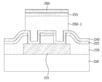
다음으로 도 2h에 도시된 바와 같이, 상기 식각된 폴리이마이드(245-1) 내부의 노출된 시드층(240) 상에 상부 금속 배선을 형성한다. 예컨대, 상기 구리 시드층(240) 상에 구리 전기 도금법을 이용하여 구리층(250)을 형성할 수 있다. 이때 상기 구리층(250)의 두께는 10㎛ 이상이 되도록 두껍게 형성될 수 있다.Next, as shown in FIG. 2H, an upper metal line is formed on the exposed
이어서 상기 식각된 폴리이마이드(245-1) 내부에 형성된 구리층(250) 상에 인터페이스 금속층(interface metal layer)을 형성한다. 상기 인터페이스 금속층은 Ni, Pd, 및 Au 중 적어도 하나가 적층될 수 있다. 여기서 Ni는 니켈이고, Pd는 팔라듐(palladium, Pd)이고, Au는 금이다. 예컨대, 상기 구리층(250) 상에 Ni층(255)이 형성되고, 상기 Ni층(255) 상에 Pd 및 Au 중 어느 하나(260)가 형성될 수 있다.Subsequently, an interface metal layer is formed on the
다음으로 도 2i에 도시된 바와 같이, 300 ~ 400℃의 온도로 N2 가스를 이용하여 신터(sinter) 공정을 수행한다. 폴리이마이드는 포토레지스트(photoresist)보다 열적 특성이 좋기 때문에 300 ~ 400℃의 온도로 수행되는 신터 공정이 용이하게 수행될 수 있다. 상기 폴리이마이드(245-2)는 300 ~ 400℃의 온도의 신터 공정에 의하여 물리적 및 열적 안정성이 향상될 수 있다.Next, as shown in FIG. 2I, a sinter process is performed using N 2 gas at a temperature of 300 ° C. to 400 ° C. FIG. Since polyimide has better thermal properties than photoresist, a sintering process performed at a temperature of 300 to 400 ° C. may be easily performed. The polyimide 245-2 may be improved in physical and thermal stability by a sintering process having a temperature of 300 to 400 ° C.
다음으로 도 2j에 도시된 바와 같이, 신터 공정에 의하여 물리적 및 열적 안정성이 향상된 폴리이마이드(245-2) 상에 백그라인딩(Back Grinding) 공정을 위한 테이핑층(taping layer, 265)를 형성한 후 상기 테이핑층(265)에 고착된 반도체 기판(210))의 후면을 그라인딩하는 백그라인딩 공정을 수행한다. 백그라인딩 공정을 수행한 후 상기 테이핑층(265)을 제거한다.Next, as shown in FIG. 2J, after forming a
상기 신터 공정에 의하여 상기 폴리이마이드(245-2)의 물리적 안정성이 향상되므로 추가적인 포토레지스트를 도포하지 않고, 상기 테이핑층(265)을 상기 폴리이마이드(245-2) 상에 바로 형성할 수 있다. Since the physical stability of the polyimide 245-2 is improved by the sintering process, the
다음으로 도 2k에 도시된 바와 같이, 건식 및 습식 식각을 이용하여 폴리이마이드(245-2) 및 시드층(240)의 일부를 제거한다. 예컨대, O2 플라즈마(Plasma)를 이용하는 건식 식각 공정을 수행하여 상기 폴리이마이드(245-2)를 제거하고, 염산(HCL) 또는 황산을 이용한 습식 식각을 통하여 상기 폴리이마이드(245-2) 제거 후 노출되는 시드층(240)을 제거할 수 있다.Next, as shown in FIG. 2K, the polyimide 245-2 and a part of the
이렇게 습식 식각만을 이용하여 폴리이마이드(245-2) 및 시드층(240)을 제거 하기 보다는 폴리이마이드는 건식 식각으로 제거하고 노출되는 시드층은 습식 식각으로 제거함으로써, 습식 식각에 의한 상부 금속 배선의 측벽의 손실을 감소시킬 수 있다.Rather than removing the polyimide 245-2 and the
다음으로 도 2l에 도시된 바와 같이, 상기 니켈층(255), Pd 및 Au 중 어느 하나(260)가 적층된 구조를 갖는 인터페이스 금속층 상에 액티브 본딩부(270)를 본딩한다. 이때 액티브 본딩부(270) 구현 시의 물리적 충격이 구리층(250) 및 완충 하부 금속 배선(215)에 전달될 수 있다.Next, as shown in FIG. 2L, the
본원 발명의 실시 예에 따른 고전압 반도체 소자의 금속 배선 형성 방법은 도 2a에 도시된 바와 같이 상기 완충 하부 금속 배선(215)의 두께를 1㎛ ~ 2㎛가 되도록 두껍게 형성하여 하부 금속 배선(215)과 상부 금속 배선(250)이 모두 두꺼운 Dual Thick Metal 배선 형성 방법을 사용한다.In the method of forming a metal wiring of a high voltage semiconductor device according to an exemplary embodiment of the present invention, as shown in FIG. 2A, the
따라서 액티브 본딩부(270) 구현시 발생하는 물리적 충격은 상기 완충 하부 금속 배선(215)에 의하여 흡수, 완화되어, 상기 완충 하부 금속 배선(215) 하부의 반도체 기판에 위치하는 회로가 보호될 수 있다. 즉 상기 완충 하부 금속 배선(215) 하부의 반도체 기판(210)에 형성된 회로로 전달되는 액티브 본딩시 발생하는 물리적 스트레스를 감소시킬 수 있다. 또한 상기 완충 하부 금속 배선을 두껍게 형성함으로써 온 저항이 감소될 수 있다.Therefore, the physical shock generated when the
이상에서 설명한 본 발명은 상술한 실시 예 및 첨부된 도면에 한정되는 것이 아니고, 본 발명의 기술적 사상을 벗어나지 않는 범위 내에서 여러 가지 치환, 변형 및 변경이 가능하다는 것이 본 발명이 속하는 기술분야에서 종래의 지식을 가진 자에게 있어 명백할 것이다. 따라서, 본 발명의 기술적 범위는 명세서의 상세한 설명에 기재된 내용으로 한정되는 것이 아니라 특허 청구의 범위에 의해 정하여져야만 할 것이다.The present invention described above is not limited to the above-described embodiments and the accompanying drawings, and various substitutions, modifications, and changes can be made without departing from the technical spirit of the present invention. It will be evident to those who have knowledge of. Therefore, the technical scope of the present invention should not be limited to the contents described in the detailed description of the specification but should be defined by the claims.
도 1은 일반적인 고전압 반도체 소자의 금속 배선층의 단면도를 나타낸다. 1 is a cross-sectional view of a metal wiring layer of a general high voltage semiconductor device.
도 2a 내지 도 2l은 본 발명의 실시 예에 따른 금속 배선 형성 방법을 나타 내는 공정 단면도이다.2A through 2L are cross-sectional views illustrating a method of forming metal wirings according to an exemplary embodiment of the present invention.
Claims (12)
Priority Applications (4)
| Application Number | Priority Date | Filing Date | Title |
|---|---|---|---|
| KR1020080112653A KR101023080B1 (en) | 2008-11-13 | 2008-11-13 | Metal wiring of semiconductor device and method of forming the same |
| US12/582,849 US8278754B2 (en) | 2008-11-13 | 2009-10-21 | Metal line in semiconductor device and method for forming the same |
| TW098136080A TW201019413A (en) | 2008-11-13 | 2009-10-23 | Metal line in semiconductor device and method for forming the same |
| CN200910222014A CN101740489A (en) | 2008-11-13 | 2009-11-13 | A metal line of semiconductor device and method of forming the same |
Applications Claiming Priority (1)
| Application Number | Priority Date | Filing Date | Title |
|---|---|---|---|
| KR1020080112653A KR101023080B1 (en) | 2008-11-13 | 2008-11-13 | Metal wiring of semiconductor device and method of forming the same |
Publications (2)
| Publication Number | Publication Date |
|---|---|
| KR20100053838A KR20100053838A (en) | 2010-05-24 |
| KR101023080B1 true KR101023080B1 (en) | 2011-03-24 |
Family
ID=42164449
Family Applications (1)
| Application Number | Title | Priority Date | Filing Date |
|---|---|---|---|
| KR1020080112653A Expired - Fee Related KR101023080B1 (en) | 2008-11-13 | 2008-11-13 | Metal wiring of semiconductor device and method of forming the same |
Country Status (4)
| Country | Link |
|---|---|
| US (1) | US8278754B2 (en) |
| KR (1) | KR101023080B1 (en) |
| CN (1) | CN101740489A (en) |
| TW (1) | TW201019413A (en) |
Families Citing this family (2)
| Publication number | Priority date | Publication date | Assignee | Title |
|---|---|---|---|---|
| US20150255362A1 (en) * | 2014-03-07 | 2015-09-10 | Infineon Technologies Ag | Semiconductor Device with a Passivation Layer and Method for Producing Thereof |
| KR102666511B1 (en) * | 2023-08-31 | 2024-05-21 | (주)엠케이켐앤텍 | Semiconductor package substrate and semiconductor package including the same |
Citations (4)
| Publication number | Priority date | Publication date | Assignee | Title |
|---|---|---|---|---|
| JPS6294964A (en) * | 1985-10-21 | 1987-05-01 | Nec Corp | Bump construction |
| JP2000294593A (en) * | 1999-04-08 | 2000-10-20 | Nec Corp | Terminal structure of integrated circuit |
| US6144100A (en) * | 1997-06-05 | 2000-11-07 | Texas Instruments Incorporated | Integrated circuit with bonding layer over active circuitry |
| KR20060024928A (en) * | 2004-09-15 | 2006-03-20 | 삼성전자주식회사 | Microelectronic device chip comprising a hybrid bump, a package thereof, a liquid crystal display device comprising the same and a manufacturing method of such a microelectronic device chip |
Family Cites Families (1)
| Publication number | Priority date | Publication date | Assignee | Title |
|---|---|---|---|---|
| US6806578B2 (en) * | 2000-03-16 | 2004-10-19 | International Business Machines Corporation | Copper pad structure |
-
2008
- 2008-11-13 KR KR1020080112653A patent/KR101023080B1/en not_active Expired - Fee Related
-
2009
- 2009-10-21 US US12/582,849 patent/US8278754B2/en active Active
- 2009-10-23 TW TW098136080A patent/TW201019413A/en unknown
- 2009-11-13 CN CN200910222014A patent/CN101740489A/en active Pending
Patent Citations (4)
| Publication number | Priority date | Publication date | Assignee | Title |
|---|---|---|---|---|
| JPS6294964A (en) * | 1985-10-21 | 1987-05-01 | Nec Corp | Bump construction |
| US6144100A (en) * | 1997-06-05 | 2000-11-07 | Texas Instruments Incorporated | Integrated circuit with bonding layer over active circuitry |
| JP2000294593A (en) * | 1999-04-08 | 2000-10-20 | Nec Corp | Terminal structure of integrated circuit |
| KR20060024928A (en) * | 2004-09-15 | 2006-03-20 | 삼성전자주식회사 | Microelectronic device chip comprising a hybrid bump, a package thereof, a liquid crystal display device comprising the same and a manufacturing method of such a microelectronic device chip |
Also Published As
| Publication number | Publication date |
|---|---|
| CN101740489A (en) | 2010-06-16 |
| US20100117233A1 (en) | 2010-05-13 |
| TW201019413A (en) | 2010-05-16 |
| US8278754B2 (en) | 2012-10-02 |
| KR20100053838A (en) | 2010-05-24 |
Similar Documents
| Publication | Publication Date | Title |
|---|---|---|
| JP5605429B2 (en) | Wiring board with built-in semiconductor element | |
| TWI492354B (en) | Semiconductor device and method of manufacturing same | |
| CN102315188B (en) | Method for forming semiconductor die and conductive pillar | |
| US8039385B1 (en) | IC devices having TSVS including protruding tips having IMC blocking tip ends | |
| US10074584B2 (en) | Method of forming a semiconductor component comprising a second passivation layer having a first opening exposing a bond pad and a plurality of second openings exposing a top surface of an underlying first passivation layer | |
| JP5205066B2 (en) | Semiconductor device and manufacturing method thereof | |
| CN102148203B (en) | Semiconductor chip and method of forming conductor pillar | |
| CN104465576B (en) | Semiconductor device and method for manufacturing the same | |
| CN102054790A (en) | Semiconductor device and method for manufacturing the same | |
| JP2009071045A (en) | Semiconductor device and manufacturing method thereof | |
| CN102208409A (en) | Integrated circuit structure | |
| JP5627835B2 (en) | Semiconductor device and manufacturing method of semiconductor device | |
| WO2010047228A1 (en) | Wiring board and method for manufacturing same | |
| KR101023080B1 (en) | Metal wiring of semiconductor device and method of forming the same | |
| JP2012119444A (en) | Semiconductor device | |
| CN118676110A (en) | Substrate wiring structure and preparation method thereof | |
| KR100896841B1 (en) | Bond pad formation method in semiconductor device manufacturing | |
| JP2013065890A (en) | Semiconductor device and manufacturing method of the same | |
| JP2013239756A (en) | Semiconductor device | |
| KR20100079138A (en) | Metal line of power integrated circuit and method for forming the same | |
| JP2014179657A (en) | Semiconductor device |
Legal Events
| Date | Code | Title | Description |
|---|---|---|---|
| A201 | Request for examination | ||
| PA0109 | Patent application |
St.27 status event code: A-0-1-A10-A12-nap-PA0109 |
|
| PA0201 | Request for examination |
St.27 status event code: A-1-2-D10-D11-exm-PA0201 |
|
| D13-X000 | Search requested |
St.27 status event code: A-1-2-D10-D13-srh-X000 |
|
| D14-X000 | Search report completed |
St.27 status event code: A-1-2-D10-D14-srh-X000 |
|
| PG1501 | Laying open of application |
St.27 status event code: A-1-1-Q10-Q12-nap-PG1501 |
|
| E902 | Notification of reason for refusal | ||
| PE0902 | Notice of grounds for rejection |
St.27 status event code: A-1-2-D10-D21-exm-PE0902 |
|
| E13-X000 | Pre-grant limitation requested |
St.27 status event code: A-2-3-E10-E13-lim-X000 |
|
| P11-X000 | Amendment of application requested |
St.27 status event code: A-2-2-P10-P11-nap-X000 |
|
| P13-X000 | Application amended |
St.27 status event code: A-2-2-P10-P13-nap-X000 |
|
| E701 | Decision to grant or registration of patent right | ||
| PE0701 | Decision of registration |
St.27 status event code: A-1-2-D10-D22-exm-PE0701 |
|
| GRNT | Written decision to grant | ||
| PR0701 | Registration of establishment |
St.27 status event code: A-2-4-F10-F11-exm-PR0701 |
|
| PR1002 | Payment of registration fee |
St.27 status event code: A-2-2-U10-U11-oth-PR1002 Fee payment year number: 1 |
|
| PG1601 | Publication of registration |
St.27 status event code: A-4-4-Q10-Q13-nap-PG1601 |
|
| L13-X000 | Limitation or reissue of ip right requested |
St.27 status event code: A-2-3-L10-L13-lim-X000 |
|
| U15-X000 | Partial renewal or maintenance fee paid modifying the ip right scope |
St.27 status event code: A-4-4-U10-U15-oth-X000 |
|
| FPAY | Annual fee payment |
Payment date: 20140217 Year of fee payment: 4 |
|
| PR1001 | Payment of annual fee |
St.27 status event code: A-4-4-U10-U11-oth-PR1001 Fee payment year number: 4 |
|
| FPAY | Annual fee payment |
Payment date: 20150206 Year of fee payment: 5 |
|
| PR1001 | Payment of annual fee |
St.27 status event code: A-4-4-U10-U11-oth-PR1001 Fee payment year number: 5 |
|
| FPAY | Annual fee payment |
Payment date: 20160204 Year of fee payment: 6 |
|
| PR1001 | Payment of annual fee |
St.27 status event code: A-4-4-U10-U11-oth-PR1001 Fee payment year number: 6 |
|
| PR1001 | Payment of annual fee |
St.27 status event code: A-4-4-U10-U11-oth-PR1001 Fee payment year number: 7 |
|
| PN2301 | Change of applicant |
St.27 status event code: A-5-5-R10-R13-asn-PN2301 St.27 status event code: A-5-5-R10-R11-asn-PN2301 |
|
| LAPS | Lapse due to unpaid annual fee | ||
| PC1903 | Unpaid annual fee |
St.27 status event code: A-4-4-U10-U13-oth-PC1903 Not in force date: 20180311 Payment event data comment text: Termination Category : DEFAULT_OF_REGISTRATION_FEE |
|
| PC1903 | Unpaid annual fee |
St.27 status event code: N-4-6-H10-H13-oth-PC1903 Ip right cessation event data comment text: Termination Category : DEFAULT_OF_REGISTRATION_FEE Not in force date: 20180311 |
|
| R18-X000 | Changes to party contact information recorded |
St.27 status event code: A-5-5-R10-R18-oth-X000 |
|
| P22-X000 | Classification modified |
St.27 status event code: A-4-4-P10-P22-nap-X000 |