KR100965254B1 - Flat panel display panel sealing device and method thereof - Google Patents
Flat panel display panel sealing device and method thereof Download PDFInfo
- Publication number
- KR100965254B1 KR100965254B1 KR1020080105860A KR20080105860A KR100965254B1 KR 100965254 B1 KR100965254 B1 KR 100965254B1 KR 1020080105860 A KR1020080105860 A KR 1020080105860A KR 20080105860 A KR20080105860 A KR 20080105860A KR 100965254 B1 KR100965254 B1 KR 100965254B1
- Authority
- KR
- South Korea
- Prior art keywords
- substrate
- stage
- chamber
- display panel
- mask
- Prior art date
- Legal status (The legal status is an assumption and is not a legal conclusion. Google has not performed a legal analysis and makes no representation as to the accuracy of the status listed.)
- Active
Links
- 238000007789 sealing Methods 0.000 title claims abstract description 51
- 238000000034 method Methods 0.000 title claims description 31
- 239000000758 substrate Substances 0.000 claims abstract description 209
- 239000000565 sealant Substances 0.000 claims abstract description 75
- 238000003825 pressing Methods 0.000 claims description 26
- 239000012530 fluid Substances 0.000 claims description 16
- 239000011521 glass Substances 0.000 claims description 10
- IJGRMHOSHXDMSA-UHFFFAOYSA-N Atomic nitrogen Chemical compound N#N IJGRMHOSHXDMSA-UHFFFAOYSA-N 0.000 claims description 8
- 229910052757 nitrogen Inorganic materials 0.000 claims description 4
- 230000001678 irradiating effect Effects 0.000 claims description 3
- 238000010586 diagram Methods 0.000 description 6
- 239000003990 capacitor Substances 0.000 description 5
- 239000010408 film Substances 0.000 description 5
- 238000010438 heat treatment Methods 0.000 description 5
- 238000003860 storage Methods 0.000 description 5
- 230000000694 effects Effects 0.000 description 3
- 239000004973 liquid crystal related substance Substances 0.000 description 3
- 238000001179 sorption measurement Methods 0.000 description 3
- 238000002347 injection Methods 0.000 description 2
- 239000007924 injection Substances 0.000 description 2
- 238000004519 manufacturing process Methods 0.000 description 2
- 239000000463 material Substances 0.000 description 2
- 239000011159 matrix material Substances 0.000 description 2
- 239000010409 thin film Substances 0.000 description 2
- 239000004593 Epoxy Substances 0.000 description 1
- 238000003848 UV Light-Curing Methods 0.000 description 1
- QVGXLLKOCUKJST-UHFFFAOYSA-N atomic oxygen Chemical compound [O] QVGXLLKOCUKJST-UHFFFAOYSA-N 0.000 description 1
- 230000005281 excited state Effects 0.000 description 1
- 239000000945 filler Substances 0.000 description 1
- 230000005283 ground state Effects 0.000 description 1
- 238000009434 installation Methods 0.000 description 1
- 238000012986 modification Methods 0.000 description 1
- 230000004048 modification Effects 0.000 description 1
- 239000001301 oxygen Substances 0.000 description 1
- 229910052760 oxygen Inorganic materials 0.000 description 1
- 239000007787 solid Substances 0.000 description 1
- 229920001187 thermosetting polymer Polymers 0.000 description 1
Images


Classifications
-
- H—ELECTRICITY
- H05—ELECTRIC TECHNIQUES NOT OTHERWISE PROVIDED FOR
- H05B—ELECTRIC HEATING; ELECTRIC LIGHT SOURCES NOT OTHERWISE PROVIDED FOR; CIRCUIT ARRANGEMENTS FOR ELECTRIC LIGHT SOURCES, IN GENERAL
- H05B33/00—Electroluminescent light sources
- H05B33/02—Details
- H05B33/04—Sealing arrangements, e.g. against humidity
-
- H—ELECTRICITY
- H01—ELECTRIC ELEMENTS
- H01J—ELECTRIC DISCHARGE TUBES OR DISCHARGE LAMPS
- H01J9/00—Apparatus or processes specially adapted for the manufacture, installation, removal, maintenance of electric discharge tubes, discharge lamps, or parts thereof; Recovery of material from discharge tubes or lamps
- H01J9/24—Manufacture or joining of vessels, leading-in conductors or bases
- H01J9/26—Sealing together parts of vessels
- H01J9/261—Sealing together parts of vessels the vessel being for a flat panel display
-
- G—PHYSICS
- G02—OPTICS
- G02F—OPTICAL DEVICES OR ARRANGEMENTS FOR THE CONTROL OF LIGHT BY MODIFICATION OF THE OPTICAL PROPERTIES OF THE MEDIA OF THE ELEMENTS INVOLVED THEREIN; NON-LINEAR OPTICS; FREQUENCY-CHANGING OF LIGHT; OPTICAL LOGIC ELEMENTS; OPTICAL ANALOGUE/DIGITAL CONVERTERS
- G02F1/00—Devices or arrangements for the control of the intensity, colour, phase, polarisation or direction of light arriving from an independent light source, e.g. switching, gating or modulating; Non-linear optics
- G02F1/01—Devices or arrangements for the control of the intensity, colour, phase, polarisation or direction of light arriving from an independent light source, e.g. switching, gating or modulating; Non-linear optics for the control of the intensity, phase, polarisation or colour
- G02F1/13—Devices or arrangements for the control of the intensity, colour, phase, polarisation or direction of light arriving from an independent light source, e.g. switching, gating or modulating; Non-linear optics for the control of the intensity, phase, polarisation or colour based on liquid crystals, e.g. single liquid crystal display cells
- G02F1/133—Constructional arrangements; Operation of liquid crystal cells; Circuit arrangements
- G02F1/1333—Constructional arrangements; Manufacturing methods
- G02F1/1339—Gaskets; Spacers; Sealing of cells
-
- H—ELECTRICITY
- H01—ELECTRIC ELEMENTS
- H01J—ELECTRIC DISCHARGE TUBES OR DISCHARGE LAMPS
- H01J9/00—Apparatus or processes specially adapted for the manufacture, installation, removal, maintenance of electric discharge tubes, discharge lamps, or parts thereof; Recovery of material from discharge tubes or lamps
- H01J9/46—Machines having sequentially arranged operating stations
-
- H—ELECTRICITY
- H05—ELECTRIC TECHNIQUES NOT OTHERWISE PROVIDED FOR
- H05B—ELECTRIC HEATING; ELECTRIC LIGHT SOURCES NOT OTHERWISE PROVIDED FOR; CIRCUIT ARRANGEMENTS FOR ELECTRIC LIGHT SOURCES, IN GENERAL
- H05B33/00—Electroluminescent light sources
- H05B33/10—Apparatus or processes specially adapted to the manufacture of electroluminescent light sources
-
- H—ELECTRICITY
- H10—SEMICONDUCTOR DEVICES; ELECTRIC SOLID-STATE DEVICES NOT OTHERWISE PROVIDED FOR
- H10K—ORGANIC ELECTRIC SOLID-STATE DEVICES
- H10K50/00—Organic light-emitting devices
- H10K50/80—Constructional details
- H10K50/84—Passivation; Containers; Encapsulations
- H10K50/842—Containers
- H10K50/8426—Peripheral sealing arrangements, e.g. adhesives, sealants
-
- H—ELECTRICITY
- H10—SEMICONDUCTOR DEVICES; ELECTRIC SOLID-STATE DEVICES NOT OTHERWISE PROVIDED FOR
- H10K—ORGANIC ELECTRIC SOLID-STATE DEVICES
- H10K59/00—Integrated devices, or assemblies of multiple devices, comprising at least one organic light-emitting element covered by group H10K50/00
- H10K59/80—Constructional details
- H10K59/87—Passivation; Containers; Encapsulations
- H10K59/871—Self-supporting sealing arrangements
- H10K59/8722—Peripheral sealing arrangements, e.g. adhesives, sealants
-
- H—ELECTRICITY
- H10—SEMICONDUCTOR DEVICES; ELECTRIC SOLID-STATE DEVICES NOT OTHERWISE PROVIDED FOR
- H10K—ORGANIC ELECTRIC SOLID-STATE DEVICES
- H10K71/00—Manufacture or treatment specially adapted for the organic devices covered by this subclass
- H10K71/40—Thermal treatment, e.g. annealing in the presence of a solvent vapour
- H10K71/421—Thermal treatment, e.g. annealing in the presence of a solvent vapour using coherent electromagnetic radiation, e.g. laser annealing
-
- H—ELECTRICITY
- H10—SEMICONDUCTOR DEVICES; ELECTRIC SOLID-STATE DEVICES NOT OTHERWISE PROVIDED FOR
- H10K—ORGANIC ELECTRIC SOLID-STATE DEVICES
- H10K71/00—Manufacture or treatment specially adapted for the organic devices covered by this subclass
Landscapes
- Physics & Mathematics (AREA)
- Engineering & Computer Science (AREA)
- Manufacturing & Machinery (AREA)
- Optics & Photonics (AREA)
- Nonlinear Science (AREA)
- Electromagnetism (AREA)
- Chemical & Material Sciences (AREA)
- Crystallography & Structural Chemistry (AREA)
- Mathematical Physics (AREA)
- General Physics & Mathematics (AREA)
- Electroluminescent Light Sources (AREA)
- Liquid Crystal (AREA)
- Devices For Indicating Variable Information By Combining Individual Elements (AREA)
Abstract
본 발명은 제1 기판 및 제2 기판을 셀 실런트에 긴밀하게 밀착시켜, 제1 기판과 제2 기판의 견고한 실링을 형성하여, 셀 실런트의 박리 현상을 방지하는 평판 디스플레이 패널 실링 장치에 관한 것이다.BACKGROUND OF THE INVENTION 1. Field of the Invention The present invention relates to a flat panel display panel sealing apparatus in which a first substrate and a second substrate are brought into close contact with a cell sealant to form a rigid seal between the first substrate and the second substrate, thereby preventing peeling of the cell sealant.
본 발명의 일 실시예에 따른 평판 디스플레이 패널 실링 장치는, 단위 셀의 평판 디스플레이 패널을 설정하는 셀 실런트를 개재하고, 상기 단위 셀들의 외곽에 개재되는 외곽 실런트에 의하여 서로 마주하여 접합되는 제1 기판과 제2 기판을 지지하는 스테이지, 상기 스테이지에 마주 배치되어, 조사되는 광을 상기 셀 실런트에 투과시키는 마스크, 및 상기 마스크와 상기 스테이지 사이에 제공되어 상기 제1 기판 및 상기 제2 기판을 수용하여 가압하는 챔버를 포함한다.A flat panel display panel sealing apparatus according to an embodiment of the present invention includes a first substrate that is bonded to each other by a cell sealant that sets a flat panel display panel of a unit cell and is bonded to each other by an outer sealant interposed between the unit cells. And a stage for supporting the second substrate, a mask disposed opposite to the stage to transmit the irradiated light to the cell sealant, and provided between the mask and the stage to receive the first substrate and the second substrate. And a chamber to pressurize.
Description
본 발명은 평판 디스플레이 패널 실링 장치 및 그 방법에 관한 것으로서, 보다 상세하게는 배면기판과 전면기판을 가압하면서 양 기판 사이의 셀 실런트에 광을 조사하여 양 기판을 실링하는 평판 디스플레이 패널 실링 장치 및 그 방법에 관한 것이다.BACKGROUND OF THE
평판 디스플레이 패널은 액정표시장치, 플라즈마 디스플레이 패널 및 유기발광 표시장치를 포함한다. 편의상, 유기발광 표시장치를 예로 들어 설명한다.The flat panel display panel includes a liquid crystal display, a plasma display panel, and an organic light emitting display. For convenience, the organic light emitting display value will be described as an example.
유기발광 표시장치(organic light emitting diode display)는 정공 주입전극과 유기 발광층 및 전자 주입전극으로 구성되는 유기발광 소자들(organic light emitting diode)을 포함하며, 유기 발광층 내부에서 전자와 정공이 결합하여 생성된 여기자(exciton)가 여기 상태로부터 기저 상태로 떨어질 때 발생하는 에너지에 의하여 발광한다.The organic light emitting diode display includes organic light emitting diodes including a hole injection electrode, an organic light emitting layer, and an electron injection electrode, and is formed by combining electrons and holes in the organic light emitting layer. The excited excitons emit light by the energy generated when they fall from the excited state to the ground state.
유기발광 표시장치는 표시영역에 부화소들을 매트릭스 형상으로 배치하며, 부화소는 유기발광 소자와 구동 회로부를 포함한다. 구동 회로부는 스위칭 트랜지 스터, 구동 트랜지스터 및 저장 캐패시터를 포함한다.The organic light emitting display device arranges subpixels in a matrix form in a display area, and the subpixel includes an organic light emitting element and a driving circuit unit. The drive circuitry includes a switching transistor, a drive transistor and a storage capacitor.
유기발광 표시장치는 배면기판에 부화소들을 형성하고, 배면기판과 전면기판을 실링하여 형성된다. 유기 발광 표시장치의 실링 방법에 레이저를 이용하는 방법이 있다.The organic light emitting display device is formed by forming subpixels on a rear substrate and sealing the rear substrate and the front substrate. There is a method of using a laser in the sealing method of the organic light emitting display.
일례로서, 레이저 실링 방법은 표시영역의 외곽에서 배면기판과 전면기판 사이에 글라스 프리트를 배치하고, 글라스 프리트를 레이저로 가열하여 배면기판과 전면기판을 실링한다.As an example, the laser sealing method arranges a glass frit between the rear substrate and the front substrate outside the display area, and heats the glass frit with a laser to seal the back substrate and the front substrate.
글라스 프리트를 사용하는 레이저 실링 방법은 배면기판 및 전면기판을 글라스 프리트에 긴밀하게 밀착시키지 않으면 글라스 프리트의 박리 문제로 인하여 실링 불량을 발생시킨다.The laser sealing method using glass frit causes a sealing failure due to peeling problem of the glass frit unless the back substrate and the front substrate are closely adhered to the glass frit.
보다 구체적으로 설명하면, 유기발광 표시장치는 낱개로 제조될 수 있으나, 생산성 향상을 위하여 복수 개로 제조될 수 있다. 즉 유기발광 표시장치는, 유기발광 표시장치 1개를 단위 셀로 하고(이하 단위 셀), 단위 셀을 복수로 구비하는 원장기판(原張基板 또는 어레이 기판, 이하 원장기판이라 칭한다) 상태를 경유하여 제조될 수 있다.In more detail, the organic light emitting display devices may be manufactured individually, but a plurality of organic light emitting display devices may be manufactured to improve productivity. That is, the organic light emitting display device uses one organic light emitting display device as a unit cell (hereinafter, referred to as a unit cell) and a state of a mother substrate (hereinafter referred to as a mother substrate) having a plurality of unit cells. Can be prepared.
원장기판에서, 단위 셀은 배면기판과 전면기판 사이의 셀 실런트에 의하여 설정되고, 배면기판과 전면기판은 서로의 사이 외곽에 구비되는 외곽 실런트에 의하여 서로 접합된다. 복수의 단위 셀들은 외곽 실런트에 의하여 외부와 차단된다.In the mother substrate, the unit cells are set by a cell sealant between the rear substrate and the front substrate, and the rear substrate and the front substrate are joined to each other by an outer sealant provided on the outer side of each other. The plurality of unit cells are isolated from the outside by the outer sealant.
레이저 실링 방법은 외곽 실런트로 접합된 원장기판의 셀 실런트를 가열하여 배면기판과 전면기판을 실링하는 데 적용될 수 있다.The laser sealing method can be applied to seal the back substrate and the front substrate by heating the cell sealant of the mother substrate bonded by the outer sealant.
예를 들면, 진공 방식은 배면기판과 전면기판을 진공에서 접합하고, 진공을 대기 상태로 전환하여 배면기판과 전면기판의 내외 압력 차이를 이용하여 셀 실런트를 전면기판에 밀착시키고, 레이저로 셀 실런트를 가열하여 양 기판을 실링한다.For example, in the vacuum method, the rear substrate and the front substrate are bonded in a vacuum, the vacuum is switched to the standby state, and the cell sealant is brought into close contact with the front substrate by using the pressure difference between the back and front substrates, and the cell sealant with a laser. Is heated to seal both substrates.
진공이 불충분한 경우, 즉 내부 압력이 외부 압력에 비하여 충분히 낮지 않은 경우, 배면기판과 전면기판이 충분히 밀착되지 못하여 셀 실런트에서 박리가 일어날 수 있다.If the vacuum is insufficient, that is, the internal pressure is not sufficiently low compared to the external pressure, the back substrate and the front substrate may not be sufficiently in contact with each other and peeling may occur in the cell sealant.
배면기판과 전면기판의 접합시, 내부 압력이 상승하는 것을 내부 볼륨의 증가로 완화하기 위하여, 일측 기판에 캐비티(cavity)를 형성하는 경우, 기판들의 내부 볼륨, 셀 실런트의 배치 및 외곽 실런트의 위치 등에 의해 셀 실런트가 박리될 수 있다.In the case of forming a cavity in one substrate, in order to alleviate the increase in the internal pressure due to the increase of the internal volume when the back substrate and the front substrate are bonded, the internal volume of the substrates, the arrangement of the cell sealant, and the position of the outer sealant The cell sealant may be peeled off by, for example.
본 발명의 일 실시예는 제1 기판 및 제2 기판을 셀 실런트로 긴밀하게 밀착시켜, 제1 기판과 제2 기판의 견고한 실링을 형성하므로 셀 실런트의 박리 현상을 방지하는 평판 디스플레이 패널 실링 장치 및 그 방법에 관한 것이다.According to an embodiment of the present invention, the first and second substrates are in close contact with the cell sealant to form a solid sealing of the first substrate and the second substrate, thereby preventing the peeling phenomenon of the cell sealant; It's about how.
본 발명의 일 실시예는 제1 기판과 제2 기판의 내부 압력이 외부 압력과 같거나 외부 압력보다 높은 경우에도 제1 기판과 제2 기판의 실링을 가능하게 하는 평판 디스플레이 패널 실링 장치 및 그 방법에 관한 것이다.One embodiment of the present invention is a flat panel display panel sealing apparatus and method for enabling sealing of a first substrate and a second substrate even when the internal pressure of the first substrate and the second substrate is equal to or higher than the external pressure. It is about.
본 발명의 일 실시예는 차압이 불충분한 경우 강제 가압이 가능하므로 일측 기판에 캐비티(cavity)를 형성하지 않을 수도 있으므로 기판의 제작 비용을 줄이는 평판 디스플레이 패널 실링 장치 및 그 방법에 관한 것이다.One embodiment of the present invention relates to a flat panel display panel sealing apparatus and method for reducing the manufacturing cost of the substrate because it may not be formed in the cavity (cavity) on one side of the substrate because the forced pressure is possible when the differential pressure is insufficient.
또한 본 발명의 일 실시예는 강제 가압이 가능하므로 차압을 약하게 할 수 있고, 이로 인하여 차압이 지나칠 경우 차압에 의해 셀의 중앙부가 오목하게 들어가면서 발생하는 간섭 무늬 즉, 뉴톤 링(Newton Ring)의 발생을 방지하는 평판 디스플레이 패널 실링 장치 및 그 방법에 관한 것이다.In addition, one embodiment of the present invention is because the forced pressure is possible to weaken the differential pressure, which causes the interference pattern, that is, the generation of the Newton Ring (Newton Ring) generated when the center portion of the cell concave by the differential pressure when the differential pressure is excessive The present invention relates to a flat panel display sealing device and a method thereof.
본 발명의 일 실시예에 따른 평판 디스플레이 패널 실링 장치는, 단위 셀의 평판 디스플레이 패널을 설정하는 셀 셀 실런트를 개재하고, 상기 단위 셀들의 외곽에 개재되는 외곽 실런트에 의하여 서로 마주하여 접합되는 제1 기판과 제2 기판을 지지하는 스테이지, 상기 스테이지에 마주 배치되어, 조사되는 광을 상기 셀 실런트에 투과시키는 마스크, 및 상기 마스크와 상기 스테이지 사이에 제공되어 상기 제1 기판 및 상기 제2 기판을 수용하여 가압하는 챔버를 포함할 수 있다.A flat panel display panel sealing apparatus according to an embodiment of the present invention includes a first cell cell sealant for setting a flat panel display panel of a unit cell and bonded to each other by an outer sealant interposed between the unit cells. A stage for supporting a substrate and a second substrate, a mask disposed opposite to the stage to transmit irradiated light to the cell sealant, and provided between the mask and the stage to receive the first substrate and the second substrate It may include a chamber to pressurize.
본 발명의 일 실시예에 따른 평판 디스플레이 패널 실링 장치는, 상기 챔버 내부로 가압 유체를 공급하는 가압 홀을 포함할 수 있다.The flat panel display panel sealing apparatus according to the exemplary embodiment of the present invention may include a pressing hole for supplying a pressurized fluid into the chamber.
상기 가압 홀은, 상기 제1 기판 및 상기 제2 기판과 마주하는 부분 밖의 상기 스테이지 및 상기 챔버 중 적어도 일측에 형성될 수 있다.The pressing hole may be formed on at least one side of the stage and the chamber outside a portion facing the first substrate and the second substrate.
상기 스테이지는, 상기 제1 기판 및 상기 제2 기판과 마주하는 부분의 밖에서 상기 가압 홀의 외곽을 상기 챔버에 탄성적으로 밀착하여, 상기 챔버와 상기 스테이지 사이에서 기밀 작용하는 제1 오링이 배치되는 제1 오링 홈을 형성할 수 있다.The stage may include a first O-ring having an airtight action between the chamber and the stage by elastically closely contacting an outer portion of the pressing hole to the chamber outside a portion facing the first substrate and the second substrate. 1 O-ring groove can be formed.
본 발명의 일 실시예에 따른 평판 디스플레이 패널 실링 장치는, 상기 가압 홀에 연결되어 상기 가압 유체의 공급을 제어하는 제1 제어 밸브를 포함할 수 있다.The flat panel display panel sealing apparatus according to the exemplary embodiment of the present invention may include a first control valve connected to the pressure hole to control the supply of the pressurized fluid.
상기 스테이지는, 상기 제1 기판 및 상기 제2 기판과 마주하는 부분 내에서 상기 제1 기판에 부압을 작용시키는 부압 홀을 형성할 수 있다. 상기 부압 홀은, 상기 마주하는 부분 내에서 하나 이상으로 형성될 수 있다. 복수로 형성되는 상기 부압 홀들은 상기 마주하는 부분 내에서 격자 형태로 배치될 수 있다.The stage may form a negative pressure hole for applying negative pressure to the first substrate in a portion facing the first substrate and the second substrate. The negative pressure hole may be formed in one or more in the facing portion. The negative pressure holes formed in plural may be arranged in a lattice form within the opposing portions.
상기 스테이지는, 상기 마주하는 부분에서 상기 부압 홀의 외곽을 탄성적으로 밀착하여, 상기 제1 기판과 상기 스테이지 사이에서 기밀 작용하는 제2 오링이 배치되는 제2 오링 홈을 형성할 수 있다.The stage may elastically closely contact an outer portion of the negative pressure hole at the facing portion to form a second O-ring groove in which a second O-ring which is airtightly disposed between the first substrate and the stage is disposed.
본 발명의 일 실시예에 따른 평판 디스플레이 패널 실링 장치는, 상기 부압 홀에 연결되어 상기 부압의 작용을 제어하는 제2 제어 밸브를 포함할 수 있다.The flat panel display panel sealing apparatus according to the exemplary embodiment of the present invention may include a second control valve connected to the negative pressure hole to control the action of the negative pressure.
상기 마스크는, 상기 제1 기판 및 상기 제2 기판과 마주하는 부분 밖에서 상기 챔버에 홀더로 고정되고, 상기 챔버와 마주하는 부분에서 상기 챔버와 상기 마스크 사이에서 기밀 작용하는 제3 오링이 배치되는 제3 오링 홈을 형성할 수 있다.The mask is fixed to the chamber outside the portion facing the first substrate and the second substrate, and the third O-ring is disposed between the chamber and the mask in a portion facing the chamber is disposed; 3 O-ring grooves can be formed.
상기 마스크는, 상기 셀 실런트를 상기 광에 노출시키고, 상기 셀 실런트 이외 부분에 대응하여 형성되는 반사막을 더 포함할 수 있다.The mask may further include a reflective film that exposes the cell sealant to the light and is formed to correspond to a portion other than the cell sealant.
상기 평판 디스플레이 패널은 유기발광 표시장치를 포함할 수 있다. 상기 셀 실런트는 글라스 프리트로 형성될 수 있다. 상기 광은 레이저로 형성될 수 있다.The flat panel display panel may include an organic light emitting display device. The cell sealant may be formed of glass frit. The light may be formed by a laser.
본 발명의 일 실시예에 따른 평판 디스플레이 패널 실링 방법은, 스테이지에 마주하도록 마스크를 챔버에 설치하는 단계, 단위 셀의 평판 디스플레이 패널을 설정하는 셀 실런트를 개재하고, 상기 단위 셀들의 외곽에 개재되는 외곽 실런트에 의하여 서로 마주하여 접합되는 제1 기판과 제2 기판을 상기 스테이지에 로딩하는 단계, 상기 제1 기판 및 상기 제2 기판을 상기 챔버 내에서 가압하는 단계, 및 상기 마스크에 광을 조사하여 상기 마스크를 투과한 상기 광으로 상기 셀 실런트를 가열하여 실링하는 단계를 포함할 수 있다.According to an aspect of the present invention, there is provided a flat panel display panel sealing method including installing a mask in a chamber to face a stage, interposing a cell sealant for setting a flat panel display panel of a unit cell, and interposing an outer portion of the unit cells. Loading the first substrate and the second substrate joined to each other by an outer sealant to the stage, pressing the first substrate and the second substrate in the chamber, and irradiating light to the mask. And heating and sealing the cell sealant with the light transmitted through the mask.
상기 가압하는 단계는, 부압을 작용시켜, 상기 제1 기판을 상기 스테이지에 흡착하는 단계를 더 포함할 수 있다.The pressing may further include applying a negative pressure to adsorb the first substrate to the stage.
상기 가압하는 단계는, 상기 제1 기판 및 상기 제2 기판을 상기 챔버 내로 이동시키는 단계, 이동된 상기 제1 기판 및 상기 제2 기판과 상기 마스크를 얼라인 하는 단계, 및 얼라인 된 상기 제1 기판 및 상기 제2 기판을 가압하는 단계를 포함할 수 있다.The pressing may include moving the first substrate and the second substrate into the chamber, aligning the moved first substrate and the second substrate with the mask, and aligning the first substrate. And pressing the substrate and the second substrate.
상기 가압하는 단계는, 상기 챔버 내에 가압 유체로 압축 공기 또는 질소를 공급할 수 있다.The pressurizing may supply compressed air or nitrogen to the pressurized fluid in the chamber.
본 발명의 일 실시예에 따르면, 제1 기판 및 제2 기판을 챔버에 수용하고 가압하면서 마스크를 투과하는 광으로 양 기판 사이에 제공되는 셀 실런트를 가열하여 양 기판을 실링하므로, 제1 기판 및 제2 기판을 셀 실런트에 긴밀하게 밀착시켜 양 기판의 견고한 실링을 가능하게 하는 효과가 있다. 따라서 셀 실런트의 박리 현상이 방지된다.According to an embodiment of the present invention, since the first substrate and the second substrate is received in the chamber and pressurized by sealing the two substrates by heating the cell sealant provided between the two substrates with light passing through the mask, the first substrate and The second substrate may be closely adhered to the cell sealant to enable a firm sealing of both substrates. Therefore, peeling phenomenon of the cell sealant is prevented.
본 발명의 일 실시예에 따르면, 양 기판의 내부 압력이 외부 압력과 같거나 외부 압력보다 높은 경우에도 양 기판의 실링을 가능하게 하는 효과가 있다.According to one embodiment of the present invention, there is an effect of enabling sealing of both substrates even when the internal pressure of both substrates is equal to or higher than the external pressure.
또한 본 발명의 일 실시예에 따르면, 일측 기판의 캐비티(cavity)를 제거하여 기판의 제작 비용을 줄이는 효과가 있으며, 기판에 간섭 무늬 즉, 뉴톤 링(Newton Ring)이 발생하는 것을 방지하는 효과가 있다.In addition, according to an embodiment of the present invention, by removing the cavity (cavity) of one side of the substrate has the effect of reducing the manufacturing cost, the effect of preventing the occurrence of interference fringes, that is Newton Ring (Newton Ring) on the substrate have.
이하, 첨부한 도면을 참조하여 본 발명의 실시예에 대하여 본 발명이 속하는 기술 분야에서 통상의 지식을 가진 자가 용이하게 실시할 수 있도록 상세히 설명한다. 그러나 본 발명은 여러 가지 상이한 형태로 구현될 수 있으며 여기에서 설명하는 실시예에 한정되지 않는다. 도면에서 본 발명을 명확하게 설명하기 위해서 설명과 관계없는 부분은 생략하였으며, 명세서 전체를 통하여 동일 또는 유사한 구성요소에 대해서는 동일한 참조부호를 붙였다.Hereinafter, exemplary embodiments of the present invention will be described in detail with reference to the accompanying drawings so that those skilled in the art may easily implement the present invention. As those skilled in the art would realize, the described embodiments may be modified in various different ways, all without departing from the spirit or scope of the present invention. In order to clearly illustrate the present invention, parts not related to the description are omitted, and the same or similar components are denoted by the same reference numerals throughout the specification.
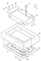
도1은 본 발명의 일 실시예에 따른 평판 디스플레이 패널 실링 장치의 분해 사시도이고, 도2는 도1의 Ⅱ-Ⅱ 선을 따라 자른 단면도이다. 도1 및 도2를 참조하면, 일 실시예에 따른 평판 디스플레이 패널 실링 장치(1)는 스테이지(10)와 마스크(20) 및 챔버(30)를 포함한다.1 is an exploded perspective view of a flat panel display panel sealing apparatus according to an embodiment of the present invention, Figure 2 is a cross-sectional view taken along the line II-II of FIG. 1 and 2, a flat panel display
스테이지(10)는 평판 디스플레이 패널(40)을 형성하는 제1 기판(이하 "배면기판"이라 한다)(41) 및 제2 기판(이하 "전면기판"이라 한다)(42)을 지지하도록 형성된다(도4 참조). 실질적으로, 스테이지(10)는 배면기판(41)과 접촉되어 배면기판(41)을 지지한다. 셀 실런트(43)는 배면기판(41)과 전면기판(42) 사이에 제공된 다(도5 참조).The
본 실시예의 평판 디스플레이 패널 실링 장치(1)에 투입될 때, 배면기판(41)과 전면기판(42)은 단위 셀의 평판 디스플레이 패널(40)을 복수로 구비하는 원장기판 상태이다. 원장기판에서, 셀 실런트(43)는 단위 셀을 설정하고, 외곽 실런트(431)는 단위 셀들의 최외곽에서 배면기판(41)과 전면기판(42)을 서로 접합한다.When inserted into the flat panel display
본 발명의 평판 디스플레이 패널(40)은 액정표시장치, 플라즈마 디스플레이 패널 및 유기발광 표시장치를 포함한다. 편의상, 본 실시예에서는 일례인 유기발광 표시장치에 대하여 주로 설명한다.The flat panel display panel 40 of the present invention includes a liquid crystal display device, a plasma display panel and an organic light emitting display device. For convenience, the organic light emitting display device as an example will mainly be described in this embodiment.
예를 들면, 셀 실런트(43)는 글라스 프리트로 형성될 수 있고, 외곽 실런트(431)는 열경화형 또는 UV경화형 에폭시 실런트로 형성될 수 있다.For example, the
평판 디스플레이 패널(40)이 유기발광 표시장치인 경우, 산소나 수분이 양 기판(41, 42)의 내부로 들어가는 것을 방지할 필요가 있다. 이를 위하여, 외곽 실런트(143)로 양 기판(41, 42)을 먼저 접합하고, 이어서 셀 실런트(43)를 가열하여 양 기판(41, 42)을 실링하는 공정이 진행된다.In the case where the flat panel display panel 40 is an organic light emitting display device, it is necessary to prevent oxygen or moisture from entering the
또한 평판 디스플레이 패널이 액정표시장치 또는 플라즈마 디스플레이 패널인 경우에도 양 기판을 가압하는 경우라면, 양 기판의 외곽부에 외곽 실런트를 도포하여 양 기판을 접합하는 것이 선행될 필요가 있다(미도시).In addition, even when the flat panel display panel is a liquid crystal display device or a plasma display panel, if both substrates are pressurized, it is necessary to apply the outer sealant to the outer portions of both substrates to bond the two substrates (not shown).
본 실시예는 평판 디스플레이 패널(40), 즉 유기발광 표시장치는 서로 마주하는 배면기판(41)과 전면기판(42)을 셀 실런트(43)로 실링하여 형성된다. 서로 마주하는 배면기판(41)과 전면기판(42)의 표시영역에는 부화소들이 매트릭스 형태로 배치된다.In the present exemplary embodiment, the flat panel display panel 40, that is, the organic light emitting display device, is formed by sealing the
도3은 도1에 도시한 평판 디스플레이 패널의 부화소 회로 구조를 나타낸 개략도이고, 도4는 도1에 도시한 평판 디스플레이 패널의 부분 확대 단면도이다.3 is a schematic diagram showing a subpixel circuit structure of the flat panel display panel shown in FIG. 1, and FIG. 4 is a partially enlarged cross-sectional view of the flat panel display panel shown in FIG.
도3 및 도4를 참조하면, 평판 디스플레이 패널(40)에서 부화소는 유기발광 소자(L1)와 구동 회로부로 이루어진다. 유기발광 소자(L1)는 애노드 전극(44)과 유기 발광층(45) 및 캐소드 전극(46)을 포함한다.3 and 4, in the flat panel display panel 40, a subpixel includes an organic light emitting element L1 and a driving circuit unit. The organic light emitting element L1 includes an
구동 회로부는 적어도 2개의 박막 트랜지스터와 적어도 하나의 저장 캐패시터(C1)를 포함한다. 박막 트랜지스터는 기본적으로 스위칭 트랜지스터(T1)와 구동 트랜지스터(T2)를 포함한다.The driving circuit unit includes at least two thin film transistors and at least one storage capacitor C1. The thin film transistor basically includes a switching transistor T1 and a driving transistor T2.
스위칭 트랜지스터(T1)는 스캔 라인(SL1)과 데이터 라인(DL1)에 연결되고, 스캔 라인(SL1)에 입력되는 스위칭 전압에 따라 데이터 라인(DL1)에서 입력되는 데이터 전압을 구동 트랜지스터(T2)로 전송한다.The switching transistor T1 is connected to the scan line SL1 and the data line DL1, and converts the data voltage input from the data line DL1 into the driving transistor T2 according to the switching voltage input to the scan line SL1. send.
저장 캐패시터(C1)는 스위칭 트랜지스터(T1)와 전원 라인(VDD)에 연결되며, 스위칭 트랜지스터(T1)로부터 전송되는 전압과 전원 라인(VDD)에서 공급되는 전압의 차이에 해당하는 전압을 저장한다.The storage capacitor C1 is connected to the switching transistor T1 and the power line VDD and stores a voltage corresponding to a difference between the voltage transmitted from the switching transistor T1 and the voltage supplied from the power line VDD.
구동 트랜지스터(T2)는 전원 라인(VDD)과 저장 캐패시터(C1)에 연결되어 저장 캐패시터(C1)에 저장된 전압과 문턱 전압의 차이의 제곱에 비례하는 출력 전류(IOLED)를 유기발광 소자(L1)로 공급한다. 유기발광 소자(L1)는 출력 전류(IOLED)에 의해 발광한다.The driving transistor T2 is connected to the power supply line VDD and the storage capacitor C1 so that the output current I OLED is proportional to the square of the difference between the voltage stored in the storage capacitor C1 and the threshold voltage. ). The organic light emitting element L1 emits light by the output current I OLED .
구동 트랜지스터(T2)는 소스 전극(47)과 드레인 전극(48) 및 게이트 전극(49)을 포함하며, 유기발광 소자(L1)의 애노드 전극(44)이 구동 트랜지스터(T2)의 드레인 전극(48)에 연결될 수 있다. 부화소의 구성은 전술한 예에 한정되지 않고 다양하게 변형 가능하다.The driving transistor T2 includes a
전면기판(42)은 셀 실런트(43)에 의하여 배면기판(41)에 간격을 두고 실링되어, 배면기판(41)에 형성된 구동 회로부들과 유기발광 소자들을 외부로부터 보호한다.The
한편, 스테이지(10)는 원장기판 상태인 배면기판(41)과 전면기판(42)에서 단위 셀의 실링을 위하여, 외곽 실런트(431)에 의하여 접합된 배면기판(41)과 전면기판(42)을 지지한다.On the other hand, the
다시 도1 및 도2를 참조하면, 스테이지(10)는 셀 실런트(43)를 개재한 배면기판(41) 및 전면기판(42)을 가압할 수 있도록 가압 유체를 공급하기 위한 가압 홀(11)을 형성한다.Referring back to FIGS. 1 and 2, the
예를 들면, 가압 홀(11)은 스테이지(10)에서 배면기판(41) 및 전면기판(42)과 마주하는 부분(FA1) 밖에 형성될 수 있다. 가압 홀(11)은 가압 유체를 챔버(30) 내부에 공급하므로 챔버(30)의 일측에 형성될 수도 있다. 그리고 가압 홀(11)은 하나 또는 복수로 형성될 수 있다.For example, the
도5는 도1에 도시한 평판 디스플레이 패널의 가압 및 레이저 실링 상태도이다. 도5를 참조하면, 가압 홀(11)을 통하여 챔버(30) 내부로 공급되는 가압 유체는 스테이지(10)에 로딩된 배면기판(41) 및 전면기판(42)을 가압(P)하여, 배면기 판(41)과 전면기판(42)을 셀 실런트(43)에 긴밀하게 밀착시킨다.FIG. 5 is a state diagram of pressing and laser sealing of the flat panel display panel shown in FIG. Referring to FIG. 5, the pressurized fluid supplied into the
도2를 참조하면, 가압 홀(11)에 제1 제어 밸브(111)가 연결된다. 제1 제어 밸브(111)는 가압 유체의 공급을 제어하여, 배면기판(41)과 전면기판(42)을 셀 실런트(43)에 밀착되는 정도를 제어한다. 셀 실런트(43)가 배면기판(41)에 도포되는 경우, 가압 유체는 전면기판(42)을 셀 실런트(43)에 밀착시킨다.Referring to FIG. 2, the
효율적인 가압 작용을 위하여, 스테이지(10)와 챔버(30) 사이에 제1 오링(51)이 제공된다. 제1 오링(51)의 위치를 한정하기 위하여, 스테이지(10)는 제1 오링 홈(511)을 형성한다. 제1 오링 홈(511)은 스테이지(10)에서 마주하는 부분(FA1)의 밖이면서 또한 가압 홀(11)의 외곽 위치에 형성된다.For efficient pressing action, a first O-
따라서 제1 오링 홈(511)에 배치되는 제1 오링(51)은 스테이지(10)의 상승시, 챔버(30)에 밀착되어, 스테이지(10)를 챔버(30)에 탄성적으로 밀착하고, 또한 스테이지(10)와 챔버(30) 사이에서 기밀 작용한다.Therefore, the first O-
또한 스테이지(10)는 배면기판(41) 및 전면기판(42)의 가압(P)에 더하여 배면기판(41)을 흡착하도록 부압(V)을 작용하기 위한 부압 홀(12)을 형성한다. 예를 들면, 부압 홀(12)은 스테이지(10)에서 배면기판(41) 및 전면기판(42)과 마주하는 부분(FA1) 내에 형성된다.In addition, the
또한, 부압 홀(12)은 스테이지(10)에서 마주하는 부분(FA1) 내에 하나 이상으로 형성될 수 있다. 부압 홀(12)이 복수로 형성되는 경우, 스테이지(10)에서 마주하는 부분(FA1) 내에 격자 형태로 배치되어, 배면기판(42) 전체 면적에 보다 균일한 부압을 작용시킬 수 있다(도1 및 도2 참조).In addition, the
도2를 참조하면, 부압 홀(12)을 통하여 배면기판(41)에 작용하는 부압(V)은 배면기판(41)을 스테이지(10)에 흡착시킨다. 부압 홀(12)에 제2 제어 밸브(121)가 연결된다. 제2 제어 밸브(121)는 부압(V)의 작용을 제어하여, 배면기판(41)과 전면기판(42)을 스테이지(10)에 흡착되는 정도를 제어한다.Referring to FIG. 2, the negative pressure V acting on the
효율적인 흡착 작용을 위하여, 스테이지(10)와 평판 디스플레이 패널(40)의 배면기판(41) 사이에 제2 오링(52)이 제공된다. 제2 오링(52)의 위치를 한정하기 위하여, 스테이지(10)는 제2 오링 홈(521)을 형성한다. 제2 오링 홈(521)은 스테이지(10)에서 마주하는 부분(FA1)이면서 부압 홀(12)의 외곽 위치에 형성된다.For efficient adsorption, a second O-
따라서 제2 오링 홈(521)에 배치되는 제2 오링(52)은 흡착시, 평판 디스플레이 패널(40)의 배면기판(41)에 밀착되어, 평판 디스플레이 패널(40)을 스테이지(10)에 탄성적으로 밀착하고, 또한 평판 디스플레이 패널(40)과 스테이지(10) 사이에서 기밀 작용한다.Therefore, the second O-
스테이지(10)는 챔버(30)의 하부에 배치되어 챔버(30)를 향하여 승강 작용하고, 마스크(20)는 챔버(30)의 상부에 배치된다.The
마스크(20)는 스테이지(10)에 마주 배치되어, 레이저 건(61)에서 조사되는 레이저(L)를 셀 실런트(43)에 투과시킬 수 있도록 형성된다. 레이저(L)는 셀 실런트(43)를 가열하여 광의 일례이며, 셀 실런트(43)의 재료에 따라 다양한 광이 적용될 수 있다.The
마스크(20)는 평판 디스플레이 패널(40)과 마주하는 부분(FA1) 밖에서 챔버(30)에 홀더(62)로 고정된다. 즉 마스크(20)는 챔버(30)와 마주하는 부분(FA2)에 서 챔버(30)에 장착된다.The
도5를 참조하면, 마스크(20)는 셀 실런트(43)를 레이저에 노출시키고, 셀 실런트(43) 이외 부분에 대응하여 형성되는 반사막(201)을 포함한다. 즉 반사막(201)은 셀 실런트(43) 이외의 부분으로 조사되는 레이저를 반사시켜 셀 실런트(43) 외외 부분이 레이저에 의하여 가열되는 것을 방지하면서, 셀 셀런트(43)만을 레이저로 가열할 수 있게 한다.Referring to FIG. 5, the
본 실시예의 마스크(20)에서, 반사막(201)은 전면기판(42) 측에 형성되어 레이저를 반사하고 있으나, 레이저(L) 및 레이저 건(61) 측에 형성되어 레이저를 더 효과적으로 반사할 수 있다.In the
마스크(20)를 챔버(30)에 설치하고, 마스크(20)의 둘레에 홀더(62)를 배치하며, 홀더(62)를 체결부재(63)로 챔버(30)에 고정시키므로 마스크(20)는 챔버(30)에 고정 설치된다.The
가압 홀(11)로 공급되는 가압 유체의 누출을 방지하기 위하여, 마스크(20)와 챔버(30) 사이에 제3 오링(53)이 제공된다. 제3 오링(53)의 위치를 한정하기 위하여, 마스크(30)는 제3 오링 홈(531)을 형성한다. 제3 오링 홈(531)은 마스크(20)에서 챔버(30)와 마주하는 부분(FA2)에 형성된다.In order to prevent leakage of the pressurized fluid supplied to the
챔버(30)는 서로 마주하는 방향, 즉 상하 방향으로 배치되는 스테이지(10)에서 마스크(20) 쪽으로 개방되는 구조를 형성하며, 스테이지(10)와 마스크(20)의 밀폐 구조에 의하여 가압 공간을 형성한다.The
도6은 본 발명의 일 실시예에 따른 평판 디스플레이 패널 실링 방법의 순서 도이다. 도2 및 도6을 참조하여, 평판 디스플레이 패널 실링 방법에 대하여 설명한다. 평판 디스플레이 패널 실링 방법에 대한 설명은 도1 내지 도5를 참조한 평판 디스플레이 패널 실링 장치(1)의 설명에서 대략적으로 설명되었다.6 is a flowchart of a flat panel display panel sealing method according to an exemplary embodiment of the present invention. 2 and 6, a flat display panel sealing method will be described. Description of the flat panel display panel sealing method has been described in detail in the description of the flat panel display
일 실시예에 따른 평판 디스플레이 패널 실링 방법은, 스테이지(10)에 마주하도록 마스크(20)를 챔버(30)에 설치하는 단계(ST10), 배면기판(41) 및 전면기판(42)을 스테이지(10)에 로딩하는 단계(ST20), 배면기판(41) 및 전면기판(42)을 챔버(30) 내에서 가압하는 단계(ST30), 및 레이저(L)로 셀 실런트(43)를 가열하여 실링하는 단계(ST40)를 포함한다.According to an exemplary embodiment, a flat panel display panel sealing method includes installing a
마스크 설치 단계(ST10)는 마스크(20)를 스테이지(10)에 마주하도록 챔버(30)와 마주하는 부분(FA2)에 배치하고, 체결부재(63)로 홀더(62)를 챔버(30)에 고정시킨다.In the mask installation step ST10, the
로딩 단계(ST20)는 서로 마주하여 접합된 배면기판(41)과 전면기판(42)을 스테이지(10)에 로딩한다. 이때, 배면기판(41)과 전면기판(42)은 단위 셀의 평판 디스플레이 패널(40)을 설정하는 셀 실런트(43)를 개재하고, 단위 셀들의 외곽에 개재되는 외곽 실런트(431)에 의하여 서로 마주하여 접합되는 원장기판 상태이다.The loading step ST20 loads the
가압 단계(ST30)는 스테이지(10)의 가압 홀(11)을 통하여 챔버(30) 내에 가압 유체를 공급하여, 배면기판(41)과 전면기판(42)을 서로 가압한다(P). 따라서 배면기판(41)과 전면기판(42)은 셀 실런트(43)에 밀착된다.In the pressing step ST30, the pressurizing fluid is supplied into the
가압 유체로 압축 공기 또는 질소가 사용될 수 있고, 압축 공기 또는 질소는 배면기판(41) 및 전면기판(42)의 표면에 스크래치를 발생시키지 않는다.Compressed air or nitrogen may be used as the pressurized fluid, and compressed air or nitrogen does not cause scratches on the surfaces of the
가압 단계(ST30)는 흡착 단계(ST31)을 더 포함할 수 있다. 흡착 단계(ST31)는 스테이지(10)의 부압 홀(12)을 통하여 배면기판(41)에 부압(V)을 작용시켜, 배면기판(41)을 스테이지(10)에 흡착하여 더욱 견고하게 고정시킨다.The pressurization step ST30 may further include an adsorption step ST31. In the adsorption step ST31, the negative pressure V is applied to the
가압 단계(ST30)는 이동 단계(ST32), 얼라인 단계(ST33) 및 가압 단계(ST34)를 포함한다. 이동 단계(ST32)는 로딩된 배면기판(41)과 전면기판(42)을 챔버(30) 내부로 이동시킨다.The pressing step ST30 includes a moving step ST32, an alignment step ST33, and a pressing step ST34. The moving step ST32 moves the loaded back
얼라인 단계(ST33)는 이동된 배면기판(41)과 전면기판(42)를 마스크(20)에 얼라인시킨다. 가압 단계(ST34)는 가압 유체를 공급하여 얼라인된 배면기판(41)과 전면기판(42)를 실제로 가압한다.The alignment step ST33 aligns the moved back
실링 단계(ST40)는 레이저 건(61)에서 마스크(20)를 향하여 레이저(L)를 조사하여 셀 실런트(43)를 가열하여 배면기판(41)과 전면기판(42)을 실링한다. 가압 유체는 모든 방향에서, 배면기판(41) 및 전면기판(42)에 균일한 압력을 작용시킨다. 따라서 배면기판(41) 및 전면기판(42)은 균일한 압력을 받게 되고, 이로 인하여 균일하게 셀 실런트(43)에 밀착된다.In the sealing step ST40, the
도7은 도1에 도시한 평판 디스플레이 패널의 내부 충전(充塡)시, 글라스 프리트의 박리 불량에 대응하는 실링 상태도이다.FIG. 7 is a sealing state diagram corresponding to poor peeling of the glass frit during internal charging of the flat panel display panel shown in FIG.
도7을 참조하면, 배면기판(41)과 전면기판(42)의 내부가 충전되어, 예를 들면, 충전재(71) 및 댐(72)이 형성되어 일측 기판(예를 들면, 배면기판)과 셀 실런트(43)가 이격되어 있는 경우에도, 일 실시예의 평판 디스플레이 패널 실링 방법은 효과적으로 적용될 수 있다.Referring to FIG. 7, the inside of the
즉 배면기판(41)과 전면기판(42)을 가압하여(P) 셀 실런트(43)에 밀착한 상태에서, 레이저(L)를 조사하여 셀 실런트(43)를 가열하므로 배면기판(41)과 전면기판(42)은 견고히 실링될 수 있다.That is, the
이상을 통해 본 발명의 바람직한 실시예에 대하여 설명하였지만, 본 발명은 이에 한정되는 것이 아니고 특허청구범위와 발명의 상세한 설명 및 첨부한 도면의 범위 안에서 여러 가지로 변형하여 실시하는 것이 가능하고 이 또한 본 발명의 범위에 속하는 것은 당연하다.Although the preferred embodiments of the present invention have been described above, the present invention is not limited thereto, and various modifications and changes can be made within the scope of the claims and the detailed description of the invention and the accompanying drawings. Naturally, it belongs to the scope of the invention.
도1은 본 발명의 일 실시예에 따른 평판 디스플레이 패널 실링 장치의 분해 사시도이다.1 is an exploded perspective view of a flat panel display panel sealing apparatus according to an embodiment of the present invention.
도2는 도1의 Ⅱ-Ⅱ 선을 따라 자른 단면도이다.FIG. 2 is a cross-sectional view taken along the line II-II of FIG. 1.
도3은 도1에 도시한 평판 디스플레이 패널의 부화소 회로 구조를 나타낸 개략도이다.FIG. 3 is a schematic diagram showing a subpixel circuit structure of the flat panel display panel shown in FIG.
도4는 도1에 도시한 평판 디스플레이 패널의 부분 확대 단면도이다.4 is a partially enlarged cross-sectional view of the flat panel display panel shown in FIG.
도5는 도1에 도시한 평판 디스플레이 패널의 가압 및 레이저 실링 상태도이다.FIG. 5 is a state diagram of pressing and laser sealing of the flat panel display panel shown in FIG.
도6은 본 발명의 일 실시예에 따른 평판 디스플레이 패널 실링 방법의 순서도이다.6 is a flowchart of a flat panel display panel sealing method according to an exemplary embodiment of the present invention.
도7은 도1에 도시한 평판 디스플레이 패널의 내부 충전(充塡)시, 글라스 프리트의 박리 불량에 대응하는 실링 상태도이다.FIG. 7 is a sealing state diagram corresponding to poor peeling of the glass frit during internal charging of the flat panel display panel shown in FIG.
<도면의 주요 부분에 대한 부호의 설명><Explanation of symbols for the main parts of the drawings>
1 : 평판 디스플레이 패널 실링 장치 10 : 스테이지1: flat panel display panel sealing device 10: stage
11 : 가압 홀 12 : 부압 홀11: pressurization hole 12: negative pressure hole
111, 121 : 제1, 제2 제어 밸브 20 : 마스크111, 121: 1st, 2nd control valve 20: mask
30 : 챔버 40 : 평판 디스플레이 패널30 chamber 40 flat panel display panel
41 : 제1 기판(배면기판) 42 : 제2 기판(전면기판)41: first substrate (back substrate) 42: second substrate (front substrate)
43 : 셀 실런트 51, 52, 53 : 제1, 제2, 제3 오링43:
511, 521, 531 : 제1, 제2, 제3 오링 홈 62 : 홀더511, 521, 531: 1st, 2nd, 3rd O-ring groove 62: Holder
63 : 체결부재 71 : 충전재63
72 : 댐 FA1, FA2 : 마주하는 부분72: dam FA1, FA2: facing part
201 : 반사막 431 : 외곽 실런트201: reflective film 431: outer sealant
Claims (19)
Priority Applications (2)
| Application Number | Priority Date | Filing Date | Title |
|---|---|---|---|
| KR1020080105860A KR100965254B1 (en) | 2008-10-28 | 2008-10-28 | Flat panel display panel sealing device and method thereof |
| US12/607,913 US8113902B2 (en) | 2008-10-28 | 2009-10-28 | Flat display panel sealing apparatus and method of the same |
Applications Claiming Priority (1)
| Application Number | Priority Date | Filing Date | Title |
|---|---|---|---|
| KR1020080105860A KR100965254B1 (en) | 2008-10-28 | 2008-10-28 | Flat panel display panel sealing device and method thereof |
Publications (2)
| Publication Number | Publication Date |
|---|---|
| KR20100046833A KR20100046833A (en) | 2010-05-07 |
| KR100965254B1 true KR100965254B1 (en) | 2010-06-22 |
Family
ID=42117954
Family Applications (1)
| Application Number | Title | Priority Date | Filing Date |
|---|---|---|---|
| KR1020080105860A Active KR100965254B1 (en) | 2008-10-28 | 2008-10-28 | Flat panel display panel sealing device and method thereof |
Country Status (2)
| Country | Link |
|---|---|
| US (1) | US8113902B2 (en) |
| KR (1) | KR100965254B1 (en) |
Families Citing this family (6)
| Publication number | Priority date | Publication date | Assignee | Title |
|---|---|---|---|---|
| JP2012209133A (en) * | 2011-03-30 | 2012-10-25 | Canon Inc | Airtight container, image display device, and manufacturing method thereof |
| US8703365B2 (en) | 2012-03-06 | 2014-04-22 | Apple Inc. | UV mask with anti-reflection coating and UV absorption material |
| US8823003B2 (en) | 2012-08-10 | 2014-09-02 | Apple Inc. | Gate insulator loss free etch-stop oxide thin film transistor |
| US9601557B2 (en) | 2012-11-16 | 2017-03-21 | Apple Inc. | Flexible display |
| US9600112B2 (en) | 2014-10-10 | 2017-03-21 | Apple Inc. | Signal trace patterns for flexible substrates |
| KR102708773B1 (en) | 2016-12-26 | 2024-09-23 | 엘지디스플레이 주식회사 | Flexible display device |
Citations (1)
| Publication number | Priority date | Publication date | Assignee | Title |
|---|---|---|---|---|
| KR100808135B1 (en) | 2007-03-06 | 2008-02-29 | 세종산업(주) | Side sealing device for LCD panel |
Family Cites Families (4)
| Publication number | Priority date | Publication date | Assignee | Title |
|---|---|---|---|---|
| KR20010011121A (en) | 1999-07-26 | 2001-02-15 | 윤종용 | Print circuit board having a vertically mounted 2pin type surface mounting device |
| KR100583316B1 (en) * | 2003-12-11 | 2006-05-25 | 엘지.필립스 엘시디 주식회사 | Apparatus and method for manufacturing flat panel display device |
| KR20090043236A (en) | 2007-10-29 | 2009-05-06 | (주)에스아이티 | Sealing device of display panel and sealing method |
| WO2009139291A1 (en) * | 2008-05-12 | 2009-11-19 | 財団法人山形県産業技術振興機構 | Organic el panel manufacturing method and manufacturing device |
-
2008
- 2008-10-28 KR KR1020080105860A patent/KR100965254B1/en active Active
-
2009
- 2009-10-28 US US12/607,913 patent/US8113902B2/en active Active
Patent Citations (1)
| Publication number | Priority date | Publication date | Assignee | Title |
|---|---|---|---|---|
| KR100808135B1 (en) | 2007-03-06 | 2008-02-29 | 세종산업(주) | Side sealing device for LCD panel |
Also Published As
| Publication number | Publication date |
|---|---|
| US8113902B2 (en) | 2012-02-14 |
| US20100105277A1 (en) | 2010-04-29 |
| KR20100046833A (en) | 2010-05-07 |
Similar Documents
| Publication | Publication Date | Title |
|---|---|---|
| KR100965254B1 (en) | Flat panel display panel sealing device and method thereof | |
| KR100713987B1 (en) | Substrate adhesion device and sealing method of organic light emitting display device using the same | |
| JP5793302B2 (en) | Method and apparatus for sealing glass packages | |
| KR100959104B1 (en) | Flat panel display panel cutting device | |
| CN100481322C (en) | Substrate bonding method and device | |
| CN101352100A (en) | Method and device for encapsulating organic light emitting diodes | |
| KR101089487B1 (en) | Method of manufacturing the self-luminous panel | |
| KR100337494B1 (en) | A Method For Fabricating An Organic Electro-Luminescence Display Panel Using A Glass Paste And An Organic Electro-Luminescence Display Panel Thereof | |
| KR100722969B1 (en) | Organic light emitting device bonding system | |
| JP4736602B2 (en) | Organic EL element sealing method and sealing device | |
| KR101242724B1 (en) | Vacuum lamination apparatus and method for laminating a film utilizing the same | |
| KR20060079615A (en) | Organic light emitting device encapsulation method | |
| US7943000B2 (en) | Attaching device and method of fabricating organic light emmiting device using the same | |
| KR101213103B1 (en) | bonding device and fa brication method of Light emitting device using thereof | |
| KR101429915B1 (en) | Device for manufacturing light emitting display element | |
| KR101432819B1 (en) | Apparatus for manufacturing organic electroluminescence display device and method of manufacturing the same | |
| KR101528142B1 (en) | Manufacturing method of light emitting display panel | |
| KR101658438B1 (en) | Substrate Bonding Apparatus for Organic Electro Luminescent device | |
| KR20080062183A (en) | Manufacturing apparatus and method of manufacturing a light emitting display device | |
| KR20150077141A (en) | Apparatus for being cemented to oled and method for controlling thereof | |
| KR20070038210A (en) | Manufacturing apparatus and manufacturing method of the electroluminescent display | |
| KR200352811Y1 (en) | electroluminescent pannel and encapsulation appratus thereof | |
| JP2004079231A (en) | Organic EL element sealing method and sealing device | |
| KR100741974B1 (en) | Bonding device and encapsulation method using the same | |
| KR100670256B1 (en) | Flat panel display and manufacturing method |
Legal Events
| Date | Code | Title | Description |
|---|---|---|---|
| A201 | Request for examination | ||
| PA0109 | Patent application |
Patent event code: PA01091R01D Comment text: Patent Application Patent event date: 20081028 |
|
| PA0201 | Request for examination | ||
| PG1501 | Laying open of application | ||
| E701 | Decision to grant or registration of patent right | ||
| PE0701 | Decision of registration |
Patent event code: PE07011S01D Comment text: Decision to Grant Registration Patent event date: 20100531 |
|
| GRNT | Written decision to grant | ||
| PR0701 | Registration of establishment |
Comment text: Registration of Establishment Patent event date: 20100614 Patent event code: PR07011E01D |
|
| PR1002 | Payment of registration fee |
Payment date: 20100614 End annual number: 3 Start annual number: 1 |
|
| PG1601 | Publication of registration | ||
| FPAY | Annual fee payment |
Payment date: 20130530 Year of fee payment: 4 |
|
| PR1001 | Payment of annual fee |
Payment date: 20130530 Start annual number: 4 End annual number: 4 |
|
| FPAY | Annual fee payment |
Payment date: 20140530 Year of fee payment: 5 |
|
| PR1001 | Payment of annual fee |
Payment date: 20140530 Start annual number: 5 End annual number: 5 |
|
| FPAY | Annual fee payment |
Payment date: 20150601 Year of fee payment: 6 |
|
| PR1001 | Payment of annual fee |
Payment date: 20150601 Start annual number: 6 End annual number: 6 |
|
| FPAY | Annual fee payment |
Payment date: 20170704 Year of fee payment: 8 |
|
| PR1001 | Payment of annual fee |
Payment date: 20170704 Start annual number: 8 End annual number: 8 |
|
| FPAY | Annual fee payment |
Payment date: 20190529 Year of fee payment: 10 |
|
| PR1001 | Payment of annual fee |
Payment date: 20190529 Start annual number: 10 End annual number: 10 |
|
| PR1001 | Payment of annual fee |
Payment date: 20200527 Start annual number: 11 End annual number: 11 |
|
| PR1001 | Payment of annual fee |
Payment date: 20210601 Start annual number: 12 End annual number: 12 |
|
| PR1001 | Payment of annual fee |
Payment date: 20220523 Start annual number: 13 End annual number: 13 |
|
| PR1001 | Payment of annual fee |
Payment date: 20230601 Start annual number: 14 End annual number: 14 |
|
| PR1001 | Payment of annual fee |
Payment date: 20240523 Start annual number: 15 End annual number: 15 |