KR100922681B1 - Charge pump circuit - Google Patents
Charge pump circuit Download PDFInfo
- Publication number
- KR100922681B1 KR100922681B1 KR1020080017707A KR20080017707A KR100922681B1 KR 100922681 B1 KR100922681 B1 KR 100922681B1 KR 1020080017707 A KR1020080017707 A KR 1020080017707A KR 20080017707 A KR20080017707 A KR 20080017707A KR 100922681 B1 KR100922681 B1 KR 100922681B1
- Authority
- KR
- South Korea
- Prior art keywords
- charge pump
- pump circuit
- potential
- generating charge
- semiconductor substrate
- Prior art date
- Legal status (The legal status is an assumption and is not a legal conclusion. Google has not performed a legal analysis and makes no representation as to the accuracy of the status listed.)
- Expired - Fee Related
Links
Images


Classifications
-
- H—ELECTRICITY
- H02—GENERATION; CONVERSION OR DISTRIBUTION OF ELECTRIC POWER
- H02M—APPARATUS FOR CONVERSION BETWEEN AC AND AC, BETWEEN AC AND DC, OR BETWEEN DC AND DC, AND FOR USE WITH MAINS OR SIMILAR POWER SUPPLY SYSTEMS; CONVERSION OF DC OR AC INPUT POWER INTO SURGE OUTPUT POWER; CONTROL OR REGULATION THEREOF
- H02M3/00—Conversion of DC power input into DC power output
- H02M3/02—Conversion of DC power input into DC power output without intermediate conversion into AC
- H02M3/04—Conversion of DC power input into DC power output without intermediate conversion into AC by static converters
- H02M3/06—Conversion of DC power input into DC power output without intermediate conversion into AC by static converters using resistors or capacitors, e.g. potential divider
- H02M3/07—Conversion of DC power input into DC power output without intermediate conversion into AC by static converters using resistors or capacitors, e.g. potential divider using capacitors charged and discharged alternately by semiconductor devices with control electrode, e.g. charge pumps
-
- G—PHYSICS
- G11—INFORMATION STORAGE
- G11C—STATIC STORES
- G11C5/00—Details of stores covered by group G11C11/00
- G11C5/14—Power supply arrangements, e.g. power down, chip selection or deselection, layout of wirings or power grids, or multiple supply levels
-
- H—ELECTRICITY
- H02—GENERATION; CONVERSION OR DISTRIBUTION OF ELECTRIC POWER
- H02M—APPARATUS FOR CONVERSION BETWEEN AC AND AC, BETWEEN AC AND DC, OR BETWEEN DC AND DC, AND FOR USE WITH MAINS OR SIMILAR POWER SUPPLY SYSTEMS; CONVERSION OF DC OR AC INPUT POWER INTO SURGE OUTPUT POWER; CONTROL OR REGULATION THEREOF
- H02M1/00—Details of apparatus for conversion
- H02M1/0083—Converters characterised by their input or output configuration
- H02M1/009—Converters characterised by their input or output configuration having two or more independently controlled outputs
-
- H—ELECTRICITY
- H02—GENERATION; CONVERSION OR DISTRIBUTION OF ELECTRIC POWER
- H02M—APPARATUS FOR CONVERSION BETWEEN AC AND AC, BETWEEN AC AND DC, OR BETWEEN DC AND DC, AND FOR USE WITH MAINS OR SIMILAR POWER SUPPLY SYSTEMS; CONVERSION OF DC OR AC INPUT POWER INTO SURGE OUTPUT POWER; CONTROL OR REGULATION THEREOF
- H02M3/00—Conversion of DC power input into DC power output
- H02M3/02—Conversion of DC power input into DC power output without intermediate conversion into AC
- H02M3/04—Conversion of DC power input into DC power output without intermediate conversion into AC by static converters
- H02M3/06—Conversion of DC power input into DC power output without intermediate conversion into AC by static converters using resistors or capacitors, e.g. potential divider
- H02M3/07—Conversion of DC power input into DC power output without intermediate conversion into AC by static converters using resistors or capacitors, e.g. potential divider using capacitors charged and discharged alternately by semiconductor devices with control electrode, e.g. charge pumps
- H02M3/071—Conversion of DC power input into DC power output without intermediate conversion into AC by static converters using resistors or capacitors, e.g. potential divider using capacitors charged and discharged alternately by semiconductor devices with control electrode, e.g. charge pumps adapted to generate a negative voltage output from a positive voltage source
Landscapes
- Engineering & Computer Science (AREA)
- Power Engineering (AREA)
- Dc-Dc Converters (AREA)
- Semiconductor Integrated Circuits (AREA)
- Electronic Switches (AREA)
Abstract
본 발명은 전위를 발생하는 부전위 발생 차지 펌프 회로와 정전위를 발생하는 정전위 발생 차지 펌프 회로를 구비한 차지 펌프 회로에 있어서, 기생 바이폴라 트랜지스터가 온하는 것을 방지하여, 차지 펌프 회로의 승압 동작을 정상적으로 행한다. 우선, 부전위 발생 차지 펌프 회로(112)를 동작시켜, 출력 전위 LV로서 -VDD를 발생시킨다. 출력 전위 LV는 P형 반도체 기판(10)에 인가되기 때문에, P형 반도체 기판(10)의 전위는 -VDD로 된다. 그 후, 부전위 발생 차지 펌프 회로(112)의 동작을 계속시키면서, 정전위 발생 차지 펌프 회로(111)의 동작을 개시한다. P형 반도체 기판(10)의 전위는 -VDD로 되어 있기 때문에, 정전위 발생 차지 펌프 회로(111)는 정상적으로 동작한다. 정전위 발생 차지 펌프 회로(111)의 출력 전위 HV가 2VDD로 된 후, 부전위 발생 차지 펌프 회로(112)를 상기 제2 동작 모드(HV의 반전 동작)로 동작시킨다.According to the present invention, in a charge pump circuit having a negative potential generating charge pump circuit for generating a potential and an electrostatic potential generating charge pump circuit for generating a static potential, the parasitic bipolar transistor is prevented from turning on, thereby boosting the charge pump circuit. Normally. First, the negative potential generating charge pump circuit 112 is operated to generate -VDD as the output potential LV. Since the output potential LV is applied to the P-type semiconductor substrate 10, the potential of the P-type semiconductor substrate 10 is -VDD. Thereafter, the operation of the negative potential generating charge pump circuit 111 is started while the operation of the negative potential generating charge pump circuit 112 is continued. Since the potential of the P-type semiconductor substrate 10 is -VDD, the positive potential generating charge pump circuit 111 operates normally. After the output potential HV of the positive potential generating charge pump circuit 111 becomes 2 VDD, the negative potential generating charge pump circuit 112 is operated in the second operation mode (inverting operation of HV).
정전위, 부전위, 웰, 차지 펌프 회로, 다이오드, 클램프, 확산층 Potential, Potential, Well, Charge Pump Circuit, Diode, Clamp, Diffusion Layer
Description
본 발명은, 차지 펌프 회로에 관한 것이며, 특히 부전위를 발생하는 부전위 발생 차지 펌프 회로와 정전위를 발생하는 정전위 발생 차지 펌프 회로를 구비한 차지 펌프 회로에 관한 것이다.BACKGROUND OF THE
일반적으로, 차지 펌프 회로는, 전하 전송 MOS 트랜지스터를 직렬 접속하여 복수단의 펌핑 패킷을 구성하여 입력 전위를 승압하는 회로이며, 예를 들면, 표시 장치의 구동 회로의 전원 회로에 널리 이용되고 있다.In general, the charge pump circuit is a circuit for boosting an input potential by connecting a charge transfer MOS transistor in series to form a plurality of pumping packets, and is widely used in, for example, a power supply circuit of a drive circuit of a display device.
구동 회로 등의 LSI에 있어서는, 접지 전위 VSS를 기준으로서 정전위와 부전위를 필요로 하는 경우가 있다. 그 경우, 부전위를 발생하는 부전위 발생 차지 펌프 회로와 정전위를 발생하는 정전위 발생 차지 펌프 회로가 하나의 P형 반도체 기판 위에 형성된다.In LSIs such as drive circuits, a potential of potential and a potential of negative potential may be required based on ground potential VSS. In that case, a negative potential generating charge pump circuit for generating a negative potential and a positive potential generating charge pump circuit for generating a static potential are formed on one P-type semiconductor substrate.
부전위 발생 차지 펌프 회로에 의해 발생된 부전위가 P형 반도체 기판에 인가된다. 또한,P형 반도체 기판의 표면에 N형 웰이 형성되고, 그 N형 웰에 정전위 발생 차지 펌프 회로가 형성되며, 그 정전위가 N형 웰에 인가된다.The negative potential generated by the negative potential generating charge pump circuit is applied to the P-type semiconductor substrate. Further, an N-type well is formed on the surface of the P-type semiconductor substrate, an electrostatic potential generating charge pump circuit is formed in the N-type well, and the positive potential is applied to the N-type well.
상기 차지 펌프 회로에 있어서, 정전위 발생 차지 펌프 회로와 부전위 발생 차지 펌프 회로를 동시에 동작 개시하거나, 정전위 발생 차지 펌프 회로를 먼저 동작시켜 정전위를 발생시키고, 그 정전위를 이용하여 부전위 발생 차지 펌프 회로를 동작시키고 있었다.In the charge pump circuit, the positive potential generating charge pump circuit and the negative potential generating charge pump circuit are started to operate at the same time, or the positive potential generating charge pump circuit is operated first to generate the static potential, and the negative potential is used by using the static potential. The generation charge pump circuit was operating.
차지 펌프 회로에 대해서는 특허 문헌 1, 2에 기재되어 있다.The charge pump circuit is described in
[특허 문헌 1] 일본 특허 공개 제2001-231249호 공보[Patent Document 1] Japanese Patent Application Laid-Open No. 2001-231249
[특허 문헌 2] 일본 특허 공개 제2001-286125호 공보[Patent Document 2] Japanese Patent Application Laid-Open No. 2001-286125
그러나, 상기 차지 펌프 회로에 있어서는, 승압을 정상으로 행할 수 없다는 문제가 있었다. 그 원인에 대하여 도 14를 이용하여 설명한다. P형 반도체 기판(10)의 표면에 N형 웰(11)이 형성되고, 그 N형 웰(11) 내에 정전위 발생 차지 펌프 회로의 전하 전송 MOS 트랜지스터 MP가 형성된다. 전하 전송 MOS 트랜지스터는 복수인데, 도 14에 있어서는, 정전위 발생 차지 펌프 회로의 출력 전위 HV를 출력하는 최종단의 전하 전송 MOS 트랜지스터 MP를 나타내고 있다. 정전위 발생 차지 펌프 회로의 양의 출력 전위 HV는, N형 웰(11)의 표면에 형성된 N+확산층(12)을 개재하여 N형 웰(11)에 인가된다.However, in the above charge pump circuit, there was a problem in that the boosting could not be performed normally. The cause is demonstrated using FIG. An N-
또한,N형 웰(11)과 인접한 P형 반도체 기판(10)의 표면에는, N채널형 MOS 트랜지스터 MN이 형성되어 있다. 이 N채널형 MOS 트랜지스터 MN은 예를 들면 부전위 발생 차지 펌프 회로에 클럭을 공급하는 클럭 드라이버의 N채널형 MOS 트랜지스터이며, 그 소스인 N+형 확산층(13)에 접지 전위 VSS가 인가되어 있다.In addition, an N-channel MOS transistor MN is formed on the surface of the P-
또한,N채널형 MOS 트랜지스터 MN에 인접하여, P형 반도체 기판(10)의 표면에 P+형 확산층(14)이 형성되고, 이 P+형 확산층(14)에 부전위 발생 차지 펌프 회로의 음의 출력 전위 LV(접지 전위 VSS를 기준으로서 음의 전위)가 인가됨으로써, P형 반도체 기판(10)에 음의 출력 전위 LV가 인가되도록 구성되어 있다. 부전위 발생 차지 펌프 회로가 동작하고 있지 않은 상태에서는,P형 반도체 기판(10)은 N+형 확산층(13)에 의해 접지 전위 VSS의 근방에 바이어스되어 있다.Further, a P +
그러나, 정전위 발생 차지 펌프 회로를 동작시키면, 기생 바이폴라 트랜지스터(15)가 온함으로써, P형 반도체 기판(10)에 기판 전류가 흐르고, P형 반도체 기판(10)의 전위가 접지 전위 VSS로부터 플러스측으로 상승한다. 이에 의해,P형 반도체 기판(10)으로부터 N+형 확산층(13)에서 형성되는 기생 다이오드(PN 접합)의 순방향 전류가 흐른다. 그러면, 이 순방향 전류가 기생 바이폴라 트랜지스터(16)의 베이스 전류 IB로 되어, 기생 바이폴라 트랜지스터(16)가 온한다. 이 상태는, 기생 바이폴라 트랜지스터(15, 16)에 의해 형성된 사이리스터가 온한 상태이다.However, when the electrostatic potential generating charge pump circuit is operated, the parasitic
여기서, 기생 바이폴라 트랜지스터(15)의 에미터는 전하 전송 MOS 트랜지스터 MP의 드레인 확산층, 베이스는 N형 웰(11), 콜렉터는 P형 반도체 기판(10)이다. 기생 바이폴라 트랜지스터(16)의 에미터는 N+형 확산층(13), 베이스는 P형 반도체 기판(10), 콜렉터는 N형 웰(11)이다.Here, the emitter of the parasitic
상기 사이리스터가 온하면, 정전위 발생 차지 펌프 회로의 출력단(출력 전위 HV)으로부터, N형 웰(11), P형 반도체 기판(10)을 통하여 접지 전위 VSS에 정상적으로 전류가 흐르기 때문에, 정전위 발생 차지 펌프 회로가 발생하는 정전위가 저하해 버려, 승압 동작을 정상으로 행할 수 없게 된다. 또 P형 반도체 기판(10)의 전위가 상승해 버리기 때문에, 부전위 발생 차지 펌프 회로의 출력 전위는 접지 전위 VSS보다 낮은 전위로 내려갈 수 없는 상태에서 안정되고, 부전위 발생 차지 펌프 회로에 대해서도 승압 동작을 정상으로 행할 수 없게 된다.When the thyristor is turned on, since a current normally flows from the output terminal (output potential HV) of the potential generating charge pump circuit to the ground potential VSS through the N-
본 발명의 차지 펌프 회로는, 정전위를 발생하는 정전위 발생 차지 펌프 회로와, 부전위를 발생하는 부전위 발생 차지 펌프 회로와, 이 부전위 발생 차지 펌프 회로가 발생하는 부전위가 인가되는 제1 도전형 반도체 기판과, 상기 부전위 발생 차지 펌프 회로 및 상기 정전위 발생 차지 펌프 회로의 동작을 제어하는 제어 회로와, 상기 반도체 기판의 표면에 형성되고, 상기 정전위 발생 차지 펌프 회로가 발생하는 정전위가 인가되는 제2 도전형 웰과, 상기 반도체 기판의 표면에 형성된 제2 도전형 확산층과, 상기 정전위 발생 차지 펌프 회로의 동작시에 상기 반도체 기판으로부터 상기 확산층에 순방향 전류가 흐르지 않도록, 상기 반도체 기판의 전위를 클램프하는 클램프용 다이오드를 구비하는 것을 특징으로 한다.The charge pump circuit of the present invention comprises a first in which a static potential generating charge pump circuit for generating a static potential, a negative potential generating charge pump circuit for generating a negative potential, and a negative potential for generating the negative potential generating charge pump circuit are applied. 1 is a conductive semiconductor substrate, a control circuit for controlling the operation of the negative potential generation charge pump circuit and the electrostatic potential generation charge pump circuit, and formed on the surface of the semiconductor substrate, the generation of the electrostatic potential generation charge pump circuit A second conductive well to which a potential is applied, a second conductivity type diffusion layer formed on a surface of the semiconductor substrate, and a forward current from the semiconductor substrate to the diffusion layer during operation of the potential generation charge pump circuit, A clamp diode is provided for clamping the potential of the semiconductor substrate.
이러한 구성에 의하면, 상기 정전위 발생 차지 펌프 회로의 동작시에 상기 클램프용 다이오드에 의해, 상기 반도체 기판의 전위가 클램프되기 때문에 기생 바이폴라 트랜지스터가 온하는 것을 방지할 수 있다.According to this structure, the parasitic bipolar transistor can be prevented from turning on because the potential of the semiconductor substrate is clamped by the clamp diode during the operation of the electrostatic potential generating charge pump circuit.
또한, 본 발명의 차지 펌프 회로는, 정전위를 발생하는 정전위 발생 차지 펌프 회로와, 부전위를 발생하는 부전위 발생 차지 펌프 회로와, 상기 부전위 발생 차지 펌프 회로가 발생하는 부전위가 인가되는 제1 도전형 반도체 기판과, 상기 부전위 발생 차지 펌프 회로 및 상기 정전위 발생 차지 펌프 회로의 동작을 제어하는 제어 회로와, 상기 반도체 기판의 표면에 형성되고, 상기 정전위 발생 차지 펌프 회로가 발생하는 정전위가 인가되는 제2 도전형 웰과, 상기 반도체 기판의 표면에 형성된 제2 도전형 확산층을 구비하고, 상기 제어 회로는 최초로 상기 부전위 발생 차지 펌프 회로의 동작을 개시하여 부전위를 발생시키고, 다음으로, 상기 정전위 발생 차지 펌프 회로의 동작을 개시하여 정전위를 발생시키는 것을 특징으로 한다.In addition, the charge pump circuit of the present invention is applied to the positive potential generating charge pump circuit for generating the static potential, the negative potential generating charge pump circuit for generating the negative potential, and the negative potential generated for the negative potential generating charge pump circuit. A first conductivity type semiconductor substrate, a control circuit for controlling operations of the negative potential generating charge pump circuit and the electrostatic potential generating charge pump circuit, and a surface of the semiconductor substrate, And a second conductivity type diffusion layer to which a generated electrostatic potential is applied, and a second conductivity type diffusion layer formed on a surface of the semiconductor substrate, wherein the control circuit starts operation of the negative potential generation charge pump circuit for the first time. And then, the operation of the electrostatic potential generating charge pump circuit is started to generate the electrostatic potential.
이러한 구성에 의하면, 최초로 상기 부전위 발생 차지 펌프 회로의 동작을 개시하여 부전위를 발생시키고 있기 때문에, 상기 정전위 발생 회로가 동작을 개시한 때에는 상기 반도체 기판은 부전위로 바이어스되어 있어, 기생 바이폴라 트랜지스터가 온하는 것을 방지할 수 있다.According to this structure, since the operation of the negative potential generating charge pump circuit is first started to generate a negative potential, the semiconductor substrate is biased to the negative potential when the constant potential generating circuit starts operation, thereby causing parasitic bipolar transistors. Can be prevented from warming up.
본 발명에 의하면, 부전위를 발생하는 부전위 발생 차지 펌프 회로와 정전위를 발생하는 정전위 발생 차지 펌프 회로를 구비한 차지 펌프 회로에 있어서, 기생 바이폴라 트랜지스터가 온하는 것을 방지하여, 차지 펌프 회로의 승압 동작을 정상적으로 행하는 것이 가능해진다.According to the present invention, in a charge pump circuit having a negative potential generating charge pump circuit for generating a negative potential and an electrostatic potential generating charge pump circuit for generating a static potential, the parasitic bipolar transistor is prevented from turning on and the charge pump circuit It is possible to normally perform the boost operation.
[제1 실시 형태][First Embodiment]
본 발명의 제1 실시 형태에 따른 차지 펌프 회로에 대하여 설명한다. 도 1은 차지 펌프 회로의 블록도이다. 이 차지 펌프 회로는 양의 출력 전위 HV를 발생하는 정전위 발생 차지 펌프 회로(1)와, 음의 출력 전위 LV를 발생하는 부전위 발생 차지 펌프 회로(2)와, 이들 부전위 발생 차지 펌프 회로(2) 및 정전위 발생 차지 펌프 회로(1)의 동작을 제어하는 제어 회로(3)를 P형 반도체 기판 위에 구비하고 있다. 그리고, 부전위 발생 차지 펌프 회로(2)에 의해 발생된 음의 출력 전위 LV가 P형 반도체 기판에 인가된다.The charge pump circuit according to the first embodiment of the present invention will be described. 1 is a block diagram of a charge pump circuit. The charge pump circuit includes a positive potential generating
도 2는 정전위 발생 차지 펌프 회로(1)의 회로도이다. 전하 전송 P채널형 MOS 트랜지스터 MP1, MP2가 직렬로 접속되고, 전하 전송 P채널형 MOS 트랜지스터 MP1의 소스에 입력 전위로서 양의 전원 전위 VDD가 인가되어 있다. 전하 전송 P채널형 MOS 트랜지스터 MP1, MP2의 접속 노드에는 컨덴서 C1의 제1 단자가 접속되어 있다. 또한, 클럭 드라이버로서, 클럭 CLK1이 입력된 CMOS 인버터 INV1이 설치되고, 이 CMOS 인버터 INV1에 의해 클럭 CLK1을 반전한 클럭 *CLK1이 컨덴서 C1의 제2 단자에 인가된다. 전하 전송 P채널형 MOS 트랜지스터 MP1, MP2는, P형 반도체 기판의 표면에 형성되고, 분리된 N형 웰 내에 각각 형성된다.2 is a circuit diagram of the electrostatic potential generating
클럭 CLK1의 로우 레벨은 VSS, 하이 레벨은 VDD이며, CMOS 인버터 INV1의 전원 전위는 VDD이기 때문에, 클럭 *CLK1의 로우 레벨은 VSS, 하이 레벨은 VDD이다. 제어 회로(3)는 클럭 CLK1의 공급과, 전하 전송 P채널형 MOS 트랜지스터 MP1, MP2의 스위칭을 제어한다. 정전위 발생 차지 펌프 회로(1)의 정상 동작 상태에 있어서, MP2의 드레인으로부터 출력 전위 HV(=2VDD)가 얻어진다.Since the low level of the clock CLK1 is VSS and the high level is VDD, and the power supply potential of the CMOS inverter INV1 is VDD, the low level of the clock * CLK1 is VSS and the high level is VDD. The
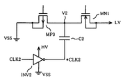
도 3은 부전위 발생 차지 펌프 회로(2)의 회로도이다. 전하 전송 P채널형 MOS 트랜지스터 MP3, 전하 전송 N채널형 MOS 트랜지스터 MN1이 직렬로 접속되고, 전하 전송 P채널형 MOS 트랜지스터 MP3의 소스에 입력 전위로서 접지 전위 VSS가 인가되어 있다.3 is a circuit diagram of the negative potential generating
전하 전송 P채널형 MOS 트랜지스터 MP3은, P형 반도체 기판의 표면에 형성된 N형 웰 내에 형성된다. MP3을 P채널형으로 한 것은, P형 반도체 기판에 부전위 발생 차지 펌프 회로(2)에 의해 발생된 음의 출력 전위 LV가 인가되기 때문이다. 전하 전송 P채널형 MOS 트랜지스터 MP3, 전하 전송 N채널형 MOS 트랜지스터 MN1의 접 속 노드에는 컨덴서 C2의 제1 단자가 접속되어 있다.The charge transfer P-channel MOS transistor MP3 is formed in an N-type well formed on the surface of the P-type semiconductor substrate. MP3 is a P-channel type because a negative output potential LV generated by the negative potential generating
또한, 클럭 드라이버로서, 클럭 CLK2가 입력된 CMOS 인버터 INV2가 형성되고, 이 CMOS 인버터 INV2에 의해 클럭 CLK2를 반전한 클럭 *CLK2가 컨덴서 C2의 제2 단자에 인가된다. 클럭 CLK2는 정전위 발생 차지 펌프 회로(1)가 발생한 출력 전위 HV를 이용하여 작성되고, 그 로우 레벨은 VSS, 하이 레벨은 HV이며, CMOS 인버터 INV2의 전원 전위는 HV이기 때문에, 클럭 *CLK2의 로우 레벨은 VSS, 하이 레벨은 HV이다. 제어 회로(3)는 클럭 CLK2의 공급과, 전하 전송 P채널형 MOS 트랜지스터 MP3, MN1의 스위칭을 제어한다. 부전위 발생 차지 펌프 회로(2)의 정상 동작 상태에 있어서, MN1의 드레인으로부터 출력 전위 LV(=-2VDD)가 얻어진다.As the clock driver, a CMOS inverter INV2 to which the clock CLK2 is input is formed, and a clock * CLK2 inverting the clock CLK2 is applied to the second terminal of the capacitor C2 by the CMOS inverter INV2. The clock CLK2 is created by using the output potential HV generated by the potential generating
도 4는, 차지 펌프 회로를 반도체 기판 위에 형성했을 때의 부분적인 단면도이며, 도 14와 동일한 구성 부분에 대해서는 동일 부호를 붙였다. 정전위 발생 차지 펌프 회로(1), 부전위 발생 차지 펌프 회로(2), 제어 회로(3)는 모두 P형 반도체 기판(10) 위에 형성된다. 도 4의 P채널형 M0S 트랜지스터 MP는, 상기 전하 전송 P채널형 MOS 트랜지스터 MP2에 대응하고, N 채널형 MOS 트랜지스터 MN은, 예를 들면 CMOS 인버터 INV1, INV2의 N채널형 MOS 트랜지스터에 대응하고 있다.4 is a partial cross-sectional view when the charge pump circuit is formed on a semiconductor substrate, and the same components as in FIG. 14 are denoted by the same reference numerals. The positive potential generating
본 실시 형태에 의하면, P형 반도체 기판(10)의 표면에 형성된 P+형 확산층(14)과 접지 전위 VSS 사이에 클램프용 다이오드(20)를 접속하고 있다. 다이오드(20)의 애노드는 P+형 확산층(14)에 접속되고, 캐소드에 접지 전위가 인가된다. 다이오드(20)의 임계치 VF1은 P형 반도체 기판(10)과 N+형 확산층(13)으로 형성되는 다이오드의 임계치 VF2보다 낮은 것이, P형 반도체 기판(10)을 될 수 있는 한 낮은 전위로 클램프하는 점에서 바람직하다. 다이오드(20)의 임계치 VF1이란, 다이오드(20)의 캐소드를 접지하고, 애노드에 정전위를 인가했을 때, 다이오드(20)에 순방향 전류(예를 들면, 1 μA)가 흐를 때의 애노드ㆍ캐소드간 전압이다.According to the present embodiment, the
그러한 다이오드(20)로서는, 쇼트키 배리어 다이오드(VF1=약 0.3 내지 0.4 V)가 적합하다. 이에 대하여, P형 반도체 기판(10)과 N+형 확산층(13)으로 형성되는 다이오드의 순방향의 임계치 VF2는 약 0.7 V이다.As such a
이에 의해, 정전위 발생 차지 펌프 회로(1)가 동작하여, P형 반도체 기판(10)에 기판 전류가 흘러도, P형 반도체 기판(10)의 전위의 상승이 억제된다. 이에 의해,P형 반도체 기판(10)과 N+형 확산층(13)으로 형성되는 기생 다이오드에 순방향 전류가 흐르지 않기 때문에, 기생 바이폴라 트랜지스터(16)가 온하는 것을 방지할 수 있다.Thereby, even if the board | substrate electric current flows in the P-type-semiconductor board |
따라서, 도 5에 도시한 바와 같이, 정전위 발생 차지 펌프 회로(1)를 부전위 발생 차지 펌프 회로(2)보다 먼저 동작을 개시시킨 경우에도, 차지 펌프 회로의 승압 동작을 정상적으로 행할 수 있다.Therefore, as shown in Fig. 5, even when the electrostatic potential generating
다음으로, 정전위 발생 차지 펌프 회로(1), 부전위 발생 차지 펌프 회로(2)의 구체적인 동작에 대하여 설명한다. 우선, 정전위 발생 차지 펌프 회로(1)의 동작에 대하여 도 5, 도 6을 참조하여 설명한다. 도 5에 도시한 바와 같이, 제어 회로(3)에 의해 시각 t1에 있어서 클럭 CLK1의 공급과, MP1, MP2의 스위칭이 개시되면, 정전위 발생 차지 펌프 회로(1)의 동작이 개시된다. 정전위 발생 차지 펌프 회로(1)의 정상 동작 상태에 대하여 도 6을 참조하여 설명한다.Next, specific operations of the electrostatic potential generating
클럭 *CLK1이 로우 레벨일 때, MP1은 온, MP2는 오프이고, MP1과 MP2의 접속 노드의 전위는, 컨덴서 C1이 충전됨으로써 VDD로 된다. 클럭 *CLK1이 하이 레벨일 때, MP1은 오프, MP2는 온이며, MP1과 MP2의 접속 노드의 전위는, 컨덴서 C1의 용량 결합에 의해, VDD로부터 2VDD로 변화한다. 그 2VDD의 전위는 MP2를 통하여 출력된다. 이 동작이 반복됨으로써, 출력 전위 HV로서 2VDD가 얻어진다.When the clock * CLK1 is at the low level, MP1 is on, MP2 is off, and the potential of the connection node of MP1 and MP2 becomes VDD by charging capacitor C1. When the clock * CLK1 is at a high level, MP1 is off and MP2 is on, and the potential of the connection node of MP1 and MP2 changes from VDD to 2VDD by capacitive coupling of capacitor C1. The potential of the 2VDD is output through MP2. By repeating this operation, 2VDD is obtained as the output potential HV.
그 후, 제어 회로(3)에 의해 시각 t2에 있어서 클럭 CLK2의 공급과, MP3, MN1의 스위칭이 개시되면, 부전위 발생 차지 펌프 회로(2)의 동작이 개시된다. 상술한 바와 같이, 클럭 CLK2는 정전위 발생 차지 펌프 회로(1)가 발생한 출력 전위 HV(=2VDD)를 이용하여 작성되고, 그 로우 레벨은 VSS, 하이 레벨은 HV이며, CMOS 인버터 INV2의 전원 전위는 HV이기 때문에, 클럭 *CLK2의 로우 레벨은 VSS, 하이 레벨은 HV이다.Thereafter, when the supply of the clock CLK2 and the switching of the MP3 and the MN1 are started by the
부전위 발생 차지 펌프 회로(2)의 정상 동작 상태에 대하여 도 7을 참조하여 설명한다.The normal operating state of the negative potential generating
클럭 *CLK2이 하이 레벨일 때, MP3은 온, MN1은 오프이며, MP3과 MN1의 접속 노드의 전위는, 컨덴서 C2가 충전됨으로써, VSS로 된다. 클럭 *CLK2가 로우 레벨일 때, MP3은 오프, MN1은 온이며, MP3과 MN1의 접속 노드의 전위는, 컨덴서(2)의 용량 결합에 의해, VSS로부터 -HV(=-2VDD)로 변화한다. 그 -HV의 전위는 MN1을 통하여 출력된다. 이 동작이 반복됨으로써, 출력 전위 LV로서 -HV(=-2VDD)가 얻어진다.When the clock * CLK2 is at the high level, MP3 is on and MN1 is off, and the potential of the connection node of MP3 and MN1 becomes VSS by charging capacitor C2. When the clock * CLK2 is at the low level, MP3 is off and MN1 is on, and the potential of the connection node of MP3 and MN1 changes from VSS to -HV (= -2VDD) by capacitive coupling of the
[제2 실시 형태]Second Embodiment
본 발명의 제2 실시 형태에 따른 차지 펌프 회로에 대하여 설명한다. 제1 실시 형태에 있어서는, 클램프용 다이오드(20)를 형성함으로써, P형 반도체 기판(10)의 전위를 접지 전위 VSS의 근방으로 클램프함으로써, 기생 바이폴라 트랜지스터(16)의 온을 방지했지만, 본 실시 형태에 있어서는, 부전위 발생 차지 펌프 회로(2)를 정전위 발생 차지 펌프 회로(1)보다 먼저 동작시킴으로써, 기생 바이폴라 트랜지스터(16)의 온을 방지한 것이다. 이에 의해, 다이오드(20)를 불필요하게 하여 코스트 다운을 도모할 수 있다.A charge pump circuit according to a second embodiment of the present invention will be described. In the first embodiment, the parasitic
이하, 본 실시 형태의 차지 펌프 회로에 대하여 도면을 참조하여 자세하게 설명한다. 정전위 발생 차지 펌프 회로(1)의 구성에 대해서는 제1 실시 형태의 회로(도 2)와 동일하다. 부전위 발생 차지 펌프 회로(2)는 도 8에 도시한 바와 같이, 클럭 드라이버부의 구성이 제1 실시 형태와 상이하다. 즉, CMOS 인버터 INV2 외에, 클럭 CLK3이 입력된 CMOS 인버터 INV3이 형성되어 있다. CMOS 인버터 INV3에 공급되는 전원 전위는 VDD이다. CMOS 인버터 INV3의 출력은 클럭 CLK3을 반전한 클럭 *CLK3으로 된다.EMBODIMENT OF THE INVENTION Hereinafter, the charge pump circuit of this embodiment is demonstrated in detail with reference to drawings. The configuration of the static potential generating
클럭 CLK2, *CLK2의 로우 레벨은 VSS, 하이 레벨은 HV(정전위 발생 차지 펌프 회로(1)의 출력 전위)이지만, 클럭 CLK3, *CLK3의 로우 레벨은 VSS, 하이 레벨은 VDD이다. 또한,CMOS 인버터 INV2, INV3의 출력을 선택적으로 컨덴서 C2의 제2 단자에 인가하기 위한 스위치 SW1, SW2가, 각각의 출력단에 설치되어 있다. 스위치 SW1, SW2의 온 오프는 도 1의 제어 회로(3)에 의해 제어된다.The low levels of the clocks CLK2 and * CLK2 are VSS, and the high level is HV (the output potential of the potential generating charge pump circuit 1), but the low levels of the clocks CLK3 and * CLK3 are VSS and the high level is VDD. In addition, switches SW1 and SW2 for selectively applying the outputs of the CMOS inverters INV2 and INV3 to the second terminal of the capacitor C2 are provided at the respective output terminals. The on / off of the switches SW1, SW2 is controlled by the
다음으로, 상기 차지 펌프 회로의 동작에 대하여 설명한다. 도 9에 도시한 바와 같이, 제어 회로(3)에 의해 시각 t3에 있어서 클럭 CLK3의 공급과, MP3, MN1의 스위칭이 개시되면, 부전위 발생 차지 펌프 회로(2)의 동작이 개시된다. 이 때, 스위치 SW1은 온, 스위치 SW2는 오프로 설정되고, 클럭 CLK3은 인버터 INV3을 통하여, 컨덴서 C2의 제2 단자에 인가된다. 이 때의 부전위 발생 차지 펌프 회로(2)의 정상 동작 상태에 대하여 도 10을 참조하여 설명한다.Next, the operation of the charge pump circuit will be described. As shown in FIG. 9, when supply of the clock CLK3 and switching of MP3, MN1 are started by the
클럭 *CLK3이 하이 레벨(VDD)일 때, MP3은 온, MN1은 오프이며, MP3과 MN1의 접속 노드의 전위는, 컨덴서 C2가 충전됨으로써, VSS로 된다. 클럭 *CLK3이 로우 레벨(VSS)일 때, MP3은 오프, MN1은 온이며, MP3과 MN1의 접속 노드의 전위는, 컨덴서 C2의 용량 결합에 의해, VSS로부터 -VDD로 변화한다. 그 -VDD의 전위는 MN1을 통하여 출력된다. 이 동작이 반복됨으로써, 출력 전위 LV로서 -VDD가 출력된다. 이에 의해, 출력 전위 LV는 P+형 확산층(14)을 통하여 P형 반도체 기판(10)에 인가되기(도 4 참조) 때문에, P형 반도체 기판(10)은 -VDD로 바이어스된다.When the clock * CLK3 is at the high level (VDD), MP3 is on, MN1 is off, and the potential of the connection node of MP3 and MN1 becomes VSS by charging capacitor C2. When the clock * CLK3 is at the low level (VSS), MP3 is off and MN1 is on, and the potential of the connection node of MP3 and MN1 changes from VSS to -VDD by capacitive coupling of capacitor C2. The potential of the -VDD is output through MN1. By repeating this operation, -VDD is output as the output potential LV. As a result, the output potential LV is applied to the P-
그 후, 제어 회로(3)에 의해 시각 t4에 있어서 클럭 CLK1의 공급과, MP1, MP2의 스위칭이 개시되면, 정전위 발생 차지 펌프 회로(1)의 동작이 개시된다. 정전위 발생 차지 펌프 회로(1)의 동작에 의해 기판 전류가 흐르지만, P형 반도체 기판(10)은 부전위 발생 차지 펌프 회로(2)에 의해 -VDD라는 VSS보다 낮은 전위로 바이어스되어 있기 때문에, 기생 바이폴라 트랜지스터(16)가 온하는 것이 방지된다. 이에 의해, 정전위 발생 차지 펌프 회로(1)는 정상적으로 동작하고, 그 출력 전위 HV로서 2VDD가 출력된다(도 6 참조).Thereafter, when the supply of the clock CLK1 and the switching of the MP1 and the MP2 are started by the
정전위 발생 차지 펌프 회로(1)의 출력 전위 HV가 2VDD에 도달한 후의 시각 t5에 있어서, 스위치 SW1은 오프, 스위치 SW2는 온으로 설정된다. 이에 의해, 클럭 CLK2는 인버터 INV2를 통하여 컨덴서 C2의 제2 단자에 인가된다. 클럭 CLK2는 정전위 발생 차지 펌프 회로(2)가 발생한 출력 전위 HV를 이용하여 작성되고, 그 로우 레벨은 VSS, 하이 레벨은 HV이며, CMOS 인버터 INV2의 전원 전위는 HV이기 때문에, 클럭 *CLK2의 로우 레벨은 VSS, 하이 레벨은 HV이다.At time t5 after the output potential HV of the potential-generated
이에 의해, 부전위 발생 차지 펌프 회로(2)는 진폭이 큰 클럭 CLK2에 기초하여 동작하기 때문에, 그 출력 전위 LV는 더 높은 음의 고전위로 승압되고, -HV(=-2VDD)라는 음의 출력 전위 LV가 얻어진다. 이와 같이 하여, 최종적으로 P형 반도체 기판(10)의 전위는 -HV에 도달한다.Thereby, since the negative potential generation
[제3 실시 형태][Third Embodiment]
본 실시 형태는, 제2 실시 형태와 마찬가지로, 부전위 발생 차지 펌프 회로(2)를 정전위 발생 차지 펌프 회로(1)보다 먼저 동작시킴으로써, 기생 바이폴라 트랜지스터의 온을 방지하는 것이다. 제2 실시 형태와 상이한 것은, 부전위 발생 차지 펌프 회로(2)는, 정전위 발생 차지 펌프 회로(1)에 의해 발생시킨 양의 출력 전위 HV(=2VDD)를 반전하여, -HV(=-2VDD)라는 음의 출력 전위 LV를 발생시키는 점이다.In the present embodiment, similarly to the second embodiment, the negative potential generating
이하, 본 실시 형태의 차지 펌프 회로에 대하여 자세하게 설명한다. 도 11은 이 차지 펌프 회로의 회로도이다. 정전위 발생 차지 펌프 회로(111)는 기본적으로는 제2 실시 형태의 정전위 발생 차지 펌프 회로(1)와 마찬가지이다. 전하 전송 P채널형 M0S 트랜지스터 MP11, MP12가 직렬로 접속되고, MP11의 소스에 입력 전 위로서 양의 전원 전위 VDD가 인가되어 있다. 정상 동작 상태에 있어서, MP12의 드레인으로부터 출력 전위 HV(=2VDD)가 얻어진다.EMBODIMENT OF THE INVENTION Hereinafter, the charge pump circuit of this embodiment is demonstrated in detail. 11 is a circuit diagram of this charge pump circuit. The static potential generating charge pump circuit 111 is basically the same as the static potential generating
MP11, MP12의 접속 노드에는 컨덴서 C11의 제1 단자 C1A가 접속되어 있다. 또한, 클럭 드라이버로서 CMOS 인버터 INV11이 형성되어 있고, 그 출력이 컨덴서 C11의 제2 단자 C1B에 접속되어 있다.The first terminal C1A of the capacitor C11 is connected to the connection node of the MP11 and MP12. In addition, a CMOS inverter INV11 is formed as a clock driver, and its output is connected to the second terminal C1B of the capacitor C11.
CMOS 인버터 INV11은, P채널형 MOS 트랜지스터 MP13과 N채널형 MOS 트랜지스터 MN11을 전원 전위 VDD와 접지 전위 VSS 사이에 직렬로 접속하여 구성되고, MP13의 게이트에 클럭 CLK11이 인가되고, MN11의 게이트에 클럭 CLK12가 인가된다. 클럭 CLK11, 12는 동일한 클럭이며, 그 하이 레벨은 VDD, 로우 레벨은 VSS이다.The CMOS inverter INV11 is configured by connecting a P-channel MOS transistor MP13 and an N-channel MOS transistor MN11 in series between a power supply potential VDD and a ground potential VSS. The clock CLK11 is applied to the gate of the MP13, and the clock is applied to the gate of the MN11. CLK12 is applied. The clocks CLK11 and 12 are the same clock, the high level of which is VDD and the low level of which are VSS.
MP11의 게이트에는 레벨 시프터 LS1로부터의 클럭 CLK13이 인가되고, MP12의 게이트에는 레벨 시프터 LS2로부터의 클럭 CLK14가 인가된다. 클럭 CLK13과 클럭 CLK14는 역상의 클럭이며, MP11과 MP12는 상보적으로 스위칭한다. 클럭 CLK13과 클럭 CLK14의 하이 레벨은 HV(=2VDD), 로우 레벨은 VSS이다.Clock CLK13 from level shifter LS1 is applied to the gate of MP11, and clock CLK14 from level shifter LS2 is applied to the gate of MP12. Clock CLK13 and clock CLK14 are reversed clocks, and MP11 and MP12 switch complementarily. The high level of clock CLK13 and clock CLK14 is HV (= 2VDD), and the low level is VSS.
상기 정전위 발생 차지 펌프 회로(111)의 동작은, 제1 상태(클럭 CLK11, CLK12=하이 레벨)에 있어서,MP13: 오프, MN11: 온, MP11: 온, MP12: 오프이며, 컨덴서 C11의 제2 단자 C1B의 전위는 VSS, 컨덴서 C11의 제1 단자 C1A의 전위는 VDD이다.The operation of the electrostatic potential generating charge pump circuit 111 is MP13: off, MN11: on, MP11: on, MP12: off in the first state (clocks CLK11, CLK12 = high level), and The potential of the two terminals C1B is VSS, and the potential of the first terminal C1A of the capacitor C11 is VDD.
제2 상태(클럭 CLK11, CLK12=로우 레벨)에 있어서, MP13: 온, MN11: 오프, MP11: 오프, MP12: 온이며, 컨덴서 C11의 제2 단자 C1B의 전위는 VDD, 컨덴서 C11의 제1 단자 C1A의 전위는 2VDD이다. 제1 단자 C1A의 전하는 MP12를 통하여, 출력 컨덴서 Cout1에 충전된다. 제1 상태와 제2 상태를 반복함으로써, 출력 전위 HV는 2VDD로 된다.In the second state (clocks CLK11, CLK12 = low level), MP13: on, MN11: off, MP11: off, MP12: on, and the potential of the second terminal C1B of the capacitor C11 is VDD, the first terminal of the capacitor C11. The potential of C1A is 2VDD. Charge of the first terminal C1A is charged to the output capacitor Cout1 via MP12. By repeating the first state and the second state, the output potential HV becomes 2VDD.
다음으로, 부전위 발생 차지 펌프 회로(112)의 구성에 대하여 설명한다. 전하 전송 P채널형 MOS 트랜지스터 MP14, MP15가 직렬로 접속되고, MP14의 소스에 정전위 발생 차지 펌프 회로(111)의 MP12의 드레인이 접속됨으로써, MP14의 소스에, 정전위 발생 차지 펌프 회로(111)의 출력 전위 HV가 인가되도록 되어 있다. MP15의 드레인은 접지되어 있다.Next, the configuration of the negative potential generating charge pump circuit 112 will be described. The charge transfer P-channel MOS transistors MP14 and MP15 are connected in series, and the drain of the MP12 of the electrostatic potential generating charge pump circuit 111 is connected to the source of the MP14, so that the potential of the potential generating charge pump circuit 111 is connected to the source of the MP14. Output potential HV is applied. The drain of the MP15 is grounded.
또한, 접지 전위 VSS와 출력단 사이에, 전하 전송 P채널형 M0S 트랜지스터 MP16, 전하 전송 N채널형 MOS 트랜지스터 MN12가 직렬로 접속되어 있다. MP14와 MP15의 접속점과 MP16과 MN12의 접속점 사이에 컨덴서 C12가 접속되어 있다. 즉, 컨덴서 C12의 제1 단자 C2A는 MP16, MN12의 접속점에 접속되고, 컨덴서 C12의 제2 단자 C2B은 MP14, MN15의 접속점에 접속되어 있다.Further, the charge transfer P-channel MOS transistor MP16 and the charge transfer N-channel MOS transistor MN12 are connected in series between the ground potential VSS and the output terminal. The capacitor C12 is connected between the connection point of MP14 and MP15 and the connection point of MP16 and MN12. That is, the first terminal C2A of the capacitor C12 is connected to the connection points of MP16 and MN12, and the second terminal C2B of the capacitor C12 is connected to the connection points of MP14 and MN15.
MP14의 게이트에는 레벨 시프터 LS3으로부터의 클럭 CLK19가 인가되고, MP15의 게이트에는 레벨 시프터 LS4로부터의 클럭 CLK20이 인가된다. 클럭 CLK19와 클럭 CLK20은 역상의 클럭이며, MP14와 MP15는 상보적으로 스위칭한다. 클럭 CLK19와 클럭 CLK20의 하이 레벨은 HV(=2VDD), 로우 레벨은 VSS이다.The clock CLK19 from the level shifter LS3 is applied to the gate of the MP14, and the clock CLK20 from the level shifter LS4 is applied to the gate of the MP15. Clocks CLK19 and CLK20 are reversed clocks, and MP14 and MP15 switch complementarily. The high level of clock CLK19 and clock CLK20 is HV (= 2VDD), and the low level is VSS.
또한,MP16의 게이트에는 레벨 시프터 LS5로부터의 클럭 CLK17이 인가되고, MN12의 게이트에는 레벨 시프터 LS6으로부터의 클럭 CLK18이 인가된다. 클럭 CLK17, CLK18은 동일한 클럭이며, MP16과 MN12는 상보적으로 스위칭한다.The clock CLK17 from the level shifter LS5 is applied to the gate of the MP16, and the clock CLK18 from the level shifter LS6 is applied to the gate of the MN12. Clocks CLK17 and CLK18 are the same clock, and MP16 and MN12 switch complementarily.
또한,CMOS 인버터 INV12가 형성되고, 그 출력은 제어 신호 ST에 의해 제어 된 트랜스퍼 게이트 TG를 통하여 컨덴서 C12의 제2 단자 C2B에 접속되어 있다. CMOS 인버터 INV12는 P채널형 MOS 트랜지스터 MP17과 N채널형 MOS 트랜지스터 MN13을 VDD와 VSS 사이에 접속하여 구성된다. MP17의 게이트에 클럭 CLK15가 인가되고, MN13의 게이트에 클럭 CLK16이 인가된다. 클럭 CLK15, 16은 동일한 클럭이며, 그 하이 레벨은 VDD, 로우 레벨은 VSS이다.In addition, a CMOS inverter INV12 is formed, and its output is connected to the second terminal C2B of the capacitor C12 via the transfer gate TG controlled by the control signal ST. The CMOS inverter INV12 is configured by connecting a P-channel MOS transistor MP17 and an N-channel MOS transistor MN13 between VDD and VSS. Clock CLK15 is applied to the gate of MP17, and clock CLK16 is applied to the gate of MN13. The clocks CLK15 and 16 are the same clock, and the high level is VDD and the low level is VSS.
상기 부전위 발생 차지 펌프 회로(112)는, 2개의 동작 모드를 갖고 있다. 제1 동작 모드에서는,MP14, MP15는 스위칭 동작을 정지하고 있고, 제어 신호 ST가 하이 레벨로 설정됨으로써 트랜스퍼 게이트 TG는 온하고 있다. 그리고, MP16, MP17, MN12, MN13의 스위칭에 의해, 출력 전위 LV로서 -VDD를 발생한다. 이 동작은, 제1, 제2 실시 형태의 부전위 발생 차지 펌프 회로(2)의 동작과 동일하다.The negative potential generating charge pump circuit 112 has two operating modes. In the first operation mode, the MP14 and MP15 stop the switching operation, and the transfer gate TG is turned on because the control signal ST is set to the high level. Then, by switching the MP16, MP17, MN12, MN13, -VDD is generated as the output potential LV. This operation is the same as that of the negative potential generating
즉, 제1 상태(클럭 CLK15, CLK16=로우 레벨)에 있어서, MP17: 온, MN13: 오프, MP16: 온, MN12: 오프이며, 컨덴서 C12의 제2 단자 C2B의 전위는 VDD, 컨덴서 C12의 제1 단자 C2A의 전위(MP16, MN12의 접속점의 전위)는 VSS이다.That is, in the first state (clocks CLK15, CLK16 = low level), MP17: on, MN13: off, MP16: on, MN12: off, and the potentials of the second terminal C2B of the capacitor C12 are VDD, the first of the capacitor C12. The potential of the one terminal C2A (potential of the connection point of MP16 and MN12) is VSS.
제2 상태(클럭 CLK15, CLK16=하이 레벨)에 있어서, MP17: 오프, MN13: 온, MP16: 오프, MN12: 온이며, 컨덴서 C12의 제2 단자 C2B의 전위는 VSS, 컨덴서 C12의 제1 단자 C2A의 전위는 -VDD이다. 제1 단자 C2A의 전하는 MN12를 통하여, 출력 컨덴서 Cout2에 충전된다. 제1 상태, 제2 상태를 반복함으로써, 출력 전위 LV는 -VDD로 된다.In the second state (clocks CLK15, CLK16 = high level), MP17: off, MN13: on, MP16: off, MN12: on, the potential of the second terminal C2B of the capacitor C12 is VSS, the first terminal of the capacitor C12 The potential of C2A is -VDD. Charge of the first terminal C2A is charged to the output capacitor Cout2 via MN12. By repeating the first state and the second state, the output potential LV becomes -VDD.
한편, 제2 동작 모드에서는, 정전위 발생 차지 펌프 회로(111)가 발생한 양의 출력 전위 HV(=2VDD)를 반전하여, -HV를 발생한다. MP17, MN13은, 스위칭 동작 을 정지하고 있고, 제어 신호 ST가 로우 레벨로 설정됨으로써 트랜스퍼 게이트 TG는 오프되어 있다. 제1 상태에 있어서, MP16: 온, MN12: 오프, MP14: 온, MP15: 오프로 됨으로써, 컨덴서 C12의 제2 단자 C2B의 전위는 HV, 제1 단자 C2A의 전위는 VSS이다. 제2 상태에 있어서, MP16: 오프, MN12: 온, MP14: 오프, MP15: 온으로 됨으로써, 제2 단자 C2B의 전위는 VSS, 제1 단자 C2A의 전위는 -HV로 된다. 제1 상태, 제2 상태를 반복함으로써, 출력 전위 LV는 -HV로 된다.On the other hand, in the second operation mode, the positive potential generating charge pump circuit 111 inverts the positive output potential HV (= 2VDD) to generate -HV. The MP17 and MN13 stop the switching operation, and the transfer gate TG is turned off because the control signal ST is set at the low level. In the first state, MP16: on, MN12: off, MP14: on, MP15: off, the potential of the second terminal C2B of the capacitor C12 is HV, and the potential of the first terminal C2A is VSS. In the second state, MP16: off, MN12: on, MP14: off, MP15: on, the potential of the second terminal C2B is VSS, and the potential of the first terminal C2A is -HV. By repeating the first state and the second state, the output potential LV becomes -HV.
정전위 발생 차지 펌프 회로(111), 부전위 발생 차지 펌프 회로(112)에 있어서, N채널형 MOS 트랜지스터 MN11, MN12, MN13은, P형 반도체 기판(10) 위에 형성된다. 또한,P채널형 MOS 트랜지스터 MP11, MP12, MP13, MP14, MP15, MP16, MP17은 P형 반도체 기판(10)의 표면에 형성되고, 서로 분리된 N형 웰 위에 각각 형성되어 있다. 여기에서, MP11, MP15을 P채널형으로 한 것은, P형 반도체 기판(10)에 부전위 발생 차지 펌프 회로(112)에 의해 발생된 음의 출력 전위 LV가 인가되기 때문이다. 이들을 N채널형으로 형성하기 위해서는, P형 반도체 기판(10)의 부전위로부터 분리된 소스 전위가 필요해지기 때문에, P채널형 MOS 트랜지스터가 형성되어 있는 N형 웰과는 별도의 N형 웰을 형성하고, 그 N형 웰 내에 P형 웰을 형성하고, 그 P형 웰 내에 N채널형 MOS 트랜지스터를 형성할 필요가 있다.In the positive potential generating charge pump circuit 111 and the negative potential generating charge pump circuit 112, the N-channel MOS transistors MN11, MN12, and MN13 are formed on the P-
도 12는, 차지 펌프 회로의 부분 단면도이다. 도면에 있어서는, 도 11의 전하 전송 P채널형 MOS 트랜지스터 MP12, MP16을 도시하고 있다. 정전위 발생 차지 펌프 회로(111)가 동작하면,PNP 기생 바이폴라 트랜지스터(21)가 온하여, N형 웰(22)로부터 P형 반도체 기판(10)에 기판 전류가 흐른다. 이 기판 전류에 의해, P형 반도체 기판(10)의 전위가 상승하고, NPN 기생 바이폴라 트랜지스터(23)가 온하고, PNP 기생 바이폴라 트랜지스터(21)와 NPN 기생 바이폴라 트랜지스터(23)로 형성되는 사이리스터가 온하여, 정전위 차지 펌프 회로 (111)의 양의 출력 전위 HV가 저하되어 버린다. 따라서, 본 실시 형태에 있어서는, 부전위 차지 펌프 회로 (112)를 정전위 발생 차지 펌프 회로(111)보다 먼저 동작시킴으로써, P형 반도체 기판(10)의 전위를 VSS 이하(-VDD)로 내려, NPN 기생 바이폴라 트랜지스터(23)가 온하는 것을 방지하였다. 12 is a partial cross-sectional view of a charge pump circuit. In the figure, the charge transfer P-channel MOS transistors MP12 and MP16 in Fig. 11 are shown. When the potential potential charge pump circuit 111 operates, the PNP parasitic
이하, 차지 펌프 회로의 동작에 대하여, 도 13의 동작 파형도를 참조하여 설명한다. 우선, 부전위 발생 차지 펌프 회로(112)를 상기 제1 동작 모드로 동작시켜, 출력 전위 LV로서 -VDD를 발생한다. 이 출력 전위 LV는 P형 반도체 기판(10)에 인가되기 때문에, P형 반도체 기판(10)의 전위는 -VDD로 된다.Hereinafter, the operation of the charge pump circuit will be described with reference to the operation waveform diagram of FIG. 13. First, the negative potential generating charge pump circuit 112 is operated in the first operation mode to generate -VDD as the output potential LV. Since the output potential LV is applied to the P-
그 후, 부전위 발생 차지 펌프 회로(112)의 동작을 계속시키면서, 정전위 발생 차지 펌프 회로(111)의 동작을 개시한다. P형 반도체 기판(10)의 전위는 -VDD로 되어 있기 때문에, 정전위 발생 차지 펌프 회로(111)는 정상적으로 동작한다. 그리고, 정전위 발생 차지 펌프 회로(111)의 출력 전위 HV가 2VDD로 된 후, 부전위 발생 차지 펌프 회로(112)를 상기 제2 동작 모드(HV의 반전 동작)로 동작시킨다. 이에 의해, 부전위 발생 차지 펌프 회로(112)의 출력 전위 LV는 -HV(=-2VDD)로 되고, P형 반도체 기판(10)의 전위는 -HV로 된다.Thereafter, the operation of the negative potential generating charge pump circuit 111 is started while the operation of the negative potential generating charge pump circuit 112 is continued. Since the potential of the P-
또한, 제1, 제2 실시 형태에 있어서, 정전위 발생 차지 펌프 회로(1) 및 부전위 발생 차지 펌프 회로(2)의 전하 전송 MOS 트랜지스터의 수는 2개이며, 정전위 발생 차지 펌프 회로(1)는 2배 승압, 부전위 발생 차지 펌프 회로(2)는 -1배 승압을 행하지만, 이것에 한정되지 않고, 전하 전송 MOS 트랜지스터의 수를 증가하여 승압 능력을 더 높여도 된다.Further, in the first and second embodiments, the number of charge transfer MOS transistors of the positive potential generating
또한, 제3 실시 형태에 있어서, 정전위 발생 차지 펌프 회로(111)의 전하 전송 MOS 트랜지스터의 수는 2개이지만, 이것에 한정되지 않고, 전하 전송 MOS 트랜지스터의 수를 증가하여 승압 능력을 더 높여도 된다.In the third embodiment, the number of charge transfer MOS transistors of the electrostatic potential generating charge pump circuit 111 is two, but is not limited thereto, and the number of charge transfer MOS transistors is increased to further increase the boosting capability. You may also
도 1은, 본 발명의 제1 실시 형태에 의한 차지 펌프 회로의 블록도.1 is a block diagram of a charge pump circuit according to a first embodiment of the present invention.
도 2는, 정전위 발생 차지 펌프 회로의 회로도.2 is a circuit diagram of an electrostatic potential generating charge pump circuit.
도 3은, 부전위 발생 차지 펌프 회로의 회로도.3 is a circuit diagram of a negative potential generating charge pump circuit.
도 4는, 본 발명의 제1 실시 형태에 의한 차지 펌프 회로의 부분 단면도.4 is a partial cross-sectional view of a charge pump circuit according to a first embodiment of the present invention.
도 5는, 본 발명의 제1 실시 형태에 의한 차지 펌프 회로의 동작 타이밍도.5 is an operation timing diagram of a charge pump circuit according to the first embodiment of the present invention.
도 6은, 정전위 발생 차지 펌프 회로의 정상 상태에서의 동작을 도시하는 파형도.Fig. 6 is a waveform diagram showing operation in a steady state of the electrostatic potential generating charge pump circuit.
도 7은, 부전위 발생 차지 펌프 회로의 정상 상태에서의 동작을 도시하는 파형도.Fig. 7 is a waveform diagram showing operation in a steady state of a negative potential generating charge pump circuit.
도 8은, 본 발명의 제2 실시 형태에 의한 부전위 발생 차지 펌프 회로의 회로도.8 is a circuit diagram of a negative potential generating charge pump circuit according to a second embodiment of the present invention.
도 9는, 본 발명의 제2 실시 형태에 의한 차지 펌프 회로의 동작 타이밍도.9 is an operation timing diagram of a charge pump circuit according to the second embodiment of the present invention.
도 10은, 본 발명의 제2 실시 형태에 의한 부전위 발생 차지 펌프 회로의 정상 상태에서의 동작을 도시하는 파형도.Fig. 10 is a waveform diagram showing operation in a steady state of a negative potential generating charge pump circuit according to a second embodiment of the present invention.
도 11은, 본 발명의 제3 실시 형태에 의한 차지 펌프 회로의 회로도.11 is a circuit diagram of a charge pump circuit according to a third embodiment of the present invention.
도 12는, 본 발명의 제3 실시 형태에 의한 차지 펌프 회로의 부분 단면도.12 is a partial cross-sectional view of a charge pump circuit according to a third embodiment of the present invention.
도 13은, 본 발명의 제3 실시 형태에 의한 차지 펌프 회로의 동작을 도시하는 파형도.Fig. 13 is a waveform diagram showing the operation of the charge pump circuit according to the third embodiment of the present invention.
도 14는, 종래예의 차지 펌프 회로의 부분 단면도.14 is a partial cross-sectional view of a charge pump circuit of a conventional example.
<도면의 주요 부분에 대한 부호의 설명><Explanation of symbols for the main parts of the drawings>
1: 정전위 발생 차지 펌프 회로1: electrostatic potential charge pump circuit
2: 부전위 발생 차지 펌프 회로2: negative potential charge pump circuit
3: 제어 회로3: control circuit
10: P형 반도체 기판10: P-type semiconductor substrate
11: N형 웰11: N-type well
12: N+형 확산층12: N + type diffusion layer
13: N+형 확산층13: N + type diffusion layer
14: P+형 확산층14: P + type diffusion layer
15: 기생 바이폴라 트랜지스터15: Parasitic Bipolar Transistors
20: 다이오드20: diode
21: PNP 기생 바이폴라 트랜지스터21: PNP Parasitic Bipolar Transistor
22: N형 웰22: N-type well
23: NPN 기생 바이폴라 트랜지스터23: NPN Parasitic Bipolar Transistor
111: 정전위 발생 차지 펌프 회로111: electrostatic potential charge pump circuit
112: 부전위 발생 차지 펌프 회로112: negative potential charge pump circuit
INV1, INV2, INV3, INV11, INV12: CMOS 인버터INV1, INV2, INV3, INV11, INV12: CMOS Inverter
C1, C2, C11, C12: 컨덴서C1, C2, C11, C12: Condenser
Claims (9)
Applications Claiming Priority (2)
| Application Number | Priority Date | Filing Date | Title |
|---|---|---|---|
| JPJP-P-2007-00049112 | 2007-02-28 | ||
| JP2007049112A JP4925866B2 (en) | 2007-02-28 | 2007-02-28 | Charge pump circuit |
Publications (2)
| Publication Number | Publication Date |
|---|---|
| KR20080080027A KR20080080027A (en) | 2008-09-02 |
| KR100922681B1 true KR100922681B1 (en) | 2009-10-19 |
Family
ID=39741039
Family Applications (1)
| Application Number | Title | Priority Date | Filing Date |
|---|---|---|---|
| KR1020080017707A Expired - Fee Related KR100922681B1 (en) | 2007-02-28 | 2008-02-27 | Charge pump circuit |
Country Status (5)
| Country | Link |
|---|---|
| US (1) | US7583131B2 (en) |
| JP (1) | JP4925866B2 (en) |
| KR (1) | KR100922681B1 (en) |
| CN (1) | CN101272091B (en) |
| TW (1) | TW200843347A (en) |
Families Citing this family (23)
| Publication number | Priority date | Publication date | Assignee | Title |
|---|---|---|---|---|
| KR101022106B1 (en) * | 2008-08-06 | 2011-03-17 | 삼성모바일디스플레이주식회사 | Organic light emitting display device |
| US7911261B1 (en) * | 2009-04-13 | 2011-03-22 | Netlogic Microsystems, Inc. | Substrate bias circuit and method for integrated circuit device |
| CN101867290A (en) * | 2010-06-17 | 2010-10-20 | 清华大学 | Low Power Charge Pump Circuit |
| KR101204569B1 (en) * | 2010-12-03 | 2012-11-23 | 에스케이하이닉스 주식회사 | High voltage generator and high voltage generating method |
| US8373497B2 (en) * | 2011-01-11 | 2013-02-12 | Infineon Technologies Ag | System and method for preventing bipolar parasitic activation in a semiconductor circuit |
| US9111601B2 (en) * | 2012-06-08 | 2015-08-18 | Qualcomm Incorporated | Negative voltage generators |
| KR102087111B1 (en) * | 2013-08-30 | 2020-03-10 | 에스케이하이닉스 주식회사 | Semiconductor Apparatus |
| JP2016009939A (en) * | 2014-06-23 | 2016-01-18 | 株式会社東芝 | Charge pump, potential conversion circuit and switch circuit |
| US9509212B2 (en) * | 2014-10-30 | 2016-11-29 | Mediatek Singapore Pte. Ltd. | Charge pump circuit, integrated circuit, electronic device and method therefor |
| US9502971B2 (en) * | 2014-10-30 | 2016-11-22 | Mediatek Singapore Pte. Ltd. | Charge pump circuit, integrated circuit, electronic device and method therefor |
| FR3029713B1 (en) * | 2014-12-08 | 2017-01-13 | Commissariat Energie Atomique | CONTINUOUS-CONTINUOUS CONVERTER WITH COLD STARTING |
| JP6613584B2 (en) * | 2015-03-18 | 2019-12-04 | セイコーエプソン株式会社 | Electro-optical device, display driver, and electronic device |
| US9594997B1 (en) * | 2015-08-17 | 2017-03-14 | Em Microelectronic-Marin Sa | Auxiliary charge pump for a rectifier of an RFID transponder |
| CN105336371B (en) * | 2015-11-26 | 2023-05-09 | 成都芯源系统有限公司 | Voltage control circuit of nonvolatile memory and control method thereof |
| US10250235B2 (en) * | 2015-11-30 | 2019-04-02 | The Regents Of The University Of Michigan | Full-wave charge pump with low-voltage startup |
| US10181788B2 (en) * | 2016-01-29 | 2019-01-15 | The Regents Of The University Of Michigan | Rational conversion ratio converter |
| EP3579233B1 (en) * | 2018-06-04 | 2021-01-27 | EM Microelectronic-Marin SA | Basic cell and priming pumps comprising such a basic cell |
| JP6783879B2 (en) | 2019-01-29 | 2020-11-11 | ウィンボンド エレクトロニクス コーポレーション | Charge pump circuit |
| US20210218330A1 (en) * | 2020-01-09 | 2021-07-15 | Winbond Electronics Corp. | Charge pump device and method for providing pump voltage |
| TWI726670B (en) * | 2020-04-01 | 2021-05-01 | 華邦電子股份有限公司 | Charge pump device and method for providing pump voltage |
| CN112448576B (en) * | 2020-11-16 | 2022-10-25 | 上海唯捷创芯电子技术有限公司 | Positive and negative voltage charge pump circuit, chip and communication terminal |
| CN117200772A (en) * | 2022-05-31 | 2023-12-08 | 江苏乾合微电子有限公司 | A MIPI radio frequency switch |
| EP4687277A1 (en) * | 2024-07-30 | 2026-02-04 | Universitat Politècnica De Catalunya | Light energy harvesting integrated circuit |
Citations (2)
| Publication number | Priority date | Publication date | Assignee | Title |
|---|---|---|---|---|
| KR0143035B1 (en) * | 1994-12-29 | 1998-08-17 | 김주용 | Charge pump circuit |
| KR19980054513A (en) * | 1996-12-27 | 1998-09-25 | 김영환 | Charge pump usable as positive charge pump and negative charge pump |
Family Cites Families (7)
| Publication number | Priority date | Publication date | Assignee | Title |
|---|---|---|---|---|
| JP3475173B2 (en) | 1999-12-08 | 2003-12-08 | 三洋電機株式会社 | Charge pump circuit |
| JP3475178B2 (en) | 2000-01-26 | 2003-12-08 | 三洋電機株式会社 | Charge pump circuit |
| JP2002343083A (en) * | 2001-05-18 | 2002-11-29 | Mitsubishi Electric Corp | Semiconductor device |
| JP2004328901A (en) * | 2003-04-24 | 2004-11-18 | Toshiba Microelectronics Corp | Semiconductor integrated circuit and voltage boosting method using the same |
| CN1233086C (en) * | 2003-08-29 | 2005-12-21 | 清华大学 | High precision low power dissipation charge pump circuit |
| JP4773147B2 (en) * | 2005-07-05 | 2011-09-14 | ルネサスエレクトロニクス株式会社 | Booster circuit |
| US7355437B2 (en) * | 2006-03-06 | 2008-04-08 | Altera Corporation | Latch-up prevention circuitry for integrated circuits with transistor body biasing |
-
2007
- 2007-02-28 JP JP2007049112A patent/JP4925866B2/en active Active
-
2008
- 2008-02-15 TW TW097105300A patent/TW200843347A/en not_active IP Right Cessation
- 2008-02-27 KR KR1020080017707A patent/KR100922681B1/en not_active Expired - Fee Related
- 2008-02-27 US US12/038,579 patent/US7583131B2/en active Active
- 2008-02-27 CN CN2008100963475A patent/CN101272091B/en not_active Expired - Fee Related
Patent Citations (2)
| Publication number | Priority date | Publication date | Assignee | Title |
|---|---|---|---|---|
| KR0143035B1 (en) * | 1994-12-29 | 1998-08-17 | 김주용 | Charge pump circuit |
| KR19980054513A (en) * | 1996-12-27 | 1998-09-25 | 김영환 | Charge pump usable as positive charge pump and negative charge pump |
Also Published As
| Publication number | Publication date |
|---|---|
| KR20080080027A (en) | 2008-09-02 |
| CN101272091A (en) | 2008-09-24 |
| JP2008211957A (en) | 2008-09-11 |
| TW200843347A (en) | 2008-11-01 |
| CN101272091B (en) | 2010-10-20 |
| US7583131B2 (en) | 2009-09-01 |
| JP4925866B2 (en) | 2012-05-09 |
| US20080218250A1 (en) | 2008-09-11 |
| TWI353729B (en) | 2011-12-01 |
Similar Documents
| Publication | Publication Date | Title |
|---|---|---|
| KR100922681B1 (en) | Charge pump circuit | |
| TWI413351B (en) | Circuit for driving a gate of a mos transistor to a non-conductive state | |
| JP6366433B2 (en) | Semiconductor device | |
| TW200525869A (en) | Switching power supply and semiconductor IC | |
| JP2015198465A (en) | semiconductor device | |
| CN1941577B (en) | Booster circuit | |
| JP2008211317A (en) | Level shift circuit | |
| US8742829B2 (en) | Low leakage digital buffer using bootstrap inter-stage | |
| JP2006204049A (en) | Charge pump circuit and its boosting method | |
| JP4785411B2 (en) | Charge pump circuit | |
| US7692479B2 (en) | Semiconductor integrated circuit device including charge pump circuit capable of suppressing noise | |
| JP2015088872A (en) | Output circuit | |
| JPS61117859A (en) | Substrate pump circuit | |
| US6798246B2 (en) | Boosted clock generator having an NMOSFET pass gate transistor | |
| CN100585995C (en) | charge pump circuit | |
| JP3374830B2 (en) | Boost circuit | |
| US7772919B2 (en) | Double stage compact charge pump circuit | |
| US12401193B2 (en) | Semiconductor device | |
| JP4773746B2 (en) | Booster circuit | |
| CN114448234A (en) | Charge pump single-stage unit circuit structure using full low-voltage tube | |
| JP6454800B2 (en) | Semiconductor device | |
| JP2004222397A (en) | Charge pump circuit | |
| JP2011109836A (en) | Boosting circuit | |
| JP2000100187A (en) | Charge pump circuit | |
| JP2007060872A (en) | Booster circuit and electric apparatus using the same |
Legal Events
| Date | Code | Title | Description |
|---|---|---|---|
| A201 | Request for examination | ||
| PA0109 | Patent application |
St.27 status event code: A-0-1-A10-A12-nap-PA0109 |
|
| PA0201 | Request for examination |
St.27 status event code: A-1-2-D10-D11-exm-PA0201 |
|
| PG1501 | Laying open of application |
St.27 status event code: A-1-1-Q10-Q12-nap-PG1501 |
|
| D13-X000 | Search requested |
St.27 status event code: A-1-2-D10-D13-srh-X000 |
|
| D14-X000 | Search report completed |
St.27 status event code: A-1-2-D10-D14-srh-X000 |
|
| E902 | Notification of reason for refusal | ||
| PE0902 | Notice of grounds for rejection |
St.27 status event code: A-1-2-D10-D21-exm-PE0902 |
|
| P11-X000 | Amendment of application requested |
St.27 status event code: A-2-2-P10-P11-nap-X000 |
|
| P13-X000 | Application amended |
St.27 status event code: A-2-2-P10-P13-nap-X000 |
|
| E701 | Decision to grant or registration of patent right | ||
| PE0701 | Decision of registration |
St.27 status event code: A-1-2-D10-D22-exm-PE0701 |
|
| GRNT | Written decision to grant | ||
| PR0701 | Registration of establishment |
St.27 status event code: A-2-4-F10-F11-exm-PR0701 |
|
| PR1002 | Payment of registration fee |
St.27 status event code: A-2-2-U10-U11-oth-PR1002 Fee payment year number: 1 |
|
| PG1601 | Publication of registration |
St.27 status event code: A-4-4-Q10-Q13-nap-PG1601 |
|
| FPAY | Annual fee payment |
Payment date: 20120927 Year of fee payment: 4 |
|
| PR1001 | Payment of annual fee |
St.27 status event code: A-4-4-U10-U11-oth-PR1001 Fee payment year number: 4 |
|
| FPAY | Annual fee payment |
Payment date: 20130927 Year of fee payment: 5 |
|
| PR1001 | Payment of annual fee |
St.27 status event code: A-4-4-U10-U11-oth-PR1001 Fee payment year number: 5 |
|
| LAPS | Lapse due to unpaid annual fee | ||
| PC1903 | Unpaid annual fee |
St.27 status event code: A-4-4-U10-U13-oth-PC1903 Not in force date: 20141014 Payment event data comment text: Termination Category : DEFAULT_OF_REGISTRATION_FEE |
|
| R18-X000 | Changes to party contact information recorded |
St.27 status event code: A-5-5-R10-R18-oth-X000 |
|
| PC1903 | Unpaid annual fee |
St.27 status event code: N-4-6-H10-H13-oth-PC1903 Ip right cessation event data comment text: Termination Category : DEFAULT_OF_REGISTRATION_FEE Not in force date: 20141014 |
|
| R18-X000 | Changes to party contact information recorded |
St.27 status event code: A-5-5-R10-R18-oth-X000 |