KR100892945B1 - Active matrix organic light emitting display device and manufacturing method thereof - Google Patents
Active matrix organic light emitting display device and manufacturing method thereof Download PDFInfo
- Publication number
- KR100892945B1 KR100892945B1 KR1020020009590A KR20020009590A KR100892945B1 KR 100892945 B1 KR100892945 B1 KR 100892945B1 KR 1020020009590 A KR1020020009590 A KR 1020020009590A KR 20020009590 A KR20020009590 A KR 20020009590A KR 100892945 B1 KR100892945 B1 KR 100892945B1
- Authority
- KR
- South Korea
- Prior art keywords
- electrode
- thin film
- gate
- film transistor
- light emitting
- Prior art date
- Legal status (The legal status is an assumption and is not a legal conclusion. Google has not performed a legal analysis and makes no representation as to the accuracy of the status listed.)
- Expired - Lifetime
Links
Images


Classifications
-
- G—PHYSICS
- G09—EDUCATION; CRYPTOGRAPHY; DISPLAY; ADVERTISING; SEALS
- G09G—ARRANGEMENTS OR CIRCUITS FOR CONTROL OF INDICATING DEVICES USING STATIC MEANS TO PRESENT VARIABLE INFORMATION
- G09G3/00—Control arrangements or circuits, of interest only in connection with visual indicators other than cathode-ray tubes
- G09G3/20—Control arrangements or circuits, of interest only in connection with visual indicators other than cathode-ray tubes for presentation of an assembly of a number of characters, e.g. a page, by composing the assembly by combination of individual elements arranged in a matrix no fixed position being assigned to or needed to be assigned to the individual characters or partial characters
- G09G3/22—Control arrangements or circuits, of interest only in connection with visual indicators other than cathode-ray tubes for presentation of an assembly of a number of characters, e.g. a page, by composing the assembly by combination of individual elements arranged in a matrix no fixed position being assigned to or needed to be assigned to the individual characters or partial characters using controlled light sources
- G09G3/30—Control arrangements or circuits, of interest only in connection with visual indicators other than cathode-ray tubes for presentation of an assembly of a number of characters, e.g. a page, by composing the assembly by combination of individual elements arranged in a matrix no fixed position being assigned to or needed to be assigned to the individual characters or partial characters using controlled light sources using electroluminescent panels
- G09G3/32—Control arrangements or circuits, of interest only in connection with visual indicators other than cathode-ray tubes for presentation of an assembly of a number of characters, e.g. a page, by composing the assembly by combination of individual elements arranged in a matrix no fixed position being assigned to or needed to be assigned to the individual characters or partial characters using controlled light sources using electroluminescent panels semiconductive, e.g. using light-emitting diodes [LED]
- G09G3/3208—Control arrangements or circuits, of interest only in connection with visual indicators other than cathode-ray tubes for presentation of an assembly of a number of characters, e.g. a page, by composing the assembly by combination of individual elements arranged in a matrix no fixed position being assigned to or needed to be assigned to the individual characters or partial characters using controlled light sources using electroluminescent panels semiconductive, e.g. using light-emitting diodes [LED] organic, e.g. using organic light-emitting diodes [OLED]
- G09G3/3225—Control arrangements or circuits, of interest only in connection with visual indicators other than cathode-ray tubes for presentation of an assembly of a number of characters, e.g. a page, by composing the assembly by combination of individual elements arranged in a matrix no fixed position being assigned to or needed to be assigned to the individual characters or partial characters using controlled light sources using electroluminescent panels semiconductive, e.g. using light-emitting diodes [LED] organic, e.g. using organic light-emitting diodes [OLED] using an active matrix
- G09G3/3233—Control arrangements or circuits, of interest only in connection with visual indicators other than cathode-ray tubes for presentation of an assembly of a number of characters, e.g. a page, by composing the assembly by combination of individual elements arranged in a matrix no fixed position being assigned to or needed to be assigned to the individual characters or partial characters using controlled light sources using electroluminescent panels semiconductive, e.g. using light-emitting diodes [LED] organic, e.g. using organic light-emitting diodes [OLED] using an active matrix with pixel circuitry controlling the current through the light-emitting element
-
- H—ELECTRICITY
- H10—SEMICONDUCTOR DEVICES; ELECTRIC SOLID-STATE DEVICES NOT OTHERWISE PROVIDED FOR
- H10D—INORGANIC ELECTRIC SEMICONDUCTOR DEVICES
- H10D86/00—Integrated devices formed in or on insulating or conducting substrates, e.g. formed in silicon-on-insulator [SOI] substrates or on stainless steel or glass substrates
- H10D86/40—Integrated devices formed in or on insulating or conducting substrates, e.g. formed in silicon-on-insulator [SOI] substrates or on stainless steel or glass substrates characterised by multiple TFTs
- H10D86/481—Integrated devices formed in or on insulating or conducting substrates, e.g. formed in silicon-on-insulator [SOI] substrates or on stainless steel or glass substrates characterised by multiple TFTs integrated with passive devices, e.g. auxiliary capacitors
-
- H—ELECTRICITY
- H10—SEMICONDUCTOR DEVICES; ELECTRIC SOLID-STATE DEVICES NOT OTHERWISE PROVIDED FOR
- H10D—INORGANIC ELECTRIC SEMICONDUCTOR DEVICES
- H10D86/00—Integrated devices formed in or on insulating or conducting substrates, e.g. formed in silicon-on-insulator [SOI] substrates or on stainless steel or glass substrates
- H10D86/40—Integrated devices formed in or on insulating or conducting substrates, e.g. formed in silicon-on-insulator [SOI] substrates or on stainless steel or glass substrates characterised by multiple TFTs
- H10D86/60—Integrated devices formed in or on insulating or conducting substrates, e.g. formed in silicon-on-insulator [SOI] substrates or on stainless steel or glass substrates characterised by multiple TFTs wherein the TFTs are in active matrices
-
- H—ELECTRICITY
- H10—SEMICONDUCTOR DEVICES; ELECTRIC SOLID-STATE DEVICES NOT OTHERWISE PROVIDED FOR
- H10K—ORGANIC ELECTRIC SOLID-STATE DEVICES
- H10K59/00—Integrated devices, or assemblies of multiple devices, comprising at least one organic light-emitting element covered by group H10K50/00
- H10K59/10—OLED displays
- H10K59/12—Active-matrix OLED [AMOLED] displays
-
- G—PHYSICS
- G09—EDUCATION; CRYPTOGRAPHY; DISPLAY; ADVERTISING; SEALS
- G09G—ARRANGEMENTS OR CIRCUITS FOR CONTROL OF INDICATING DEVICES USING STATIC MEANS TO PRESENT VARIABLE INFORMATION
- G09G2300/00—Aspects of the constitution of display devices
- G09G2300/04—Structural and physical details of display devices
- G09G2300/0404—Matrix technologies
- G09G2300/0417—Special arrangements specific to the use of low carrier mobility technology
-
- G—PHYSICS
- G09—EDUCATION; CRYPTOGRAPHY; DISPLAY; ADVERTISING; SEALS
- G09G—ARRANGEMENTS OR CIRCUITS FOR CONTROL OF INDICATING DEVICES USING STATIC MEANS TO PRESENT VARIABLE INFORMATION
- G09G2300/00—Aspects of the constitution of display devices
- G09G2300/04—Structural and physical details of display devices
- G09G2300/0439—Pixel structures
- G09G2300/0465—Improved aperture ratio, e.g. by size reduction of the pixel circuit, e.g. for improving the pixel density or the maximum displayable luminance or brightness
-
- G—PHYSICS
- G09—EDUCATION; CRYPTOGRAPHY; DISPLAY; ADVERTISING; SEALS
- G09G—ARRANGEMENTS OR CIRCUITS FOR CONTROL OF INDICATING DEVICES USING STATIC MEANS TO PRESENT VARIABLE INFORMATION
- G09G2300/00—Aspects of the constitution of display devices
- G09G2300/08—Active matrix structure, i.e. with use of active elements, inclusive of non-linear two terminal elements, in the pixels together with light emitting or modulating elements
- G09G2300/0809—Several active elements per pixel in active matrix panels
- G09G2300/0819—Several active elements per pixel in active matrix panels used for counteracting undesired variations, e.g. feedback or autozeroing
-
- G—PHYSICS
- G09—EDUCATION; CRYPTOGRAPHY; DISPLAY; ADVERTISING; SEALS
- G09G—ARRANGEMENTS OR CIRCUITS FOR CONTROL OF INDICATING DEVICES USING STATIC MEANS TO PRESENT VARIABLE INFORMATION
- G09G2300/00—Aspects of the constitution of display devices
- G09G2300/08—Active matrix structure, i.e. with use of active elements, inclusive of non-linear two terminal elements, in the pixels together with light emitting or modulating elements
- G09G2300/0809—Several active elements per pixel in active matrix panels
- G09G2300/0842—Several active elements per pixel in active matrix panels forming a memory circuit, e.g. a dynamic memory with one capacitor
- G09G2300/0852—Several active elements per pixel in active matrix panels forming a memory circuit, e.g. a dynamic memory with one capacitor being a dynamic memory with more than one capacitor
-
- G—PHYSICS
- G09—EDUCATION; CRYPTOGRAPHY; DISPLAY; ADVERTISING; SEALS
- G09G—ARRANGEMENTS OR CIRCUITS FOR CONTROL OF INDICATING DEVICES USING STATIC MEANS TO PRESENT VARIABLE INFORMATION
- G09G2310/00—Command of the display device
- G09G2310/02—Addressing, scanning or driving the display screen or processing steps related thereto
- G09G2310/0262—The addressing of the pixel, in a display other than an active matrix LCD, involving the control of two or more scan electrodes or two or more data electrodes, e.g. pixel voltage dependent on signals of two data electrodes
-
- G—PHYSICS
- G09—EDUCATION; CRYPTOGRAPHY; DISPLAY; ADVERTISING; SEALS
- G09G—ARRANGEMENTS OR CIRCUITS FOR CONTROL OF INDICATING DEVICES USING STATIC MEANS TO PRESENT VARIABLE INFORMATION
- G09G2320/00—Control of display operating conditions
- G09G2320/02—Improving the quality of display appearance
- G09G2320/0233—Improving the luminance or brightness uniformity across the screen
-
- G—PHYSICS
- G09—EDUCATION; CRYPTOGRAPHY; DISPLAY; ADVERTISING; SEALS
- G09G—ARRANGEMENTS OR CIRCUITS FOR CONTROL OF INDICATING DEVICES USING STATIC MEANS TO PRESENT VARIABLE INFORMATION
- G09G2320/00—Control of display operating conditions
- G09G2320/04—Maintaining the quality of display appearance
- G09G2320/043—Preventing or counteracting the effects of ageing
Landscapes
- Engineering & Computer Science (AREA)
- Physics & Mathematics (AREA)
- Computer Hardware Design (AREA)
- General Physics & Mathematics (AREA)
- Theoretical Computer Science (AREA)
- Microelectronics & Electronic Packaging (AREA)
- Devices For Indicating Variable Information By Combining Individual Elements (AREA)
- Electroluminescent Light Sources (AREA)
- Control Of Indicators Other Than Cathode Ray Tubes (AREA)
Abstract
액티브 매트릭스형 유기전계발광 표시장치 및 그 제조방법이 개시되어 있다. 단위 화소 영역 내에 서로 다른 기능을 갖는 적어도 두 개의 캐패시터가 배치되고, 적어도 두 개의 캐패시터는 수직 방향으로 적층되어 형성된다. 화소당 서로 다른 기능을 갖는 두 개 이상의 캐패시터를 필요로 하는 보상 회로를 적용할 때 상기 두 개 이상의 캐패시터를 수직 방향으로 적층시킴으로써, 화소 내 캐패시터 개수의 증가에 따른 개구율 저하를 방지할 수 있다.An active matrix organic light emitting display device and a method of manufacturing the same are disclosed. At least two capacitors having different functions are disposed in the unit pixel area, and the at least two capacitors are stacked in a vertical direction. When applying a compensation circuit requiring two or more capacitors having different functions per pixel, by stacking the two or more capacitors in a vertical direction, it is possible to prevent a decrease in aperture ratio due to an increase in the number of capacitors in a pixel.
Description
도 1은 종래의 액티브 매트릭스형 유기전계발광 표시장치의 회로도이다.1 is a circuit diagram of a conventional active matrix organic light emitting display device.
도 2는 본 발명에 의한 액티브 매트릭스형 유기전계발광 표시장치의 평면도이다.2 is a plan view of an active matrix organic light emitting display device according to the present invention.
도 3은 도 2에 도시한 액티브 매트릭스형 유기전계발광 표시장치의 등가 회로도이다.FIG. 3 is an equivalent circuit diagram of the active matrix organic light emitting display device shown in FIG. 2.
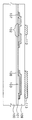
도 4는 도 2의 A-A'선에 따른 유기전계발광 표시장치의 단면도이다.4 is a cross-sectional view of an organic light emitting display device taken along the line AA ′ of FIG. 2.
도 5a 내지 도 5e는 도 4에 도시한 유기전계발광 표시장치의 제조방법을 설명하기 위한 단면도들이다.5A through 5E are cross-sectional views illustrating a method of manufacturing the organic light emitting display device illustrated in FIG. 4.
<도면의 주요 부분에 대한 부호의 설명〉<Explanation of symbols for main parts of the drawings>
100 : 기판 101 : 차단막100
102, 103 : 버퍼층 105, 106, 107 : 액티브 패턴102, 103:
108 : 제1 전극 109 : 게이트 절연막108: first electrode 109: gate insulating film
110, 111, 112 : 게이트 전극 113 : 제2 전극110, 111, 112: gate electrode 113: second electrode
114 : 층간 절연막 115, 116, 117, 118, 119, 120 : 콘택홀
114: interlayer
122, 125, 127 : 소오스 전극 123, 124, 126 : 드레인 전극122, 125, 127:
128 : 제3 전극 130 : 보호막128: third electrode 130: protective film
132 : 비어홀 134 : 화소 전극132: via hole 134: pixel electrode
135 : 제4 전극 136 : 유기 절연막135: fourth electrode 136: organic insulating film
137 : 개구부 138 : 정공 수송층137: opening 138: hole transport layer
140 : 발광층 142 : 전자 수송층140: light emitting layer 142: electron transport layer
144 : 음극 전극 EL : 유기전계발광 소자144: cathode electrode EL: organic electroluminescent element
GL1, GL2 : 게이트 라인 DL : 데이터 라인GL1, GL2: Gate Line DL: Data Line
T1, T2, T3 : 박막 트랜지스터 C1, C2 : 캐패시터T1, T2, T3: thin film transistors C1, C2: capacitor
본 발명은 액티브 매트릭스형 유기전계발광 표시장치 및 그 제조방법에 관한 것으로, 보다 상세하게는 화소당 두 개 이상의 캐패시터를 필요로 하는 보상 회로들을 적용할 때 개구율 저하를 방지할 수 있는 액티브 매트릭스형 유기전계발광 표시장치 및 그 제조방법에 관한 것이다.BACKGROUND OF THE
오늘날과 같은 정보화 사회에 있어서 전자 디스플레이 장치(electronic display device)의 역할은 갈수록 중요해지며, 각종 전자 디스플레이 장치가 다양한 산업 분야에 광범위하게 사용되고 있다.In today's information society, the role of electronic display devices becomes more and more important, and various electronic display devices are widely used in various industrial fields.
일반적으로 전자 디스플레이 장치란 다양한 정보를 시각을 통해 인간에게 전 달하는 장치를 말한다. 즉, 전자 디스플레이 장치란 각종 전자 기기로부터 출력되는 전기적 정보 신호를 인간의 시각으로 인식 가능한 광 정보 신호로 변환하는 전자 장치라고 정의할 수 있으며, 인간과 전자 기기를 연결하는 가교적 역할을 담당하는 장치로 정의될 수도 있다.In general, an electronic display device refers to a device that transmits various information to a human through vision. That is, an electronic display device may be defined as an electronic device that converts electrical information signals output from various electronic devices into optical information signals that can be recognized by a human vision, and plays a role of a bridge between humans and electronic devices. It may be defined as.
이러한 전자 디스플레이 장치에 있어서, 광 정보 신호가 발광 현상에 의해 표시되는 경우에는 발광형 표시(emissive display) 장치로 불려지며, 반사, 산란, 간섭 현상 등에 의해 광 변조를 표시되는 경우에는 수광형 표시(non-emissive display) 장치로 일컬어진다. 능동형 표시 장치라고도 불리는 상기 발광형 표시 장치로는 음극선관(cathode ray tube; CRT), 플라즈마 디스플레이 패널(plasma display panel; PDP), 발광 다이오드(light emitting diode; LED) 및 일렉트로 루미네슨트 디스플레이(electroluminescent display; ELD) 등을 들 수 있다. 또한, 수동형 표시 장치인 상기 수광형 표시 장치에는 액정표시장치(liquid crystal display; LCD), 전기화학 표시장치(electrochemical display; ECD) 및 전기 영동 표시장치(electrophoretic image display; EPID) 등이 해당된다.In such an electronic display device, when an optical information signal is displayed by a light emitting phenomenon, it is called an emissive display device, and when a light modulation is displayed by reflection, scattering, or interference phenomenon, a light receiving display ( It is called a non-emissive display device. The light emitting display device, also called an active display device, includes a cathode ray tube (CRT), a plasma display panel (PDP), a light emitting diode (LED), and an electroluminescent display (electroluminescent display). display; ELD). In addition, the light receiving display device, which is a passive display device, includes a liquid crystal display (LCD), an electrochemical display (ECD), an electrophoretic image display (EPID), and the like.
텔레비전이나 컴퓨터용 모니터 등과 같은 화상표시장치에 사용되는 음극선관(CRT)은 표시 품질 및 경제성 등의 면에서 가장 높은 점유율을 차지하고 있으나, 무거운 중량, 큰 용적 및 높은 소비 전력 등과 같은 많은 단점을 가지고 있다.Cathode ray tubes (CRTs) used in image display devices such as televisions and computer monitors occupy the highest share in terms of display quality and economy, but have many disadvantages such as heavy weight, large volume and high power consumption. .
그러나, 반도체 기술의 급속한 진보에 의해 각종 전자 장치의 고체화, 저 전압 및 저 전력화와 함께 전자 기기의 소형 및 경량화에 따라 새로운 환경에 적합한 전자 디스플레이 장치, 즉 얇고 가벼우면서도 낮은 구동 전압 및 낮은 소비 전력의 특징을 갖춘 평판(flat panel) 디스플레이 장치에 대한 요구가 급격히 증대하고 있다.However, due to the rapid progress of semiconductor technology, the electronic display device suitable for the new environment, that is, the thin and light, the low driving voltage and the low power consumption of the electronic device, according to the miniaturization, low voltage and low power of various electronic devices, and the miniaturization and light weight of electronic devices The demand for flat panel display devices with features is rapidly increasing.
이러한 평판 디스플레이 장치의 하나로서 전계발광 소자가 주목되고 있다. 전계발광 소자는 사용하는 재료에 따라 무기전계발광 소자와 유기전계발광 소자로 크게 나뉘어진다.As one of such flat panel display apparatuses, an electroluminescent element is attracting attention. Electroluminescent devices are broadly classified into inorganic electroluminescent devices and organic electroluminescent devices according to materials used.
무기전계발광 소자는 일반적으로 발광부에 높은 전계를 인가하고 전자를 높은 전계 중에서 가속하여 발광 중심으로 충돌시켜 이에 의해 발광 중심을 여기 함으로써 발광하는 소자이다.In general, an inorganic electroluminescent device is a device that emits light by applying a high electric field to a light emitting part and accelerating electrons in a high electric field to impinge on the light emitting center, thereby exciting the light emitting center.
유기전계발광 소자는 음극(cathode) 전극과 양극(anode) 전극으로부터 각각 전자(electron)와 정공(hole)을 발광부 내로 주입시켜 주입된 전자와 정공이 결합하여 여기자(exciton)를 생성하고, 이 여기자가 여기상태로부터 기저상태로 떨어질 때 발광하는 소자이다.The organic electroluminescent device injects electrons and holes from the cathode electrode and the anode electrode into the light emitting unit, respectively, and combines the injected electrons and holes to generate excitons. It is an element that emits light when the excitons fall from the excited state to the ground state.
상기와 같은 동작원리로 인해 무기전계발광 소자는 100∼200V의 높은 구동전압을 필요로 하는 반면, 유기전계발광 소자는 5∼20V정도의 낮은 전압으로 구동할 수 있다는 장점 때문에 이에 대한 연구가 더욱 활발하게 진행되고 있다. 또한, 유기전계발광 소자는 넓은 시야각, 고속 응답성, 고 콘트라스트(high contrast) 등의 우수한 특징을 갖고 있다.Due to the above operation principle, the inorganic electroluminescent device needs a high driving voltage of 100 to 200V, while the organic electroluminescent device can be driven at a low voltage of about 5 to 20V. Is going on. In addition, the organic light emitting display device has excellent characteristics such as wide viewing angle, high speed response, and high contrast.
유기전계발광 소자는 액티브 매트릭스형 디스플레이 장치와 패시브 매트릭스형 디스플레이 장치에 모두 적용할 수 있다. 액티브 매트릭스형 유기전계발광 표시 장치는 박막 트랜지스터와 같은 스위칭 소자들에 의해 복수개의 화소들에 대응하는 유기전계발광 소자들을 서로 독립적으로 구동시키는 디스플레이 장치이다.The organic light emitting display device can be applied to both an active matrix display device and a passive matrix display device. The active matrix type organic light emitting display device is a display device that independently drives organic light emitting display elements corresponding to a plurality of pixels by switching elements such as thin film transistors.
도 1은 종래의 액티브 매트릭스형 유기전계발광 표시장치의 등가 회로도이다.1 is an equivalent circuit diagram of a conventional active matrix organic light emitting display device.
도 1을 참조하면, 종래의 액티브 매트릭스형 유기전계발광 표시장치의 화소 회로는 두 개의 박막 트랜지스터(TFT1, TFT2)와 한 개의 캐패시터(Cst)로 구성된다.Referring to FIG. 1, a pixel circuit of a conventional active matrix organic light emitting display device includes two thin film transistors TFT1 and TFT2 and one capacitor Cst.
구체적으로, 복수개의 게이트 라인(g1, g2)과 복수개의 데이터 라인(d1, d2)이 교차 배열되어 단위 화소 영역을 한정한다. 인접한 데이터 라인(d1, d2)들 사이에는 직류 신호 라인(Vdd)이 상기 데이터 라인(d1, d2)과 평행하게 배열된다. 직류 신호 라인(Vdd)에는 디스플레이 신호의 최대 값이 직류 상태로 인가된다.In detail, the plurality of gate lines g1 and g2 and the plurality of data lines d1 and d2 are alternately arranged to define a unit pixel area. The DC signal line Vdd is arranged in parallel with the data lines d1 and d2 between the adjacent data lines d1 and d2. The maximum value of the display signal is applied to the DC signal line Vdd in a DC state.
게이트 라인(g1)과 데이터 라인(d1)의 교차점에는 스위칭 소자인 제1 박막 트랜지스터(TFT1)가 연결된다. 제1 박막 트랜지스터(TFT1)의 게이트 전극은 게이트 라인(g1)과 연결되고, 소오스 전극은 데이터 라인(d1)과 연결된다.The first thin film transistor TFT1, which is a switching element, is connected to the intersection of the gate line g1 and the data line d1. The gate electrode of the first thin film transistor TFT1 is connected to the gate line g1, and the source electrode is connected to the data line d1.
제1 박막 트랜지스터(TFT1)의 드레인 전극과 직류 신호 라인(Vdd) 사이에는 스토리지 캐패시터(Cst)가 연결된다. 또한, 제1 박막 트랜지스터(TFT1)의 드레인 전극과 직류 신호 라인(Vdd) 사이에는 상기 스토리지 캐패시터(Cst)와 병렬로 구동 소자인 제2 박막 트랜지스터(TFT2)가 연결된다. 상기 제2 박막 트랜지스터(T2)의 게이트 전극은 제1 박막 트랜지스터(TFT1)의 드레인 전극과 연결되고, 소오스 전극은 직류 신호 라인(Vdd)과 연결되며, 드레인 전극은 유기전계발광 소자(EL)에 연결 된다.The storage capacitor Cst is connected between the drain electrode of the first thin film transistor TFT1 and the DC signal line Vdd. In addition, a second thin film transistor TFT2, which is a driving element, is connected in parallel with the storage capacitor Cst between the drain electrode of the first thin film transistor TFT1 and the DC signal line Vdd. The gate electrode of the second thin film transistor T2 is connected to the drain electrode of the first thin film transistor TFT1, the source electrode is connected to the DC signal line Vdd, and the drain electrode is connected to the organic light emitting diode EL. Is connected.
상기 제1 박막 트랜지스터(TFT1)가 턴온(turn-on)되면 데이터 라인(d1)의 디스플레이 신호 값에 따라 제2 박막 트랜지스터(TFT2)가 턴온되고, 직류 신호 라인(Vdd)의 직류 신호 값이 유기전계발광 소자(EL)에 인가되어 유기전계발광 소자(EL)가 구동된다.When the first thin film transistor TFT1 is turned on, the second thin film transistor TFT2 is turned on according to the display signal value of the data line d1, and the direct current signal value of the DC signal line Vdd is organic. The organic electroluminescent element EL is driven by being applied to the electroluminescent element EL.
그러나, 이와 같이 두 개의 박막 트랜지스터를 사용하는 회로를 적용한 유기전계발광 표시장치에 의하면, 구동 박막 트랜지스터의 특성 편차, 예를 들어 문턱 전압(threshold voltage)의 변동(variation) 등에 의해 패널 상의 휘도가 균일하지 못하는 문제가 발생한다.However, according to the organic light emitting display device employing the circuit using two thin film transistors as described above, the luminance on the panel is uniform due to the characteristic variation of the driving thin film transistor, for example, the variation of the threshold voltage. The problem does not occur.
이에 따라, 구동 박막 트랜지스터의 특성 편차를 보상하기 위하여 별도의 박막 트랜지스터를 추가하는 보상 회로들이 제안되었다. 그러나, 이러한 보상 회로를 적용할 경우 박막 트랜지스터의 개수가 증가하기 때문에, 단위 화소 영역에 박막 트랜지스터가 차지하는 면적이 증가하여 개구율이 저하된다. 또한, 보상 회로들 중에서 일부 회로는 화소당 서로 다른 기능을 갖는 두 개의 캐패시터를 필요로 하게 되므로, 단위 화소에 배치되는 박막 트랜지스터와 캐패시터 개수의 증가로 인하여 개구율이 상당히 감소된다. 이러한 개구율의 감소는 휘도의 저하를 초래하고, 고전류 구동을 요구하여 수명이 감소되는 결과를 가져온다.Accordingly, compensation circuits have been proposed in which an additional thin film transistor is added to compensate for the characteristic variation of the driving thin film transistor. However, when the compensation circuit is applied, the number of the thin film transistors increases, so that the area occupied by the thin film transistors in the unit pixel area increases, thereby decreasing the aperture ratio. In addition, some of the compensation circuits require two capacitors having different functions per pixel, so that the aperture ratio is considerably reduced due to the increase in the number of thin film transistors and capacitors disposed in the unit pixel. This reduction in aperture ratio results in a decrease in luminance and requires high current driving, resulting in a reduction in lifetime.
따라서, 본 발명의 일 목적은 화소당 두 개 이상의 캐패시터를 필요로 하는 보상 회로를 적용할 때 개구율 저하를 방지할 수 있는 액티브 매트릭스형 유기전계 발광 표시장치를 제공하는데 있다.Accordingly, an object of the present invention is to provide an active matrix type organic light emitting display device which can prevent a decrease in aperture ratio when applying a compensation circuit requiring two or more capacitors per pixel.
본 발명의 일 목적은 화소당 두 개 이상의 캐패시터를 필요로 하는 보상 회로를 적용하는 액티브 매트릭스형 유기전계발광 표시장치의 개구율 저하를 방지할 수 있는 액티브 매트릭스형 유기전계발광 표시장치의 제조방법을 제공하는데 있다.SUMMARY OF THE INVENTION An object of the present invention is to provide a method of manufacturing an active matrix organic light emitting display device capable of preventing the aperture ratio of an active matrix type organic light emitting display device applying a compensation circuit requiring two or more capacitors per pixel. It is.
상술한 본 발명의 일 목적을 달성하기 위하여 본 발명은, 단위 화소 영역 내에 서로 다른 기능을 갖는 적어도 두 개의 캐패시터가 배치되고, 상기 적어도 두 개의 캐패시터는 수직 방향으로 적층되어 형성된 것을 특징으로 하는 액티브 매트릭스형 유기전계발광 표시장치를 제공한다.In order to achieve the above object of the present invention, in the present invention, at least two capacitors having different functions are disposed in a unit pixel area, and the at least two capacitors are formed by being stacked in a vertical direction. It provides a type organic light emitting display device.
또한, 본 발명의 상술한 일 목적은, 제1 방향으로 신장되는 제1 및 제2 게이트 라인과, 상기 제1 방향과 직교하는 제2 방향으로 신장되는 데이터 라인 및 직류 신호 라인에 의해 단위 화소가 한정되는 액티브 매트릭스형 유기전계발광 표시장치에 있어서, 상기 제1 게이트 라인에 제1 게이트 전극이 연결되고, 상기 데이터 라인에 제1 소오스 전극이 연결된 제1 박막 트랜지스터; 상기 제2 게이트 라인에 제2 게이트 전극이 연결된 제2 박막 트랜지스터; 상기 직류 신호 라인에 제3 소오스 전극이 연결된 제3 박막 트랜지스터; 상기 제3 박막 트랜지스터의 제3 드레인 전극과 접지단 사이에 연결된 유기전계발광 소자; 상기 제3 박막 트랜지스터의 제3 게이트 전극 및 상기 제2 박막 트랜지스터의 제2 소오스 전극에 연결된 제1 전극과, 상기 제1 박막 트랜지스터의 제1 드레인 전극에 연결된 제2 전극을 포함하는 제1 캐패시터; 및 상기 제2 전극과 상기 직류 신호 라인에 연결된 제3 전극을 포함하는 제2 캐패시터를 구비하며, 상기 제1 및 제2 캐패시터는 서로 다른 기능을 가지며 수직 방향으로 적층되어 형성된 것을 특징으로 하는 액티브 매트릭스형 유기전계발광 표시장치에 의해 달성될 수 있다.In addition, one object of the present invention is that a unit pixel is formed by first and second gate lines extending in a first direction, and data lines and direct current signal lines extending in a second direction orthogonal to the first direction. An active matrix type organic light emitting display device, comprising: a first thin film transistor having a first gate electrode connected to the first gate line and a first source electrode connected to the data line; A second thin film transistor having a second gate electrode connected to the second gate line; A third thin film transistor having a third source electrode connected to the DC signal line; An organic light emitting diode connected between the third drain electrode and the ground terminal of the third thin film transistor; A first capacitor including a first electrode connected to a third gate electrode of the third thin film transistor and a second source electrode of the second thin film transistor, and a second electrode connected to a first drain electrode of the first thin film transistor; And a second capacitor including a second electrode and a third electrode connected to the DC signal line, wherein the first and second capacitors have different functions and are stacked in a vertical direction. It can be achieved by a type organic light emitting display device.
또한, 상술한 본 발명의 일 목적을 달성하기 위하여 본 발명은, 제1 방향으로 신장되는 제1 및 제2 게이트 라인과, 상기 제1 방향과 직교하는 제2 방향으로 신장되는 데이터 라인 및 직류 신호 라인에 의해 단위 화소가 한정되는 액티브 매트릭스형 유기전계발광 표시장치에 있어서, 상기 제1 게이트 라인과 데이터 라인의 교차점 부근에 배치된 제1 액티브 패턴, 상기 제1 게이트 라인으로부터 연장되어 상기 제1 액티브 패턴 위를 지나가는 제1 게이트 전극, 상기 데이터 라인으로부터 연장되어 상기 제1 게이트 전극 일측의 제1 액티브 패턴과 콘택되는 제1 소오스 전극 및 상기 제1 게이트 전극 타측의 제1 액티브 패턴과 콘택되는 제1 드레인 전극을 포함하는 제1 박막 트랜지스터; 상기 제2 게이트 라인과 데이터 라인의 교차점 부근에 배치된 제2 액티브 패턴, 상기 제2 게이트 라인으로부터 연장되어 상기 제2 액티브 패턴 위를 지나가는 제2 게이트 전극, 상기 제2 게이트 전극 일측의 제2 액티브 패턴과 콘택되는 제2 소오스 전극 및 상기 제2 게이트 전극 타측의 제2 액티브 패턴과 콘택되는 제2 드레인 전극을 포함하는 제2 박막 트랜지스터; 상기 단위 화소 내에 배치된 제3 액티브 패턴, 상기 제3 액티브 패턴 위를 지나가는 제3 게이트 전극, 상기 직류 신호 라인으로부터 연장되어 상기 제3 게이트 전극 일측의 제3 액티브 패턴과 콘택되는 제3 소오스 전극 및 상기 제2 드레인 전극으로부터 연장되어 상기 제3 게이트 전극 타측의 제3 액티브 패턴과 콘택되는 제3 드레인 전극을 포함하는 제3 박막 트랜지스터; 상기 제2 액티브 패턴으로부터 연장되고 상기 직류 신호 라인의 하부에 상기 직류 신호 라인과 평행하게 배치된 제1 전극 및 상기 제1 전극 상에 형성되고 상기 제1 드레인 전극과 연결되는 제2 전극을 포함하는 제1 캐패시터; 상기 제2 전극 및 상기 제2 전극 상에 형성되고 상기 직류 신호 라인으로 이루어진 제3 전극을 포함하며, 상기 제1 캐패시터와는 서로 다른 기능을 갖는 제2 캐패시터; 및 상기 제3 드레인 전극과 콘택되어 상기 단위 화소 내에 배치된 화소 전극을 구비하는 것을 특징으로 하는 액티브 매트릭스형 유기전계발광 표시장치를 제공한다.In addition, in order to achieve the above object of the present invention, the present invention, the first and second gate line extending in the first direction, the data line and DC signal extending in the second direction orthogonal to the first direction An active matrix type organic light emitting display device in which a unit pixel is defined by a line, comprising: a first active pattern disposed near an intersection point of the first gate line and a data line and extending from the first gate line; A first gate electrode passing over the pattern, a first source electrode extending from the data line and contacting the first active pattern on one side of the first gate electrode, and a first active pattern on the other side of the first gate electrode A first thin film transistor including a drain electrode; A second active pattern disposed near an intersection point of the second gate line and the data line, a second gate electrode extending from the second gate line and passing over the second active pattern, and a second active pattern on one side of the second gate electrode A second thin film transistor including a second source electrode in contact with a pattern and a second drain electrode in contact with a second active pattern on the other side of the second gate electrode; A third active pattern disposed in the unit pixel, a third gate electrode passing over the third active pattern, a third source electrode extending from the DC signal line and contacting a third active pattern on one side of the third gate electrode; A third thin film transistor extending from the second drain electrode and including a third drain electrode contacting a third active pattern on the other side of the third gate electrode; A first electrode extending from the second active pattern and disposed under the DC signal line in parallel with the DC signal line, and a second electrode formed on the first electrode and connected to the first drain electrode; A first capacitor; A second capacitor formed on the second electrode and the second electrode and including a third electrode formed of the DC signal line, the second capacitor having a function different from that of the first capacitor; And a pixel electrode in contact with the third drain electrode and disposed in the unit pixel.
상술한 본 발명의 다른 목적을 달성하기 위하여 본 발명은, 기판 상의 각 화소 영역에 액티브 패턴들 및 제1 전극을 형성하는 단계; 상기 액티브 패턴, 제1 전극 및 기판 상에 게이트 절연막을 형성하는 단계; 상기 액티브 패턴 위의 게이트 절연막 상에 제1, 제2 및 제3 게이트 전극을 형성하고 상기 제1 전극 위의 게이트 절연막 상에 제2 전극을 형성하여 상기 제1 전극, 게이트 절연막 및 제2 전극으로 이루어진 제1 캐패시터를 형성하는 단계; 상기 제1, 제2 및 제3 게이트 전극, 제2 전극 및 게이트 절연막 상에 층간 절연막을 형성하는 단계; 상기 액티브 패턴들 위의 층간 절연막 상에 제1, 제2 및 제3 소오스 전극과 제1, 제2 및 드레인 전극을 형성하여 제1 게이트 전극, 제1 소오스 전극 및 제1 드레인 전극을 포함하는 제1 박막 트랜지스터, 제2 게이트 전극, 제2 소오스 전극 및 제2 드레인 전극을 포함하는 제2 박막 트랜지스터 및 제3 게이트 전극, 제3 소오스 전극 및 제3 드레인 전극을 포함하는 제1 박막 트랜지스터를 형성함과 동시에, 상기 제1 전극 위의 층간 절 연막 상에 제3 전극을 형성하여 상기 제1 캐패시터 상에 수직으로 적층되고 제2 전극, 층간 절연막 및 제3 전극으로 이루어진 제2 캐패시터를 형성하는 단계; 상기 제1, 제2 및 제3 박막 트랜지스터, 제1 및 제2 캐패시터와 층간 절연막 상에 보호막을 형성하는 단계; 상기 보호막 상에 화소 전극을 형성하는 단계; 및 상기 화소 전극 상에 유기전계발광 소자를 형성하는 단계를 구비하는 것을 특징으로 하는 액티브 매트릭스형 유기전계발광 표시장치의 제조방법을 제공한다.In order to achieve the above object of the present invention, the present invention comprises the steps of forming an active pattern and a first electrode in each pixel area on the substrate; Forming a gate insulating film on the active pattern, the first electrode and the substrate; First, second and third gate electrodes are formed on the gate insulating layer on the active pattern, and a second electrode is formed on the gate insulating layer on the first electrode to form the first electrode, the gate insulating layer, and the second electrode. Forming a first capacitor; Forming an interlayer insulating film on the first, second and third gate electrodes, the second electrode and the gate insulating film; First, second, and third source electrodes and first, second, and drain electrodes formed on the interlayer insulating layer over the active patterns to include a first gate electrode, a first source electrode, and a first drain electrode; Forming a second thin film transistor including a first thin film transistor, a second gate electrode, a second source electrode, and a second drain electrode and a first thin film transistor including a third gate electrode, a third source electrode, and a third drain electrode And simultaneously forming a third electrode on the interlayer insulating film on the first electrode to form a second capacitor vertically stacked on the first capacitor and comprising a second electrode, an interlayer insulating film, and a third electrode; Forming a protective film on the first, second and third thin film transistors, the first and second capacitors, and an interlayer insulating film; Forming a pixel electrode on the passivation layer; And forming an organic light emitting display device on the pixel electrode.
본 발명에 의하면, 화소당 서로 다른 기능을 갖는 두 개 이상의 캐패시터를 필요로 하는 보상 회로를 적용할 때 상기 두 개 이상의 캐패시터를 수직 방향으로 적층시킴으로써, 화소 내 캐패시터 개수의 증가에 따른 개구율 저하를 방지할 수 있다.According to the present invention, when applying a compensation circuit requiring two or more capacitors having different functions per pixel, the two or more capacitors are stacked in a vertical direction, thereby preventing a decrease in aperture ratio due to an increase in the number of capacitors in a pixel. can do.
이하, 첨부한 도면을 참조하여 본 발명의 바람직한 실시예를 상세히 설명하고자 한다.Hereinafter, exemplary embodiments of the present invention will be described in detail with reference to the accompanying drawings.
도 2는 본 발명에 의한 액티브 매트릭스형 유기전계발광 표시장치의 평면도이다. 도 3은 도 2에 도시한 액티브 매트릭스형 유기전계발광 표시장치의 등가 회로도이다. 도 4는 도 2의 A-A'선에 따른 유기전계발광 표시장치의 단면도이다.2 is a plan view of an active matrix organic light emitting display device according to the present invention. FIG. 3 is an equivalent circuit diagram of the active matrix organic light emitting display device shown in FIG. 2. 4 is a cross-sectional view of an organic light emitting display device taken along the line AA ′ of FIG. 2.
도 2 내지 도 4를 참조하면, 본 발명의 액티브 매트릭스형 유기전계발광 표시장치의 화소 회로는 세 개의 박막 트랜지스터(T1, T2, T3)와 두 개의 캐패시터(C1, C2), 그리고 네 개의 배선(GL1, GL2, DL, Vdd)으로 구성된다.2 to 4, the pixel circuit of the active matrix organic light emitting display device according to the present invention includes three thin film transistors T1, T2, and T3, two capacitors C1 and C2, and four wirings ( GL1, GL2, DL, Vdd).
구체적으로, 제1 방향으로 신장되는 제1 및 제2 게이트 라인(GL1, GL2)과, 상기 제1 방향과 직교하는 제2 방향으로 신장되는 데이터 라인(DL) 및 직류 신호 라인(Vdd)에 의해 단위 화소가 한정된다.Specifically, the first and second gate lines GL1 and GL2 extend in the first direction, and the data line DL and the DC signal line Vdd extend in the second direction orthogonal to the first direction. The unit pixel is limited.
상기 제1 게이트 라인(GL1)은 스위칭 소자인 제1 박막 트랜지스터(T1)를 온/오프하여 데이터 라인(DL)을 통해 초기 데이터 전압 및 계조 데이터 전압을 인가하는 역할을 한다. 상기 제2 게이트 라인(GL2)은 제2 박막 트랜지스터(T2)를 온/오프하여 구동 소자인 제3 박막 트랜지스터(T3)의 특성을 보상하는 역할을 한다. 상기 직류 신호 라인(Vdd)에는 디스플레이 신호의 최대 값이 직류 상태로 일정하게 인가된다.The first gate line GL1 turns on / off the first thin film transistor T1, which is a switching element, and applies an initial data voltage and a gray data voltage through the data line DL. The second gate line GL2 turns on / off the second thin film transistor T2 to compensate for the characteristics of the third thin film transistor T3 as a driving element. The maximum value of the display signal is constantly applied to the DC signal line Vdd in a DC state.
상기 제1 박막 트랜지스터(T1)는 제1 게이트 라인(GL1)과 데이터 라인(DL)의 교차점 부근에 배치된 제1 액티브 패턴(105), 제1 게이트 라인(GL1)으로부터 연장되어 제1 액티브 패턴(105) 위를 지나가는 제1 게이트 전극(110), 데이터 라인(DL)으로부터 연장되어 제1 게이트 전극(110) 일측의 제1 액티브 패턴(105)과 콘택되는 제1 소오스 전극(122) 및 제1 게이트 전극(110) 타측의 제1 액티브 패턴(105)과 콘택되는 제1 드레인 전극(123)을 포함한다. 제1 박막 트랜지스터(T1)의 제1 게이트 전극(110)은 제1 게이트 라인(GL1)과 연결되고, 제1 소오스 전극(122)은 데이터 라인(d1)과 연결된다.The first thin film transistor T1 extends from the first
상기 제2 박막 트랜지스터(T2)는 제2 게이트 라인(GL2)과 데이터 라인(DL)의 교차점 부근에 배치된 제2 액티브 패턴(106), 제2 게이트 라인(GL2)으로부터 연장되어 제2 액티브 패턴(106) 위를 지나가는 제2 게이트 전극(111), 제2 게이트 전극(111) 일측의 제2 액티브 패턴(106)과 콘택되는 제2 소오스 전극(125) 및 제2 게이트 전극(111) 타측의 제2 액티브 패턴(106)과 콘택되는 제2 드레인 전극(124) 을 포함한다. 제2 박막 트랜지스터(T2)의 제2 게이트 전극(111)은 제2 게이트 라인(GL2)과 연결된다.The second thin film transistor T2 extends from the second
상기 제3 박막 트랜지스터(T3)는 단위 화소 내에 배치된 제3 액티브 패턴(107), 제3 액티브 패턴(107) 위를 지나가는 제3 게이트 전극(112), 직류 신호 라인(Vdd)으로부터 연장되어 제3 게이트 전극(112) 일측의 제3 액티브 패턴(107)과 콘택되는 제3 소오스 전극(127) 및 제2 드레인 전극(124)으로부터 연장되어 제3 게이트 전극(112) 타측의 제3 액티브 패턴(107)과 콘택되는 제3 드레인 전극(126)을 포함한다. 상기 제3 박막 트랜지스터(T3)의 제3 게이트 전극(112)은 제2 박막 트랜지스터(T2)의 제2 소오스 전극(125)과 연결되고, 제3 소오스 전극(127)은 직류 신호 라인(Vdd)과 연결되며, 제3 드레인 전극(126)은 제2 박막 트랜지스터(T2)의 제2 드레인 전극(124) 및 유기전계발광 소자(EL)와 연결된다.The third thin film transistor T3 extends from the third
바람직하게는, 상기 제3 박막 트랜지스터(T3)는 p형으로 형성되고, 제1 및 제2 박막 트랜지스터(T1, T2)는 n형 또는 p형 중의 하나로 형성한다.Preferably, the third thin film transistor T3 is formed in a p type, and the first and second thin film transistors T1 and T2 are formed in one of an n type or a p type.
상기 제1 캐패시터(C1)는 제2 박막 트랜지스터(T2)의 제2 액티브 패턴(106)으로부터 연장되고 직류 신호 라인(Vdd)의 하부에 상기 직류 신호 라인(Vdd)과 평행하게 배치된 제1 전극(108), 게이트 절연막(109) 및 제1 전극(108)과 오버랩되는 제2 전극(113)으로 구성된다. 상기 제1 전극(108)은 제1, 제2 및 제3 박막 트랜지스터(T1, T2, T3)의 액티브 패턴들(105, 106, 107)과 동일한 층으로 형성된다. 상기 제2 전극(113)은 게이트 라인(GL)과 동일한 층으로 형성된다. 제1 캐패시터(C1)의 제1 전극(108)은 제3 박막 트랜지스터(T3)의 제3 게이트 전극(112) 및 제2 박막 트랜지스터(T2)의 제2 소오스 전극(125)에 연결되고, 제2 전극(113)은 제1 박막 트랜지스터(T1)의 제1 드레인 전극(123)에 연결된다. 상기 제1 캐패시터(C1)는 제3 박막 트랜지스터(T3)의 특성이 보상된 전압을 저장하고, 커플링(coupling)을 통해 제3 박막 트랜지스터(T3)의 제3 게이트 전극(112)에 데이터 전압을 전달하는 역할을 한다.The first capacitor C1 extends from the second
상기 제2 캐패시터(C2)는 상기 제2 전극(113), 층간 절연막(114) 및 제2 전극(113)과 오버랩되는 제3 전극(128)으로 구성된다. 제2 캐패시터(C2)의 제3 전극(128)은 직류 신호 라인(Vdd)에 연결된다. 상기 제3 전극(128)은 데이터 라인(DL)과 동일한 층으로 형성된다. 상기 제2 캐패시터(C2)는 직류 신호 라인(Vdd)과 제1 박막 트랜지스터(T1)의 제1 드레인 전극(123) 사이에 연결되며, 프레임 시간 동안 데이터 전압을 일정하게 유지시키는 역할을 한다.The second capacitor C2 includes the
따라서, 제1 캐패시터(C1)와 제2 캐패시터(C2)는 다른 기능을 가지며, 제1 박막 트랜지스터(T1)의 제1 드레인 전극(123)에 연결된 공통 전극, 즉 제2 전극(113)을 공유하여 수직 방향으로 적층되어 형성된다.Accordingly, the first capacitor C1 and the second capacitor C2 have different functions, and share the common electrode, that is, the
본 발명의 단위 화소 영역 내에는 제3 박막 트랜지스터(T3)의 제3 드레인 전극(126)과 콘택되는 화소 전극(134)이 형성된다. 또한, 상기 화소 전극(134)과 동일한 층으로 이루어진 제4 전극(135)이 제2 캐패시터(C2)의 제3 전극(128)과 오버랩되도록 형성된다. 만일 제2 캐패시터(C2)에 높은 캐패시턴스가 요구된다면, 상기 제2 전극(113)과 제4 전극(135) 사이의 존재하는 층간 절연막(114) 및 보호막(130)으로 유전막을 구성함으로써 캐패시턴스를 확보할 수 있다.
The
본 발명에 의한 화소 회로는 다음과 같이 구동된다.The pixel circuit according to the present invention is driven as follows.
즉, 상기 제1 게이트 라인(GL1)에 의해 제1 박막 트랜지스터(T1)가 턴온되면, 데이터 라인(DL)의 디스플레이 신호 값에 따라 제3 박막 트랜지스터(T3)가 턴온되고, 직류 신호 라인(Vdd)의 직류 신호 값이 유기전계발광 소자(EL)에 인가되어 유기전계발광 소자(EL)가 구동된다. 이때, 제2 게이트 라인(GL2)에 보상 전압을 인가하여 제2 박막 트랜지스터(T2)를 턴온시키면, 제3 박막 트랜지스터(T3)의 제3 게이트 전극(112)과 제3 드레인 전극(126)이 연결되어 구동 소자인 제3 박막 트랜지스터(T3)의 특성 차이가 줄어들게 된다.That is, when the first thin film transistor T1 is turned on by the first gate line GL1, the third thin film transistor T3 is turned on according to the display signal value of the data line DL, and the DC signal line Vdd is turned on. Value of the direct current signal is applied to the organic light emitting diode EL to drive the organic light emitting diode EL. In this case, when the second thin film transistor T2 is turned on by applying a compensation voltage to the second gate line GL2, the
이하, 상술한 구조를 갖는 본 발명의 액티브 매트릭스형 유기전계발광 표시장치의 제조방법을 설명하고자 한다.Hereinafter, a method of manufacturing an active matrix organic light emitting display device having the above-described structure will be described.
도 5a 내지 도 5e는 도 4에 도시한 유기전계발광 표시장치의 제조방법을 설명하기 위한 단면도들이다.5A through 5E are cross-sectional views illustrating a method of manufacturing the organic light emitting display device illustrated in FIG. 4.
도 5a를 참조하면, 유리, 석영, 사파이어와 같은 절연 기판(100) 상에 실리콘 산화물을 플라즈마-증대 화학기상증착(plasma-enhanced chemical vapor deposition; PECVD) 방법에 의해 약 2000Å의 두께로 증착하여 차단막(blocking layer)(101)을 형성한다. 상기 차단막(101)은 후속의 비정질실리콘막의 결정화 동안에 열손실을 방지하기 위하여 사용하는 것이 바람직하다.Referring to FIG. 5A, a silicon oxide is deposited on an insulating
상기 차단막(101) 상에 n형 불순물로 도핑된 비정질실리콘막을 PECVD 방법에 의해 약 800Å의 두께로 증착한 후, 이를 사진식각 공정으로 패터닝하여 단위 화소 내의 박막 트랜지스터 영역 및 캐패시터 영역에 버퍼층(102, 103)을 형성한다.
An amorphous silicon film doped with n-type impurities on the
이어서, 상기 버퍼층(102, 103) 및 차단막(101) 상에 비정질실리콘막을 저압 화학 기상 증착(low pressure CVD; LPCVD) 또는 PECVD 방법에 의해 약 500Å의 두께로 증착하여 액티브층(104)을 형성한 후, 레이저 어닐링 또는 퍼니스 어닐링(furnace annealing)을 실시하여 상기 액티브층(104)을 다결정실리콘으로 결정화시킨다.Subsequently, an amorphous silicon film is deposited on the buffer layers 102 and 103 and the blocking
도 5b를 참조하면, 사진식각 공정으로 상기 다결정실리콘 액티브층(104)을 패터닝하여 단위 화소 내의 박막 트랜지스터 영역에 제1 액티브 패턴(도 2의 105), 제2 액티브 패턴(도 2의 106) 및 제3 액티브 패턴(107)을 형성한다. 이와 동시에, 단위 화소 내의 캐패시터 영역에 상기 다결정실리콘 액티브층으로 이루어진 제1 전극(108)을 형성한다.Referring to FIG. 5B, the polysilicon
이어서, 상기 액티브 패턴들(105, 106, 107) 및 제1 전극(108)이 형성된 결과물의 전면에 실리콘 산화물을 PECVD 방법에 의해 1000Å∼2000Å의 두께로 증착하여 게이트 절연막(109)을 형성한다.Subsequently, silicon oxide is deposited on the entire surface of the resultant material on which the
도 5c를 참조하면, 상기 게이트 절연막(109) 상에 게이트막으로서, 예컨대 알루미늄-네오디뮴(AlNd)을 스퍼터링에 의해 약 3000Å의 두께로 증착한 후, 사진식각 공정으로 상기 게이트막을 패터닝한다. 그러면, 제1 방향으로 신장되는 제1 및 제2 게이트 라인(도 2의 GL1, GL2), 상기 제1 게이트 라인(GL1)으로부터 분기된 제1 박막 트랜지스터(T1)의 제1 게이트 전극(도 2의 110), 상기 제2 게이트 라인(GL2)으로부터 분기된 제2 박막 트랜지스터(T2)의 제2 게이트 전극(도 2의 111) 및 단위 화소 내에 배치되는 제3 박막 트랜지스터(T3)의 제3 게이트 전극(112)이 형성된다. 이와 동시에, 상기 게이트막으로 이루어진 제2 전극(113)이 상기 제1 전극(108)과 오버랩되도록 형성된다. 상기 제2 전극(113)은 적층형 제1 캐패시터(C1)와 제2 캐패시터(C2)의 공통 전극으로 사용된다.Referring to FIG. 5C, for example, aluminum-neodymium (AlNd) is deposited on the
이때, 상술한 게이트막의 패터닝 공정시 사용되는 포토마스크를 이용하여 불순물 이온주입을 실시함으로써, 제1, 제2 및 제3 박막 트랜지스터(T1, T2, T3)의 소오스/드레인 영역들(도시하지 않음)을 형성한다. 바람직하게는, 상기 제3 박막 트랜지스터(T3)는 p형으로 형성되고, 제1 및 제2 박막 트랜지스터(T1, T2)는 n형 또는 p형 중의 하나로 형성한다.In this case, source / drain regions of the first, second, and third thin film transistors T1, T2, and T3 may be formed by performing impurity ion implantation using a photomask used in the gate layer patterning process described above. ). Preferably, the third thin film transistor T3 is formed in a p type, and the first and second thin film transistors T1 and T2 are formed in one of an n type or a p type.
도 5d를 참조하면, 상기 소오스/드레인 영역들의 도핑된 이온을 활성화시키고 실리콘층의 손상을 큐어링하기 위하여 레이저 어닐링 또는 퍼니스 어닐링을 실시한 후, 결과물의 전면에 실리콘 질화물을 약 8000Å의 두께로 증착하여 층간 절연막(114)을 형성한다.Referring to FIG. 5D, after laser annealing or furnace annealing is performed to activate doped ions of the source / drain regions and cure damage to the silicon layer, silicon nitride is deposited to a thickness of about 8000 하여 on the entire surface of the resultant. An interlayer insulating
이어서, 사진식각 공정으로 상기 층간 절연막(114)을 식각하여 제1, 제2 및 제3 박막 트랜지스터(T1, T2, T3)의 소오스/드레인 영역들을 노출시키는 콘택홀들(115, 116, 117, 118, 119, 120)을 형성한다. 이때, 상기 제3 박막 트랜지스터(T3)의 제3 게이트 전극(112)의 소정 부위를 노출시키는 콘택홀(121)을 함께 형성한다.Next, contact holes 115, 116, 117, which expose the source / drain regions of the first, second, and third thin film transistors T1, T2, and T3 by etching the
상기 콘택홀들(115, 116, 117, 118, 119, 120, 121) 및 층간 절연막(114) 상에 데이터막으로서, 예컨대 몰리텅스텐(MoW) 또는 알루미늄-네오디뮴(AlNd)을 약 3000Å∼6000Å의 두께로 증착한 후, 사진식각 공정으로 상기 데이터막을 패터닝한 다. 그러면, 상기 제1 방향과 직교하는 제2 방향으로 신장되는 데이터 라인(DL) 및 직류 신호 라인(Vdd), 그리고 상기 콘택홀들을 통해 소오스/드레인 영역들과 접속되는 제1 박막 트랜지스터(T1)의 제1 소오스/드레인 전극(도 2의 122, 123), 제2 박막 트랜지스터(T2)의 제2 소오스/드레인 전극(도 2의 125, 124) 및 제3 박막 트랜지스터(T3)의 제3 소오스/드레인 전극(127, 126)이 형성된다. 이와 동시에, 상기 데이터막으로 이루어진 제3 전극(128)이 상기 제2 전극(113)과 오버랩되도록 형성된다. 상기 제3 전극(128)은 직류 신호 라인(Vdd)으로 구성되며, 제3 박막 트랜지스터(T3)의 제3 소오스 전극(127)과 연결된다. 바람직하게는, 하나의 전극 패턴으로 제2 박막 트랜지스터(T2)의 제2 드레인 전극(124)과 제3 박막 트랜지스터(T3)의 제3 드레인 전극(126)을 동시에 구현한다. 또한, 제2 박막 트랜지스터(T2)의 제2 소오스 전극(125)은 제3 박막 트랜지스터(T3)의 제3 게이트 전극(112)과 콘택되어 형성된다. As the data layer on the contact holes 115, 116, 117, 118, 119, 120, and 121 and the interlayer insulating
도 5e를 참조하면, 상기 데이터 라인(DL), 직류 신호 라인(Vdd), 소오스/드레인 전극들(122, 123, 124, 125, 126, 127) 및 층간 절연막(130) 상에 실리콘 질화물을 약 2000Å∼3000Å의 두께로 증착하여 보호막(130)을 형성한 후, 사진식각 공정으로 상기 보호막(130)을 식각하여 제3 박막 트랜지스터(T3)의 제3 드레인 전극(126)을 노출시키는 비어홀(132)을 형성한다.Referring to FIG. 5E, silicon nitride may be formed on the data line DL, the DC signal line Vdd, the source /
상기 비어홀(132) 및 보호막(130) 상에 인듐-주석-산화물(indium-tin-oxide) 또는 인듐-아연-산화물(indium-zinc-oxide)과 같은 투명 도전막을 약 300Å∼500Å의 두께로 증착한 후, 사진식각 공정으로 상기 투명 도전막을 패터닝한다. 그러면, 상기 비어홀(132)을 통해 제3 박막 트랜지스터(T3)의 제3 드레인 전극(126)과 연결되는 화소 전극(134)이 형성되고, 이와 동시에 상기 투명 도전막으로 이루어진 제4 전극(135)이 상기 제3 전극(128)과 오버랩되도록 형성된다.A transparent conductive film, such as indium-tin-oxide or indium-zinc-oxide, is deposited on the via
이어서, 도 4에 도시한 바와 같이, 상기 화소 전극(134), 제4 전극(135) 및 보호막(130) 상에 유기 절연막(136)을 형성한 후, 노광 및 현상 공정으로 상기 화소 전극(134)과 동일한 형상의 개구부(137)를 형성한다. 이때, 상기 개구부(137)는 상기 화소 전극(134)의 폭보다 좁은 폭으로 형성한다.Subsequently, as illustrated in FIG. 4, an organic insulating
상기 개구부(137) 및 유기 절연막(136) 상에 정공 수송층(hole transfer layer; HTL)(138), 발광층(140) 및 전자 수송층(electron transfer layer; ETL)(142)을 순차적으로 형성한 후, 그 위에 음극 전극(cathode electrode)(144)을 형성함으로써 유기전계발광 소자(EL)를 완성한다.After the hole transport layer (HTL) 138, the
상술한 바와 같이 본 발명에 의하면, 화소당 서로 다른 기능을 갖는 두 개 이상의 캐패시터를 필요로 하는 보상 회로를 적용할 때 상기 두 개 이상의 캐패시터를 수직 방향으로 적층시킴으로써, 화소 내 캐패시터 개수의 증가에 따른 개구율 저하를 방지할 수 있다.As described above, according to the present invention, when applying a compensation circuit requiring two or more capacitors having different functions per pixel, the two or more capacitors are stacked in a vertical direction, thereby increasing the number of capacitors in the pixel. The opening ratio can be prevented from dropping.
또한, 본 발명의 적층형 캐패시터는 도 3에 도시한 화소 화로 이외에 서로 다른 기능을 갖는 두 개 이상의 캐패시터를 사용하는 어떠한 화소 회로에도 적용할 수 있음은 명백하다.In addition, it is apparent that the stacked capacitor of the present invention can be applied to any pixel circuit using two or more capacitors having different functions in addition to the pixel furnace shown in FIG.
상술한 바와 같이, 본 발명의 바람직한 실시예를 참조하여 설명하였지만 해 당 기술분야의 숙련된 당업자라면 하기의 특허청구범위에 기재된 본 발명의 사상 및 영역으로부터 벗어나지 않는 범위 내에서 본 발명을 다양하게 수정 및 변경시킬 수 있음을 이해할 수 있을 것이다.As described above, although described with reference to the preferred embodiment of the present invention, those skilled in the art various modifications of the present invention without departing from the spirit and scope of the present invention described in the claims below. And can be changed.
Claims (19)
Priority Applications (8)
| Application Number | Priority Date | Filing Date | Title |
|---|---|---|---|
| KR1020020009590A KR100892945B1 (en) | 2002-02-22 | 2002-02-22 | Active matrix organic light emitting display device and manufacturing method thereof |
| DE10297655T DE10297655B4 (en) | 2002-02-22 | 2002-12-10 | An active matrix electroluminescent screen and method of making the same |
| AU2002367689A AU2002367689A1 (en) | 2002-02-22 | 2002-12-10 | Active matrix type organic electroluminescent display device and method of manufacturing the same |
| CNB028228677A CN100382132C (en) | 2002-02-22 | 2002-12-10 | Active matrix organic electroluminescence display device and manufacturing method thereof |
| US10/505,644 US7435992B2 (en) | 2002-02-22 | 2002-12-10 | Active matrix type organic electroluminescent display device and method of manufacturing the same |
| JP2003570328A JP3999205B2 (en) | 2002-02-22 | 2002-12-10 | Active matrix organic light emitting display device and method for manufacturing the same |
| PCT/KR2002/002323 WO2003071511A2 (en) | 2002-02-22 | 2002-12-10 | Active matrix type organic electroluminescent display device and method of manufacturing the same |
| US12/208,657 US7875889B2 (en) | 2002-02-22 | 2008-09-11 | Active matrix type organic electroluminescent display device and method of manufacturing the same |
Applications Claiming Priority (1)
| Application Number | Priority Date | Filing Date | Title |
|---|---|---|---|
| KR1020020009590A KR100892945B1 (en) | 2002-02-22 | 2002-02-22 | Active matrix organic light emitting display device and manufacturing method thereof |
Publications (2)
| Publication Number | Publication Date |
|---|---|
| KR20030069668A KR20030069668A (en) | 2003-08-27 |
| KR100892945B1 true KR100892945B1 (en) | 2009-04-09 |
Family
ID=27751917
Family Applications (1)
| Application Number | Title | Priority Date | Filing Date |
|---|---|---|---|
| KR1020020009590A Expired - Lifetime KR100892945B1 (en) | 2002-02-22 | 2002-02-22 | Active matrix organic light emitting display device and manufacturing method thereof |
Country Status (7)
| Country | Link |
|---|---|
| US (2) | US7435992B2 (en) |
| JP (1) | JP3999205B2 (en) |
| KR (1) | KR100892945B1 (en) |
| CN (1) | CN100382132C (en) |
| AU (1) | AU2002367689A1 (en) |
| DE (1) | DE10297655B4 (en) |
| WO (1) | WO2003071511A2 (en) |
Cited By (1)
| Publication number | Priority date | Publication date | Assignee | Title |
|---|---|---|---|---|
| US8106402B2 (en) | 2009-01-30 | 2012-01-31 | Samsung Mobile Display Co., Ltd. | Flat panel display apparatus and method of manufacturing the same |
Families Citing this family (80)
| Publication number | Priority date | Publication date | Assignee | Title |
|---|---|---|---|---|
| KR100637433B1 (en) | 2004-05-24 | 2006-10-20 | 삼성에스디아이 주식회사 | Light emitting display |
| JP2002200936A (en) | 2000-11-06 | 2002-07-16 | Semiconductor Energy Lab Co Ltd | Display device and vehicle |
| KR20030035219A (en) * | 2001-10-30 | 2003-05-09 | 엘지.필립스 엘시디 주식회사 | an active matrix organic electroluminescence display and a manufacturing method of the same |
| US6798073B2 (en) * | 2001-12-13 | 2004-09-28 | Megic Corporation | Chip structure and process for forming the same |
| KR100892945B1 (en) * | 2002-02-22 | 2009-04-09 | 삼성전자주식회사 | Active matrix organic light emitting display device and manufacturing method thereof |
| KR20050101182A (en) * | 2003-01-24 | 2005-10-20 | 코닌클리케 필립스 일렉트로닉스 엔.브이. | Active matrix display devices |
| US7250720B2 (en) | 2003-04-25 | 2007-07-31 | Semiconductor Energy Laboratory Co., Ltd. | Display device |
| KR100551046B1 (en) * | 2003-08-28 | 2006-02-09 | 삼성에스디아이 주식회사 | Organic EL element |
| DE10340926A1 (en) * | 2003-09-03 | 2005-03-31 | Technische Universität Ilmenau Abteilung Forschungsförderung und Technologietransfer | Process for the production of electronic components |
| JP4059177B2 (en) * | 2003-09-17 | 2008-03-12 | セイコーエプソン株式会社 | Electronic circuit, driving method thereof, electro-optical device, and electronic apparatus |
| TWI227651B (en) * | 2003-12-31 | 2005-02-01 | Ritdisplay Corp | Organic electroluminescent device and driving circuit thereof |
| GB0400216D0 (en) | 2004-01-07 | 2004-02-11 | Koninkl Philips Electronics Nv | Electroluminescent display devices |
| KR100599727B1 (en) * | 2004-04-29 | 2006-07-12 | 삼성에스디아이 주식회사 | Capacitor of organic EL light emitting cell and manufacturing method thereof |
| KR100596467B1 (en) * | 2004-05-10 | 2006-07-03 | 엘지.필립스 엘시디 주식회사 | Organic EL device and method of manufacturing the same |
| KR100606718B1 (en) * | 2004-05-19 | 2006-08-01 | 엘지전자 주식회사 | Actively driven organic EL element and method of manufacturing the same |
| KR100659053B1 (en) * | 2004-05-21 | 2006-12-18 | 삼성에스디아이 주식회사 | Organic electro-luminescent display device |
| KR100699990B1 (en) * | 2004-06-30 | 2007-03-26 | 삼성에스디아이 주식회사 | Active Drive Organic Electroluminescent Device and Manufacturing Method Thereof |
| JP2006030635A (en) * | 2004-07-16 | 2006-02-02 | Sony Corp | Display device |
| KR100670140B1 (en) * | 2004-08-26 | 2007-01-16 | 삼성에스디아이 주식회사 | Capacitor |
| KR100612392B1 (en) | 2004-10-13 | 2006-08-16 | 삼성에스디아이 주식회사 | Light emitting display device and light emitting display panel |
| KR100689316B1 (en) * | 2004-10-29 | 2007-03-08 | 엘지.필립스 엘시디 주식회사 | Organic light emitting diode device and manufacturing method thereof |
| KR100688801B1 (en) | 2004-11-22 | 2007-03-02 | 삼성에스디아이 주식회사 | Delta pixel circuit and light emitting display |
| KR100688802B1 (en) | 2004-11-22 | 2007-03-02 | 삼성에스디아이 주식회사 | Pixel and light emitting display |
| GB0506899D0 (en) * | 2005-04-05 | 2005-05-11 | Plastic Logic Ltd | Multiple conductive layer TFT |
| US8633919B2 (en) * | 2005-04-14 | 2014-01-21 | Semiconductor Energy Laboratory Co., Ltd. | Display device, driving method of the display device, and electronic device |
| US8253179B2 (en) * | 2005-05-13 | 2012-08-28 | Semiconductor Energy Laboratory Co., Ltd. | Semiconductor device and manufacturing method of the same |
| KR20070002685A (en) * | 2005-06-30 | 2007-01-05 | 삼성전자주식회사 | Display substrate, manufacturing method thereof and display device having display substrate |
| TWI429327B (en) * | 2005-06-30 | 2014-03-01 | Semiconductor Energy Lab | Semiconductor device, display device, and electronic device |
| KR101324756B1 (en) * | 2005-10-18 | 2013-11-05 | 가부시키가이샤 한도오따이 에네루기 켄큐쇼 | Display device and driving method thereof |
| KR100730156B1 (en) * | 2005-11-03 | 2007-06-19 | 삼성에스디아이 주식회사 | Flat panel display device |
| KR101209038B1 (en) | 2005-11-18 | 2012-12-06 | 삼성디스플레이 주식회사 | Organic light emitting diode display |
| JP4661557B2 (en) | 2005-11-30 | 2011-03-30 | セイコーエプソン株式会社 | LIGHT EMITTING DEVICE AND ELECTRONIC DEVICE |
| JP4939045B2 (en) | 2005-11-30 | 2012-05-23 | セイコーエプソン株式会社 | LIGHT EMITTING DEVICE AND ELECTRONIC DEVICE |
| US7554619B2 (en) * | 2005-12-05 | 2009-06-30 | Tpo Displays Corp. | Stacked storage capacitor structure for a LTPS TFT-LCD |
| WO2007111044A1 (en) * | 2006-03-24 | 2007-10-04 | Sharp Kabushiki Kaisha | Liquid crystal display |
| TWI442368B (en) * | 2006-10-26 | 2014-06-21 | Semiconductor Energy Lab | Electronic device, display device, and semiconductor device, and driving method thereof |
| KR101322139B1 (en) * | 2006-11-27 | 2013-10-25 | 엘지디스플레이 주식회사 | Organic Light Emitting Device and Pixel Construction thereof |
| US8354674B2 (en) * | 2007-06-29 | 2013-01-15 | Semiconductor Energy Laboratory Co., Ltd. | Semiconductor device wherein a property of a first semiconductor layer is different from a property of a second semiconductor layer |
| KR101432573B1 (en) * | 2007-12-31 | 2014-08-22 | 엘지디스플레이 주식회사 | Organic electroluminescent device and manufacturing method thereof |
| KR101458898B1 (en) | 2008-02-12 | 2014-11-07 | 삼성디스플레이 주식회사 | Display device and manufacturing method thereof |
| JP5536349B2 (en) * | 2009-01-30 | 2014-07-02 | エルジー ディスプレイ カンパニー リミテッド | Image display device |
| KR101605391B1 (en) | 2009-03-05 | 2016-03-23 | 삼성디스플레이 주식회사 | Device for driving gate and display device comprising the same |
| US8461582B2 (en) | 2009-03-05 | 2013-06-11 | Semiconductor Energy Laboratory Co., Ltd. | Semiconductor device and method for manufacturing the same |
| KR101073174B1 (en) | 2009-07-31 | 2011-10-12 | 삼성모바일디스플레이주식회사 | Pixel and Organic Light Emitting Display Device Having the Same |
| KR101707212B1 (en) * | 2009-12-01 | 2017-02-28 | 삼성디스플레이 주식회사 | Liquid crsytal display |
| KR101048987B1 (en) | 2009-12-10 | 2011-07-12 | 삼성모바일디스플레이주식회사 | Flat panel display and manufacturing method thereof |
| TWI392946B (en) * | 2009-12-18 | 2013-04-11 | Au Optronics Corp | Pixel structure |
| CN101924122B (en) * | 2010-05-20 | 2012-07-18 | 昆山工研院新型平板显示技术中心有限公司 | Active matrix/organic light emitting display and manufacturing method thereof |
| KR101482627B1 (en) * | 2010-06-07 | 2015-01-14 | 삼성디스플레이 주식회사 | Flat display device and Method for manufacturing the same |
| KR101368158B1 (en) * | 2010-10-21 | 2014-03-03 | 엘지디스플레이 주식회사 | Organic light emitting diodde display and method of fabricating the same |
| JP5686043B2 (en) * | 2011-06-02 | 2015-03-18 | セイコーエプソン株式会社 | Electro-optical device and electronic apparatus |
| TWI453516B (en) * | 2011-07-13 | 2014-09-21 | 友達光電股份有限公司 | Pixel structure and its making method |
| KR101833235B1 (en) * | 2011-07-14 | 2018-04-16 | 삼성디스플레이 주식회사 | Thin-film transistor array substrate, organic light emitting display device comprising the same and manufacturing method of the same |
| JP6050054B2 (en) | 2011-09-09 | 2016-12-21 | 株式会社半導体エネルギー研究所 | Semiconductor device |
| JP5853614B2 (en) * | 2011-11-10 | 2016-02-09 | セイコーエプソン株式会社 | Electro-optical device and electronic apparatus |
| US10043794B2 (en) | 2012-03-22 | 2018-08-07 | Semiconductor Energy Laboratory Co., Ltd. | Semiconductor device and electronic device |
| CN102779830B (en) * | 2012-06-12 | 2015-02-04 | 南京中电熊猫液晶显示科技有限公司 | Metallic oxide display device and manufacturing method thereof |
| KR102050401B1 (en) * | 2012-11-20 | 2019-11-29 | 엘지디스플레이 주식회사 | Display Device and Method of manufacturing the same |
| KR102049443B1 (en) * | 2013-05-15 | 2019-11-28 | 삼성디스플레이 주식회사 | Organic light emitting display device and method of manufacturing thereof |
| KR102045036B1 (en) * | 2013-08-27 | 2019-11-14 | 엘지디스플레이 주식회사 | Organic Light Emitting Diode Display Having High Aperture Ratio And Method For Manufacturing The Same |
| KR102113177B1 (en) * | 2013-08-27 | 2020-06-03 | 삼성디스플레이 주식회사 | Organic light-emitting display apparatus and manufacturing method of the same |
| KR102110226B1 (en) * | 2013-09-11 | 2020-05-14 | 삼성디스플레이 주식회사 | Display panel and method for fabricating the same |
| KR102294480B1 (en) * | 2013-10-25 | 2021-08-27 | 삼성디스플레이 주식회사 | Thin film transistor substrate, method of manufacturing the same, and display device including the same |
| TWI535034B (en) * | 2014-01-29 | 2016-05-21 | 友達光電股份有限公司 | Pixel structure and its making method |
| KR102278601B1 (en) | 2014-03-07 | 2021-07-19 | 삼성디스플레이 주식회사 | Organic light emitting display device |
| CN104064688B (en) * | 2014-07-11 | 2016-09-21 | 深圳市华星光电技术有限公司 | There is manufacture method and this TFT substrate of the TFT substrate of storage electric capacity |
| KR102236381B1 (en) * | 2014-07-18 | 2021-04-06 | 삼성디스플레이 주식회사 | Organic light emitting display device and method of manufacturing an organic light emitting display device |
| US9472605B2 (en) * | 2014-11-17 | 2016-10-18 | Apple Inc. | Organic light-emitting diode display with enhanced aperture ratio |
| KR102292514B1 (en) | 2014-11-19 | 2021-08-23 | 삼성디스플레이 주식회사 | Organic light emitting diode display and manufacturing method thereof |
| JP6597192B2 (en) * | 2015-10-30 | 2019-10-30 | セイコーエプソン株式会社 | Electro-optical device, electronic apparatus, and driving method of electro-optical device |
| KR102592010B1 (en) * | 2016-10-25 | 2023-10-24 | 삼성디스플레이 주식회사 | Display apparatus |
| KR102824654B1 (en) * | 2016-10-31 | 2025-06-23 | 엘지디스플레이 주식회사 | Organic light emitting diode display |
| KR102490188B1 (en) | 2016-11-09 | 2023-01-18 | 가부시키가이샤 한도오따이 에네루기 켄큐쇼 | Display device, display module, electronic device, and manufacturing method of display device |
| JP2019032447A (en) * | 2017-08-08 | 2019-02-28 | 株式会社Joled | Active matrix display device |
| US11988926B2 (en) * | 2019-05-30 | 2024-05-21 | Semiconductor Energy Laboratory Co., Ltd. | Display apparatus and electronic device |
| CN110416278B (en) * | 2019-08-06 | 2022-09-27 | 京东方科技集团股份有限公司 | Display substrate and preparation method thereof, and display device |
| KR102835926B1 (en) * | 2019-12-24 | 2025-07-17 | 엘지디스플레이 주식회사 | Light emitting display panel |
| CN120112083A (en) * | 2020-10-23 | 2025-06-06 | 厦门天马微电子有限公司 | Display panel and display device |
| CN112466910A (en) * | 2020-11-04 | 2021-03-09 | 福建华佳彩有限公司 | Panel structure and preparation method of capacitor area structure thereof |
| CN116088233A (en) * | 2021-11-05 | 2023-05-09 | 瀚宇彩晶股份有限公司 | Display panel and manufacturing method thereof |
Citations (2)
| Publication number | Priority date | Publication date | Assignee | Title |
|---|---|---|---|---|
| WO1998036407A1 (en) * | 1997-02-17 | 1998-08-20 | Seiko Epson Corporation | Display device |
| US6229506B1 (en) * | 1997-04-23 | 2001-05-08 | Sarnoff Corporation | Active matrix light emitting diode pixel structure and concomitant method |
Family Cites Families (7)
| Publication number | Priority date | Publication date | Assignee | Title |
|---|---|---|---|---|
| JP4251377B2 (en) * | 1997-04-23 | 2009-04-08 | 宇東科技股▲ふん▼有限公司 | Active matrix light emitting diode pixel structure and method |
| JP4514871B2 (en) * | 1999-01-29 | 2010-07-28 | 株式会社半導体エネルギー研究所 | Semiconductor device and electronic equipment |
| JP4334045B2 (en) * | 1999-02-09 | 2009-09-16 | 三洋電機株式会社 | Electroluminescence display device |
| JP3711781B2 (en) * | 1999-03-12 | 2005-11-02 | セイコーエプソン株式会社 | Electro-optical device and manufacturing method thereof |
| US6437839B1 (en) * | 1999-04-23 | 2002-08-20 | National Semiconductor Company | Liquid crystal on silicon (LCOS) display pixel with multiple storage capacitors |
| JP3259774B2 (en) * | 1999-06-09 | 2002-02-25 | 日本電気株式会社 | Image display method and apparatus |
| KR100892945B1 (en) * | 2002-02-22 | 2009-04-09 | 삼성전자주식회사 | Active matrix organic light emitting display device and manufacturing method thereof |
-
2002
- 2002-02-22 KR KR1020020009590A patent/KR100892945B1/en not_active Expired - Lifetime
- 2002-12-10 JP JP2003570328A patent/JP3999205B2/en not_active Expired - Lifetime
- 2002-12-10 WO PCT/KR2002/002323 patent/WO2003071511A2/en not_active Ceased
- 2002-12-10 AU AU2002367689A patent/AU2002367689A1/en not_active Abandoned
- 2002-12-10 DE DE10297655T patent/DE10297655B4/en not_active Expired - Lifetime
- 2002-12-10 US US10/505,644 patent/US7435992B2/en not_active Expired - Lifetime
- 2002-12-10 CN CNB028228677A patent/CN100382132C/en not_active Expired - Lifetime
-
2008
- 2008-09-11 US US12/208,657 patent/US7875889B2/en not_active Expired - Lifetime
Patent Citations (2)
| Publication number | Priority date | Publication date | Assignee | Title |
|---|---|---|---|---|
| WO1998036407A1 (en) * | 1997-02-17 | 1998-08-20 | Seiko Epson Corporation | Display device |
| US6229506B1 (en) * | 1997-04-23 | 2001-05-08 | Sarnoff Corporation | Active matrix light emitting diode pixel structure and concomitant method |
Cited By (1)
| Publication number | Priority date | Publication date | Assignee | Title |
|---|---|---|---|---|
| US8106402B2 (en) | 2009-01-30 | 2012-01-31 | Samsung Mobile Display Co., Ltd. | Flat panel display apparatus and method of manufacturing the same |
Also Published As
| Publication number | Publication date |
|---|---|
| JP3999205B2 (en) | 2007-10-31 |
| JP2005518557A (en) | 2005-06-23 |
| US7435992B2 (en) | 2008-10-14 |
| CN1636235A (en) | 2005-07-06 |
| DE10297655T5 (en) | 2005-02-10 |
| US7875889B2 (en) | 2011-01-25 |
| WO2003071511A2 (en) | 2003-08-28 |
| AU2002367689A8 (en) | 2003-09-09 |
| US20090009094A1 (en) | 2009-01-08 |
| KR20030069668A (en) | 2003-08-27 |
| CN100382132C (en) | 2008-04-16 |
| AU2002367689A1 (en) | 2003-09-09 |
| WO2003071511A3 (en) | 2003-11-13 |
| DE10297655B4 (en) | 2009-12-17 |
| US20050104814A1 (en) | 2005-05-19 |
Similar Documents
| Publication | Publication Date | Title |
|---|---|---|
| KR100892945B1 (en) | Active matrix organic light emitting display device and manufacturing method thereof | |
| KR100845557B1 (en) | Active matrix organic light emitting display device and manufacturing method thereof | |
| US8963137B2 (en) | Organic light-emitting display device and method of fabricating the same | |
| US7501658B2 (en) | Electro-luminescence device including a thin film transistor and method of fabricating an electro-luminescence device | |
| CN100542361C (en) | Electroluminescence display device and manufacturing method thereof | |
| US7131884B2 (en) | Organic electroluminescent display panel device and method of fabricating the same | |
| US20130056784A1 (en) | Organic Light-Emitting Display Device and Method of Fabricating the Same | |
| KR100864001B1 (en) | Organic electroluminescent devices | |
| US20060044232A1 (en) | Organic light emitting diode display and manufacturing method thereof | |
| US8049402B2 (en) | Organic light emitting diode display and method for manufacturing the same | |
| US7612377B2 (en) | Thin film transistor array panel with enhanced storage capacitors | |
| US20080197354A1 (en) | Thin film transistor, an organic light emitting device including the same, and a manufacturing method thereof | |
| KR100730482B1 (en) | Organic electroluminescent display and manufacturing method thereof | |
| KR101044542B1 (en) | LCD display device |
Legal Events
| Date | Code | Title | Description |
|---|---|---|---|
| PA0109 | Patent application |
Patent event code: PA01091R01D Comment text: Patent Application Patent event date: 20020222 |
|
| PG1501 | Laying open of application | ||
| A201 | Request for examination | ||
| PA0201 | Request for examination |
Patent event code: PA02012R01D Patent event date: 20070215 Comment text: Request for Examination of Application Patent event code: PA02011R01I Patent event date: 20020222 Comment text: Patent Application |
|
| E902 | Notification of reason for refusal | ||
| PE0902 | Notice of grounds for rejection |
Comment text: Notification of reason for refusal Patent event date: 20071221 Patent event code: PE09021S01D |
|
| E902 | Notification of reason for refusal | ||
| PE0902 | Notice of grounds for rejection |
Comment text: Notification of reason for refusal Patent event date: 20080613 Patent event code: PE09021S01D |
|
| E90F | Notification of reason for final refusal | ||
| PE0902 | Notice of grounds for rejection |
Comment text: Final Notice of Reason for Refusal Patent event date: 20081215 Patent event code: PE09021S02D |
|
| E701 | Decision to grant or registration of patent right | ||
| PE0701 | Decision of registration |
Patent event code: PE07011S01D Comment text: Decision to Grant Registration Patent event date: 20090330 |
|
| GRNT | Written decision to grant | ||
| PR0701 | Registration of establishment |
Comment text: Registration of Establishment Patent event date: 20090403 Patent event code: PR07011E01D |
|
| PR1002 | Payment of registration fee |
Payment date: 20090406 End annual number: 3 Start annual number: 1 |
|
| PG1601 | Publication of registration | ||
| PR1001 | Payment of annual fee |
Payment date: 20120315 Start annual number: 4 End annual number: 4 |
|
| FPAY | Annual fee payment |
Payment date: 20130329 Year of fee payment: 5 |
|
| PR1001 | Payment of annual fee |
Payment date: 20130329 Start annual number: 5 End annual number: 5 |
|
| FPAY | Annual fee payment |
Payment date: 20140401 Year of fee payment: 6 |
|
| PR1001 | Payment of annual fee |
Payment date: 20140401 Start annual number: 6 End annual number: 6 |
|
| FPAY | Annual fee payment |
Payment date: 20160329 Year of fee payment: 8 |
|
| PR1001 | Payment of annual fee |
Payment date: 20160329 Start annual number: 8 End annual number: 8 |
|
| FPAY | Annual fee payment |
Payment date: 20180403 Year of fee payment: 10 |
|
| PR1001 | Payment of annual fee |
Payment date: 20180403 Start annual number: 10 End annual number: 10 |
|
| FPAY | Annual fee payment |
Payment date: 20190401 Year of fee payment: 11 |
|
| PR1001 | Payment of annual fee |
Payment date: 20190401 Start annual number: 11 End annual number: 11 |
|
| PR1001 | Payment of annual fee |
Payment date: 20200402 Start annual number: 12 End annual number: 12 |
|
| PR1001 | Payment of annual fee |
Payment date: 20210401 Start annual number: 13 End annual number: 13 |
|
| PC1801 | Expiration of term |
Termination date: 20220822 Termination category: Expiration of duration |