KR100877708B1 - Manufacturing method of pattern forming body and photomask used for it - Google Patents
Manufacturing method of pattern forming body and photomask used for it Download PDFInfo
- Publication number
- KR100877708B1 KR100877708B1 KR1020020016718A KR20020016718A KR100877708B1 KR 100877708 B1 KR100877708 B1 KR 100877708B1 KR 1020020016718 A KR1020020016718 A KR 1020020016718A KR 20020016718 A KR20020016718 A KR 20020016718A KR 100877708 B1 KR100877708 B1 KR 100877708B1
- Authority
- KR
- South Korea
- Prior art keywords
- photocatalyst
- layer
- pattern
- containing layer
- substrate
- Prior art date
Links
- 238000004519 manufacturing process Methods 0.000 title claims abstract description 52
- 239000011941 photocatalyst Substances 0.000 claims abstract description 301
- 239000000758 substrate Substances 0.000 claims abstract description 214
- 230000008859 change Effects 0.000 claims abstract description 183
- 230000001699 photocatalysis Effects 0.000 claims abstract description 58
- -1 energy Substances 0.000 claims abstract description 28
- 230000001678 irradiating effect Effects 0.000 claims abstract description 14
- 238000002360 preparation method Methods 0.000 claims abstract description 6
- 238000000034 method Methods 0.000 claims description 117
- 239000007788 liquid Substances 0.000 claims description 66
- 230000007261 regionalization Effects 0.000 claims description 60
- 239000000463 material Substances 0.000 claims description 58
- GWEVSGVZZGPLCZ-UHFFFAOYSA-N Titan oxide Chemical group O=[Ti]=O GWEVSGVZZGPLCZ-UHFFFAOYSA-N 0.000 claims description 46
- 229920001296 polysiloxane Polymers 0.000 claims description 42
- 238000000354 decomposition reaction Methods 0.000 claims description 35
- 239000011230 binding agent Substances 0.000 claims description 25
- 230000008569 process Effects 0.000 claims description 25
- 125000003709 fluoroalkyl group Chemical group 0.000 claims description 24
- 125000006850 spacer group Chemical group 0.000 claims description 22
- 229910052751 metal Inorganic materials 0.000 claims description 20
- 239000002184 metal Substances 0.000 claims description 20
- 150000003377 silicon compounds Chemical class 0.000 claims description 16
- 238000001179 sorption measurement Methods 0.000 claims description 11
- 125000000217 alkyl group Chemical group 0.000 claims description 9
- 239000007859 condensation product Substances 0.000 claims description 9
- UQSXHKLRYXJYBZ-UHFFFAOYSA-N Iron oxide Chemical compound [Fe]=O UQSXHKLRYXJYBZ-UHFFFAOYSA-N 0.000 claims description 6
- 229910052736 halogen Inorganic materials 0.000 claims description 6
- 150000002367 halogens Chemical class 0.000 claims description 6
- 125000001997 phenyl group Chemical group [H]C1=C([H])C([H])=C(*)C([H])=C1[H] 0.000 claims description 6
- 125000000391 vinyl group Chemical group [H]C([*])=C([H])[H] 0.000 claims description 6
- 125000003545 alkoxy group Chemical group 0.000 claims description 5
- 125000003277 amino group Chemical group 0.000 claims description 5
- 238000010438 heat treatment Methods 0.000 claims description 5
- 125000003700 epoxy group Chemical group 0.000 claims description 4
- 229910015902 Bi 2 O 3 Inorganic materials 0.000 claims description 3
- 229910006404 SnO 2 Inorganic materials 0.000 claims description 3
- XLOMVQKBTHCTTD-UHFFFAOYSA-N Zinc monoxide Chemical compound [Zn]=O XLOMVQKBTHCTTD-UHFFFAOYSA-N 0.000 claims description 3
- 229910000416 bismuth oxide Inorganic materials 0.000 claims description 3
- TYIXMATWDRGMPF-UHFFFAOYSA-N dibismuth;oxygen(2-) Chemical compound [O-2].[O-2].[O-2].[Bi+3].[Bi+3] TYIXMATWDRGMPF-UHFFFAOYSA-N 0.000 claims description 3
- XEEYBQQBJWHFJM-UHFFFAOYSA-N iron Substances [Fe] XEEYBQQBJWHFJM-UHFFFAOYSA-N 0.000 claims description 3
- XOLBLPGZBRYERU-UHFFFAOYSA-N tin dioxide Chemical compound O=[Sn]=O XOLBLPGZBRYERU-UHFFFAOYSA-N 0.000 claims description 3
- 229910001887 tin oxide Inorganic materials 0.000 claims description 3
- ZNOKGRXACCSDPY-UHFFFAOYSA-N tungsten trioxide Chemical compound O=[W](=O)=O ZNOKGRXACCSDPY-UHFFFAOYSA-N 0.000 claims description 3
- VEALVRVVWBQVSL-UHFFFAOYSA-N strontium titanate Chemical compound [Sr+2].[O-][Ti]([O-])=O VEALVRVVWBQVSL-UHFFFAOYSA-N 0.000 claims description 2
- 230000006866 deterioration Effects 0.000 abstract description 12
- 239000010410 layer Substances 0.000 description 447
- 239000010408 film Substances 0.000 description 47
- 239000000203 mixture Substances 0.000 description 41
- 229910052731 fluorine Inorganic materials 0.000 description 34
- 239000011737 fluorine Substances 0.000 description 34
- YCKRFDGAMUMZLT-UHFFFAOYSA-N Fluorine atom Chemical compound [F] YCKRFDGAMUMZLT-UHFFFAOYSA-N 0.000 description 33
- 239000011248 coating agent Substances 0.000 description 26
- 238000000576 coating method Methods 0.000 description 24
- 230000015572 biosynthetic process Effects 0.000 description 15
- 239000000126 substance Substances 0.000 description 15
- XLYOFNOQVPJJNP-UHFFFAOYSA-N water Substances O XLYOFNOQVPJJNP-UHFFFAOYSA-N 0.000 description 15
- VEXZGXHMUGYJMC-UHFFFAOYSA-N hydrochloric acid Substances Cl VEXZGXHMUGYJMC-UHFFFAOYSA-N 0.000 description 13
- 239000011347 resin Substances 0.000 description 12
- 229920005989 resin Polymers 0.000 description 12
- 230000006870 function Effects 0.000 description 11
- 239000011521 glass Substances 0.000 description 11
- 239000012528 membrane Substances 0.000 description 11
- 239000002904 solvent Substances 0.000 description 11
- 239000005871 repellent Substances 0.000 description 10
- 239000002245 particle Substances 0.000 description 9
- 239000004408 titanium dioxide Substances 0.000 description 9
- VYZAMTAEIAYCRO-UHFFFAOYSA-N Chromium Chemical compound [Cr] VYZAMTAEIAYCRO-UHFFFAOYSA-N 0.000 description 8
- VYPSYNLAJGMNEJ-UHFFFAOYSA-N Silicium dioxide Chemical compound O=[Si]=O VYPSYNLAJGMNEJ-UHFFFAOYSA-N 0.000 description 8
- 229920002120 photoresistant polymer Polymers 0.000 description 8
- 239000010409 thin film Substances 0.000 description 8
- 230000008901 benefit Effects 0.000 description 7
- 229910052804 chromium Inorganic materials 0.000 description 7
- 239000011651 chromium Substances 0.000 description 7
- 230000000694 effects Effects 0.000 description 7
- 238000002156 mixing Methods 0.000 description 7
- 238000000059 patterning Methods 0.000 description 7
- 230000002940 repellent Effects 0.000 description 7
- 230000035945 sensitivity Effects 0.000 description 7
- 239000004094 surface-active agent Substances 0.000 description 7
- LFQSCWFLJHTTHZ-UHFFFAOYSA-N Ethanol Chemical compound CCO LFQSCWFLJHTTHZ-UHFFFAOYSA-N 0.000 description 6
- QVGXLLKOCUKJST-UHFFFAOYSA-N atomic oxygen Chemical compound [O] QVGXLLKOCUKJST-UHFFFAOYSA-N 0.000 description 6
- 238000004140 cleaning Methods 0.000 description 6
- 150000002222 fluorine compounds Chemical class 0.000 description 6
- 125000000524 functional group Chemical group 0.000 description 6
- 229910052760 oxygen Inorganic materials 0.000 description 6
- 239000001301 oxygen Substances 0.000 description 6
- 229920000642 polymer Polymers 0.000 description 6
- LFQCEHFDDXELDD-UHFFFAOYSA-N tetramethyl orthosilicate Chemical compound CO[Si](OC)(OC)OC LFQCEHFDDXELDD-UHFFFAOYSA-N 0.000 description 6
- 239000004698 Polyethylene Substances 0.000 description 5
- 238000004040 coloring Methods 0.000 description 5
- 238000011161 development Methods 0.000 description 5
- 230000018109 developmental process Effects 0.000 description 5
- 229920000573 polyethylene Polymers 0.000 description 5
- 238000007639 printing Methods 0.000 description 5
- SCPYDCQAZCOKTP-UHFFFAOYSA-N silanol Chemical compound [SiH3]O SCPYDCQAZCOKTP-UHFFFAOYSA-N 0.000 description 5
- 238000003756 stirring Methods 0.000 description 5
- 125000001424 substituent group Chemical group 0.000 description 5
- 229920000178 Acrylic resin Polymers 0.000 description 4
- 239000004925 Acrylic resin Substances 0.000 description 4
- KFZMGEQAYNKOFK-UHFFFAOYSA-N Isopropanol Chemical compound CC(C)O KFZMGEQAYNKOFK-UHFFFAOYSA-N 0.000 description 4
- 239000004743 Polypropylene Substances 0.000 description 4
- 239000004372 Polyvinyl alcohol Substances 0.000 description 4
- 238000004833 X-ray photoelectron spectroscopy Methods 0.000 description 4
- 125000002777 acetyl group Chemical group [H]C([H])([H])C(*)=O 0.000 description 4
- 239000000853 adhesive Substances 0.000 description 4
- 230000001070 adhesive effect Effects 0.000 description 4
- 239000007864 aqueous solution Substances 0.000 description 4
- 230000000903 blocking effect Effects 0.000 description 4
- 125000004432 carbon atom Chemical group C* 0.000 description 4
- 239000003153 chemical reaction reagent Substances 0.000 description 4
- 150000001875 compounds Chemical class 0.000 description 4
- 238000006460 hydrolysis reaction Methods 0.000 description 4
- 239000012535 impurity Substances 0.000 description 4
- 238000005259 measurement Methods 0.000 description 4
- QSHDDOUJBYECFT-UHFFFAOYSA-N mercury Chemical compound [Hg] QSHDDOUJBYECFT-UHFFFAOYSA-N 0.000 description 4
- 229910052753 mercury Inorganic materials 0.000 description 4
- 229920001155 polypropylene Polymers 0.000 description 4
- 229920002451 polyvinyl alcohol Polymers 0.000 description 4
- 239000002243 precursor Substances 0.000 description 4
- 239000000243 solution Substances 0.000 description 4
- LYCAIKOWRPUZTN-UHFFFAOYSA-N Ethylene glycol Chemical compound OCCO LYCAIKOWRPUZTN-UHFFFAOYSA-N 0.000 description 3
- 239000004793 Polystyrene Substances 0.000 description 3
- XUIMIQQOPSSXEZ-UHFFFAOYSA-N Silicon Chemical compound [Si] XUIMIQQOPSSXEZ-UHFFFAOYSA-N 0.000 description 3
- 239000000654 additive Substances 0.000 description 3
- 230000000996 additive effect Effects 0.000 description 3
- 238000006243 chemical reaction Methods 0.000 description 3
- 238000009833 condensation Methods 0.000 description 3
- 230000005494 condensation Effects 0.000 description 3
- 230000018044 dehydration Effects 0.000 description 3
- 238000006297 dehydration reaction Methods 0.000 description 3
- 239000003822 epoxy resin Substances 0.000 description 3
- 125000001301 ethoxy group Chemical group [H]C([H])([H])C([H])([H])O* 0.000 description 3
- 230000003301 hydrolyzing effect Effects 0.000 description 3
- 150000002739 metals Chemical class 0.000 description 3
- 125000000956 methoxy group Chemical group [H]C([H])([H])O* 0.000 description 3
- VLKZOEOYAKHREP-UHFFFAOYSA-N n-Hexane Chemical compound CCCCCC VLKZOEOYAKHREP-UHFFFAOYSA-N 0.000 description 3
- 230000003287 optical effect Effects 0.000 description 3
- 239000005011 phenolic resin Substances 0.000 description 3
- 239000004417 polycarbonate Substances 0.000 description 3
- 229920000515 polycarbonate Polymers 0.000 description 3
- 229920000647 polyepoxide Polymers 0.000 description 3
- 229920000728 polyester Polymers 0.000 description 3
- 229920002223 polystyrene Polymers 0.000 description 3
- 229910052710 silicon Inorganic materials 0.000 description 3
- 239000010703 silicon Substances 0.000 description 3
- 239000004447 silicone coating Substances 0.000 description 3
- 239000002356 single layer Substances 0.000 description 3
- 238000004544 sputter deposition Methods 0.000 description 3
- OKTJSMMVPCPJKN-UHFFFAOYSA-N Carbon Chemical compound [C] OKTJSMMVPCPJKN-UHFFFAOYSA-N 0.000 description 2
- 229920002943 EPDM rubber Polymers 0.000 description 2
- 229920000877 Melamine resin Polymers 0.000 description 2
- 239000004640 Melamine resin Substances 0.000 description 2
- NBIIXXVUZAFLBC-UHFFFAOYSA-N Phosphoric acid Chemical compound OP(O)(O)=O NBIIXXVUZAFLBC-UHFFFAOYSA-N 0.000 description 2
- 239000004952 Polyamide Substances 0.000 description 2
- 239000004693 Polybenzimidazole Substances 0.000 description 2
- 239000005062 Polybutadiene Substances 0.000 description 2
- 239000004642 Polyimide Substances 0.000 description 2
- RTAQQCXQSZGOHL-UHFFFAOYSA-N Titanium Chemical compound [Ti] RTAQQCXQSZGOHL-UHFFFAOYSA-N 0.000 description 2
- 230000009471 action Effects 0.000 description 2
- 239000003945 anionic surfactant Substances 0.000 description 2
- 239000011324 bead Substances 0.000 description 2
- 229910052799 carbon Inorganic materials 0.000 description 2
- 239000003093 cationic surfactant Substances 0.000 description 2
- 125000001309 chloro group Chemical group Cl* 0.000 description 2
- 230000000052 comparative effect Effects 0.000 description 2
- 238000004132 cross linking Methods 0.000 description 2
- 230000007547 defect Effects 0.000 description 2
- 230000002349 favourable effect Effects 0.000 description 2
- 238000010304 firing Methods 0.000 description 2
- 239000000499 gel Substances 0.000 description 2
- PCHJSUWPFVWCPO-UHFFFAOYSA-N gold Chemical compound [Au] PCHJSUWPFVWCPO-UHFFFAOYSA-N 0.000 description 2
- 229910052737 gold Inorganic materials 0.000 description 2
- 239000010931 gold Substances 0.000 description 2
- 229930195733 hydrocarbon Natural products 0.000 description 2
- 150000002430 hydrocarbons Chemical class 0.000 description 2
- 230000007062 hydrolysis Effects 0.000 description 2
- 230000003993 interaction Effects 0.000 description 2
- 239000004973 liquid crystal related substance Substances 0.000 description 2
- 239000011159 matrix material Substances 0.000 description 2
- 125000002496 methyl group Chemical group [H]C([H])([H])* 0.000 description 2
- 239000002736 nonionic surfactant Substances 0.000 description 2
- 239000012860 organic pigment Substances 0.000 description 2
- 239000003960 organic solvent Substances 0.000 description 2
- 238000012856 packing Methods 0.000 description 2
- 238000000206 photolithography Methods 0.000 description 2
- 229920003023 plastic Polymers 0.000 description 2
- 239000004033 plastic Substances 0.000 description 2
- 238000007747 plating Methods 0.000 description 2
- 229920001084 poly(chloroprene) Polymers 0.000 description 2
- 229920002647 polyamide Polymers 0.000 description 2
- 229920002480 polybenzimidazole Polymers 0.000 description 2
- 229920002857 polybutadiene Polymers 0.000 description 2
- 229920001748 polybutylene Polymers 0.000 description 2
- 238000012643 polycondensation polymerization Methods 0.000 description 2
- 229920000139 polyethylene terephthalate Polymers 0.000 description 2
- 239000005020 polyethylene terephthalate Substances 0.000 description 2
- 229920001721 polyimide Polymers 0.000 description 2
- 229920001195 polyisoprene Polymers 0.000 description 2
- 229920006324 polyoxymethylene Polymers 0.000 description 2
- 229920002635 polyurethane Polymers 0.000 description 2
- 239000004814 polyurethane Substances 0.000 description 2
- 229920002689 polyvinyl acetate Polymers 0.000 description 2
- 239000011118 polyvinyl acetate Substances 0.000 description 2
- 229920000915 polyvinyl chloride Polymers 0.000 description 2
- 239000004800 polyvinyl chloride Substances 0.000 description 2
- 238000012805 post-processing Methods 0.000 description 2
- 238000012545 processing Methods 0.000 description 2
- 239000000047 product Substances 0.000 description 2
- 238000012552 review Methods 0.000 description 2
- 239000013545 self-assembled monolayer Substances 0.000 description 2
- 239000004065 semiconductor Substances 0.000 description 2
- 241000894007 species Species 0.000 description 2
- 239000007921 spray Substances 0.000 description 2
- 229920003048 styrene butadiene rubber Polymers 0.000 description 2
- 239000010936 titanium Substances 0.000 description 2
- 229910052719 titanium Inorganic materials 0.000 description 2
- 229920006305 unsaturated polyester Polymers 0.000 description 2
- 238000007740 vapor deposition Methods 0.000 description 2
- 229920002554 vinyl polymer Polymers 0.000 description 2
- 238000005406 washing Methods 0.000 description 2
- DHKHKXVYLBGOIT-UHFFFAOYSA-N 1,1-Diethoxyethane Chemical compound CCOC(C)OCC DHKHKXVYLBGOIT-UHFFFAOYSA-N 0.000 description 1
- NLHHRLWOUZZQLW-UHFFFAOYSA-N Acrylonitrile Chemical compound C=CC#N NLHHRLWOUZZQLW-UHFFFAOYSA-N 0.000 description 1
- FERIUCNNQQJTOY-UHFFFAOYSA-N Butyric acid Natural products CCCC(O)=O FERIUCNNQQJTOY-UHFFFAOYSA-N 0.000 description 1
- RASBDVLERRNNLJ-UHFFFAOYSA-N CCCCO[Ti] Chemical compound CCCCO[Ti] RASBDVLERRNNLJ-UHFFFAOYSA-N 0.000 description 1
- 235000015655 Crocus sativus Nutrition 0.000 description 1
- 244000124209 Crocus sativus Species 0.000 description 1
- BRLQWZUYTZBJKN-UHFFFAOYSA-N Epichlorohydrin Chemical compound ClCC1CO1 BRLQWZUYTZBJKN-UHFFFAOYSA-N 0.000 description 1
- 108010010803 Gelatin Proteins 0.000 description 1
- 239000004677 Nylon Substances 0.000 description 1
- 229910019142 PO4 Inorganic materials 0.000 description 1
- 239000002033 PVDF binder Substances 0.000 description 1
- 229930040373 Paraformaldehyde Natural products 0.000 description 1
- 101100422634 Postia placenta (strain ATCC 44394 / Madison 698-R) STS-02 gene Proteins 0.000 description 1
- BLRPTPMANUNPDV-UHFFFAOYSA-N Silane Chemical compound [SiH4] BLRPTPMANUNPDV-UHFFFAOYSA-N 0.000 description 1
- 239000006087 Silane Coupling Agent Substances 0.000 description 1
- 229910002367 SrTiO Inorganic materials 0.000 description 1
- BOTDANWDWHJENH-UHFFFAOYSA-N Tetraethyl orthosilicate Chemical compound CCO[Si](OCC)(OCC)OCC BOTDANWDWHJENH-UHFFFAOYSA-N 0.000 description 1
- 238000000441 X-ray spectroscopy Methods 0.000 description 1
- BSYQEPMUPCBSBK-UHFFFAOYSA-N [F].[SiH4] Chemical compound [F].[SiH4] BSYQEPMUPCBSBK-UHFFFAOYSA-N 0.000 description 1
- 238000005299 abrasion Methods 0.000 description 1
- 239000002250 absorbent Substances 0.000 description 1
- 230000002745 absorbent Effects 0.000 description 1
- 238000010521 absorption reaction Methods 0.000 description 1
- 239000011354 acetal resin Substances 0.000 description 1
- 239000002253 acid Substances 0.000 description 1
- 229920000122 acrylonitrile butadiene styrene Polymers 0.000 description 1
- 239000004676 acrylonitrile butadiene styrene Substances 0.000 description 1
- 230000003213 activating effect Effects 0.000 description 1
- 239000002390 adhesive tape Substances 0.000 description 1
- 239000003463 adsorbent Substances 0.000 description 1
- 125000003342 alkenyl group Chemical group 0.000 description 1
- 125000002947 alkylene group Chemical group 0.000 description 1
- 239000000956 alloy Substances 0.000 description 1
- 229910045601 alloy Inorganic materials 0.000 description 1
- 229910052782 aluminium Inorganic materials 0.000 description 1
- XAGFODPZIPBFFR-UHFFFAOYSA-N aluminium Chemical compound [Al] XAGFODPZIPBFFR-UHFFFAOYSA-N 0.000 description 1
- 229910000147 aluminium phosphate Inorganic materials 0.000 description 1
- 239000002280 amphoteric surfactant Substances 0.000 description 1
- 230000002785 anti-thrombosis Effects 0.000 description 1
- 239000003146 anticoagulant agent Substances 0.000 description 1
- 239000003125 aqueous solvent Substances 0.000 description 1
- 125000003118 aryl group Chemical group 0.000 description 1
- 238000007664 blowing Methods 0.000 description 1
- 125000004106 butoxy group Chemical group [*]OC([H])([H])C([H])([H])C(C([H])([H])[H])([H])[H] 0.000 description 1
- 239000006229 carbon black Substances 0.000 description 1
- 125000003178 carboxy group Chemical group [H]OC(*)=O 0.000 description 1
- 239000005018 casein Substances 0.000 description 1
- BECPQYXYKAMYBN-UHFFFAOYSA-N casein, tech. Chemical compound NCCCCC(C(O)=O)N=C(O)C(CC(O)=O)N=C(O)C(CCC(O)=N)N=C(O)C(CC(C)C)N=C(O)C(CCC(O)=O)N=C(O)C(CC(O)=O)N=C(O)C(CCC(O)=O)N=C(O)C(C(C)O)N=C(O)C(CCC(O)=N)N=C(O)C(CCC(O)=N)N=C(O)C(CCC(O)=N)N=C(O)C(CCC(O)=O)N=C(O)C(CCC(O)=O)N=C(O)C(COP(O)(O)=O)N=C(O)C(CCC(O)=N)N=C(O)C(N)CC1=CC=CC=C1 BECPQYXYKAMYBN-UHFFFAOYSA-N 0.000 description 1
- 235000021240 caseins Nutrition 0.000 description 1
- 230000003197 catalytic effect Effects 0.000 description 1
- 239000001913 cellulose Substances 0.000 description 1
- 229920002678 cellulose Polymers 0.000 description 1
- 235000010980 cellulose Nutrition 0.000 description 1
- 239000000919 ceramic Substances 0.000 description 1
- 239000003795 chemical substances by application Substances 0.000 description 1
- 238000005229 chemical vapour deposition Methods 0.000 description 1
- 239000000084 colloidal system Substances 0.000 description 1
- 238000007796 conventional method Methods 0.000 description 1
- 239000007822 coupling agent Substances 0.000 description 1
- 125000004966 cyanoalkyl group Chemical group 0.000 description 1
- 230000007423 decrease Effects 0.000 description 1
- 239000000412 dendrimer Substances 0.000 description 1
- 229920000736 dendritic polymer Polymers 0.000 description 1
- 238000000151 deposition Methods 0.000 description 1
- 238000003795 desorption Methods 0.000 description 1
- 235000014113 dietary fatty acids Nutrition 0.000 description 1
- 238000009792 diffusion process Methods 0.000 description 1
- 239000004205 dimethyl polysiloxane Substances 0.000 description 1
- 235000013870 dimethyl polysiloxane Nutrition 0.000 description 1
- 239000003814 drug Substances 0.000 description 1
- 238000007772 electroless plating Methods 0.000 description 1
- 238000010894 electron beam technology Methods 0.000 description 1
- 230000009881 electrostatic interaction Effects 0.000 description 1
- 239000000839 emulsion Substances 0.000 description 1
- 238000005530 etching Methods 0.000 description 1
- XGZNHFPFJRZBBT-UHFFFAOYSA-N ethanol;titanium Chemical compound [Ti].CCO.CCO.CCO.CCO XGZNHFPFJRZBBT-UHFFFAOYSA-N 0.000 description 1
- 230000005284 excitation Effects 0.000 description 1
- 230000001747 exhibiting effect Effects 0.000 description 1
- 239000000194 fatty acid Substances 0.000 description 1
- 229930195729 fatty acid Natural products 0.000 description 1
- 150000004665 fatty acids Chemical class 0.000 description 1
- 239000010419 fine particle Substances 0.000 description 1
- 125000001153 fluoro group Chemical group F* 0.000 description 1
- NBVXSUQYWXRMNV-UHFFFAOYSA-N fluoromethane Chemical group FC NBVXSUQYWXRMNV-UHFFFAOYSA-N 0.000 description 1
- 229920000159 gelatin Polymers 0.000 description 1
- 239000008273 gelatin Substances 0.000 description 1
- 235000019322 gelatine Nutrition 0.000 description 1
- 235000011852 gelatine desserts Nutrition 0.000 description 1
- 229910052739 hydrogen Inorganic materials 0.000 description 1
- 239000001257 hydrogen Substances 0.000 description 1
- 230000002209 hydrophobic effect Effects 0.000 description 1
- 125000002887 hydroxy group Chemical group [H]O* 0.000 description 1
- 238000007654 immersion Methods 0.000 description 1
- 229910010272 inorganic material Inorganic materials 0.000 description 1
- 239000011147 inorganic material Substances 0.000 description 1
- 239000001023 inorganic pigment Substances 0.000 description 1
- 229910017053 inorganic salt Inorganic materials 0.000 description 1
- 238000009413 insulation Methods 0.000 description 1
- 229920000831 ionic polymer Polymers 0.000 description 1
- 150000002500 ions Chemical class 0.000 description 1
- 230000001788 irregular Effects 0.000 description 1
- 238000004020 luminiscence type Methods 0.000 description 1
- 238000004949 mass spectrometry Methods 0.000 description 1
- 230000010534 mechanism of action Effects 0.000 description 1
- 229910001507 metal halide Inorganic materials 0.000 description 1
- 150000005309 metal halides Chemical class 0.000 description 1
- 229910021645 metal ion Inorganic materials 0.000 description 1
- 229910044991 metal oxide Inorganic materials 0.000 description 1
- 150000004706 metal oxides Chemical class 0.000 description 1
- 125000005641 methacryl group Chemical group 0.000 description 1
- ZEIWWVGGEOHESL-UHFFFAOYSA-N methanol;titanium Chemical compound [Ti].OC.OC.OC.OC ZEIWWVGGEOHESL-UHFFFAOYSA-N 0.000 description 1
- BFXIKLCIZHOAAZ-UHFFFAOYSA-N methyltrimethoxysilane Chemical compound CO[Si](C)(OC)OC BFXIKLCIZHOAAZ-UHFFFAOYSA-N 0.000 description 1
- 239000011859 microparticle Substances 0.000 description 1
- 239000000178 monomer Substances 0.000 description 1
- 229910017604 nitric acid Inorganic materials 0.000 description 1
- 231100000252 nontoxic Toxicity 0.000 description 1
- 230000003000 nontoxic effect Effects 0.000 description 1
- 231100000956 nontoxicity Toxicity 0.000 description 1
- 239000004745 nonwoven fabric Substances 0.000 description 1
- 229920001778 nylon Polymers 0.000 description 1
- QJAOYSPHSNGHNC-UHFFFAOYSA-N octadecane-1-thiol Chemical compound CCCCCCCCCCCCCCCCCCS QJAOYSPHSNGHNC-UHFFFAOYSA-N 0.000 description 1
- 125000000962 organic group Chemical group 0.000 description 1
- 239000005416 organic matter Substances 0.000 description 1
- 125000001741 organic sulfur group Chemical group 0.000 description 1
- 150000003961 organosilicon compounds Chemical class 0.000 description 1
- 230000003647 oxidation Effects 0.000 description 1
- 238000007254 oxidation reaction Methods 0.000 description 1
- 125000006353 oxyethylene group Chemical group 0.000 description 1
- DCKVFVYPWDKYDN-UHFFFAOYSA-L oxygen(2-);titanium(4+);sulfate Chemical compound [O-2].[Ti+4].[O-]S([O-])(=O)=O DCKVFVYPWDKYDN-UHFFFAOYSA-L 0.000 description 1
- 235000021317 phosphate Nutrition 0.000 description 1
- 238000013032 photocatalytic reaction Methods 0.000 description 1
- 230000001443 photoexcitation Effects 0.000 description 1
- 230000000704 physical effect Effects 0.000 description 1
- 238000005240 physical vapour deposition Methods 0.000 description 1
- 230000010287 polarization Effects 0.000 description 1
- 229920000435 poly(dimethylsiloxane) Polymers 0.000 description 1
- 229920002401 polyacrylamide Polymers 0.000 description 1
- 229920002239 polyacrylonitrile Polymers 0.000 description 1
- 239000005518 polymer electrolyte Substances 0.000 description 1
- 239000002861 polymer material Substances 0.000 description 1
- 238000006116 polymerization reaction Methods 0.000 description 1
- 229920000098 polyolefin Polymers 0.000 description 1
- 239000005077 polysulfide Substances 0.000 description 1
- 229920001021 polysulfide Polymers 0.000 description 1
- 150000008117 polysulfides Polymers 0.000 description 1
- 229920001343 polytetrafluoroethylene Polymers 0.000 description 1
- 239000004810 polytetrafluoroethylene Substances 0.000 description 1
- 235000019422 polyvinyl alcohol Nutrition 0.000 description 1
- 229920002620 polyvinyl fluoride Polymers 0.000 description 1
- 229920002981 polyvinylidene fluoride Polymers 0.000 description 1
- 125000002572 propoxy group Chemical group [*]OC([H])([H])C(C([H])([H])[H])([H])[H] 0.000 description 1
- 239000011241 protective layer Substances 0.000 description 1
- 235000018102 proteins Nutrition 0.000 description 1
- 108090000623 proteins and genes Proteins 0.000 description 1
- 102000004169 proteins and genes Human genes 0.000 description 1
- 230000005855 radiation Effects 0.000 description 1
- 230000009467 reduction Effects 0.000 description 1
- 238000002310 reflectometry Methods 0.000 description 1
- 239000011342 resin composition Substances 0.000 description 1
- 235000013974 saffron Nutrition 0.000 description 1
- 239000004248 saffron Substances 0.000 description 1
- 238000007650 screen-printing Methods 0.000 description 1
- 239000002094 self assembled monolayer Substances 0.000 description 1
- 230000035807 sensation Effects 0.000 description 1
- 238000004904 shortening Methods 0.000 description 1
- 229910000077 silane Inorganic materials 0.000 description 1
- 229910052712 strontium Inorganic materials 0.000 description 1
- CIOAGBVUUVVLOB-UHFFFAOYSA-N strontium atom Chemical compound [Sr] CIOAGBVUUVVLOB-UHFFFAOYSA-N 0.000 description 1
- UQMOLLPKNHFRAC-UHFFFAOYSA-N tetrabutyl silicate Chemical compound CCCCO[Si](OCCCC)(OCCCC)OCCCC UQMOLLPKNHFRAC-UHFFFAOYSA-N 0.000 description 1
- ZUEKXCXHTXJYAR-UHFFFAOYSA-N tetrapropan-2-yl silicate Chemical compound CC(C)O[Si](OC(C)C)(OC(C)C)OC(C)C ZUEKXCXHTXJYAR-UHFFFAOYSA-N 0.000 description 1
- 230000036962 time dependent Effects 0.000 description 1
- LLZRNZOLAXHGLL-UHFFFAOYSA-J titanic acid Chemical compound O[Ti](O)(O)O LLZRNZOLAXHGLL-UHFFFAOYSA-J 0.000 description 1
- 150000003609 titanium compounds Chemical class 0.000 description 1
- OGIDPMRJRNCKJF-UHFFFAOYSA-N titanium oxide Inorganic materials [Ti]=O OGIDPMRJRNCKJF-UHFFFAOYSA-N 0.000 description 1
- 229910000348 titanium sulfate Inorganic materials 0.000 description 1
- XJDNKRIXUMDJCW-UHFFFAOYSA-J titanium tetrachloride Chemical compound Cl[Ti](Cl)(Cl)Cl XJDNKRIXUMDJCW-UHFFFAOYSA-J 0.000 description 1
- VXUYXOFXAQZZMF-UHFFFAOYSA-N titanium(IV) isopropoxide Chemical compound CC(C)O[Ti](OC(C)C)(OC(C)C)OC(C)C VXUYXOFXAQZZMF-UHFFFAOYSA-N 0.000 description 1
- 230000002463 transducing effect Effects 0.000 description 1
- 238000012546 transfer Methods 0.000 description 1
- 238000002834 transmittance Methods 0.000 description 1
- 238000001771 vacuum deposition Methods 0.000 description 1
- 239000002699 waste material Substances 0.000 description 1
- 239000002759 woven fabric Substances 0.000 description 1
- 229910052724 xenon Inorganic materials 0.000 description 1
- FHNFHKCVQCLJFQ-UHFFFAOYSA-N xenon atom Chemical compound [Xe] FHNFHKCVQCLJFQ-UHFFFAOYSA-N 0.000 description 1
Images


Classifications
-
- G—PHYSICS
- G03—PHOTOGRAPHY; CINEMATOGRAPHY; ANALOGOUS TECHNIQUES USING WAVES OTHER THAN OPTICAL WAVES; ELECTROGRAPHY; HOLOGRAPHY
- G03F—PHOTOMECHANICAL PRODUCTION OF TEXTURED OR PATTERNED SURFACES, e.g. FOR PRINTING, FOR PROCESSING OF SEMICONDUCTOR DEVICES; MATERIALS THEREFOR; ORIGINALS THEREFOR; APPARATUS SPECIALLY ADAPTED THEREFOR
- G03F1/00—Originals for photomechanical production of textured or patterned surfaces, e.g., masks, photo-masks, reticles; Mask blanks or pellicles therefor; Containers specially adapted therefor; Preparation thereof
- G03F1/38—Masks having auxiliary features, e.g. special coatings or marks for alignment or testing; Preparation thereof
-
- G—PHYSICS
- G03—PHOTOGRAPHY; CINEMATOGRAPHY; ANALOGOUS TECHNIQUES USING WAVES OTHER THAN OPTICAL WAVES; ELECTROGRAPHY; HOLOGRAPHY
- G03F—PHOTOMECHANICAL PRODUCTION OF TEXTURED OR PATTERNED SURFACES, e.g. FOR PRINTING, FOR PROCESSING OF SEMICONDUCTOR DEVICES; MATERIALS THEREFOR; ORIGINALS THEREFOR; APPARATUS SPECIALLY ADAPTED THEREFOR
- G03F7/00—Photomechanical, e.g. photolithographic, production of textured or patterned surfaces, e.g. printing surfaces; Materials therefor, e.g. comprising photoresists; Apparatus specially adapted therefor
- G03F7/0005—Production of optical devices or components in so far as characterised by the lithographic processes or materials used therefor
- G03F7/0007—Filters, e.g. additive colour filters; Components for display devices
-
- B—PERFORMING OPERATIONS; TRANSPORTING
- B82—NANOTECHNOLOGY
- B82Y—SPECIFIC USES OR APPLICATIONS OF NANOSTRUCTURES; MEASUREMENT OR ANALYSIS OF NANOSTRUCTURES; MANUFACTURE OR TREATMENT OF NANOSTRUCTURES
- B82Y30/00—Nanotechnology for materials or surface science, e.g. nanocomposites
-
- G—PHYSICS
- G03—PHOTOGRAPHY; CINEMATOGRAPHY; ANALOGOUS TECHNIQUES USING WAVES OTHER THAN OPTICAL WAVES; ELECTROGRAPHY; HOLOGRAPHY
- G03F—PHOTOMECHANICAL PRODUCTION OF TEXTURED OR PATTERNED SURFACES, e.g. FOR PRINTING, FOR PROCESSING OF SEMICONDUCTOR DEVICES; MATERIALS THEREFOR; ORIGINALS THEREFOR; APPARATUS SPECIALLY ADAPTED THEREFOR
- G03F1/00—Originals for photomechanical production of textured or patterned surfaces, e.g., masks, photo-masks, reticles; Mask blanks or pellicles therefor; Containers specially adapted therefor; Preparation thereof
- G03F1/62—Pellicles, e.g. pellicle assemblies, e.g. having membrane on support frame; Preparation thereof
-
- G—PHYSICS
- G03—PHOTOGRAPHY; CINEMATOGRAPHY; ANALOGOUS TECHNIQUES USING WAVES OTHER THAN OPTICAL WAVES; ELECTROGRAPHY; HOLOGRAPHY
- G03F—PHOTOMECHANICAL PRODUCTION OF TEXTURED OR PATTERNED SURFACES, e.g. FOR PRINTING, FOR PROCESSING OF SEMICONDUCTOR DEVICES; MATERIALS THEREFOR; ORIGINALS THEREFOR; APPARATUS SPECIALLY ADAPTED THEREFOR
- G03F7/00—Photomechanical, e.g. photolithographic, production of textured or patterned surfaces, e.g. printing surfaces; Materials therefor, e.g. comprising photoresists; Apparatus specially adapted therefor
- G03F7/0005—Production of optical devices or components in so far as characterised by the lithographic processes or materials used therefor
- G03F7/001—Phase modulating patterns, e.g. refractive index patterns
-
- G—PHYSICS
- G03—PHOTOGRAPHY; CINEMATOGRAPHY; ANALOGOUS TECHNIQUES USING WAVES OTHER THAN OPTICAL WAVES; ELECTROGRAPHY; HOLOGRAPHY
- G03F—PHOTOMECHANICAL PRODUCTION OF TEXTURED OR PATTERNED SURFACES, e.g. FOR PRINTING, FOR PROCESSING OF SEMICONDUCTOR DEVICES; MATERIALS THEREFOR; ORIGINALS THEREFOR; APPARATUS SPECIALLY ADAPTED THEREFOR
- G03F7/00—Photomechanical, e.g. photolithographic, production of textured or patterned surfaces, e.g. printing surfaces; Materials therefor, e.g. comprising photoresists; Apparatus specially adapted therefor
- G03F7/004—Photosensitive materials
- G03F7/09—Photosensitive materials characterised by structural details, e.g. supports, auxiliary layers
- G03F7/11—Photosensitive materials characterised by structural details, e.g. supports, auxiliary layers having cover layers or intermediate layers, e.g. subbing layers
-
- G—PHYSICS
- G03—PHOTOGRAPHY; CINEMATOGRAPHY; ANALOGOUS TECHNIQUES USING WAVES OTHER THAN OPTICAL WAVES; ELECTROGRAPHY; HOLOGRAPHY
- G03F—PHOTOMECHANICAL PRODUCTION OF TEXTURED OR PATTERNED SURFACES, e.g. FOR PRINTING, FOR PROCESSING OF SEMICONDUCTOR DEVICES; MATERIALS THEREFOR; ORIGINALS THEREFOR; APPARATUS SPECIALLY ADAPTED THEREFOR
- G03F7/00—Photomechanical, e.g. photolithographic, production of textured or patterned surfaces, e.g. printing surfaces; Materials therefor, e.g. comprising photoresists; Apparatus specially adapted therefor
- G03F7/20—Exposure; Apparatus therefor
- G03F7/2002—Exposure; Apparatus therefor with visible light or UV light, through an original having an opaque pattern on a transparent support, e.g. film printing, projection printing; by reflection of visible or UV light from an original such as a printed image
- G03F7/2014—Contact or film exposure of light sensitive plates such as lithographic plates or circuit boards, e.g. in a vacuum frame
-
- Y—GENERAL TAGGING OF NEW TECHNOLOGICAL DEVELOPMENTS; GENERAL TAGGING OF CROSS-SECTIONAL TECHNOLOGIES SPANNING OVER SEVERAL SECTIONS OF THE IPC; TECHNICAL SUBJECTS COVERED BY FORMER USPC CROSS-REFERENCE ART COLLECTIONS [XRACs] AND DIGESTS
- Y10—TECHNICAL SUBJECTS COVERED BY FORMER USPC
- Y10S—TECHNICAL SUBJECTS COVERED BY FORMER USPC CROSS-REFERENCE ART COLLECTIONS [XRACs] AND DIGESTS
- Y10S430/00—Radiation imagery chemistry: process, composition, or product thereof
- Y10S430/148—Light sensitive titanium compound containing
Landscapes
- Physics & Mathematics (AREA)
- General Physics & Mathematics (AREA)
- Engineering & Computer Science (AREA)
- Chemical & Material Sciences (AREA)
- Nanotechnology (AREA)
- Structural Engineering (AREA)
- Architecture (AREA)
- Condensed Matter Physics & Semiconductors (AREA)
- Crystallography & Structural Chemistry (AREA)
- Materials Engineering (AREA)
- Composite Materials (AREA)
- Optical Filters (AREA)
- Materials For Photolithography (AREA)
- Catalysts (AREA)
- Photosensitive Polymer And Photoresist Processing (AREA)
- Exposure Of Semiconductors, Excluding Electron Or Ion Beam Exposure (AREA)
Abstract
본 발명은 패턴 형성체의 제조에 있어서, 고정밀도로 패턴을 형성하는 것이 가능하고, 노광 후의 후처리가 불필요하고, 또한 제조된 패턴 형성체 내에 광촉매가 함유되어 있지 않기 때문에, 패턴 형성체 자체의 열화의 걱정도 없는 패턴 형성체의 제조 방법을 제공하는 것을 주목적으로 하는 것이다.In the present invention, in the production of the pattern forming body, it is possible to form a pattern with high accuracy, post-exposure post-treatment is unnecessary, and since the photocatalyst is not contained in the produced pattern forming body, deterioration of the pattern forming body itself is achieved. It aims at providing the manufacturing method of the pattern forming body which does not have to worry about.
본 발명은 광촉매 작용에 의해 표면의 특성이 변화되는 특성 변화층을 가지는 패턴 형성체용 기판을 조제(調製)하는 패턴 형성체용 기판 조제 공정과, 광촉매를 함유하는 광촉매 함유층이 기재 상에 형성되어 이루어지는 광촉매 함유층측 기판의 광촉매 함유층과 상기 특성 변화층을 200㎛ 이하가 되도록 간극을 두고 배치한 후, 소정의 방향으로부터 에너지를 조사함으로써, 상기 특성 변화층 표면에 특성이 변화된 패턴을 형성하는 패턴 형성 공정을 가지는 것을 특징으로 하는 패턴 형성체의 제조 방법을 제공함으로써 상기 과제를 해결한다.The present invention provides a photocatalyst in which a pattern forming substrate preparation step for preparing a pattern forming substrate having a property changing layer whose surface properties are changed by a photocatalytic action, and a photocatalyst-containing layer containing a photocatalyst are formed on a substrate. After the photocatalyst-containing layer and the property-change layer of the substrate-side substrate are disposed with a gap of 200 µm or less, a pattern forming step of forming a pattern with changed properties on the surface of the property-change layer by irradiating energy from a predetermined direction is performed. This subject is solved by providing the manufacturing method of the pattern formed object characterized by having.
패턴 형성체, 광촉매, 에너지, 특성 변화층, 패턴 형성 공정, 노광.Pattern former, photocatalyst, energy, layer of characteristic change, pattern forming step, exposure.
Description
도 1은 본 발명의 패턴 형성체 제조 방법의 일례를 나타내는 공정도이다.BRIEF DESCRIPTION OF THE DRAWINGS It is process drawing which shows an example of the manufacturing method of the pattern formed body of this invention.
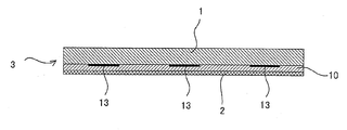
도 2는 본 발명에 사용되는 광촉매 함유층측 기판의 일례를 나타내는 개략 단면도이다.2 is a schematic cross-sectional view showing an example of the photocatalyst-containing layer side substrate used in the present invention.
도 3은 본 발명에 사용되는 광촉매 함유층측 기판의 다른 예를 나타내는 개략 단면도이다.3 is a schematic cross-sectional view showing another example of the photocatalyst-containing layer side substrate used in the present invention.
도 4는 본 발명에 사용되는 광촉매 함유층측 기판의 다른 예를 나타내는 개략 단면도이다.4 is a schematic cross-sectional view showing another example of the photocatalyst-containing layer side substrate used in the present invention.
도 5는 본 발명에 사용되는 광촉매 함유층측 기판의 다른 예를 나타내는 개략 단면도이다.5 is a schematic cross-sectional view showing another example of the photocatalyst-containing layer side substrate used in the present invention.
<도면의 주요 부분에 대한 부호의 설명><Explanation of symbols for main parts of the drawings>
1: 기재, 2: 광촉매 함유층, 3: 광촉매 함유층측 기판, 4: 기판, 5: 특성 변화층, 6: 패턴 형성체용 기판, 9: 특성 변화 영역, 10: 프라이머층, 13: 차광부.1: substrate, 2: photocatalyst-containing layer, 3: photocatalyst-containing layer side substrate, 4: substrate, 5: property change layer, 6: substrate for pattern forming body, 9: property change region, 10: primer layer, 13: light shielding portion.
본 발명은 광촉매를 사용하여 특성을 변화시킴에 있어서, 형성된 패턴 형성체 내에는 광촉매가 존재하지 않기 때문에, 경시적으로 열화(劣化)될 가능성이 적은 패턴 형성체의 제조 방법, 및 이 제조 방법에도 사용할 수 있는 포토마스크에 관한 것이다.In the present invention, since the photocatalyst does not exist in the formed pattern forming body when the characteristic is changed using the photocatalyst, the present invention also provides a method for producing a pattern forming product which is less likely to deteriorate with time, and this manufacturing method. It relates to a photomask that can be used.
종래부터, 고정세(高精細)한 패턴을 형성하는 방법으로서, 기재 상에 도포한 포토레지스트층에 패턴 노광을 실시하고, 노광 후, 포토레지스트를 현상하고, 또한 에칭을 하거나, 포토레지스트에 기능성을 가지는 물질을 사용하여, 포토레지스트의 노광에 의해 목적으로 하는 패턴을 직접 형성하는 등의 포토리소그래피에 의한 패턴 형성체의 제조 방법이 알려져 있다.Conventionally, as a method of forming a high-definition pattern, pattern exposure is performed on the photoresist layer apply | coated on the base material, after exposure, the photoresist is developed, an etching is performed, or the photoresist is functional. A method for producing a patterned body by photolithography, such as directly forming a target pattern by exposure of a photoresist, using a substance having a has been known.
포토리소그래피에 의한 고정세 패턴의 형성은 액정 표시 장치 등에 사용되는 컬러 필터의 착색 패턴의 형성, 마이크로렌즈의 형성, 정세한 전기 회로 기판의 제조, 패턴의 노광에 사용하는 크롬 마스크의 제조 등에 사용되고 있지만, 이들 방법에 따라서는, 포토레지스트를 사용하는 동시에, 노광 후에 액체 현상액에 의해 현상하거나, 에칭할 필요가 있으므로, 폐액(廢液)을 처리할 필요가 생기는 등의 문제점이 있고, 또 포토레지스트로서 기능성의 물질을 사용한 경우에는, 현상 시에 사용되는 알칼리액 등에 의해 열화되는 등의 문제점도 있었다.The formation of the high-definition pattern by photolithography is used for the formation of the color pattern of the color filter used in the liquid crystal display device, the formation of the microlens, the manufacture of the fine electric circuit board, the manufacture of the chrome mask used for the exposure of the pattern. In accordance with these methods, the photoresist is used, and since it is necessary to develop or etch with a liquid developer after exposure, there is a problem that a waste liquid needs to be treated. In the case of using a functional substance, there is also a problem such as deterioration due to an alkaline liquid used during development.
컬러 필터 등의 고정세한 패턴을 인쇄 등에 의해 형성하는 것도 실행되고 있지만, 인쇄로 형성되는 패턴에는, 위치 정밀도 등의 문제가 있어, 고정밀도의 패턴 형성은 곤란했다.Although forming high-definition patterns, such as a color filter by printing etc., is performed, the pattern formed by printing had problems, such as a positional precision, and high precision pattern formation was difficult.
한편, 이와 같은 문제점을 해결하기 위해, 광촉매 작용에 의해 습성(濕性)이 변화되는 물질을 사용하여 패턴을 형성하는 패턴 형성체의 제조 방법 등이 본 발명자들에서 검토되어 왔다. 그러나, 지금까지의 광촉매 작용에 의한 패턴 형성체의 제조 방법은 제조되는 패턴 형성체 자체에 광촉매가 포함되는 구성이 되기 때문에, 패턴 형성체의 종류에 따라서는, 이 광촉매에 의해 열화가 일어날 가능성이 있다고 하는 문제점을 가지는 경우도 있었다.On the other hand, in order to solve such a problem, the present inventors have examined the manufacturing method of the pattern forming body which forms a pattern using the substance whose wettability changes by a photocatalytic action. However, the conventional method for producing a patterned body by the photocatalytic action has a configuration in which the photocatalyst is included in the patterned body to be manufactured. Therefore, depending on the type of the patterned body, there is a possibility that deterioration occurs by the photocatalyst. In some cases, there was a problem.
본 발명은 상기 문제점을 감안하여 이루어진 것이며, 패턴 형성체의 제조에 있어서, 고정밀도로 패턴을 형성하는 것이 가능하여, 노광 후의 후처리가 불필요하고, 또한 제조된 패턴 형성체 내에 광촉매가 함유되어 있지 않기 때문에, 패턴 형성체 자체의 열화의 걱정도 없는 패턴 형성체의 제조 방법을 제공하는 것을 주목적으로 하는 것이다.This invention is made | formed in view of the said problem, In the manufacture of a pattern formation body, it is possible to form a pattern with high precision, the post-processing after exposure is unnecessary, and the photocatalyst is not contained in the manufactured pattern formation body. Therefore, it aims at providing the manufacturing method of a pattern forming body which does not worry about deterioration of the pattern forming body itself.
상기 목적을 달성하기 위해, 본 발명은 제1항에서, 광촉매 작용에 의해 표면의 특성이 변화되는 특성 변화층을 가지는 패턴 형성체용 기판을 조제(調製)하는 패턴 형성체용 기판 조제 공정과, 광촉매를 함유하는 광촉매 함유층이 기재 상에 형성되어 이루어지는 광촉매 함유층측 기판의 광촉매 함유층과 상기 특성 변화층을 200㎛ 이하가 되도록 간극을 두고 배치한 후, 소정의 방향으로부터 에너지를 조사함으로써, 상기 특성 변화층 표면에 특성이 변화된 패턴을 형성하는 패턴 형성 공정을 가지는 것을 특징으로 하는 패턴 형성체의 제조 방법을 제공한다.In order to achieve the above object, the present invention provides a pattern forming substrate preparation step for preparing a pattern forming substrate having a property changing layer whose surface properties are changed by photocatalytic action, and a photocatalyst. The photocatalyst-containing layer containing the photocatalyst-containing layer formed on the substrate is disposed with a gap such that the photocatalyst-containing layer and the property-variable layer are 200 µm or less, and then irradiated with energy from a predetermined direction to thereby surface the property-variable layer. It has a pattern forming process which forms the pattern which the characteristic changed to, The manufacturing method of the pattern formed body characterized by the above-mentioned.
본 발명에 의하면, 특히 에너지 조사 후의 후처리도 필요없어, 여러 가지 특 성을 가지는 패턴을 고정세(高精細)하게 형성할 수 있다. 또, 에너지 조사 후, 패턴 형성체로부터 광촉매 함유층측 기판을 분리하므로, 패턴 형성체 자체에는 광촉매 함유층이 포함되지 않고, 따라서 패턴 형성체의 광촉매 작용에 의한 경시적(經時的)인 열화에 대한 걱정이 없다. 또한, 광촉매 함유층과 특성 변화층과의 간격이 전술한 범위 내이므로, 효율 양호하게 또한 정밀도가 양호한 특성이 변화된 패턴을 가지는 패턴 형성체를 얻을 수 있다.According to the present invention, the post-treatment after energy irradiation is not particularly necessary, so that a pattern having various characteristics can be formed with high definition. In addition, since the photocatalyst-containing layer-side substrate is separated from the pattern former after energy irradiation, the photocatalyst-containing layer is not included in the pattern former itself, and thus, the photocatalytic action of the pattern former against time-dependent deterioration due to the photocatalytic action There is no worry. Moreover, since the space | interval of a photocatalyst containing layer and a characteristic change layer exists in the above-mentioned range, the pattern formation body which has the pattern by which the characteristic was changed efficiently and with high precision can be obtained.
상기 제1항에 기재된 발명에서는, 제2항에 기재한 것과 같이, 상기 광촉매 함유층과 상기 특성 변화층을 0.2㎛∼1.0㎛의 범위 내가 되도록 간격을 두고 배치한 것이 바람직하다. 광촉매 함유층과 특성 변화층과의 간격이 0.2㎛∼10㎛의 범위 내이므로, 단시간의 에너지 조사에 의해 특성이 변화된 패턴을 가지는 패턴 형성체를 얻을 수 있다.In the invention according to
상기 제1항 또는 제2항에 기재된 발명에서는, 제3항에 기재한 것과 같이, 상기 광촉매 함유층측 기판이 기재와, 상기 기재 상에 패턴형으로 형성된 광촉매 함유층으로 이루어지는 것이 바람직하다. 이와 같이, 광촉매 함유층를 패턴형으로 형성함으로써, 포토마스크를 사용하지 않고 특성 변화층 상에 특성이 상이한 패턴을 형성하는 것이 가능하게 되기 때문이다. 또, 광촉매 함유층에 대응하는 면만 특성이 변화되는 것이므로, 조사하는 에너지는 특히 평행한 에너지에 한정되지 않고, 또, 에너지의 조사 방향도 특히 한정되지 않기 때문에, 에너지원의 종류 및 배치의 자유도가 대폭 증가한다고 하는 이점을 갖기 때문이다.In the invention according to
상기 제1항 또는 제2항에 기재된 발명에서는, 제4항에 기재한 것과 같이, 상 기 광촉매 함유층측 기판이 기재와, 상기 기재 상에 형성된 광촉매 함유층과, 패턴형으로 형성된 차광부로 이루어지고, 상기 패턴 형성 공정에서의 에너지의 조사가 광촉매 함유층측 기판으로부터 실행되는 것이 바람직하다.In the invention according to
이와 같이 광촉매 함유층측 기판에 차광부를 가짐으로써, 에너지 조사에 있어서 포토마스크 등을 사용할 필요가 없기 때문에, 포토마스크와 위치 맞춤 등이 불필요하게 되어, 공정을 간략화하는 것이 가능하게 되기 때문이다.This is because by having the light shielding portion in the photocatalyst-containing layer side substrate, there is no need to use a photomask or the like for energy irradiation, so that the photomask and the alignment are not necessary, and the process can be simplified.
상기 제4항에 기재된 발명에서는, 제5항에 기재한 것과 같이, 상기 광촉매 함유층측 기판에서, 상기 차광부가 상기 기재 상에 패턴형으로 형성되고, 또한 그 위에 상기 광촉매 함유층이 형성되어 있는 것이라도 되고, 또 제6항에 기재한 것과 같이, 상기 광촉매 함유층측 기판에서, 상기 기재 상에 광촉매 함유층이 형성되고, 상기 광촉매 함유층 상에 상기 차광부가 패턴형으로 형성되어 있는 것이라도 된다.In the invention according to
차광부는 특성 변화층에 가까운 위치에 배치되는 것이 얻어지는 특성패턴의 정밀도 상 바람직한 것이라고 할 수 있다. 따라서, 전술한 위치에 차광부를 배치하는 것이 바람직한 것이다. 또, 광촉매 함유층 상에 차광부를 형성한 경우는, 상기 패턴 형성 공정에서의 광촉매 함유층과 특성 변화층과의 배치에 있어서의 스페이서로서 사용할 수 있다고 하는 이점을 가지는 것이다.It can be said that the light shielding portion is preferably disposed at a position close to the characteristic change layer in terms of the accuracy of the characteristic pattern obtained. Therefore, it is desirable to arrange the light shielding portion at the position described above. Moreover, when a light shielding part is formed on a photocatalyst containing layer, it has the advantage that it can be used as a spacer in arrangement | positioning of a photocatalyst containing layer and a characteristic change layer in the said pattern formation process.
상기 제2항에 기재된 발명에서는, 제7항에 기재한 것과 같이, 상기 광촉매 함유층측 기판에서, 상기 광촉매 함유층 상에 두께가 0.2㎛∼10㎛의 범위 내인 스페이서가 패턴형으로 형성되어 있고, 상기 스페이서와 상기 특성 변화층을 접촉시켜 노광시키는 것이 바람직하다.
In the invention according to
이와 같이, 광촉매 함유층 상에 패턴형으로 스페이서를 설치하고, 이것을 특성 변화층과 접촉시키도록 하여 노광함으로써, 광촉매 함유층과 특성 변화층과의 거리를 0-2㎛∼10㎛의 범위 내에 용이하게 유지하는 것이 가능하게 된다. 또, 이 스페이서가 형성된 부분은 광촉매 함유층이 스페이서에 의해 덮히기 때문에, 이 부분은 에너지 조사되어도 특성 변화층 상의 특성에 변화가 생기지 않는다. 따라서, 스페이서가 형성된 패턴과 동일 패턴으로 특성 변화층 상에 특성이 상이한 패턴을 형성하는 것이 가능하게 된다.Thus, by providing a spacer in a pattern shape on the photocatalyst-containing layer and exposing it to be in contact with the property change layer, the distance between the photocatalyst-containing layer and the property change layer is easily maintained within a range of 0-2 탆 to 10 탆. It becomes possible. In addition, since the photocatalyst-containing layer is covered by the spacer in the portion where the spacer is formed, the portion does not change in the characteristics on the characteristic change layer even when energy is irradiated. Therefore, it becomes possible to form the pattern from which a characteristic differs on a characteristic change layer in the same pattern as the pattern in which the spacer was formed.
상기 제7항에 기재된 발명에서는, 제8항에 기재한 것과 같이, 상기 스페이서가 차광성의 재료로 형성된 차광부인 것이 바람직하다. 스페이서가 차광부이므로, 차광부를 특성 변화층에 밀착시킨 상태로 에너지 조사를 실시함으로써, 보다 고정세한 패턴을 형성하는 것이 가능하게 되기 때문이다.In the invention according to
본 발명은 또, 제9항에 기재한 것과 같이, 투명한 기재 상에 차광부가 패턴형으로 형성된 포토마스크 상에 프라이머층을 통해 광촉매 함유층이 형성된 광촉매 함유층측 기판과, 적어도 상기 광촉매 함유층 중의 광촉매 작용에 의해 특성이 변화되는 특성 변화층을 가지는 패턴 형성체용 기판을 상기 광촉매 함유층 및 상기 패턴 형성체용 기판이 접촉하도록 배치하고, 또는 상기 광촉매 함유층의 광촉매 작용이 상기 특성 변화층에 미치는 거리를 떨어지게 하여 상기 광촉매 함유층측 기판을 배치한 후, 에너지를 조사함으로써, 조사된 부분의 특성 변화층의 특성을 변화시키고, 이어서, 광촉매 함유층측 기판을 분리함으로써 특성이 변화된 패턴을 형성하는 것을 특징으로 하는 패턴 형성체의 제조 방법을 제공한다. The present invention also provides a photocatalyst-containing layer-side substrate in which a photocatalyst-containing layer is formed through a primer layer on a photomask on which a light shield is formed in a pattern on a transparent substrate, and at least the photocatalytic action in the photocatalyst-containing layer. The photocatalyst-containing layer and the pattern-form substrate are in contact with each other, or the photocatalyst-containing layer has a characteristic-changing layer whose characteristics are changed by contacting the substrate. After arranging the containing layer side substrate, energy is irradiated to change the properties of the characteristic change layer of the irradiated portion, and then the photocatalyst containing layer side substrate is separated to form a pattern having changed characteristics. It provides a manufacturing method.
본 발명에 의하면, 특히 에너지 조사 후의 후처리도 필요 없어, 고감도로 고정세한 패턴을 제조할 수 있다. 또, 에너지 조사 후, 패턴으로부터 광촉매 함유층측 기판을 분리하므로, 특성 변화층측 기판 자체에는 광촉매 함유층이 포함되지 않고, 따라서 광촉매 작용에 의한 경시적인 열화에 대한 걱정이 없다. 또한, 프라이머층의 효과에 의해, 상기 차광부를 패터닝할 때에 발생하여 차광부 또는 차광부 사이의 개구부에 존재하는 찌꺼기 등이, 광촉매 작용에 영향을 주지 않는다. 따라서, 광촉매의 감도를 향상시키는 것이 가능하여, 단시간의 에너지 조사에 의해 특성이 변화된 패턴을 얻을 수 있다.According to the present invention, the post-treatment after energy irradiation is not particularly necessary, and a highly precise pattern can be produced. In addition, since the photocatalyst-containing layer-side substrate is separated from the pattern after energy irradiation, the photocatalyst-containing layer is not included in the characteristic change layer-side substrate itself, and thus there is no worry about deterioration with time due to the photocatalytic action. Further, due to the effect of the primer layer, debris and the like, which occur when patterning the light shielding portion and present in the light shielding portion or the opening between the light shielding portions, do not affect the photocatalytic action. Therefore, it is possible to improve the sensitivity of the photocatalyst, and to obtain a pattern in which the characteristic is changed by energy irradiation for a short time.
상기 제9항에 기재된 발명에서는, 제10항에 기재한 것과 같이, 상기 광촉매 함유층의 광촉매 작용이 상기 특성 변화층에 미치는 거리가, 0.2㎛∼10㎛의 범위 내인 것이 바람직하다. 광촉매 함유층과 특성 변화층과의 간격이 O.2㎛∼10㎛의 범위 내이므로, 단시간의 에너지 조사에 의해 특성이 변화된 패턴을 가지는 패턴 형성체를 얻을 수 있기 때문이다.In the invention according to
상기 제1항 내지 제10항 중 어느 한 항에 기재된 발명에서는, 제11항에 기재한 것과 같이, 상기 광촉매 함유층이 광촉매로 이루어지는 층인 것이 바람직하다. 광촉매 함유층이 광촉매만으로 이루어지는 층이면, 특성 변화층의 특성을 변화시키는 효율을 향상시키는 것이 가능하여, 효율적으로 패턴 형성체를 제조할 수 있기 때문이다.In the invention according to any one of
상기 제11항에 기재된 발명에서는, 제12항에 기재한 것과 같이, 상기 광촉매 함유층이 광촉매를 진공 제막법에 의해 기재 상에 제막하여 이루어지는 층인 것이 바람직하다. 이와 같이 진공 제막법에 의해 광촉매 함유층을 형성함으로써, 표면의 요철이 적고 균일한 막 두께의 균질(均質)한 광촉매 함유층으로 하는 것이 가능하여, 특성 변화층 표면에의 특성 패턴의 형성을 균일하게 또한 고효율로 실행할 수 있기 때문이다.In the invention according to claim 11, as described in claim 12, the photocatalyst-containing layer is preferably a layer formed by forming a photocatalyst on a substrate by a vacuum film forming method. By forming the photocatalyst-containing layer by the vacuum film forming method in this way, it is possible to obtain a homogeneous photocatalyst-containing layer having a small unevenness on the surface and a uniform film thickness. This is because it can be executed with high efficiency.
상기 제1항 내지 제10항 중 어느 한 항에 기재된 발명에서는, 제13항에 기재한 것과 같이, 상기 광촉매 함유층이 광촉매와 바인더를 가지는 층이라도 된다. 이와 같이 바인더를 사용함으로써, 비교적 용이하게 광촉매 함유층을 형성하는 것이 가능하게 되어, 결과적으로 저비용으로 패턴 형성체의 제조를 실행할 수 있기 때문이다.In the invention according to any one of
상기 제1항 내지 제13항 중 어느 한 항에 기재된 발명에서는, 제14항에 기재한 것과 같이, 상기 광촉매가 산화 티탄(TiO2), 산화 아연(ZnO), 산화 주석(SnO2), 티탄산 스트론튬(SrTiO3), 산화 텅스텐(WO3), 산화 비스무트(Bi2O3
), 및 산화철(Fe2O3)에서 선택되는 1종 또는 2종 이상의 물질인 것이 바람직하고, 그 중에서도 제15항에 기재한 것과 같이, 상기 광촉매가 산화 티탄(TiO2)인 것이 바람직하다. 이것은, 이산화 티탄의 밴드갭 에너지가 높기 때문에 광촉매로서 유효하고, 또한 화학적으로도 안정되고 독성도 없으며, 입수도 용이하기 때문이다.In the invention according to any one of
상기 제1항 내지 제15항 중 어느 한 항에 기재된 발명에서는, 제16항에 기재한 것과 같이, 상기 패턴 형성체용 기판이 적어도 기판과 이 기판 상에 설치된 상기 특성 변화층으로 형성되어 있는 것이 바람직하다. 이것은, 통상 특성 변화층은 여러 가지 특성을 가지기 때문에, 강도면, 비용면 및 기능면에서 기판 상에 박막으로서 형성되는 것이 바람직하기 때문이다.In the invention according to any one of
제16항에 기재된 발명에서는, 제17항에 기재한 것과 같이, 상기 특성 변화층이 광촉매 함유층 중의 광촉매 작용에 따라, 에너지 조사되었을 때에 액체와의 접촉각이 저하되도록 습성이 변화되는 습성 변화층인 것이 바람직하다. 이 특성 변화층의 특성은 여러 가지가 있지만, 그 중에서도 중요한 것으로서 습성의 변화를 들 수 있다. 이와 같이 특성 변화층을 습성 변화층으로 함으로써, 광촉매 작용에 의해 습성이 변화된 패턴을 가지는 패턴 형성체로 하는 것이 가능하게 되며, 이 습성이 변화된 부위에 잉크 등의 기능성부용 조성물을 부착시킴으로써, 후술하는 것과 같이 여러 가지 기능성 소자, 예를 들면 컬러 필터나 마이크로렌즈 등을 형성할 수 있기 때문이다.In the invention according to claim 16, as described in claim 17, the property-changing layer is a wet-changing layer in which the wettability is changed so that the contact angle with the liquid decreases when energy is irradiated according to the photocatalytic action in the photocatalyst-containing layer. desirable. There are various characteristics of this characteristic change layer, but among these, an important change is the habit. Thus, by making a property change layer into a moisture change layer, it becomes possible to set it as the pattern formation body which has a pattern by which a change in the wet property by the photocatalytic effect is carried out. This is because various functional elements such as color filters, microlenses and the like can be formed.
상기 제17항에 기재된 발명에서는, 제18항에 기재한 것과 같이, 상기 습성 변화층 상에서의 표면 장력 40mN/m의 액체와의 접촉각이 노광되어 있지 않은 부분에서 10°이상이며, 노광된 부분에서 9°이하인 것이 바람직하다. 에너지가 조사되어 있지 않은 부분은 발액성(撥液性)이 요구되는 부분이며, 조사된 부분은 친액성(親液性)이 요구되는 부분이기 때문에, 이 정도의 습성일 필요가 있기 때문이다.In the invention described in claim 17, as described in claim 18, the contact angle with a liquid having a surface tension of 40 mN / m on the wetted change layer is 10 ° or more in the unexposed portion, in the exposed portion. It is preferable that it is 9 degrees or less. This is because the part where energy is not irradiated is a part where liquid repellency is required, and the irradiated part is a part where lyophilic property is required, and therefore it is necessary to be wet at this level.
상기 제17항 또는 제18항에 기재된 발명에서는, 제19항에 기재한 것과 같이, 상기 습성 변화층이 오르가노폴리실록산을 함유하는 층인 것이 바람직하고, 그 중에서도 제20항에 기재한 것과 같이, 상기 오르가노폴리실록산이 플루오로알킬기를 함유하는 폴리실록산인 것이 바람직하다. 이와 같은 습성 변화층은, 광촉매 함유 층이 접촉한 상태에서의 에너지 조사에 의해, 대폭적인 습성의 변화를 얻을 수 있기 때문이다.In the invention according to claim 17 or 18, as described in claim 19, the wetted change layer is preferably a layer containing an organopolysiloxane, and in particular, as described in claim 20, It is preferable that the organopolysiloxane is a polysiloxane containing a fluoroalkyl group. This wet change layer is because a significant change in wetness can be obtained by energy irradiation in a state where the photocatalyst-containing layer is in contact with each other.
상기 제19항 또는 제20항 기재의 발명에서는, 제21항에 기재한 것과 같이, 상기 오르가노폴리실록산이 YnSiX(4-n)(여기에서, Y는 알킬기, 플루오로알킬기, 비닐기, 아미노기, 페닐기 또는 에폭시기를 나타내고, X는 알콕실기 또는 할로겐을 나타냄. n은 0∼3까지의 정수(整數)임)으로 표시되는 규소 화합물의 1종 또는 2종 이상의 가수 분해 축합물(縮合物) 또는 공(共)가수 분해 축합물인 오르가노폴리실록산인 것이 바람직하다. 이와 같은 오르가노폴리실록산을 재료로 하여 습성 변화층을 형성함으로써 습성의 차이가 큰 습성 패턴이 형성된 패턴 형성체로 할 수 있기 때문이다.In the invention according to claim 19 or 20, as described in claim 21, the organopolysiloxane is Y n SiX (4-n) , wherein Y is an alkyl group, a fluoroalkyl group, a vinyl group, An amino group, a phenyl group or an epoxy group, X represents an alkoxyl group or a halogen, n is an integer of 0 to 3) or one or two or more hydrolysis-condensates of the silicon compound represented by Or organopolysiloxane which is a co-hydrolysis condensate is preferable. It is because it can be set as the pattern formation body in which the wet pattern with a large difference in wettability was formed by forming a wetness change layer using such organopolysiloxane as a material.
상기 제1항 내지 제15항 중 어느 한 항 기재의 발명에서는 제22항에 기재한 것과 같이, 상기 패턴 형성체용 기판이 자기 지지성을 가지는 필름이며, 그 적어도 한 쪽 표면이 광촉매 함유층 중의 광촉매 작용에 의해, 에너지 조사되었을 때에 액체와의 접촉각이 저하되도록 습성이 변화되는 필름형의 습성 변화층이라도 된다. 이와 같은 패턴 형성체는, 예를 들면 소정의 재질로 이루어지는 시판 필름의 한 쪽 표면에 광촉매 함유층과 접촉시킨 상태에서 에너지 조사하는 것만으로, 습성이 상이한 패턴을 얻는 것이 가능해, 염가의 패턴 형성체로 할 수 있기 때문이다.In the invention according to any one of
상기 제16항에 기재된 발명에서는, 제23항에 기재한 것과 같이, 상기 특성 변화층이 광촉매 함유층 중의 광촉매 작용에 의해 분해 제거되는 분해 제거층이라 도 된다. 이와 같이, 특성 변화층을 광촉매 함유층 중의 광촉매 작용에 의해 분해 제거되는 분해 제거층으로 함으로써, 에너지 조사된 부분은 광촉매 작용에 의해 분해되어 제거되게 된다. 이와 같이 에너지가 조사된 부분은, 특히 후처리의 필요성도 없이 완전히 분해 제거하는 것이 가능하기 때문에, 예를 들면 분해 제거층을 포토레지스트로 하고, 여기에 광촉매 함유층측 기판을 접촉시켜 노광함으로써, 종래 실행되어 온 현상 공정을 실행할 필요 없이 포토레지스트에 패턴을 형성할 수 있는 등의 여러 가지 용도가 있기 때문이다.In the invention described in claim 16, as described in claim 23, the property change layer may be a decomposition removal layer that is decomposed and removed by a photocatalytic action in the photocatalyst-containing layer. In this way, by using the property change layer as the decomposition removal layer that is decomposed and removed by the photocatalytic action in the photocatalyst-containing layer, the energy-irradiated portion is decomposed and removed by the photocatalytic action. Since the energy-irradiated portion can be completely decomposed and removed without the need for post-treatment in particular, for example, by using a decomposable removal layer as a photoresist and bringing the photocatalyst-containing layer side substrate into contact therewith, This is because there are various uses, such as being able to form a pattern in a photoresist without having to execute a developing process that has been performed.
상기 제23항 기재의 발명에서는, 제24항에 기재한 것과 같이, 상기 분해 제거층과 이 분해 제거층이 분해 제거되었을 때에 노출되는 기판과의 액체와의 접촉각이 상이한 것이 바람직하다.In the invention described in the twenty-third aspect of the present invention, as described in the twenty-fourth aspect, it is preferable that the contact angle between the decomposition removal layer and the substrate exposed when the decomposition removal layer is removed is different.
이와 같이, 분해 제거층과 이 분해 제거층이 분해 제거되었을 때에 노출되는 기판과의 액체와의 접촉각이 상이함으로써, 에너지 조사된 부분은 광촉매 작용에 의해 분해 제거층이 분해 제거되어 기재가 표면에 노출되게 된다. 한편, 에너지 조사되어 있지 않은 부분은 분해 제거층이 잔존하게 된다. 여기에서, 분해 제거층과 노출된 기재에서 액체와의 접촉각이 상이한 것인 경우, 예를 들면 분해 제거층을 발액성의 재료로 형성하고, 기재를 친액성의 재료로 형성한 경우 등에서는, 미리 기능성부를 형성하는 부분에 에너지를 조사하여 광촉매를 작용시킴으로써 그 부분의 분해 제거층을 제거할 수 있으며, 에너지를 조사한 부분은 오목부이고 또한 친액성 영역이 되며, 에너지를 조사하지 않는 부분은 볼록부이고 또한 발액성 영역이 된다. 이에 따라, 이 기능성부를 설치하는 오목부이고 또한 친액성 영역의 부 분에 기능성부용 조성물을 정확 또한 용이하게 부착시킬 수 있다. 따라서 전술한 특성 변화층이 습성 변화층인 경우보다 더욱 정확하게 기능성부를 형성할 수 있고, 또한 현상 공정 또는 세정 공정 등의 에너지 조사 후의 후처리를 실행할 필요가 없다. 이 때문에, 용이하게 공정을 간략화하는 것이 가능하여, 염가 또한 정확한 기능성부를 가지는 기능성 소자를 얻을 수 있다.In this way, the contact angles between the decomposition removal layer and the liquid exposed to the substrate exposed when the decomposition removal layer is decomposed and removed are different, so that the energy-exposed portion is decomposed and removed by the photocatalytic action to expose the substrate to the surface. Will be. On the other hand, in the part not irradiated with energy, the decomposition removal layer remains. Here, in the case where the contact angle between the decomposition removal layer and the exposed substrate is different from the liquid, for example, when the decomposition removal layer is formed of a liquid-repellent material, and the substrate is formed of a lyophilic material, etc., The photocatalyst can be removed by irradiating energy to a portion forming the functional portion to remove the decomposition-removing layer of the portion, and the irradiated portion is a concave portion and a lyophilic region, and the portion not irradiating energy is a convex portion. And also a liquid repellent region. Thereby, the composition for functional parts can be correctly and easily attached to the recessed part which provides this functional part, and to the part of a lyophilic region. Therefore, the functional part can be formed more accurately than when the above-described property change layer is a wet change layer, and there is no need to perform post-treatment after energy irradiation such as a developing step or a cleaning step. For this reason, a process can be easily simplified and a functional element which has a cheap and accurate functional part can be obtained.
상기 제23항 또는 제24항 기재의 발명에서는, 제25항에 기재한 것과 같이, 상기 분해 제거층이 자기 조직화 단분자막, 랑그뮤어 블로드제트(Langmuir-Blodgett)막, 또는 교대 흡착막 중 어느 하나인 것이 바람직하다. 이들 재료가 광촉매 함유층 중의 광촉매 작용에 의해 분해 제거되어, 여러 가지 기능을 발휘하는 것이기 때문이다.In the invention according to claim 23 or 24, as described in claim 25, the decomposition removing layer is any one of a self-organizing monomolecular film, a Langmuir-Blodgett membrane, or an alternate adsorption membrane. Is preferably. This is because these materials are decomposed and removed by the photocatalytic action in the photocatalyst-containing layer to exhibit various functions.
상기 제1항 내지 제25항 중 어느 한 항에 기재된 발명에서는, 제26항에 기재한 것과 같이, 상기 에너지 조사가 광촉매 함유층을 가열하면서 이루어지는 것이 바람직하다. 광촉매를 가열함으로써, 광촉매의 감도가 향상되어, 특성 변화층 상에서의 특성 변화를 효율적으로 실행할 수 있기 때문이다.In the invention according to any one of
본 발명에서는, 제27항에 기재한 것과 같이, 투명한 기재와, 상기 투명한 기재 상에 패턴형으로 형성된 차광부와, 상기 투명한 기재 및 차광부 상에 형성된 프라이머층과, 상기 프라이머층 상에 형성된 광촉매 함유층으로 이루어지는 것을 특징으로 하는 포토마스크를 제공한다. 이와 같은 포토마스크를 사용하면, 단지 이 포토마스크를 통해 에너지를 조사하는 것만으로, 여러 가지 특성이 변화된 패턴을 얻을 수 있어, 효율적으로 패턴 형성체를 얻을 수 있기 때문이다. In the present invention, as described in claim 27, a transparent substrate, a light shielding portion formed in a pattern shape on the transparent substrate, a primer layer formed on the transparent substrate and the light shielding portion, and a photocatalyst formed on the primer layer A photomask comprising the containing layer is provided. If such a photomask is used, only by irradiating energy through this photomask, a pattern in which various characteristics are changed can be obtained, and a pattern forming body can be efficiently obtained.
또, 본 발명에서는, 제28항에 기재한 것과 같이, 투명한 기재와, 상기 투명한 기재 상에 형성된 광촉매 함유층과, 0.2㎛∼10㎛의 두께로 상기 광촉매 함유층 상에 패턴형으로 형성된 차광부 패턴으로 이루어지는 것을 특징으로 하는 포토마스크, 및 제29항에 기재한 것과 같이 투명한 기재와, 0.2㎛∼10㎛의 두께로 상기 투명한 기재 상에 패턴형으로 형성된 차광부 패턴과, 상기 투명한 기재 및 상기 차광부 패턴형 상에 형성된 광촉매 함유층으로 이루어지는 것을 특징으로 하는 포토마스크를 제공한다. 이 경우도 마찬가지로, 이 포토마스크를 통해 전술한 것과 같은 특성 변화층을 가지는 패턴 형성체용 기판에 에너지를 조사함으로써, 여러 가지 특성이 변화된 패턴을 얻을 수 있어, 효율적으로 패턴 형성체를 얻을 수 있기 때문이다.In the present invention, as described in claim 28, a transparent substrate, a photocatalyst-containing layer formed on the transparent substrate, and a light shielding portion pattern formed in a pattern shape on the photocatalyst-containing layer in a thickness of 0.2 µm to 10 µm. A photomask comprising: and a transparent substrate as described in claim 29, a light shielding portion pattern formed in a pattern shape on the transparent substrate with a thickness of 0.2 µm to 10 µm, the transparent substrate and the shielding portion Provided is a photomask comprising a photocatalyst-containing layer formed on a pattern. In this case as well, through the photomask, energy is irradiated to the pattern forming substrate having the property changing layer as described above, whereby a pattern having various characteristics changed can be obtained, and thus the pattern forming body can be efficiently obtained. to be.
본 발명에서는 또한, 제30항에 기재한 것과 같이, 상기 제1항 내지 제26항 중 어느 한 항에 기재된 패턴 형성체의 제조 방법에 의해 제조된 패턴 형성체에, 기능성부가 배치된 것을 특징으로 하는 기능성 소자를 제공한다. 이와 같이, 본 발명의 패턴 형성체를 사용함으로써, 용이하게 기능성 소자를 얻을 수 있다.In this invention, as described in Claim 30, the functional part was arrange | positioned at the pattern formed body manufactured by the manufacturing method of the pattern formed body in any one of said Claims 1-26. A functional element is provided. In this manner, the functional element can be easily obtained by using the pattern forming body of the present invention.
상기 제30항에 기재된 기능성 소자는 상기 기능성부가 금속인 것을 들 수 있다. 이 경우는, 예를 들면 고정세한 전기 회로 기판 등에 응용하는 것이 가능하게 된다.As for the functional element of Claim 30, the said functional part is a metal. In this case, it becomes possible to apply to high-definition electrical circuit boards etc., for example.
본 발명은 또, 제32항에 기재한 것과 같이, 상기 제30항에 기재된 기능성 소자에서의 기능성부가 화소부인 것을 특징으로 하는 컬러 필터를 제공한다. 이와 같은 컬러 필터는, 고정세한 화소부가 고정밀도로 형성된 것이며, 매우 고품질인 것이다.The present invention further provides a color filter as described in claim 32, wherein the functional portion in the functional element according to the above 30 is a pixel portion. In such a color filter, a high-definition pixel portion is formed with high precision and is of very high quality.
먼저, 본 발명의 패턴 형성체의 제조 방법에 대하여 설명하고, 이어서, 이 패턴 형성체의 제조 방법에도 사용할 수 있는 포토마스크에 대하여 설명한다.First, the manufacturing method of the pattern formed body of this invention is demonstrated, Next, the photomask which can also be used for the manufacturing method of this pattern formed body is demonstrated.
A. 패턴 형성체의 제조 방법A. Manufacturing Method of Pattern Formant
본 발명의 패턴 형성체의 제조 방법은 광촉매 작용에 의해 표면의 특성이 변화되는 특성 변화층을 가지는 패턴 형성체용 기판을 조제하는 패턴 형성체용 기판 조제 공정과,The manufacturing method of the pattern formed body of this invention is a pattern forming substrate preparation process which prepares the board | substrate for pattern formation which has a characteristic change layer which changes the characteristic of the surface by a photocatalytic action,
광촉매를 함유하는 광촉매 함유층이 기재 상에 형성되어 이루어지는 광촉매 함유층측 기판의 광촉매 함유층과 상기 특성 변화층을 200㎛ 이하가 되도록 간극을 두고 배치한 후, 소정의 방향으로부터 에너지를 조사함으로써, 상기 특성 변화층 표면에 특성이 변화된 패턴을 형성하는 패턴 형성 공정After the photocatalyst-containing layer containing the photocatalyst-containing layer is formed on the substrate, the photocatalyst-containing layer of the substrate on the side of the photocatalyst-containing layer and the characteristic change layer are disposed with a gap of 200 µm or less, and then irradiated with energy from a predetermined direction, thereby changing the characteristics. Pattern formation process for forming patterns with altered properties on the layer surface
을 가지는 것을 특징으로 하는 것이다.It is characterized by having a.
이와 같이, 본 발명의 패턴 형성체의 제조 방법에서는, 광촉매 함유층 및 특성 변화층을 소정의 간극을 갖도록 배치한 후, 소정의 방향에서 에너지 조사함으로써, 광촉매 함유층 중의 광촉매 작용에 의해, 광촉매 함유층에 면하고 또한 노광한 부분의 특성 변화층의 특성이 변화되어, 이 특성 변화층 상의 특성이 변화된 부분의 패턴이 형성된다. 따라서, 패턴 형성에서 노광 후의 현상 ·세정 등의 후처리가 불필요하게 되므로, 종래보다 적은 공정이며, 또한 염가에 특성이 상이한 패턴을 형성할 수 있다. 그리고, 이 특성 변화층의 재료를 선택함으로써, 여러 가지 용도에 사용할 수 있는 패턴 형성체로 할 수 있다. Thus, in the manufacturing method of the pattern formation body of this invention, after arrange | positioning a photocatalyst containing layer and a characteristic change layer so that it may have a predetermined | prescribed clearance gap, and irradiating energy in a predetermined direction, the photocatalyst containing layer is surface-treated by the photocatalytic action in a photocatalyst containing layer. And the characteristic of the characteristic change layer of the exposed part changes, and the pattern of the part from which the characteristic on this characteristic change layer was changed is formed. Therefore, since post-processing, such as image development and washing | cleaning after exposure in a pattern formation, becomes unnecessary, it is possible to form a pattern which differs in the conventional process at low cost, and differs in characteristic at low cost. And by selecting the material of this characteristic change layer, it can be set as the pattern formation body which can be used for various uses.
또한, 본 발명에서는, 특성 변화층 상의 특성을 광촉매 함유층 중의 광촉매 작용에 의해 변화시킨 후, 광촉매 함유층측 기판을 분리하여 패턴 형성체측 기판을 패턴 형성체로 한 것이므로, 얻어지는 패턴 형성체에는 반드시 광촉매가 함유되어 있을 필요가 없다. 따라서, 얻어지는 패턴 형성체가 광촉매 작용에 의해 경시적으로 열화된다고 하는 문제점을 방지할 수 있다.In addition, in this invention, since the characteristic on a characteristic change layer is changed by the photocatalytic effect in a photocatalyst containing layer, the photocatalyst-containing layer side board | substrate was isolate | separated, and the pattern formation side board | substrate was made into the pattern formation body, Therefore, the photocatalyst obtained necessarily contains a photocatalyst. There is no need to be. Therefore, the problem that the pattern formation body obtained deteriorates with time by the photocatalytic effect can be prevented.
이와 같은 본 발명의 패턴 형성체의 제조 방법에 대하여, 도면을 사용하여 구체적으로 설명한다. 도 1은, 본 발명의 패턴 형성체 제조 방법의 일례를 나타내는 것이다.The manufacturing method of such a pattern forming body of this invention is concretely demonstrated using drawing. 1 shows an example of the method for producing a pattern formed body of the present invention.
이 예에서는, 먼저, 기재(1) 상에 광촉매 함유층(2)이 형성되어 이루어지는 광촉매 함유층측 기판(3)과, 기판(4) 상에 특성 변화층(5)이 형성되어 이루어지는 패턴 형성체용 기판(6)을 조정한다[도 1 (a)참조, 패턴 형성체용 기판 조제 공정].In this example, first, the photocatalyst-containing layer-
다음에, 도 1 (b)에 도시한 것과 같이, 상기 광촉매 함유층측 기판(3)과 패턴 형성체용 기판(6)을 각각의 광촉매 함유층(2) 및 특성 변화층(5)이 소정의 간격을 갖도록 배치한 후, 필요하게 되는 패턴이 그려진 포토마스크(7)를 사용하고, 이것을 통해 자외광(8)을 광촉매 함유층측 기판(3)측에서 조사한다. 이에 따라, 도 1 (c)에 도시한 것과 같이, 특성 변화층(5) 표면에 특성이 변화된 영역(9)으로 이루어지는 패턴이 형성된다(패턴 형성 공정).Next, as shown in Fig. 1 (b), the photocatalyst-containing
또, 상기 자외선의 조사는, 상기 예에서는 포토마스크(7)을 통한 것이지만, 후술하는 것과 같이 광촉매 함유층이 패턴형으로 형성된 것이나, 광촉매 함유층측 기판 내에 차광부가 형성된 것을 사용해도 되고, 이 경우는, 포토마스크(7) 등을 사용하지 않고, 전체면에 노광하게 된다.In addition, although the said ultraviolet irradiation irradiates through the
그리고, 상기 패턴 형성체용 기판(6) 상에서 광촉매 함유층측 기판을 떼어내는 공정이 실행되어(도 1 (d)), 표면에 특성이 변화된 패턴(9)을 가지는 패턴 형성체(6)를 얻을 수 있다.Then, a step of removing the photocatalyst-containing layer-side substrate on the
이와 같은 본 발명의 패턴 형성체의 제조 방법에 대하여, 각 요소마다 상세하게 설명한다.Such a method for producing a patterned body of the present invention will be described in detail for each element.
l.광촉매 함유층측 기판의 조정l. Adjustment of photocatalyst-containing layer side substrate
본 발명에서는 먼저 후술하는 패턴 형성 공정에서 사용하는 광촉매 함유층측 기판을 조제한다. 이 광촉매 함유층측 기판은 기재와, 이 기재 상에 형성된 광촉매를 함유하는 광촉매 함유층을 가지는 것이다.In this invention, the photocatalyst containing layer side board | substrate used at the pattern formation process mentioned later is prepared first. The photocatalyst-containing layer-side substrate has a substrate and a photocatalyst-containing layer containing a photocatalyst formed on the substrate.
이와 같은 광촉매 함유층측 기판은 적어도 광촉매 함유층과 기재를 가지는 것이며, 통상은 기재 상에 소정의 방법으로 형성된 박막형의 광촉매 함유층이 형성되어 이루어지는 것이다. 또, 이 광촉매 함유층측 기판에는 패턴형으로 형성된 차광부가 형성된 것도 사용할 수 있다.Such a photocatalyst-containing layer-side substrate has at least a photocatalyst-containing layer and a substrate, and a thin film-type photocatalyst-containing layer formed by a predetermined method is usually formed on the substrate. Moreover, what provided with the light shielding part formed in the pattern form can also be used for this photocatalyst containing layer side board | substrate.
(광촉매 함유층)(Photocatalyst-containing layer)
본 발명에 사용되는 광촉매 함유층은 광촉매 함유층 중의 광촉매가, 대상으로 하는 특성 변화층의 특성을 변화시키는 구성이면, 특히 한정되지 않고, 광촉매와 바인더로 구성되어 있는 것이라도 되고, 광촉매 단체로 제막된 것이라도 된다. 또, 그 표면의 습성은 특히 친액성이라도 발액성이라도 된다.The photocatalyst-containing layer used in the present invention is not particularly limited as long as the photocatalyst in the photocatalyst-containing layer changes the properties of the characteristic change layer, and may be composed of a photocatalyst and a binder, and formed into a single photocatalyst. You may also Moreover, the wettability of the surface may be especially lyophilic or liquid repellency.
본 발명에서 사용되는 광촉매 함유층은, 예를 들면 상기 도 1 (a) 등에 도시 한 것과 같이, 기재(1) 상에 전체면에 형성된 것이라도 되지만, 예를 들면 도 2에 도시한 것과 같이, 기재(1) 상에 광촉매 함유층(2)이 패턴 상에 형성된 것이라도 된다.The photocatalyst-containing layer used in the present invention may be formed on the entire surface of the
이와 같이 광촉매 함유층을 패턴형으로 형성함으로써, 후술하는 패턴 형성 공정에서 설명하도록, 광촉매 함유층을 특성 변화층과 소정의 간격을 두고 배치시켜 에너지를 조사할 때에, 포토마스크 등을 사용하는 패턴 조사를 할 필요가 없이, 전체면에 조사함으로써, 특성 변화층 상에 특성이 변화된 패턴을 형성할 수 있다.By forming the photocatalyst-containing layer in a patterned manner as described above, the photocatalyst-containing layer is arranged at a predetermined interval from the characteristic change layer so as to be described in a pattern forming process to be described later. There is no need to irradiate the entire surface to form a pattern on which the property is changed on the property change layer.
이 광촉매 처리층의 패터닝 방법은 특히 한정되지는 않지만, 예를 들면 포토리소그래피법 등에 의해 실행하는 것이 가능하다.Although the patterning method of this photocatalyst treatment layer is not specifically limited, For example, it can carry out by the photolithographic method etc ..
또, 실제로 광촉매 함유층에 면하는 특성 변화층 상의 부분만의 특성이 변화되는 것이므로, 에너지의 조사 방향은 상기 광촉매 함유층과 특성 변화층이 면하는 부분에 에너지가 조사되는 것이면, 어떠한 방향으로부터 조사되어도 되고, 또한, 조사되는 에너지도 특히 평행광 등의 평행한 것에 한정되지 않는다고 하는 이점을 가지게 된다.In addition, since the characteristic of only the part on the characteristic change layer which actually faces a photocatalyst containing layer changes, the direction of energy irradiation may be irradiated from any direction as long as energy is irradiated to the part which the said photocatalyst containing layer and a characteristic change layer face. In addition, the energy to be irradiated also has the advantage that it is not particularly limited to parallel ones such as parallel light.
이와 같이 광촉매 함유층에서의, 후술하는 2산화 티탄으로 대표되는 광촉매의 작용 기구는 반드시 명확한 것은 아니지만, 광의 조사에 의해 생성한 캐리어가 근방의 화합물과의 직접 반응, 또는 산소, 물의 존재 하에 생긴 활성 산소종에 의해 유기물의 화학 구조에 변화를 미치는 것으로 생각되고 있다. 본 발명에서는 이 캐리어가 광촉매 함유층 근방에 배치되는 특성 변화층 중의 화합물에 작용을 미치는 것으로 생각된다. Thus, although the mechanism of action of the photocatalyst represented by the titanium dioxide mentioned later in a photocatalyst containing layer is not necessarily clear, the active oxygen which the carrier produced | generated by irradiation of light reacted directly with the compound of the vicinity, or in presence of oxygen and water was produced. The species is thought to change the chemical structure of the organic matter. In this invention, it is thought that this carrier acts on the compound in the characteristic change layer arrange | positioned near a photocatalyst containing layer.
본 발명에서 사용하는 광촉매로서는 광반도체로서 알려지는, 예를 들면 2산화 티탄(TiO2), 산화 아연(ZnO), 산화 주석(SnO2), 티탄산 스트론튬(SrTiO3), 산화 텅스텐(WO3), 산화 비스무트(Bi2O3), 및 산화철(Fe2O3 )을 들 수 있고, 이들로부터 선택해서 1종 또는 2종 이상을 혼합하여 사용할 수 있다.As the photocatalyst used in the present invention, known as an optical semiconductor, for example, titanium dioxide (TiO 2 ), zinc oxide (ZnO), tin oxide (SnO 2 ), strontium titanate (SrTiO 3 ), tungsten oxide (WO 3 ) , Bismuth oxide (Bi 2 O 3 ), and iron oxide (Fe 2 O 3 ) may be mentioned, and one or two or more thereof may be selected and used.
본 발명에서는, 특히 2산화 티탄이 밴드갭 에너지가 높고, 화학적으로 안정되어 독성도 없고, 입수도 용이하기 때문에 적합하게 사용된다. 이산화 티탄에는, 아나타제형과 루틸형이 있고, 본 발명에서는 모두 사용할 수 있지만, 아나타제형의 2산화 티탄이 바람직하다. 아나타제형 2산화 티탄은 여기 파장이 380nm 이하에 있다.In the present invention, titanium dioxide is particularly suitably used because of its high bandgap energy, chemical stability, no toxicity, and easy availability. Titanium dioxide has an anatase type and a rutile type, and both can be used in the present invention, but anatase type titanium dioxide is preferable. The anatase titanium dioxide has an excitation wavelength of 380 nm or less.
이와 같은 아나타제형 2산화 티탄으로서는, 예를 들면, 염산 해교형(解膠型)의 아나타제형 티타니아졸(이시하라 산교(石原産業)(주)제 STS-02(평균 입경 7nm), 이시하라 산교(주)제 ST-K01), 질산 해교형의 아나타제형 티타니아졸(닛산 가가쿠(日産化學)(주)제 TA-15(평균 입경 12nm)) 등을 들 수 있다.As such anatase type titanium dioxide, the anatase type titania sol of hydrochloric acid bridge type (Ishihara Sangyo Co., Ltd. product STS-02 (average particle diameter 7nm), Ishihara Sangyo Co., Ltd.) ST-K01), the anatase type titania sol of a nitric acid bridge type (TA-15 (average particle diameter 12nm) by Nissan Chemical Co., Ltd.), etc. are mentioned.
광촉매의 입경은 작을수록 광촉매 반응이 효과적으로 일어나므로 바람직해, 평균 입경이 50nm 이하가 바람직하고, 20nm 이하의 광촉매를 사용하는 것이 특히 바람직하다.The smaller the particle size of the photocatalyst is, the more effectively the photocatalytic reaction takes place. The average particle diameter is preferably 50 nm or less, and particularly preferably 20 nm or less.
본 발명에서의 광촉매 함유층은 전술한 것과 같이 광촉매 단독으로 형성된 것이라도 되고, 또 바인더와 혼합하여 형성된 것이라도 된다.The photocatalyst-containing layer in the present invention may be formed of a photocatalyst alone as described above, or may be formed by mixing with a binder.
광촉매만으로 이루어지는 광촉매 함유층의 경우는, 특성 변화층 상의 특성 변화에 대한 효율이 향상되고, 처리 시간의 단축화 등의 비용면에서 유리하다. 한편, 광촉매와 바인더로 이루어지는 광촉매 함유층의 경우는 광촉매 함유층의 형성이 용이하다고 하는 이점을 가진다.In the case of the photocatalyst containing layer which consists only of a photocatalyst, the efficiency with respect to the characteristic change on a characteristic change layer improves, and it is advantageous in terms of cost, such as shortening processing time. On the other hand, in the case of the photocatalyst containing layer which consists of a photocatalyst and a binder, it has the advantage that formation of a photocatalyst containing layer is easy.
광촉매만으로 이루어지는 광촉매 함유층의 형성 방법으로서는, 예를 들면, 스퍼터링법, CVD법, 진공 증착법 등의 진공 제막법을 사용하는 방법을 들 수 있다. 진공 제막법에 의해 광촉매 함유층을 형성함으로써, 균일한 막으로 또한 광촉매만을 함유하는 광촉매 함유층으로 하는 것이 가능하며, 이에 따라 특성 변화층 상의 특성을 균일하게 변화시키는 것이 가능하고, 또한 광촉매만으로 이루어지기 때문에, 바인더를 사용하는 경우와 비교하여 효율적으로 특성 변화층 상의 특성을 변화시키는 것이 가능하게 된다.As a formation method of the photocatalyst containing layer which consists only of a photocatalyst, the method of using the vacuum film forming methods, such as a sputtering method, a CVD method, and a vacuum vapor deposition method, is mentioned, for example. By forming the photocatalyst-containing layer by the vacuum film forming method, it is possible to form a photocatalyst-containing layer containing only the photocatalyst with a uniform film, and thus it is possible to uniformly change the characteristics on the characteristic change layer, and only the photocatalyst. As compared with the case of using a binder, it becomes possible to change the characteristic on a characteristic change layer more efficiently.
또, 광촉매만으로 이루어지는 광촉매 함유층의 형성 방법으로서는, 예를 들면 광촉매가 2산화 티탄인 경우는, 기재 상에 무정형(無定形) 티타니아를 형성하고, 이어서 소성(燒成)에 의해 결정성 티타니아에 상변화시키는 방법 등을 들 수 있다. 여기서 사용되는 무정형 티타니아로서는, 예를 들면 4염화 티탄, 황산 티탄 등 티탄의 무기염 가수 분해, 탈수 축합(縮合), 테트라에톡시티탄, 테트라이소프로폭시티탄, 테트라-n-프로폭시티탄, 테트라부톡시티탄, 테트라메톡시티탄 등의 유기 티탄 화합물을 산(酸) 존재 하에 가수 분해, 탈수 축합에 의해 얻을 수 있다. 이어서, 400℃∼500℃에서의 소성에 의해 아나타제형 티타니아로 변성(變性)되고, 600℃∼700℃의 소성에 의해 루틸형 티타니아로 변성할 수 있다.Moreover, as a formation method of the photocatalyst containing layer which consists only of a photocatalyst, when a photocatalyst is titanium dioxide, for example, amorphous titania is formed on a base material, and then it forms on crystalline titania by baking. The method of changing, etc. are mentioned. Examples of the amorphous titania used herein include inorganic salt hydrolysis, dehydration condensation of titanium such as titanium tetrachloride and titanium sulfate, tetraethoxytitanium, tetraisopropoxytitanium, tetra-n-propoxycitane and tetra Organic titanium compounds such as butoxytitanium and tetramethoxytitanium can be obtained by hydrolysis and dehydration condensation in the presence of an acid. Subsequently, it can be modified to anatase-type titania by firing at 400 ° C to 500 ° C, and can be modified to rutile titania by firing at 600 ° C to 700 ° C.
또, 바인더를 사용하는 경우는, 바인더의 주골격이 상기 광촉매의 광여기에 의해 분해되지 않는 높은 결합 에너지를 가지는 것이 바람직하고, 예를 들면 오르가노폴리실록산 등을 들 수 있다.Moreover, when using a binder, it is preferable that the main skeleton of a binder has high binding energy which is not decomposed by the photoexcitation of the said photocatalyst, For example, an organopolysiloxane etc. are mentioned.
이와 같이 오르가노폴리실록산을 바인더로서 사용한 경우는, 상기 광촉매 함유층은 광촉매와 바인더인 오르가노폴리실록산을 필요에 따라 다른 첨가제와 함께 용제 중에 분산하여 도포액을 조제하고, 이 도포액을 기재 상에 도포함으로써 형성할 수 있다. 사용하는 용제로서는 에탄올, 이소프로파놀 등 알콜계의 유기 용제(溶劑)가 바람직하다. 도포는 스핀 코트, 스프레이 코트, 딥 코트, 롤 코트, 비드 코트 등 공지된 도포방법에 의해 실행할 수 있다. 바인더로서 자외선 경화형의 성분을 함유하고 있는 경우, 자외선을 조사하여 경화 처리를 실행함으로써 광촉매 함유층을 형성할 수 있다.Thus, when organopolysiloxane is used as a binder, the said photocatalyst containing layer disperse | distributes the organopolysiloxane which is a photocatalyst and a binder with another additive as needed, prepares a coating liquid, and apply | coats this coating liquid on a base material by Can be formed. As a solvent to be used, an organic solvent of alcohol type, such as ethanol and isopropanol, is preferable. Coating can be performed by a well-known coating method, such as a spin coat, a spray coat, a dip coat, a roll coat, a bead coat. When the ultraviolet curable component is contained as the binder, the photocatalyst-containing layer can be formed by irradiating ultraviolet rays and performing a curing treatment.
또, 바인더로서 무정형 실리카 전구체(前驅體)를 사용할 수 있다. 이 무정형 실리카 전구체는, 일반식 SiX4로 표시되고, X는 할로겐, 메톡시기, 에톡시기, 또는 아세틸기 등인 규소 화합물, 이들의 가수 분해물인 실라놀, 또는 평균 분자량 3000 이하의 폴리실록산이 바람직하다.Moreover, an amorphous silica precursor can be used as a binder. This amorphous silica precursor is represented by general formula SiX 4 , and a silicon compound in which X is a halogen, a methoxy group, an ethoxy group or an acetyl group, silanol which is a hydrolyzate thereof, or polysiloxane having an average molecular weight of 3000 or less is preferable.
구체적으로는, 테트라에톡시실란, 테트라이소프로폭시실란, 테트라n-프로폭시실란, 테트라부톡시실란, 테트라메톡시실란 등을 들 수 있다. 또, 이 경우에는, 무정형 실리카의 전구체와 광촉매의 입자를 비수성 용매 중에 균일하게 분산시키고, 기재 상에 공기 중의 수분에 의해 가수 분해시켜 실라놀을 형성시킨 후, 상온으로 탈수 축중합(縮重合)함으로써 광촉매 함유층를 형성할 수 있다. 실라놀의 탈 수 축중합을 100℃ 이상으로 실행하면, 실라놀의 중합도가 증가하여, 막표면의 강도를 향상시킬 수 있다. 또, 이들 결착제는, 단독 또는 2종 이상을 혼합하여 사용할 수 있다.Specifically, tetraethoxysilane, tetraisopropoxysilane, tetran-propoxysilane, tetrabutoxysilane, tetramethoxysilane, etc. are mentioned. In this case, the precursor of amorphous silica and the particles of the photocatalyst are uniformly dispersed in a non-aqueous solvent, hydrolyzed by moisture in the air on the substrate to form silanol, and then dehydrated and condensation polymerization at room temperature. The photocatalyst-containing layer can be formed. When dehydration and condensation polymerization of silanol is performed at 100 degreeC or more, the polymerization degree of silanol will increase and the film surface strength can be improved. Moreover, these binders can be used individually or in mixture of 2 or more types.
바인더를 사용한 경우의 광촉매 함유층 중의 광촉매의 함유량은, 5∼60중량%, 바람직하게는 20∼40중량%의 범위에서 설정할 수 있다. 또, 광촉매 함유층의 두께는, 0.05∼10㎛의 범위 내가 바람직하다.Content of the photocatalyst in the photocatalyst containing layer at the time of using a binder can be set in 5 to 60 weight%, Preferably it is 20 to 40 weight%. Moreover, the inside of the range whose thickness of a photocatalyst containing layer is 0.05-10 micrometers is preferable.
또, 광촉매 함유층에는 상기 광촉매, 바인더 외에 계면 활성제를 함유시킬 수 있다. 구체적으로는, 닛코(日光) 케미칼즈(주)제 NIKKOL BL, BC, BO, BB의 각 시리즈 등의 탄화 수소계, 듀퐁사제 ZONYL FSN, FSO, 아사히 가라스(旭硝子)(주)제 사프론 S-14l, l45, 다이닛폰(大日本) 잉키 가가쿠 고교(주)제 메가파크 F-l4l, 144, 네오스(주)제 부타젠트 F-200, F251, 다이킨 고교(주)제 유니다인 DS-401, 402, 스리엠(주)제 플로라드 FC-l70, 176 등의 불소계 또는 실리콘계의 비(非)이온 계면 활성제를 들 수 있고, 또, 양이온계 계면 활성제, 음이온계 계면 활성제, 양성(兩性) 계면 활성제를 사용할 수도 있다.The photocatalyst-containing layer may contain a surfactant in addition to the photocatalyst and the binder. Specifically, hydrocarbons such as NIKKOL BL, BC, BO, and BB series manufactured by Nikko Chemicals Co., Ltd., ZONYL FSN, FSO, manufactured by DuPont, and Saffron, manufactured by Asahi Glass Co., Ltd. S-14l, l45, Dainippon Inky Kagaku Kogyo Co., Ltd. Mega Park F-l4l, 144, Neos Co., Ltd. Butagent F-200, F251, Daikin High Co., Ltd. Fluorine-based or silicon-based nonionic surfactants such as DS-401, 402, and SML Co., Ltd., Florard FC-l70, 176; and cationic surfactants, anionic surfactants, and amphoterics. A surfactant can also be used.
또한, 광촉매 함유층에는 상기 계면 활성제 외에도, 폴리비닐 알콜, 불포화 폴리에스테르, 아크릴 수지, 폴리에틸렌, 디아릴부탈에이트, 에틸렌프로필렌디엔모노머, 에폭시 수지, 페놀 수지, 폴리우레탄, 멜라민수지, 폴리카보네이트, 폴리염화 비닐, 폴리아미드, 폴리이미드, 스티렌부타디엔 고무, 클로로프렌 고무, 폴리프로필렌, 폴리부틸렌, 폴리스티렌, 폴리아세트산 비닐, 폴리에스테르, 폴리부타디엔, 폴리벤즈이미다졸, 폴리아크릴니트릴, 에피크롤히드린, 폴리살파이드,폴리이소 프렌 등의 올리고머, 폴리머 등을 함유시킬 수 있다.In addition to the above surfactants, the photocatalyst-containing layer also contains polyvinyl alcohol, unsaturated polyester, acrylic resin, polyethylene, diarylbutalate, ethylene propylene diene monomer, epoxy resin, phenol resin, polyurethane, melamine resin, polycarbonate, polychloride Vinyl, polyamide, polyimide, styrenebutadiene rubber, chloroprene rubber, polypropylene, polybutylene, polystyrene, polyvinyl acetate, polyester, polybutadiene, polybenzimidazole, polyacrylonitrile, epicrohydrin, polysal Oligomers, polymers, etc., such as a phide and polyisoprene, can be contained.
(기재)(materials)
본 발명에서는, 도 1에 도시한 것과 같이, 광촉매 함유층측 기판3은 적어도 기재(1)와 이 기재(1)상에 형성된 광촉매 함유층(2)을 가지는 것이다.In the present invention, as shown in FIG. 1, the photocatalyst-containing layer-
이때, 사용되는 기재를 구성하는 재료는 후술하는 패턴 형성 공정에서의 에너지의 조사 방향이나, 얻어지는 패턴 형성체가 투명성을 필요로 하는가 등에 따라 적당히 선택된다.At this time, the material which comprises the base material used is suitably selected according to the irradiation direction of energy in the pattern formation process mentioned later, whether the pattern forming body obtained needs transparency, etc.
즉, 예를 들면 패턴 형성체가 불투명한 것을 기판으로서 사용하는 경우에서는, 에너지 조사 방향은 필연적으로 광촉매 함유층측 기판측으로부터 되고, 도 1 (b)에 도시한 것과 같이, 포토마스크(7)를 광촉매 함유층측 기판(3)측에 배치하여, 에너지 조사를 할 필요가 있다. 또, 후술하는 것과 같이 광촉매 함유층측 기판에 차광부를 미리 소정의 패턴으로 형성해 두고, 이 차광부를 사용하여 패턴을 형성하는 경우에도, 광촉매 함유층측 기판측으로부터 에너지를 조사할 필요가 있다. 이와 같은 경우, 기재는 투명성을 가지는 것이 필요하게 된다.That is, for example, in the case where a pattern forming body is used as a substrate, the direction of energy irradiation necessarily comes from the photocatalyst-containing layer side substrate side, and the
한편, 패턴 형성체가 투명한 경우이면, 패턴 형성체용 기판측에 포토마스크를 배치하여 에너지를 조사하는 것도 가능하다. 또, 이 패턴 형성체용 기판 내에 패턴 형성체측 차광부를 형성하는 경우는, 패턴 형성체용 기판측으로부터 에너지를 조사할 필요가 있다. 이와 같은 경우에서는, 기재의 투명성이 특히 필요하게 되지 않는다.On the other hand, if the pattern forming body is transparent, it is also possible to arrange | position a photomask on the substrate side for pattern formation, and to irradiate energy. Moreover, when forming a pattern formation side light shielding part in this pattern formation substrate, it is necessary to irradiate energy from the substrate for a pattern formation body. In such a case, transparency of the substrate is not particularly required.
또한 본 발명에 사용되는 기재는 가요성(可撓性)을 가지는 것, 예를 들면 수 지제 필름 등이라도 되고, 가요성을 갖지 않은 것, 예를 들면 유리 기판 등이라도 된다. 이것은 후술하는 패턴 형성 공정에서의 에너지 조사 방법에 의해 적당히 선택되는 것이다.In addition, the base material used for this invention may be a thing with flexibility, for example, a resin film, etc., and a thing without flexibility, for example, a glass substrate. This is suitably selected by the energy irradiation method in the pattern formation process mentioned later.
이와 같이, 본 발명에서의 광촉매 함유층측 기판에 사용되는 기재는 특히 그 재료가 한정되지는 않지만, 본 발명에서는 이 광촉매 함유층측 기판은 반복 사용되는 것이기 때문에, 소정의 강도를 가지고, 또한 그 표면이 광촉매 함유층과의 밀착성이 양호한 재료가 적합하게 사용된다.As described above, the material used for the photocatalyst-containing layer-side substrate in the present invention is not particularly limited, but in the present invention, since the photocatalyst-containing layer-side substrate is used repeatedly, the substrate has a predetermined strength, and the surface thereof is A material having good adhesion to the photocatalyst-containing layer is suitably used.
구체적으로는, 유리, 세라믹, 금속, 플라스틱 등을 들 수 있다.Specifically, glass, ceramics, metals, plastics, etc. are mentioned.
또, 기재 표면과 광촉매 함유층과의 밀착성을 향상시키기 위해, 기재 상에 프라이머층을 형성하도록 해도 된다. 이와 같은 프라이머층으로서는, 예를 들면, 실란계, 티탄계의 커플링제 등을 들 수 있다.Moreover, in order to improve the adhesiveness of the surface of a base material and a photocatalyst containing layer, you may make it form a primer layer on a base material. As such a primer layer, a silane type, a titanium coupling agent, etc. are mentioned, for example.
(차광부)(Shading part)
본 발명에 사용되는 광촉매 함유층측 기판에는, 패턴형으로 형성된 차광부가 형성된 것을 사용해도 된다. 이와 같이 차광부를 가지는 광촉매 함유층측 기판을 사용함으로써, 에너지 조사에서, 포토마스크를 사용하거나, 레이저광에 의한 묘화(描畵) 조사를 실행할 필요가 없다. 따라서, 광촉매 함유층측 기판과 포토마스크와의 위치 맞춤이 불필요하기 때문에, 간편한 공정으로 하는 것이 가능하며, 또 묘화 조사에 필요한 고가의 장치도 불필요하기 때문에, 비용적으로 유리하게 된다고 하는 이점을 가진다.As the photocatalyst-containing layer side substrate used in the present invention, a light shielding part formed in a pattern shape may be used. By using the photocatalyst-containing layer side substrate having the light shielding portion in this manner, it is not necessary to use a photomask or to perform drawing irradiation by laser light in energy irradiation. Therefore, since the alignment between the photocatalyst-containing layer-side substrate and the photomask is unnecessary, it is possible to make a simple process, and the expensive apparatus required for drawing irradiation is also unnecessary, which is advantageous in terms of cost.
이와 같은 차광부를 가지는 광촉매 함유층측 기판은 차광부의 형성 위치에 의해, 하기 2 개의 실시형태로 할 수 있다.The photocatalyst-containing layer side substrate having such a light shielding portion can be configured as the following two embodiments by the position at which the light shielding portion is formed.
하나가, 예를 들면 도 3에 도시한 것과 같이, 기재(1) 상에 차광부(13)를 형성하고, 이 차광부(13) 상에 광촉매 함유층(2)을 형성하여, 광촉매 함유층측 기판(3)으로 하는 실시형태이다. 또 하나는, 예를 들면 도 4에 도시한 것과 같이, 기재(1) 상에 광촉매 함유층(2)을 형성하고, 그 위에 차광부(13)를 형성하여 광촉매 함유층측 기판(3)으로 하는 실시 형태이다. One forms the
어느 실시 형태에서도 포토마스크를 사용하는 경우와 비교하면, 차광부가 상기 광촉매 함유층과 특성 변화층이 간극을 가지고 위치하는 부분의 근방에 배치되게 되므로, 기재내 등 에서의 에너지의 산란 영향을 적게 할 수 있기 때문에, 에너지의 패턴 조사를 매우 정확하게 실행하는 것이 가능하게 된다.In any of the embodiments, the light shielding portion is disposed in the vicinity of the portion where the photocatalyst-containing layer and the property change layer have a gap, compared with the case of using a photomask, so that the influence of energy scattering in the substrate and the like can be reduced. As a result, it becomes possible to carry out energy pattern irradiation very accurately.
또한, 상기 광촉매 함유층 상에 차광부를 형성하는 실시 형태에서는, 광촉매 함유층과 특성 변화층을 소정의 간극을 두고 배치할 때에, 이 차광부의 막 두께를 이 간극의 폭과 일치시켜 둠으로써, 상기 차광부를 상기 간극을 일정한 것으로 하기 위한 스페이서로서도 사용할 수 있다고 하는 이점을 가진다.Moreover, in embodiment which forms a light shielding part on the said photocatalyst containing layer, when arrange | positioning a photocatalyst containing layer and a characteristic change layer by predetermined space | interval, the said light shielding part is made to match the width | variety of this clearance, It has the advantage that the part can also be used as a spacer for making the gap constant.
즉, 소정의 간극을 두고 상기 광촉매 함유층과 특성 변화층을 접촉시킨 상태로 배치할 때에, 상기 차광부와 특성 변화층을 밀착시킨 상태로 배치함으로써, 상기 소정의 간극을 정확하게 하는 것이 가능하게 되고, 그리고 이 상태에서 광촉매 함유층측 기판으로부터 에너지를 조사함으로써, 특성 변화층 상에 패턴을 정밀도 양호하게 형성하는 것이 가능하게 되는 것이다.That is, when arrange | positioning in the state which contact | connected the said photocatalyst containing layer and a characteristic change layer with a predetermined clearance, it becomes possible to make the said predetermined clearance accurate by arrange | positioning in the state which contact | connected the light shielding part and the characteristic change layer, In this state, by irradiating energy from the photocatalyst-containing layer side substrate, it is possible to form a pattern on the characteristic change layer with high accuracy.
이와 같은 차광부의 형성 방법은 특히 한정되지 않고, 차광부 형성면의 특성 이나, 필요로 하는 에너지에 대한 차폐성 등 에 따라 적당히 선택되어 사용된다.The formation method of such a light shielding part is not specifically limited, It is suitably selected and used according to the characteristic of the light shielding part formation surface, the shielding against energy required, etc.
예를 들면, 스퍼터링법, 진공 증착법 등에 의해 두께 l000∼2000Å 정도의 크롬 등의 금 속박막을 형성하고, 이 박막을 패터닝함으로써 형성되어도 된다. 이 패터닝의 방법으로서는, 스퍼터 등 통상의 패터닝 방법을 사용할 수 있다.For example, it may be formed by forming a metal thin film such as chromium having a thickness of about l000 to 2000
또, 수지 바인더중에 카본 미립자, 금속 산화물, 무기 안료, 유기 안료 등의 차광성 입자를 함유시킨 층을 패턴형으로 형성하는 방법이라도 된다. 사용되는 수지 바인더로서는, 폴리이미도 수지, 아크릴 수지, 에폭시 수지, 폴리아크릴아미드, 폴리비닐 알콜, 젤라틴, 카제인, 셀룰로스 등의 수지를 1종 또는 2종 이상 혼합한 것이나, 감광성 수지, 또는 O/W 에멀젼형의 수지 조성물, 예를 들면, 반응성 실리콘을 에멀젼화한 것 등을 사용할 수 있다. 이와 같은 수지제 차광부의 두께로서는 0, 5∼10㎛의 범위 내에서 설정할 수 있다. 이와 같은 수지제 차광부의 패터닝 방법은 포토리소법, 인쇄법 등 일반적으로 사용되는 방법을 사용할 수 있다.Moreover, the method of forming in pattern shape the layer which contained light-shielding particle | grains, such as carbon microparticles | fine-particles, a metal oxide, an inorganic pigment, and an organic pigment, in a resin binder may be sufficient. As a resin binder used, 1 type (s) or 2 or more types of resins, such as a polyimido resin, an acrylic resin, an epoxy resin, polyacrylamide, polyvinyl alcohol, gelatin, casein, cellulose, photosensitive resin, or O / W emulsion type resin composition, for example, the thing which emulsified reactive silicone, etc. can be used. As thickness of such a resin light shielding part, it can set within the range of 0, 5-10 micrometers. The patterning method of such a resin light shielding part can use the method generally used, such as the photolithographic method and the printing method.
또, 상기 설명에서는 차광부의 형성 위치로서 기재와 광촉매 함유층 사이, 및 광촉매 함유층 표면의 2 개의 경우에 대하여 설명했지만, 그 밖에, 기재의 광촉매 함유층이 형성되어 있지 않은 측 표면에 차광부를 형성하는 형태도 채택하는 것이 가능하다. 이 형태에서는, 예를 들면 포토마스크를 이 표면에 착탈 가능한 정도로 밀착시키는 경우 등이 고려되며, 패턴 형성체를 소로트로 변경하는 경우에 적합하게 사용할 수 있다.In addition, although the above description demonstrated the two cases between a base material and a photocatalyst containing layer and the surface of a photocatalyst containing layer as a formation position of a light shielding part, the form which forms a light shielding part in the side surface in which the photocatalyst containing layer of a base material is not formed elsewhere is mentioned. It is also possible to adopt. In this aspect, for example, the case where the photomask is brought into close contact with the surface to be detachable and the like is considered, and it can be suitably used when the pattern forming body is changed to a small lot.
(프라이머층)(Primer layer)
본 발명에서, 전술한 것과 같이 기재 상에 차광부를 패턴형으로 형성하고, 그 위에 광촉매 함유층을 형성하여 광촉매 함유층측 기판으로 하는 경우에서는, 상기 차광부와 광촉매 함유층 사이에 프라이머층을 형성하는 것이 바람직하다.In the present invention, when the light shielding portion is formed in a pattern shape on the substrate as described above, and the photocatalyst-containing layer is formed thereon to form the photocatalyst-containing layer side substrate, it is preferable to form a primer layer between the light-shielding portion and the photocatalyst-containing layer. Do.
이 프라이머층의 작용 ·기능은 반드시 명확한 것이 아니지만, 차광부와 광촉매 함유층 사이에 프라이머층을 형성함으로써, 프라이머층은 광촉매 작용에 의한 특성 변화층의 특성 변화를 저해하는 요인이 되는 차광부 및 차광 부문에 존재하는 개구부로부터의 불순물, 특히, 차광부를 패터닝할 때에 발생하는 찌꺼기나, 금속, 금속 이온 등의 불순물 확산을 방지하는 기능을 나타내는 것으로 생각된다. 따라서, 프라이머층을 형성함으로써, 고감도로 특성 변화의 처리가 진행되고, 그 결과, 고해상도의 패턴을 얻는 것이 가능하게 되는 것이다.Although the function and function of this primer layer are not necessarily clear, by forming a primer layer between a light shielding part and a photocatalyst containing layer, a primer layer is a light shielding part and a light shielding part which become a factor which inhibits the characteristic change of the characteristic change layer by a photocatalytic action. It is considered to exhibit a function of preventing the diffusion of impurities from the openings present in the openings, particularly the impurities generated when patterning the light shielding portion, and impurities such as metals and metal ions. Therefore, by forming a primer layer, the characteristic change process is advanced with high sensitivity, and as a result, it becomes possible to obtain a high resolution pattern.
그리고, 본 발명에서 프라이머층은 차광 부문뿐만 아니라 차광 부문에 형성된 개구부에 존재하는 불순물이 광촉매 작용에 영향을 미치는 것을 방지하는 것이므로, 프라이머층은 개구부를 포함한 차광부 전체면에 걸쳐 형성되어 있는 것이 바람직하다.In the present invention, since the primer layer is to prevent impurities present in the openings formed in the light shielding section as well as the light shielding section from affecting the photocatalytic action, the primer layer is preferably formed over the entire surface of the light shielding section including the openings. Do.
도 5는 이와 같은 프라이머층을 형성한 광촉매 함유층측 기판의 일례를 나타내는 것이다. 차광부(13)가 형성된 기재(1)의 차광부(13)가 형성되어 있는 측 표면에 프라이머층(10)이 형성되어 있고, 이 프라이머층(10)의 표면에 광촉매 함유층(2)이 형성되어 있다.Fig. 5 shows an example of the photocatalyst-containing layer side substrate on which such a primer layer is formed. The
상기 기재 상에 차광부가 패턴형으로 형성된 구성은 일반적인 포토마스크의 구성이다. 따라서, 이 프라이머층은 광촉매 함유층이 프라이머층을 통해 포토마스크 상에 형성된 것이라고 할 수 있다. The configuration in which the light shielding portion is formed in a pattern form on the substrate is a configuration of a general photomask. Therefore, this primer layer can be said that the photocatalyst containing layer was formed on the photomask through the primer layer.
본 발명에서의 프라이머층은 광촉매 함유층과 포토마스크가 물리적으로 접촉하지 않도록 배치된 구조이면 특히 한정되지 않는다. 즉, 포토마스크의 차광부와 광촉매 함유층이 접촉하지 않도록 프라이머층이 형성되어 있으면 되는 것이다.The primer layer in this invention will not be specifically limited if it is a structure arrange | positioned so that a photocatalyst containing layer and a photomask may not physically contact. That is, the primer layer should just be formed so that the light-shielding part of a photomask and a photocatalyst containing layer may not contact.
이 프라이머층을 구성하는 재료로서는 특히 한정되지는 않지만, 광촉매 작용에 의해 분해되기 어려운 무기 재료가 바람직하다. 구체적으로는 무정형 실리카를 들 수 있다. 이와 같은 무정형 실리카를 사용하는 경우에는, 이 무정형 실리카의 전구체는 일반식 SiX4으로 나타내며, X는 할로겐, 메톡시기, 에톡시기, 또는 아세틸기 등인 규소 화합물이며, 그들의 가수 분해물인 실라놀, 또는 평균 분자량 3000 이하의 폴리실록산이 바람직다. 또, 프라이머층의 막 두께는, O.OO1㎛에서 1㎛의 범위 내인 것이 바람직하고, 특히 O.OO1㎛에서 O.1㎛의 범위 내인 것이 바람직하다.Although it does not specifically limit as a material which comprises this primer layer, The inorganic material which is hard to decompose by a photocatalytic effect is preferable. Specifically, amorphous silica is mentioned. In the case of using such amorphous silica, the precursor of the amorphous silica is represented by the general formula SiX 4 , X is a silicon compound such as halogen, methoxy group, ethoxy group, or acetyl group, silanol which is a hydrolyzate thereof, or average Preference is given to polysiloxanes having a molecular weight of 3000 or less. Moreover, it is preferable that the film thickness of a primer layer exists in the range of 0.1 micrometer-0.1 micrometer, and it is especially preferable to exist in the range of 0.01 micrometer-0.1 micrometer.
2.패턴 형성체용 기판 조정 공정2.Substrate adjustment process for pattern forming body
본 발명의 패턴 형성체의 제조 방법에서는, 도 1l에 도시한 것과 같이, 먼저 전술한 광촉매 함유층측 기판(3)과 대향하는 위치에 배치하는 패턴 형성체용 기판(6)을 준비한다.In the manufacturing method of the pattern formation body of this invention, as shown in FIG. 1L, the board | substrate for
이 패턴 형성체용 기판은 적어도 특성 변화층을 가지는 것이면 특히 한정되지는 않지만, 강도 등의 관계로부터 기판 상에 이 특성 변화층이 형성되어 있는 것이 바람직하다. 또, 필요하면 다른 보호층 등도 형성되어도 되지만, 적어도 한 쪽 면 전체면 또는 부분적으로 특성 변화층이 노출되어 있을 필요가 있다. The pattern forming substrate is not particularly limited as long as it has at least a characteristic change layer, but it is preferable that the characteristic change layer is formed on the substrate from the relationship of strength and the like. Moreover, if necessary, another protective layer etc. may also be formed, but it is necessary to expose the characteristic change layer at least one surface whole surface or partially.
본 발명에서 패턴 형성체용 기판이란 아직 특성 변화층에 특성 변화 부위에 의한 패턴이 형성되어 있지 않은 상태의 기판을 나타내고, 이 패턴 형성체용 기판에 대하여 노광하여, 특성 변화층 상에 특성 변화 부위의 패턴이 형성된 것을 패턴 형성체로 한다.In the present invention, the substrate for a pattern forming body refers to a substrate in which a pattern by a characteristic changing portion is not yet formed in the characteristic changing layer, is exposed to the pattern forming substrate, and the pattern of the characteristic changing portion is placed on the characteristic changing layer. This formed thing is used as a pattern formation body.
(1) 특성 변화층(1) property change layer
본 발명에서의 특성 변화층이란 광촉매 작용에 의해 특성이 변화되는 층이면 어떠한 층이라도 되고, 예를 들면 특성 변화층 중에 스피로피란 등의 포트크로믹 재료 또는 광촉매 작용에 의해 분해되는 유기 색소 등을 특성 변화층에 혼합하고, 특성 변화층을 광촉매 작용에 의해 착색하는 층으로 해도 된다.The property change layer in the present invention may be any layer as long as the property changes due to a photocatalytic action. For example, a property change layer may be characterized by a photochromic material such as spiropyran or an organic pigment decomposed by a photocatalytic action. It is good also as a layer mixed with a change layer and coloring a characteristic change layer by a photocatalytic effect.
또, 예를 들면, 폴리에틸렌, 폴리프로필렌 등의 폴리올레핀 등의 폴리머 재료 등을 사용함으로써, 노광한 부분이 광촉매 작용에 의해, 극성기(極性基)가 도입되거나, 표면의 상태가 거친 상태로 되거나 하여 여러 가지 물질과의 접착성이 향상되도록 한 층을 특성 변화층으로 해도 된다. 이와 같이 특성 변화층을 접착성이 변화되는 접착성 변화층으로 함으로써, 패턴 노광에 의해 접착성이 양호한 패턴을 형성하는 것이 가능하게 된다. 이와 같은 접착성이 양호한 부위의 패턴을 가지는 패턴 형성체는, 예를 들면, 이와 같은 패턴 형성체에 금속 성분을 증착하여, 금속의 박막을 형성하고, 이어서 접착성의 차이를 이용하여 금속 박막을, 예를 들면 점착제(粘着劑)나 약제 등에 의해 박리함으로써, 금속의 박막 패턴을 형성하는 것이 가능하게 된다. 이 방법에 의하면, 레지스트의 패턴을 형성하지 않고 금속박막의 패턴을 형성하는 것이 가능하게 되어, 인쇄법에 의한 것 보다 고정세한 패턴을 가 지는 프린트 기판이나 전자 회로 소자 등을 형성할 수 있다.For example, by using polymer materials, such as polyolefin, such as polyethylene and a polypropylene, etc., the exposed part may be a photocatalytic effect, a polar group is introduce | transduced, or the surface state becomes rough, One layer may be used as the property change layer so as to improve adhesion to the branched material. Thus, by making a property change layer into an adhesive change layer by which adhesiveness changes, it becomes possible to form a pattern with favorable adhesiveness by pattern exposure. The pattern forming body having such a pattern having a good adhesion property is, for example, by depositing a metal component on such a pattern forming body to form a thin film of metal, and then using a difference in adhesion to form a thin metal film, For example, by peeling with an adhesive, a chemical | medical agent, etc., it becomes possible to form the metal thin film pattern. According to this method, it is possible to form a pattern of a metal thin film without forming a pattern of a resist, and to form a printed board, an electronic circuit element, etc. which have a finer pattern than the printing method.
또, 본 발명에서는 이와 같은 특성 변화층이 건식법(乾式法), 즉 진공 증착법 등에 의해 형성된 것이라도 되고, 또 습식법(濕式法), 즉 스핀 코트법이나 딥 코트법 등의 방법에 의해 형성된 것이라도 된다.In the present invention, such a property change layer may be formed by a dry method, that is, a vacuum deposition method, or the like, or may be formed by a method such as a wet method, that is, a spin coat method or a dip coat method. You may also
이와 같이, 특성 변화층은 광촉매 작용에 의해 변화되는 여러 가지 특성을 가지는 층이면 특히 한정되지 않지만, 본 발명에서는 그 중에서도 특성 변화층이 광촉매 작용에 의해 습성이 변화되어 습성에 의한 패턴이 형성되는 습성 변화층인 경우, 및 특성 변화층이 광촉매 작용에 의해 분해 제거되어 요철에 의한 패턴이 형성되는 분해 제거층인 경우의 2개의 경우가, 특히 얻어지는 기능성 소자 등의 관계로부터 보다 본 발명의 유효성을 인출하는 것이므로 바람직하다.As described above, the property change layer is not particularly limited as long as it is a layer having various properties that are changed by the photocatalytic action, but in the present invention, the property change layer has a change in the wettability by the photocatalytic action and thus forms a pattern formed by the wet. In the case of the change layer and the case where the property change layer is decomposed and removed by a photocatalytic action to form a pattern due to unevenness, two cases in particular derive the effectiveness of the present invention from the relation of a functional element to be obtained. It is preferable because it is.
(습성 변화층)(Humidity change layer)
본 발명에서의 습성 가변층은, 상기 광촉매 작용에 의해 표면의 습성이 변화되는 층이면 특히 한정되지는 않지만, 일반적으로는 에너지의 조사에 따르는 광촉매 작용에 의해, 그 습성 변화층 표면에서의 액체와의 접촉각이 저하되도록 습성이 변화되는 층인 것이 바람직하다.The wet variable layer in the present invention is not particularly limited as long as the wettability of the surface is changed by the photocatalytic action, but generally the liquid on the surface of the wett change layer is affected by the photocatalytic action of energy irradiation. It is preferable that it is a layer whose wettability changes so that the contact angle of may fall.
이와 같이, 노광(본 발명에서는, 광이 조사된 것뿐만 아니라, 에너지가 조사된 것도 의미하는 것으로 함)에 의해 액체와의 접촉각이 저하되도록 습성이 변화되는 습성 변화층으로 함으로써, 상기 차광부를 통한 에너지의 조사를 실행함에 따라 용이하게 습성을 패턴형으로 변화시켜, 액체와의 접촉각이 작은 친액성 영역의 패턴을 형성하는 것이 가능하게 되고, 이 친액성 영역에 기능성부용 조성물을 부착시 킴으로써, 용이하게 기능성 소자를 형성할 수 있다. 따라서, 효율적으로 기능성 소자를 제조할 수 있어, 비용적으로 유리하게 되기 때문이다.In this way, the moisture change layer is formed such that the wettability is changed so that the contact angle with the liquid is reduced by exposure (in the present invention, not only irradiated with light but also irradiated with energy). By conducting the irradiation of energy, it is possible to easily change the wettability into a pattern shape to form a pattern of a lyophilic region having a small contact angle with a liquid, and by attaching the composition for the functional part to the lyophilic region, A functional element can be formed easily. Therefore, it is because a functional element can be manufactured efficiently, and it becomes advantageous in cost.
여기에서, 친액성 영역이란 액체와의 접촉각이 작은 영역이며, 기능성부용 조성물, 예를 들면 기능성 소자가 컬러 필터이면, 화소부(착색층) 착색용 잉크, 또 기능성 소자가 마이크로렌즈이면, 마이크로렌즈 형성용 조성 등에 대한 습성이 양호한 영역을 말하는 것으로 한다. 또, 발액성 영역이란 액체와의 접촉각이 큰 영역이며, 전술한 기능성부용 조성물에 대한 습성이 나쁜 영역을 말하는 것으로 한다.Herein, the lyophilic region is a region where the contact angle with the liquid is small, and when the composition for the functional portion, for example, the functional element is a color filter, the ink for pixel portion (color layer) coloring, and the functional element is a microlens, the microlens The area | region with favorable wetness with respect to composition for formation etc. shall be said. In addition, a liquid repellent area | region is an area | region where the contact angle with a liquid is large, and means the area | region where the wetness with respect to the composition for functional parts mentioned above is bad.
상기 습성 변화층은 노광하고 있지 않은 부분, 즉 발수성 영역에서는 표면 장력 40mN/m의 액체와의 접촉각이 10°이상, 바람직하게는 표면 장력 30nN/m의 액체와의 접촉각이 10°이상, 특히 표면 장력 20mN/m의 액체와의 촉각이 10°이상의 습성을 나타내는 것이 바람직하다. 이것은, 노광하고 있지 않은 부분은 본 발명에서는 발액성이 요구되는 부분이기 때문에, 액체와의 접촉이 작은 경우는, 발액성이 충분하지 않아, 상기 기능성부 형성용 조성물이 잔존할 가능성이 생기므로 바람직하지 못하기 때문이다.In the non-exposed area, that is, the water repellent region, the wettability change layer has a contact angle with a liquid having a surface tension of 40 mN / m of 10 ° or more, preferably a contact angle with a liquid having a surface tension of 30 nN / m of 10 ° or more, in particular a surface. It is preferable that the tactile sensation with a liquid having a tension of 20 mN / m exhibits a wetness of 10 ° or more. Since the part which is not exposed is the part which liquid repellency is calculated | required in this invention, when liquid contact is small, liquid repellency is not enough and since the said composition for functional part formation may remain, it is preferable. Because you can not.
또, 상기 습성 변화층은 노광하면 액체와의 접촉각이 저하되어, 표면 장력 40mN/m의 액체와의 접촉각이 9°이하, 바람직하게는 표면 장력 50mN/m의 액체와의 접촉각이 10°이하, 특히 표면 장력 60mN/m의 액체와의 접촉각이 10°이하가 되는 층인 것이 바람직하다. 노광한 부분, 즉 친액성 영역에서의 액체와의 접촉각이 높으면, 이 부분에서의 기능성부 형성용 조성물의 확대가 떨어질 가능성이 있어, 기 능성부의 결함 등의 문제가 생길 가능성이 있기 때문이다.The wettability-modifying layer has a lower contact angle with a liquid when exposed, and a contact angle with a liquid having a surface tension of 40 mN / m is 9 ° or less, preferably a contact angle with a liquid with a surface tension of 50 mN / m is 10 ° or less, It is especially preferable that it is a layer whose contact angle with the liquid of surface tension 60mN / m becomes 10 degrees or less. If the exposed angle, that is, the contact angle with the liquid in the lyophilic region, is high, there is a possibility that the enlargement of the composition for forming the functional part in this part may be reduced, which may cause problems such as defects in the functional part.
그리고, 여기서 말하는 액체와의 접촉각은 여러 가지 표면 장력을 가지는 액체와의 접촉각을 접촉각 측정기(교와 가이멘 가가쿠(주)제 CA-Z형)를 사용하여 측정(마이크로시린지로부터 액적(液滴)을 적하(滴下)하여 30초 후)하고, 그 결과로부터, 또는 그 결과를 그래프로 하여 얻은 것이다. 또, 이 측정에 있어서, 여러 가지의 표면 장력을 가지는 액체로서는, 쥰세이 가가쿠 가부시키가이샤제(純正化學株式會社製)의 습성 지수 표준액을 사용했다.In addition, the contact angle with the liquid said here measures the contact angle with the liquid which has various surface tensions using a contact angle measuring device (type CA-Z by Kyowa Kaimen Kagaku Co., Ltd.). ) Was added dropwise, and after 30 seconds), the result was obtained or obtained by graphing the result. In this measurement, as a liquid having various surface tensions, a wetness index standard liquid manufactured by Sunsei Kagaku Co., Ltd. was used.
또, 본 발명에서 전술한 것과 같은 습성 변화층을 사용한 경우, 이 습성 변화층 중에 불소가 함유되고, 또 이 습성 변화층 표면의 불소 함유량이, 습성 변화층에 대하여 에너지를 조사했을 때에, 상기 광촉매의 작용에 의해 에너지 조사 전과 비교하여 저하되도록 상기 습성 변화층이 형성되어 있어도 된다. In the case of using the above-described wet changing layer in the present invention, fluorine is contained in the wet changing layer, and when the fluorine content on the surface of the wet changing layer is irradiated with energy to the wet changing layer, the photocatalyst is used. The wett change layer may be formed by the action of so as to be lowered as compared with before energy irradiation.
이와 같은 특징을 가지는 습성 변화층이면, 에너지를 패턴 조사함으로써, 용 이하게 불소의 함유량이 적은 부분으로 이루어지는 패턴을 형성할 수 있다. 여기에서, 불소는 매우 낮은 표면 에너지를 가지는 것이며, 이 때문에 불소를 많이 함유하는 물질의 표면은 임계 표면 장력이 보다 작아진다. 따라서, 불소의 함유량이 많은 부분의 표면의 임계 표면 장력과 비교하여 불소의 함유량이 적은 부분의 임계 표면 장력은 커진다. 이것은 즉, 불소 함유량이 적은 부분은 불소 함유량이 많은 부분과 비교하여 친액성 영역으로 되어있는 것을 의미한다. 따라서, 주위의 표면과 비교하여 불소 함유량이 적은 부분으로 이루어지는 패턴을 형성하는 것은 발액성 역내에 친액성 영역의 패턴을 형성하게 된다. If it is a wet-change layer which has such a characteristic, by pattern-irradiating energy, the pattern which consists of a part with little content of fluorine can be formed easily. Here, fluorine has a very low surface energy, so that the surface of a material containing a lot of fluorine has a smaller critical surface tension. Therefore, compared with the critical surface tension of the surface of the part with much fluorine content, the critical surface tension of the part with little fluorine content becomes large. This means that the part with a small fluorine content becomes a lyophilic region compared with the part with a large fluorine content. Therefore, forming a pattern composed of a portion having a lower fluorine content than the surrounding surface forms a pattern of the lyophilic region in the liquid repellent region.
따라서, 이와 같은 습성 변화층을 사용한 경우는 에너지를 패턴 조사함으로써, 발액성 영역 내에 친액성 영역의 패턴을 용이하게 형성할 수 있으므로, 이 친액성 영역에만 기능성부를 형성하는 것이 용이하게 가능해 져, 저비용으로 품질이 양호한 기능성 소자로 할 수 있다.Therefore, in the case where such a wet changing layer is used, the pattern of the lyophilic region can be easily formed in the liquid-repellent region by irradiating the pattern with energy, so that the functional portion can be easily formed only in the lyophilic region, thereby resulting in low cost. This makes it possible to obtain a functional device having good quality.
전술한 것과 같은, 불소를 함유하는 습성 변화층 중에 함유되는 불소의 함유량으로서는, 에너지가 조사되어 형성된 불소 함유량이 낮은 친액성 영역에서의 불소 함유량이 에너지 조사되어 있지 않은 부분의 불소 함유량을 100으로 한 경우에 10 이하, 바람직하게는 5 이하, 특히 바람직하게는 l 이하인 것이 바람직하다.As content of the fluorine contained in the fluorine-containing wet-change layer like the above-mentioned, the fluorine content of the part in which the fluorine content in the lyophilic region with low fluorine content formed by irradiation with energy was not irradiated with energy was made into 100. In this case, it is preferably 10 or less, preferably 5 or less, particularly preferably 1 or less.
이와 같은 범위 내로 함으로써, 에너지 조사 부분과 미조사 부분과의 습성에 큰 차이를 발생시킬 수 있다. 따라서, 이와 같은 습성 변화층에 기능성부를 형성함으로써, 불소 함유량이 저하된 친액성 영역에만 정확하게 기능성부를 형성하는 것이 가능하게 되어, 정밀도 양호하게 기능성 소자를 얻을 수 있기 때문이다. 그리고, 이 저하율은 중량을 기준으로 한 것이다.By setting it in such a range, a big difference can be produced in the behavior of an energy irradiation part and an unirradiated part. Therefore, by forming a functional part in such a moisture change layer, it becomes possible to form a functional part correctly only in the lyophilic area | region where the fluorine content fell, and can obtain a functional element with high precision. And this reduction rate is based on weight.
이와 같은 습성 변화층 중의 불소 함유량의 측정은, 일반적으로 실행되고 있는 여러 가지 방법을 사용하는 것이 가능하고, 예를 들면 X선 광전자 분광법(X-ray Photoe1ectron Spectroscopy, ESCA(Electron Spectroscopy for Chemical Analysis)라고도 불려진다. , 형광 X선 분석법, 질량 분석법 등의 정량적으로 표면의 불소량을 측정할 수 있는 방법이면 특히 한정되지 않는다.The measurement of the fluorine content in such a wet-change layer can use various methods generally performed, for example, it is also called X-ray photoelectron spectroscopy (ESCA) and Electron Spectroscopy for Chemical Analysis (ESCA). It will not be specifically limited if it is a method which can measure the amount of fluorine on a surface quantitatively, such as a fluorescent X-ray spectroscopy and a mass spectrometry.
이와 같은 습성 변화층에 사용되는 재료로서는, 전술한 습성 변화층의 특성, 즉 노광에 의해 접촉하는 광촉매 함유층 중의 광촉매에 의해 습성이 변화되는 재료 이며, 또한 광촉매 작용에 의해 열화, 분해하기 어려운 주(主) 체인을 가지는것이면, 특히 한정되지는 않지만, 예를 들면, (1) 졸겔 반응 등에 의해 클로로 또는 알콕시실란 등을 가수 분해, 중축합하여 큰 강도를 발휘하는 오르가노폴리실록산, (2) 발수성이나 발유성이 우수한 반응성 실리콘을 가교(架橋)한 오르가노폴리실록산 등의 오르가노폴리실록산을 들 수 있다.As a material used for such a moisture change layer, it is a material whose wettability changes by the photocatalyst in the photocatalyst-containing layer which contact | connects by exposure, the characteristic of a wetness change layer, and is hard to deteriorate and decompose | disassemble by photocatalytic action. The main chain is not particularly limited, but for example, (1) an organopolysiloxane which exhibits great strength by hydrolyzing and polycondensing chloro or alkoxysilane or the like by a sol-gel reaction or the like, and (2) water repellency or water repellency. Organopolysiloxanes, such as organopolysiloxane which bridge | crosslinked the reactive silicone excellent in oiliness, are mentioned.
상기 (1)의 경우, 일반식: In the case of (1), the general formula:
YnSiX(4-n) Y n SiX (4-n)
(여기에서, Y는 알킬기, 플루오로알킬기, 비닐기, 아미노기, 페닐기 또는 에폭시기를 나타내고, X는 알콕실기, 아세틸기 또는 할로겐을 나타낸다. n은 0∼3까지의 정수임)(Wherein Y represents an alkyl group, a fluoroalkyl group, a vinyl group, an amino group, a phenyl group or an epoxy group, and X represents an alkoxyl group, an acetyl group or a halogen. N is an integer from 0 to 3)
로 나타내는 규소 화합물의 1종 또는 2종 이상의 가수 분해 축합물 또는 공(共)가수분해 축합물인 오르가노폴리실록산인 것이 바람직하다. 또, 여기서 Y로 나타나는 기의 탄소수는 1∼20의 범위 내인 것이 바람직하고, 또, X로 나타나는 알콕시기는, 메톡시기, 에톡시기, 프로폭시기, 부톡시기인 것이 바람직하다.It is preferable that it is organopolysiloxane which is 1 type, or 2 or more types of hydrolysis-condensation products or co-hydrolysis-condensation products of the silicon compound shown by these. Moreover, it is preferable that carbon number of the group represented by Y is here in the range of 1-20, and it is preferable that the alkoxy group represented by X is a methoxy group, an ethoxy group, a propoxy group, butoxy group.
또, 특히 플루오로알킬기를 함유하는 오르가노폴리실록산이 바람직하게 사용될 수 있고, 구체적으로는, 하기의 플루오로알킬실란의 1종 또는 2종 이상의 가수 분해 축합물, 공가수 분해 축합물을 들 수 있고, 일반적으로 불소계실란커플링제로서 알려진 것을 사용할 수 있다.Moreover, especially organopolysiloxane containing a fluoroalkyl group can be used preferably, Specifically, the 1 type (s) or 2 or more types of hydrolysis-condensation product of the following fluoroalkylsilanes, and a hydrolysis-condensation product are mentioned. In general, those known as fluorine silane coupling agents can be used.
CF3(CF2)3CH2CH2Si(OCH3)3; CF 3 (CF 2 ) 3 CH 2 CH 2 Si (OCH 3 ) 3 ;
CF3(CF2)5CH2CH2Si(OCH3)3; CF 3 (CF 2 ) 5 CH 2 CH 2 Si (OCH 3 ) 3 ;
CF3(CF2)7CH2CH2Si(OCH3)3; CF 3 (CF 2 ) 7 CH 2 CH 2 Si (OCH 3 ) 3 ;
CF3(CF2)9CH2CH2Si(OCH3)3; CF 3 (CF 2 ) 9 CH 2 CH 2 Si (OCH 3 ) 3 ;
(CF3)2CF(CF2)4CH2CH2Si(OCH3) 3; (CF 3 ) 2 CF (CF 2 ) 4 CH 2 CH 2 Si (OCH 3 ) 3 ;
(CF3)2CF(CF2)6CH2CH2Si(OCH3) 3;(CF 3 ) 2 CF (CF 2 ) 6 CH 2 CH 2 Si (OCH 3 ) 3 ;
(CF3)2CF(CF2)8CH2CH2Si(OCH3) 3;(CF 3 ) 2 CF (CF 2 ) 8 CH 2 CH 2 Si (OCH 3 ) 3 ;
CF3(C6H4)C2H4Si(OCH3)3: CF 3 (C 6 H 4 ) C 2 H 4 Si (OCH 3 ) 3 :
CF3(CF2)3(C6H4)C2H4Si(OCH 3)3;CF 3 (CF 2 ) 3 (C 6 H 4 ) C 2 H 4 Si (OCH 3 ) 3 ;
CF3(CF2)5(C6H4)C2H4Si(OCH 3)3;CF 3 (CF 2 ) 5 (C 6 H 4 ) C 2 H 4 Si (OCH 3 ) 3 ;
CF3(CF2)7(C6H4)C2H4Si(OCH 3)3;CF 3 (CF 2 ) 7 (C 6 H 4 ) C 2 H 4 Si (OCH 3 ) 3 ;
CF3(CF2)3CH2CH2SiCH3(OCH3) 2;CF 3 (CF 2 ) 3 CH 2 CH 2 SiCH 3 (OCH 3 ) 2 ;
CF3(CF2)3CH2CH2SiCH3(OCH3) 2;CF 3 (CF 2 ) 3 CH 2 CH 2 SiCH 3 (OCH 3 ) 2 ;
CF3(CF2)5CH2CH2SiCH3(OCH3) 2;CF 3 (CF 2 ) 5 CH 2 CH 2 SiCH 3 (OCH 3 ) 2 ;
CF3(CF2)7CH2CH2SiCH3(OCH3) 2;CF 3 (CF 2 ) 7 CH 2 CH 2 SiCH 3 (OCH 3 ) 2 ;
CH3(CF2)9CH2CH2SiCH3(OCH3) 2; CH 3 (CF 2 ) 9 CH 2 CH 2 SiCH 3 (OCH 3 ) 2 ;
(CF3)2CF(CF2)4CH2CH2SiCH3(OCH 3)2;(CF 3 ) 2 CF (CF 2 ) 4 CH 2 CH 2 SiCH 3 (OCH 3 ) 2 ;
(CH3)2CH(CH2)6CH2CH2SiCH3(OCH 3)2;(CH 3 ) 2 CH (CH 2 ) 6 CH 2 CH 2 SiCH 3 (OCH 3 ) 2 ;
(CF3)2CF(CF2)8CH2CH2SiCH3(OCH 3)2;(CF 3 ) 2 CF (CF 2 ) 8 CH 2 CH 2 SiCH 3 (OCH 3 ) 2 ;
CF3(C6H4)C2H4SiCH3(OCH3) 2;CF 3 (C 6 H 4 ) C 2 H 4 SiCH 3 (OCH 3 ) 2 ;
CF3(CF2)3(C6H4)C2H4SiCH 3(OCH3)2;CF 3 (CF 2 ) 3 (C 6 H 4 ) C 2 H 4 SiCH 3 (OCH 3 ) 2 ;
CF3(CF2)5(C6H4)C2H4SiCH 3(OCH3)2;CF 3 (CF 2 ) 5 (C 6 H 4 ) C 2 H 4 SiCH 3 (OCH 3 ) 2 ;
CF3(CF2)7(C6H4)C2H4SiCH 3(OCH3)2;CF 3 (CF 2 ) 7 (C 6 H 4 ) C 2 H 4 SiCH 3 (OCH 3 ) 2 ;
CF3(CF2)3CH2CH2Si(OCH2CH3) 3;CF 3 (CF 2 ) 3 CH 2 CH 2 Si (OCH 2 CH 3 ) 3 ;
CF3(CF2)5CH2CH2Si(OCH2CH3)3; CF 3 (CF 2 ) 5 CH 2 CH 2 Si (OCH 2 CH 3) 3 ;
CF3(CF2)7CH2CH2Si(OCH2CH3) 3; CF 3 (CF 2 ) 7 CH 2 CH 2 Si (OCH 2 CH 3 ) 3 ;
CF3(CF2)9CH2CH2Si(OCH2CH3) 3; 및CF 3 (CF 2 ) 9 CH 2 CH 2 Si (OCH 2 CH 3 ) 3 ; And
CF3(CF2)7SO2N(C2H5)C2H 4CH2Si(OCH3)30 CF 3 (CF 2 ) 7 SO 2 N (C 2 H 5 ) C 2 H 4 CH 2 Si (OCH 3 ) 30
상기와 같은 플루오로알킬기를 함유하는 폴리실록산을 바인더로서 사용함으로써, 습성 변화층 미노광부의 발액성이 크게 향상되어, 예를 들면 기능성 소자가 컬러 필터인 경우에서의 화소부 착색용 잉크라고 하는 기능성부용 조성물의 부착을 방해하는 기능을 발현한다. By using the polysiloxane containing a fluoroalkyl group as a binder, the liquid repellency of the wet-change layer unexposed part is greatly improved, for example, for the functional part called the pixel part coloring ink when the functional element is a color filter. Expresses a function that interferes with the attachment of the composition.
또, 상기 (2)의 반응성 실리콘으로서는, 하기 일반식으로 표시되는 골격을 갖는 화합물을 들 수 있다.Moreover, as reactive silicone of said (2), the compound which has frame | skeleton represented by the following general formula is mentioned.

단, n은 2 이상의 정수이며, R1, R2는 각각 탄소수 l∼10의 치환 또는 비치환의 알킬, 알케닐, 아릴, 또는 시아노알킬기이며, 몰비(mol比)로 전체의 40% 이하가 비닐, 페닐, 할로겐화 페닐이다. 또, R1, R2가 메틸기의 것이 표면 에너지가 가장 작아지므로 바람직하고, 몰비로 메틸기가 60% 이상인 것이 바람직하다. 또, 체인 말단 또는 측(側)체인에는, 분자 체인 중에 적어도 l 개 이상의 수산기 등의 반응성기를 가진다.Provided that n is an integer of 2 or more, and R 1 and R 2 each represent a substituted or unsubstituted alkyl, alkenyl, aryl, or cyanoalkyl group having 1 to 10 carbon atoms, with a molar ratio of 40% or less of the total. Vinyl, phenyl, halogenated phenyl. Moreover, since the surface energy becomes the smallest, it is preferable that R <1> , R <2> is a methyl group, and it is preferable that a methyl group is 60% or more by molar ratio. Moreover, the chain terminal or side chain has reactive groups, such as at least 1 or more hydroxyl groups, in a molecular chain.
또, 상기 오르가노폴리실록산과 함께 디메틸폴리실록산와 같은 가교 반응을 하지 않는 안정된 으르가노실리콘 화합물을 혼합해도 된다.Moreover, you may mix with the said organopolysiloxane the stable organosilicon compound which does not perform crosslinking reaction like dimethylpolysiloxane.
본 발명에서는, 이와 같이 오르가노폴리실록산 등의 여러 가지 재료를 습성 변화층에 사용할 수 있는 것이지만, 전술한 것과 같이, 습성 변화층에 불소를 함유시키는 것이 습성의 패턴 형성에 효과적이다. 따라서, 광촉매 작용에 의해 열화 ·분해하기 어려운 재료에 불소를 함유시키는, 구체적으로는 오르가노폴리실록산 재료에 불소를 함유시켜 습성 변화층으로 하는 것이 바람직하다고 할 수 있다.In this invention, although various materials, such as organopolysiloxane, can be used for a wet-change layer in this way, it is effective to form a wet pattern as mentioned above by containing fluorine in a wet-change layer. Therefore, it can be said that it is preferable to make fluorine into the material which is hard to deteriorate and decompose | disassemble by a photocatalytic effect, specifically, to contain a fluorine in organopolysiloxane material, and to set it as a wettability change layer.
이와 같이, 오르가노폴리실록산 재료에 불소를 함유시키는 방법으로서는 통상 높은 결합 에너지를 가지는 주제(主劑)에 대하여, 불소 화합물을 비교적 약한 결합 에너지로 결합시키는 방법, 비교적 약한 결합 에너지로 결합된 불소 화합물을 습성 변화층에 혼입시키는 방법 등을 들 수 있다. 이와 같은 방법으로 불소를 도입함으로써, 에너지가 조사된 경우에, 먼저 결합 에너지가 비교적 작은 불소 결합 부위가 분해되고, 이에 따라 불소를 습성 변화층 중에서 제거할 수 있기 때문이다.As described above, as a method of containing fluorine in an organopolysiloxane material, a method of bonding a fluorine compound with a relatively weak binding energy to a main substance having a high binding energy, or a fluorine compound bonded with a relatively weak binding energy is used. The method to mix in a wetness change layer, etc. are mentioned. This is because when fluorine is introduced in this manner, when energy is irradiated, the fluorine bond site having a relatively small bond energy is first decomposed, and thus fluorine can be removed from the wetted change layer.
상기 제1 방법, 즉, 높은 결합 에너지를 가지는 바인더에 대하여, 불소 화합물을 비교적 약한 결합 에너지로 결합시키는 방법으로서는, 상기 오르가노폴리실록산에 플루오로알킬기를 치환기로서 도입하는 방법 등을 들 수 있다.As said 1st method, ie, the method of couple | bonding a fluorine compound with a comparatively weak bond energy with respect to the binder which has a high bond energy, the method of introducing a fluoroalkyl group into the said organopolysiloxane as a substituent, etc. are mentioned.
예를 들면, 오르가노폴리실록산을 얻는 방법으로서, 상기 (1)로 하여 기재한 것과 같이, 졸겔 반응 등에 의해 클로로 또는 알콕시실란 등을 가수 분해, 중축합하여 큰 강도를 발휘하는 오르가노폴리실록산을 얻을 수 있다. 여기에서, 이 방법에서는, 전술한 것과 같이 상기 일반식: For example, as a method for obtaining the organopolysiloxane, as described above (1), it is possible to obtain an organopolysiloxane exhibiting great strength by hydrolyzing and polycondensing chloro or alkoxysilane or the like by a sol-gel reaction or the like. . Here, in this method, the general formula is as described above:
YnSiX(4-n) Y n SiX (4-n)
(여기에서, Y는 알킬기, 플루오로알킬기, 비닐기, 아미노기, 페닐기 또는 에폭시기를 나타내고, X는 알콕실기, 아세틸기 또는 할로겐을 나타낸다. n은 0∼3까지의 정수임). (Wherein Y represents an alkyl group, a fluoroalkyl group, a vinyl group, an amino group, a phenyl group or an epoxy group, and X represents an alkoxyl group, an acetyl group or a halogen. N is an integer from 0 to 3).
로 나타내는 규소 화합물의 1종 또는 2종 이상을, 가수 분해 축합물 또는 공 가수 분해 축합함으로써 오르가노폴리실록산을 얻는 것이지만, 이 일반식에서, 치환기 Y로서 플루오로알킬기를 가지는 규소 화합물을 사용하여 합성함으로써, 플루오로알킬기를 치환기로서 가지는 오르가노폴리실록산을 얻을 수 있다. 이와 같은 플루오로알킬기를 치환기로서 가지는 오르가노폴리실록산을 바인더로서 사용한 경우는, 에너지가 조사되었을 때, 접촉하는 광촉매 함유층 중의 광촉매 작용에 의해, 플루오로알킬기의 탄소 결합 부분이 분해되기 때문에 습성 변화층 표면에 에너지를 조사한 부분의 불소 함유량을 저감시킬 수 있다.Although organopolysiloxane is obtained by hydrolyzing condensation product or co-hydrolysis condensation of 1 or 2 types or more of the silicon compound shown by this, In this general formula, it synthesize | combines by using the silicon compound which has a fluoroalkyl group as a substituent Y, Organopolysiloxane which has a fluoroalkyl group as a substituent can be obtained. In the case where an organopolysiloxane having such a fluoroalkyl group as a substituent is used as a binder, when the energy is irradiated, the carbon-bonded portion of the fluoroalkyl group is decomposed by the photocatalytic action in the photocatalyst-containing layer in contact with the wetted change layer surface. The fluorine content of the part irradiated with energy can be reduced.
이때 사용되는 플루오로알킬기를 가지는 규소 화합물로서는, 플루오로알킬기를 가지는 것이면 특히 한정되지는 않지만, 적어도 1 개의 플루오로알킬기를 가지고, 이 플루오로알킬기의 탄소수가 4에서 30, 바람직하게는 6에서 20, 특히 바람직하게는 6에서 16인 규소 화합물이 적합하게 사용된다. 이와 같은 규소 화합물의 구체예는 전술한 대로이지만, 그 중에서도 탄소수가 6에서 8인 플루오로알킬기를 가지는 상기 규소 화합물, 즉 플루오로알킬실란이 바람직하다.The silicon compound having a fluoroalkyl group used at this time is not particularly limited as long as it has a fluoroalkyl group, but has at least one fluoroalkyl group, and the fluoroalkyl group has 4 to 30 carbon atoms, preferably 6 to 20 carbon atoms. And silicon compounds of 6 to 16 are particularly suitably used. Although the specific example of such a silicon compound is as above-mentioned, Especially the said silicon compound which has a fluoroalkyl group of 6 to 8 carbon atoms, ie, a fluoroalkylsilane, is preferable.
본 발명에서는, 이와 같은 플루오로알킬기를 가지는 규소 화합물을 전술한 플루오로알킬기를 갖지 않은 규소 화합물과 혼합하여 사용하여, 이들 공가수 분해 축합물을 상기 오르가노폴리실록산으로서 사용해도 되고, 이와 같은 플루오로알킬기를 가지는 규소 화합물을 1종 또는 2종 이상 사용하여, 이들 가수 분해 축합물, 공가수 분해 축합물을 상기 오르가노폴리실록산으로서 사용해도 된다.In the present invention, a silicon compound having such a fluoroalkyl group may be mixed with a silicon compound having no fluoroalkyl group, and these cohydrolytic condensates may be used as the organopolysiloxane. You may use 1 type (s) or 2 or more types of silicon compounds which have an alkyl group, and may use these hydrolysis-condensation products and co-hydrolysis-condensation products as said organopolysiloxane.
이렇게하여 얻어지는 플루오로알킬기를 가지는 오르가노폴리실록산에서는, 이 오르가노폴리실록산을 구성하는 규소 화합물 가운데 상기 플루오로알킬기를 가 지는 규소 화합물이 O.01mol% 이상, 바람직하게는0.1mol% 이상 함유되어 있는 것이 바람직하다.In the organopolysiloxane having a fluoroalkyl group thus obtained, among the silicon compounds constituting the organopolysiloxane, the silicon compound having the fluoroalkyl group is contained at least 0.01 mol%, preferably at least 0.1 mol%. desirable.
플루오로알킬기가 이 정도 함유됨으로써, 습성 변화층 상의 발액성을 높게 할 수 있어, 에너지를 조사하여 친액성 영역으로 한 부분과의 습성의 차이를 크게할 수 있기 때문이다.This is because by containing such a fluoroalkyl group, the liquid repellency on the wettability change layer can be made high, and the difference in wettability with the part which made into a lyophilic region by irradiation with energy can be enlarged.
또, 상기 (2)에 나타내는 방법에서는, 발액성이 우수한 반응성 실리콘을 가교함으로써 오르가노폴리실록산을 얻는 것이지만, 이 경우도 마찬가지로, 전술한 일반식 중의 R1, R2 중 어느 하나 또는 양쪽을 플루오로알킬기 등의 불소를 함유하는 치환기로 함으로써, 습성 변화층 중에 불소를 포함시키는 것이 가능하고, 또 에너지가 조사된 경우에, 실록산 결합보다 결합 에너지가 작은 플루오로알킬기의 부분이 분해되기 때문에, 에너지 조사에 의해 습성 변화층 표면에서의 불소의 함유량을 저하시킬 수 있다.Moreover, in the method shown in said (2), although organopolysiloxane is obtained by bridge | crosslinking the reactive silicone excellent in liquid repellency, in this case, either or both of R <1> , R <2> in the above-mentioned general formula is fluoro By using a fluorine-containing substituent such as an alkyl group, it is possible to include fluorine in the wet-change layer, and when energy is irradiated, a portion of the fluoroalkyl group having a smaller bond energy than the siloxane bond is decomposed, so that energy irradiation By this, the content of fluorine on the surface of the wetted change layer can be reduced.
한편, 후자의 예, 즉, 바인더의 결합 에너지보다 약한 에너지로 결합한 불소 화합물을 도입시키는 방법으로서는, 예를 들면, 저분자량의 불소 화합물을 도입시키는 경우는, 예를 들면 불소계의 계면 활성제를 혼입하는 방법 등을 들 수 있고, 또 고분자량의 불소 화합물을 도입시키는 방법으로서는, 바인더 수지와의 상용성(相溶性)이 높은 불소 수지를 혼합하는 등의 방법을 들 수 있다.On the other hand, in the latter example, that is, a method of introducing a fluorine compound bonded at a weaker energy than the binding energy of the binder, for example, when introducing a low molecular weight fluorine compound, for example, a fluorine-based surfactant is incorporated. A method etc. are mentioned, As a method of introduce | transducing a high molecular weight fluorine compound, the method of mixing a fluororesin with high compatibility with binder resin, etc. is mentioned.
본 발명에서의 습성 변화층에는,또 계면 활성제를 함유시킬 수 있다. 구체적으로는, 닛코 케미칼즈(주)제 NIKKOL BL, BC, BO, BB의 각 시리즈 등의 탄화 수 소계, 듀퐁사제 ZONYL FSN, FSO, 아사히 가라스(주)제 사플론 S-14l, 145, 디이닛폰 잉키 가가쿠 고교(주)제 메가파크 F-141, l44, 네오스(주)제 부타젠토 F-200, F251, 다키킨 고교(주)제 유니다인 DS-401, 402, 스리엠(주)제 플로라드 FC-170, l 76 등의 불소계 또는 실리콘계의 비이온 계면 활성제를 들 수 있고, 또, 양이온계 계면 활성제, 음이온계 계면 활성제, 양성 계면 활성제를 사용할 수도 있다.The wettability change layer in the present invention may further contain a surfactant. Specifically, hydrocarbons such as NIKKOL BL, BC, BO, and BB series manufactured by Nikko Chemicals, ZONYL FSN, FSO, manufactured by Dupont, Saffron S-14l, 145, manufactured by Asahi Glass Co., Ltd. Mega Park F-141, l44 made by Dainippon Inky Kagaku Kogyo Co., Ltd., Butazenton F-200, F251, made by Neos Co., Ltd. U-dine DS-401, 402, Sree M Co., Ltd. Fluorine- or silicon-based nonionic surfactants such as Florard FC-170, l76, and the like, and cationic surfactants, anionic surfactants, and amphoteric surfactants may also be used.
또, 습성 변화층에는 상기 계면 활성제 외에도, 폴리비닐 알콜, 불포화 폴리에스테르, 아크릴 수지, 폴리에틸렌, 디아릴프탈레이트, 아크릴 수지, 폴리에틸렌, 디아릴부탈에이트, 에틸렌프로필렌디엔모노머, 에폭시 수지, 페놀 수지, 폴리우레탄, 멜라민수지, 폴리카보네이트, 폴리염화 비닐, 폴리아미드, 폴리이미드, 스티렌부타디엔 고무, 클로로프렌 고무, 폴리프로필렌, 폴리부틸렌, 폴리스티렌, 폴리아세트산 비닐, 폴리에스테르, 폴리부타디엔, 폴리벤즈이미다졸, 폴리아크릴니트릴, 에피크롤히드린, 폴리살파이드,폴리이소프렌 등의 올리고머, 폴리머 등을 함유시킬 수 있다.Moreover, in addition to the said surfactant, a moisture change layer has a polyvinyl alcohol, unsaturated polyester, an acrylic resin, polyethylene, a diaryl phthalate, an acrylic resin, polyethylene, a diaryl butyrate, an ethylene propylene diene monomer, an epoxy resin, a phenol resin, poly Urethane, melamine resin, polycarbonate, polyvinyl chloride, polyamide, polyimide, styrenebutadiene rubber, chloroprene rubber, polypropylene, polybutylene, polystyrene, polyvinyl acetate, polyester, polybutadiene, polybenzimidazole, poly Oligomers, polymers, etc., such as an acrylonitrile, epichlorohydrin, polysulfide, and polyisoprene, can be contained.
이와 같은 습성 변화층은 전술한 성분을 필요에 따라 다른 첨가제와 함께 용제 중에 분산하여 도포액을 조제하고, 이 도포액을 기판 상에 도포함으로써 형성할 수 있다. 사용하는 용제로서는, 에탄올, 이소프로판올 등 알콜계의 유기 용제가 바람직하다. 도포는 스핀 코트, 스프레이 코트, 딥 코트, 롤 코트, 비드 코트 등 공지된 도포 방법에 의해 실행할 수 있다. 또, 자외선 경화형의 성분을 함유하고 있는 경우, 자외선을 조사하여 경화 처리를 실행함으로써 습성 변화층을 형성할 수 있다. Such a moisture change layer can be formed by disperse | distributing the above-mentioned component in a solvent with another additive as needed, preparing a coating liquid, and apply | coating this coating liquid on a board | substrate. As a solvent to be used, an organic solvent of alcohol type, such as ethanol and isopropanol, is preferable. Coating can be performed by a well-known coating method, such as a spin coat, a spray coat, a dip coat, a roll coat, a bead coat. Moreover, when the ultraviolet curable component is contained, a wettability change layer can be formed by irradiating an ultraviolet-ray and performing a hardening process.
본 발명에서, 이 습성 변화층의 두께는 광촉매에 의한 습성의 변화 속도 등의 관계로부터 O.OO1㎛에서 l㎛인 것이 바람직하고, 특히 바람직하게는 O.O1∼O.1㎛의 범위 내이다.In the present invention, the thickness of the wett changing layer is preferably in the range of 0.1 to 1 mu m, particularly preferably in the range of 0.1 to 0.1 mu m, from the relation of the rate of change of the wetness caused by the photocatalyst and the like. .
본 발명에서 전술한 성분의 습성 변화층을 사용함으로써, 접촉하는 광촉매 함유층 중의 광촉매 작용에 의해, 상기 성분의 일부인 유기기나 첨가제의 산화, 분해 등의 작용을 사용하여, 노광부의 습성을 변화시켜 친액성으로 하고, 미노광부와의 습성에 큰 차이를 발생시킬 수 있다. 따라서 기능성부용 조성물, 예를 들면 화소부 착색용 잉크 등과의 수용성(친액성) 및 반발성(발액성)을 높임으로써, 품질이 양호하고 또한 비용적으로도 유리한 컬러 필터 등의 기능성 소자를 얻을 수 있다.In the present invention, by using the above-described wetness change layer of the component, the wettability of the exposed portion is changed by the photocatalytic action in the photocatalyst-containing layer to be contacted, using the action of oxidation or decomposition of an organic group or additive that is a part of the above component. A large difference can be produced in the behavior with the unexposed part. Therefore, by improving the water solubility (liquidity) and the repellency (liquidity) with the composition for functional parts, for example, the pixel part coloring ink, etc., it is possible to obtain functional elements such as color filters having good quality and being advantageous in cost. have.
그리고, 본 발명에 사용되는 습성 변화층은 전술한 것과 같이 광촉매 작용에 의해 습성이 변화되는 층이면 특히 한정되지는 않지만, 특히, 광촉매를 함유하지 않은 층인 것이 바람직하다. 이와 같이 습성 변화층 내에 광촉매가 함유되지 않으면, 그 후 기능성 소자로서 사용한 경우에 경시적인 열화를 걱정할 필요가 없어, 장기간에 걸쳐 문제 없이 사용하는 것이 가능하기 때문이다.The wett change layer used in the present invention is not particularly limited as long as the wettability layer is changed by the photocatalytic action as described above, but is preferably a layer that does not contain the photocatalyst. If the photocatalyst is not contained in the wet change layer in this manner, it is not necessary to worry about deterioration over time when used as a functional element thereafter, and thus it is possible to use it without problems for a long time.
전술한 습성 변화층은 통상 기판 상에 형성되는 것이지만, 본 발명에서는 이 습성 변화층이 자기 지지성을 가지는 재료로 형성되어 있고, 기판을 포함하지 않은 것이라도 된다.Although the above-mentioned wetness change layer is normally formed on a board | substrate, in this invention, this wetness change layer is formed from the material which has self-support, and may not contain a board | substrate.
그리고, 본발명에서 말하는 자기 지지성을 가진다는 것은 다른 지지재 없이 유형인 상태로 존재할 수 있는 것을 말하는 것으로 한다.In addition, having self-support in the present invention refers to being able to exist in a tangible state without other supporting materials.
이와 같은 본 발명에 사용되는 습성 변화층의 재료로서, 구체적으로는, 광촉 매 함유층을 그 표면에 접촉시켜 에너지를 조사시킴으로써, 그 후 도포하는 기능성부용 조성물이 가지는 표면 장력과 동등한 표면 장력의 액체에 대한 접촉각이 적어도 1°이상, 바람직하게는 5° 특히 10°이상 변화되는 재료를 들 수 있다.As the material of the wet-change layer used in the present invention, specifically, the photocatalyst-containing layer is brought into contact with the surface thereof to irradiate energy, so that the liquid having a surface tension equal to the surface tension of the functional part composition to be applied thereafter is applied. And a material whose contact angle changes at least 1 °, preferably at least 5 °, in particular at least 10 °.
또, 이 습성 변화층은 조사되는 에너지를 투과할 수 있는 재료로 형성되어 있을 것이 필요하다.In addition, this wett changing layer needs to be formed of a material that can transmit the irradiated energy.
이와 같은 재료로서는, 예를 들면, 폴리에틸렌, 폴리카보네이트, 폴리프로필렌, 폴리스티렌, 폴리에스테르, 폴리비닐플로라이드, 아세탈 수지, 나일론, ABS, PTFE, 메타크릴 수지, 페놀 수지, 폴리불화 비닐리덴, 폴리옥시메틸렌, 폴리비닐 알콜, 폴리염화 비닐, 폴리에틸렌 테레프탈레이트, 실리콘 등을 들 수 있다.As such materials, for example, polyethylene, polycarbonate, polypropylene, polystyrene, polyester, polyvinyl fluoride, acetal resin, nylon, ABS, PTFE, methacryl resin, phenol resin, polyvinylidene fluoride, polyoxy Methylene, polyvinyl alcohol, polyvinyl chloride, polyethylene terephthalate, silicone and the like.
(분해 제거층)(Decomposition and removal layer)
다음에 분해 제거층에 대하여 설명한다. 이 분해 제거층은 노광되었을 때에 광촉매 함유층 중의 광촉매 작용에 의해, 노광된 부분의 분해 제거층이 분해 제거되는 층이다.Next, a decomposition removal layer is demonstrated. This decomposition removal layer is a layer by which the decomposition removal layer of the exposed part is decomposed | disassembled by the photocatalytic effect in a photocatalyst containing layer when it exposes.
이와 같이 분해 제거층은 노광한 부분이 광촉매 작용에 의해 분해 제거되기 때문에, 현상 공정이나 세정 공정을 실행하지 않고 분해 제거층이 있는 부분과 없는 부분으로 이루어지는 패턴, 즉 요철을 가지는 패턴을 형성할 수 있다. 따라서 각종 인쇄판 원판 등의 요철 패턴을 필요로 하는 부재는 이 방법에 의해 용이하게 형성할 수 있다. 또, 스크린 상에 이 분해 제거층을 도포하여, 광촉매 함유층측 기판과 접촉시켜 패턴 노광함으로써, 노광된 부분의 분해 제거층은 분해 제거되기 때문에, 스크린 인쇄의 원판을 현상 ·세정 공정 없이 형성할 수 있다. 또한, 레 지스트 특성을 가지는 소재로 이 분해 제거층을 형성한 경우는 광촉매 함유층측 기판과 접촉시켜 패턴 노광함으로써, 용이하게 레지스트의 패턴을 형성할 수 있다. 따라서, 현상 ·세정 공정이 없는 포토레지스트로서, 반도체 제조 공정 등에 사용하는 것도 가능하다.In this way, since the exposed portion is decomposed and removed by the photocatalytic action, a pattern composed of a portion with and without a decomposition removal layer, that is, a pattern having irregularities, can be formed without performing the developing step or the cleaning step. have. Therefore, the member which requires the uneven | corrugated pattern, such as various printing plate original plates, can be easily formed by this method. Moreover, since the decomposition removal layer of the exposed part is decomposed and removed by apply | coating this decomposition removal layer on a screen and making it contact with a photocatalyst containing layer side board | substrate, the original of screen printing can be formed without developing and washing process. have. In addition, when this decomposition removal layer is formed of the material which has a resist characteristic, the pattern of a resist can be formed easily by contacting with the photocatalyst containing layer side board | substrate and exposing pattern. Therefore, it can also be used for a semiconductor manufacturing process etc. as a photoresist which does not have the image development / cleaning process.
그리고, 이 분해 제거층은 노광에 의한 광촉매 작용에 의해 산화 분해되어, 기화 등 되기 때문에, 현상 ·세정 공정 등의 특별한 후처리 없이 제거되는 것이지만, 분해 제거층의 재질에 따라서는, 세정 공정 등 을 실행해도 된다.And since this decomposition removal layer is oxidatively decomposed by the photocatalytic effect of exposure and vaporizes, it is removed without special post-treatment such as development and cleaning process, but depending on the material of the decomposition removal layer, You may do it.
또, 이 분해 제거층을 사용한 경우는 요철을 형성할 뿐만 아니라, 분해 제거되어 노출되는 기재와 분해 제거층과의 특성 상위에 의해 패턴을 형성하는 것도 가능하다. 이와 같은 특성으로서는, 접착성, 발색성 등 여러 가지 것을 들 수 있지만, 본 발명에서는 그 중에서도 습성을 들 수 있고, 이 습성의 상위에 의해 패턴을 형성하는 것이, 최종적으로 소자를 형성한 경우의 유효성의 점에서 바람직하다.In addition, when this decomposition removal layer is used, not only the unevenness | corrugation is formed, but a pattern can also be formed by the difference of the characteristic of the base material exposed by decomposition removal and a decomposition removal layer. Examples of such characteristics include various properties such as adhesiveness and color development, but in the present invention, wetness can be mentioned among them, and forming a pattern by the difference of the wettability is effective in the case of finally forming an element. It is preferable at the point.
즉, 본 발명에서는 분해 제거층과 이 분해 제거층이 분해 제거되어 노출되는 기판과의 액체의 접촉각이 상이하도록 구성되어 있는 것이 바람직하고, 특히 기판의 액체와의 접촉각보다 분해 제거층 상의 액체와의 접촉각이 큰 것이 바람직하다.That is, in the present invention, it is preferable that the contact angle between the decomposition removal layer and the liquid to which the decomposition removal layer is decomposed and removed is different from the contact angle. It is preferable that the contact angle is large.
이와 같은 분해 제거층 표면에 요구되는 발액성으로서는, 그 후 도포하는 기능성부용 조성물이 가지는 표면 장력과 동등한 표면 장력의 액체에 대한 접촉각이 30°이상, 특히 40°이상, 그 중에서도 50°이상이 되는 것이 바람직하다.As the liquid repellency required on the surface of such a decomposition removing layer, a contact angle with respect to a liquid having a surface tension equivalent to that of the functional portion composition to be applied thereafter is 30 ° or more, in particular 40 ° or more, and especially 50 ° or more. It is preferable.
이와 같은 분해 제거층에 사용할 수 있는 재료로서는, 구체적으로는 기능성 박막, 즉, 자기 조직화 단분자막, 랑그뮤어 블로드제트막, 및 교대 흡착막 등이 적 합하게 사용되고, 그 밖에 불소계 수지 등을 사용할 수 있다.As a material which can be used for such a decomposition removal layer, specifically, a functional thin film, ie, a self-organizing monomolecular film, a Langmuir blobjet film, an alternating adsorption film, etc. is used suitably, In addition, a fluorine resin etc. can be used. have.
여기에서, 본 발명에 사용되는 자기 조직화 단분자막, 랑그뮤어 블로드제트막, 및 교대 흡착막에 대하여 구체적으로 설명한다.Here, the self-organizing monomolecular film, the Langmuir blobjet film, and the alternating adsorption film used in the present invention will be specifically described.
a.자기 조직화 단분자막a.Self-organizing monolayer
자기 조직화 단분자막(Self-Assembled Monolayer)의 공식 정의의 존재를 발명자들은 모르지만, 일반적으로 자기 조직화막으로서 인식되어 있는 것의 해설문으로서는, 예를 들면 Abraham Ulman에 의한 총설 "Formation and Structure of Self- ASSembled Monolayers", Chemical Review, 96, 1533-1554(l996)이 우수한다. 본 총설을 참고로 하면, 자기 조직화 단분자막이란 적당한 분자가 적당한 기판 표면에 흡착·결합(자기 조직화)한 결과 생긴 단분자층의 것이라고 말할 수 있다. 자기 조직화 막형성능(膜形成能)이 있는 재료로서는, 예를 들면, 지방산 등의 계면 활성제 분자, 알킬트리클로로실란류나 알킬알콕시드류 등의 유기 규소 분자, 알칸티올류 등의 유기 유황 분자, 알킬포스페트류 등의 유기 인산 분자 등을 들 수 있다. 분자 구조가 일반적인 공통성은 비교적 긴 알킬 체인을 가지고, 한 쪽의 분자 말단에 기판 표면과 상호 작용하는 관능기가 존재하는 것이다. 알킬 체인의 부분은 분자끼리 2 차원적으로 패킹할 때의 분자 간 힘의 근원이다. 단, 여기에 나타낸 예는 가장 단순한 구조이며, 분자의 또 한 쪽의 말단에 아미노기나 카르복실기 등의 관능기를 가지는 것, 알킬렌 체인의 부분이 옥시에틸렌 체인의 것, 플루오로카본 체인의 것, 이들이 복합된 타입의 체인의 것 등 여러 가지 분자로 이루어지는 자기 조직화 단분자막이 보고되어 있다. 또, 복수의 분자종으로 이루어지는 복합 타입 의 자기 조직화 단분자막도 있다. 또, 최근에는, 덴드리머로 대표되는 입자상이며 복수의 관능기(관능기가 하나인 경우도 있음)를 가지는 고분자나 직쇄상(直鎖狀)(분기 구조가 있는 경우도 있음)의 고분자가 1층 기판 표면에 형성된 것(후자는 폴리머브러시로 총칭됨)도 자기 조직화 단분자막으로 생각되는 경우도 있는 것 같다. 본 발명은 이들도 자기 조직화 단분자막에 포함시킨다.The inventors do not know the existence of a formal definition of a self-assembled monolayer, but as a commentary on what is generally recognized as a self-organizing film, for example, the article "Formation and Structure of Self-Assembled Monolayers" by Abraham Ulman. , Chemical Review , 96, 1533-1554 (l996). With reference to this review, it can be said that the self-organizing monomolecular film is a monomolecular layer resulting from the adsorption and bonding (self-organization) of a suitable molecule to a suitable substrate surface. Examples of the material having a self-organizing film-forming ability include, for example, surfactant molecules such as fatty acids, organosilicon molecules such as alkyltrichlorosilanes and alkyl alkoxides, organic sulfur molecules such as alkane thiols, and alkyl phosphates. Organic phosphoric acid molecules, such as PET, etc. are mentioned. The commonality of molecular structures is that they have relatively long alkyl chains and at one end of the molecule are functional groups that interact with the substrate surface. Part of the alkyl chain is the source of intermolecular forces when two-dimensionally packing molecules. However, the example shown here is the simplest structure, having a functional group such as an amino group or a carboxyl group at the other end of the molecule, an alkylene chain having an oxyethylene chain, a fluorocarbon chain, Self-organizing monomolecular films consisting of various molecules, such as those of complex chains, have been reported. There is also a complex self-organizing monomolecular film composed of a plurality of molecular species. In recent years, a polymer having a particulate form represented by a dendrimer and having a plurality of functional groups (some functional groups may be one) or a linear (sometimes having branched structure) surface of a single layer substrate The one formed in the latter (generally referred to as a polymer brush) may also be considered as a self-organizing monomolecular film. This invention also includes these in a self-organizing monolayer.
B. 랑그뮤어 블로드제트막B. Langmuir Broadjet
본 발명에 사용되는 랑그뮤어 블로드제트막(Langmuir-Blodgett Film)은 기판 상에 형성되어 버리면 형태 상 전술한 자기 조직화 단분자막과의 큰 상위는 없다. 랑그뮤어 블로드제트막의 특징은 그 형성 방법과 그것에 기인하는 고도의 2 차원 분자 패킹성[고배향성(高配向性), 고질서성(高秩序性)]에 있다고 말할 수 있다. 즉, 일반적으로 랑그뮤어 블로드제트막 형성 분자는 기액(氣液) 계면 상에 먼저 전개되고, 그 전개막이 트로프에 의해 응축되어 고도로 패킹한 응축막으로 변화된다. 실제로는, 이것을 적당한 기판으로 옮겨 잡아 사용한다. 여기에 개략을 나타낸 방법에 의해 단분자막으로부터 임의의 분자층의 다층막까지 형성하는 것이 가능하다. 또, 저분자뿐만 아니라, 고분자, 콜로이드 입자 등도 막재료로 할 수 있다. 여러 가지 재료를 적용한 최근의 사례에 관해서는 미야시타 도쿠지(宮下 德治) 등의 총설“소프트계 나노디바이스 창제(創製)의 나노테크놀로지에의 전망" 고분자 50권 9월호 644-647(2001)에 상세하게 설명되어 있다.If the Langmuir-Blodgett Film used in the present invention is formed on a substrate, there is no significant difference from the above-described self-organizing monomolecular film. It can be said that the characteristic of the Langmuir blobjet film is its formation method and its highly two-dimensional molecular packing property (high orientation, high order). That is, generally, the Langmuir blobjet film-forming molecules are first developed on the gas-liquid interface, and the developed film is condensed by the trough to change into a highly packed condensed film. In practice, this is transferred to a suitable substrate and used. By the method outlined here, it is possible to form from a monomolecular film to the multilayer film of arbitrary molecular layers. In addition to low molecular weight, polymers, colloidal particles, and the like can also be used as membrane materials. For a recent example of the application of various materials, a general article by Tokuji Miyashita et al. "The Prospect of Nanotechnology in Soft Nanodevices, Inc." Polymer 50, September 644-647 (2001) It is explained in detail in.
c. 교대 흡착막c. Alternate adsorption membrane
교대 흡착막(Layer-by-Layer Self-Assembled Film)은 일반적으로는, 최저 2 개의 포지티브 또는 네거티브의 전하를 가지는 관능기를 가지는 재료를 차례로 기판 상에 흡착 ·결합시켜 적층함으로써 형성되는 막이다. 다수의 관능기를 가지는 재료 쪽이 막의 강도나 내구성이 증대하는 등 이점이 많으므로, 최근에는 이온성 고분자(고분자 전해질)를 재료로서 사용하는 것이 많다. 또, 단백질이나 금속이나 산화물 등의 표면 전하를 가지는 입자, 이른바 "콜로이드 입자"도 막형성 물질로서 많이 사용된다. 또 최근에는, 수소 결합, 배위(配位) 결합, 소수성(疎水性) 상호 작용 등의 이온 결합 보다 약한 상호 작용을 적극적으로 사용한 막도 보고되어 있다. 비교적 최근의 교대 흡착막의 사례에 대해서는, 정전적(靜電的) 상호 작용을 구동력으로 한 재료계에 약간 치우쳐 있지만, Paula T. Hammond에 의한 총설 " Recent Explorations in Electrostaic Multilayer Thin Film Assembly" Current Opinion in Colloid & Interface Science, 4, 430-442(2000)에 상세하다. 교대 흡착막은 가장 단순한 프로세스를 예로서 설명하면, 포지티브(네거티브) 전하를 가지는 재료의 흡착-세정-네거티브(포지티브) 전하를 가지는 재료의 흡착-세정의 사이클을 소정 회수 반복함으로써 형성되는 막이다. 랑그뮤어 블로드제트막과 같이 전개-응축-옮겨 잡기의 조작은 전혀 필요없다. 또, 이들 제조법의 상위에서 명확한 것과 같이, 교대 흡착막은 랑그뮤어 블로드제트막과 같은 2 차원적인 고배향성 ·고질서성은 일반적으로 갖지 않는다. 그러나, 교대 흡착막 및 그 제작법은, 결함이 없는 치밀한 막을 용이하게 형성할 수 있는 것, 미세한 요철면이나 튜브 내면이나 구면 등에도 균일하게 성막할 수 있는 것 등, 종래의 성막법에 없는 이점을 수많이 가지고 있다. An alternate adsorption film (Layer-by-Layer Self-Assembled Film) is generally a film formed by sequentially adsorbing and bonding a material having a functional group having at least two positive or negative charges onto a substrate. Since a material having a large number of functional groups has many advantages such as an increase in the strength and durability of the membrane, an ionic polymer (polymer electrolyte) is often used as a material in recent years. In addition, particles having surface charges such as proteins, metals, oxides, and so-called "colloidal particles" are also used as a film-forming substance. In recent years, membranes that actively use weaker interactions than ionic bonds such as hydrogen bonds, coordination bonds, and hydrophobic interactions have also been reported. A relatively recent example of alternating adsorption membranes, although slightly biased in the material world with electrostatic interaction as the driving force, was described by Paula T. Hammond in "Recent Explorations in Electrostaic Multilayer Thin Film Assembly" Current Opinion in Colloid & Interface Science, 4, 430-442 (2000). The alternating adsorption membrane is a film formed by repeating a cycle of adsorption-cleaning of a material having a positive (negative) charge and a predetermined number of times, by explaining the simplest process as an example. Like the Langue Muir blobjet film, there is no need for the manipulation of condensation-condensation-grabbing. In addition, as apparent from the top of these production methods, the alternating adsorption membrane generally does not have two-dimensional high orientation and ordering characteristics such as a Langmuir blobjet membrane. However, the alternating adsorption membrane and its fabrication method have advantages over conventional film forming methods, such as being capable of easily forming a dense film free of defects and being able to form a film uniformly even on minute uneven surfaces, inner surfaces of tubes, or spheres. I have a lot.
또, 분해 제거층의 막 두께로서는, 후술하는 에너지 조사 공정에서 조사되는 에너지에 의해 분해 제거될 정도의 막 두께이면 특히 한정되지 않는다. 구체적인 막 두께로서는, 조사되는 에너지의 종류나 분해 제거층의 재료 등에 의해 크게 상이한 것이기는 하지만, 일반적으로는, O.OO1㎛∼1㎛의 범위 내, 특히 O.O 1㎛∼O.1㎛의 범위 내로 하는 것이 바람직하다.Moreover, as a film thickness of a decomposition removal layer, if it is a film thickness of the grade which is decomposed and removed by the energy irradiated at the energy irradiation process mentioned later, it will not specifically limit. Although the specific film thickness varies greatly depending on the type of energy to be irradiated, the material of the decomposition removing layer, and the like, generally, the thickness is in the range of 0.1 to 1 μm, in particular, in the range of OO to 1 μm to 0.1 μm. It is preferable to make into.
(2)기판(2) board
본 발명의 패턴 형성체의 제조 방법에서, 특성 변화층은 강도와의 관계나 최종적인 기능성 소자자와의 관계로부터, 도 1에 나타낸 것과 같이 기판(4) 상에 형성되는 것이 바람직하다. 이와 같은 기판으로서는, 패턴 형성체 또는 패턴 형성체에 의해 형성된 기능성 소자의 용도에 따라 유리, 알루미늄, 및 그 합금 등의 금속, 플라스틱, 직물, 부직포 등을 들 수 있다.In the manufacturing method of the pattern formation body of this invention, it is preferable that a characteristic change layer is formed on the board |
3.패턴 형성 공정3. Pattern forming process
본 발명에서는, 다음에, 광촉매 함유층 및 특성 변화층을 200㎛ 이하로서, 접촉하지 않도록 간극을 두고 배치한 후, 소정의 방향으로부터 에너지를 조사하는 패턴 형성 공정이 실행된다.In the present invention, a pattern formation step of irradiating energy from a predetermined direction is then performed after arranging the photocatalyst-containing layer and the characteristic change layer at 200 μm or less with no gap therebetween.
이와 같이 광촉매 함유층과 특성 변화층 표면을 소정의 간격으로 떼어 배치함으로써, 산소와 물 및 광촉매 작용에 의해 생긴 활성 산소종이 탈착하기 쉽게 된다. 즉, 상기 범위보다 광촉매 함유층과 특성 변화층과의 간격을 좁게 한 경우는, 상기 활성 산소종의 탈착이 되기 어렵게 되어, 결과적으로 특성의 변화 속도를 느리게 하여 버릴 가능성이 있기 때문에 바람직하지 못하고, 상기 범위보다 간격을 떼어 배치한 경우는, 생긴 활성 산소종이 특성 변화층에 닿기 어렵게 되어, 이 경우도 특성의 변화 속도를 느리게 하여 버릴 가능성이 있기 때문에 바람직하지 못하다.In this way, the photocatalyst-containing layer and the surface of the property change layer are separated at predetermined intervals, whereby oxygen, water, and active oxygen species generated by the photocatalytic action are easily desorbed. In other words, when the interval between the photocatalyst-containing layer and the property change layer is made narrower than the above range, the desorption of the active oxygen species becomes difficult, and as a result, the rate of change of the property may be slowed down, which is not preferable. It is not preferable to arrange | position a space | interval more than a range, because the generated active oxygen species hardly touches a characteristic change layer, and also in this case, it may slow down the rate of change of a characteristic.
본 발명에서 상기 간극은 패턴 정밀도가 매우 양호하여, 광촉매의 감도도 높고, 따라서 특성 변화의 효율이 양호하는 점을 고려하면 특히 0, 2㎛∼10㎛의 범위 내, 바람직하게는 1㎛∼5㎛의 범위 내로 하는 것이 바람직하다. 이와 같은 간극의 범위는 특히 간극을 높은 정밀도로 제어하는 것이 가능한 소면적의 패턴 형성체용 기판에 대하여 특히 유효하다.In the present invention, the gap has very good pattern accuracy, high sensitivity of the photocatalyst, and therefore, the efficiency of the characteristic change is good, especially within the range of 0, 2 µm to 10 µm, preferably 1 µm to 5 µm. It is preferable to carry out in the range of micrometers. Such a range of gaps is particularly effective for a small area substrate for pattern formation that can control the gap with high precision.
한편, 예를 들면 300mm ×300mm라고 하는 대면적의 패턴 형성체용 기판에 대하여 처리하는 경우는, 접촉하지 않고, 또한 전술한 것과 같은 미세한 간극을 광촉매 함유층측 기판과 패턴 형성체용 기판 사이에 설치하는 것은 매우 곤란하다. 따라서, 패턴 형성체용 기판이 비교적 대면적인 경우는, 상기 간극은, 10∼100㎛의 범위 내, 특히 50∼75㎛의 범위 내로 하는 것이 바람직하다. 간극을 이와 같은 범위 내로 함으로써, 패턴이 희미해지는 등 패턴 정밀도의 저하 문제나, 광촉매의 감도가 악화되어 특성 변화의 효율이 악화되는 등 문제가 생기지 않고, 또한 특성 변화층 상의 특성 변화의 불균일이 발생하지 않는다고 하는 효과를 갖기 때문이다.On the other hand, when processing with a large area pattern forming substrate of 300 mm x 300 mm, for example, it is possible to provide a fine gap between the photocatalyst-containing layer side substrate and the pattern forming substrate without contacting the substrate. Very difficult. Therefore, when the board | substrate for pattern forming bodies is comparatively large, it is preferable to make the said gap exist in the range of 10-100 micrometers, especially the range of 50-75 micrometers. By setting the gap in such a range, there is no problem of deterioration of pattern accuracy such as blurring of the pattern, deterioration of sensitivity of the photocatalyst, deterioration of efficiency of characteristic change, and nonuniformity of characteristic change on the characteristic change layer. This is because it has an effect of not doing it.
이와 같이 비교적 대면적의 패턴 형성체용 기판을 노광할 때는, 노광 장치 내의 광촉매 함유층측 기판과 패턴 형성체용 기판과의 위치 결정 장치에서의 간극 설정을, 10㎛∼200㎛의 범위 내, 특히 25㎛∼75㎛의 범위 내로 설정하는 것이 바람직하다. 설정값을 이와 같은 범위 내로 함으로써, 패턴 정밀도의 대폭적인 저하나 광촉매 감도의 대폭적인 악화를 초래하지 않고, 또한 광촉매 함유층측 기판과 패턴 형성체용 기판이 접촉되지 않고 배치하는 것이 가능하게 되기 때문이다.Thus, when exposing the board | substrate for pattern formation bodies of a comparatively large area, the clearance gap setting in the positioning apparatus of the photocatalyst-containing layer side board | substrate in an exposure apparatus and the board | substrate for pattern formation bodies is 10 micrometers-200 micrometers, especially 25 micrometers It is preferable to set in the range of -75 micrometers. This is because by setting the set value in such a range, it is possible to arrange the photocatalyst-containing layer-side substrate and the pattern-form substrate without contact with each other without causing a significant drop in pattern accuracy and a significant deterioration in photocatalytic sensitivity.
본 발명에서는, 이와 같은 간극을 둔 배치상태는 적어도 노광 동안만 유지되면 된다.In the present invention, such a spaced arrangement state only needs to be maintained during at least exposure.
이와 같은 매우 좁은간 극을 균일하게 형성하여 광촉매 함유층과 특성 변화층을 배치하는 방법으로서는, 예를 들면 스페이서를 사용하는 방법을 들 수 있다. 그리고, 이와 같이 스페이서를 사용함으로써, 균일된 간극을 형성할 수 있는 동시에, 이 스페이서가 접촉하는 부분은, 광촉매 작용이 특성 변화층 표면에 미치지 못하기 때문에, 이 스페이서를 전술한 패턴과 동일의 패턴을 가지는 것으로 함으로써, 특성 변화층 상에 소정의 패턴을 형성하는 것이 가능하게 된다.As a method of forming such a very narrow gap uniformly and arranging a photocatalyst containing layer and a characteristic change layer, the method of using a spacer is mentioned, for example. By using the spacer in this manner, a uniform gap can be formed, and the portion where the spacer contacts the photocatalyst does not reach the surface of the characteristic change layer, so that the spacer has the same pattern as the pattern described above. By having it, it becomes possible to form a predetermined pattern on a characteristic change layer.
본 발명에서는, 이와 같은 스페이서를 하나의 부재로서 형성해도 되지만, 공정의 간략화 등을 위해, 상기 광촉매 함유층측 기판의 란에서 설명한 것과 같이, 광촉매 함유층측 기판의 광촉매 함유층 표면에 형성하는 것이 바람직하다. 그리고, 상기 광촉매 함유층측 기판 조제 공정에서의 설명에서는, 차광부로서 설명했지만, 본 발명에서는, 이와 같은 스페이서는 특성 변화층 표면에 광촉매 작용이 미치지 않도록 표면을 보호하는 작용을 가지면 되는 것이기 때문에, 특히 조사되는 에너지를 차단하는 기능을 갖지 않은 재료로 형성된 것이라도 된다.In the present invention, such a spacer may be formed as one member. However, as described in the section of the photocatalyst-containing layer side substrate, it is preferable to form such a spacer on the surface of the photocatalyst-containing layer of the photocatalyst-containing layer side substrate. In the description of the photocatalyst-containing layer-side substrate preparation step, the light-shielding portion is described. However, in the present invention, such a spacer may have a function of protecting the surface so that the photocatalytic action does not occur on the surface of the property change layer. It may be formed of a material that does not have a function of blocking the energy to be irradiated.
다음에, 전술한 것과 같은 접촉 상태를 유지한 상태에서 접촉하는 부분에의 에너지 조사가 실행된다. 또, 본 발명에서 말하는 에너지 조사(노광)란 광촉매 함유층에 의한 특성 변화층 표면의 특성을 변화시키는 것이 가능한 어떠한 에너지선 의 조사도 포함하는 개념이며, 가시광의 조사에 한정되지 않는다.Next, the energy irradiation to the part to contact in the state which maintained the contact state as mentioned above is performed. In addition, energy irradiation (exposure) as used in this invention is a concept including the irradiation of any energy ray which can change the characteristic of the surface of a characteristic change layer by a photocatalyst containing layer, and is not limited to irradiation of visible light.
통상 이와 같은 노광에 사용하는 광의 파장은 400nm 이하의 범위, 바람직하게는 380nm 이하의 범위로부터 설정된다. 이것은, 전술한 것과 같이 광촉매 함유층에 사용되는 바람직한 광촉매가 2산화 티탄이며, 이 2산화 티탄에 의해 광촉매 작용을 활성화시키는 에너지로서, 전술한 파장의 광이 바람직하기 때문이다.Usually, the wavelength of the light used for such exposure is set in the range of 400 nm or less, Preferably it is 380 nm or less. This is because the preferred photocatalyst used in the photocatalyst-containing layer as described above is titanium dioxide, and light of the above-described wavelength is preferable as energy for activating the photocatalytic action by the titanium dioxide.
이와 같은 노광에 사용할 수 있는 광원으로서는, 수은 램프, 메탈 할라이드 램프, 크세논 램프, 엑시머 램프, 그 밖에 여러 가지 광원을 들 수 있다.As a light source which can be used for such exposure, a mercury lamp, a metal halide lamp, a xenon lamp, an excimer lamp, and other various light sources are mentioned.
전술한 것과 같은 광원을 사용하여, 포토마스크를 통한 패턴 조사에 의해 실행하는 방법 외에 엑시머, YAG 등의 레이저를 사용하여 패턴형으로 묘화 조사하는 방법을 사용하는 것도 가능하다.In addition to the method performed by pattern irradiation through a photomask using the light source as described above, it is also possible to use a method of drawing irradiation in a pattern form using a laser such as excimer, YAG or the like.
또, 노광에서의 에너지의 조사량은 특성 변화층 표면이 광촉매 함유층 중의 광촉매 작용에 의해 특성 변화층 표면의 특성 변화가 실행되는 데 필요한 조사량으로 한다.In addition, the irradiation amount of energy in exposure is made into the irradiation amount required for the characteristic change of the surface of a characteristic change layer to be performed by the photocatalytic effect in a photocatalyst containing layer.
이 때, 광촉매 함유층을 가열하면서 노광함으로써, 감도를 상승시키는 것이 가능하게 되어, 효율적인 특성 변화을 실행할 수 있는 점에서 바람직하다. 구체적으로는 30℃∼80℃의 범위 내에서 가열하는 것이 바람직하다.At this time, the exposure can be performed while heating the photocatalyst-containing layer, whereby the sensitivity can be increased, which is preferable in that the efficient characteristic change can be performed. Specifically, heating in the range of 30 ° C to 80 ° C is preferable.
본 발명에서의 노광 방향은, 광촉매 함유층측 기판에 차광부가 형성되어 있는지 여부 등의 패턴의 형성 방법이나, 광촉매 함유층측 기판 또는 패턴 형성체용 기판이 투명한지 여부에 따라 결정된다.The exposure direction in the present invention is determined by a method of forming a pattern such as whether or not a light shielding portion is formed on the photocatalyst-containing layer side substrate, and whether the photocatalyst-containing layer side substrate or the substrate for a pattern forming body is transparent.
즉, 광촉매 함유층측 기판에 차광부가 형성되어 있는 경우는, 광촉매 함유층 측 기판측으로부터 노광이 실행될 필요가 있고, 또한 이 경우는 광촉매 함유층측 기판이 조사되는 에너지에 대하여 투명할 필요가 있다. 그리고, 이 경우, 광촉매 함유층 상에 차광부가 형성되고, 또한 이 광촉매 함유층측 차광부를 전술한 것과 같은 스페이서로서의 기능을 가지도록 사용한 경우에 있어서는, 노광 방향은 광촉매 함유층측 기판측으로부터라도 패턴 형성체용 기판측으로부터라도 된다.That is, when the light shielding part is formed in the photocatalyst-containing layer side substrate, exposure needs to be performed from the photocatalyst-containing layer side substrate side, and in this case, it is necessary to be transparent to the energy to which the photocatalyst-containing layer side substrate is irradiated. In this case, in the case where the light shielding portion is formed on the photocatalyst-containing layer and the photocatalyst-containing layer side light-shielding portion is used to have a function as a spacer as described above, the exposure direction is from the photocatalyst-containing layer-side substrate side to the substrate side for the pattern forming body. You can
또, 광촉매 함유층이 패턴형으로 형성되어 있는 경우에서의 노광 방향은, 전술한 것과 같이, 광촉매 함유층과 특성 변화층이 접촉하는 부분에 에너지가 조사되는 것이면 어떠한 방향으로부터 조사되어도 된다.In addition, the exposure direction in the case where the photocatalyst-containing layer is formed in a pattern form may be irradiated from any direction as long as energy is irradiated to the portion where the photocatalyst-containing layer and the property change layer contact as described above.
마찬가지로, 전술한 스페이서를 사용하는 경우도, 접촉하는 부분에 에너지가 조사되는 것이면 어떠한 방향으로부터 조사되어도 된다.Similarly, even when the above-mentioned spacer is used, as long as energy is irradiated to the part to contact, you may irradiate from any direction.
포토마스크를 사용하는 경우는, 포토마스크가 배치된 측으로부터 에너지가 조사된다. 이 경우는, 포토마스크가 배치된 측의 기판, 즉 광촉매 함유층측 기판 또는 패턴 형성체용 기판 중 어느 하나가 투명할 필요가 있다.When using a photomask, energy is irradiated from the side in which the photomask is arrange | positioned. In this case, either the substrate on the side where the photomask is disposed, that is, the substrate on the photocatalyst-containing layer side or the substrate for a pattern forming body needs to be transparent.
전술한 것과 같은 에너지 조사가 종료되면, 광촉매 함유층측 기판이 특성 변화층과의 접촉 위치로부터 떨어지고, 이에 따라 도 1 (d)에 나타낸 것과 같이 특성이 변화된 특성 변화 영역(9)으로 이루어지는 패턴이 특성 변화층(5) 상에 형성된다.When the energy irradiation as described above is completed, the photocatalyst-containing layer side substrate is separated from the contact position with the property change layer, and accordingly, a pattern composed of the
이와 같은 패턴 형성 공정에서의, 특성 변화층 표면의 특성 변화는 크게 나눠 2 개의 타입으로 나누는 것이 가능하며, 하나가 그 표면의 성질을 변화시키는 것이며, 또 하나가 제거하는 것이다. In such a pattern formation process, the characteristic change of the surface of a characteristic change layer can be largely divided into two types, one to change the property of the surface, and the other remove.
즉, 표면의 성질을 변화시키는 경우란 특성 변화층 표면의 화합물이 광촉매 작용에 의해 변성되어, 그 화학적 성질, 물리적 성질을 변화시키는 것이다. 예를 들면, 표면의 저항치를 변화시키는 경우, 표면의 화학적인 활성을 변화시키는 경우, 표면의 점착성을 변화시키는 경우 등이 있다. 구체적으로는, 전술한 습성 변화층이 그 대표적인 예이다.That is, the case of changing the properties of the surface means that the compound on the surface of the property change layer is modified by photocatalytic action, thereby changing its chemical and physical properties. For example, when changing the resistance value of the surface, changing the chemical activity of the surface, changing the adhesiveness of the surface, and the like. Specifically, the above-described wet changing layer is a representative example.
한편, 다른 성질로서, 에너지 조사에 따르는 광촉매 작용에 의해, 특성 변화층이 제거되는 경우도 본 발명에서 말하는 특성 변화층의 특성의 변화에 포함되는 것이다. 예를 들면, 기판 상의 특성 변화층이 에너지가 조사된 부분만 제거되는 경우나, 특성 변화층 표면에서, 에너지가 조사된 부분만 오목부가 형성되는 경우, 또한 특성 변화층 표면에서 에너지가 조사됨으로써 부분적인 제거가 발생하여 요철이 생기는 경우 등이다. 이 경우의 대표적인 예가, 전술한 분해 제거층이다.On the other hand, as another property, the case where the property change layer is removed by the photocatalytic action of energy irradiation is also included in the change in the property of the property change layer in the present invention. For example, when the characteristic change layer on the substrate is removed only in the portion where the energy is irradiated, or when only the portion where the energy is irradiated is formed in the surface of the characteristic change layer, and the energy is irradiated on the surface of the characteristic change layer This is the case where irregular removal occurs and irregularities occur. The typical example in this case is the above-mentioned decomposition removal layer.
4. 기능성 소자4. Functional device
전술한 패턴 형성체용 기판에 특성이 변화된 패턴을 형성함으로써 패턴 형성체를 얻을 수 있다. 그리고 이 패턴에 따라, 기능성부 형성용 조성물을 부착시킴으로써, 여러 가지 기능성 소자를 얻을 수 있다.The pattern forming body can be obtained by forming the pattern in which the characteristic changed on the above-mentioned pattern forming substrate. And according to this pattern, various functional elements can be obtained by adhering the composition for functional part formation.
이와 같은 기능성 소자는 전술한 패턴 형성체의 패턴을 따라 기능성부가 형성되어 이루어지는 점에 특징을 가지는 것이다.Such a functional element is characterized in that the functional portion is formed along the pattern of the pattern formation body described above.
여기서 기능성이란 광학적(광선택 흡수, 반사성, 편광성, 광선택 투과성, 비선형 광학성, 형광 또는 인광 등의 루미네선스, 포트크로믹성 등), 자기적(경자성, 연자성, 비자성, 투자성 등), 전기 ·전자적(도전성, 절연성, 압전성, 초전성, 유 전성 등), 화학적(흡착성, 탈착성, 촉매성, 흡수성, 이온 전도성, 산화 환원성, 전기 화학 특성, 일렉트로크로믹성 등), 기계적(내마모성 등), 열적(전열성, 단열성, 적외선 방사성 등), 생체 기능적(생체 적합성, 항혈전성 등)인 각종 기능을 의미하는 것이다.Here, functional means optical (light selective absorption, reflectivity, polarization, light selective transmittance, nonlinear optical, luminescence such as fluorescence or phosphorescence), magnetic (light magnetic, soft magnetic, non magnetic, investment) Electrical and electronic (conductive, insulating, piezoelectric, pyroelectric, dielectric, etc.), chemical (adsorbent, desorbable, catalytic, absorbent, ion conductive, redox, electrochemical, electrochromic, etc.), It means a variety of functions (mechanical (abrasion resistance, etc.), thermal (heat transfer, heat insulation, infrared radiation, etc.), biological functional (biocompatibility, antithrombotic, etc.).
이와 같은 기능성부의 패턴 형성체 패턴에 대응한 부위에의 배치는, 친액성 영역 및 발액성 영역의 습성 차이를 사용한 방법이나, 친액성 영역 및 발액성 영역의 밀착성 차이를 사용한 방법 등에 의해 실행된다.Arrangement to the site | part corresponding to the pattern formation pattern of such a functional part is performed by the method using the wet difference of a lyophilic region and a liquid repellent region, the method using the adhesive difference of a lyophilic region and a liquid repellent region, etc.
예를 들면, 습성 변화층 상에서의 습성 패턴의 밀착성 차이를 사용하는 경우 로서는, 습성 변화층 상에 전체면에 걸쳐 기능성부용 조성물로서의 금속을 증착시키고, 그 후 점착제 등에 의해 떼어 냄으로써, 밀착성이 양호한 친액성 영역만 기능성부로서의 금속 패턴이 형성된다. 이에 따라 용이하게 프린트 기판 등을 형성할 수 있다.For example, in the case of using the difference in adhesion of the wet pattern on the wetted change layer, the metal as the functional portion composition is deposited on the wetted change layer over the entire surface, and then peeled off by an adhesive or the like, whereby good adhesion is obtained. Only the liquid region is formed with a metal pattern as a functional portion. Thereby, a printed board etc. can be formed easily.
또, 습성 변화층 상에서의 습성 패턴의 습성 차이를 사용하는 경우로서는, 기능성부용 조성물을 패턴 형성체 상에 도포함으로써, 습성이 양호한 친액성 영역만 기능성부용 조성물이 부착되게 되어, 용이하게 패턴 형성체의 친액성 영역의 패턴 상에만 기능성부를 배치할 수 있다.In addition, when using the wetness difference of the wet pattern on a wetness change layer, by apply | coating the composition for functional parts on a pattern formation body, only the lyophilic region with good wettability will adhere the composition for functional parts, and a pattern formation body easily A functional part can be arrange | positioned only on the pattern of the lyophilic area | region of.
본 발명에 사용되는 기능성부용 조성물로서는, 전술한 것과 같이 기능성 소자의 기능, 기능성 소자의 형성 방법 등에 따라 크게 상이한 것이며, 예를 들면 전술한 밀착성의 상위에 의해 금속의 패턴을 형성하는 경우는, 이 기능성부용 조성물은 금속이 되고, 또 습성의 차이에 의해 패턴을 형성하는 경우에는, 자외선 경화형 모노머 등으로 대표되는 용제로 희석되어 있지 않은 조성물이나, 용제로 희석한 액체상의 조성물 등을 사용할 수 있다.As the composition for functional parts used for this invention, it differs according to the function of a functional element, the formation method of a functional element, etc. as mentioned above, for example, when forming a metal pattern by the difference of adhesiveness mentioned above, When the composition for functional parts becomes a metal and forms a pattern by the difference in wettability, the composition which is not diluted with the solvent represented by an ultraviolet curable monomer, etc., the liquid composition diluted with the solvent, etc. can be used.
용제로 희석한 액체상 조성물의 경우는, 용제가 물, 에틸렌글리콜 등의 고표면 장력을 나타내는 것이 바람직하다. 또, 기능성부용 조성물로서는 점도가 낮을수록 단시간에 패턴을 형성할 수 있기 때문에 특히 바람직하다. 단, 용제로 희석한 액체상 조성물의 경우에는, 패턴 형성 시에 용제의 휘발에 의한 점도의 상승, 표면 장력의 변화가 일어나기 때문에, 용제가 저휘발성인 것이 바람직하다.In the case of the liquid composition diluted with a solvent, it is preferable that a solvent shows high surface tension, such as water and ethylene glycol. Moreover, it is especially preferable as a composition for functional parts because a lower viscosity can form a pattern in a short time. However, in the case of the liquid composition diluted with a solvent, since the viscosity raises by the volatilization of a solvent and the change of surface tension arises at the time of pattern formation, it is preferable that a solvent is low volatility.
본 발명에 사용되는 기능성부용 조성물로서는, 패턴 형성체에 부착 등 시켜 배치됨으로써 기능성부로 되는 것이라도 되고, 또 패턴 형성체 상에 배치된 후, 약제에 의해 처리되고, 또는 자외선, 열 등에 의해 처리된 후에 기능성부로 되는 것이라도 된다. 이 경우, 기능성부용 조성물의 결착제로서 자외선, 열, 전자선 등으로 효과를 내는 성분을 함유하고 있는 경우에는, 경화 처리를 실시함으로써 신속하게 기능성부를 형성할 수 있기 때문에 바람직하다.The composition for the functional part used in the present invention may be a functional part by being attached to a pattern forming member or the like, and after being disposed on the pattern forming member, treated with a medicament or treated with ultraviolet rays, heat, or the like. It may become a functional part later. In this case, when it contains the component which makes an effect with an ultraviolet-ray, a heat, an electron beam, etc. as a binder of a composition for functional parts, since a functional part can be formed quickly by hardening treatment, it is preferable.
이와 같은 기능성 소자의 형성 방법을 구체적으로 설명하면, 예를 들면 기능성부용 조성물을 딥 코트, 롤 코트, 블레이드 코트, 스핀 코트 등의 도포 수단, 잉크젯 등을 포함하는 노즐 토출 수단 등의 수단을 사용하여 도포함으로써, 패턴 형성체 표면의 친액성 영역 패턴 상에 기능성부를 형성한다.A method of forming such a functional element is described in detail, for example, by using a means such as a nozzle dispensing means including, for example, a coating for a functional part, a coating means such as a dip coat, a roll coat, a blade coat, a spin coat, an inkjet, or the like. By apply | coating, a functional part is formed on the lyophilic region pattern of the pattern formation surface.
또한, 무전해 도금에 의한 금속막 형성 방법에 본 발명의 패턴 형성체를 사용함으로써, 기능성부로서 금속막의 패턴을 가지는 기능성 소자를 얻을 수 있다. 구체적으로는, 습성의 차이를 이용함으로써, 패턴 형성체의 습성 변화층 표면에서 의 친액성 영역에만 화학 도금의 전(前)처리액에 의해 처리를 실시하고, 이어서 처리한 패턴 형성체를 화학 도금액에 침지(浸漬)함으로써, 원하는 금속 패턴을 습성 변화층 상에 가지는 기능성 소자를 얻을 수 있다. 이 방법에 의하면, 레지스트 패턴을 형성하지 않고, 금속의 패턴을 형성할 수 있으므로, 기능성 소자로서, 프린트 기판이나 전자 회로 소자를 제조할 수 있다.In addition, by using the pattern forming body of the present invention in a method of forming a metal film by electroless plating, a functional element having a pattern of a metal film as a functional portion can be obtained. Specifically, by using the difference in the wetness, the preformed treatment liquid of the chemical plating is performed only on the lyophilic region on the surface of the wetted change layer of the patterned body, and then the patterned body is treated with a chemical plating solution. By immersion, the functional element which has a desired metal pattern on a wet-change layer can be obtained. According to this method, since a metal pattern can be formed without forming a resist pattern, a printed circuit board and an electronic circuit element can be manufactured as a functional element.
또, 전체면에 기능성부용 조성물을 배치한 후, 발액성 영역과 친액성 영역과의 습성 차이를 이용하여 불필요한 부분을 제거함으로써, 패턴에 따라 기능성부를 형성하도록 해도 된다. 이것은 습성 변화층 상의 친액성 영역과 발액성 영역과의 밀착성 차이를 이용하여, 예를 들면, 점착 테이프를 밀착시킨 후에 떼어 버림으로써는 박리, 공기의 내뿜기, 용제에 의한 처리 등의 후처리에 의해 불요 부분을 제거하여 기능성부의 패턴을 얻을 수 있다.Moreover, after arrange | positioning the composition for functional parts on the whole surface, you may make it form a functional part according to a pattern by removing an unnecessary part using the wetness difference between a liquid repellent region and a lyophilic region. This is based on the difference in adhesion between the lyophilic region and the liquid-repellent region on the wetted change layer. For example, the adhesive tape can be peeled off and then peeled off, followed by post-treatment such as peeling, air blowing, or solvent treatment. The unnecessary part can be removed to obtain a pattern of the functional part.
이 경우는, 본 발명의 패턴 형성체의 습성 변화층 표면 전체면에 기능성부용 조성물을 배치할 필요가 있지만, 이 방법으로서는, 예를 들면 PVD, CVD 등의 진공 제막 수단을 들 수 있다.In this case, although it is necessary to arrange | position the composition for functional parts on the whole surface of the moisture change layer of the pattern forming body of this invention, as this method, vacuum film forming means, such as PVD and CVD, is mentioned, for example.
이와 같이 하여 얻어지는 기능성 소자로서 구체적으로는, 컬러 필터, 마이크로렌즈, 프린트 기판, 전자 회로 소자 등을 들 수 있다.As a functional element obtained in this way, a color filter, a microlens, a printed circuit board, an electronic circuit element, etc. are mentioned specifically ,.
5. 컬러 필터5. Color Filter
컬러 필터는 액정 표시 장치 등에 사용되는 것이며, 적, 녹, 청 등 복수의 화소부가 유리 기판 등 위에 고정세한 패턴으로 형성된 것이다. 본 발명의 패턴 형성체를 이 컬러 필터의 제조에 사용함으로써, 저비용으로 고정세한 컬러 필터로 할 수 있다.The color filter is used for a liquid crystal display device and the like, and a plurality of pixel parts such as red, green, and blue are formed in a fine pattern on a glass substrate or the like. By using the pattern formation body of this invention for manufacture of this color filter, it can be set as a high-definition color filter at low cost.
즉, 전술한 패턴 형성체의 친액성 영역에, 예를 들면 잉크젯 장치 등에 의해 잉크(기능성부용 조성물)을 부착 ·경화시킴으로써, 용이하게 화소부(기능성부)를 형성할 수 있고, 이에 따라 적은 공정수로 고정세한 컬러 필터를 얻을 수 있다.That is, the pixel portion (functional portion) can be easily formed by adhering and curing the ink (composition for the functional portion) to, for example, an inkjet device or the like in the lyophilic region of the pattern forming body described above. High-definition color filters can be obtained.
또, 본 발명에서는, 상기 패턴 형성체의 차광부를 그대로 컬러 필터에서의 블랙 매트릭스로서 사용하는 것이 가능하다. 따라서, 전술한 본 발명의 패턴 형성체 상에 기능성부로서의 화소부(착색층)을 형성하면, 별도 블랙 매트릭스를 형성하지 않고, 컬러 필터를 얻는 것이 가능하다.Moreover, in this invention, it is possible to use the light shielding part of the said pattern formation body as it is as a black matrix in a color filter. Therefore, if the pixel part (coloring layer) as a functional part is formed on the pattern formation body of this invention mentioned above, it is possible to obtain a color filter, without forming a black matrix separately.
B. 포토마스크B. Photomask
다음에, 본 발명의 포토마스크에 대하여 설명한다. 본 발명의 포토마스크는, 적어도 이하의 3 개의 형태가 있다.Next, the photomask of this invention is demonstrated. The photomask of this invention has the following three forms.
제1 형태의 포토마스크는 투명한 기재와, 0.2㎛∼10㎛의 두께로 상기 투명한 기재 상에 패턴형으로 형성된 차광부 패턴과, 상기 투명한 기재 및 상기 차광부 패턴 상에 형성된 광촉매 함유층으로 이루어지는 것을 특징으로 하는 것이며, 그 구체적인 예를 도 3에 나타낸다.The photomask of the first aspect comprises a transparent substrate, a light shielding portion pattern formed in a pattern shape on the transparent substrate with a thickness of 0.2 μm to 10 μm, and a photocatalyst-containing layer formed on the transparent substrate and the light blocking portion pattern. The specific example is shown in FIG.
이와 같이, 본 발명에서는 상기 패턴 형성체의 제조 방법에서, 차광부를 가지는 광촉매 함유층측 기판의 기능면에 착안하여, 이것을 포토마스크로 한 것이다.Thus, in this invention, in the manufacturing method of the said pattern formation body, it focuses on the functional surface of the photocatalyst containing layer side board | substrate which has a light shielding part, and sets it as a photomask.
또, 제2 형태의 포토마스크는 투명한 기재와, 상기 투명한 기재 상에 형성된 광촉매 함유층과, 0.2㎛∼10㎛의 두께로 상기 광촉매 함유층 상에 패턴형으로 형성된 차광부 패턴으로 이루어지는 것을 특징으로 하는 것이며, 그 구체적인 예를 도 4에 나타낸다.Further, the photomask of the second aspect comprises a transparent substrate, a photocatalyst-containing layer formed on the transparent substrate, and a light shielding portion pattern formed in a pattern shape on the photocatalyst-containing layer in a thickness of 0.2 µm to 10 µm. And the specific example thereof is shown in FIG.
또한, 제3 형태의 포토마스크는 투명한 기재와, 상기 투명한 기재 상에 패턴형으로 형성된 차광부와, 상기 투명한 기재 및 차광부 상에 형성된 프라이머층과, 상기 프라이머층 상에 형성된 광촉매 함유층으로 이루어지는 것을 특징으로 하는것이고, 그 구체적인 예를 도 5에 나타낸다.In addition, the photomask of the third aspect includes a transparent substrate, a light blocking portion formed in a pattern shape on the transparent substrate, a primer layer formed on the transparent substrate and the light blocking portion, and a photocatalyst-containing layer formed on the primer layer. It is characterized by the above-mentioned, and the specific example is shown in FIG.
어느 포토마스크의 각 요소라도, 상기"패턴 형성체의 제조 방법"의 란에서 설명한 것과 동일하고, 또한 각 형태가 나타내는 작용 효과도, 상기"패턴 형성체의 제조 방법"의 란에서 설명한 것과 동일하므로, 여기서의 설명은 생략한다.Since each element of any photomask is the same as that described in the above-mentioned "manufacturing method of pattern formation", and the effect of each form is also the same as what was described in the said "method of manufacturing pattern formation". , The description here is omitted.
또, 본 발명은 상기 실시 형태에 한정되지 않는다. 상기 실시 형태는 예시이며, 본 발명의 특허 청구의 범위에 기재된 기술적 사상과 실질적으로 동일한 구성을 가지며, 동일한 작용 효과를 나타내는 것은, 어떠한 것이라도 본 발명의 기술적 범위에 포함된다.In addition, this invention is not limited to the said embodiment. The said embodiment is an illustration, It has the structure substantially the same as the technical idea described in the claim of this invention, and what exhibits the same effect is included in the technical scope of this invention.
[실시예]EXAMPLE
이하, 본 발명에 대하여, 실시예를 통해 더욱 상세히 설명한다.Hereinafter, the present invention will be described in more detail with reference to Examples.
[실시예 1]Example 1
100㎛의 라인 앤드 스페이스에서 두께 0.4㎛의 크롬제 차광부 패턴이 형성된 석영 유리 기판 상에, 데이카(주)제의 광촉매용 산화 티탄 코팅제 TKC301을 코팅하고, 350℃에서 3 시간 건조시켜, 광촉매 함유층 부착 포토마스크(광촉매 함유층측 기판)를 완성시켰다,On a quartz glass substrate having a chromium light-shielding portion pattern having a thickness of 0.4 µm in a line and space of 100 µm, a titanium oxide coating agent TKC301 manufactured by Deica Co., Ltd. was coated, dried at 350 ° C. for 3 hours, and a photocatalyst. The photomask with a containing layer (photocatalyst containing layer side board | substrate) was completed,
다음에, 메틸트리메톡시실란 5g에 0.1N 염산수 3g을 첨가하여, 1시간 실온으 로 교반(攪拌)한 용액을 유리 기판 상에 코팅하고, 150℃에서 10 분간 건조시켜 습성 변화층을 형성했다.Next, 3 g of 0.1 N hydrochloric acid was added to 5 g of methyltrimethoxysilane, and the solution stirred at room temperature for 1 hour was coated on a glass substrate, dried at 150 ° C. for 10 minutes to form a wet change layer. did.
이것에, 앞의 포토마스크를 밀착시키고, 포토마스크측으로부터 초고압 수은 램프로 20mW/㎠(365nm)의 조도(照度)로 자외선 조사하여 습성 변화층 표면에 습성의 패턴을 형성했다. 이 때, 미노광부의 물 접촉각은 72°이며, 노광부의 물 접촉각이 10°이하로 되는 데 120 초 걸렸다. 또, 습성 변화층 표면 상의 미노광부는 95㎛이고 노광부는 105㎛였다.The previous photomask was brought into close contact with each other, and a wet pattern was formed on the surface of the wetted change layer by irradiating with ultraviolet light at a roughness of 20 mW / cm 2 (365 nm) with an ultra-high pressure mercury lamp from the photomask side. At this time, the water contact angle of the unexposed part was 72 °, and it took 120 seconds for the water contact angle of the exposed part to be 10 ° or less. Moreover, the unexposed part on the surface of a wetness change layer was 95 micrometers, and the exposed part was 105 micrometers.
[실시예 2]Example 2
실시예 1의 크롬제 패턴 형성체의 두께가 O.1㎛의 것을 사용하는 이외는 실시예1과 동일하게 패턴을 형성했다. 그 결과, 노광부의 물 접촉각이 10°이하로 되는 데 370 초 걸렸다.The pattern was formed like Example 1 except having used the thickness of 0.1 micrometer of the pattern formation body made from Example 1 from 0.1 micrometer. As a result, it took 370 seconds for the water contact angle of the exposed part to be 10 ° or less.
〔실시예 3][Example 3]
실시예 1의 패턴 형성체에서, 차광부 패턴을 카본 블랙이 분산된 수지 바인더제의 두께를 20㎛의 것으로 한 이외는 실시예 1과 동일하게 패턴을 형성했다. 그 결과, 노광부의 물 접촉각이 10°이하로 되는 데 560 초 걸렸다.In the pattern formation body of Example 1, the pattern was formed like Example 1 except having made the light shielding part pattern into 20 micrometers thickness of the resin binder in which carbon black was disperse | distributed. As a result, it took 560 seconds for the water contact angle of the exposed portion to be 10 ° or less.
[실시예 4]Example 4
포토마스크와 습성 변화층의 노광을 밀착시키지 않고, 차광부 패턴 상의 광촉매 함유층과 습성 변화층과의 갭을 lO㎛로 설정한 이외는 실시예 1과 동일하게 패턴 을 형성했다. 그 결과, 노광부의 물 접촉각이 10°이하로 되는 데 120 초 걸렸다. 또, 습성 변화 표면 상의 미노광부는 80㎛이고 노광부는 120㎛였다. The pattern was formed similarly to Example 1 except having set the gap of the photocatalyst containing layer on a light shielding part pattern, and a wettability change layer to 100 micrometers, without contacting the exposure of a photomask and a wettability change layer. As a result, it took 120 seconds for the water contact angle of the exposed portion to be 10 ° or less. Moreover, the unexposed part on the wettability change surface was 80 micrometers, and the exposed part was 120 micrometers.
[실시예 5]Example 5
50㎛의 라인 앤드 스페이스에서 두께 0.4㎛의 크롬제 차광부의 패턴이 형성된 석영 유리제의 포토마스크 상에, 다음과 같은 조성의 성분을 혼합 후 25℃로 24 시간 교반하여 조정한 프라이머층용 코팅액을 도포 후, 120℃로 20 분간 가열하여 두께 0.1㎛의 프라이머층을 형성했다.On the photomask of quartz glass in which the pattern of the 0.4-micrometer-thick chromium light-shielding part was formed in the 50-micrometer line and space, the coating liquid for primer layers adjusted by stirring at 25 degreeC for 24 hours after mixing the components of the following composition was mixed. Then, it heated at 120 degreeC for 20 minutes, and formed the primer layer of thickness 0.1micrometer.
<프라이머층용 코팅액의 조성><Composition of Coating Liquid for Primer Layer>
·0.1 규정 염산 수용액 50g0.1 g hydrochloric acid aqueous solution
·테트라메톡시실란 10Og10 g of tetramethoxysilane
이어서, 이시하라 산교제의 광촉매 무기용 코팅제 ST-K01을 프라이머층 상에 도포 후, 150℃로 20 분간 가열하여 두께 0.15㎛의 광촉매 함유층을 형성하고, 광촉매 부착 포토마스크(광촉매 함유층측 기판)을 형성했다.Next, after coating the photocatalyst inorganic coating agent ST-K01 of Ishihara Sangyo Co., Ltd. on a primer layer, it heats at 150 degreeC for 20 minutes, forms the photocatalyst containing layer of thickness 0.15 micrometer, and forms the photomask (photocatalyst containing layer side substrate) with a photocatalyst. did.
이어서, 유리 기판 상에 다음과 같은 조성의 성분을 혼합후 25℃로 24시간교반하여 조정한 불소계실리콘용도포액을 도포 후, l 20℃로 15(분)만큼 문가열하고, 두께0.05μm의 특성 변화층을 형성했다.Subsequently, after mixing the components having the following composition on the glass substrate and stirring the mixture at 25 ° C. for 24 hours, the fluorine-based silicone coating liquid was applied and then heated to 15 ° C. at 20 ° C. for 15 minutes, and the thickness was 0.05 μm. A change layer was formed.
<불소계 실리콘 코팅액의 조성><Composition of Fluorinated Silicone Coating Liquid>
·0.2 규정 염산 수용액 25g0.2 g of 0.2 hydrochloric acid aqueous solution
·플루오로알킬실란 15g15 g of fluoroalkylsilanes
·테트라메톡시실란 50gTetramethoxysilane 50g
이것에, 앞의 포토마스크를 밀착시키고, 포토마스크측으로부터 초고압 수은 램프로, 20mW/㎠(365nm)의 조도로 자외선 조사하여 특성 변화층 표면에 습성의 패 턴을 형성했다. 이 때, 미노광부의 물과의 접촉각은 106°이며, 노광부의 물의 접촉각이 10°이하로 되는 데 120 초 걸렸다. 또, 이 때의 미노광 부위의 폭은 49㎛, 노광부의 폭은 51㎛였다.The previous photomask was brought into close contact with each other, and a wet pattern was formed on the surface of the property change layer by irradiating ultraviolet rays with an ultra-high pressure mercury lamp from the photomask side with an illuminance of 20 mW / cm 2 (365 nm). At this time, the contact angle with the water of an unexposed part was 106 degrees, and it took 120 second for the contact angle of the water of an exposed part to be 10 degrees or less. Moreover, the width | variety of the unexposed site | part at this time was 49 micrometers, and the width | variety of an exposure part was 51 micrometers.
[참고예][Reference Example]
실시예 5에서, 프라이머층을 형성하지 않고, 광촉매 부착 포토마스크를 형성한 이외는, 상기 실시예 5와 동일하게 패턴을 형성했다. 그 결과, 노광부의 물과의 접촉각이 10°이하로 되는 데 240 초 걸렸다. 또한 이 때의 미노광 부위의 폭은 40㎛, 노광부의 폭은 60㎛였다.In Example 5, the pattern was formed like Example 5 except having formed the photomask with a photocatalyst, without forming a primer layer. As a result, it took 240 seconds for the contact angle with the water of an exposure part to be 10 degrees or less. Moreover, the width | variety of the unexposed site | part at this time was 40 micrometers, and the width | variety of an exposure part was 60 micrometers.
[실시예 6]Example 6
5O㎛의 라인 앤드 공간에서 두께 0.4㎛의 크롬제 차광층 패턴이 형성된 석영 유리제의 포토마스크 상에, 다음과 같은 조성의 성분을 혼합 후 25℃로 24 시간 교반하여 조정한 프라이머층용 도포액을 도포 후, 120℃로 20 분간 가열하여 두께 O.1㎛의 프라이머층을 형성했다.On a photomask made of chromium glass having a chromium light-shielding layer pattern having a thickness of 0.4 µm in a line-and-space of 50 µm, a coating solution for a primer layer adjusted by stirring at 25 ° C. for 24 hours after mixing the components having the following composition was applied. Then, it heated at 120 degreeC for 20 minutes, and formed the primer layer of thickness 0.1 micrometer.
<프라이머층용 도포액의 조성><Composition of Coating Liquid for Primer Layer>
·O.1 규정 염산수용액 50g50 g of 0.11 hydrochloric acid solution
·테트라메톡시실란 10Og10 g of tetramethoxysilane
이어서, 이시하라 산교제의 광촉매 무기용 코팅제 ST-K03를 프라이머층 상에 도포 후, 150℃로 20 분간 가열하여 두께 0.15㎛의 광촉매 함유층을 형성하고, 광촉매 부착 포토마스크(광촉매 함유층측 기판)를 완성시켰다.Subsequently, after coating the photocatalytic inorganic coating agent ST-K03 of Ishihara Sangyo Co., Ltd. on the primer layer, it was heated at 150 ° C. for 20 minutes to form a photocatalyst-containing layer having a thickness of 0.15 μm, thereby completing a photomask with a photocatalyst (photocatalyst-containing layer side substrate). I was.
이어서, 370 ×470mm의 유리 기판 상에, 다음과 같은 조성의 성분을 혼합 후 25℃로 24 시간 교반하여 조정한 불소계 실리콘용 도포액을 도포 후, 120℃로 15 분간 가열하여 두께 0.05㎛의 특성 변화층을 형성했다.Subsequently, after mixing the components of the following composition on a glass substrate of 370 × 470 mm, the coating liquid for fluorine-based silicon was adjusted by stirring at 25 ° C. for 24 hours and then heated at 120 ° C. for 15 minutes to give a characteristic of 0.05 μm thickness. A change layer was formed.
<불소계 실리콘 코팅액의 조성><Composition of Fluorinated Silicone Coating Liquid>
·0.2 규정 염산 수용액 25g0.2 g of 0.2 hydrochloric acid aqueous solution
·플루오로알킬실란 15g15 g of fluoroalkylsilanes
·테트라메톡시실란 50g Tetramethoxysilane 50g
이것에, 대형 자동 노광기 MA-6000 시리즈[(주)다이닛폰 가켄(大日本科硏製)]를 사용하여, 포토마스크와의 갭을 60㎛로 설정하고, 포토마스크측으로부터 20mW/㎠(365nm)의 조도로 자외선 조사하여 특성 변화층 표면에 습성의 패턴을 형성했다. 이 때, 면 내에서의 4 점의 갭은 실측(實測)으로 53∼64㎛의 범위였다. 또, 미노광부의 습성 표준 시약(40mN/m)의 접촉각은 75°이며, 노광부의 습성 표준 시약(40mN/m)의 접촉각이 9°이하로 되는 데 150 초 걸렸다. 또, 이 때의 미노광 부위의 폭은 49㎛, 노광부의 폭은 51㎛였다.Using the large-scale automatic exposure machine MA-6000 series (Dainippon Kaken Co., Ltd.), the gap with the photomask was set to 60 µm, and 20 mW / cm 2 (365 nm) from the photomask side. Irradiation with ultraviolet light was performed to form a wet pattern on the surface of the property change layer. At this time, the gap of 4 points | pieces in surface inside was the range of 53-64 micrometers in actual measurement. Moreover, the contact angle of the wet standard reagent (40mN / m) of an unexposed part was 75 degrees, and it took 150 second for the contact angle of the wet standard reagent (40mN / m) of an exposed part to be 9 degrees or less. Moreover, the width | variety of the unexposed site | part at this time was 49 micrometers, and the width | variety of an exposure part was 51 micrometers.
[실시예 7]Example 7
실시예 6의 갭을 150㎛로 설정한 이외는 실시예 6과 동일하게 패턴을 형성했다. 이 때, 면 내에서의 4점의 갭은 실측으로 145㎛∼152㎛의 범위였다. 그 결과, 노광부의 습성 표준 시약(40mN/m)의 접촉각이 9°이하로 되는 데 230 초 걸렸다. 또, 이 때의 미노광 부위의 폭은 47㎛, 노광부의 폭은 53㎛였다.The pattern was formed like Example 6 except having set the gap of Example 6 to 150 micrometers. At this time, the gap of 4 points | pieces in surface inside was the range of 145 micrometers-152 micrometers in actual measurement. As a result, it took 230 seconds for the contact angle of the wet standard reagent (40 mN / m) of an exposure part to be 9 degrees or less. Moreover, the width | variety of the unexposed site | part at this time was 47 micrometers, and the width | variety of an exposure part was 53 micrometers.
[비교예 1]Comparative Example 1
실시예 6의 갭을 250㎛로 설정한 이외는 실시예 6동과 일하게 패턴을 형성했 다. 그 결과, 노광부의 습성 표준 시약(40mN/m)의 접촉각이 9°이하로 되는 데 360 초 걸렸다. 또, 이 때의 미노광 부위의 폭은 15㎛, 노광부의 폭은 85㎛였다.The pattern was formed similarly to Example 6 except having set the gap of Example 6 to 250 micrometers. As a result, it took 360 seconds for the contact angle of the wet standard reagent (40 mN / m) of the exposure part to be 9 degrees or less. Moreover, the width | variety of the unexposed site | part at this time was 15 micrometers, and the width | variety of an exposure part was 85 micrometers.
[비교예 2]Comparative Example 2
실시예 6의 갭을 5㎛로 설정한 이외는 실시예 6과 동일하게 패턴을 형성했다. 광촉매 함유층과 특성 변화층이 접촉하고 있는 부분이 생기고, 그 결과, 면 내에서 습성의 변화에 차이가 생겨 버려, 균일한 패턴이 얻어지지 않았다.The pattern was formed like Example 6 except having set the gap of Example 6 to 5 micrometers. The part where the photocatalyst-containing layer and the property change layer are in contact with each other arises. As a result, a difference occurs in the change of the wetness in the plane, and a uniform pattern is not obtained.
[실시예 8]Example 8
50㎛의 라인 앤드 스페이스에서 두께 0.4㎛의 크롬제 차광층 패턴이 형성된 석영 유리제의 포토마스크 상에, 다음과 같은 조성의 성분을 혼합 후 25℃로 24 시간 교반하여 조정한 프라이머층용 도포액을 도포 후, 120℃로 20 분간 가열하여 두께 0.1㎛의 프라이머층을 형성했다.On a photomask made of chromium glass having a chromium light-shielding layer pattern having a thickness of 0.4 µm in a line and space of 50 µm, a coating liquid for primer layer adjusted by stirring at 25 ° C. for 24 hours after mixing the components having the following composition Then, it heated at 120 degreeC for 20 minutes, and formed the primer layer of thickness 0.1micrometer.
<프라이머층용 도포액의 조성><Composition of Coating Liquid for Primer Layer>
·O.1 규정 염산 수용액 50g50 g of 0.11 hydrochloric acid aqueous solution
·테트라메톡시실란 10Og 10 g of tetramethoxysilane
이어서, 이시하라 산교제의 광촉매 무기용 코팅제 ST-K03을 프라이머층 상에 도포 후, 150℃로 20 분간 가열하여 두께 0.15㎛의 광촉매 함유층을 형성하고, 광촉매 부착 포토마스크(광촉매 함유층측 기판)을 완성시켰다.Subsequently, after coating the photocatalyst inorganic coating agent ST-K03 of Ishihara Sangyo on a primer layer, it heated at 150 degreeC for 20 minutes, and formed the photocatalyst containing layer of thickness 0.15micrometer, and completed the photomask (photocatalyst containing layer side substrate) with a photocatalyst. I was.
이어서, 유리 기판 상에 금을 증착한 기판을, 옥타데칸티올을 헥산에 의해 용해한 자기 조직화 막조성물에 24 시간 침지하고, 유리 기판 상에 금을 통해 분해 제거층을 형성했다. Subsequently, the board | substrate which deposited gold on the glass substrate was immersed in the self-organizing film composition which melt | dissolved octadecane thiol with hexane for 24 hours, and the decomposition removal layer was formed on the glass substrate through gold.
이것에, 앞의 포토마스크를 밀착시키고, 포토마스크측으로부터 초고압 수은 램프로 20mW/㎠(365nm)의 조도로 자외선 조사하여 특성 변화층 표면에 습성 패턴을 형성했다. 이 때, 자기 조직화막을 분해 제거하는 데 150 초 걸렸다. 또, 이 때의 미노광 부위의 폭은 49㎛, 노광부의 폭은 51㎛ 였다.To this, the former photomask was brought into close contact with each other, and a wet pattern was formed on the surface of the property change layer by irradiating ultraviolet light with an ultra-high pressure mercury lamp at an intensity of 20 mW / cm 2 (365 nm) from the photomask side. At this time, it took 150 seconds to disassemble and remove the self-organizing film. Moreover, the width | variety of the unexposed site | part at this time was 49 micrometers, and the width | variety of an exposure part was 51 micrometers.
본 발명에 의하면, 특히 에너지 조사 후의 후처리도 필요없고, 여러 가지 특성을 가지는 패턴을 고정세하게 형성할 수 있다. 또, 에너지 조사 후, 패턴 형성체로부터 광촉매 함유층측 기판을 분리하므로, 패턴 형성체 자체에는 광촉매 함유층이 포함되지 않고, 따라서 패턴 형성체의 광촉매 작용에 의한 경시적인 열화에 대한 걱정이 없다. 또한, 광촉매 함유층과 특성 변화층과의 간격이 전술한 범위 내이므로, 효율 양호하게 또한 정밀도가 양호한 특성이 변화된 패턴을 가지는 패턴 형성체를 얻을 수 있다고 하는 효과를 나타낸다.
According to the present invention, a post-treatment after energy irradiation is not particularly necessary, and a pattern having various characteristics can be formed with high definition. In addition, since the photocatalyst-containing layer-side substrate is separated from the pattern former after energy irradiation, the photocatalyst-containing layer is not included in the pattern former itself, and thus there is no worry about deterioration with time due to the photocatalytic action of the pattern former. Moreover, since the space | interval of a photocatalyst containing layer and a characteristic change layer exists in the above-mentioned range, there exists an effect that a pattern formation body which has a pattern with the characteristic changed efficiently and with high precision can be obtained.
Claims (32)
Applications Claiming Priority (6)
| Application Number | Priority Date | Filing Date | Title |
|---|---|---|---|
| JPJP-P-2001-00096012 | 2001-03-29 | ||
| JP2001096012 | 2001-03-29 | ||
| JPJP-P-2001-00355410 | 2001-11-20 | ||
| JP2001355410 | 2001-11-20 | ||
| JPJP-P-2002-00020947 | 2002-01-30 | ||
| JP2002020947 | 2002-01-30 |
Related Child Applications (1)
| Application Number | Title | Priority Date | Filing Date |
|---|---|---|---|
| KR1020080059558A Division KR100935629B1 (en) | 2001-03-29 | 2008-06-24 | Manufacturing method of pattern forming body and photomask used for it |
Publications (2)
| Publication Number | Publication Date |
|---|---|
| KR20020077143A KR20020077143A (en) | 2002-10-11 |
| KR100877708B1 true KR100877708B1 (en) | 2009-01-07 |
Family
ID=27346397
Family Applications (2)
| Application Number | Title | Priority Date | Filing Date |
|---|---|---|---|
| KR1020020016718A KR100877708B1 (en) | 2001-03-29 | 2002-03-27 | Manufacturing method of pattern forming body and photomask used for it |
| KR1020080059558A KR100935629B1 (en) | 2001-03-29 | 2008-06-24 | Manufacturing method of pattern forming body and photomask used for it |
Family Applications After (1)
| Application Number | Title | Priority Date | Filing Date |
|---|---|---|---|
| KR1020080059558A KR100935629B1 (en) | 2001-03-29 | 2008-06-24 | Manufacturing method of pattern forming body and photomask used for it |
Country Status (6)
| Country | Link |
|---|---|
| US (4) | US6803175B2 (en) |
| EP (3) | EP1246011B1 (en) |
| KR (2) | KR100877708B1 (en) |
| CN (1) | CN1379284A (en) |
| DE (2) | DE60235923D1 (en) |
| TW (1) | TWI320875B (en) |
Families Citing this family (69)
| Publication number | Priority date | Publication date | Assignee | Title |
|---|---|---|---|---|
| DE69841944D1 (en) * | 1997-08-08 | 2010-11-25 | Dainippon Printing Co Ltd | Structure for patterning, patterning and their application |
| US6952025B2 (en) * | 2000-06-08 | 2005-10-04 | Showa Denko K.K. | Semiconductor light-emitting device |
| FR2838746B1 (en) * | 2002-04-17 | 2004-07-09 | Corning Inc | CROSSLINKABLE, CROSSLINKED PHOTOCHROMIC COMPOSITIONS; PREPARATION; SUBSTRATES COATED WITH SAID COMPOSITIONS, LENSES IN SAID CROSSLINKED COMPOSITIONS |
| JP2003309344A (en) * | 2002-04-18 | 2003-10-31 | Dainippon Printing Co Ltd | Method of manufacturing basic material of conductive pattern |
| US20030215723A1 (en) * | 2002-04-19 | 2003-11-20 | Bearinger Jane P. | Methods and apparatus for selective, oxidative patterning of a surface |
| US7118943B2 (en) * | 2002-04-22 | 2006-10-10 | Seiko Epson Corporation | Production method of a thin film device, production method of a transistor, electro-optical apparatus and electronic equipment |
| US7390597B2 (en) * | 2002-06-13 | 2008-06-24 | Dai Nippon Printing Co., Ltd. | Method for manufacturing color filter |
| TWI249651B (en) * | 2002-06-14 | 2006-02-21 | Asml Netherlands Bv | EUV lithographic projection apparatus comprising an optical element with a self-assembled monolayer, optical element with a self-assembled monolayer, method of applying a self-assembled monolayer, device manufacturing method and device manufactured there |
| US7655365B2 (en) * | 2002-07-01 | 2010-02-02 | Dai Nippon Printing Co., Ltd. | Wettability variable substrate and wettability variable layer forming composition |
| TWI272641B (en) * | 2002-07-16 | 2007-02-01 | Semiconductor Energy Lab | Method of manufacturing a semiconductor device |
| JP4165692B2 (en) * | 2002-08-05 | 2008-10-15 | 大日本印刷株式会社 | Method for manufacturing electroluminescent device |
| TWI256732B (en) * | 2002-08-30 | 2006-06-11 | Sharp Kk | Thin film transistor, liquid crystal display apparatus, manufacturing method of thin film transistor, and manufacturing method of liquid crystal display apparatus |
| JP2004146796A (en) * | 2002-09-30 | 2004-05-20 | Seiko Epson Corp | Film pattern forming method, thin film manufacturing apparatus, conductive film wiring, electro-optical device, electronic equipment, and non-contact card medium |
| JP4373085B2 (en) | 2002-12-27 | 2009-11-25 | 株式会社半導体エネルギー研究所 | Semiconductor device manufacturing method, peeling method, and transfer method |
| TWI330269B (en) * | 2002-12-27 | 2010-09-11 | Semiconductor Energy Lab | Separating method |
| TWI265762B (en) | 2003-01-14 | 2006-11-01 | Sharp Kk | Wiring material, wiring substrate and manufacturing method thereof, display panel, fine particle thin film material, substrate including thin film layer and manufacturing method thereof |
| JP4332360B2 (en) * | 2003-02-28 | 2009-09-16 | 大日本印刷株式会社 | Wetting pattern forming coating liquid and pattern forming body manufacturing method |
| US7759609B2 (en) * | 2003-03-06 | 2010-07-20 | Yissum Research Development Company Of The Hebrew University Of Jerusalem | Method for manufacturing a patterned structure |
| JP2004311957A (en) * | 2003-03-26 | 2004-11-04 | Seiko Epson Corp | Device, manufacturing method thereof, electro-optical device, and electronic apparatus |
| JP4289924B2 (en) * | 2003-04-07 | 2009-07-01 | 大日本印刷株式会社 | Pattern forming body |
| WO2004099874A1 (en) * | 2003-04-16 | 2004-11-18 | Nikon Corporation | Pattern decision method and system, mask manufacturing method, focusing performance adjusting method, exposure method and device, program, and information recording medium |
| US20070122901A1 (en) * | 2003-10-17 | 2007-05-31 | Ikuo Morita | Method of constructing artificial cell tissue and base material therefor |
| JP4554913B2 (en) * | 2003-11-14 | 2010-09-29 | 大日本印刷株式会社 | Patterning substrate and cell culture substrate |
| US20060183219A1 (en) * | 2004-01-28 | 2006-08-17 | Dai Nippon Printing Co., Ltd. | Patterning substrate and cell culture substrate |
| US20060019390A1 (en) * | 2004-01-28 | 2006-01-26 | Dai Nippon Printing Co., Ltd. | Patterning substrate and cell culture substrate |
| US20050255594A1 (en) * | 2004-01-28 | 2005-11-17 | Dai Nippon Printing Co., Ltd. | Patterning substrate and cell culture substrate |
| US7919305B2 (en) | 2004-02-19 | 2011-04-05 | Dai Nippon Printing Co., Ltd. | Method for manufacturing cell culture substrate |
| US20070190645A1 (en) * | 2004-03-10 | 2007-08-16 | Dai Nippon Printing Co., Ltd. | Vascular cell culture patterning substrate |
| JP4456393B2 (en) | 2004-03-26 | 2010-04-28 | 大日本印刷株式会社 | Cell culture substrate manufacturing method and cell culture substrate manufacturing apparatus |
| JP4451193B2 (en) * | 2004-04-12 | 2010-04-14 | 大日本印刷株式会社 | Method for producing pattern forming body |
| US7550769B2 (en) | 2004-06-11 | 2009-06-23 | Semiconductor Energy Laboratory Co., Ltd. | Light emitting element, light emitting device and semiconductor device |
| JP4059231B2 (en) * | 2004-07-07 | 2008-03-12 | セイコーエプソン株式会社 | Color filter, method for manufacturing the same, electro-optical device, and electronic apparatus |
| JP4340199B2 (en) * | 2004-07-09 | 2009-10-07 | セイコーエプソン株式会社 | Method for manufacturing organic electroluminescence device |
| EP1807733A2 (en) * | 2004-09-24 | 2007-07-18 | Showa Denko K.K. | Patterning and film-forming process, electroluminescence device and manufacturing process therefor, and electroluminescence display apparatus |
| EP1810829B1 (en) * | 2004-12-01 | 2010-07-07 | FUJIFILM Corporation | Repellency increasing structure and method of producing the same, liquid ejection head and method of producing the same, and stain-resistant film |
| US7588864B2 (en) * | 2004-12-06 | 2009-09-15 | Macronix International Co., Ltd. | Mask, method of manufacturing mask, and lithographic process |
| US8283208B2 (en) * | 2004-12-28 | 2012-10-09 | Mitsumasa Koyanagi | Method and apparatus for fabricating integrated circuit device using self-organizing function |
| DE102005001671B4 (en) * | 2005-01-13 | 2010-06-10 | Qimonda Ag | Photolithography arrangement |
| JP4580799B2 (en) * | 2005-03-29 | 2010-11-17 | 大日本印刷株式会社 | Conductive variable composition, conductive variable laminate, conductive pattern forming body, and organic electroluminescent device |
| JP4728676B2 (en) * | 2005-03-30 | 2011-07-20 | 富士通セミコンダクター株式会社 | Photomask manufacturing method and semiconductor device manufacturing method using the photomask |
| US20060240344A1 (en) * | 2005-04-20 | 2006-10-26 | Affymetrix, Inc. | Method of manufacture of polymer arrays |
| US9249386B2 (en) | 2005-06-06 | 2016-02-02 | Dai Nippon Printing Co., Ltd. | Substrate for cell transfer |
| US20070128738A1 (en) * | 2005-06-23 | 2007-06-07 | Hironori Kobayashi | Pattern formed body and method for manufacturing same |
| JP4752349B2 (en) * | 2005-06-23 | 2011-08-17 | 大日本印刷株式会社 | Pattern forming body and manufacturing method thereof |
| JP4892894B2 (en) * | 2005-08-31 | 2012-03-07 | 株式会社島津製作所 | Manufacturing method of light or radiation detection unit, and light or radiation detection unit manufactured by the manufacturing method |
| JP2007079368A (en) * | 2005-09-16 | 2007-03-29 | Dainippon Printing Co Ltd | Method for manufacturing patterned body, and photomask for vacuum uv ray |
| GB2430201A (en) * | 2005-09-20 | 2007-03-21 | Seiko Epson Corp | Substrate surface with different hydrophilic or oleophilic areas |
| DE102005046863A1 (en) * | 2005-09-30 | 2007-06-14 | Man Roland Druckmaschinen Ag | printing form |
| JP2007266124A (en) * | 2006-03-27 | 2007-10-11 | Fujifilm Corp | Wiring board manufacturing method and liquid discharge head manufactured thereby |
| US7599213B2 (en) * | 2006-05-01 | 2009-10-06 | Seagate Technology Llc | Low surface energy coatings in probe recording |
| US7838195B2 (en) * | 2006-06-08 | 2010-11-23 | E. I. Du Pont De Nemours And Company | Planar test substrate for non-contact printing |
| KR100891703B1 (en) * | 2007-03-30 | 2009-04-03 | 주식회사 엘지화학 | Method for producing a film with a micropattern formed and a film produced therefrom |
| US7851110B2 (en) * | 2007-04-20 | 2010-12-14 | Photronics, Inc. | Secure photomask with blocking aperture |
| TWI350944B (en) * | 2007-08-03 | 2011-10-21 | Univ Yuan Ze | Photoresist and a pattern-forming process using the same |
| JP5337811B2 (en) | 2007-10-26 | 2013-11-06 | イー・アイ・デュポン・ドウ・ヌムール・アンド・カンパニー | Methods and materials for manufacturing confinement layers and devices manufactured using the same |
| US8192393B2 (en) * | 2008-10-07 | 2012-06-05 | Christcot Medical Company | Method and apparatus for inserting a rectal suppository |
| GB2466263B (en) * | 2008-12-18 | 2010-12-15 | Eastman Kodak Co | Method of differentiation of unexposed and exposed planographic printing plates |
| KR101401803B1 (en) * | 2010-02-26 | 2014-05-29 | 가부시키가이샤 니콘 | Pattern forming method |
| US9027294B2 (en) | 2010-07-27 | 2015-05-12 | Agc Automotive Americas R&D, Inc. | Window assembly having a primer |
| JP5424267B2 (en) * | 2010-08-06 | 2014-02-26 | 株式会社ブイ・テクノロジー | Micro lens exposure system |
| KR101006925B1 (en) * | 2010-10-14 | 2011-01-10 | (주)대한중전기 | Sludge Removal Device of Pump |
| KR101791295B1 (en) * | 2010-12-10 | 2017-10-27 | 아사히 가라스 가부시키가이샤 | Negative-type photosensitive resin composition, partition wall for use in optical elements and manufacturing method thereof, manufacturing method of an optical element having said partition walls, and ink-repellent agent solution |
| KR20160070141A (en) * | 2013-10-15 | 2016-06-17 | 헤레우스 도이칠란트 게엠베하 운트 코. 카게 | Security feature based on a polymer layer comprising a first area and a further area |
| EP2873520B1 (en) * | 2013-10-15 | 2017-08-02 | Heraeus Deutschland GmbH & Co. KG | Security feature based on a polymer layer comprising a first area and a further area |
| JP2015204351A (en) * | 2014-04-14 | 2015-11-16 | セイコーエプソン株式会社 | Installation method of photosensitive film, method of manufacturing photosensitive film, electro-optic device and electronic apparatus |
| US10052622B2 (en) * | 2016-02-12 | 2018-08-21 | GM Global Technology Operations LLC | Method of forming a self-cleaning film system |
| US11448956B2 (en) * | 2019-09-05 | 2022-09-20 | Taiwan Semiconductor Manufacturing Co., Ltd. | EUV mask |
| CN110681215B (en) * | 2019-10-17 | 2021-10-15 | 河海大学 | A kind of photocatalytic composite filter with water purification function and preparation method thereof |
| CN112339464B (en) * | 2020-10-30 | 2022-03-11 | 河北师范大学 | Method for generating pictures and texts on surface of copper foil by utilizing illumination |
Citations (4)
| Publication number | Priority date | Publication date | Assignee | Title |
|---|---|---|---|---|
| EP0932081A1 (en) * | 1997-08-08 | 1999-07-28 | Dai Nippon Printing Co., Ltd. | Pattern forming body, pattern forming method, and their applications |
| JP2000284468A (en) * | 1999-03-31 | 2000-10-13 | Canon Inc | Mask structure, exposure method and exposure device using this mask structure, semiconductor device manufactured by using this mask structure and production of semiconductor device |
| JP2003223004A (en) * | 2001-11-20 | 2003-08-08 | Dainippon Printing Co Ltd | Method of producing pattern-formed structure |
| JP2003336589A (en) * | 2002-05-20 | 2003-11-28 | Nippon Soken Inc | Displacement fluid machine |
Family Cites Families (16)
| Publication number | Priority date | Publication date | Assignee | Title |
|---|---|---|---|---|
| JPH0715536B2 (en) * | 1983-01-28 | 1995-02-22 | キヤノン株式会社 | Display panel |
| US5362591A (en) * | 1989-10-09 | 1994-11-08 | Hitachi Ltd. Et Al. | Mask having a phase shifter and method of manufacturing same |
| JP3304579B2 (en) * | 1993-12-28 | 2002-07-22 | 大日本印刷株式会社 | Manufacturing method of color filter |
| KR970009825B1 (en) * | 1993-12-31 | 1997-06-18 | 현대전자산업 주식회사 | Half-tone phase shift mast and fabrication method |
| US5455131A (en) * | 1994-04-25 | 1995-10-03 | Goldstar Electron Co., Ltd. | Method for fabrication of lithography mask |
| US5609995A (en) * | 1995-08-30 | 1997-03-11 | Micron Technology, Inc. | Method for forming a thin uniform layer of resist for lithography |
| JPH11115335A (en) | 1997-10-09 | 1999-04-27 | Fuji Photo Film Co Ltd | Original plate for lithographic printing and forming method of lithographic printing plate using the same |
| US6231988B1 (en) * | 1997-09-18 | 2001-05-15 | Fuji Photo Film Co., Ltd. | Lithographic printing plate precursor and method of preparing lithographic printing plate using the same |
| US6232034B1 (en) * | 1997-12-26 | 2001-05-15 | Fuji Photo Film Co., Ltd. | Lithographic printing plate precursor and method for the preparation of lithographic printing plate employing the same |
| JPH11245533A (en) | 1997-12-26 | 1999-09-14 | Fuji Photo Film Co Ltd | Original plate for lithographic printing, and manufacture of lithographic printing plate using the same |
| JP2000228468A (en) | 1999-02-05 | 2000-08-15 | Mitsubishi Electric Corp | Semiconductor chip and semiconductor device |
| JP3679943B2 (en) | 1999-03-02 | 2005-08-03 | 大日本印刷株式会社 | Method for producing pattern forming body |
| JP3237667B2 (en) * | 1999-11-12 | 2001-12-10 | 富士ゼロックス株式会社 | Novel film deposition method using photocatalyst, method for producing color filter using this method, electrolytic solution used therefor, and production apparatus |
| JP3715189B2 (en) * | 2000-09-21 | 2005-11-09 | 株式会社ルネサステクノロジ | Phase shift mask |
| JP2002284468A (en) | 2001-03-23 | 2002-10-03 | Mitsubishi Electric Corp | Curtain hook device for elevator car |
| JP4236081B2 (en) * | 2001-10-16 | 2009-03-11 | 大日本印刷株式会社 | Method for producing pattern forming body |
-
2002
- 2002-03-27 KR KR1020020016718A patent/KR100877708B1/en not_active IP Right Cessation
- 2002-03-28 DE DE60235923T patent/DE60235923D1/en not_active Expired - Lifetime
- 2002-03-28 EP EP02252352A patent/EP1246011B1/en not_active Expired - Lifetime
- 2002-03-28 DE DE60234402T patent/DE60234402D1/en not_active Expired - Lifetime
- 2002-03-28 EP EP04030778A patent/EP1517177A3/en not_active Withdrawn
- 2002-03-28 EP EP04030777A patent/EP1517180B1/en not_active Expired - Lifetime
- 2002-03-28 US US10/108,796 patent/US6803175B2/en not_active Expired - Fee Related
- 2002-03-29 CN CN02108419A patent/CN1379284A/en active Pending
- 2002-03-29 TW TW091106337A patent/TWI320875B/en not_active IP Right Cessation
-
2003
- 2003-03-13 US US10/388,288 patent/US6800405B2/en not_active Expired - Lifetime
- 2003-03-13 US US10/387,753 patent/US6811945B2/en not_active Expired - Lifetime
-
2004
- 2004-08-18 US US10/922,217 patent/US7846647B2/en not_active Expired - Fee Related
-
2008
- 2008-06-24 KR KR1020080059558A patent/KR100935629B1/en not_active IP Right Cessation
Patent Citations (4)
| Publication number | Priority date | Publication date | Assignee | Title |
|---|---|---|---|---|
| EP0932081A1 (en) * | 1997-08-08 | 1999-07-28 | Dai Nippon Printing Co., Ltd. | Pattern forming body, pattern forming method, and their applications |
| JP2000284468A (en) * | 1999-03-31 | 2000-10-13 | Canon Inc | Mask structure, exposure method and exposure device using this mask structure, semiconductor device manufactured by using this mask structure and production of semiconductor device |
| JP2003223004A (en) * | 2001-11-20 | 2003-08-08 | Dainippon Printing Co Ltd | Method of producing pattern-formed structure |
| JP2003336589A (en) * | 2002-05-20 | 2003-11-28 | Nippon Soken Inc | Displacement fluid machine |
Also Published As
| Publication number | Publication date |
|---|---|
| US20030008217A1 (en) | 2003-01-09 |
| EP1246011A2 (en) | 2002-10-02 |
| EP1517180B1 (en) | 2010-04-07 |
| US6803175B2 (en) | 2004-10-12 |
| US6811945B2 (en) | 2004-11-02 |
| EP1246011A3 (en) | 2003-11-12 |
| EP1517180A3 (en) | 2008-02-20 |
| EP1517177A3 (en) | 2008-02-20 |
| EP1246011B1 (en) | 2009-11-18 |
| US6800405B2 (en) | 2004-10-05 |
| DE60234402D1 (en) | 2009-12-31 |
| EP1517180A2 (en) | 2005-03-23 |
| US20030162132A1 (en) | 2003-08-28 |
| DE60235923D1 (en) | 2010-05-20 |
| EP1517177A2 (en) | 2005-03-23 |
| CN1379284A (en) | 2002-11-13 |
| US20050019703A1 (en) | 2005-01-27 |
| US7846647B2 (en) | 2010-12-07 |
| KR20080066644A (en) | 2008-07-16 |
| KR100935629B1 (en) | 2010-01-07 |
| KR20020077143A (en) | 2002-10-11 |
| TWI320875B (en) | 2010-02-21 |
| US20030194617A1 (en) | 2003-10-16 |
Similar Documents
| Publication | Publication Date | Title |
|---|---|---|
| KR100877708B1 (en) | Manufacturing method of pattern forming body and photomask used for it | |
| JP4236081B2 (en) | Method for producing pattern forming body | |
| JP4201162B2 (en) | Method for manufacturing pattern formed body and photomask used therefor | |
| US20100230137A1 (en) | Method for manufacturing conductive pattern forming body | |
| JP4672233B2 (en) | Method for manufacturing conductive pattern forming body | |
| JP4383095B2 (en) | Method for producing pattern forming body | |
| JP4266596B2 (en) | Method for manufacturing conductive pattern forming body | |
| JP4256124B2 (en) | Method for producing pattern forming body | |
| JP4300012B2 (en) | Multilayer wiring board | |
| JP4844568B2 (en) | Method for producing pattern forming body | |
| JP4612994B2 (en) | Pattern forming body, pattern forming body manufacturing method, and color filter | |
| JP2004061629A (en) | Manufacturing method for functional element | |
| JP4374210B2 (en) | Method for producing pattern forming body | |
| JP4743254B2 (en) | Method for manufacturing conductive pattern forming body | |
| JP2004087977A (en) | Method for manufacturing conductive pattern form | |
| JP4770909B2 (en) | Method for manufacturing conductive pattern forming body | |
| JP4408392B2 (en) | Method for producing pattern forming body | |
| JP4231685B2 (en) | Method for producing pattern forming body | |
| JP4184022B2 (en) | Functional element | |
| JP2004061634A (en) | Manufacturing method for functional element | |
| JP2009157394A (en) | Pattern form and manufacturing method of pattern form | |
| JP2009075617A (en) | Method of manufacturing pattern forming body |
Legal Events
| Date | Code | Title | Description |
|---|---|---|---|
| PA0109 | Patent application |
Patent event code: PA01091R01D Comment text: Patent Application Patent event date: 20020327 |
|
| PG1501 | Laying open of application | ||
| A201 | Request for examination | ||
| PA0201 | Request for examination |
Patent event code: PA02012R01D Patent event date: 20070305 Comment text: Request for Examination of Application Patent event code: PA02011R01I Patent event date: 20020327 Comment text: Patent Application |
|
| E902 | Notification of reason for refusal | ||
| PE0902 | Notice of grounds for rejection |
Comment text: Notification of reason for refusal Patent event date: 20080227 Patent event code: PE09021S01D |
|
| A107 | Divisional application of patent | ||
| PA0107 | Divisional application |
Comment text: Divisional Application of Patent Patent event date: 20080624 Patent event code: PA01071R01D |
|
| E701 | Decision to grant or registration of patent right | ||
| PE0701 | Decision of registration |
Patent event code: PE07011S01D Comment text: Decision to Grant Registration Patent event date: 20081021 |
|
| GRNT | Written decision to grant | ||
| PR0701 | Registration of establishment |
Comment text: Registration of Establishment Patent event date: 20081231 Patent event code: PR07011E01D |
|
| PR1002 | Payment of registration fee |
Payment date: 20090102 End annual number: 3 Start annual number: 1 |
|
| PG1601 | Publication of registration | ||
| PR1001 | Payment of annual fee |
Payment date: 20111212 Start annual number: 4 End annual number: 4 |
|
| FPAY | Annual fee payment |
Payment date: 20121221 Year of fee payment: 5 |
|
| PR1001 | Payment of annual fee |
Payment date: 20121221 Start annual number: 5 End annual number: 5 |
|
| FPAY | Annual fee payment |
Payment date: 20131220 Year of fee payment: 6 |
|
| PR1001 | Payment of annual fee |
Payment date: 20131220 Start annual number: 6 End annual number: 6 |
|
| FPAY | Annual fee payment |
Payment date: 20141219 Year of fee payment: 7 |
|
| PR1001 | Payment of annual fee |
Payment date: 20141219 Start annual number: 7 End annual number: 7 |
|
| FPAY | Annual fee payment |
Payment date: 20151218 Year of fee payment: 8 |
|
| PR1001 | Payment of annual fee |
Payment date: 20151218 Start annual number: 8 End annual number: 8 |
|
| FPAY | Annual fee payment |
Payment date: 20161223 Year of fee payment: 9 |
|
| PR1001 | Payment of annual fee |
Payment date: 20161223 Start annual number: 9 End annual number: 9 |
|
| FPAY | Annual fee payment |
Payment date: 20171222 Year of fee payment: 10 |
|
| PR1001 | Payment of annual fee |
Payment date: 20171222 Start annual number: 10 End annual number: 10 |
|
| LAPS | Lapse due to unpaid annual fee | ||
| PC1903 | Unpaid annual fee |
Termination category: Default of registration fee Termination date: 20191011 |