KR100877381B1 - High resistance ceramic thermal spray coating material and manufacturing method of electrostatic chuck including the same - Google Patents
High resistance ceramic thermal spray coating material and manufacturing method of electrostatic chuck including the same Download PDFInfo
- Publication number
- KR100877381B1 KR100877381B1 KR1020070015622A KR20070015622A KR100877381B1 KR 100877381 B1 KR100877381 B1 KR 100877381B1 KR 1020070015622 A KR1020070015622 A KR 1020070015622A KR 20070015622 A KR20070015622 A KR 20070015622A KR 100877381 B1 KR100877381 B1 KR 100877381B1
- Authority
- KR
- South Korea
- Prior art keywords
- electrostatic chuck
- yag
- dielectric layer
- layer
- coating layer
- Prior art date
- Legal status (The legal status is an assumption and is not a legal conclusion. Google has not performed a legal analysis and makes no representation as to the accuracy of the status listed.)
- Active
Links
Images


Classifications
-
- H10P72/72—
-
- H—ELECTRICITY
- H02—GENERATION; CONVERSION OR DISTRIBUTION OF ELECTRIC POWER
- H02N—ELECTRIC MACHINES NOT OTHERWISE PROVIDED FOR
- H02N13/00—Clutches or holding devices using electrostatic attraction, e.g. using Johnson-Rahbek effect
-
- H10P72/7616—
Landscapes
- Container, Conveyance, Adherence, Positioning, Of Wafer (AREA)
- Coating By Spraying Or Casting (AREA)
Abstract
본 발명은 반도체/디스플레이패널 제조장비에서의 웨이퍼 또는 유리기판을 안정적으로 고정시킬 때 사용되는 정전척의 제조방법에 관한 것으로, 정전척의 핵심 부분을 열용사 코팅에 의하여 형성하되 흡착강도의 증대, 균일한 흡착력, 탈착시간의 단축 그리고 수명의 연장을 이루기 위하여 전기적 절연특성과 유전특성이 요구되는 부분을 내구성이 우수한 Al2O3-YAG계 코팅 소재를 적용하는 것을 특징으로 한다.The present invention relates to a method of manufacturing an electrostatic chuck used to stably fix a wafer or a glass substrate in a semiconductor / display panel manufacturing equipment. The core portion of the electrostatic chuck is formed by thermal spray coating, but the adsorption strength is increased and uniform. In order to shorten the adsorption force, desorption time and prolong the service life, Al 2 O 3 -YAG-based coating material with excellent durability is applied to the parts requiring electrical insulation and dielectric properties.
정전척, 유전층, 전기저항, 절연파괴전압, 알루미나-야그 Electrostatic chuck, Dielectric layer, Electric resistance, Breakdown voltage, Alumina-Yag
Description
도 1은 정전척의 단면 구조를 개략적으로 도시한 도면이다.1 is a view schematically showing a cross-sectional structure of an electrostatic chuck.
도 2는 종래의 정전척에 사용되고 있는 플라즈마 용사 Al2O3 코팅층의 단면을 200배의 배율에서 관찰한 미세조직을 나타낸 것이다.FIG. 2 shows the microstructure of the plasma sprayed Al 2 O 3 coating layer used in the conventional electrostatic chuck at a magnification of 200 times.
도 3은 종래의 정전척에 사용되고 있는 플라즈마 용사 Al2O3 코팅층의 단면을 1000배의 배율에서 관찰한 미세조직을 나타낸 것이다.Figure 3 shows the microstructure of the cross section of the plasma sprayed Al 2 O 3 coating layer used in the conventional electrostatic chuck at a magnification of 1000 times.
도 4는 본 발명의 바람직한 실시예에 따른 Al2O3-YAG계 코팅층의 단면을 1000배의 배율에서 관찰한 미세조직을 나타낸 것이다.Figure 4 shows the microstructure of the cross-sectional view of the Al 2 O 3 -YAG-based coating layer according to a preferred embodiment of the present invention at a magnification of 1000 times.
<도면의 주요 부분에 대한 부호의 설명><Explanation of symbols for main parts of the drawings>
10 : 정전척 1 : 금속재 모재 2 : 언더코트10: electrostatic chuck 1: metal base material 2: undercoat
3 : 하부 절연층 4 : 전극층 5 : 상부 절연층3: lower insulating layer 4: electrode layer 5: upper insulating layer
6 : 실리콘 웨이퍼 7 : 직류 전원6: silicon wafer 7: DC power
본 발명은 반도체/디스플레이패널 제조 장치의 핵심 부품인 정전척에 관한 것으로, 우수한 절연특성 및 유전특성을 나타내는 Al2O3-YAG계 열용사 코팅 소재를 정전척에 적용하는 것이다.The present invention relates to an electrostatic chuck, which is a core component of a semiconductor / display panel manufacturing apparatus, and applies an Al 2 O 3 -YAG-based thermal spray coating material exhibiting excellent insulation and dielectric properties to an electrostatic chuck.
최근 반도체 및 디스플레이패널 제조 공정 기술의 경향인 웨이퍼 또는 유리기판(이하 피처리물로 통칭함)의 대형화, 회로의 고집적화 및 초미세 가공, 그리고 플라즈마 식각 공정 등의 기술동향은 박막증착과 식각공정에서 피처리물을 고정시키는 방법에 큰 변혁을 요구하고 있다. 종래에는 기계적 클램프 또는 진공척을 이용하여 피처리물을 고정하였으나, 최근의 차세대 반도체/디스플레이패널 공정 장비에는 정전기력을 이용한 정전척이 핵심부품으로 사용되고 있다.Recent trends in semiconductor and display panel manufacturing technology include wafer or glass substrates (collectively referred to as workpieces), large-scale integration and ultra-fine processing, and plasma etching processes. There is a great change in the method of fixing the workpiece. Conventionally, the object to be treated is fixed by using a mechanical clamp or a vacuum chuck, but electrostatic chuck using electrostatic force is used as a core component in recent next-generation semiconductor / display panel process equipment.
정전척은 2개 이상의 유전층(또는 전기적 절연층)과 각 유전층 사이에 전도성 전극층을 삽입하여 구성되어져 있으며, 전도성 전극층에 직류전압이 인가됨에 따라 유전체의 분극현상에 의하여 피처리물에 반대 극성이 발생됨으로써 피처리물과 유전체간의 인력을 발생시키는 장치이다. 정전척과 피처리물간의 접촉면 전체에 걸쳐 강하고 균일한 정전기력이 발생됨으로써, 피처리물의 표면 평활도를 확보할 수 있음과 동시에 온도 제어가 용이하며, 오염입자의 발생을 최소화 시킬 수 있는 장점이 있다. 정전척은 상부 유전층의 종류에 따라 양극산화형, 폴리이미드형, 세라믹 시트(sheet)형 등이 있으며, 내구성과 수명이 우수한 세라믹 시트(sheet)형 이 주로 사용되어 가는 추세이다. The electrostatic chuck is composed by inserting a conductive electrode layer between two or more dielectric layers (or electrically insulating layers) and each dielectric layer.As a direct current voltage is applied to the conductive electrode layer, the opposite polarity is generated in the workpiece due to the polarization of the dielectric. As a result, an attraction force between the object and the dielectric is generated. By generating strong and uniform electrostatic force over the entire contact surface between the electrostatic chuck and the workpiece, it is possible to secure the surface smoothness of the workpiece and at the same time to easily control the temperature and to minimize the generation of contaminant particles. Electrostatic chucks include anodized, polyimide, and ceramic sheet types depending on the type of the upper dielectric layer, and ceramic sheet types having excellent durability and long life are mainly used.
종래의 세라믹 sheet 접착형 정전척은 모재에 세라믹 절연 시트, 전도성 전극 시트, 세라믹 유전체 시트를 순차적으로 접착하는 방식이며, 상당히 고가의 부품이다. 이 경우 고분자 수지 또는 실리케이트 화합물을 이용한 접착층의 형성이 필수적이며, 이들 접착층은 세라믹보다 상대적으로 낮은 유전율과 내플라즈마 저항성, 그리고 낮은 열전도율을 가짐으로 인하여 높은 전압 인가하에서 장시간 사용시 접착층의 파단이 발생하는 단점이 있다. 또한, 접착제를 사용하는 방식은 100-1000㎛ 두께의 얇은 세라믹 시트의 가공이 필수적이며, 이로 인하여 대구경의 반도체 웨이퍼와 대면적의 평판 디스플레이패널의 제조에 사용되는 정전척에 대하여서는 적용할 수 없는 문제점이 있다.The conventional ceramic sheet adhesive type electrostatic chuck is a method of sequentially bonding a ceramic insulating sheet, a conductive electrode sheet, and a ceramic dielectric sheet to a base material, and is a very expensive component. In this case, it is essential to form an adhesive layer using a polymer resin or a silicate compound, and these adhesive layers have relatively lower dielectric constant, plasma resistance, and lower thermal conductivity than ceramics, so that the breakage of the adhesive layer occurs when used for a long time under high voltage application. There is this. In addition, the method of using an adhesive requires processing of a thin ceramic sheet having a thickness of 100 to 1000 µm, which is not applicable to electrostatic chucks used for manufacturing large diameter semiconductor wafers and large area flat panel display panels. There is a problem.
이와 같은 종래 세라믹 시트 접착형 정전척의 문제점을 해결하기 위한 대체 기술로서 정전척의 핵심 구성부분인 유전층과 전극층을 열용사 코팅하는 방법이 제안되어 있다. 한국공개특허공보 제2002-0070340호에는 열용사 코팅공정을 이용하여 도 1에 나타낸 바와 같은 적층구조의 정전척 부재를 제조하는 방법이 제안되어 있으며, 이에 따르면 금속재 모재(1)의 표면에 언더코트(2)를 형성하고, 그 언더코트 위에 Al2O3 세라믹으로 이루어지는 하부 절연층(3)을 형성하고, 그 절연층 위에 금속질 전극층(4)을 형성하고, 그 전극층 위에는 톱코트로서 Al2O3 세라믹으로 이루어지는 상부 절연층(5)을 형성하는 것이다. 또한, 유전층의 소재 측면에서 정전기력을 높이기 위하여 Al2O3-TiO2계 세라믹을 사용하는 것이 일본 공개특허공보 평6-8089호, 일본 공개특허공보 평3-147843호, 일본 공개특허공보 평3-204924호 및 한국공개특허공보 제1997-13180호 등에 개시되어 있다. 그러나 정전척에 사용되는 Al2O3-TiO2계 열용사 코팅층은 낮은 체적 고유저항으로 인하여 전압 인가시 높은 누설전류를 초래하며, 전압의 인가를 중단하였을 때의 응답특성이 나쁜 단점이 있다. 이와 같은 단점은 극복하기 위하여 한국공개특허공보 제2002-0070340호는 유전층으로 전기저항이 보다 높은 Al2O3 열용사 코팅층을 사용하는 것이 개시되어 있다. 그러나 Al2O3 열용사 코팅층이 적용된 정전척 역시도 수 kV 이상의 고전압이 인가되었을 때에 높은 누설전류를 초래하며 느린 응답특성을 나타내는 단점이 있다. 특히 피처리물로 유리를 사용하는 대면적 디스플레이패널 제조 공정은 최소 3-5kV 이상의 고전압에 견딜 수 있는 정전척을 요구하므로 높은 체적전기저항과 절연파괴전압을 갖는 유전체 소재를 필요로 한다. As an alternative technology for solving the problems of the conventional ceramic sheet adhesive electrostatic chuck, a method of thermally spray coating a dielectric layer and an electrode layer, which are core components of the electrostatic chuck, has been proposed. Korean Laid-Open Patent Publication No. 2002-0070340 proposes a method of manufacturing an electrostatic chuck member having a laminated structure as shown in FIG. 1 by using a thermal spray coating process, and accordingly, an undercoat on the surface of the metal base material 1 (2) is formed, and a lower insulating layer 3 made of Al2O3 ceramic is formed on the undercoat, and a metallic electrode layer 4 is formed on the insulating layer, and on top of the electrode layer, Al 2 O 3 ceramic is formed. The upper insulating layer 5 which consists of these is formed. In addition, the use of Al 2 O 3 -TiO 2 -based ceramics in order to increase the electrostatic force in terms of the material of the dielectric layer is disclosed in Japanese Unexamined Patent Publications No. Hei 6-8089, Japanese Unexamined Patent Publication No. 3-147843, and -204924 and Korean Unexamined Patent Publication No. 1997-13180. However, the Al 2 O 3 -TiO 2 -based thermal spray coating layer used in the electrostatic chuck causes a high leakage current when the voltage is applied due to the low volume resistivity, and has a disadvantage in that the response characteristics when the application of the voltage is stopped are bad. In order to overcome such drawbacks, Korean Laid-Open Patent Publication No. 2002-0070340 discloses using an Al 2 O 3 thermal spray coating layer having a higher electrical resistance as a dielectric layer. However, the electrostatic chuck to which the Al 2 O 3 thermal spray coating layer is applied also causes a high leakage current when a high voltage of several kV or more is applied, and has a disadvantage of showing a slow response characteristic. In particular, the large-area display panel manufacturing process using glass as an object to be processed requires an electrostatic chuck capable of withstanding high voltages of at least 3-5 kV and thus requires a dielectric material having high volumetric electrical resistance and dielectric breakdown voltage.
종래의 정전척에 사용되고 있는 Al2O3로 이루어지는 열용사 코팅층은 소결 세라믹 재료에 비하여 높은 기공도 및 결함을 내재하고 있다. 예를 들면, 상기 한국공개특허공보 제2002-0070340호에는 1~8%의 기공률을 갖는 Al2O3 열용사 유전층에 대하여 기재되어 있다. 열용사 코팅층에서의 기공 및 결함의 생성 원인은 미용융된 입자들의 적층 혼입과 용융 액적의 응고 수축에 기인하며, 이들은 수 ㎛ 내지 수 십 ㎛의 크기를 가지며 국부적인 영역에서 고립되어 존재하기도 하지만, 대부분의 경우에는 코팅층 전반에 걸쳐 서로 연결되어 3차원 네트워크를 형성하고 있다. 도 2는 상술한 종래의 정전척에 사용되고 있는 플라즈마 용사 Al2O3 코팅층의 단면을 관찰한 미세조직을 나타낸 것이며, 약 5-15㎛ 크기를 갖는 기공들이 코팅층 전반에 걸쳐 무질서하게 생성되어 있다. 일반적으로 널리 이용되고 있는 기공율 측정방법인 200배 배율에서의 영상분석을 통한 기공율은 약 1-2% 내외를 나타내고 있다. 그러나 보다 높은 배율(1000배 이상)에서의 관찰한 Al2O3 열용사 코팅층은, 도 3에 도시된 바와 같이, 도 2에서 보여주는 다소 조대한 기공들 이외에도 적층입자들간의 계면에 얇은 기공층이 존재하고 있으며, 또한 적층입자내에 미세균열들이 생성되어 있다. 이들 기공층과 미세균열들은 서로 연결되어 코팅층내에 3차원 결함 네트워크를 이루고 있으며 코팅층의 표면으로까지 연결되어 있다.The thermal spray coating layer made of Al 2 O 3 used in the conventional electrostatic chuck has higher porosity and defects than the sintered ceramic material. For example, Korean Laid-Open Patent Publication No. 2002-0070340 discloses an Al 2 O 3 thermal spray dielectric layer having a porosity of 1 to 8%. The cause of the formation of pores and defects in the thermal spray coating layer is due to the incorporation of unmelted particles and the solidification shrinkage of the molten droplets, which are in the range of several micrometers to several tens of micrometers and may be isolated in local areas, In most cases, they are connected to each other throughout the coating to form a three-dimensional network. FIG. 2 illustrates a microstructure of the plasma sprayed Al 2 O 3 coating layer used in the conventional electrostatic chuck described above, wherein pores having a size of about 5-15 μm are randomly generated throughout the coating layer. Generally, porosity through image analysis at 200 times magnification, a widely used porosity measuring method, is about 1-2%. However, the Al 2 O 3 thermal spray coating layer observed at a higher magnification (more than 1000 times) has a thin pore layer at the interface between the laminated particles in addition to the rather coarse pores shown in FIG. Present, and also microcracks are formed in the laminated particles. These pore layers and microcracks are interconnected to form a three-dimensional defect network within the coating layer and to the surface of the coating layer.
상술한 Al2O3 열용사 코팅층의 기공 네트워크는 전하를 띄는 오염물질의 침입에 의하여 전도 경로로 작용하게 된다. 여기서 오염물질로는 대기중의 전하를 띄고 있는 다양한 입자와 수분을 들 수 있으며, 또한 정전척을 포함하는 장치 내에서의 플라즈마 입자들도 이에 포함된다. 그러므로 종래의 Al2O3를 열용사하여 이루어지는 세라믹 코팅형 정전척에 높은 전압을 인가하게 되면, Al2O3 유전층보다 상대적으로 낮은 절연파괴전압을 나타내는 오염 물질들의 존재로 인하여 정전척의 누설 전류가 크게 증가하게 되며, 결국 정전력을 소실하게 되는 문제점이 있다. 이를 해결하기 위한 방법으로, 상기 한국공개특허공보 제2002-0070340호에 기재된 바와 같이, 외부로부터 코팅층으로의 오염물질의 침입을 단절하기 위하여 유기계 또는 무 기계 실링재를 Al2O3 열용사 코팅층에 주입하고, 이를 통하여 정전척의 저항을 향상시키는 방법을 강구할 수 있다. 그러나 실링재의 주입으로 코팅층의 기공을 완전히 제거하는 것은 어려우며, 또한 Al2O3에 비하여 상대적으로 낮은 유전율과 낮은 플라즈마 에칭 저항력을 갖는 실링재를 다량 사용함에 따라 정전척의 정전기력 감소, 내구성 감소 및 수명 단축을 초래할 수 있다. 그러므로 열용사법에 의하여 이루어지는 세라믹 코팅층의 기공율을 최소화시키는 것이 필요하다.The pore network of the Al 2 O 3 thermal spray coating layer acts as a conductive path by the ingress of charge pollutants. Contaminants may include various particles and moisture in the atmosphere, and plasma particles in a device including an electrostatic chuck may also be included. Therefore, when a high voltage is applied to a ceramic-coated electrostatic chuck formed by thermal thermal spraying of Al 2 O 3 , the leakage current of the electrostatic chuck is increased due to the presence of contaminants exhibiting a lower dielectric breakdown voltage than the Al 2 O 3 dielectric layer. There is a problem that greatly increases, and eventually loses the electrostatic power. In order to solve this problem, as described in Korean Patent Laid-Open Publication No. 2002-0070340, an organic or non-mechanical sealing material is injected into the Al 2 O 3 thermal spray coating layer to cut off the invasion of contaminants from the outside into the coating layer. Through this, a method of improving the resistance of the electrostatic chuck can be devised. However, it is difficult to completely remove the pores of the coating layer by injecting the sealing material, and also by using a large amount of sealing material having a relatively low dielectric constant and low plasma etching resistance as compared with Al 2 O 3 , it is possible to reduce the electrostatic force of the electrostatic chuck, decrease durability and shorten the life. Can cause. Therefore, it is necessary to minimize the porosity of the ceramic coating layer made by the thermal spraying method.
또한, 가넷(garnet) 결정구조를 포함하는 세라믹 분말을 열용사하여 코팅층을 형성하는 방법이 WO 03/059615호에 개시되어 있다. 상기 특허는 반도체 에칭 챔버내의 정전척을 비롯한 다양한 부품의 표면에 수 십 마이크로미터 두께의 가넷 결정구조의 코팅층의 형성을 통하여 플라즈마 가스에 대한 내부식성을 향상시키는 것을 목적으로 하고 있다. 이는 부품의 표면을 보호하기 위한 방법이며, 이를 통하여 정전척 부품의 정전특성의 향상을 기대하기는 어렵다. Further, a method of thermally spraying ceramic powder containing a garnet crystal structure to form a coating layer is disclosed in WO 03/059615. The patent aims to improve the corrosion resistance to plasma gas by forming a coating layer of a garnet crystal structure of several tens of micrometers thick on the surface of various components including an electrostatic chuck in a semiconductor etching chamber. This is a method for protecting the surface of the component, through which it is difficult to expect the improvement of the electrostatic characteristics of the electrostatic chuck component.
본 발명은 상술한 문제점을 해결하기 위하여 안출된 것으로서, 열용사법을 이용하여 세라믹 코팅 정전척을 제조함에 있어, 체적고유저항과 절연파괴전압이 높은 세라믹 코팅층을 하부 절연층 또는/및 상부 유전층에 적용함으로써, 정전척의 누설전류를 감소시키고 정전기력을 높임과 동시에 고전압 인가 시에도 우수한 정전특성을 발휘하게 하는데 목적이 있다. The present invention has been made to solve the above problems, in the manufacture of a ceramic coating electrostatic chuck using a thermal spray method, applying a ceramic coating layer having a high volume specific resistance and high dielectric breakdown voltage to the lower insulating layer and / or the upper dielectric layer. Therefore, the purpose of the present invention is to reduce the leakage current of the electrostatic chuck, to increase the electrostatic force, and to exhibit excellent electrostatic characteristics even when high voltage is applied.
또한 본 발명은 정전척을 구성하는 세라믹 코팅층을 제조함에 있어 기공 네트워크와 미세균열과 같은 결함의 생성을 억제시킴으로써 외부로부터 코팅층내로의 이종 오염 물질이 침입하는 것을 방지하고 실링재의 사용을 최소화하는데 목적이 있다.In addition, the present invention is to prevent the intrusion of heterogeneous contaminants from the outside into the coating layer by minimizing the generation of defects such as pore network and microcracks in manufacturing the ceramic coating layer constituting the electrostatic chuck and to minimize the use of the sealing material have.
상술한 목적을 달성하기 위한 본 발명의 정전척 부재 및 이의 제조방법은, 정전척 부재는 하부 유전(절연)층, 전도성 전극층 및 상부 유전(절연)층을 포함하여 이루어지고, 상기 하부 유전층 및 상부 유전절연층 중 적어도 하나는 Al2O3-YAG 복합산화물계 비결정질 코팅층으로 이루어지는 것을 특징으로 한다.Electrostatic chuck member and method of manufacturing the same of the present invention for achieving the above object, the electrostatic chuck member comprises a lower dielectric (insulation) layer, a conductive electrode layer and an upper dielectric (insulation) layer, the lower dielectric layer and the upper At least one of the dielectric insulating layers is made of an Al 2 O 3 -YAG composite oxide-based amorphous coating layer.
상기 Al2O3-YAG 복합산화물계 비결정질 코팅층은 Al2O3-YAG계 복합산화물 분말을 열용사하는 공정에 의하여 형성하되, 상기 Al2O3-YAG계 복합산화물 분말은 각각 순도 98.0wt% 이상인 알루미나 분말과 YAG 분말을 함유하는 슬러리를 제조한 후, 슬러리를 분무 건조하여 제조된 것을 사용하는 것이 바람직하다. The Al 2 O 3 -YAG composite oxide coating layer is an amorphous Al 2 O 3 -YAG system, but formed by a thermal spray process of the composite oxide powder, the Al 2 O 3 -YAG composite oxide powder was each purity 98.0wt% After producing the slurry containing the above-mentioned alumina powder and YAG powder, it is preferable to use the thing manufactured by spray-drying a slurry.
또한 상기 Al2O3-YAG계 복합산화물 분말은 5 내지 95 중량%의 YAG 및 95 내지 5 중량%의 Al2O3로 이루어지는 것이 바람직한데, 이는 상기 YAG의 함량이 5중량% 미만일 경우 열용사 코팅층내에 비결정질 상이 형성되기 어렵고, 상기 함량이 95중량%를 초과하는 경우에는 미세균열의 발생 빈도가 크게 증가하는 문제점이 있기 때 문이다. Al2O3-YAG계 복합산화물 분말은 열용사 코팅층내의 비결정질 상의 생성으로 인하여 적층입자의 응고수축을 최소화시킴과 동시에 적층입자간의 결합력을 증대시킬 수 있으며, 결국 적층입자 계면에서의 기공층과 미세균열의 발생이 억제된다. In addition, the Al 2 O 3 -YAG-based composite oxide powder is preferably composed of 5 to 95% by weight of YAG and 95 to 5% by weight of Al 2 O 3 , which is thermal sprayed when the content of the YAG is less than 5% by weight It is difficult to form an amorphous phase in the coating layer, and when the content exceeds 95% by weight, there is a problem in that the occurrence frequency of the microcracks is greatly increased. Al 2 O 3 -YAG-based composite oxide powders can minimize the coagulation shrinkage of the laminated particles due to the formation of an amorphous phase in the thermal spray coating layer and increase the bonding strength between the laminated particles. The occurrence of cracks is suppressed.
또한 상기 Al2O3-YAG계 열용사 코팅층으로 이루어지는 유전층은 100-1000㎛ 두께를 가지는 것이 바람직하며, Al2O3-YAG 복합산화물을 열용사 코팅하여 형성된 유전층은 체적고유저항 값이 1x10¹²Ω·㎝ 이상, 그리고 대기 중에서의 절연파괴전압이 15kV/mm 이상의 값을 가지며, 또한 코팅층의 기공도가 2% 이하로 우수하다.In addition, the dielectric layer made of the Al 2 O 3 -YAG-based thermal spray coating layer preferably has a thickness of 100-1000㎛, the dielectric layer formed by thermal spray coating Al 2 O 3 -YAG composite oxide has a volume specific resistance of 1x10 12. Ω · cm or more, and the dielectric breakdown voltage in the atmosphere has a value of 15 kV / mm or more, and the porosity of the coating layer is excellent at 2% or less.
또한 상기 Al2O3-YAG 복합산화물 분말을 열용사하여 이루어지는 하부 및 상부 유전(절연)층 중 어느 하나 이상의 코팅층은 액상의 유기계 또는 무기계 실링액에 함침시켜 실링 처리함으로써 체적고유저항값 및 절연파괴전압을 더욱 향상시킬 수 있으며, 실링 처리된 유전층의 체적고유저항 값이 1x10¹⁵Ω·㎝ 이상, 그리고 대기 중에서의 절연파괴전압이 30kV/mm 이상으로 정전척용 유전(절연)층으로 더욱 우수한 효과를 나타낸다.In addition, the coating layer of any one or more of the lower and upper dielectric (insulation) layers formed by thermally spraying the Al 2 O 3 -YAG composite oxide powder is impregnated with a liquid organic or inorganic sealing liquid to seal the volume specific resistance and dielectric breakdown. The voltage can be further improved, and the volume resistivity of the sealed dielectric layer is 1x10 15 Ω · cm or more and the dielectric breakdown voltage in the atmosphere is 30kV / mm or more. Indicates.
이하 본 발명을 보다 상세히 설명한다.Hereinafter, the present invention will be described in more detail.
본 발명은 금속 모재에 하부 유전층, 전도성 전극층 및 상부 유전층을 적층하여 형성하는 열용사 방법에 의한 정전척 제조방법에 관한 것으로, 상기 하부 유 전층 또는 상부 유전층 중 1층 이상이 Al2O3-YAG계 비결정질 코팅층으로 형성되는 것을 특징으로 한다.The present invention relates to a method of manufacturing an electrostatic chuck by a thermal spraying method in which a lower dielectric layer, a conductive electrode layer, and an upper dielectric layer are laminated on a metal matrix, and at least one of the lower dielectric layer and the upper dielectric layer is Al 2 O 3 -YAG. Characterized in that the system is formed of an amorphous coating layer.
먼저, Al2O3-YAG 복합산화물 분말을 제조하는 방법에 대하여 살펴본다.First, a method of preparing Al 2 O 3 -YAG composite oxide powder will be described.
Al2O3-YAG 복합산화물 분말은 Al2O3와 페로브스카이트(perovskite) 구조를 갖는 YAG(Y3Al5O12)의 원료분말을 이용하여 열용사법에 적합한 크기인 5-100㎛의 Al2O3-YAG계 분말과립을 분무건조법으로 제조한다. 그러나, 상기 입도 범위를 갖는 분말을 제조할 수 있으면 복합산화물 분말의 제조방법에 제한을 둘 필요는 없다. 이때 초기 원료분말은 순도 98wt% 이상과 입도 0.05-5.0㎛ 범위를 가지는 것이 바람직하다. 복합산화물 전체 중량에 대하여 YAG의 함량은 본 발명의 효과를 구현하기 위하여 5 내지 95중량%인 것이 바람직하다. 상기 Al2O3-YAG 복합산화물 분말의 제조방법의 일례로서 분무건조법에 의한 제조과정을 설명하면 다음과 같다. Al2O3 분말와 YAG 분말, 그리고 바인더와 분산제를 액상용매에서 투입하고, 볼 밀링하여 균일하게 혼합된 슬러리를 만든다. 상기의 슬러리 혼합용액을 고속으로 회전하는 아토마이저(atomizer) 또는 고압의 가스 아토마이저에 의하여 마이크론 크기의 액적으로 분사하여 고온의 공기 또는 불활성 가스 분위기에서 용매를 제거함으로써 Al2O3-YAG계 과립 분말을 제조한다. 분무건조된 Al2O3-YAG 복합산화물은 구형의 형상을 가지는 것이 바람직하며, 입도는 5-100㎛의 범위가 적합하다. 분말의 입도가 5㎛ 보다 작거나 또는 구형의 형상이 아닌 경우에는 분말의 유동성의 저하로 플라즈마 화염 으로의 균일한 분사가 어려우며, 반면에 분말입도가 100㎛보다 클 경우에는 플라즈마 화염 내에서 완전한 용융이 일어나지 않게 됨에 따라 코팅층 내에 결함들을 다량 형성하게 된다. 분무건조된 과립분말은 바로 열용사 코팅에 사용되어질 수 있으며, 또한 과립분말의 강도를 증대시키기 위하여 1000-1600℃에서 열처리 하여 열용사 코팅에 사용될 수 있다. 열처리 온도가 1000℃ 보다 낮은 경우에는 낮은 과립분말의 강도로 인하여 분말의 깨짐이 발생하게 되며, 반면에 1600℃ 보다 높게 되면 과립분말간의 소결로 인하여 조대한 분말 입도를 나타내게 된다.Al 2 O 3 -YAG composite oxide powder is made of Al 2 O 3 and YAG (Y 3 Al 5 O 12 ) raw powder with perovskite structure, which is suitable for thermal spraying. Al 2 O 3 -YAG powder granules are prepared by spray drying. However, if the powder having a particle size range can be produced, there is no need to limit the method for producing the composite oxide powder. At this time, the initial raw material powder preferably has a purity of 98wt% or more and a particle size of 0.05-5.0㎛ range. The content of YAG with respect to the total weight of the composite oxide is preferably 5 to 95% by weight in order to implement the effects of the present invention. Referring to the manufacturing process by the spray drying method as an example of the manufacturing method of the Al 2 O 3 -YAG composite oxide powder as follows. Al 2 O 3 powder and YAG powder, a binder and a dispersant are added to a liquid solvent, and ball milled to make a uniformly mixed slurry. Al 2 O 3 -YAG-based granules by spraying the slurry mixture solution into a micron-sized droplet by an atomizer or a high-pressure gas atomizer to rotate at high speed to remove the solvent in a hot air or inert gas atmosphere Prepare a powder. Spray-dried Al 2 O 3 -YAG composite oxide preferably has a spherical shape, the particle size is preferably in the range of 5-100㎛. If the particle size of the powder is smaller than 5 μm or not spherical, it is difficult to uniformly spray the plasma flame due to the deterioration of the fluidity of the powder. On the other hand, if the particle size is larger than 100 μm, it is completely melted in the plasma flame. As this does not occur, a large amount of defects are formed in the coating layer. Spray-dried granule powder can be used directly for thermal spray coating, it can also be used for thermal spray coating by heat treatment at 1000-1600 ℃ to increase the strength of the granule powder. If the heat treatment temperature is lower than 1000 ℃ powder cracking occurs due to the strength of the low granular powder, whereas when the heat treatment temperature is higher than 1600 ℃ it shows a coarse powder particle size due to the sintering between the granule powder.
이하 상기 Al2O3-YAG계 복합산화물 분말을 열용사 코팅법에 의하여 하부 유전층 및 상부 유전층을 형성하는 정전척 제조 방법에 대하여 도 1을 바탕으로 보다 상세히 설명한다. 정전척 구성을 위하여 기계적 가공 또는 연마된 모재를 이용하여, 도 1에 나타낸 바와 같이, 그 표면에 언더코트, 하부 유전층, 전극층, 상부 유전층을 열용사 코팅법으로 순차적으로 형성한다. Hereinafter, a method of manufacturing an electrostatic chuck in which the Al 2 O 3 -YAG-based composite oxide powder is formed by thermal spray coating will be described in more detail with reference to FIG. 1. By using a mechanically processed or polished base material for the electrostatic chuck construction, as shown in FIG. 1, an undercoat, a lower dielectric layer, an electrode layer, and an upper dielectric layer are sequentially formed by thermal spray coating.
모재의 표면은 열용사 코팅층의 계면접합력을 높이기 위하여 블라스트 처리하고, 그 후 조면화 처리한 기판 표면에 금속재 용사재료를 용사하여 언더코트를 형성한다. 언더코트는 정전척 모재와 하부 유전층 간에 높은 계면접합력을 부여하기 위하여 필요로 하며, 만약 정전척의 모재가 하부 유전층과 비슷한 열팽창계수를 가지는 경우에는 생략할 수 있다. The surface of the base material is blasted to increase the interfacial bonding force of the thermal spray coating layer, and then a metal spray material is sprayed onto the roughened substrate surface to form an undercoat. The undercoat is necessary to impart high interfacial bonding force between the electrostatic chuck base material and the lower dielectric layer, and may be omitted if the base material of the electrostatic chuck has a coefficient of thermal expansion similar to that of the lower dielectric layer.
언더코트 위에는, 상기 Al2O3-YAG계 복합산화물 분말을 열용사하여 하부 유전층을 형성한다. 하부 유전층의 두께는 정전척에 인가하는 직류전압에 세기에 따 라 결정되며, 절연파괴가 일어나지 않을 정도로 충분히 두꺼워야 한다. 하부 유전층의 두께는 통상 100-1000㎛ 범위로 하는 것이 바람직하다. On the undercoat, the Al 2 O 3 -YAG-based composite oxide powder is thermally sprayed to form a lower dielectric layer. The thickness of the lower dielectric layer is determined by the strength of the DC voltage applied to the electrostatic chuck and should be thick enough to prevent breakdown. The thickness of the lower dielectric layer is usually in the range of 100-1000 mu m.
상기 하부 유전층의 표면에는 마찬가지로 열용사 코팅법에 의해, 바람직하게는 주연부를 남기고 전도성 전극층을 형성한다. 전도성 전극층은 상온에서 높은 전기전도도를 가져야 하며, 대개의 경우 1x10⁻⁴Ω·㎝ 이하의 전기비저항을 갖는 것이 바람직하다. 전극층은 높은 직류전압의 인가에 장시간 견딜 수 있어야 하므로, W, Mo, Ta, Re, Ni, Nb 등의 융점이 높은 내열 금속 및 그 합금을 이용하는 것이 바람직하며, 또한 전도성 세라믹 소재의 적용도 가능하다. 전도성 전극층의 두께는 20-100㎛ 범위로 하는 것이 바람직하다.The conductive surface of the lower dielectric layer is similarly formed by thermal spray coating, preferably leaving a periphery. The conductive electrode layer should have high electrical conductivity at room temperature, and in most cases it is desirable to have an electrical resistivity of 1x10 -4 Ω · cm or less. Since the electrode layer must be able to withstand the application of a high DC voltage for a long time, it is preferable to use a heat-resistant metal having a high melting point such as W, Mo, Ta, Re, Ni, Nb, and an alloy thereof, and also to apply a conductive ceramic material. . The thickness of the conductive electrode layer is preferably in the range of 20-100 µm.
상기 전도성 전극층 위에는, 상기 하부 유전층과 마찬가지로, Al2O3-YAG계 복합산화물 분말을 열용사하여 상부 유전층을 형성한다. 상부 유전층은 피처리물에 직접적으로 정전기력을 부여하는 역할을 하며, 주어진 유전재료에서 보다 높은 정전기력을 얻기 위하여서는 유전층의 두께가 얇으면서도 높은 직류전압에 견딜 수 있어야 한다. 그러므로 Al2O3-YAG계 유전층은 100-500㎛ 범위의 두께를 갖게 하는 것이 바람직하다.On the conductive electrode layer, like the lower dielectric layer, the Al 2 O 3 -YAG-based composite oxide powder is thermally sprayed to form an upper dielectric layer. The upper dielectric layer directly imparts electrostatic force to the workpiece, and in order to obtain higher electrostatic force in a given dielectric material, the dielectric layer must be thin and able to withstand high DC voltage. Therefore, it is desirable that the Al 2 O 3 -YAG-based dielectric layer have a thickness in the range of 100-500 μm.
상기 Al2O3-YAG계 복합산화물로 이루어지는 하부 및 상부 유전층은 높은 체적고유저항과 절연파괴전압을 가져야 하며, 동시에 누설전류를 최소화 하여야 한다. 이를 위하여 상기 Al2O3-YAG계 용사 코팅층은 기공도가 2% 이하로 제한하는 것 이 바람직하며, 또한 코팅층내 3차원 네트워크 구조의 미세 기공 채널의 발생을 최소한으로 억제하여야 한다.The lower and upper dielectric layers made of the Al 2 O 3 -YAG-based composite oxide should have high volume specific resistance and dielectric breakdown voltage, and minimize leakage current at the same time. To this end, the Al 2 O 3 -YAG-based spray coating layer is preferably limited to the porosity of 2% or less, and also to minimize the generation of micro-pore channel of the three-dimensional network structure in the coating layer.
본 발명에 의하면, 하부 및 상부 유전층에 적용되는 Al2O3-YAG계 열용사 코팅층은 적층입자들간의 치밀한 결합으로 인하여 종래의 Al2O3 열용사 코팅층에서 관찰되는 미세 기공 네트워크 및 채널을 포함하지 않는 특징이 있다. 도 4는 본 발명에 따라 Al2O3-YAG계 열용사 코팅층의 단면 미세조직을 1000배의 배율에서 관찰한 것으로, 적층입자들 사이에 어떠한 기공층도 형성되어 있지 않고 있다. X-선 회절분석을 통하여 상기 Al2O3-YAG계 열용사 코팅층은 균일한 조성의 비결정질 구조를 갖는 상으로만 이루어져 있음을 확인하였다. 즉, 고온의 화염에 의하여 완전 용융된 상기 Al2O3-YAG계 액상 입자는 모재의 표면에 도달함과 동시에 급속히 응고되며, 이때 Al2O3-YAG 복합재의 높은 비결정질 형성 성능으로 인하여 액상에서의 불규칙 결정구조가 그대로 고상으로 변태한다. 따라서 액상에서 고상으로의 변태 시 발생하는 응고수축이 최소화됨으로 인하여 적층입자간의 계면분리가 발생하지 않게 되며, 결국 적층입자간의 계면 기공층이 발생하지 않게 되고 동시에 3차원 기공 네트워크의 생성 또한 억제된다. 이와 같은 Al2O3-YAG계 열용사 코팅층의 미세조직학적인 특징으로 인하여, 본 발명의 실시예에 기술된 바와 같이, 상기 Al2O3-YAG계 열용사 코팅층이 적용된 정전척은 매우 높은 체적고유저항과 절연파괴전압을 나타내고 있음을 실험을 통하여 확인하였다.According to the present invention, the Al 2 O 3 -YAG-based thermal spray coating layer applied to the lower and upper dielectric layers includes a fine pore network and channel observed in the conventional Al 2 O 3 thermal spray coating layer due to the tight bonding between the laminated particles. There is a characteristic that does not. 4 is a cross-sectional microstructure of the Al 2 O 3 -YAG thermal spray coating layer according to the present invention is observed at a magnification of 1000 times, and no pore layer is formed between the stacked particles. X-ray diffraction analysis confirmed that the Al 2 O 3 -YAG-based thermal spray coating layer was composed only of a phase having an amorphous structure of a uniform composition. That is, the Al 2 O 3 -YAG-based liquid particles completely melted by a high temperature flame solidify rapidly upon reaching the surface of the base material, and at this time, due to the high amorphous forming performance of the Al 2 O 3 -YAG composite, Irregular crystal structure is transformed into solid phase as it is. Therefore, the coagulation shrinkage that occurs during the transformation from the liquid phase to the solid phase is minimized, so that the interfacial separation between the laminated particles does not occur. As a result, the interfacial pore layer between the laminated particles does not occur and the generation of the three-dimensional pore network is also suppressed. Because of this Al 2 O 3 fine histologic features of -YAG-based thermal spray coating layer, as described in the embodiment of the present invention, the electrostatic chuck that the Al 2 O 3 -YAG-based thermal spray coating layer applied is very high volume It was confirmed through experiments that the resistivity and dielectric breakdown voltage were shown.
상기 Al2O3-YAG계 복합산화물로 이루어지는 상부 유전층은 필요에 따라 코팅층의 두께 정밀성을 확보하고 표면조도를 감소시키기 위하여 기계적으로 연마하여 마무리 되어질 수 있다.The upper dielectric layer made of the Al 2 O 3 -YAG-based composite oxide may be finished by mechanical polishing to secure thickness precision of the coating layer and reduce surface roughness as necessary.
최종적으로, 열용사 코팅에 의하여 제조된 정전척은 유기계 또는 무기계 실링재를 도포하여 실링(sealing) 처리하여 체적고유저항 및 절연파괴전압을 더욱 향상시킬 수 있다. 이 실링처리는 열용사 코팅층에 잔존하는 미세 기공부를 실링재로 충전함으로써 이물질과 전하를 띤 입자의 침투를 방지함으로써, 정전척에 전압인가 시 누설전류를 최소화하여 정전기력을 높일 수 있으며 또한 절연파괴에 의한 정전기력 소실을 방지할 수 있다. 종래에 정전척의 유전층은 결함 또는 기공도가 높아 Al2O3에 비하여 상대적으로 낮은 유전율과 낮은 플라즈마 에칭 저항력을 갖는 실링재를 다량 사용함에 따라 정전척의 정전기력 감소, 내구성 감소 및 수명 단축을 초래하는 문제점이 있으나, 본 발명에 따른 정전척의 유전층의 기공도가 2% 미만이므로 소량의 실링재를 사용하여 효과적으로 기공을 실링할 수 있어서 정전척 성능을 향상시킬 수 있는 장점이 있다. 상기 실링재는 에폭시 수지계, 페놀 수지계와 같은 유기계 실링재와 규소 화합물을 포함하는 무기계 실링재 등을 사용한다.Finally, the electrostatic chuck manufactured by the thermal spray coating may further improve volume specific resistance and dielectric breakdown voltage by applying an organic or inorganic sealing material and sealing. This sealing treatment prevents the penetration of foreign matter and charged particles by filling the fine pores remaining in the thermal spray coating layer with a sealing material, thereby minimizing leakage current when voltage is applied to the electrostatic chuck and increasing the electrostatic force. It is possible to prevent the loss of electrostatic force. Conventionally, the dielectric layer of the electrostatic chuck has a high defect or porosity, so that the use of a large amount of sealing material having a relatively low dielectric constant and low plasma etching resistance compared to Al 2 O 3 causes a problem of reducing the electrostatic force of the electrostatic chuck, reducing durability and shortening the lifespan. However, since the porosity of the dielectric layer of the electrostatic chuck according to the present invention can be effectively sealed by using a small amount of sealing material, there is an advantage to improve the electrostatic chuck performance. As the sealing material, an organic sealing material such as an epoxy resin or a phenol resin, and an inorganic sealing material containing a silicon compound and the like are used.
여기서, 상기 Al2O3-YAG계 복합산화물로 이루어지는 정전척의 하부 및 상부 유전층을 형성하는데 사용되는 열용사법으로는 가스 화염 용사법, 저속 및 고속 화염 용사법, 폭발 용사법, 대기 플라즈마 용사법, 감압 플라즈마 용사법 등 어떠한 공지된 방법을 사용하여도 무방하나, 품질 안정성과 생산성의 관점에서 대기 플라 즈마 용사법이나 감압 플라즈마 용사법 등을 사용하는 것이 바람직하다.Here, the thermal spraying method used to form the lower and upper dielectric layers of the electrostatic chuck made of the Al 2 O 3 -YAG-based composite oxide, gas flame spraying, low-speed and high-speed flame spraying, explosion spraying, atmospheric plasma spraying, reduced pressure plasma spraying, etc. Although any known method may be used, it is preferable to use an atmospheric plasma spraying method or a reduced pressure plasma spraying method from the viewpoint of quality stability and productivity.
이하 본 발명을 실시예를 들어 보다 상세히 설명하나, 하기 실시예에 의해 본 발명의 범위가 한정되는 것은 아니다.Hereinafter, the present invention will be described in more detail with reference to Examples, but the scope of the present invention is not limited by the following Examples.
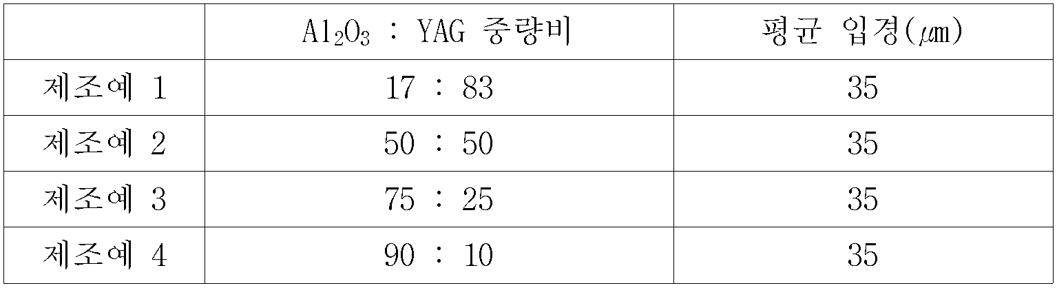
[제조예] Al2O3-YAG 복합산화물 분말의 제조Preparation Example Preparation of Al 2 O 3 -YAG Composite Oxide Powder
통상의 알려진 분무건조공정(단행본: Ceramic precusor technology and its applications, 저자: C.K. Narula, 출판사: M. Dekker (N.Y.) 출판년도: 1995)을 이용하여 하기 표 1에 나타낸 바와 같은 조성 및 평균입경을 갖는 Al2O3-YAG 복합산화물 분말을 제조하였다.Using a conventional known spray drying process (Paper: Ceramic precusor technology and its applications, Author: CK Narula, Publisher: M. Dekker (NY) Publication Year: 1995) has a composition and average particle size as shown in Table 1 below An Al 2 O 3 -YAG composite oxide powder was prepared.
[표 1]TABLE 1
[실시예 1 내지 4][Examples 1 to 4]
평판의 Al 모재(폭 100mm x 길이 100mm x 두께 5mm)의 한 면을 #100 Al2O3 입자를 이용하여 블라스팅 처리하여 표면거칠기(Ra: 2-3㎛)를 준 후, 그 표면의 전 면에 상기 제조예에서 제조된 서로 다른 조성을 갖는 4종의 Al2O3-YAG 복합산화물 분말을 사용하여 대기 플라즈마 용사법으로 500㎛ 두께로 유전층인 Al2O3-YAG계 코팅층을 형성하였다. Al2O3-YAG계 코팅층의 표면에 50mm x 50mm 면적부분을 전도성 전극층인 텅스텐을 대기 플라즈마 용사법으로 50㎛ 두께로 형성하였으며, 상기 플라즈마 열용사 후 코팅층의 실링처리는 하지 않았다. One surface of Al substrate (100mm wide x 100mm long x 5mm thick) of the plate was blasted using # 100 Al 2 O 3 particles to give a surface roughness (Ra: 2-3㎛), and then the front surface of the surface 4 Al 2 O 3 -YAG composite oxide powders having different compositions prepared in the above Preparation Example to form an Al 2 O 3 -YAG-based coating layer of a dielectric layer with a thickness of 500㎛ by atmospheric plasma spraying method. Tungsten, a conductive electrode layer, was formed on the surface of the Al 2 O 3 -YAG-based coating layer to a thickness of 50 μm by atmospheric plasma spraying, and the coating layer was not sealed after the plasma thermal spraying.
[비교예 1]Comparative Example 1
실시예 1과 동일한 방법으로 유전층 및 전도성 전극층을 형성하되, 유전층 형성시 Al2O3-YAG 복합산화물 분말 대신에 순도가 99.9wt%의 Al2O3 용사분말을 이용하여 500㎛ 두께의 유전층을 형성하였다. A dielectric layer and a conductive electrode layer are formed in the same manner as in Example 1, except that when the dielectric layer is formed, a dielectric layer having a thickness of 500 μm is formed using an Al 2 O 3 spray powder having a purity of 99.9 wt% instead of the Al 2 O 3 -YAG composite oxide powder. Formed.
상기 실시예 1 내지 4 및 비교예에서 제조된 시편을 이용하여 Al 모재와 텅스텐 코팅층의 양쪽에 직류전압을 인가하여 저항을 측정한 후 체적고유저항 값을 계산하였으며, 또한 0.5kV 단위로 인가전압을 증가시켜 코팅층의 절연파괴전압을 측정하였다. 상기 실험의 결과를 표 2에 나타내었다.Using the specimens prepared in Examples 1 to 4 and Comparative Examples, a DC voltage was applied to both the Al base material and the tungsten coating layer to measure the resistance, and then the volume specific resistance value was calculated, and the applied voltage was measured in units of 0.5 kV. By increasing the dielectric breakdown voltage of the coating layer was measured. The results of the experiment are shown in Table 2.
[표 2]TABLE 2

표 2에 나타낸 결과로부터 알 수 있는 바와 같이, 측정조건에 관계없이, 본 발명의 Al2O3-YAG계 코팅층은 종래의 Al2O3 코팅층보다 약 1000배 이상의 높은 체적고유저항과 높은 절연파괴전압을 나타내었다. 두 코팅층은 모두 습도에 민감한 전기적 절연 특성을 보였으며, 특히 Al2O3 코팅의 경우 1.5kV/mm 이하의 매우 낮은 전압인가에 대하여서도 큰 누설전류를 흘렸다. 즉, 도 3에 나타난 바와 같이, Al2O3 코팅층 내에 다량 포함되어 있는 미세한 기공 네트워크/채널은 주위로부터의 침투된 수분에 의하여 전도경로로 작용한다. 정전척이 사용되는 실제 환경은 전하를 띄는 플라즈마에 노출되어 있으므로, 상기 Al2O3 코팅층은 정전척의 유전층으로 사용할 수 없다. 반면에 Al2O3-YAG계 코팅층은 상기 표 1에 기재된 모든 조성에서 제한 된 기공 네트워크/채널로 인하여 습도가 높은 환경에서도 비교적 높은 절연파괴전압을 유지하고 있다.As can be seen from the results shown in Table 2, irrespective of the measurement conditions, the Al 2 O 3 -YAG coating layer of the present invention has a volume specific resistance and a high dielectric breakdown of about 1000 times higher than that of the conventional Al 2 O 3 coating layer. The voltage is shown. Both coating layers exhibited moisture-sensitive electrical insulation properties, especially for Al 2 O 3 coatings, which showed a large leakage current even at very low voltages below 1.5 kV / mm. That is, as shown in Figure 3, the fine pore network / channel contained in a large amount in the Al 2 O 3 coating layer acts as a conductive path by the moisture penetrated from the surroundings. Since the actual environment in which the electrostatic chuck is used is exposed to a charged plasma, the Al 2 O 3 coating layer cannot be used as the dielectric layer of the electrostatic chuck. On the other hand, Al 2 O 3 -YAG-based coating layer maintains a relatively high dielectric breakdown voltage even in a high humidity environment due to the limited pore network / channel in all compositions shown in Table 1.
[실시예 5 내지 8][Examples 5 to 8]
실시예 1 내지 4에서 형성한 상부 유전(절연)층의 표면에 유기계 액상 실링재를(Metcoseal ERS, Sulzer Metco Inc., USA) 도포한 후 진공에서 150℃에서 3시간 가열하는 실링처리를 더 진행한 것을 제외하고는 실시예 1 내지 4와 동일하게 유전층 및 전도성 전극층을 형성하였다.After applying the organic liquid sealing material (Metcoseal ERS, Sulzer Metco Inc., USA) to the surface of the upper dielectric (insulation) layer formed in Examples 1 to 4 and further subjected to a sealing treatment for heating for 3 hours at 150 ℃ in vacuum Except for the dielectric layer and the conductive electrode layer was formed in the same manner as in Examples 1 to 4.
[비교예 2] Comparative Example 2
실시예 5와 동일한 방법으로 실링처리된 유전층 및 전도성 전극층을 형성하되, 유전층을 Al2O3-YAG 복합산화물 분말 대신에 순도가 99.9wt%의 Al2O3 용사분말을 사용하였다.In the same manner as in Example 5, a sealed dielectric layer and a conductive electrode layer were formed, but instead of the Al 2 O 3 -YAG composite oxide powder, an Al 2 O 3 spray powder having a purity of 99.9 wt% was used.
표 3은 실링처리된 비교예 2의 Al2O3 코팅층과 실시예 2의 Al2O3-YAG계 코팅층의 전기적 절연특성을 나타낸 것이다. Table 3 shows the electrical insulation properties of the Al 2 O 3 coating layer of Comparative Example 2 and the Al 2 O 3 -YAG coating layer of Example 2 subjected to the sealing treatment.
[표 3]TABLE 3

종래의 Al2O3 플라즈마 코팅층의 경우 실링처리에 행함에 따라 크게 증가된 체적고유저항과 절연파괴전압을 나타내었으나, 실링처리를 행한 후에도 실링처리를 하지 않은 본 발명의 Al2O3-YAG계 코팅층과 비교하여 비슷한 값의 체적고유저항과 절연파괴전압을 나타내었다. 반면에 본 발명에 의한 실시예의 Al2O3-YAG계 코팅층은 표 1에 기재된 모든 조성에서 실링처리에 의하여 1 x 10¹⁵ Ω·㎝ 이상의 매우 높은 체적고유저항을 나타내었으며, ~44 kV/mm 이상의 매우 높은 직류전압 인가에도 절연파괴를 보이지 않았다. Conventional Al 2 O 3 Plasma coating layer showed the volume specific resistance and dielectric breakdown voltage greatly increased by the sealing treatment, but similar value compared to the Al 2 O 3 -YAG coating layer of the present invention which was not treated even after the sealing treatment. The volume specific resistance and dielectric breakdown voltage of are shown. On the other hand, Al 2 O 3 -YAG-based coating layer of the embodiment according to the present invention showed a very high volume specific resistance of 1 x 10 15 Ω · cm by the sealing treatment in all compositions shown in Table 1, ~ 44 kV / mm No insulation breakdown was observed even with the application of very high DC voltage.
[실시예 9]Example 9
실시예 9에서는 종래의 Al2O3 플라즈마 코팅층과 본 발명의 실시예에 따른 Al2O3·YAG계 플라즈마 코팅층의 실제 정전척으로의 적용에 따른 전기적 절연특성을 평가한 결과이다. 이를 위하여 직류전압을 인가할 수 있는 금속 전극봉이 포함된 축소된 크기(폭 100mm x 길이 120mm)의 Al 정전척 모재를 가공하였으며, 그 상부에 언더코트, 하부 절연(유전)층, 도전성 전극층, 상부 유전(절연)층을 플라즈마 용사법을 이용하여 순차적으로 적층하였다. 이때 도전성 전극층의 코팅 면적은 80mm x 100mm 이었다. 금속 전극봉은 중간의 전도성 전극층과 직접적으로 연결되며, 금속 전극봉 주위는 하부 절연(유전)층과 동일한 재료로 처리하여 Al 모재와 절연하였다. 언더코트로서는 100㎛ 두께의 Ni 코팅층을 형성하였으며, 전도성 전극층으로는 50㎛ 두께의 W 코팅층을 형성하였다. 비교예의 경우에는 하부 및 상부 유전(절연)층으로 순도가 99.9wt%의 Al2O3 코팅층을, 본 발명의 실시예의 경우에는 제조예 2의 Al2O3-YAG 복합산화물 분말(Al2O3:YAG 중량비 = 50:50, 평균입경 35㎛)을 사용하여 Al2O3-YAG계 코팅층을 각각 400㎛ 두께로 플라즈마 용사법을 이용하여 형성하였다. 플라즈마 코팅 완료 후, 상부 유전(절연)층의 표면에 에폭시계 액상 실링재(Metcoseal ERS, Sulzer Metco Inc., USA)를 도포한 후 진공에서 150℃에서 3시간 가열하는 실링처리를 행하였다.In Example 9, it is a result of evaluating the electrical insulation characteristics according to the application of the conventional Al 2 O 3 plasma coating layer and Al 2 O 3 · YAG plasma coating layer according to the embodiment of the present invention to the actual electrostatic chuck. To this end, a reduced size (100 mm x 120 mm) Al electrostatic chuck base material with a metal electrode capable of applying a DC voltage was processed, and an undercoat, a lower insulating (dielectric) layer, a conductive electrode layer, and an upper part were processed thereon. Dielectric (insulation) layers were sequentially deposited using plasma spraying. At this time, the coating area of the conductive electrode layer was 80mm x 100mm. The metal electrode was directly connected to the intermediate conductive electrode layer, and the metal electrode rod was insulated from the Al base material by treating with the same material as the lower insulating (dielectric) layer. As the undercoat, a Ni coating layer having a thickness of 100 μm was formed, and a W coating layer having a thickness of 50 μm was formed as the conductive electrode layer. In the comparative example, an Al 2 O 3 coating layer having a purity of 99.9 wt% was used as the lower and upper dielectric (insulation) layers, and in the embodiment of the present invention, Al 2 O 3 -YAG composite oxide powder (Al 2 O 3 : YAG weight ratio = 50:50, the average particle diameter of 35㎛) Al 2 O 3 -YAG-based coating layer was formed by the plasma spray method to each 400㎛ thickness. After the plasma coating was completed, an epoxy-based liquid sealing material (Metcoseal ERS, Sulzer Metco Inc., USA) was applied to the surface of the upper dielectric (insulation) layer, and then a sealing treatment was performed at 150 ° C. under vacuum for 3 hours.
상기 제조된 정전척의 전기적 특성을 평가하기 위하여, 대기 중에서 금속 전극봉에 0.5-5.0kV의 직류전압을 60초간 인가하여, 정전척의 누설전류 및 절연저항을 측정하였다.In order to evaluate the electrical characteristics of the manufactured electrostatic chuck, a DC voltage of 0.5-5.0 kV was applied to the metal electrode in the air for 60 seconds to measure leakage current and insulation resistance of the electrostatic chuck.
[표 4]TABLE 4

종래의 Al2O3 플라즈마 코팅층이 포함된 정전척은 인가전압의 증가와 함께 누설전류의 급격한 증가를 나타내었으며, 약 3.1kV의 인가전압에서 절연파괴 현상이 발생하였다. 반면에, 본 발명에 의한 Al2O3-YAG계 코팅층이 적용된 정전척은 동일한 인가전압에 대하여 Al2O3 정전척과 비교하여 약 5배 이상의 높은 절연저항을 나타내었으며, 인가전압의 증가에 따른 누설전류의 증가가 크지 않았다. 또한 상기 Al2O3-YAG계 코팅층이 적용된 정전척에 5.0kV의 직류전압을 10분간 이상 장시간 인가하더라도 유전(절연)층의 절연파괴가 발생하지 않았다. The electrostatic chuck including the conventional Al 2 O 3 plasma coating layer showed a sudden increase in leakage current with an increase in the applied voltage, and an insulation breakdown occurred at an applied voltage of about 3.1 kV. On the other hand, the electrostatic chuck to which the Al 2 O 3 -YAG-based coating layer according to the present invention is applied exhibits about 5 times higher insulation resistance than the Al 2 O 3 electrostatic chuck for the same applied voltage. The increase in leakage current was not large. In addition, even when a 5.0 kV DC voltage was applied for 10 minutes or more to the electrostatic chuck to which the Al 2 O 3 -YAG coating layer was applied, dielectric breakdown of the dielectric layer did not occur.
[실시예 10]Example 10
상기 실시예 9에서 축소된 크기의 정전척의 특성을 바탕으로, 실제 크기의 디스플레이패널 장비용 정전척(가로 1950mm x 세로 2150mm)을 실시예 9와 동일한 방법으로 제조하였으며, 정전척의 전기적 절연특성을 평가하였다. 종래의 Al2O3 열용사 코팅층이 적용된 정전척은 인가전압의 증가와 함께 누설전류가 크게 증가하였으며, 1-2kV 범위의 낮은 인가전압 하에서 아킹(arcing)이 발생하거나 절연파괴 됨으로써 정전척의 기능을 소실하였다. 반면에 본 발명의 Al2O3-YAG계 코팅층이 적용된 정전척의 경우, 인가전압 2.5-3.0kV에서 유리기판을 고정하기 위한 충분한 정전기력을 발생시켰으며, 그 이상의 전압에서도 절연파괴가 발생하지 않음과 동시에 허용된 범위의 누설전류를 나타내었다.Based on the characteristics of the reduced size of the electrostatic chuck in Example 9, an electrostatic chuck for display panel equipment (1950 mm x 2150 mm) was manufactured in the same manner as in Example 9, and the electrical insulation characteristics of the electrostatic chuck were evaluated. It was. In the conventional electrostatic chuck with Al 2 O 3 thermal spray coating layer, the leakage current increases greatly with the increase of the applied voltage, and arcing occurs or the dielectric breakdown is applied under the low applied voltage of 1-2kV, thereby preventing the function of the electrostatic chuck. It disappeared. On the other hand, in the case of the electrostatic chuck to which the Al 2 O 3 -YAG-based coating layer of the present invention is applied, sufficient electrostatic force is generated for fixing the glass substrate at an applied voltage of 2.5-3.0 kV, and no insulation breakdown occurs even at a higher voltage. At the same time, the leakage current in the allowed range was shown.
상술한 바와 같이 본 발명에 따르면, 열용사 코팅법을 이용한 정전척의 제조에 있어 체적고유저항과 절연파괴전압이 매우 큰 Al2O3-YAG계 코팅층을 하부 또는/및 상부 유전층에 적용함에 따라 정전척의 정전기력을 증가시킴과 동시에 내구성 및 수명을 크게 향상시킬 수 있다.As described above, according to the present invention, the electrostatic chuck using the thermal spray coating method is applied to the lower or / and the upper dielectric layer by applying an Al 2 O 3 -YAG-based coating layer having a very high volume specific resistance and dielectric breakdown voltage In addition to increasing the electrostatic force of the chuck, it can greatly improve the durability and service life.
또한 본 발명에 따르면 정전척을 구성하는 유전층을 Al2O3-YAG계 열용사 코팅층으로 형성하여 기공 네트워크 및 채널 생성이 억제됨으로써 외부로부터 코팅층 내로의 이종 오염 물질의 침입을 억제하고 실링재의 사용을 최소화할 수 있다.In addition, according to the present invention, the dielectric layer constituting the electrostatic chuck is formed of an Al 2 O 3 -YAG-based thermal spray coating layer to suppress pore network and channel generation, thereby suppressing the invasion of heterogeneous contaminants from the outside into the coating layer and using the sealing material. It can be minimized.
Claims (5)
Priority Applications (2)
| Application Number | Priority Date | Filing Date | Title |
|---|---|---|---|
| PCT/KR2007/000855 WO2008010632A1 (en) | 2006-07-20 | 2007-02-16 | Electrostatic chuck with high-resistivity ceramic coating materials |
| JP2009520666A JP4975101B2 (en) | 2006-07-20 | 2007-02-16 | High resistance ceramic thermal spray coating material and method for manufacturing electrostatic chuck including the same |
Applications Claiming Priority (2)
| Application Number | Priority Date | Filing Date | Title |
|---|---|---|---|
| KR1020060067754 | 2006-07-20 | ||
| KR20060067754 | 2006-07-20 |
Publications (2)
| Publication Number | Publication Date |
|---|---|
| KR20080008941A KR20080008941A (en) | 2008-01-24 |
| KR100877381B1 true KR100877381B1 (en) | 2009-01-09 |
Family
ID=39221673
Family Applications (1)
| Application Number | Title | Priority Date | Filing Date |
|---|---|---|---|
| KR1020070015622A Active KR100877381B1 (en) | 2006-07-20 | 2007-02-14 | High resistance ceramic thermal spray coating material and manufacturing method of electrostatic chuck including the same |
Country Status (2)
| Country | Link |
|---|---|
| JP (1) | JP4975101B2 (en) |
| KR (1) | KR100877381B1 (en) |
Families Citing this family (4)
| Publication number | Priority date | Publication date | Assignee | Title |
|---|---|---|---|---|
| KR102123912B1 (en) * | 2018-11-21 | 2020-06-18 | (주)제니스월드 | Manufacturing method of Electrostatic chuck using Surface Modified Method of Ceramic Coating Layer |
| CN113966544A (en) * | 2019-06-12 | 2022-01-21 | 朗姆研究公司 | Sealant coating for plasma processing chamber components |
| DE102022114212A1 (en) | 2021-06-09 | 2022-12-15 | Electronics And Telecommunications Research Institute | high voltage driving device |
| KR102843312B1 (en) * | 2023-12-08 | 2025-08-05 | 세메스 주식회사 | Substrate treating apparatus and manufacturing method thereof |
Citations (2)
| Publication number | Priority date | Publication date | Assignee | Title |
|---|---|---|---|---|
| KR20020070340A (en) * | 2000-01-21 | 2002-09-05 | 도카로 가부시키가이샤 | Electrostatic chuck member and method of producing the same |
| KR20060060612A (en) * | 2004-11-30 | 2006-06-05 | 가부시키가이샤 후지미인코퍼레이티드 | Thermal spraying powder, thermal spraying method and formation method of thermal spray coating |
Family Cites Families (3)
| Publication number | Priority date | Publication date | Assignee | Title |
|---|---|---|---|---|
| TW514996B (en) * | 1999-12-10 | 2002-12-21 | Tokyo Electron Ltd | Processing apparatus with a chamber having therein a high-corrosion-resistant sprayed film |
| KR100682740B1 (en) * | 2004-01-15 | 2007-02-15 | 주식회사 솔믹스 | Coating layer formation method of semiconductor manufacturing equipment |
| JP4467453B2 (en) * | 2004-09-30 | 2010-05-26 | 日本碍子株式会社 | Ceramic member and manufacturing method thereof |
-
2007
- 2007-02-14 KR KR1020070015622A patent/KR100877381B1/en active Active
- 2007-02-16 JP JP2009520666A patent/JP4975101B2/en active Active
Patent Citations (2)
| Publication number | Priority date | Publication date | Assignee | Title |
|---|---|---|---|---|
| KR20020070340A (en) * | 2000-01-21 | 2002-09-05 | 도카로 가부시키가이샤 | Electrostatic chuck member and method of producing the same |
| KR20060060612A (en) * | 2004-11-30 | 2006-06-05 | 가부시키가이샤 후지미인코퍼레이티드 | Thermal spraying powder, thermal spraying method and formation method of thermal spray coating |
Also Published As
| Publication number | Publication date |
|---|---|
| KR20080008941A (en) | 2008-01-24 |
| JP4975101B2 (en) | 2012-07-11 |
| JP2010515237A (en) | 2010-05-06 |
Similar Documents
| Publication | Publication Date | Title |
|---|---|---|
| JP4272786B2 (en) | Electrostatic chuck member and manufacturing method thereof | |
| KR100268052B1 (en) | Electrostatic chuck member and a method of producing the same | |
| TWI427188B (en) | Thermal spray powder, method for forming thermal spray coating, and plasma resistant member | |
| JP2009081223A (en) | Electrostatic chuck member | |
| KR20100101641A (en) | Electrostatic chuck and method of forming | |
| KR102266658B1 (en) | Yittrium granular powder for thermal spray and thermal spray coating produced using the same | |
| EP3792964B1 (en) | Electrostatic chuck and manufacturing method therefor | |
| KR20170141340A (en) | Sintered ceramics for electrostatic chuck and manufacturing method of the same | |
| KR100877381B1 (en) | High resistance ceramic thermal spray coating material and manufacturing method of electrostatic chuck including the same | |
| KR102356172B1 (en) | Method for Producing Plasma-Resistant Coating Layer | |
| KR101593078B1 (en) | Esd protection device and manufacturing method therefor | |
| US20070065678A1 (en) | Electro-static chuck with non-sintered aln and a method of preparing the same | |
| GB2583911A (en) | High density corrosion resistant layer arrangement for electrostatic chucks | |
| TW201942089A (en) | Composite sintered body, semiconductor manufacturing apparatus member, and method of manufacturing composite sintered body | |
| US5864459A (en) | Process for providing a glass dielectric layer on an electrically conductive substrate and electrostatic chucks made by the process | |
| JP4043219B2 (en) | Electrostatic chuck | |
| KR20100090559A (en) | Electrostatic chuck having aerosol coating layer and fabrication method thereof | |
| CN111081626A (en) | An electrostatic chuck containing high-resistance ceramic heat-spraying material | |
| WO2008010632A1 (en) | Electrostatic chuck with high-resistivity ceramic coating materials | |
| KR102721242B1 (en) | Base member for electrostatic chuck and method for preparing the same | |
| JP4510358B2 (en) | Electrostatic chuck and manufacturing method thereof | |
| US7525409B2 (en) | Method of manufacturing a varistor | |
| Nakashima et al. | Dielectric breakdown behavior of oxynitride glass | |
| KR100432639B1 (en) | Process for Providing a Glass-Ceramic Dielectric Layer on a Ceramic Substrate and Electrostatic Chuck Made by the Process | |
| RU2454841C2 (en) | Circuit substrate |
Legal Events
| Date | Code | Title | Description |
|---|---|---|---|
| A201 | Request for examination | ||
| PA0109 | Patent application |
St.27 status event code: A-0-1-A10-A12-nap-PA0109 |
|
| PA0201 | Request for examination |
St.27 status event code: A-1-2-D10-D11-exm-PA0201 |
|
| E902 | Notification of reason for refusal | ||
| PE0902 | Notice of grounds for rejection |
St.27 status event code: A-1-2-D10-D21-exm-PE0902 |
|
| PG1501 | Laying open of application |
St.27 status event code: A-1-1-Q10-Q12-nap-PG1501 |
|
| P11-X000 | Amendment of application requested |
St.27 status event code: A-2-2-P10-P11-nap-X000 |
|
| P13-X000 | Application amended |
St.27 status event code: A-2-2-P10-P13-nap-X000 |
|
| R18-X000 | Changes to party contact information recorded |
St.27 status event code: A-3-3-R10-R18-oth-X000 |
|
| E902 | Notification of reason for refusal | ||
| PE0902 | Notice of grounds for rejection |
St.27 status event code: A-1-2-D10-D21-exm-PE0902 |
|
| P11-X000 | Amendment of application requested |
St.27 status event code: A-2-2-P10-P11-nap-X000 |
|
| P13-X000 | Application amended |
St.27 status event code: A-2-2-P10-P13-nap-X000 |
|
| E701 | Decision to grant or registration of patent right | ||
| PE0701 | Decision of registration |
St.27 status event code: A-1-2-D10-D22-exm-PE0701 |
|
| GRNT | Written decision to grant | ||
| PR0701 | Registration of establishment |
St.27 status event code: A-2-4-F10-F11-exm-PR0701 |
|
| PR1002 | Payment of registration fee |
St.27 status event code: A-2-2-U10-U11-oth-PR1002 Fee payment year number: 1 |
|
| PG1601 | Publication of registration |
St.27 status event code: A-4-4-Q10-Q13-nap-PG1601 |
|
| R18-X000 | Changes to party contact information recorded |
St.27 status event code: A-5-5-R10-R18-oth-X000 |
|
| R18-X000 | Changes to party contact information recorded |
St.27 status event code: A-5-5-R10-R18-oth-X000 |
|
| R18-X000 | Changes to party contact information recorded |
St.27 status event code: A-5-5-R10-R18-oth-X000 |
|
| PR1001 | Payment of annual fee |
St.27 status event code: A-4-4-U10-U11-oth-PR1001 Fee payment year number: 4 |
|
| FPAY | Annual fee payment |
Payment date: 20121129 Year of fee payment: 5 |
|
| PR1001 | Payment of annual fee |
St.27 status event code: A-4-4-U10-U11-oth-PR1001 Fee payment year number: 5 |
|
| L13-X000 | Limitation or reissue of ip right requested |
St.27 status event code: A-2-3-L10-L13-lim-X000 |
|
| U15-X000 | Partial renewal or maintenance fee paid modifying the ip right scope |
St.27 status event code: A-4-4-U10-U15-oth-X000 |
|
| FPAY | Annual fee payment |
Payment date: 20131227 Year of fee payment: 6 |
|
| R18-X000 | Changes to party contact information recorded |
St.27 status event code: A-5-5-R10-R18-oth-X000 |
|
| PR1001 | Payment of annual fee |
St.27 status event code: A-4-4-U10-U11-oth-PR1001 Fee payment year number: 6 |
|
| FPAY | Annual fee payment |
Payment date: 20141201 Year of fee payment: 7 |
|
| PR1001 | Payment of annual fee |
St.27 status event code: A-4-4-U10-U11-oth-PR1001 Fee payment year number: 7 |
|
| R18-X000 | Changes to party contact information recorded |
St.27 status event code: A-5-5-R10-R18-oth-X000 |
|
| FPAY | Annual fee payment |
Payment date: 20151201 Year of fee payment: 8 |
|
| PR1001 | Payment of annual fee |
St.27 status event code: A-4-4-U10-U11-oth-PR1001 Fee payment year number: 8 |
|
| FPAY | Annual fee payment |
Payment date: 20161125 Year of fee payment: 9 |
|
| PR1001 | Payment of annual fee |
St.27 status event code: A-4-4-U10-U11-oth-PR1001 Fee payment year number: 9 |
|
| P22-X000 | Classification modified |
St.27 status event code: A-4-4-P10-P22-nap-X000 |
|
| FPAY | Annual fee payment |
Payment date: 20171122 Year of fee payment: 10 |
|
| PR1001 | Payment of annual fee |
St.27 status event code: A-4-4-U10-U11-oth-PR1001 Fee payment year number: 10 |
|
| PR1001 | Payment of annual fee |
St.27 status event code: A-4-4-U10-U11-oth-PR1001 Fee payment year number: 11 |
|
| FPAY | Annual fee payment |
Payment date: 20191202 Year of fee payment: 12 |
|
| PR1001 | Payment of annual fee |
St.27 status event code: A-4-4-U10-U11-oth-PR1001 Fee payment year number: 12 |
|
| PR1001 | Payment of annual fee |
St.27 status event code: A-4-4-U10-U11-oth-PR1001 Fee payment year number: 13 |
|
| R18-X000 | Changes to party contact information recorded |
St.27 status event code: A-5-5-R10-R18-oth-X000 |
|
| PR1001 | Payment of annual fee |
St.27 status event code: A-4-4-U10-U11-oth-PR1001 Fee payment year number: 14 |
|
| PN2301 | Change of applicant |
St.27 status event code: A-5-5-R10-R11-asn-PN2301 |
|
| PN2301 | Change of applicant |
St.27 status event code: A-5-5-R10-R14-asn-PN2301 |
|
| P14-X000 | Amendment of ip right document requested |
St.27 status event code: A-5-5-P10-P14-nap-X000 |
|
| PR1001 | Payment of annual fee |
St.27 status event code: A-4-4-U10-U11-oth-PR1001 Fee payment year number: 15 |
|
| PR1001 | Payment of annual fee |
St.27 status event code: A-4-4-U10-U11-oth-PR1001 Fee payment year number: 16 |
|
| PR1001 | Payment of annual fee |
St.27 status event code: A-4-4-U10-U11-oth-PR1001 Fee payment year number: 17 |
|
| PN2301 | Change of applicant |
St.27 status event code: A-5-5-R10-R13-asn-PN2301 St.27 status event code: A-5-5-R10-R11-asn-PN2301 |
|
| R11 | Change to the name of applicant or owner or transfer of ownership requested |
Free format text: ST27 STATUS EVENT CODE: A-5-5-R10-R11-ASN-PN2301 (AS PROVIDED BY THE NATIONAL OFFICE) |
|
| R13 | Change to the name of applicant or owner recorded |
Free format text: ST27 STATUS EVENT CODE: A-5-5-R10-R13-ASN-PN2301 (AS PROVIDED BY THE NATIONAL OFFICE) |
|
| PR1001 | Payment of annual fee |
St.27 status event code: A-4-4-U10-U11-oth-PR1001 Fee payment year number: 18 |
|
| U11 | Full renewal or maintenance fee paid |
Free format text: ST27 STATUS EVENT CODE: A-4-4-U10-U11-OTH-PR1001 (AS PROVIDED BY THE NATIONAL OFFICE) Year of fee payment: 18 |
|
| P22-X000 | Classification modified |
St.27 status event code: A-4-4-P10-P22-nap-X000 |