KR100871389B1 - Fuse of Semiconductor Device and Formation Method - Google Patents
Fuse of Semiconductor Device and Formation Method Download PDFInfo
- Publication number
- KR100871389B1 KR100871389B1 KR1020070100223A KR20070100223A KR100871389B1 KR 100871389 B1 KR100871389 B1 KR 100871389B1 KR 1020070100223 A KR1020070100223 A KR 1020070100223A KR 20070100223 A KR20070100223 A KR 20070100223A KR 100871389 B1 KR100871389 B1 KR 100871389B1
- Authority
- KR
- South Korea
- Prior art keywords
- fuse
- film
- region
- forming
- semiconductor device
- Prior art date
- Legal status (The legal status is an assumption and is not a legal conclusion. Google has not performed a legal analysis and makes no representation as to the accuracy of the status listed.)
- Expired - Fee Related
Links
Images


Classifications
-
- H10W20/494—
Landscapes
- Internal Circuitry In Semiconductor Integrated Circuit Devices (AREA)
- Design And Manufacture Of Integrated Circuits (AREA)
Abstract
Description
본 발명은 반도체 소자의 퓨즈 및 그의 형성방법에 관한 것으로, 보다 상세하게는, 공정 마진(Margin)을 개선하고 리페어 효율을 향상시킬 수 있는 반도체 소자의 퓨즈 및 그의 형성방법에 관한 것이다.BACKGROUND OF THE INVENTION 1. Field of the Invention The present invention relates to a fuse of a semiconductor device and a method of forming the same, and more particularly, to a fuse of a semiconductor device and a method of forming the same that can improve process margins and improve repair efficiency.
최근, 컴퓨터와 같은 정보 매체의 급속한 보급에 따라 반도체 장치도 비약적으로 발전하고 있다. 그 기능 면에 있어서, 반도체 장치는 고속으로 동작하는 동시에 대용량의 저장 능력을 가질 것이 요구된다. 이에 따라, 반도체 장치는 집적도, 신뢰도 및 응답 속도 등을 향상시키는 방향으로 제조 기술이 발전되고 있다.In recent years, with the rapid spread of information media such as computers, semiconductor devices are also rapidly developing. In terms of its function, the semiconductor device is required to operate at a high speed and to have a large storage capacity. Accordingly, the manufacturing technology of semiconductor devices has been developed to improve the degree of integration, reliability, and response speed.
반도체 장치는 주로 실리콘 재질의 기판 상에 설정된 회로 패턴을 반복적으로 형성하여 집적 회로를 갖는 셀들을 형성하는 패브리케이션(Fabrication : FAB) 공정과, 상기 셀들이 형성된 기판을 칩(Chip) 단위로 패키징(Packaging)하는 어셈블리(Assembly) 공정을 포함한다. 그리고, 상기 패브리케이션 공정과 어셈블리 공정 사이에는 상기 기판 상에 형성하는 셀들의 전기적 특성을 검사하기 위한 공정(Electrical Die Sorting : EDS)을 수행한다.A semiconductor device mainly includes a fabrication (FAB) process of repeatedly forming a circuit pattern set on a silicon substrate to form cells having an integrated circuit, and packaging the substrate on which the cells are formed in a chip unit (Chip). Packaging and assembly process. In addition, a process for inspecting electrical characteristics of cells formed on the substrate is performed between the fabrication process and the assembly process.
상기 검사 공정은 기판 상에 형성한 셀들이 전기적으로 양호한 상태 또는 불량한 상태를 갖는가를 판별하는 공정이다. 이는, 상기 검사 공정을 통하여 불량한 상태를 갖는 셀들을 상기 어셈블리 공정을 수행하기 이전에 제거함으로서, 상기 어셈블리 공정에서 소모되는 노력 및 비용을 절감하기 위함이다. 그리고, 상기 불량한 상태를 갖는 셀들을 조기에 발견하고, 이를 리페어(Repair) 공정을 통하여 재생하기 위함이다.The inspection step is a step of determining whether the cells formed on the substrate have an electrically good state or a bad state. This is to reduce the effort and cost consumed in the assembly process by removing the cells having a bad state through the inspection process before performing the assembly process. In order to detect the cells having the defective state at an early stage and regenerate them through a repair process.
여기서, 상기 리페어 공정에 대해 좀더 자세히 설명하면 다음과 같다.Here, the repair process will be described in more detail as follows.
반도체 소자 제조 공정 중 결함이 발생할 경우 소자의 수율을 향상시킬 목적으로 소자 설계시 결함있는 소자 또는 회로를 대체하기 위하여 여분(Redundancy)의 셀을 부가하며, 이러한 여분의 셀을 집적회로에 접속시키기 위해 퓨즈를 함께 설계하고 있는데, 상기 리페어 공정은 검사공정을 통해 불량으로 판명된 셀을 상기 퓨즈를 사용하여 칩 내에 내장된 여분의 셀과 연결시켜 재생시키는 공정이다. 즉, 특정 퓨즈들만을 커팅(Cutting)함으로써 리페어할 셀들의 위치 정보를 생성하는 것이다.Redundancy cells are added to replace defective devices or circuits in the design of devices for the purpose of improving the yield of devices in the event of defects in the semiconductor device manufacturing process, and to connect these redundant cells to integrated circuits. The fuse is designed together, and the repair process is a process in which a cell, which has been found to be defective through an inspection process, is connected to a spare cell embedded in a chip using the fuse to be regenerated. That is, by cutting only specific fuses, location information of cells to be repaired is generated.
이하에서는, 종래 기술에 따른 반도체 소자의 리페어 방법을 간략하게 설명하도록 한다.Hereinafter, a repair method of a semiconductor device according to the prior art will be briefly described.
먼저, 반도체 기판의 퓨즈 영역 상에 표면이 평탄화된 층간절연막을 증착한 후, 상기 층간절연막 상에 다수의 퓨즈들을 형성한다. 상기 퓨즈들은 균일한 폭과 두께를 갖는 라인 타입으로 형성되며, 통상, 퓨즈 영역의 단차 및 공정 마진의 개선을 위해 금속막으로 형성한다. First, an interlayer insulating film having a flattened surface is deposited on a fuse area of a semiconductor substrate, and then a plurality of fuses are formed on the interlayer insulating film. The fuses are formed in a line type having a uniform width and thickness, and are generally formed of a metal film in order to improve the step area and the process margin of the fuse area.
그런 다음, 상기 퓨즈들을 덮도록 반도체 기판의 결과물 상에 절연막과 보호막을 차례로 증착한다. 이어서, 상기 보호막과 절연막의 일부 두께를 리페어 식각하여 블로윙 예정 영역에 형성된 퓨즈 상에 소정 두께의 절연막을 잔류시키는 리페어용 트렌치를 형성한다.Then, an insulating film and a protective film are sequentially deposited on the resultant of the semiconductor substrate so as to cover the fuses. Subsequently, a partial thickness of the passivation layer and the insulating layer is repair-etched to form a trench for repairing an insulating layer having a predetermined thickness on the fuse formed in the blown region.
그리고 나서, 상기 리페어용 트렌치가 형성된 반도체 기판의 퓨즈 영역에 레이저를 조사하여 특정 퓨즈를 커팅하는 퓨즈 블로윙(Blowing) 공정을 포함하는 공지의 검사 및 리페어 공정을 차례로 수행한다.Then, a known inspection and repair process including a fuse blowing process of cutting a specific fuse by irradiating a laser to a fuse region of the semiconductor substrate on which the repair trench is formed is sequentially performed.
그러나, 전술한 종래 기술의 경우에는, 반도체 소자의 낮은 저항을 구현하기 위하여 상기 금속막으로 형성된 퓨즈를 두꺼운 두께를 형성하기 때문에 퓨즈를 커팅하는 데에 많은 에너지가 필요하며, 이로 인해, 퓨즈 불로윙 공정시 퓨즈 자체에 많은 스트레스가 가해질 뿐 아니라 그에 인접한 다른 퓨즈에까지 스트레스가 가해지는 등 페일(Fail)이 유발된다.However, in the above-described prior art, a large amount of energy is required to cut the fuse because the fuse formed of the metal film forms a thick thickness in order to realize a low resistance of the semiconductor device. In the process, a large amount of stress is applied to the fuse itself, and a stress is applied to another fuse adjacent thereto.
그러므로, 이와 같은 페일 없이 최적의 리페어 효율을 얻기 위한 퓨즈의 크기, 리페어용 트렌치 하부에 잔류된 절연막의 두께, 리페어 공정시의 레이저 스팟 크기와 에너지 조건 등을 조절하는 데에 한계가 있으며, 그 결과, 공정 마진이 감소하고 리페어 효율이 저하된다.Therefore, there is a limit in controlling the size of the fuse to obtain the optimal repair efficiency without the fail, the thickness of the insulating film remaining under the repair trench, the laser spot size and energy conditions during the repair process, and the result. This reduces process margins and reduces repair efficiency.
본 발명은 공정 마진(Margin)을 개선하고 리페어 효율을 향상시킬 수 있는 반도체 소자의 퓨즈 및 그의 형성방법을 제공한다.The present invention provides a fuse of a semiconductor device and a method of forming the same that can improve process margins and improve repair efficiency.
본 발명에 따른 반도체 소자의 퓨즈는, 블로윙 영역을 포함한 퓨즈 영역을 갖는 반도체 기판; 상기 반도체 기판 상에 형성된 식각정지막; 상기 식각 정지막 상에 형성되며, 상기 블로윙 영역 양측의 퓨즈 영역 부분에 배치된 다수의 도전 패턴; 상기 블로윙 영역과 이에 인접한 도전 패턴 부분이 노출되도록 형성된 절연막; 및 상기 절연막 및 식각 정지막 상에 상기 노출된 도전 패턴 부분과 콘택하도록 형성되며, 상기 블로윙 영역에서 상기 블로윙 영역의 양측보다 얇은 두께를 갖는 퓨즈 라인;을 포함한다.A fuse of a semiconductor device according to the present invention includes a semiconductor substrate having a fuse region including a blowing region; An etch stop layer formed on the semiconductor substrate; A plurality of conductive patterns formed on the etch stop layer and disposed on portions of the fuse region on both sides of the blowing region; An insulating layer formed to expose the blowing region and a portion of the conductive pattern adjacent thereto; And a fuse line formed on the insulating layer and the etch stop layer to contact the exposed conductive pattern portion, the fuse line having a thickness thinner than both sides of the blowing region in the blowing region.
여기서, 상기 퓨즈 라인은 상기 블로윙 영역에서 상기 블로윙 영역의 퓨즈 라인 두께의 50∼200%의 폭을 갖는다.Here, the fuse line has a width of 50 to 200% of the fuse line thickness of the blowing region in the blowing region.
상기 퓨즈 라인은 표면 상에 베리어막을 구비한다.The fuse line has a barrier film on its surface.
상기 베리어막은 Ti막, 또는, TiN막으로 이루어진다.The barrier film is made of a Ti film or a TiN film.
상기 퓨즈 라인은 금속막으로 이루어진다.The fuse line is made of a metal film.
상기 금속막은 알루미늄막이다.The metal film is an aluminum film.
또한, 본 발명에 따른 반도체 소자의 퓨즈 형성방법은, 블로윙 영역을 포함한 퓨즈 영역을 갖는 반도체 기판 상에 식각정지막을 형성하는 단계; 상기 식각정지막 상에 절연막을 형성하는 단계; 상기 절연막을 식각하여 상기 블로윙 영역을 포함한 퓨즈 영역의 식각정지막 부분을 노출시키는 트렌치를 형성하는 단계; 상기 트렌치를 매립하도록 상기 절연막 상에 도전막을 형성하는 단계; 및 상기 도전막을 식각하여 상기 블로윙 영역이 상기 블로윙 영역 양측의 나머지 퓨즈 영역보다 얇은 두께를 갖는 퓨즈 라인을 형성하는 단계;를 포함한다.In addition, a fuse forming method of a semiconductor device according to the present invention may include forming an etch stop layer on a semiconductor substrate having a fuse region including a blowing region; Forming an insulating film on the etch stop film; Etching the insulating layer to form a trench for exposing an etch stop layer portion of the fuse region including the blowing region; Forming a conductive film on the insulating film to fill the trench; And etching the conductive layer to form a fuse line having a thickness smaller than that of the remaining fuse regions on both sides of the blowing region.
여기서, 상기 식각정지막은 질화막으로 형성한다.Here, the etch stop film is formed of a nitride film.
상기 트렌치를 형성하는 단계 후, 그리고, 상기 트렌치를 매립하도록 도전막을 형성하는 단계 전, 상기 트렌치의 표면을 포함한 절연막 상에 베리어막을 형성 하는 단계;를 더 포함한다.And forming a barrier film on the insulating film including the surface of the trench after forming the trench and before forming the conductive film to fill the trench.
상기 베리어막은 Ti막, 또는, TiN막으로 형성한다.The barrier film is formed of a Ti film or a TiN film.
상기 도전막은 금속막으로 형성한다.The conductive film is formed of a metal film.
상기 금속막은 알루미늄막이다.The metal film is an aluminum film.
상기 퓨즈 라인은 상기 블로윙 영역에서 상기 블로윙 영역의 퓨즈 라인 두께의 50∼200%의 폭을 갖도록 형성한다.The fuse line is formed to have a width of 50 to 200% of a thickness of the fuse line of the blowing region in the blowing region.
본 발명은 식각정지막 상에 금속막을 증착하고 상기 금속막의 과도 식각(Over Etch)량을 조절하여 퓨즈 라인을 형성함으로써, 퓨즈 라인의 블로윙 영역 부분이 리페어 공정에 적합한 두께를 갖도록 효과적으로 조절할 수 있으며, 이를 통해, 리페어 효율을 향상시킬 수 있다.According to the present invention, by forming a fuse line by depositing a metal film on the etch stop layer and adjusting the over-etch amount of the metal film, the blowing area portion of the fuse line can be effectively adjusted to have a thickness suitable for the repair process. Through this, the repair efficiency can be improved.
또한, 본 발명은 상기 퓨즈 라인을 셀 영역의 금속 배선 형성시 과도 식각량을 조절하면서 함께 형성함으로써, 공정 조건을 변화시키지 않고 추가되는 공정 없이 리페어 공정에 적합한 두께의 퓨즈 라인을 형성할 수 있으므로, 공정 마진을 개선할 수 있다.In addition, according to the present invention, by forming the fuse line while controlling the excessive etching amount when forming the metal wiring of the cell region, it is possible to form a fuse line having a thickness suitable for the repair process without changing the process conditions without additional process, Process margins can be improved.
이하에서는, 첨부된 도면을 참조하여 본 발명의 바람직한 실시예를 상세하게 설명하도록 한다. Hereinafter, with reference to the accompanying drawings will be described in detail a preferred embodiment of the present invention.
도 1은 본 발명의 실시예에 따른 반도체 소자의 퓨즈를 설명하기 위한 단면도이다.1 is a cross-sectional view illustrating a fuse of a semiconductor device in accordance with an embodiment of the present invention.
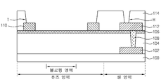
도 1에 도시된 바와 같이, 블로윙 영역을 포함한 퓨즈 영역과 셀 영역을 가지며, 상기 셀 영역에 제1금속 배선(102)이 형성된 반도체 기판(100) 상에 상기 제1금속 배선(102)을 덮도록 제1절연막(104)이 형성된다. 상기 제1절연막 (104)상에 식각정지막(106)이 형성된다. 상기 블로윙 영역 양측 퓨즈 영역 부분의 식각정지막(106) 상에 다수개의 도전 패턴(110)이 형성됨과 아울러 상기 셀 영역의 식각정지막(106) 상에 제2금속 배선(112)이 형성된다. 그리고, 상기 제1 및 제2금속 배선(106, 112)을 콘택시키는 제1콘택 플러그(108)가 형성된다. 상기 도전 패턴(110) 및 제2금속 배선(112)이 형성된 반도체 기판(100) 상에 제2절연막(114)이 형성되며, 상기 제2절연막(114)은 블로윙 영역과 이에 인접한 도전 패턴(110) 부분이 노출되도록 형성된다.
상기 제2절연막(114) 및 식각정지막(106) 상에 상기 노출된 도전 패턴(110) 부분과 콘택함과 아울러, 블로윙 영역에서 상기 블로윙 영역 양측보다 얇은 두께를 갖는 퓨즈 라인(FL)이 형성되며, 상기 셀 영역의 제2금속 배선(112) 상에 제2콘택 플러그(122)와 제3금속배선(124)이 형성된다.As shown in FIG. 1, the
A fuse line FL is formed on the second insulating
삭제delete
또한, 상기 퓨즈 라인(FL)은 상기 블로윙 영역 부분에서 상기 블로윙 영역의 퓨즈 라인(FL) 두께의 50∼200%의 폭을 갖도록 형성되며, 그 표면 상에 Ti막, 또는, TiN막으로 이루어진 제1 및 제2베리어막(116, 120)을 구비한다. 또한, 상기 퓨즈 라인(FL)은 상기 제3금속배선(124)과 동일한 재질의 금속막, 예컨데, 알루미늄막으로 이루어진다.In addition, the fuse line FL is formed to have a width of 50 to 200% of the thickness of the fuse line FL of the blowing region in the blowing region, and is formed of a Ti film or a TiN film on the surface thereof. And first and
여기서, 본 발명은 상기 퓨즈 라인(FL)이 상기 블로윙 영역 부분이 블로윙 영역 양측의 나머지 퓨즈 영역 부분보다 얇은 두께로 형성되기 때문에 상기 퓨즈 라인(FL)이 리페어 공정시 적합합 형태를 가지며, 이를 통해, 리페어 효율을 개선할 수 있고 공정 마진을 향상시킬 수 있다. Here, since the fuse line FL is formed to have a thickness thinner than that of the fuse area on both sides of the blowing area, the fuse line FL has a form suitable for a repair process. As a result, repair efficiency can be improved and process margins can be improved.
도 2a 내지 도 2g는 본 발명의 실시예에 따른 반도체 소자의 퓨즈 형성방법을 설명하기 위한 공정별 단면도이다.2A through 2G are cross-sectional views illustrating processes of forming a fuse of a semiconductor device according to an exemplary embodiment of the present invention.
도 2a를 참조하면, 블로윙 영역을 포함한 퓨즈 영역과 셀 영역을 갖는 반도체 기판(100) 상에 소정의 하부 구조물(도시 안됨)들을 형성한 후, 상기 셀 영역에 제1금속배선(102)을 형성한다. 그리고 나서, 상기 하부 구조물들과 제1금속 배선(102)을 덮도록, 예컨데, 산화막으로 제1절연막(104)을 증착한다. Referring to FIG. 2A, after forming predetermined lower structures (not shown) on a
그런 다음, 상기 제1절연막(104)의 표면을 평탄화함이 바람직하며, 상기 평탄화된 각 영역의 제1절연막(104) 상에 식각정지막(106)을 형성한다. 상기 식각정지막(106)은 상기 제1절연막(104)과 식각 선택비를 갖는 막, 예컨데, 질화막으로 형성한다. Then, the surface of the first insulating
도 2b를 참조하면, 상기 식각정지막(106) 상에 도전막, 바람직하게는, 금속막을 증착하고, 그리고 나서, 상기 금속막을 패터닝하여 상기 반도체 기판(100)의 셀 영역에 제2금속 배선(112)을 형성함과 아울러 퓨즈 영역에 다수의 도전 패턴(110)을 형성한다. 한편, 상기 셀 영역의 제1절연막(104)과 식각정지막(106) 내에 상기 제2금속 배선(112)과 상기 제1금속 배선(102)을 콘택시키는 제1콘택 플러그(108)를 형성함이 바람직하다.Referring to FIG. 2B, a conductive film, preferably a metal film, is deposited on the
도 2c를 참조하면, 상기 도전 패턴(110)과 제2금속배선(112)을 덮도록 반도체 기판(100) 각 영역의 식각정지막(106) 상에 제2절연막(114)을 증착한 다음, 상기 제2절연막(114)의 표면을 평탄화함이 바람직하다.Referring to FIG. 2C, a second insulating
도 2d를 참조하면, 상기 제2절연막(114)을 식각하여 퓨즈 영역에 제1도전 패 턴 부분 및 그 사이의 식각정지막 부분을 노출시키는 트렌치(T)를 형성함과 아울러 셀 영역에 제2금속 배선(112)을 노출시키는 콘택홀(H)을 형성한다. 이때, 상기 트렌치(T)는 상기 블로윙 영역을 포함한 블로윙 영역 양측의 퓨즈 영역 부분에 형성한다.Referring to FIG. 2D, the second insulating
도 2e를 참조하면, 상기 콘택홀(H)과 트렌치(T)의 표면을 포함한 제2절연막(114) 상에 제1베리어막(116)을 형성한 후, 상기 제1베리어막(116) 상에 콘택홀(H)과 트렌치(T)를 매립하도록 도전막, 바람직하게는, 금속막(118)을 형성한다. 이어서, 상기 금속막(118) 상에 제2베리어막(120)을 형성한다. 상기 제1 및 제2베리어막(116, 120)은 Ti막, 또는, TiN막으로 형성함이 바람직하며, 상기 금속막(118)은 알루미늄막으로 형성함이 바람직하다.Referring to FIG. 2E, after the
도 2f를 참조하면, 상기 제2베리어막(120)과 금속막(118) 및 제1베리어막(116)을 식각하여 퓨즈 영역에 도전 패턴(110)과 콘택하며 블로윙 영역 부분이 상기 블로윙 영역 양측 부분보다 얇은 두께를 갖는 퓨즈 라인(FL)을 형성함과 아울러 셀 영역에 제2금속 배선(112)과 콘택하는 제3금속 배선(124)을 형성한다. 이때, 상기 제2금속 배선(112)과 제3금속 배선(124)을 콘택시키는 제2콘택 플러그(122)도 함께 형성함이 바람직하다. 또한, 상기 퓨즈 라인(FL)은 상기 블로윙 영역 부분에서 상기 블로윙 영역의 퓨즈 라인(FL) 두께의 50∼200%의 폭을 갖도록 형성한다.Referring to FIG. 2F, the
여기서, 본 발명은 식각정지막(106) 상에 형성된 금속막(118)의 과도 식각(Over Etch)량을 조절하여 퓨즈 라인(FL)을 형성함으로써, 상기 퓨즈 라인(FL)의 블로윙 영역 부분이 리페어 공정에 적합한 얇은 두께를 갖도록 효과적으로 조절할 수 있으며, 이를 통해, 리페어 효율을 향상시킬 수 있다.Here, the present invention forms the fuse line FL by adjusting the over-etch amount of the
도 2g를 참조하면, 상기 퓨즈 라인(FL)과 제3금속 배선(124)이 형성된 반도체 기판(100)의 각 영역 상에 제3절연막(126)과 보호막(128)을 차례로 형성한 다음, 퓨즈 영역의 보호막(128)과 제3절연막(126)의 일부 두께를 식각하여 퓨즈 라인(FL)의 블로윙 영역 상에 소정 두께의 제3절연막(126)을 잔류시키는 리페어용 트렌치(RT)를 형성한다.Referring to FIG. 2G, a third
이후, 도시하지는 않았지만 상기 리페어용 트렌치(RT)가 형성된 반도체 기판(100)의 퓨즈 영역에 레이저를 조사하여 특정 퓨즈 라인(FL)을 커팅하는 퓨즈 블로윙(Blowing) 공정을 포함하는 공지의 검사 및 리페어 공정을 차례로 수행한다.Subsequently, although not shown, a known inspection and repair including a fuse blowing process of cutting a specific fuse line FL by irradiating a laser to a fuse region of the
한편, 전술한 본 발명의 실시예에서는 상기 퓨즈 라인을 셀 영역의 제2금속배선과 동일 레이어로 형성하는 방법에 대하여 도시하고 설명하였으나, 상기 퓨즈 라인은 제1금속 배선이나 제3금속 배선 등의 다른 금속 배선과 동일 레이어로 형성할 수도 있다. Meanwhile, in the above-described embodiment of the present invention, a method of forming the fuse line in the same layer as the second metal wiring of the cell region is illustrated and described. However, the fuse line may include the first metal wiring, the third metal wiring, or the like. It can also be formed in the same layer as other metal wiring.
또한, 전술한 본 발명의 실시예에서는 상기 퓨즈 라인과 외부 회로를 콘택시키는 역할을 하는 도전 패턴으로서 제2금속 배선과 동일 레이어로 형성되는 도전 패턴을 도시하고 설명하였으나, 상기 도전 패턴은 제1금속 배선이나 제3금속 배선 등의 다른 금속 배선과 동일 레이어로 형성하는 것도 가능하다.In addition, in the above-described embodiment of the present invention, as the conductive pattern serving to contact the fuse line and the external circuit, the conductive pattern formed of the same layer as the second metal wiring is illustrated and described. It is also possible to form the same layer as other metal wirings, such as a wiring and a 3rd metal wiring.
여기서, 본 발명은 식각정지막 상에 형성된 금속막의 과도 식각량을 조절하면서 상기 금속막을 식각함으로써, 블로윙 영역 부분이 리페어 공정시 적합하도록 얇은 두께를 갖는 퓨즈 라인을 형성할 수 있으며, 따라서, 본 발명은 리페어 효율 을 효과적으로 개선할 수 있다.Here, the present invention can form a fuse line having a thin thickness so that the blowing region portion is suitable for the repair process by etching the metal film while controlling the excessive etching amount of the metal film formed on the etch stop film, and thus, the present invention Can effectively improve the repair efficiency.
또한, 본 발명은 상기 퓨즈 라인을 셀 영역의 금속 배선 형성시 퓨즈 영역의 금속막 과도 식각량을 조절하면서 함께 형성함으로써, 공정 조건을 변화시키지 않고 추가되는 공정 없이 리페어 공정에 적합한 두께의 퓨즈 라인을 형성할 수 있으므로, 공정 마진을 개선할 수 있다.In addition, the present invention is to form a fuse line having a thickness suitable for the repair process without changing the process conditions by forming the fuse line while controlling the excessive etching amount of the metal film of the fuse region when forming the metal wiring of the cell region. Since it can form, process margin can be improved.
이상, 여기에서는 본 발명을 특정 실시예에 관련하여 도시하고 설명하였지만, 본 발명이 그에 한정되는 것은 아니며, 이하의 특허청구의 범위는 본 발명의 정신과 분야를 이탈하지 않는 한도 내에서 본 발명이 다양하게 개조 및 변형될 수 있다는 것을 당업계에서 통상의 지식을 가진 자가 용이하게 알 수 있다.As mentioned above, although the present invention has been illustrated and described with reference to specific embodiments, the present invention is not limited thereto, and the following claims are not limited to the scope of the present invention without departing from the spirit and scope of the present invention. It can be easily understood by those skilled in the art that can be modified and modified.
도 1은 본 발명의 실시예에 따른 반도체 소자의 퓨즈를 설명하기 위한 단면도.1 is a cross-sectional view illustrating a fuse of a semiconductor device according to an embodiment of the present invention.
도 2a 내지 도 2g는 본 발명의 실시예에 따른 반도체 소자의 퓨즈를 설명하기 위한 공정별 단면도.2A to 2G are cross-sectional views illustrating processes of a fuse of a semiconductor device in accordance with an embodiment of the present invention.
* 도면의 주요 부분에 대한 부호의 설명 *Explanation of symbols on the main parts of the drawings
100 : 반도체 기판 102 : 제1금속 배선100
104 : 제1절연막 106 : 식각정지막104: first insulating film 106: etch stop film
108 : 제1콘택 플러그 110 : 도전 패턴108: first contact plug 110: conductive pattern
112 : 제2금속 배선 114 : 제2절연막112: second metal wiring 114: second insulating film
T : 트렌치 H : 콘택홀T: Trench H: Contact Hole
116 : 제1베리어막 118 : 금속막116: first barrier film 118: metal film
120 : 제2베리어막 122 : 제2콘택 플러그120: second barrier film 122: the second contact plug
124 : 제3금속 배선 126 : 제3절연막124: third metal wiring 126: third insulating film
128 : 보호막 RT : 리페어용 트렌치128: protective film RT: trench for repair
Claims (13)
Priority Applications (1)
| Application Number | Priority Date | Filing Date | Title |
|---|---|---|---|
| KR1020070100223A KR100871389B1 (en) | 2007-10-05 | 2007-10-05 | Fuse of Semiconductor Device and Formation Method |
Applications Claiming Priority (1)
| Application Number | Priority Date | Filing Date | Title |
|---|---|---|---|
| KR1020070100223A KR100871389B1 (en) | 2007-10-05 | 2007-10-05 | Fuse of Semiconductor Device and Formation Method |
Publications (1)
| Publication Number | Publication Date |
|---|---|
| KR100871389B1 true KR100871389B1 (en) | 2008-12-02 |
Family
ID=40371709
Family Applications (1)
| Application Number | Title | Priority Date | Filing Date |
|---|---|---|---|
| KR1020070100223A Expired - Fee Related KR100871389B1 (en) | 2007-10-05 | 2007-10-05 | Fuse of Semiconductor Device and Formation Method |
Country Status (1)
| Country | Link |
|---|---|
| KR (1) | KR100871389B1 (en) |
Cited By (2)
| Publication number | Priority date | Publication date | Assignee | Title |
|---|---|---|---|---|
| KR100972917B1 (en) | 2007-12-26 | 2010-08-03 | 주식회사 하이닉스반도체 | Semiconductor device and method of forming the same |
| KR101178567B1 (en) * | 2010-12-16 | 2013-05-14 | 에스케이하이닉스 주식회사 | Fuse in semiconductor device and method for fabrication the same |
Citations (4)
| Publication number | Priority date | Publication date | Assignee | Title |
|---|---|---|---|---|
| JP2002110799A (en) | 2000-09-27 | 2002-04-12 | Toshiba Corp | Semiconductor device and manufacturing method thereof |
| KR20060001193A (en) * | 2004-06-30 | 2006-01-06 | 주식회사 하이닉스반도체 | Method for forming fuse part of semiconductor device |
| KR20070060355A (en) * | 2005-12-08 | 2007-06-13 | 주식회사 하이닉스반도체 | Fuse Formation Method of Semiconductor Device |
| KR20070077382A (en) * | 2006-01-23 | 2007-07-26 | 주식회사 하이닉스반도체 | Fuse Formation Method of Semiconductor Device |
-
2007
- 2007-10-05 KR KR1020070100223A patent/KR100871389B1/en not_active Expired - Fee Related
Patent Citations (4)
| Publication number | Priority date | Publication date | Assignee | Title |
|---|---|---|---|---|
| JP2002110799A (en) | 2000-09-27 | 2002-04-12 | Toshiba Corp | Semiconductor device and manufacturing method thereof |
| KR20060001193A (en) * | 2004-06-30 | 2006-01-06 | 주식회사 하이닉스반도체 | Method for forming fuse part of semiconductor device |
| KR20070060355A (en) * | 2005-12-08 | 2007-06-13 | 주식회사 하이닉스반도체 | Fuse Formation Method of Semiconductor Device |
| KR20070077382A (en) * | 2006-01-23 | 2007-07-26 | 주식회사 하이닉스반도체 | Fuse Formation Method of Semiconductor Device |
Cited By (3)
| Publication number | Priority date | Publication date | Assignee | Title |
|---|---|---|---|---|
| KR100972917B1 (en) | 2007-12-26 | 2010-08-03 | 주식회사 하이닉스반도체 | Semiconductor device and method of forming the same |
| US7973341B2 (en) | 2007-12-26 | 2011-07-05 | Hynix Semiconductor Inc. | Fuse of semiconductor device |
| KR101178567B1 (en) * | 2010-12-16 | 2013-05-14 | 에스케이하이닉스 주식회사 | Fuse in semiconductor device and method for fabrication the same |
Similar Documents
| Publication | Publication Date | Title |
|---|---|---|
| KR100871389B1 (en) | Fuse of Semiconductor Device and Formation Method | |
| KR20120103982A (en) | Fuse pattern and method for manufacturing the same | |
| CN113394193B (en) | Semiconductor structure and forming method thereof, and fusing method of laser fuse | |
| KR100728964B1 (en) | Fuse of Semiconductor Device and Formation Method | |
| KR101150554B1 (en) | Semiconductor Device and Method for Manufacturing the same | |
| KR101052873B1 (en) | Fuse box of semiconductor device and repair method using same | |
| KR101102048B1 (en) | Fuse of semiconductor device and manufacturing method thereof | |
| KR100929627B1 (en) | Fuse box of semiconductor device and forming method thereof | |
| KR20110065753A (en) | Manufacturing Method of Semiconductor Device | |
| KR100570065B1 (en) | Manufacturing method of semiconductor device | |
| KR20090103499A (en) | Method for repair of semiconductor device | |
| KR100876897B1 (en) | Fuse of Semiconductor Device and Formation Method | |
| KR20070041111A (en) | Fuse Formation Method of Semiconductor Device | |
| KR20120126440A (en) | Semiconductor Device and Method for Manufacturing the same | |
| KR100833588B1 (en) | Manufacturing method of semiconductor device | |
| KR20080081551A (en) | Repair method of semiconductor device | |
| KR20070048404A (en) | Fuses in Semiconductor Devices | |
| KR20070041113A (en) | Manufacturing method of semiconductor device | |
| KR20080002504A (en) | Repair method of semiconductor device | |
| KR20080027078A (en) | Fuse box of semiconductor device and forming method thereof | |
| KR20080029704A (en) | Method for forming fuse box of semiconductor device | |
| KR20110025476A (en) | Semiconductor device and manufacturing method thereof | |
| KR20100036013A (en) | Fuse box of semiconductor device and method for forming the same | |
| KR20080010995A (en) | Fuse box of semiconductor device and forming method thereof | |
| KR20080028543A (en) | Fuse box of semiconductor device and forming method thereof |
Legal Events
| Date | Code | Title | Description |
|---|---|---|---|
| A201 | Request for examination | ||
| PA0109 | Patent application |
St.27 status event code: A-0-1-A10-A12-nap-PA0109 |
|
| PA0201 | Request for examination |
St.27 status event code: A-1-2-D10-D11-exm-PA0201 |
|
| D13-X000 | Search requested |
St.27 status event code: A-1-2-D10-D13-srh-X000 |
|
| D14-X000 | Search report completed |
St.27 status event code: A-1-2-D10-D14-srh-X000 |
|
| E902 | Notification of reason for refusal | ||
| PE0902 | Notice of grounds for rejection |
St.27 status event code: A-1-2-D10-D21-exm-PE0902 |
|
| P11-X000 | Amendment of application requested |
St.27 status event code: A-2-2-P10-P11-nap-X000 |
|
| P13-X000 | Application amended |
St.27 status event code: A-2-2-P10-P13-nap-X000 |
|
| E701 | Decision to grant or registration of patent right | ||
| PE0701 | Decision of registration |
St.27 status event code: A-1-2-D10-D22-exm-PE0701 |
|
| GRNT | Written decision to grant | ||
| PR0701 | Registration of establishment |
St.27 status event code: A-2-4-F10-F11-exm-PR0701 |
|
| PR1002 | Payment of registration fee |
St.27 status event code: A-2-2-U10-U11-oth-PR1002 Fee payment year number: 1 |
|
| PG1601 | Publication of registration |
St.27 status event code: A-4-4-Q10-Q13-nap-PG1601 |
|
| LAPS | Lapse due to unpaid annual fee | ||
| PC1903 | Unpaid annual fee |
St.27 status event code: A-4-4-U10-U13-oth-PC1903 Not in force date: 20111126 Payment event data comment text: Termination Category : DEFAULT_OF_REGISTRATION_FEE |
|
| PN2301 | Change of applicant |
St.27 status event code: A-5-5-R10-R13-asn-PN2301 St.27 status event code: A-5-5-R10-R11-asn-PN2301 |
|
| PC1903 | Unpaid annual fee |
St.27 status event code: N-4-6-H10-H13-oth-PC1903 Ip right cessation event data comment text: Termination Category : DEFAULT_OF_REGISTRATION_FEE Not in force date: 20111126 |
|
| PN2301 | Change of applicant |
St.27 status event code: A-5-5-R10-R13-asn-PN2301 St.27 status event code: A-5-5-R10-R11-asn-PN2301 |
|
| PN2301 | Change of applicant |
St.27 status event code: A-5-5-R10-R13-asn-PN2301 St.27 status event code: A-5-5-R10-R11-asn-PN2301 |
|
| P22-X000 | Classification modified |
St.27 status event code: A-4-4-P10-P22-nap-X000 |
|
| P22-X000 | Classification modified |
St.27 status event code: A-4-4-P10-P22-nap-X000 |
|
| P22-X000 | Classification modified |
St.27 status event code: A-4-4-P10-P22-nap-X000 |