KR100869804B1 - Light emitting device and display device - Google Patents
Light emitting device and display device Download PDFInfo
- Publication number
- KR100869804B1 KR100869804B1 KR1020070066582A KR20070066582A KR100869804B1 KR 100869804 B1 KR100869804 B1 KR 100869804B1 KR 1020070066582 A KR1020070066582 A KR 1020070066582A KR 20070066582 A KR20070066582 A KR 20070066582A KR 100869804 B1 KR100869804 B1 KR 100869804B1
- Authority
- KR
- South Korea
- Prior art keywords
- electrodes
- electron emission
- light emitting
- substrate
- emitting device
- Prior art date
- Legal status (The legal status is an assumption and is not a legal conclusion. Google has not performed a legal analysis and makes no representation as to the accuracy of the status listed.)
- Expired - Fee Related
Links
Images


Classifications
-
- H—ELECTRICITY
- H01—ELECTRIC ELEMENTS
- H01J—ELECTRIC DISCHARGE TUBES OR DISCHARGE LAMPS
- H01J1/00—Details of electrodes, of magnetic control means, of screens, or of the mounting or spacing thereof, common to two or more basic types of discharge tubes or lamps
- H01J1/02—Main electrodes
- H01J1/30—Cold cathodes, e.g. field-emissive cathode
- H01J1/304—Field-emissive cathodes
-
- G—PHYSICS
- G02—OPTICS
- G02F—OPTICAL DEVICES OR ARRANGEMENTS FOR THE CONTROL OF LIGHT BY MODIFICATION OF THE OPTICAL PROPERTIES OF THE MEDIA OF THE ELEMENTS INVOLVED THEREIN; NON-LINEAR OPTICS; FREQUENCY-CHANGING OF LIGHT; OPTICAL LOGIC ELEMENTS; OPTICAL ANALOGUE/DIGITAL CONVERTERS
- G02F1/00—Devices or arrangements for the control of the intensity, colour, phase, polarisation or direction of light arriving from an independent light source, e.g. switching, gating or modulating; Non-linear optics
- G02F1/01—Devices or arrangements for the control of the intensity, colour, phase, polarisation or direction of light arriving from an independent light source, e.g. switching, gating or modulating; Non-linear optics for the control of the intensity, phase, polarisation or colour
- G02F1/13—Devices or arrangements for the control of the intensity, colour, phase, polarisation or direction of light arriving from an independent light source, e.g. switching, gating or modulating; Non-linear optics for the control of the intensity, phase, polarisation or colour based on liquid crystals, e.g. single liquid crystal display cells
- G02F1/133—Constructional arrangements; Operation of liquid crystal cells; Circuit arrangements
- G02F1/1333—Constructional arrangements; Manufacturing methods
- G02F1/1335—Structural association of cells with optical devices, e.g. polarisers or reflectors
- G02F1/1336—Illuminating devices
- G02F1/133602—Direct backlight
-
- H—ELECTRICITY
- H01—ELECTRIC ELEMENTS
- H01J—ELECTRIC DISCHARGE TUBES OR DISCHARGE LAMPS
- H01J63/00—Cathode-ray or electron-stream lamps
- H01J63/02—Details, e.g. electrode, gas filling, shape of vessel
-
- H—ELECTRICITY
- H01—ELECTRIC ELEMENTS
- H01J—ELECTRIC DISCHARGE TUBES OR DISCHARGE LAMPS
- H01J63/00—Cathode-ray or electron-stream lamps
- H01J63/06—Lamps with luminescent screen excited by the ray or stream
-
- H—ELECTRICITY
- H01—ELECTRIC ELEMENTS
- H01J—ELECTRIC DISCHARGE TUBES OR DISCHARGE LAMPS
- H01J9/00—Apparatus or processes specially adapted for the manufacture, installation, removal, maintenance of electric discharge tubes, discharge lamps, or parts thereof; Recovery of material from discharge tubes or lamps
- H01J9/24—Manufacture or joining of vessels, leading-in conductors or bases
- H01J9/32—Sealing leading-in conductors
-
- G—PHYSICS
- G02—OPTICS
- G02F—OPTICAL DEVICES OR ARRANGEMENTS FOR THE CONTROL OF LIGHT BY MODIFICATION OF THE OPTICAL PROPERTIES OF THE MEDIA OF THE ELEMENTS INVOLVED THEREIN; NON-LINEAR OPTICS; FREQUENCY-CHANGING OF LIGHT; OPTICAL LOGIC ELEMENTS; OPTICAL ANALOGUE/DIGITAL CONVERTERS
- G02F1/00—Devices or arrangements for the control of the intensity, colour, phase, polarisation or direction of light arriving from an independent light source, e.g. switching, gating or modulating; Non-linear optics
- G02F1/01—Devices or arrangements for the control of the intensity, colour, phase, polarisation or direction of light arriving from an independent light source, e.g. switching, gating or modulating; Non-linear optics for the control of the intensity, phase, polarisation or colour
- G02F1/13—Devices or arrangements for the control of the intensity, colour, phase, polarisation or direction of light arriving from an independent light source, e.g. switching, gating or modulating; Non-linear optics for the control of the intensity, phase, polarisation or colour based on liquid crystals, e.g. single liquid crystal display cells
- G02F1/133—Constructional arrangements; Operation of liquid crystal cells; Circuit arrangements
- G02F1/1333—Constructional arrangements; Manufacturing methods
- G02F1/1335—Structural association of cells with optical devices, e.g. polarisers or reflectors
- G02F1/1336—Illuminating devices
- G02F1/133625—Electron stream lamps
Landscapes
- Physics & Mathematics (AREA)
- Nonlinear Science (AREA)
- Engineering & Computer Science (AREA)
- Manufacturing & Machinery (AREA)
- Mathematical Physics (AREA)
- Chemical & Material Sciences (AREA)
- Crystallography & Structural Chemistry (AREA)
- General Physics & Mathematics (AREA)
- Optics & Photonics (AREA)
- Cathode-Ray Tubes And Fluorescent Screens For Display (AREA)
Abstract
본 발명은 고전압 안정성을 높일 수 있는 발광 장치 및 이 발광 장치를 광원으로 사용하는 표시 장치를 제공한다. 본 발명에 의한 발광 장치는 서로 대향 배치되는 제1 기판 및 제2 기판과, 제1 기판의 일면에 위치하며 복수의 전자 방출 소자들로 구성되는 전자 방출 유닛과, 제2 기판의 일면에 위치하며 가시광을 방출하는 발광 유닛을 포함한다. 그리고 각각의 전자 방출 소자는 제1 기판의 일 방향을 따라 서로간 거리를 두고 위치하는 제1 전극들과, 일 방향을 따라 제1 전극들 사이에 위치하는 제2 전극들과, 제1 전극들에 전기적으로 연결되며 제1 전극들보다 낮은 높이로 형성되는 제1 전자 방출부들을 포함한다.The present invention provides a light emitting device capable of increasing high voltage stability and a display device using the light emitting device as a light source. The light emitting device according to the present invention includes a first substrate and a second substrate disposed to face each other, an electron emission unit comprising a plurality of electron emission elements on one surface of the first substrate, and on one surface of the second substrate. And a light emitting unit for emitting visible light. Each of the electron emission devices may include first electrodes positioned at a distance from each other along one direction of the first substrate, second electrodes positioned between the first electrodes along one direction, and first electrodes. First electron emitters electrically connected to the first electron emitters, the first electron emitters being formed at a lower height than the first electrodes.
Description
도 1은 본 발명의 제1 실시예에 따른 발광 장치의 부분 단면도이다.1 is a partial cross-sectional view of a light emitting device according to a first embodiment of the present invention.
도 2는 도 1에 도시한 전자 방출 유닛의 부분 평면도이다.FIG. 2 is a partial plan view of the electron emission unit shown in FIG. 1.
도 3은 도 2에 도시한 전자 방출 소자의 사시도이다.3 is a perspective view of the electron emission device illustrated in FIG. 2.
도 4는 도 2에 표기한 Ⅱ-Ⅱ선의 단면도이다.4 is a cross-sectional view taken along the line II-II shown in FIG. 2.
도 5는 본 발명의 제2 실시예에 따른 발광 장치의 부분 단면도이다.5 is a partial cross-sectional view of a light emitting device according to a second embodiment of the present invention.
도 6은 도 5에 도시한 전자 방출 유닛의 부분 평면도이다.FIG. 6 is a partial plan view of the electron emission unit shown in FIG. 5.
도 7은 도 6에 도시한 전자 방출 소자의 사시도이다.FIG. 7 is a perspective view of the electron emission device illustrated in FIG. 6.
도 8과 도 9는 본 발명의 제2 실시예에 따른 발광 장치의 부분 단면도이다.8 and 9 are partial cross-sectional views of a light emitting device according to a second embodiment of the present invention.
도 10a 내지 도 10d는 본 발명의 제2 실시예에 따른 발광 장치 중 전자 방출 소자의 첫 번째 제조 방법을 나타낸 부분 단면도이다.10A to 10D are partial cross-sectional views showing a first manufacturing method of an electron emitting device of a light emitting device according to a second embodiment of the present invention.
도 11a 내지 도 11e는 본 발명의 제2 실시예에 따른 발광 장치 중 전자 방출 소자의 두 번째 제조 방법을 나타낸 부분 단면도이다.11A to 11E are partial cross-sectional views showing a second manufacturing method of the electron emitting device of the light emitting device according to the second embodiment of the present invention.
도 12는 본 발명의 제1 실시예 또는 제2 실시예의 발광 장치를 광원으로 사용하는 본 발명의 일 실시예에 따른 표시 장치의 분해 사시도이다.12 is an exploded perspective view of a display device according to an exemplary embodiment in which the light emitting device of the first or second exemplary embodiment of the present invention is used as a light source.
도 13은 도 12에 도시한 표시 패널의 부분 단면도이다.FIG. 13 is a partial cross-sectional view of the display panel shown in FIG. 12.
<도면의 주요 부분에 대한 참조 부호의 설명><Description of reference numerals for the main parts of the drawings>
100, 101: 발광 장치 16, 161: 전자 방출 유닛100, 101:
18: 발광 유닛 20, 201: 전자 방출 소자18:
22: 제1 전극 24: 제2 전극22: first electrode 24: second electrode
26: 전자 방출부 34: 애노드 전극26
36: 형광층 38: 금속 반사막36: fluorescent layer 38: metal reflective film
40: 제2 전자 방출부 42, 421: 희생층40: second
50: 표시 패널 52: 확산판50: display panel 52: diffusion plate
본 발명은 발광 장치에 관한 것으로서, 보다 상세하게는 전자 방출 유닛의 구조를 개선한 발광 장치 및 이 발광 장치를 광원으로 사용하는 표시 장치에 관한 것이다.The present invention relates to a light emitting device, and more particularly, to a light emitting device having an improved structure of an electron emitting unit and a display device using the light emitting device as a light source.
외부에서 볼 때 광이 출사된다는 것을 인식할 수 있는 모든 장치를 발광 장치라 하면, 전면 기판에 형광층과 애노드 전극을 구비하고, 후면 기판에 전자 방출부와 구동 전극을 구비한 발광 장치가 공지되어 있다. 전면 기판과 후면 기판은 밀봉 부재에 의해 가장자리가 일체로 접합된 후 내부 공간이 배기되어 밀봉 부재와 함께 진공 용기를 구성한다.When all devices capable of recognizing that light is emitted from the outside are light emitting devices, a light emitting device having a fluorescent layer and an anode electrode on a front substrate and an electron emission part and a driving electrode on a rear substrate is known. have. After the front substrate and the rear substrate are integrally bonded to each other by the sealing member, the inner space is exhausted to form a vacuum container together with the sealing member.
구동 전극은 서로간 거리를 두고 나란히 위치하는 캐소드 전극과 게이트 전극으로 이루어지며, 전자 방출부는 게이트 전극을 향한 캐소드 전극의 측면에 위치 한다. 구동 전극과 전자 방출부가 전자 방출 유닛을 구성한다.The driving electrode includes a cathode electrode and a gate electrode positioned side by side with a distance from each other, the electron emission portion is located on the side of the cathode electrode toward the gate electrode. The drive electrode and the electron emitting portion constitute the electron emitting unit.
발광 장치는 캐소드 전극과 게이트 전극에 소정의 구동 전압을 인가하고, 애노드 전극에 수천 볼트 이상의 양의 직류 전압(애노드 전압)을 인가하여 구동한다. 그러면 캐소드 전극과 게이트 전극의 전압 차에 의해 전자 방출부 주위에 전계가 형성되어 이로부터 전자들이 방출되고, 방출된 전자들이 애노드 전압에 이끌려 대응하는 형광층에 충돌함으로써 이를 발광시킨다.The light emitting device applies a predetermined driving voltage to the cathode electrode and the gate electrode, and drives the anode by applying a direct current voltage (anode voltage) of several thousand volts or more to the anode electrode. Then, an electric field is formed around the electron emission part by the voltage difference between the cathode electrode and the gate electrode, and electrons are emitted therefrom, and the emitted electrons are attracted by the anode voltage and collide with the corresponding fluorescent layer to emit light.
전술한 발광 장치에서 발광면의 휘도는 애노드 전압에 비례하므로 애노드 전압을 높여 휘도 향상을 도모하게 된다. 그런데 전술한 발광 장치에서는 전자 방출부가 애노드 전계의 영향을 직접적으로 받기 때문에, 애노드 전압이 높아질수록 전자 방출부 주위로 애노드 전계가 강화되며, 애노드 전계에 의해 전자가 오방출되는 다이오드 에미션이 발생하게 된다.In the above-described light emitting device, since the luminance of the light emitting surface is proportional to the anode voltage, the anode voltage is increased to improve the luminance. However, in the above-described light emitting device, since the electron emitter is directly affected by the anode electric field, the anode field is strengthened around the electron emitter as the anode voltage increases, so that diode emission in which electrons are mis-emitted by the anode electric field is generated. do.
또한, 전술한 발광 장치에서는 진공 용기 내부의 잔류 기체나 내부 구조물 표면의 전하 차징 등으로 인해 애노드 전압이 높아질수록 진공 용기 내부에 아크 방전이 일어날 가능성이 높아진다. 이와 같이 종래의 발광 장치는 고압 안정성이 낮으며, 애노드 전압을 높이는데 한계가 있으므로 휘도 향상에 어려움이 있다.In addition, in the above-described light emitting device, as the anode voltage is increased due to residual gas in the vacuum chamber or charge charging on the surface of the internal structure, the possibility of arc discharge in the vacuum chamber increases. As described above, the light emitting device of the related art has a low high voltage stability and has a limitation in increasing the anode voltage, thus making it difficult to improve luminance.
또한, 캐소드 전극과 게이트 전극은 스퍼터링 또는 진공 증착과 같은 이른바 박막 공정에 의해 형성되는 것이 일반적인데, 박막 공정에 의해 형성된 전극은 비교적 높은 저항을 가진다. 따라서 발광 장치 작용시 구동 전극에 전압 강하가 발생하며, 전압 강하로 인해 발광면의 휘도 균일도가 저하될 수 있다.In addition, the cathode electrode and the gate electrode are generally formed by a so-called thin film process such as sputtering or vacuum deposition, and the electrode formed by the thin film process has a relatively high resistance. Therefore, a voltage drop occurs in the driving electrode when the light emitting device operates, and the luminance uniformity of the light emitting surface may decrease due to the voltage drop.
따라서 본 발명은 상기한 문제점을 해소하기 위한 것으로서, 본 발명은 고압 안정성을 높여서 아크 방전을 억제하고 애노드 전압을 높여서 발광면의 휘도를 향상시킬 수 있는 발광 장치 및 이 발광 장치를 광원으로 사용하는 표시 장치를 제공하고자 한다.Therefore, the present invention is to solve the above problems, the present invention is to increase the stability of the high pressure to suppress the arc discharge, to increase the anode voltage to improve the brightness of the light emitting surface and display using the light emitting device as a light source To provide a device.
본 발명의 일 실시예에 따른 발광 장치는 서로 대향 배치되는 제1 기판 및 제2 기판과, 제1 기판의 일면에 위치하며 복수의 전자 방출 소자들로 구성되는 전자 방출 유닛과, 제2 기판의 일면에 위치하며 가시광을 방출하는 발광 유닛을 포함하고, 각각의 전자 방출 소자는 제1 기판의 일 방향을 따라 서로간 거리를 두고 위치하는 제1 전극들과, 상기 일 방향을 따라 제1 전극들 사이에 위치하는 제2 전극들과, 제1 전극들에 전기적으로 연결되며 제1 전극들보다 낮은 높이로 형성되는 제1 전자 방출부들을 포함한다.According to an exemplary embodiment, a light emitting device includes a first substrate and a second substrate disposed to face each other, an electron emission unit disposed on one surface of the first substrate, and configured of a plurality of electron emission devices, and a second substrate. A light emitting unit is disposed on one surface and emits visible light. Each of the electron emission devices includes first electrodes positioned at a distance from each other along one direction of the first substrate, and first electrodes along the one direction. Second electrodes disposed between the first electrodes and first electron emitters electrically connected to the first electrodes and formed at a lower height than the first electrodes.
제1 전극들과 제1 전자 방출부들은 1 내지 10㎛의 높이 차이를 가질 수 있으며, 제1 전극들과 제2 전극들은 30 내지 200㎛의 간격을 두고 위치할 수 있다.The first electrodes and the first electron emission parts may have a height difference of 1 to 10 μm, and the first electrodes and the second electrodes may be positioned at an interval of 30 to 200 μm.
전자 방출 소자는 제2 전극들에 전기적으로 연결되면서 제2 전극들보다 낮은 높이로 형성되는 제2 전자 방출부들을 더욱 포함할 수 있다. 이때, 제2 전극들과 제2 전자 방출부들은 1 내지 10㎛의 높이 차이를 가질 수 있으며, 제1 전자 방출부들과 제2 전자 방출부들은 3 내지 20㎛의 간격을 두고 위치할 수 있다.The electron emission device may further include second electron emission portions that are electrically connected to the second electrodes and are formed at a lower height than the second electrodes. In this case, the second electrodes and the second electron emitters may have a height difference of 1 to 10 μm, and the first electron emitters and the second electron emitters may be disposed at an interval of 3 to 20 μm.
제1 전극들과 제2 전극들은 제1 기간에서 주사 구동 전압과 데이터 구동 전압을 각각 인가받고, 제2 기간에서 데이터 구동 전압과 주사 구동 전압을 각각 인 가받을 수 있다. 제1 전자 방출부들과 제2 전자 방출부들은 카바이드 유도 탄소를 포함할 수 있다.The first electrodes and the second electrodes may receive the scan driving voltage and the data driving voltage in the first period, and the data driving voltage and the scan driving voltage in the second period, respectively. The first electron emitters and the second electron emitters may include carbide derived carbon.
본 발명의 일 실시예에 따른 표시 장치는 영상을 표시하는 표시 패널과, 표시 패널로 빛을 제공하는 발광 장치를 포함하며, 발광 장치는 서로 대향 배치되는 제1 기판 및 제2 기판과, 제1 기판의 일면에 위치하며 복수의 전자 방출 소자들로 구성되는 전자 방출 유닛과, 제2 기판의 일면에 위치하며 가시광을 방출하는 발광 유닛을 포함한다. 각각의 전자 방출 소자는 제1 기판의 일 방향을 따라 서로간 거리를 두고 위치하는 제1 전극들과, 상기 일 방향을 따라 제1 전극들 사이에 위치하는 제2 전극들과, 제1 전극들에 전기적으로 연결되며 제1 전극들보다 낮은 높이로 형성되는 제1 전자 방출부들을 포함한다.A display device according to an embodiment of the present invention includes a display panel for displaying an image, a light emitting device for providing light to the display panel, the light emitting device comprising: a first substrate and a second substrate facing each other, and a first An electron emission unit is disposed on one surface of the substrate and includes a plurality of electron emission elements, and a light emission unit is disposed on one surface of the second substrate to emit visible light. Each of the electron emission devices may include first electrodes positioned at a distance from each other along one direction of the first substrate, second electrodes positioned between the first electrodes along the one direction, and first electrodes. First electron emitters electrically connected to the first electron emitters, the first electron emitters being formed at a lower height than the first electrodes.
표시 패널이 제1 화소들을 형성할 때, 발광 장치는 제1 화소들보다 적은 개수의 제2 화소들을 형성하며, 각각의 제2 화소는 대응하는 제1 화소들의 계조에 대응하여 독립적으로 발광할 수 있다. 제2 화소마다 하나의 전자 방출 소자가 위치할 수 있으며, 표시 패널은 액정 표시 패널일 수 있다.When the display panel forms the first pixels, the light emitting device forms a smaller number of second pixels than the first pixels, and each second pixel may independently emit light corresponding to the gray levels of the corresponding first pixels. have. One electron emission device may be positioned for each second pixel, and the display panel may be a liquid crystal display panel.
이하, 첨부한 도면을 참고로 하여 본 발명의 실시예에 대하여 본 발명이 속하는 기술 분야에서 통상의 지식을 가진 자가 용이하게 실시할 수 있도록 상세히 설명한다. 본 발명은 여러 가지 상이한 형태로 구현될 수 있으며 여기에서 설명하는 실시예에 한정되지 않는다.Hereinafter, exemplary embodiments of the present invention will be described in detail with reference to the accompanying drawings so that those skilled in the art may easily implement the present invention. As those skilled in the art would realize, the described embodiments may be modified in various different ways, all without departing from the spirit or scope of the present invention.
도 1은 본 발명의 제1 실시예에 따른 발광 장치의 부분 단면도이고, 도 2는 도 1에 도시한 전자 방출 유닛의 부분 평면도이며, 도 3은 도 2에 도시한 전자 방 출 소자의 사시도이다.1 is a partial cross-sectional view of a light emitting device according to a first embodiment of the present invention, FIG. 2 is a partial plan view of the electron emission unit shown in FIG. 1, and FIG. 3 is a perspective view of the electron emission device shown in FIG. .
도 1 내지 도 3을 참고하면, 본 실시예의 발광 장치(100)는 소정의 간격을 두고 평행하게 대향 배치되는 제1 기판(12)과 제2 기판(14)을 포함한다. 제1 기판(12)과 제2 기판(14)의 가장자리에는 밀봉 부재(도시하지 않음)가 배치되어 이 기판들(12, 14)을 접합시키며, 내부 공간이 대략 10-6 Torr의 진공도로 배기되어 제1 기판(12)과 제2 기판(14) 및 밀봉 부재가 진공 용기를 구성한다.1 to 3, the
제1 기판(12)과 제2 기판(14) 중 밀봉 부재의 내측에 위치하는 영역은 실제 가시광 방출에 기여하는 유효 영역과, 유효 영역을 둘러싸는 비유효 영역으로 구분지을 수 있다. 제1 기판(12) 내면의 유효 영역에는 전자 방출을 위한 전자 방출 유닛(16)이 위치하고, 제2 기판(14) 내면의 유효 영역에는 가시광 방출을 위한 발광 유닛(18)이 위치한다.The region located inside the sealing member of the
발광 유닛(18)이 위치하는 제2 기판(14)이 발광 장치(100)의 전면 기판이 될 수 있으며, 전자 방출 유닛(16)이 위치하는 제1 기판(12)이 발광 장치(100)의 후면 기판이 될 수 있다.The
본 실시예에서 전자 방출 유닛(16)은 다음에 설명하는 구조와 구동 방법에 의해 방출 전류량이 독립적으로 제어되는 복수의 전자 방출 소자들(20)로 이루어진다.In the present embodiment, the
각각의 전자 방출 소자(20)는 제1 기판(12)의 일 방향(도면의 y축 방향)을 따라 서로간 거리를 두고 위치하는 제1 전극들(22)과, 상기 일 방향을 따라 제1 전 극들(22) 사이에 위치하는 제2 전극들(24)과, 제2 전극들(24)을 향한 제1 전극들(22)의 측면에 위치하며 제1 전극(22)보다 낮은 높이로 형성되는 전자 방출부들(26)을 포함한다. 제1 전극들(22)과 제2 전극들(24)은 서로 나란하게 위치한다.Each of the
제1 전극(22)은 전자 방출부(26)에 전류를 공급하는 캐소드 전극이 되고, 제2 전극(24)은 제1 전극(22)과의 전압 차에 의해 전자 방출부(26) 주위에 전계를 형성하여 전자 방출을 유도하는 게이트 전극이 된다. 전자 방출부(26)는 제1 전극들(22)의 길이 방향을 따라 형성되며, 제2 전극들(24)과 쇼트되지 않도록 제2 전극들(24)과 일정한 거리를 두고 위치한다.The
제1 전극들(22)의 일측 단부에는 제1 연결 전극(221)이 위치하여 제1 전극들(22)과 함께 제1 전극 세트(222)를 구성하고, 제2 전극들(24)의 일측 단부에는 제2 연결 전극(241)이 위치하여 제2 전극들(24)과 함께 제2 전극 세트(242)를 구성한다.The
제1 전극들(22)과 제2 전극들(24)은 전자 방출부(26)보다 큰 높이로 형성된다. 이를 위해 제1 전극들(22)과 제2 전극들(24)은 스퍼터링 또는 진공 증착과 같은 박막 공정이 아닌 스크린 인쇄 또는 라미네이팅과 같은 이른바 후막 공정으로 형성된다.The
전자 방출부(26)는 진공 중에서 전계가 가해지면 전자를 방출하는 물질들, 가령 탄소계 물질 또는 나노미터 사이즈 물질을 포함할 수 있다. 전자 방출부(26)는 일례로 탄소 나노튜브, 흑연, 흑연 나노파이버, 다이아몬드, 다이아몬드상 탄 소, 풀러렌(C60), 실리콘 나노와이어, 이들의 조합으로 이루어진 군에서 선택된 물질을 포함할 수 있다.The
다른 한편으로, 전자 방출부(26)는 카바이드 유도 탄소를 포함할 수 있다. 카바이드 유도 탄소는 카바이드 화합물을 할로겐족 원소 함유 기체와 열화학 반응시켜서 카바이드 화합물 내의 탄소를 제외한 나머지 원소를 추출하는 과정을 통해 제조될 수 있다.On the other hand, the
카바이드 화합물은 SiC4, B4C, TiC, ZrCx, Al4C3, CaC2, TixTayC, MoxWyC, TiNxCy 및 ZrNxCy로 이루어진 군에서 선택된 적어도 하나의 카바이드 화합물일 수 있다. 그리고 할로겐족 원소 함유 기체는 Cl2, TiCl4 또는 F2 기체일 수 있다. 카바이드 유도 탄소를 포함하는 전자 방출부(26)는 전자 방출 균일성이 뛰어나고 장수명을 지닌다.The carbide compound is at least selected from the group consisting of SiC 4 , B 4 C, TiC, ZrC x , Al 4 C 3 , CaC 2 , Ti x Ta y C, Mo x W y C, TiN x C y and ZrN x C y It may be one carbide compound. And the halogen-containing element gas may be Cl 2 , TiCl 4 or F 2 gas. The
전술한 구성의 전자 방출 소자(20)는 제1 기판(12)의 유효 영역에서 서로간 임의의 거리를 두고 나란하게 위치한다. 그리고 전자 방출 소자들(20) 사이로 각 전자 방출 소자(20)의 제1 전극들(22)과 제2 전극들(24)에 구동 전압을 인가하기 위한 제1 배선부들(28)과 제2 배선부들(30)이 위치한다.The
도 4는 도 2에 표기한 Ⅱ-Ⅱ선의 단면도이다.4 is a cross-sectional view taken along the line II-II shown in FIG. 2.
도 2와 도 4를 참고하면, 제1 배선부들(28)은 제1 기판(12)의 일 방향(도면의 y축 방향)을 따라 형성되고, 이 방향을 따라 위치하는 전자 방출 소자들(20)의 제1 전극 세트(222)와 전기적으로 연결된다. 제2 배선부들(30)은 상기 일 방향과 직교하는 방향(도면의 x축 방향)을 따라 형성되며, 이 방향을 따라 위치하는 전자 방출 소자들(20)의 제2 전극 세트(242)와 전기적으로 연결된다.2 and 4, the
그리고 제1 배선부(28)와 제2 배선부(30)가 교차하는 영역에는 제1 배선부(28)와 제2 배선부(30) 사이로 절연층(32)이 형성되어 제1 배선부(28)와 제2 배선부(30)의 쇼트를 방지한다. 절연층(32)은 제1 배선부(28) 및 제2 배선부(30)보다 큰 폭으로 형성된다.In the region where the
다시 도 1을 참고하면, 발광 유닛(18)은 애노드 전극(34)과, 애노드 전극(34)의 일면에 위치하는 형광층(36)과, 형광층(36)을 덮는 금속 반사막(38)을 포함한다.Referring back to FIG. 1, the
애노드 전극(34)은 형광층(36)으로부터 방출되는 가시광을 투과시킬 수 있도록 ITO(indium tin oxide)와 같은 투명한 도전 물질로 형성된다. 형광층(36)은 적색 형광체와 녹색 형광체 및 청색 형광체가 혼합되어 백색광을 방출하는 혼합 형광체로 형성될 수 있으며, 제2 기판(14)의 유효 영역 전체에 위치할 수 있다.The
금속 반사막(38)은 알루미늄으로 형성될 수 있으며, 수천 옴스트롱(Å)의 얇은 두께로 형성되고, 전자빔 통과를 위한 미세 홀들을 형성한다. 금속 반사막(38)은 형광층(36)에서 방사된 가시광 중 제1 기판(12)을 향해 방사된 가시광을 제2 기판(14) 측으로 반사시켜 발광면의 휘도를 높인다. 한편, 전술한 애노드 전극(34)이 생략되고, 금속 반사막(38)이 애노드 전압을 인가받아 애노드 전극으로 기능할 수 있다.The metal
그리고 제1 기판(12)과 제2 기판(14) 사이에는 스페이서들(도시하지 않음)이 위치하여 진공 용기에 가해지는 압축력을 지지하고, 제1 기판(12)과 제2 기판(14)의 간격을 일정하게 유지시킨다.Spacers (not shown) are positioned between the
전술한 구조의 발광 장치(100)에서 각각의 전자 방출 소자(20)와, 각 전자 방출 소자(20)에 대응하는 형광층(34) 부위가 하나의 화소를 구성한다. 발광 장치(100)는 제1 배선부(28)와 제2 배선부(30) 중 어느 한 배선부에 주사 구동 전압을 인가하고, 다른 한 배선부에 데이터 구동 전압을 인가하며, 애노드 전극(34)에 10kV 이상의 양의 직류 전압(애노드 전압)을 인가하여 구동한다.In the
그러면 제1 전극들(22)과 제2 전극들(24)의 전압 차가 임계치 이상인 화소들에서 전자 방출부(26) 주위에 전계가 형성되어 이로부터 전자들(도 1에서 e- 로 표시)이 방출된다. 방출된 전자들은 애노드 전극(34)에 인가된 고전압에 이끌려 대응하는 형광층(36) 부위에 충돌함으로써 이를 발광시킨다. 도 1에서는 편의상 일부의 전자 방출부(26)에서 전자가 방출되는 것으로 도시하였다.Then, in the pixels where the voltage difference between the
전술한 발광 장치(100)에서 제1 전극들(22)과 제2 전극들(24)은 전자 방출부(26)보다 큰 높이로 형성된다. 이에 따라 제1 전극들(22)과 제2 전극들(24)이 전자 방출부(26) 주위의 전계 분포를 변화시켜 전자 방출부(26)에 미치는 애노드 전계의 영향을 감소시킨다.In the above-described light
따라서, 발광면의 휘도를 높이기 위해 애노드 전극(34)에 10kV 이상의 애노드 전압을 인가하는 경우에 있어서도 제1 전극들(22)과 제2 전극들(24)이 전자 방출부(26) 주위로 애노드 전계를 약화시켜 애노드 전계에 의한 다이오드 에미션을 효과적으로 억제할 수 있다.Accordingly, even when an anode voltage of 10 kV or more is applied to the
그 결과, 본 실시예의 발광 장치(100)는 애노드 전압을 높여 발광면의 휘도를 높일 수 있으며, 다이오드 에미션을 억제하여 화소별 휘도를 정확하게 제어할 수 있다. 또한, 발광 장치(100)는 고전압 안정성을 높여 진공 용기 내부의 아킹 발생을 최소화하고, 아킹에 의한 내부 구조물의 손상을 억제할 수 있다.As a result, the
제1 전극(22)과 제2 전극(24)은 같은 두께로 형성되며, 전자 방출부(26)보다 대략 1 내지 10㎛ 큰 높이로 형성될 수 있다. 제1 전극(22)과 전자 방출부(26)의 높이 차이가 1㎛ 미만이면, 전자 방출부(26)에 대한 애노드 전계 차폐 효과가 낮아지고, 발광 장치(100)의 고전압 안정성이 저하될 수 있다. 제1 전극(22)과 전자 방출부(26)의 높이 차이가 10㎛를 초과하면, 전자 방출부(26)의 에미션 특성이 저하되어 구동 전압의 증가를 초래할 수 있다.The
전자 방출부(26)가 카바이드 유도 탄소를 포함하고, 스크린 인쇄법으로 형성되는 경우, 전자 방출부(26)는 대략 1 내지 2㎛의 두께로 형성될 수 있다. 실질적으로 1㎛ 미만으로는 전자 방출부(26)를 제작하는데 어려움이 있으며, 전자 방출부(26)의 두께가 2㎛를 초과하면 전계 강화 효과가 저하되어 전자 방출부(26)의 에미션 효율이 저하될 수 있다. 카바이드 유도 탄소의 입경은 대략 1㎛일 수 있다.When the
전자 방출부(26)의 두께가 1 내지 2㎛인 경우, 전술한 제1 전극(22)과 전자 방출부(26)의 높이 차이(대략 1 내지 10㎛)를 실현하기 위해서 제1 전극(22)과 제2 전극(24)은 대략 3 내지 12㎛의 두께로 형성된다.When the thickness of the
도 5는 본 발명의 제2 실시예에 따른 발광 장치의 부분 단면도이고, 도 6은 도 5에 도시한 전자 방출 유닛의 부분 평면도이며, 도 7은 도 6에 도시한 전자 방출 소자의 사시도이다.5 is a partial cross-sectional view of a light emitting device according to a second embodiment of the present invention, FIG. 6 is a partial plan view of the electron emission unit shown in FIG. 5, and FIG. 7 is a perspective view of the electron emission element shown in FIG. 6.
도 5 내지 도 7을 참고하면, 본 실시예의 발광 장치(101)는 전자 방출 소자(201)에 제2 전자 방출부(40)가 추가된 것을 제외하고 전술한 제1 실시예와 동일한 구성으로 이루어진다. 제1 실시예와 같은 부재에 대해서는 같은 인용부호를 사용하며, 도 5와 도 6에서 인용부호 161은 전자 방출 유닛을 나타낸다.5 to 7, the
본 실시예에서 전자 방출 소자(201)는 제1 기판(12)의 일 방향(도면의 y축 방향)을 따라 서로간 거리를 두고 위치하는 제1 전극들(22)과, 상기 일 방향을 따라 제1 전극들(22) 사이에 위치하는 제2 전극들(24)과, 제2 전극들(24)을 향한 제1 전극들(22)의 측면에 위치하는 전자 방출부들(26)과, 제1 전극들(22)을 향한 제2 전극들(24)의 측면에 위치하는 전자 방출부들(40)을 포함한다.In the present exemplary embodiment, the
이하, 제1 전극(22)에 연결되는 전자 방출부(26)를 제1 전자 방출부라 하고, 제2 전극(24)에 연결되는 전자 방출부(40)를 제2 전자 방출부라 한다. 제1 전자 방출부들(26)과 제2 전자 방출부들(40)은 제1 전극들(22) 및 제2 전극들(24)보다 낮은 높이로 형성된다.Hereinafter, the
제1 전극들(22)의 일측 단부에는 제1 연결 전극(221)이 위치하여 제1 전극들(22)과 함께 제1 전극 세트(222)를 구성하고, 제2 전극들(24)의 일측 단부에는 제2 연결 전극(241)이 위치하여 제2 전극들(24)과 함께 제2 전극 세트(242)를 구성한다. 제1 전자 방출부(26)와 제2 전자 방출부(40)는 서로 쇼트되지 않도록 떨어져 위치한다.The
전술한 제1 실시예와 마찬가지로 제1 전극(22)과 제2 전극(24)은 제1 전자 방출부(26) 및 제2 전자 방출부(40)보다 대략 1 내지 10㎛ 큰 높이로 형성될 수 있다. 제1 전자 방출부(26)와 제2 전자 방출부(40)는 대략 1 내지 2㎛의 두께로 형성될 수 있으며, 제1 전극(22)과 제2 전극(24)은 대략 3 내지 12㎛의 두께로 형성될 수 있다.As in the above-described first embodiment, the
제1 전자 방출부(26)와 제2 전자 방출부(40)는 대략 3 내지 20㎛의 간격을 두고 위치할 수 있다. 제1 전자 방출부(26)와 제2 전자 방출부(40)의 간격이 3㎛ 미만이면, 제작 과정에서 쇼트가 발생할 수 있고, 미세 패터닝을 위해 제조 비용이 증가할 수 있다. 제1 전자 방출부(26)와 제2 전자 방출부(40)의 간격이 20㎛를 초과하면, 제1 및 제2 전자 방출부들(26, 40)의 에미션 효율이 저하되어 구동 전압의 상승을 초래할 수 있다.The
본 실시예의 발광 장치(101)는 제1 전극들(22)과 제2 전극들(24)에 주사 구동 전압과 데이터 구동 전압을 교대로 반복 입력하는 구동 방식을 적용할 수 있다. 그러면 주사 구동 전압과 데이터 구동 전압 중 낮은 전압을 인가받는 전극이 캐소드 전극이 되고, 높은 전압을 인가받는 전극이 게이트 전극이 된다.The
즉 발광 장치(101)는 제1 기간에서 제1 배선부(28)를 통해 제1 전극들(22)에 주사 구동 전압을 인가하고, 제2 배선부(30)를 통해 제2 전극들(24)에 데이터 구동 전압을 인가할 수 있다. 그 후 발광 장치(101)는 제2 기간에서 제2 배선부(30)를 통해 제2 전극들(24)에 주사 구동 전압을 인가하고, 제1 배선부(28)를 통해 제1 전극들(22)에 데이터 구동 전압을 인가할 수 있다.That is, the
주사 구동 전압이 데이터 구동 전압보다 높은 경우, 제1 기간에서 제2 전극들(24)이 캐소드 전극이 되며, 제2 전자 방출부(40)로부터 전자들(도 8에서 e- 로 표시)이 방출되어 형광층(34)을 발광시킨다. 그리고 제2 기간에서는 제1 전극들(22)이 캐소드 전극이 되고, 제1 전자 방출부(26)로부터 전자들(도 9에서 e- 로 표시)이 방출되어 형광층(34)을 발광시킨다.When the scan driving voltage is higher than the data driving voltage, the
상기 제1 기간과 제2 기간을 반복 구동함으로써 제1 전자 방출부(26)와 제2 전자 방출부(40)로부터 교대로 전자들을 끌어낼 수 있다. 이러한 구동 방식에서는 각 전자 방출부(26, 40)에 인가되는 부하가 감소하므로 전자 방출부들(26, 40)의 수명을 늘릴 수 있으며, 발광면의 휘도를 향상시킬 수 있다.By repeatedly driving the first period and the second period, electrons may be alternately extracted from the first
하기 표 1은 전극과 전자 방출부의 높이 차이 변화에 따른 발광 장치의 고전압 안정성을 측정한 실험 결과를 나타낸다. 고전압 안정성은 발광 장치를 구동하는 동안 아크 방전과 다이오드 에미션이 발생하지 않는 최대의 애노드 전압을 나타낸다. 실험에 사용된 발광 장치에서 데이터 전압은 0V이다.Table 1 shows experimental results of measuring the high voltage stability of the light emitting device according to the change in height difference between the electrode and the electron emission unit. High voltage stability represents the maximum anode voltage at which arc discharge and diode emission do not occur while driving the light emitting device. In the light emitting device used in the experiment, the data voltage is 0V.
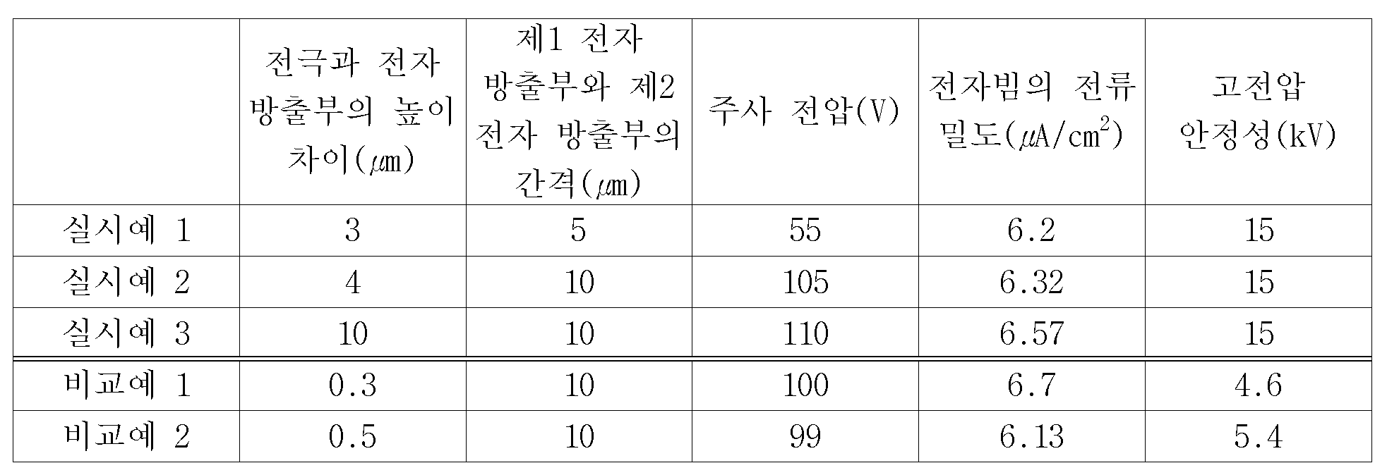
전극과 전자 방출부의 높이 차이가 1㎛보다 작은 비교예 1, 2에서는 전극에 의한 애노드 전계 차폐 효과가 낮으며, 6kV 이하의 고전압 안정성을 나타낸다. 반면, 전극과 전자 방출부의 높이 차이가 전술한 1 내지 10㎛의 조건을 만족하는 실시예 1, 2, 3에서는 애노드 전극에 15kV의 애노드 전압을 인가할 수 있으며, 아크 방전과 다이오드 에미션을 효과적으로 억제할 수 있다.In Comparative Examples 1 and 2 in which the height difference between the electrode and the electron emitting portion is smaller than 1 μm, the anode field shielding effect by the electrode is low, and high voltage stability of 6 kV or less is shown. On the other hand, in Examples 1, 2, and 3 in which the height difference between the electrode and the electron emission part satisfies the above-described conditions of 1 to 10 μm, an anode voltage of 15 kV can be applied to the anode electrode, and arc discharge and diode emission can be effectively applied. It can be suppressed.
한편, 전술한 제1 실시예와 제2 실시예에서 제1 전극(22)과 제2 전극(24)이 간격이 커질수록 전자 방출부(26, 40)에 대한 애노드 전계 차폐 효과는 감소한다. 이를 고려할 때 제1 전극(22)과 제2 전극(24)은 30 내지 200㎛의 간격을 두고 위치할 수 있다.Meanwhile, in the above-described first and second embodiments, as the distance between the
하기 표 2는 제1 전극과 제2 전극의 간격 변화에 따른 발광 장치의 고전압 안정성과 효율을 측정한 실험 결과를 나타낸다. 발광 장치의 효율은 휘도를 소비 전력으로 나눈 값을 의미한다.Table 2 below shows experimental results of measuring the high voltage stability and efficiency of the light emitting device according to the change of the distance between the first electrode and the second electrode. The efficiency of the light emitting device means a value obtained by dividing luminance by power consumption.

제1 전극과 제2 전극의 간격이 30㎛ 미만이면, 전자 방출부에 대해 애노드 전계가 과도하게 차폐되어 오히려 전자 방출부의 에미션 효율이 낮아진다. 제1 전극과 제2 전극의 간격이 20㎛인 비교예 3은 실시예 4, 5보다 낮은 20.3lm/W의 효율을 나타낸다.If the distance between the first electrode and the second electrode is less than 30 µm, the anode field is excessively shielded with respect to the electron emission portion, so that the emission efficiency of the electron emission portion is lowered. Comparative Example 3, in which the distance between the first electrode and the second electrode is 20 μm, shows an efficiency of 20.3 lm / W lower than those of Examples 4 and 5.
제1 전극과 제2 전극의 간격이 200㎛를 초과하면, 제1 전극과 제2 전극의 애노드 전계 차폐 효과가 저하된다. 따라서 발광 장치의 고전압 안정성이 낮아지고, 애노드 전극에 고전압을 인가할 수 없어 고휘도 구현이 어려워진다. 제1 전극과 제2 전극의 간격이 250㎛인 비교예 4는 실시예 4, 5보다 낮은 11kV의 고전압 안정성과 21.6lm/W의 효율을 나타낸다.When the space | interval of a 1st electrode and a 2nd electrode exceeds 200 micrometers, the anode field shielding effect of a 1st electrode and a 2nd electrode will fall. Therefore, the high voltage stability of the light emitting device is lowered, and high voltage cannot be applied to the anode electrode, making it difficult to implement high brightness. Comparative Example 4, in which the distance between the first electrode and the second electrode is 250 μm, exhibits a high voltage stability of 11 kV and an efficiency of 21.6 lm / W, which are lower than those of Examples 4 and 5.
다음으로, 도 10a 내지 도 10d를 참고하여 전술한 제2 실시예의 발광 장치 중 전자 방출 소자의 첫 번째 제조 방법에 대해 설명한다.Next, with reference to FIGS. 10A to 10D, a first manufacturing method of the electron emitting device of the above-described light emitting device of the second embodiment will be described.
도 10a를 참고하면, 제1 기판(12) 위에 금속 시트를 라미네이팅하거나 금속 페이스트를 스크린 인쇄하여 도전막을 형성하고, 도전막을 패터닝하여 제1 전극들(22)과 제2 전극들(24) 및 희생층(42)을 동시에 형성한다. 금속 시트는 알루미늄(Al) 시트일 수 있고, 금속 페이스트는 은(Ag)을 포함할 수 있다.Referring to FIG. 10A, a conductive sheet is formed by laminating a metal sheet or screen printing a metal paste on the
제1 전극들(22)과 제2 전극들(24)은 대략 3 내지 12㎛의 높이로 형성될 수 있고, 대략 30 내지 200㎛의 간격을 두고 위치할 수 있다. 희생층(42)은 대략 3 내지 20㎛의 폭으로 형성될 수 있다.The
도 10b를 참고하면, 제1 기판(12) 위에 전자 방출 물질과 감광성 물질을 포함한 페이스트상 혼합물을 스크린 인쇄한다. 전자 방출 물질은 전술한 탄소 나노튜브, 흑연, 흑연 나노파이버, 다이아몬드, 다이아몬드상 탄소, 풀러렌, 실리콘 나노와이어 및 이들의 조합으로 이루어진 군에서 선택된 물질일 수 있다. 다른 한편으로, 카바이드 유도 탄소가 전자 방출 물질로 사용될 수 있다.Referring to FIG. 10B, a paste-like mixture including an electron emission material and a photosensitive material is screen printed on the
이어서 제1 기판(12)의 후면으로부터 상기 혼합물에 자외선(화살표 참조)을 조사한다. 그러면 인쇄된 혼합물 가운데 자외선을 조사받은 부위가 선택적으로 경화된다. 그 후 현상 과정을 통해 경화되지 않은 혼합물을 제거함으로써 도 10c에 도시한 바와 같이 제1 전극(22)과 희생층(42) 사이에 제1 전자 방출부(26)를 형성하고, 제2 전극(24)과 희생층(42) 사이에 제2 전자 방출부(40)를 형성한다.Subsequently, ultraviolet rays (see arrows) are irradiated to the mixture from the rear surface of the
이때, 혼합물의 인쇄 두께와 자외선의 조사 시간 등을 제어하여 제1 전자 방출부(26)와 제2 전자 방출부(40)가 제1 전극들(22) 및 제2 전극들(24)보다 낮은 높이를 갖도록 한다. 제1 전자 방출부(26)와 제2 전자 방출부(40)는 대략 1 내지 2㎛의 두께로 형성될 수 있다.At this time, the printing thickness of the mixture, the irradiation time of ultraviolet rays, and the like are controlled so that the first
마지막으로 희생층(42)을 제거하여 도 10d에 도시한 바와 같이 제1 전자 방출부(26)와 제2 전자 방출부(40) 사이의 간격을 형성한다. 이 과정을 통해 전자 방출 소자를 완성한다.Finally, the
다음으로, 도 11a 내지 도 11e를 참고하여 전술한 제2 실시예의 발광 장치 중 전자 방출 소자의 두 번째 제조 방법에 대해 설명한다.Next, referring to FIGS. 11A to 11E, a second manufacturing method of the electron emission device among the light emitting devices of the second embodiment will be described.
도 11a를 참고하면, 제1 기판(12) 위에 금속 시트를 라미네이팅하여 도전막을 형성하고, 이 도전막을 패터닝하여 희생층(421)을 형성한다. 금속 시트는 알루미늄(Al) 시트일 수 있으며, 희생층(421)은 대략 3 내지 20㎛의 폭으로 형성될 수 있다.Referring to FIG. 11A, a conductive sheet is formed by laminating a metal sheet on the
도 11b를 참고하면, 제1 기판(12) 위에 금속 페이스트를 스크린 인쇄하여 도전막을 형성하고, 이 도전막을 패터닝하여 제1 전극들(22)과 제2 전극들(24)을 형성한다. 금속 페이스트는 은(Ag)을 포함할 수 있다. 제1 전극들과 제2 전극들은 대략 3 내지 12㎛의 높이로 형성될 수 있고, 제1 전극과 제2 전극의 간격은 대략 30 내지 200㎛일 수 있다.Referring to FIG. 11B, a conductive film is formed by screen printing a metal paste on the
도 11c를 참고하면, 제1 기판(12) 위에 전자 방출 물질과 감광성 물질을 포함한 페이스트상 혼합물을 스크린 인쇄하고, 제1 기판(12)의 후면으로부터 상기 혼합물에 자외선(화살표 참조)을 조사한다. 그러면 인쇄된 혼합물 가운데 자외선을 조사받은 부위가 선택적으로 경화된다. 그 후 현상 과정을 통해 경화되지 않은 혼합물을 제거함으로써 도 11d에 도시한 바와 같이 제1 전자 방출부(26)와 제2 전자 방출부(40)를 형성한다.Referring to FIG. 11C, a paste-like mixture containing an electron emitting material and a photosensitive material is screen printed on the
마지막으로 희생층(421)을 제거하여 도 11e에 도시한 바와 같이 제1 전자 방출부(26)와 제2 전자 방출부(40) 사이에 간격을 형성한다. 제1 전자 방출부(26)와 제2 전자 방출부(40)는 대략 1 내지 2㎛의 두께로 형성될 수 있으며, 희생층(421)의 폭에 상응하는 간격을 두고 위치한다. 이 과정을 통해 전자 방출 소자(201)를 완성한다.Finally, the
전술한 전자 방출 소자(201)에서 제1 전극들(22)과 제2 전극들(24)이 전자 방출부들(26, 40)보다 큰 높이로 형성됨에 따라, 제1 전자 방출부(26)와 제2 전자 방출부(40)는 각각 제1 전극(22) 및 제2 전극(24)에 안정적으로 접촉되고, 그 결과 전자 방출부들(26, 40)의 에미션 특성이 향상된다.In the above-described
또한, 후막 공정에 의해 형성된 제1 전극들(22) 및 제2 전극들(24)은 박막 공정에 의해 형성된 전극과 비교할 때 낮은 저항을 가진다. 따라서 발광 장치(101) 작용시 제1 전극들(22)과 제2 전극들(24)의 전압 강하를 최소화하여 휘도 균일도를 향상시킬 수 있다.In addition, the
도 12는 전술한 제1 실시예 또는 제2 실시예의 발광 장치를 광원으로 사용하는 본 발명의 일 실시예에 따른 표시 장치의 분해 사시도이고, 도 13은 도 12에 도시한 표시 패널의 부분 단면도이다.12 is an exploded perspective view of a display device according to an exemplary embodiment in which the light emitting device of the first or second embodiment is used as a light source, and FIG. 13 is a partial cross-sectional view of the display panel shown in FIG. 12. .
도 12를 참고하면, 본 실시예의 표시 장치(200)는 발광 장치(100)와, 발광 장치(100)의 전방에 위치하는 표시 패널(50)을 포함한다. 발광 장치(100)와 표시 패널(50) 사이에는 발광 장치(100)에서 출사된 빛을 고르게 확산시키는 확산판(52)이 위치할 수 있으며, 확산판(52)과 발광 장치(100)는 소정의 거리를 두고 떨어져 위치한다.Referring to FIG. 12, the
도 12에서는 제1 실시예의 발광 장치(100)가 광원으로 적용된 경우를 도시하였으나, 전술한 제2 실시예의 발광 장치(101)가 광원으로 적용될 수 있다. 표시 패널(50)은 액정 표시 패널 또는 다른 수광형 표시 패널로 이루어진다. 아래에서는 표시 패널(50)이 액정 표시 패널인 경우에 대해 설명한다.12 illustrates a case where the
도 13을 참고하면, 표시 패널(50)은 다수의 박막 트랜지스터(thin film transistor; TFT)(54)가 형성된 하부 기판(56)과, 컬러 필터층(58)이 형성된 상부 기판(60)과, 이 기판들(56, 60) 사이에 주입되는 액정층(62)을 포함한다. 상부 기판(60)의 윗면과 하부 기판(56)의 아랫면에는 각각 상부 편광판(64)과 하부 편광판(66)이 부착되어 표시 패널(50)을 통과하는 빛을 편광시킨다.Referring to FIG. 13, the
하부 기판(56)의 내면에는 부화소(sub-pixel)별로 TFT(54)에 의해 구동이 제어되는 투명한 화소 전극들(68)이 위치하고, 상부 기판(60)의 내면에는 컬러 필터층(58)과 투명한 공통 전극(70)이 위치한다. 컬러 필터층(58)은 부화소별로 하나씩 위치하는 적색 필터층과 녹색 필터층 및 청색 필터층을 포함한다.On the inner surface of the
특정 부화소의 TFT(54)가 턴 온되면, 화소 전극(68)과 공통 전극(70) 사이에 전계가 형성되고, 이 전계에 의해 액정 분자들이 배열각이 변화하며, 변화된 배열각에 따라 광 투과도가 변화한다. 표시 패널(50)은 이러한 과정을 통해 화소별 휘도와 발광색을 제어할 수 있다.When the
도 12에서 인용부호 72는 각 TFT(54)의 게이트 전극에 게이트 구동 신호를 전송하는 게이트 회로보드 어셈블리를 나타내고, 인용부호 74는 각 TFT(54)의 소스 전극에 데이터 구동 신호를 전송하는 데이터 회로보드 어셈블리를 나타낸다.In Fig. 12,
다시 도 12를 참고하면, 발광 장치(100)는 표시 패널(50)보다 적은 수의 화소들을 형성하여 발광 장치(100)의 한 화소가 2개 이상의 표시 패널(50) 화소들에 대응하도록 한다. 발광 장치(100)의 각 화소는 이에 대응하는 복수개의 표시 패널(50) 화소들 중 가장 높은 계조에 대응하여 발광할 수 있으며, 2 내지 8 비트의 계조를 표현할 수 있다.Referring back to FIG. 12, the
편의상 표시 패널(50)의 화소를 제1 화소라 하고, 발광 장치(100)의 화소를 제2 화소라 하며, 하나의 제2 화소에 대응하는 제1 화소들을 제1 화소군이라 명칭한다.For convenience, a pixel of the
발광 장치(100)의 구동 과정은, (a)표시 패널(50)을 제어하는 신호 제어부(도시하지 않음)가 제1 화소군의 제1 화소들 중 가장 높은 계조를 검출하고, (b)검출된 계조에 따라 제2 화소 발광에 필요한 계조를 산출하여 이를 디지털 데이터로 변환하고, (c)디지털 데이터를 이용하여 발광 장치(100)의 구동 신호를 생성하며, (d)생성된 구동 신호를 발광 장치(100)의 구동 전극에 인가하는 단계를 포함할 수 있다.In the driving process of the
발광 장치(100)의 구동 신호는 주사 구동 신호와 데이터 구동 신호로 이루어진다. 전술한 제1 전극들과 제2 전극들 중 어느 한 전극들(일례로 제2 전극들)이 주사 구동 신호를 인가받고, 다른 한 전극들(일례로 제1 전극들)이 데이터 구동 신호를 인가받는다.The driving signal of the
발광 장치(100)의 구동을 위한 주사 회로보드 어셈블리와 데이터 회로보드 어셈블리는 발광 장치(100)의 뒷면에 위치할 수 있다. 도 12에서 인용부호 76이 제1 전극들과 데이터 회로보드 어셈블리를 연결하는 제1 접속 부재를 나타내고, 인용부호 78이 제2 전극들과 주사 회로보드 어셈블리를 연결하는 제2 접속 부재를 나타낸다. 그리고 인용부호 80이 애노드 전극에 애노드 전압을 인가하는 제3 접속 부재를 나타낸다.The scan circuit board assembly and the data circuit board assembly for driving the
한편, 제2 실시예의 발광 장치(101)는 제1 전극들과 제2 전극들에 주사 구동 전압과 데이터 구동 전압을 교대로 반복 입력하는 구동 방식을 적용할 수 있다. 이를 위해, 제1 전극들은 제1 접속 부재(76)를 통해 주사 회로보드 어셈블리 및 데이터 회로보드 어셈블리와 연결되고, 제2 전극들 또한 제2 접속 부재(78)를 통해 주사 회로보드 어셈블리 및 데이터 회로보드 어셈블리와 연결된다.In the meantime, the
이와 같이 발광 장치(100)의 제2 화소는 대응하는 제1 화소군에 영상이 표시될 때 제1 화소군에 동기되어 소정의 계조로 발광한다. 즉, 발광 장치(100)는 표시 패널(50)이 구현하는 화면 가운데 밝은 영역에는 높은 휘도의 빛을 제공하고, 어두운 영역에는 낮은 휘도의 빛을 제공한다. 따라서 본 실시예의 표시 장치(200)는 화면의 명암비를 높이고, 보다 선명한 화질을 구현할 수 있다.As described above, when the image is displayed in the corresponding first pixel group, the second pixel of the
상기에서는 본 발명의 바람직한 실시예에 대하여 설명하였지만, 본 발명은 이에 한정되는 것이 아니고 특허청구범위와 발명의 상세한 설명 및 첨부한 도면의 범위 안에서 여러 가지로 변형하여 실시하는 것이 가능하고 이 또한 본 발명의 범위에 속하는 것은 당연하다.Although the preferred embodiments of the present invention have been described above, the present invention is not limited thereto, and various modifications and changes can be made within the scope of the claims and the detailed description of the invention and the accompanying drawings. Naturally, it belongs to the range of.
본 발명에 의한 발광 장치는 다이오드 에미션을 억제하여 화소별 휘도를 정확하게 제어할 수 있으며, 애노드 전압을 높여 발광면의 휘도를 높일 수 있다. 또한, 본 발명에 의한 발광 장치는 고전압 안정성을 높여 진공 용기 내부의 아킹 발생을 최소화하고, 아킹에 의한 내부 구조물의 손상을 억제할 수 있다. 본 발명에 의한 표시 장치는 발광 장치의 화소별 구동을 통해 화면의 명암비를 높일 수 있다.The light emitting device according to the present invention can accurately control the luminance of each pixel by suppressing diode emission, and can increase the luminance of the light emitting surface by increasing the anode voltage. In addition, the light emitting device according to the present invention can increase the high voltage stability to minimize the occurrence of arcing in the vacuum container, and can suppress the damage of the internal structure by the arcing. The display device according to the present invention can increase the contrast ratio of the screen by driving the pixel for each pixel.
Claims (19)
Priority Applications (2)
| Application Number | Priority Date | Filing Date | Title |
|---|---|---|---|
| KR1020070066582A KR100869804B1 (en) | 2007-07-03 | 2007-07-03 | Light emitting device and display device |
| US12/057,268 US20090009690A1 (en) | 2007-07-03 | 2008-03-27 | Light emission device and display device using the light emission device as light source |
Applications Claiming Priority (1)
| Application Number | Priority Date | Filing Date | Title |
|---|---|---|---|
| KR1020070066582A KR100869804B1 (en) | 2007-07-03 | 2007-07-03 | Light emitting device and display device |
Publications (1)
| Publication Number | Publication Date |
|---|---|
| KR100869804B1 true KR100869804B1 (en) | 2008-11-21 |
Family
ID=40221127
Family Applications (1)
| Application Number | Title | Priority Date | Filing Date |
|---|---|---|---|
| KR1020070066582A Expired - Fee Related KR100869804B1 (en) | 2007-07-03 | 2007-07-03 | Light emitting device and display device |
Country Status (2)
| Country | Link |
|---|---|
| US (1) | US20090009690A1 (en) |
| KR (1) | KR100869804B1 (en) |
Families Citing this family (1)
| Publication number | Priority date | Publication date | Assignee | Title |
|---|---|---|---|---|
| JP2011008946A (en) * | 2009-06-23 | 2011-01-13 | Canon Inc | Image display |
Citations (4)
| Publication number | Priority date | Publication date | Assignee | Title |
|---|---|---|---|---|
| JPH11265653A (en) | 1998-03-18 | 1999-09-28 | Ulvac Corp | Electrode, and display device having the electrode |
| KR20060012405A (en) * | 2004-08-03 | 2006-02-08 | 삼성에스디아이 주식회사 | Field emission type backlight unit and flat panel display device having same |
| KR20060061216A (en) * | 2004-12-01 | 2006-06-07 | 나노퍼시픽(주) | Field emission device driven by bipolar pulse power supply |
| KR20070011807A (en) * | 2005-07-21 | 2007-01-25 | 삼성에스디아이 주식회사 | Field emission type backlight unit and flat panel display device having same |
Family Cites Families (13)
| Publication number | Priority date | Publication date | Assignee | Title |
|---|---|---|---|---|
| US6255772B1 (en) * | 1998-02-27 | 2001-07-03 | Micron Technology, Inc. | Large-area FED apparatus and method for making same |
| JP3703415B2 (en) * | 2001-09-07 | 2005-10-05 | キヤノン株式会社 | ELECTRON EMITTING ELEMENT, ELECTRON SOURCE, IMAGE FORMING APPARATUS, AND METHOD FOR MANUFACTURING ELECTRON EMITTING ELEMENT AND ELECTRON SOURCE |
| JPWO2003073458A1 (en) * | 2002-02-26 | 2005-06-23 | 日本碍子株式会社 | Electron emitting device, driving method of electron emitting device, display, and driving method of display |
| US7187114B2 (en) * | 2002-11-29 | 2007-03-06 | Ngk Insulators, Ltd. | Electron emitter comprising emitter section made of dielectric material |
| KR100943192B1 (en) * | 2003-11-25 | 2010-02-19 | 삼성에스디아이 주식회사 | Field emission display device and manufacturing method thereof |
| US20050231978A1 (en) * | 2004-03-23 | 2005-10-20 | Kvenvold Anthony M | High efficiency low power LED backlighting system for liquid crystal display |
| KR101096720B1 (en) * | 2004-05-28 | 2011-12-22 | 엘지디스플레이 주식회사 | Apparatus and method for driving liquid crystal display device |
| KR100634542B1 (en) * | 2005-04-15 | 2006-10-13 | 삼성에스디아이 주식회사 | Field emission type backlight unit, its driving method and manufacturing method of lower panel |
| KR20070010660A (en) * | 2005-07-19 | 2007-01-24 | 삼성에스디아이 주식회사 | Electron emitting device and flat panel display device having the same |
| KR20070011806A (en) * | 2005-07-21 | 2007-01-25 | 삼성에스디아이 주식회사 | Field emission type backlight unit and flat panel display device having same |
| KR20070011803A (en) * | 2005-07-21 | 2007-01-25 | 삼성에스디아이 주식회사 | Electron emitting device and flat panel display device having the same |
| US8228272B2 (en) * | 2006-12-22 | 2012-07-24 | Hong Kong Applied Science And Technlogy Research Institute Company Limited | Backlight device and liquid crystal display incorporating the backlight device |
| KR100879473B1 (en) * | 2007-09-17 | 2009-01-20 | 삼성에스디아이 주식회사 | Electron emitting device, light emitting device having same and method of manufacturing electron emitting device |
-
2007
- 2007-07-03 KR KR1020070066582A patent/KR100869804B1/en not_active Expired - Fee Related
-
2008
- 2008-03-27 US US12/057,268 patent/US20090009690A1/en not_active Abandoned
Patent Citations (4)
| Publication number | Priority date | Publication date | Assignee | Title |
|---|---|---|---|---|
| JPH11265653A (en) | 1998-03-18 | 1999-09-28 | Ulvac Corp | Electrode, and display device having the electrode |
| KR20060012405A (en) * | 2004-08-03 | 2006-02-08 | 삼성에스디아이 주식회사 | Field emission type backlight unit and flat panel display device having same |
| KR20060061216A (en) * | 2004-12-01 | 2006-06-07 | 나노퍼시픽(주) | Field emission device driven by bipolar pulse power supply |
| KR20070011807A (en) * | 2005-07-21 | 2007-01-25 | 삼성에스디아이 주식회사 | Field emission type backlight unit and flat panel display device having same |
Also Published As
| Publication number | Publication date |
|---|---|
| US20090009690A1 (en) | 2009-01-08 |
Similar Documents
| Publication | Publication Date | Title |
|---|---|---|
| US7629735B2 (en) | Light emission device and display device | |
| KR20090023903A (en) | Light emitting device and display device using the light emitting device as a light source | |
| CN101483130B (en) | Light emission device and display device using the same as light source | |
| US7737620B2 (en) | Light emission device, method of manufacturing electron emission unit for the light emission device, and display device having the light emission device | |
| JP2007311355A (en) | Light emitting device and display device | |
| JP2010010120A (en) | Light-emitting device and display device using it as light source | |
| KR20090006352A (en) | Light emitting device and display device using the light emitting device as a light source | |
| KR100869804B1 (en) | Light emitting device and display device | |
| KR100863959B1 (en) | Light emitting device and display device having same | |
| KR100889527B1 (en) | Light emitting device and display device using the light emitting device as a light source | |
| KR20100083555A (en) | Light emission device and display device using the same | |
| KR100778517B1 (en) | Light emitting device and display device | |
| JP4731531B2 (en) | Light emitting device and display device using this light emitting device as light source | |
| EP1890320A2 (en) | Light emission device and display device using the light emission device as light source | |
| CN100578723C (en) | Light emitting device, manufacturing method of electron emission unit, and display device | |
| KR20090009502A (en) | Light emitting device and display device having the light emitting device | |
| KR100814846B1 (en) | Light-emitting device and liquid crystal display device using this light-emitting device as backlight unit | |
| KR20080043536A (en) | Light emitting device and display device | |
| US20100176712A1 (en) | Light emission device and display device having the same | |
| KR20100082048A (en) | Light emission device and display device using the same | |
| KR20080075661A (en) | Light emitting device, manufacturing method thereof and display device using same | |
| US20100172125A1 (en) | Light emission device and display device using the same | |
| KR20080105279A (en) | Light emitting device and display device using the light emitting device as a light source | |
| KR20080108727A (en) | Light emitting device and display device using the light emitting device as a light source | |
| KR20080102781A (en) | Light emitting device and display device |
Legal Events
| Date | Code | Title | Description |
|---|---|---|---|
| A201 | Request for examination | ||
| PA0109 | Patent application |
St.27 status event code: A-0-1-A10-A12-nap-PA0109 |
|
| PA0201 | Request for examination |
St.27 status event code: A-1-2-D10-D11-exm-PA0201 |
|
| D13-X000 | Search requested |
St.27 status event code: A-1-2-D10-D13-srh-X000 |
|
| D14-X000 | Search report completed |
St.27 status event code: A-1-2-D10-D14-srh-X000 |
|
| E902 | Notification of reason for refusal | ||
| PE0902 | Notice of grounds for rejection |
St.27 status event code: A-1-2-D10-D21-exm-PE0902 |
|
| E13-X000 | Pre-grant limitation requested |
St.27 status event code: A-2-3-E10-E13-lim-X000 |
|
| P11-X000 | Amendment of application requested |
St.27 status event code: A-2-2-P10-P11-nap-X000 |
|
| P13-X000 | Application amended |
St.27 status event code: A-2-2-P10-P13-nap-X000 |
|
| E701 | Decision to grant or registration of patent right | ||
| PE0701 | Decision of registration |
St.27 status event code: A-1-2-D10-D22-exm-PE0701 |
|
| GRNT | Written decision to grant | ||
| PR0701 | Registration of establishment |
St.27 status event code: A-2-4-F10-F11-exm-PR0701 |
|
| PR1002 | Payment of registration fee |
St.27 status event code: A-2-2-U10-U11-oth-PR1002 Fee payment year number: 1 |
|
| PG1601 | Publication of registration |
St.27 status event code: A-4-4-Q10-Q13-nap-PG1601 |
|
| R18-X000 | Changes to party contact information recorded |
St.27 status event code: A-5-5-R10-R18-oth-X000 |
|
| R18-X000 | Changes to party contact information recorded |
St.27 status event code: A-5-5-R10-R18-oth-X000 |
|
| FPAY | Annual fee payment |
Payment date: 20111024 Year of fee payment: 4 |
|
| PR1001 | Payment of annual fee |
St.27 status event code: A-4-4-U10-U11-oth-PR1001 Fee payment year number: 4 |
|
| LAPS | Lapse due to unpaid annual fee | ||
| PC1903 | Unpaid annual fee |
St.27 status event code: A-4-4-U10-U13-oth-PC1903 Not in force date: 20121115 Payment event data comment text: Termination Category : DEFAULT_OF_REGISTRATION_FEE |
|
| PC1903 | Unpaid annual fee |
St.27 status event code: N-4-6-H10-H13-oth-PC1903 Ip right cessation event data comment text: Termination Category : DEFAULT_OF_REGISTRATION_FEE Not in force date: 20121115 |
|
| R18-X000 | Changes to party contact information recorded |
St.27 status event code: A-5-5-R10-R18-oth-X000 |
|
| P22-X000 | Classification modified |
St.27 status event code: A-4-4-P10-P22-nap-X000 |
|
| R18-X000 | Changes to party contact information recorded |
St.27 status event code: A-5-5-R10-R18-oth-X000 |