KR100855965B1 - Bidirectional JRAM having a subcell array and data writing method using the same - Google Patents
Bidirectional JRAM having a subcell array and data writing method using the same Download PDFInfo
- Publication number
- KR100855965B1 KR100855965B1 KR1020070001180A KR20070001180A KR100855965B1 KR 100855965 B1 KR100855965 B1 KR 100855965B1 KR 1020070001180 A KR1020070001180 A KR 1020070001180A KR 20070001180 A KR20070001180 A KR 20070001180A KR 100855965 B1 KR100855965 B1 KR 100855965B1
- Authority
- KR
- South Korea
- Prior art keywords
- input
- memory device
- voltage
- cell
- output lines
- Prior art date
- Legal status (The legal status is an assumption and is not a legal conclusion. Google has not performed a legal analysis and makes no representation as to the accuracy of the status listed.)
- Active
Links
Images


Classifications
-
- G—PHYSICS
- G11—INFORMATION STORAGE
- G11C—STATIC STORES
- G11C13/00—Digital stores characterised by the use of storage elements not covered by groups G11C11/00, G11C23/00, or G11C25/00
-
- G—PHYSICS
- G11—INFORMATION STORAGE
- G11C—STATIC STORES
- G11C13/00—Digital stores characterised by the use of storage elements not covered by groups G11C11/00, G11C23/00, or G11C25/00
- G11C13/0002—Digital stores characterised by the use of storage elements not covered by groups G11C11/00, G11C23/00, or G11C25/00 using resistive RAM [RRAM] elements
- G11C13/0021—Auxiliary circuits
- G11C13/0023—Address circuits or decoders
-
- G—PHYSICS
- G11—INFORMATION STORAGE
- G11C—STATIC STORES
- G11C13/00—Digital stores characterised by the use of storage elements not covered by groups G11C11/00, G11C23/00, or G11C25/00
- G11C13/0002—Digital stores characterised by the use of storage elements not covered by groups G11C11/00, G11C23/00, or G11C25/00 using resistive RAM [RRAM] elements
- G11C13/0021—Auxiliary circuits
- G11C13/0069—Writing or programming circuits or methods
-
- G—PHYSICS
- G11—INFORMATION STORAGE
- G11C—STATIC STORES
- G11C16/00—Erasable programmable read-only memories
- G11C16/02—Erasable programmable read-only memories electrically programmable
- G11C16/06—Auxiliary circuits, e.g. for writing into memory
- G11C16/10—Programming or data input circuits
-
- G—PHYSICS
- G11—INFORMATION STORAGE
- G11C—STATIC STORES
- G11C13/00—Digital stores characterised by the use of storage elements not covered by groups G11C11/00, G11C23/00, or G11C25/00
- G11C13/0002—Digital stores characterised by the use of storage elements not covered by groups G11C11/00, G11C23/00, or G11C25/00 using resistive RAM [RRAM] elements
- G11C13/0021—Auxiliary circuits
- G11C13/0069—Writing or programming circuits or methods
- G11C2013/0088—Write with the simultaneous writing of a plurality of cells
-
- G—PHYSICS
- G11—INFORMATION STORAGE
- G11C—STATIC STORES
- G11C13/00—Digital stores characterised by the use of storage elements not covered by groups G11C11/00, G11C23/00, or G11C25/00
- G11C13/0002—Digital stores characterised by the use of storage elements not covered by groups G11C11/00, G11C23/00, or G11C25/00 using resistive RAM [RRAM] elements
- G11C13/0021—Auxiliary circuits
- G11C13/0069—Writing or programming circuits or methods
- G11C2013/009—Write using potential difference applied between cell electrodes
Landscapes
- Semiconductor Memories (AREA)
- Static Random-Access Memory (AREA)
Abstract
서브 셀 어레이를 구비하는 양방향성 R R A M 및 이를 이용하는 데이터 기입 방법이 개시된다. 본 발명의 실시예에 따른 셀 양단 전압의 극성에 따라 데이터 값이 결정되는 비휘발성 메모리 장치는 적어도 하나 이상의 입출력 라인을 포함하는 소정수의 서브 셀 어레이들을 포함하는 메모리 셀 어레이를 구비한다. 상기 서브 셀 어레이들 각각 독립된 X-디코더 및 드라이버를 구비한다. 본 발명에 따른 양방향성 R R A M 및 이를 이용하는 데이터 기입 방법은 독립된 X-디코더 및 드라이버를 구비하는 서브 셀 어레이들을 구비함으로써 비록 데이터 값이 다른 경우에도 동시에 기입 동작을 수행할 수 있는 장점이 있다.Disclosed are a bidirectional R R A M having a sub cell array and a data writing method using the same. A nonvolatile memory device in which a data value is determined according to a polarity of a voltage across a cell according to an exemplary embodiment of the present invention includes a memory cell array including a predetermined number of subcell arrays including at least one input / output line. Each of the subcell arrays has an independent X-decoder and driver. The bidirectional R R A M and the data writing method using the same according to the present invention have the advantage of being able to simultaneously perform writing operations even if the data values are different by having sub-cell arrays having independent X-decoder and drivers.
양방향성 RRAM, 서브 셀 어레이, 비휘발성 메모리 Bidirectional RRAM, Subcell Array, Nonvolatile Memory
Description
본 발명의 상세한 설명에서 인용되는 도면을 보다 충분히 이해하기 위하여 각 도면의 간단한 설명이 제공된다. BRIEF DESCRIPTION OF THE DRAWINGS In order to better understand the drawings cited in the detailed description of the invention, a brief description of each drawing is provided.
도 1는 양방향성 RRAM의 셀 구조를 개략적으로 나타내는 도면이다.1 is a diagram schematically illustrating a cell structure of a bidirectional RRAM.
도 2는 도 1의 셀 특성을 나타내는 그래프이다.FIG. 2 is a graph showing cell characteristics of FIG. 1.
도 3의 (a) 및 (b)는 도 1의 셀에 데이터를 기입하는 동작을 개략적으로 나타내는 도면이다.3A and 3B are diagrams schematically showing an operation of writing data into the cell of FIG.
도 4는 도 3의 (a)의 기입 동작을 보다 자세하게 나타내는 도면이다.FIG. 4 is a diagram showing the writing operation of FIG. 3A in more detail.
도 5는 본 발명의 실시예에 따른 양방향성 RRAM을 개략적으로 나타내는 블럭도이다.5 is a block diagram schematically illustrating a bidirectional RRAM according to an embodiment of the present invention.
도 6은 본 발명의 다른 실시예에 따른 양방향성 RRAM을 개략적으로 나타내는 블럭도이다.6 is a block diagram schematically illustrating a bidirectional RRAM according to another embodiment of the present invention.
도 7은 도 6의 서브 셀 어레이를 보다 자세히 나타내는 도면이다.FIG. 7 illustrates the subcell array of FIG. 6 in more detail.
본 발명은 비휘발성 메모리 장치에 관한 것으로서, 특히 독립된 X-디코더 및 드라이버를 갖는 서브 셀 어레이들을 구비하여 데이터 값이 다른 경우에도 동시에 기입 동작을 수행할 수 있는 양방향성 R R A M 및 이를 이용하는 데이터 기입 방법에 관한 것이다. BACKGROUND OF THE
차세대 메모리 장치는 DRAM(Dynamic Random Access Memory)의 고집적성, FLASH 메모리의 비휘발성, SRAM(Static RAM)의 고속성 등을 갖출 것이 요구되고 있다. 현재 PRAM(Phase change RAM), NFGM(Nano Floating Gate Memory), PoRAM(Polymer RAM), MRAM(Magnetic RAM), FeRAM(Ferroelectric RAM), RRAM(Resistive RAM) 등이 상기와 같은 요구에 부응하는 차세대 메모리 장치로 거론되고 있다.Next-generation memory devices are required to have high integration of DRAM (Dynamic Random Access Memory), nonvolatile FLASH memory, high speed of Static RAM (SRAM), and the like. Next-generation memory that Pha (Phase change RAM), Nano Floating Gate Memory (NFGM), Polymer RAM (PoRAM), Magnetic RAM (MRAM), Ferroelectric RAM (FeRAM), and Resistive RAM (RRAM) meet these needs. It is mentioned as a device.
도 1는 양방향성 RRAM의 셀 구조를 개략적으로 나타내는 도면이다.1 is a diagram schematically illustrating a cell structure of a bidirectional RRAM.
도 1을 참조하면, 양방향성 RRAM은 나노믹(non-ohmic) 물질 및 저항 가변 소자를 구비한다. RRAM은 저항 가변 소자의 저항값 변화를 이용하여 데이터를 기입한다. 저항 가변 소자는 제 1 전극과 제 2 전극사이에 저항 가변체(Resistance variable substance)를 구비한다. Referring to FIG. 1, a bidirectional RRAM includes a non-ohmic material and a resistive variable element. The RRAM writes data using the change in the resistance value of the resistance variable element. The resistance variable element includes a resistance variable substance between the first electrode and the second electrode.
저항 가변체는 인가되는 전압 또는 전류에 따라서 저항값이 변한다. 단방향성(uni-directional) RRAM의 경우, 인가되는 전압 또는 전류의 크기에 따라서 저항값이 변한다. 반면, 양방향성(bi-directional) RRAM의 경우, 인가되는 전압 또는 전류의 크기 및 방향에 따라서 저항값이 변한다. The resistance variable changes in resistance value depending on the voltage or current applied. In the case of uni-directional RRAM, the resistance changes depending on the magnitude of the voltage or current applied. On the other hand, in the case of bi-directional RRAM, the resistance value changes according to the magnitude and direction of the applied voltage or current.
도 1의 양방향성 RRAM은 나노믹 물질을 구비함으로써 상기와 같은 양방향성을 실현한다. 나노믹 물질은 소정의 전압 범위(-3V ~ 3V) 내에서는 고저항 상태를 갖는다. 따라서, 저항 가변 소자에 전류가 인가되지 아니한다. 반면, 상기 소정의 전압 범위 이외(-3V 이하 또는 3V 이상)에서는 저저항 상태를 갖는다. 따라서, 저항 가변 소자에 전류를 인가한다. 나노믹 물질 및 저항 가변 소자를 구비하는 양방향성 RRAM에 대해서는 미국등록특허 제 6,909,632 호에 보다 자세히 설명된다.The bidirectional RRAM of FIG. 1 realizes such bidirectionality by providing a nanomic material. Nanomic materials have a high resistance state within a predetermined voltage range (-3V to 3V). Therefore, no current is applied to the resistance variable element. On the other hand, it has a low resistance state outside the predetermined voltage range (below -3V or above 3V). Therefore, a current is applied to the resistance variable element. Bidirectional RRAMs with nanomic materials and resistive variable elements are described in more detail in US Pat. No. 6,909,632.
도 2는 도 1의 셀 특성을 나타내는 그래프이다.FIG. 2 is a graph showing cell characteristics of FIG. 1.
도 1 및 도 2를 참조하면, 저항 가변체에 6V의 기입 전압(VW)이 인가되면, 대응되는 셀은 제 1 저항값을 갖는다. 반면, 저항 가변체에 -6V의 기입 전압(-VW)이 인가되면, 대응되는 셀은 제 2 저항값을 갖는다. 1 and 2, when the write voltage V W of 6 V is applied to the resistance variable, the corresponding cell has a first resistance value. On the other hand, when a write voltage (-V W ) of -6V is applied to the resistance variable, the corresponding cell has a second resistance value.
양방향성 RRAM에서 데이터 "1"은 셀이 제 1 저항값을 갖는 경우로, 데이터 "0"은 셀이 제 2 저항값을 갖는 경우로 설정될 수 있다. 즉, 양방향성 RRAM에서, 데이터 "1" 및 "0"은 서로 셀 양단 전압의 크기는 동일하나 극성이 반대인 기입 전압을 사용하여 기입할 수 있다. In the bidirectional RRAM, data "1" may be set when the cell has a first resistance value, and data "0" may be set when the cell has a second resistance value. That is, in the bidirectional RRAM, data "1" and "0" can be written using write voltages having the same magnitude across the cell but opposite polarities.
도 3의 (a) 및 (b)는 도 1의 셀에 데이터를 기입하는 동작을 개략적으로 나타내는 도면이다.3A and 3B are diagrams schematically showing an operation of writing data into the cell of FIG.
도 3의 (a)를 참조하면, 워드 라인(WL)에 3V를 인가하고 비트 라인(BL)에 -3V를 인가함으로써 데이터 "0"이 셀(동그라미 표시)에 기입된다. 반면, 워드 라인(WL)에 -3V를 인가하고 비트 라인(BL)에 3V를 인가함으로써 데이터 "1"이 셀에 기입된다. 이때, 비선택된 워드 라인(WL`) 및 비트 라인(BL`)에는 0V가 인가된다. Referring to FIG. 3A, data "0" is written into a cell (circle display) by applying 3V to the word line WL and -3V to the bit line BL. On the other hand, data "1" is written to the cell by applying -3V to the word line WL and 3V to the bit line BL. At this time, 0 V is applied to the unselected word line WL` and the bit line BL`.
도 3의 (b)를 참조하면, 워드 라인(WL)에 6V를 인가하고 비트 라인(BL)에 0V를 인가하며 비선택된 워드 라인(WL`) 및 비트 라인(BL`)에 3V를 인가함으로써, 데이터 "0"이 셀에 기입된다. 반면, 워드 라인(WL)에 0V를 인가하고 비트 라인(BL)에 -6V를 인가하며 비선택된 워드 라인(WL`) 및 비트 라인(BL`)에 -3V를 인가함으로써. 데이터 "1"이 셀에 기입된다. Referring to FIG. 3B, by applying 6V to the word line WL, applying 0V to the bit line BL, and applying 3V to the unselected word lines WL` and bit line BL`. , Data "0" is written into the cell. On the other hand, by applying 0V to the word line WL, -6V to the bit line BL, and -3V to the unselected word line WL` and bit line BL`. Data "1" is written to the cell.
다만, 도 3의 (b)와 같이 기입 전압(VW = 6V, -VW = -6V)을 워드 라인 또는 비트 라인에 인가하여 데이터를 기입하는 경우는 데이터 값에 따라 비선택된 워드 라인 및 비트 라인의 전압이 달라지는 바, 도 3의 (a)의 기입 전압의 1/2 전압(1/2VW = 3V, -1/2VW = -3V)을 워드 라인 또는 비트 라인에 인가하여 데이터를 기입하는 것이 보다 효율적이라 할 수 있다. 이하에서는, 설명의 편의를 위해 도 3의 (a)와 같이 동작하는 양방향성 RRAM에 대하여 기술한다. However, in the case of writing data by applying the write voltage (V W = 6V, -V W = -6V) to the word line or the bit line as shown in FIG. 3 (b), the unselected word line and bit according to the data value Since the voltage of the line varies, 1/2 data (1 / 2V W = 3V, -1 / 2V W = -3V) of the write voltage of FIG. 3A is applied to the word line or the bit line to write data. It is more efficient to do. Hereinafter, for convenience of description, a bidirectional RRAM operating as shown in FIG. 3A will be described.
도 4는 도 3의 (a)의 기입 동작을 보다 자세하게 나타내는 도면이다.FIG. 4 is a diagram showing the writing operation of FIG. 3A in more detail.
도 4를 참조하면, 입출력 라인들(IO0 ~ IO15)이 워드 라인(WLi, WLj)을 공유한다. 즉, 메모리 셀 어레이의 모든 입출력 라인들(IO0 ~ IO15)이 하나의 X-디코더 및 드라이버를 공유한다.Referring to FIG. 4, the input / output lines IO0 to IO15 share the word lines WLi and WLj. That is, all input / output lines IO0 to IO15 of the memory cell array share one X-decoder and driver.
그런데, 하나의 워드 라인(WLi)에는 도 3의 (a)의 극성이 다른 바이어스 전압(1/2VW = 3V, -1/2VW = -3V)을 동시에 인가할 수 없다. 따라서, 워드 라인을 공유하는 입출력 라인들 중 기입하고자 하는 데이터 값이 다른 입출력 라인이 하나라도 존재한다면, 모든 입출력 라인들에 대해 데이터를 동시에 기입할 수 없는 문제가 발생한다. However, a bias voltage (1 / 2V W = 3V, -1 / 2V W = -3V) having different polarities in FIG. 3A cannot be simultaneously applied to one word line WLi. Therefore, when one input / output line having a different data value to be written among the input / output lines sharing a word line exists, a problem occurs in that data cannot be simultaneously written to all the input / output lines.
본 발명이 이루고자하는 기술적 과제는 기입하고자 하는 데이터 값이 다른 경우에도 기입 동작을 수행할 수 있는 양방향성 RRAM을 제공하는데 있다. An object of the present invention is to provide a bidirectional RRAM capable of performing a write operation even when data values to be written are different.
본 발명이 이루고자하는 다른 기술적 과제는 기입하고자 하는 데이터 값이 다른 경우에도 기입 동작을 수행할 수 있는 양방향성 RRAM에서의 데이터 기입 방법을 제공하는데 있다. Another object of the present invention is to provide a data writing method in a bidirectional RRAM capable of performing a write operation even when data values to be written are different.
상기 기술적 과제를 달성하기 위한 본 발명의 실시예에 따른 셀 양단 전압의 극성에 따라 데이터 값이 결정되는 비휘발성 메모리 장치는 적어도 하나 이상의 입출력 라인을 포함하는 소정수의 서브 셀 어레이들을 포함하는 메모리 셀 어레이를 구비한다. 상기 서브 셀 어레이들 각각 독립된 X-디코더 및 드라이버를 구비한다. According to another aspect of the present invention, a nonvolatile memory device in which a data value is determined according to a polarity of a voltage across a cell includes a memory cell including a predetermined number of subcell arrays including at least one input / output line. With an array. Each of the subcell arrays has an independent X-decoder and driver.
상기 X-디코더 및 드라이버는 대응되는 워드 라인을 활성화하고, 상기 활성화된 워드 라인에 데이터 값에 따른 바이어스 전압을 인가한다. 상기 서브 셀 어레이들은 각각 포함되는 워드 라인들을 공유하는 복수개의 입출력 라인들을 구비할 수 있다. 바람직하게는 상기 서브 셀 어레이들은 각각 4 개의 입출력 라인들을 구비한다. The X-decoder and the driver activate a corresponding word line and apply a bias voltage according to a data value to the activated word line. The subcell arrays may include a plurality of input / output lines each sharing word lines included therein. Preferably, the sub cell arrays each have four input / output lines.
상기 서브 셀 어레이들은 각각 상기 입출력 라인들에 대응되는 Y-디코더들 및 기입 드라이버들을 구비한다. 상기 비휘발성 메모리 장치는 포함되는 서브 셀 어레이를 달리하는 입출력 라인들을 동시에 활성화/하고, 상기 데이터 값에 따른 바이어스 전압을 상기 활성화된 입출력 라인에 인가한다. 상기 비휘발성 메모리 장치는 포함되는 서브 셀 어레이를 같이하는 입출력 라인들을 순차적으로 활성화한다. The subcell arrays each include Y-decoders and write drivers corresponding to the input / output lines. The nonvolatile memory device simultaneously activates / outputs input / output lines different from an included subcell array, and applies a bias voltage according to the data value to the activated input / output line. The nonvolatile memory device sequentially activates input / output lines that share the included subcell array.
바람직하게는 상기 서브 셀 어레이들은 각각 하나의 입출력 라인을 구비한다. 상기 서브 셀 어레이들은 각각 상기 입출력 라인에 대응되는 Y-디코더 및 드라이버를 구비한다.Preferably, the sub cell arrays each have one input / output line. The subcell arrays each include a Y-decoder and a driver corresponding to the input / output line.
상기 바이어스 전압은 상기 데이터의 기입 전압에 상응한다. 상기 기입 전압은 상기 데이터 값에 따라 크기는 동일하나 극성이 반대이다.The bias voltage corresponds to the write voltage of the data. The write voltage is equal in magnitude but opposite in polarity according to the data value.
상기 비휘발성 메모리 장치는 양방향성 RRAM(Resistive Random Access Memory)이다. 상기 양방향성 RRAM은 나노믹(non-ohmic) 디바이스 및 저항 가변 물질을 구비한다. 나노믹 디바이스는 상기 셀 양단 전압이 일정 전압 범위 내인 경우에는 고저항 상태 물질로서 동작하고 상기 전압 범위 이외에서는 저저항 상태로 동작한다. 저항 가변 물질은 상기 나노믹 디바이스가 저저항 상태인 경우, 상기 셀 양단 전압의 극성에 따라 다른 저항값을 갖는다.The nonvolatile memory device is a bidirectional resistive random access memory (RRAM). The bidirectional RRAM includes a non-ohmic device and a resistive variable material. The nanomic device operates as a high resistance state material when the voltage across the cell is within a predetermined voltage range and operates in a low resistance state outside the voltage range. The resistance variable material has a different resistance value depending on the polarity of the voltage across the cell when the nanomic device is in the low resistance state.
상기 다른 기술적 과제를 달성하기 위한 본 발명의 실시예에 따른 셀 양단 전압의 극성에 따라 데이터 값이 결정되는 비휘발성 메모리 장치에서의 데이터 기입 방법은, 서브 셀 어레이를 달리하는 입출력 라인들을 동시에 활성화하여, 상기 데이터 값에 따른 바이어스 전압을 상기 활성화된 입출력 라인들에 인가하는 단계 및 상기 서브 셀 어레이를 달리하는 워드 라인들을 상기 데이터 값에 따른 바이어 스 전압을 상기 활성화된 워드 라인들에 인가하는 단계를 구비한다.According to another aspect of the present invention, a data writing method of a nonvolatile memory device in which a data value is determined according to a polarity of a voltage across a cell may be performed by simultaneously activating input / output lines of different subcell arrays. Applying a bias voltage according to the data value to the activated input / output lines; and applying a bias voltage according to the data value to the activated word lines; Equipped.
본 발명과 본 발명의 동작상의 이점 및 본 발명의 실시에 의하여 달성되는 목적을 충분히 이해하기 위해서는 본 발명의 바람직한 실시예를 예시하는 첨부 도면 및 도면에 기재된 내용을 참조하여야 한다. DETAILED DESCRIPTION In order to fully understand the present invention, the operational advantages of the present invention, and the objects achieved by the practice of the present invention, reference should be made to the accompanying drawings which illustrate preferred embodiments of the present invention and the contents described in the drawings.
이하, 첨부한 도면을 참조하여 본 발명이 바람직한 실시예를 설명함으로써, 본 발명을 상세히 설명한다. 각 도면에 제시된 동일한 참조부호는 동일한 부재를 나타낸다.Hereinafter, exemplary embodiments of the present invention will be described in detail with reference to the accompanying drawings. Like reference numerals in the drawings denote like elements.
도 5는 본 발명의 실시예에 따른 양방향성 RRAM을 개략적으로 나타내는 블럭도이다.5 is a block diagram schematically illustrating a bidirectional RRAM according to an embodiment of the present invention.
도 5를 참조하면, 도 5의 서브 셀 어레이들(SCA0 ~ SCA15)은 각각 대응되는 1 개의 입출력 라인(IO0 ~ IO15)을 구비한다. 도 5의 서브 셀 어레이들(SCA0 ~ SCA15)은 또한, 각각 독립된 X-디코더/드라이버(X DEC & DRV0 ~ X DEC & DRV15) 및 Y-디코더/드라이버(Y DEC & WDRV00 ~ Y DEC & WDRV015)를 구비한다. 예를 들어, 제 1 서브 셀 어레이(SCA0)는 입출력 라인(IO0), X-디코더/드라이버(X DEC & DRV0) 및 Y-디코더/드라이버(Y DEC & WDRV00)를 구비한다. Referring to FIG. 5, each of the subcell arrays SCA0 to SCA15 of FIG. 5 includes one input / output line IO0 to IO15 corresponding to each other. Sub-cell arrays SCA0 to SCA15 of FIG. 5 are also independent X-decoder / drivers (X DEC & DRV0 to X DEC & DRV15) and Y-decoder / drivers (Y DEC & WDRV00 to Y DEC & WDRV015), respectively. It is provided. For example, the first sub-cell array SCA0 includes an input / output line IO0, an X-decoder / driver X XC and DRV0, and a Y-decoder / driver YC and WDRV00.
이렇게 도 5의 양방향성 RRAM은 서브 셀 어레이들(SCA0 ~ SCA15)이 각각의 입출력 라인에 대응되는 X-디코더/드라이버 및 Y-디코더/드라이버를 따로 구비함으로써, 동시에 모든 입출력 라인들에 대한 기입 동작을 수행할 수 있다. 다만, 전류 펌핑(pumping) 제한 등의 문제로 16개의 입출력 라인(IO)에 대하여 X4로 4번에 걸쳐 기입 동작을 수행하는 스킴을 채택하는 시스템에서는 다음의 도 6과 같이 서브 셀 어레이를 구성할 수 있다. As described above, the bidirectional RRAM of FIG. 5 provides the X-decoder / driver and the Y-decoder / driver corresponding to each input / output line of the subcell arrays SCA0 to SCA15 separately, thereby simultaneously performing a write operation on all the input / output lines. Can be done. However, in a system adopting a scheme of performing write operations four times with X4 on 16 input / output lines IO due to problems such as current pumping limitation, a subcell array may be configured as shown in FIG. Can be.
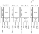
도 6는 본 발명의 다른 실시예에 따른 양방향성 RRAM을 개략적으로 나타내는 블럭도이다.6 is a block diagram schematically illustrating a bidirectional RRAM according to another embodiment of the present invention.
도 7은 도 6의 서브 셀 어레이를 보다 자세히 나타내는 도면이다. FIG. 7 illustrates the subcell array of FIG. 6 in more detail.
도 6 및 도 7을 참조하면, 본 발명의 실시예에 따른 양방향성 RRAM(100)의 셀들은 나노믹(non-ohmic) 디바이스 및 저항 가변 물질을 구비한다. 나노믹 디바이스는 상기 셀 양단 전압이 일정 전압 범위 내인 경우에는 고저항 상태 물질로서 동작하고 상기 전압 범위 이외에서는 저저항 상태로 동작한다. 저항 가변 물질은 상기 나노믹 디바이스가 저저항 상태인 경우, 상기 셀 양단 전압의 극성에 따라 다른 저항값을 갖는다. 이에 대한 보다 자세한 설명은 전술되어 있으므로 생략한다. 6 and 7, the cells of the
본 발명의 실시예에 따른 양방향성 RRAM(100)은 소정수의 서브 셀 어레이들(SCA0 ~ SCA3)을 포함하는 메모리 셀 어레이를 구비한다. 서브 셀 어레이들(SCA0 ~ SCA3)은 각각의 독립된 X-디코더 및 드라이버(X DEC & DRV0 ~ X DEC & DRV3)를 구비한다. The
도 5의 서브 셀 어레이들(SCA0 ~ SCA3)은 각각 4 개의 입출력 라인들을 포함한다. 서브 셀 어레이들(SCA0 ~ SCA3)은 또한 각각 상기 입출력 라인들에 대응되는 Y-디코더들 및 드라이버들을 구비한다. Each of the sub cell arrays SCA0 to SCA3 of FIG. 5 includes four input / output lines. The subcell arrays SCA0 to SCA3 also have Y-decoders and drivers corresponding to the input / output lines, respectively.
예를 들어, 도 7의 제 1 서브 셀 어레이(SCA0)는 독립된 X-디코더 및 드라이버(X DEC & DRV0), 4개의 입출력 라인들(IO0, IO4, IO8, IO12) 및 각각의 입출력 라인들을 담당하는 Y-디코더들 및 드라이버들(Y DEC & WDRV00, Y DEC & WDRV04, Y DEC & WDRV08,Y DEC & WDRV012)을 구비한다. For example, the first subcell array SCA0 of FIG. 7 is responsible for an independent X-decoder and driver X DEC & DRV0, four input / output lines IO0, IO4, IO8, and IO12, and respective input / output lines. Y-decoders and drivers (Y DEC & WDRV00, Y DEC & WDRV04, Y DEC & WDRV08, Y DEC & WDRV012).
도 6의 양방향성 RRAM(100)은 포함되는 서브 셀 어레이를 달리하는 입출력 라인들을 동시에 활성화하고, 상기 활성화된 입출력 라인들에 각각 대응되는 데이터 값에 따른 바이어스 전압을 인가한다. 또한, X-디코더 및 드라이버는 워드 라인을 활성화하고, 활성화된 워드 라인에 데이터 값에 따른 바이어스 전압을 인가한다.The
이때, 바이어스 전압은 상기 데이터의 기입 전압에 상응한다. 도 3의 (a)의 RRAM은 워드 라인 및 비트 라인에 인가되는 바이어스 전압이 기입 전압의 1/2 또는 -1/2 값으로 설정되고, 도 3의 (b)의 RRAM은 워드 라인 및 비트 라인에 인가되는 바이어스 전압이 기입 전압 또는 "0"으로 설정된다. In this case, the bias voltage corresponds to the write voltage of the data. In the RRAM of FIG. 3A, the bias voltage applied to the word line and the bit line is set to a value of 1/2 or -1/2 of the write voltage, and the RRAM of FIG. 3B shows the word line and the bit line. The bias voltage applied to is set to the write voltage or " 0 ".
상기 기입 전압은 상기 데이터 값에 따라 크기는 동일하나 극성이 반대이다. 전술한 바와 같이, 데이터 "1"을 기입하기 위해 6V의 기입 전압이 요구되고, 데이터 "0"을 기입하기 위해 -6V의 기입 전압이 요구된다. The write voltage is equal in magnitude but opposite in polarity according to the data value. As described above, a write voltage of 6V is required to write data "1", and a write voltage of -6V is required to write data "0".
도 7의 드라이버들은 도 3의 (a)와 같은 바이어스 전압을 인가한다. 따라서, 워드 라인에 인가되는 바이어스 전압과 비트 라인에 인가되는 바이어스 전압은 크기는 동일하나 극성이 서로 반대이다. 구체적으로, 제 1 서브 셀 어레이(SCA0)의 제 1 입출력 라인(IO0)에 연결되는 셀(C0)에 데이터 "0"을 기입하기 위하여, 워드 라인(WLi)에는 1/2VW를 인가하고, 비트 라인(입출력 라인)(IO0)에는 -1/2VW를 인가한다. 비선택된 제 2 내지 제 4 입출력 라인들(IO4, IO8, IO12)에는 0V가 인가된 다. The drivers of FIG. 7 apply a bias voltage as shown in FIG. Therefore, the bias voltage applied to the word line and the bias voltage applied to the bit line have the same magnitude but opposite polarities. Specifically, to write data "0" to the cell C0 connected to the first input / output line IO0 of the first subcell array SCA0, 1 / 2V W is applied to the word line WLi. -1 / 2V W is applied to the bit line (input / output line) IO0. 0V is applied to the unselected second to fourth input / output lines IO4, IO8, and IO12.
제 1 서브 셀 어레이(SCA0)의 제 1 입출력 라인(IO0)과 동시에 제 2 내지 4 서브 셀 어레이(SCA1 ~ SCA3)의 제 1 입출력 라인들(IO1 ~IO3)이 활성화된다. 제 1 내지 4 서브 셀 어레이(SCA0 ~ SCA3)의 제 1 입출력 라인들(IO0 ~IO3)) 각각은 기입하고자 하는 데이터 값에 따라 다른 바이어스 전압이 인가된다. Simultaneously with the first input / output line IO0 of the first subcell array SCA0, the first input / output lines IO1 to IO3 of the second to fourth subcell arrays SCA1 to SCA3 are activated. Different bias voltages are applied to each of the first input / output lines IO0 to IO3 of the first to fourth subcell arrays SCA0 to SCA3 according to a data value to be written.
제 1 내지 4 서브 셀 어레이(SCA0 ~ SCA3)의 워드 라인들 또한, 기입하고자 하는 데이터 값에 따라 다른 바이어스 전압이 인가된다. 즉, 각 서브 셀 어레이들(SCA0 ~ SCA3)의 X-디코더 및 드라이버(X DEC & DRV0 ~ X DEC & DRV3)이 독립되어 구비되므로, 제 1 내지 4 서브 셀 어레이(SCA0 ~ SCA3)의 제 1 입출력 라인들(IO0 ~IO3)에 연결된 셀들에 서로 다른 값을 갖는 데이터를 기입할 수 있다. The word lines of the first to fourth subcell arrays SCA0 to SCA3 may also have different bias voltages according to data values to be written. That is, since the X-decoder and the drivers X DEC & DRV0 to X DEC & DRV3 of the respective sub cell arrays SCA0 to SCA3 are independently provided, the first to the first to fourth sub cell arrays SCA0 to SCA3 are provided. Data having different values may be written in cells connected to the input / output lines IO0 to IO3.
제 1 내지 제 4 서브 셀 어레이(SCA0 ~ SCA3)의 제 1 입출력 라인들(IO0 ~IO3)에 바이어스 전압이 인가된 후, 다시 제 1 내지 제 4 서브 셀 어레이(SCA0 ~ SCA3)의 제 2 입출력 라인들(IO4 ~IO7)이 활성화된다. 마찬가지로, 활성화된 각 서브 셀 어레이들(SCA0 ~ SCA3)의 워드 라인 및 제 2 입출력 라인들(IO4 ~IO7)에는 각각 데이터 값에 따른 바이어스 전압이 인가된다. After the bias voltage is applied to the first input / output lines IO0 to IO3 of the first to fourth subcell arrays SCA0 to SCA3, the second input / output of the first to fourth subcell arrays SCA0 to SCA3 is again applied. Lines IO4 to IO7 are activated. Similarly, bias voltages corresponding to data values are applied to word lines and second input / output lines IO4 to IO7 of each of the activated subcell arrays SCA0 to SCA3.
이런 방식으로 모든 입출력 라인들에 바이어스 전압이 동시에 또는 순차적으로 인가된다. 따라서, 본 발명의 실시예에 따른 RRAM은 비록 기입하고자 하는 데이터 값이 다르더라도 4 번의 기입 동작을 통해 모든 입출력 라인들에 대한 기입 동작을 수행할 수 있다. In this way, a bias voltage is applied to all input and output lines simultaneously or sequentially. Therefore, the RRAM according to the embodiment of the present invention can perform the write operation on all the input / output lines through four write operations even though the data values to be written are different.
이렇게 본 발명의 실시예에 따른 양방향성 RRAM은 독립된 X-디코더 및 드라 이버를 구비하는 복수개의 서브 셀 어레이들을 구비함으로써, 비록 기입하고자 하는 데이터 값이 다르더라도 동시에 기입할 수 있는 장점이 있다. As described above, the bidirectional RRAM according to the embodiment of the present invention includes a plurality of sub-cell arrays having independent X-decoder and drivers, which can simultaneously write data even though the data values to be written are different.
이상에서와 같이 도면과 명세서에서 최적 실시예가 개시되었다. 여기서 특정한 용어들이었으나, 이는 단지 본 발명을 설명하기 위한 목적에서 사용된 것이지 의미한정이나 특허청구범위에 기재된 본 발명의 범위를 제한하기 위하여 사용된 것은 아니다. 그러므로 본 기술분야의 통상의 지식을 가진 자라면 이로부터 다양한 변형 및 균등한 타 실시예가 가능하다는 점을 이해할 것이다. 따라서, 본 발명의 진정한 기술적 보호범위는 첨부된 특허청구범위의 기술적 사상에 의해 정해져야 할 것이다. As described above, optimal embodiments have been disclosed in the drawings and the specification. Although specific terms have been used herein, these terms are only used for the purpose of describing the present invention and are not intended to limit the scope of the present invention as defined in the claims or the claims. Therefore, those skilled in the art will understand that various modifications and equivalent other embodiments are possible therefrom. Therefore, the true technical protection scope of the present invention will be defined by the technical spirit of the appended claims.
상술한 바와 같이 본 발명에 따른 양방향성 R R A M 및 이를 이용하는 데이터 기입 방법은 독립된 X-디코더 및 드라이버를 구비하는 서브 셀 어레이들을 구비함으로써 비록 데이터 값이 다른 경우에도 동시에 기입 동작을 수행할 수 있는 장점이 있다. As described above, the bidirectional RRAM according to the present invention and the data writing method using the same have the advantage that the write operation can be performed simultaneously even if the data values are different by having sub-cell arrays having independent X-decoders and drivers. .
Claims (20)
Priority Applications (2)
| Application Number | Priority Date | Filing Date | Title |
|---|---|---|---|
| KR1020070001180A KR100855965B1 (en) | 2007-01-04 | 2007-01-04 | Bidirectional JRAM having a subcell array and data writing method using the same |
| US11/958,432 US7701747B2 (en) | 2007-01-04 | 2007-12-18 | Non-volatile memory including sub cell array and method of writing data thereto |
Applications Claiming Priority (1)
| Application Number | Priority Date | Filing Date | Title |
|---|---|---|---|
| KR1020070001180A KR100855965B1 (en) | 2007-01-04 | 2007-01-04 | Bidirectional JRAM having a subcell array and data writing method using the same |
Publications (2)
| Publication Number | Publication Date |
|---|---|
| KR20080064369A KR20080064369A (en) | 2008-07-09 |
| KR100855965B1 true KR100855965B1 (en) | 2008-09-02 |
Family
ID=39594091
Family Applications (1)
| Application Number | Title | Priority Date | Filing Date |
|---|---|---|---|
| KR1020070001180A Active KR100855965B1 (en) | 2007-01-04 | 2007-01-04 | Bidirectional JRAM having a subcell array and data writing method using the same |
Country Status (2)
| Country | Link |
|---|---|
| US (1) | US7701747B2 (en) |
| KR (1) | KR100855965B1 (en) |
Families Citing this family (8)
| Publication number | Priority date | Publication date | Assignee | Title |
|---|---|---|---|---|
| EP2107571B1 (en) * | 2008-04-03 | 2012-04-25 | Semiconductor Energy Laboratory Co, Ltd. | Semiconductor device |
| JP5426438B2 (en) * | 2009-04-30 | 2014-02-26 | 株式会社東芝 | Nonvolatile semiconductor memory device |
| US8199556B2 (en) | 2009-09-22 | 2012-06-12 | Micron Technology, Inc. | Methods of reading and using memory cells |
| US8581224B2 (en) | 2012-01-20 | 2013-11-12 | Micron Technology, Inc. | Memory cells |
| KR101965686B1 (en) | 2012-02-27 | 2019-04-04 | 삼성전자주식회사 | Read method of vertical resistance memory device |
| JP2020177717A (en) * | 2019-04-16 | 2020-10-29 | ソニーセミコンダクタソリューションズ株式会社 | Storage device and storage control device |
| JP2020177718A (en) * | 2019-04-16 | 2020-10-29 | ソニーセミコンダクタソリューションズ株式会社 | Storage device and storage control device |
| US20240389486A1 (en) * | 2023-05-15 | 2024-11-21 | Taiwan Semiconductor Manufacturing Company Limited | Capacitor circuit providing self-adjusting capacitance and methods for forming the same |
Citations (5)
| Publication number | Priority date | Publication date | Assignee | Title |
|---|---|---|---|---|
| JPH03225860A (en) * | 1990-01-30 | 1991-10-04 | Nec Corp | Semiconductor memory device |
| KR19990053819A (en) * | 1997-12-24 | 1999-07-15 | 윤종용 | Semiconductor memory device and arrangement method thereof |
| KR20020023501A (en) * | 2000-09-22 | 2002-03-29 | 윤종용 | Decoding circuit of nand-type flash memory device |
| US20050174840A1 (en) | 2004-01-20 | 2005-08-11 | Sony Corporation | Memory device |
| KR20050116569A (en) * | 2004-06-08 | 2005-12-13 | 삼성전자주식회사 | Semiconductor memory device |
Family Cites Families (11)
| Publication number | Priority date | Publication date | Assignee | Title |
|---|---|---|---|---|
| JPS6258500A (en) * | 1985-09-09 | 1987-03-14 | Fujitsu Ltd | Method for testing semiconductor memory device |
| US6944048B2 (en) * | 2001-11-29 | 2005-09-13 | Kabushiki Kaisha Toshiba | Magnetic random access memory |
| US6711052B2 (en) * | 2002-06-28 | 2004-03-23 | Motorola, Inc. | Memory having a precharge circuit and method therefor |
| US6834008B2 (en) * | 2002-08-02 | 2004-12-21 | Unity Semiconductor Corporation | Cross point memory array using multiple modes of operation |
| US6917539B2 (en) * | 2002-08-02 | 2005-07-12 | Unity Semiconductor Corporation | High-density NVRAM |
| JP4355136B2 (en) | 2002-12-05 | 2009-10-28 | シャープ株式会社 | Nonvolatile semiconductor memory device and reading method thereof |
| JP3766380B2 (en) * | 2002-12-25 | 2006-04-12 | 株式会社東芝 | Magnetic random access memory and data read method of the magnetic random access memory |
| US6999854B2 (en) * | 2004-05-28 | 2006-02-14 | International Business Machines Corporation | Medical infusion pump capable of learning bolus time patterns and providing bolus alerts |
| JP2006099866A (en) | 2004-09-29 | 2006-04-13 | Sony Corp | Memory device and semiconductor device |
| JP4148210B2 (en) | 2004-09-30 | 2008-09-10 | ソニー株式会社 | Memory device and semiconductor device |
| US7606055B2 (en) * | 2006-05-18 | 2009-10-20 | Micron Technology, Inc. | Memory architecture and cell design employing two access transistors |
-
2007
- 2007-01-04 KR KR1020070001180A patent/KR100855965B1/en active Active
- 2007-12-18 US US11/958,432 patent/US7701747B2/en not_active Expired - Fee Related
Patent Citations (5)
| Publication number | Priority date | Publication date | Assignee | Title |
|---|---|---|---|---|
| JPH03225860A (en) * | 1990-01-30 | 1991-10-04 | Nec Corp | Semiconductor memory device |
| KR19990053819A (en) * | 1997-12-24 | 1999-07-15 | 윤종용 | Semiconductor memory device and arrangement method thereof |
| KR20020023501A (en) * | 2000-09-22 | 2002-03-29 | 윤종용 | Decoding circuit of nand-type flash memory device |
| US20050174840A1 (en) | 2004-01-20 | 2005-08-11 | Sony Corporation | Memory device |
| KR20050116569A (en) * | 2004-06-08 | 2005-12-13 | 삼성전자주식회사 | Semiconductor memory device |
Also Published As
| Publication number | Publication date |
|---|---|
| US7701747B2 (en) | 2010-04-20 |
| US20080165566A1 (en) | 2008-07-10 |
| KR20080064369A (en) | 2008-07-09 |
Similar Documents
| Publication | Publication Date | Title |
|---|---|---|
| US11798620B2 (en) | Apparatuses including multi-level memory cells and methods of operation of same | |
| US11074971B2 (en) | Apparatuses and methods including memory and operation of same | |
| JP5287197B2 (en) | Semiconductor device | |
| KR100855585B1 (en) | Resistive random access memory with source line sharing structure and data access method accordingly | |
| US8750017B2 (en) | Resistance-change memory | |
| US20130223148A1 (en) | Nonvolatile memory device and embedded memory system including the same | |
| KR20190140721A (en) | Memory device for compensating current of off cells and operating method thereof | |
| US7869256B2 (en) | Bi-directional resistive random access memory capable of multi-decoding and method of writing data thereto | |
| US7701747B2 (en) | Non-volatile memory including sub cell array and method of writing data thereto | |
| CN106898371B (en) | Three-dimensional memory readout circuit and method for configuring wordline and bitline voltages | |
| US7859882B2 (en) | Resistive memory device and method of writing data | |
| US10192616B2 (en) | Ovonic threshold switch (OTS) driver/selector uses unselect bias to pre-charge memory chip circuit and reduces unacceptable false selects | |
| EP3142121B1 (en) | Static random access memory (sram) with programmable resistive elements | |
| CN110610734A (en) | Resistive memory device including compensation circuit | |
| WO2021039215A1 (en) | Memory chip and control method of memory chip | |
| CN104335283A (en) | Apparatus and method for simultaneously providing set and reset voltages | |
| US9418740B2 (en) | Semiconductor storage device writing data into memory cells using a half selected state and a write state | |
| US9263127B1 (en) | Memory with specific driving mechanism applied on source line | |
| KR102863558B1 (en) | Resistive memory device | |
| CN121237152A (en) | Non-volatile RAM including spin-torque magnetic tunnel junction structures | |
| KR20230040436A (en) | Column selection circuit that operates based on amplifying voltage and memory device including thereof |
Legal Events
| Date | Code | Title | Description |
|---|---|---|---|
| A201 | Request for examination | ||
| PA0109 | Patent application |
St.27 status event code: A-0-1-A10-A12-nap-PA0109 |
|
| PA0201 | Request for examination |
St.27 status event code: A-1-2-D10-D11-exm-PA0201 |
|
| D13-X000 | Search requested |
St.27 status event code: A-1-2-D10-D13-srh-X000 |
|
| D14-X000 | Search report completed |
St.27 status event code: A-1-2-D10-D14-srh-X000 |
|
| E902 | Notification of reason for refusal | ||
| PE0902 | Notice of grounds for rejection |
St.27 status event code: A-1-2-D10-D21-exm-PE0902 |
|
| E13-X000 | Pre-grant limitation requested |
St.27 status event code: A-2-3-E10-E13-lim-X000 |
|
| P11-X000 | Amendment of application requested |
St.27 status event code: A-2-2-P10-P11-nap-X000 |
|
| P13-X000 | Application amended |
St.27 status event code: A-2-2-P10-P13-nap-X000 |
|
| PG1501 | Laying open of application |
St.27 status event code: A-1-1-Q10-Q12-nap-PG1501 |
|
| E701 | Decision to grant or registration of patent right | ||
| PE0701 | Decision of registration |
St.27 status event code: A-1-2-D10-D22-exm-PE0701 |
|
| GRNT | Written decision to grant | ||
| PR0701 | Registration of establishment |
St.27 status event code: A-2-4-F10-F11-exm-PR0701 |
|
| PR1002 | Payment of registration fee |
St.27 status event code: A-2-2-U10-U11-oth-PR1002 Fee payment year number: 1 |
|
| PG1601 | Publication of registration |
St.27 status event code: A-4-4-Q10-Q13-nap-PG1601 |
|
| PR1001 | Payment of annual fee |
St.27 status event code: A-4-4-U10-U11-oth-PR1001 Fee payment year number: 4 |
|
| R18-X000 | Changes to party contact information recorded |
St.27 status event code: A-5-5-R10-R18-oth-X000 |
|
| FPAY | Annual fee payment |
Payment date: 20120802 Year of fee payment: 5 |
|
| PR1001 | Payment of annual fee |
St.27 status event code: A-4-4-U10-U11-oth-PR1001 Fee payment year number: 5 |
|
| FPAY | Annual fee payment |
Payment date: 20130731 Year of fee payment: 6 |
|
| PR1001 | Payment of annual fee |
St.27 status event code: A-4-4-U10-U11-oth-PR1001 Fee payment year number: 6 |
|
| FPAY | Annual fee payment |
Payment date: 20140731 Year of fee payment: 7 |
|
| PR1001 | Payment of annual fee |
St.27 status event code: A-4-4-U10-U11-oth-PR1001 Fee payment year number: 7 |
|
| PR1001 | Payment of annual fee |
St.27 status event code: A-4-4-U10-U11-oth-PR1001 Fee payment year number: 8 |
|
| FPAY | Annual fee payment |
Payment date: 20160801 Year of fee payment: 9 |
|
| PR1001 | Payment of annual fee |
St.27 status event code: A-4-4-U10-U11-oth-PR1001 Fee payment year number: 9 |
|
| P22-X000 | Classification modified |
St.27 status event code: A-4-4-P10-P22-nap-X000 |
|
| PR1001 | Payment of annual fee |
St.27 status event code: A-4-4-U10-U11-oth-PR1001 Fee payment year number: 10 |
|
| P22-X000 | Classification modified |
St.27 status event code: A-4-4-P10-P22-nap-X000 |
|
| FPAY | Annual fee payment |
Payment date: 20180731 Year of fee payment: 11 |
|
| PR1001 | Payment of annual fee |
St.27 status event code: A-4-4-U10-U11-oth-PR1001 Fee payment year number: 11 |
|
| FPAY | Annual fee payment |
Payment date: 20190731 Year of fee payment: 12 |
|
| PR1001 | Payment of annual fee |
St.27 status event code: A-4-4-U10-U11-oth-PR1001 Fee payment year number: 12 |
|
| PR1001 | Payment of annual fee |
St.27 status event code: A-4-4-U10-U11-oth-PR1001 Fee payment year number: 13 |
|
| PR1001 | Payment of annual fee |
St.27 status event code: A-4-4-U10-U11-oth-PR1001 Fee payment year number: 14 |
|
| PR1001 | Payment of annual fee |
St.27 status event code: A-4-4-U10-U11-oth-PR1001 Fee payment year number: 15 |
|
| PR1001 | Payment of annual fee |
St.27 status event code: A-4-4-U10-U11-oth-PR1001 Fee payment year number: 16 |
|
| PR1001 | Payment of annual fee |
St.27 status event code: A-4-4-U10-U11-oth-PR1001 Fee payment year number: 17 |
|
| PR1001 | Payment of annual fee |
St.27 status event code: A-4-4-U10-U11-oth-PR1001 Fee payment year number: 18 |
|
| U11 | Full renewal or maintenance fee paid |
Free format text: ST27 STATUS EVENT CODE: A-4-4-U10-U11-OTH-PR1001 (AS PROVIDED BY THE NATIONAL OFFICE) Year of fee payment: 18 |