KR100816150B1 - Temperature sensing device - Google Patents
Temperature sensing device Download PDFInfo
- Publication number
- KR100816150B1 KR100816150B1 KR1020070015351A KR20070015351A KR100816150B1 KR 100816150 B1 KR100816150 B1 KR 100816150B1 KR 1020070015351 A KR1020070015351 A KR 1020070015351A KR 20070015351 A KR20070015351 A KR 20070015351A KR 100816150 B1 KR100816150 B1 KR 100816150B1
- Authority
- KR
- South Korea
- Prior art keywords
- temperature
- voltage
- signal
- output unit
- signal output
- Prior art date
- Legal status (The legal status is an assumption and is not a legal conclusion. Google has not performed a legal analysis and makes no representation as to the accuracy of the status listed.)
- Expired - Fee Related
Links
Images


Classifications
-
- G—PHYSICS
- G01—MEASURING; TESTING
- G01K—MEASURING TEMPERATURE; MEASURING QUANTITY OF HEAT; THERMALLY-SENSITIVE ELEMENTS NOT OTHERWISE PROVIDED FOR
- G01K7/00—Measuring temperature based on the use of electric or magnetic elements directly sensitive to heat ; Power supply therefor, e.g. using thermoelectric elements
- G01K7/01—Measuring temperature based on the use of electric or magnetic elements directly sensitive to heat ; Power supply therefor, e.g. using thermoelectric elements using semiconducting elements having PN junctions
- G01K7/015—Measuring temperature based on the use of electric or magnetic elements directly sensitive to heat ; Power supply therefor, e.g. using thermoelectric elements using semiconducting elements having PN junctions using microstructures, e.g. made of silicon
-
- H10P74/00—
-
- G—PHYSICS
- G01—MEASURING; TESTING
- G01K—MEASURING TEMPERATURE; MEASURING QUANTITY OF HEAT; THERMALLY-SENSITIVE ELEMENTS NOT OTHERWISE PROVIDED FOR
- G01K3/00—Thermometers giving results other than momentary value of temperature
Landscapes
- Physics & Mathematics (AREA)
- General Physics & Mathematics (AREA)
- Chemical & Material Sciences (AREA)
- Crystallography & Structural Chemistry (AREA)
- Measuring Temperature Or Quantity Of Heat (AREA)
- Amplifiers (AREA)
Abstract
본원 발명의 온도 감지 장치는 외부 온도의 변화와 무관하게 일정한 값을 갖는 기준 전압 및 외부 온도의 증가에 반비례하여 감소하는 제3 온도 전압을 출력하는 비교 대상 전압 출력부와, 상기 기준 전압 및 제3 온도 전압의 크기를 비교하여 외부 온도가 상온과 상이한지에 대한 정보를 알리는 인에이블 신호를 출력하는 온도 범위 판단부와, 상기 인에이블 신호에 응답하여 외부 온도의 범위를 알리는 복수 개의 고온 신호 또는 복수 개의 저온 신호 중 특정 고온 신호 또는 특정 저온 신호를 출력하는 온도 신호 출력부를 포함하는 것을 특징으로 한다.The temperature sensing device of the present invention includes a reference voltage output unit for outputting a reference voltage having a constant value and a third temperature voltage which decreases in inverse proportion to an increase in the external temperature irrespective of the change in the external temperature, and the reference voltage and the third A temperature range determination unit for outputting an enable signal for notifying whether the external temperature is different from the normal temperature by comparing the magnitude of the temperature voltage, and a plurality of high temperature signals or a plurality of high temperature signals for notifying the range of the external temperature in response to the enable signal; And a temperature signal output unit configured to output a specific high temperature signal or a specific low temperature signal among the low temperature signals.
Description
도 1은 본원 발명의 일 실시예에 따른 온도 감지 장치의 구성을 도시한 블록도이다.1 is a block diagram showing the configuration of a temperature sensing device according to an embodiment of the present invention.
도 2는 본원 발명의 일 실시예에 따른 비교 대상 전압 출력부를 도시한 도면이다.2 is a diagram illustrating a comparison target voltage output unit according to an exemplary embodiment of the present invention.
도 3은 기준 전압의 형성 원리를 도시한 그래프이다.3 is a graph showing a principle of forming a reference voltage.
도 4는 본원 발명의 일 실시예에 따른 온도 범위 판단부를 도시한 회로도이다.4 is a circuit diagram illustrating a temperature range determination unit according to an embodiment of the present invention.
도 5는 초기화부 제어신호의 생성과정을 도시한 파형도이다.5 is a waveform diagram illustrating a generation process of an initialization unit control signal.
도 6은 온도 신호 출력부의 내부 구성을 도시한 회로도이다.
도 7a는 고온 신호 출력부 또는 저온 신호 출력부의 동작을 도시한 도면이다.
도 7b는 상기 신호 출력부의 동작을 도시한 파형도이다.
도 8은 본원 발명의 온도 감지회로의 동작 원리를 도시한 그래프이다.6 is a circuit diagram showing an internal configuration of a temperature signal output unit.
7A is a diagram illustrating an operation of a high temperature signal output unit or a low temperature signal output unit.
7B is a waveform diagram illustrating the operation of the signal output unit.
8 is a graph showing the operating principle of the temperature sensing circuit of the present invention.
<도면의 주요 부분에 대한 설명>Description of the main parts of the drawing
100: 온도 감지 장치 110: 비교 대상 전압 출력부100: temperature sensing device 110: comparison target voltage output unit
120: 온도 범위 판단부 130: 온도 신호 출력부120: temperature range determination unit 130: temperature signal output unit
210: 전압 출력부 220: 차이 전압 생성부210: voltage output unit 220: differential voltage generation unit
230: 온도전압 증폭부230: temperature voltage amplifier
410: 전압 입력부 420: 온도 신호 출력 제어부410: voltage input unit 420: temperature signal output control unit
430: 고온 온도 범위 판단부430: high temperature temperature range determination unit
432: 고온 증폭부 434: 고온 온도 범위 신호 출력부432: high temperature amplification unit 434: high temperature temperature range signal output unit
440: 저온 온도 범위 판단부440: low temperature range determination unit
442: 저온 증폭부 444: 초기화부442: low temperature amplification unit 444: initialization unit
446: 저온 온도 범위 신호 출력부446: low temperature temperature range signal output
610: 고온 신호 출력 구동부 620: 고온 신호 출력부610: high temperature signal output driver 620: high temperature signal output unit
630: 저온 신호 출력 구동부 640: 저온 신호 출력부630: low temperature signal output driver 640: low temperature signal output unit
본 발명은 반도체 온도 감지 장치에 관한 것으로, 보다 상세하게는 온도 변화에 관계없이 일정한 레벨의 기준전압을 제공하는 밴드갭 기준 전압 발생회로를 이용하여 외부 온도를 감지하고 그 범위를 전기적인 신호로 출력하는 온도 감지 장치에 관한 것이다.The present invention relates to a semiconductor temperature sensing device, and more particularly, to detect an external temperature using a bandgap reference voltage generator circuit that provides a constant level of reference voltage regardless of temperature change, and outputs the range as an electrical signal. It relates to a temperature sensing device.
종래의 경우 저온 환경 또는 고온 환경등에서 온도를 직접 측정한 후 퓨즈를 컷팅하는 방식을 사용하는 온도 감지 장치가 알려져 있으나, 이는 퓨즈를 컷팅하는데 소요되는 시간의 손실로 인하여 제품을 테스트하는데 많은 시간을 소비하게 된다. In the related art, a temperature sensing device using a method of cutting a fuse after directly measuring a temperature in a low temperature environment or a high temperature environment is known, which consumes a lot of time in testing a product due to a loss of time required for cutting the fuse. Done.
상술한 문제점을 해결하기 위하여 밴드갭 기준 전압 발생회로 고유의 성질을 이용하여 온도를 감지하고 그 범위를 전기적인 신호로 출력하는 온도 감지 장치를 제공하는 것을 목적으로 한다.In order to solve the above-mentioned problems, an object of the present invention is to provide a temperature sensing device that senses a temperature using an inherent property of a bandgap reference voltage generation circuit and outputs the range as an electrical signal.
전술한 목적을 달성하기 위한 본원 발명의 온도 감지 장치는 외부 온도의 변화와 무관하게 일정한 값을 갖는 기준 전압 및 외부 온도의 증가에 반비례하여 감소하는 제3 온도 전압을 출력하는 비교 대상 전압 출력부와, 상기 기준 전압 및 제3 온도 전압의 크기를 비교하여 외부 온도가 상온과 상이한지에 대한 정보를 알리는 인에이블 신호를 출력하는 온도 범위 판단부와, 상기 인에이블 신호에 응답하여 외부 온도의 범위를 알리는 복수 개의 고온 신호 또는 복수 개의 저온 신호 중 특정 고온 신호 또는 특정 저온 신호를 출력하는 온도 신호 출력부를 포함하는 것을 특징으로 한다.
또한, 본원 발명의 비교 대상 전압 출력부는 외부 온도의 변화와 무관하게 일정한 기준전압을 출력하는 밴드갭 레퍼런스 회로와, 상기 밴드갭 레퍼런스 회로에 포함된 BJT 트랜지스터의 베이스 단자에 인가되는 제1 전압과 이미터 단자에 인가되는 제2 전압의 차이 전압을 생성하는 차이 전압 생성부와, 상기 차이 전압을 일정 레벨이상으로 증폭시켜 제3 온도 전압을 출력하는 온도 전압 증폭부를 포함하는 것을 특징으로 한다.The temperature sensing device of the present invention for achieving the above object is a comparison target voltage output unit for outputting a reference voltage having a constant value and a third temperature voltage which decreases in inverse proportion to an increase in the external temperature irrespective of the change in the external temperature; And a temperature range determination unit configured to compare magnitudes of the reference voltage and the third temperature voltage to output an enable signal for notifying whether the external temperature is different from room temperature, and to notify the range of the external temperature in response to the enable signal. And a temperature signal output unit configured to output a specific high temperature signal or a specific low temperature signal among the plurality of high temperature signals or the plurality of low temperature signals.
In addition, the comparison target voltage output unit of the present invention and the bandgap reference circuit for outputting a constant reference voltage regardless of the change in the external temperature, and the first voltage applied to the base terminal of the BJT transistor included in the bandgap reference circuit And a difference voltage generator for generating a difference voltage of the second voltage applied to the terminal, and a temperature voltage amplifier for amplifying the difference voltage to a predetermined level or more and outputting a third temperature voltage.
이하 첨부된 도면들을 참조하여 본 발명의 바람직한 실시예를 상세히 설명하기로 한다.Hereinafter, exemplary embodiments of the present invention will be described in detail with reference to the accompanying drawings.
도 1은 본원 발명의 일 실시예에 따른 온도 감지 장치의 구성을 도시한 블록도이다.1 is a block diagram showing the configuration of a temperature sensing device according to an embodiment of the present invention.
상기 온도 감지 장치(100)는 외부 온도의 범위를 판단하는 기준이 되는 비교 대상 전압을 출력하는 비교 대상 전압 출력부(110), 상기 비교 대상 전압을 전달 받아 외부 온도가 상온과 상이한지에 대한 정보를 알리는 인에이블 신호를 출력하는 온도 범위 판단부(120), 상기 인에이블 신호에 응답하여 외부 온도의 범위를 알 리는 복수 개의 고온 신호 또는 복수 개의 저온 신호 중 특정 고온 신호 또는 특정 저온 신호를 출력하는 온도 신호 출력부(130)를 포함한다.The
각 장치의 세부 구성에 대하여 별도 도면을 참조하여 살펴보기로 한다.Detailed configuration of each device will be described with reference to a separate drawing.
도 2는 본원 발명의 일 실시예에 따른 비교 대상 전압 출력부(110)를 도시한 도면이다.2 is a diagram illustrating a comparison target
상기 비교 대상 전압 출력부(110)는 외부 온도 변화에 무관하게 일정한 전압레벨을 유지하는 기준 전압과, 외부 온도의 증가에 반비례하여 감소하는 제3 온도 전압(2Vbe1)을 출력한다.The comparison target
이를 위해 외부 온도 변화에 따라 변하는 제1 온도 전압(Vb1)과 제2 온도 전압(Ve1)을 출력하는 전압 출력부(210), 상기 전압 출력부의 제1 온도 전압(Vb1)과 제2 온도 전압(Ve1)을 입력받아 그 차이전압(Vbe1)을 생성하는 차이전압 생성부(220), 상기 차이전압(Vbe1)을 제3 온도 전압(2Vbe1)으로 증폭시키는 온도 전압 증폭부(230)를 포함한다.To this end, the
상기 전압 출력부(210)는 미러 형태로 마주 보며 다이오드 접속되어 있는 제1 BJT 트랜지스터(Q1)와 제2 BJT 트랜지스터(Q2), 상기 제1 BJT 트랜지스터의 콜렉터에 직렬 접속된 저항(Rb)과 이미터에 접속된 저항(Rd), 상기 제2 BJT 트랜지스터의 콜렉터에 직렬 접속된 저항(Rc), 상기 제1 BJT 트랜지스터의 콜렉터 단자의 출력을 비반전 단자(+)로 입력받고, 상기 제2 BJT 트랜지스터의 콜렉터 단자의 출력을 반전 단자(-)로 입력받으며 상기 기준 전압(Vbg)을 출력하는 OP 앰프(OP210)를 포함하는 밴드갭 레퍼런스 회로를 포함한다. 상기 밴드갭 레퍼런스 회로는, 상기 저항(Rb, Rc)의 병렬 접속노드와 직렬접속된 저항(Ra), 상기 기준 전압의 레벨에 따라 전원 전압(Vcc)을 상기 저항(Ra)으로 인가시키는 PMOS 트랜지스터(P210), 상기 저항(Rd)과 상기 제2 제2 BJT 트랜지스터의 병렬 접속 노드와 접지노드 사이에 직렬접속된 저항(Re)을 포함한다.The
상기 밴드갭 레퍼런스 회로의 출력은 외부 온도 변화에 따라 상이하게 변화하는 두 성분을 결합하여 외부 온도 변화에 무관하게 일정한 전압레벨을 갖는 기준 전압(Vbg)을 출력한다. 도면을 참조하여 상세히 살펴보기로 한다.The output of the bandgap reference circuit combines two components that change differently according to an external temperature change, and outputs a reference voltage Vbg having a constant voltage level regardless of the external temperature change. With reference to the drawings will be described in detail.
도 3은 상기 기준 전압의 형성 원리를 도시한 그래프이다.3 is a graph illustrating a principle of forming the reference voltage.
도시된 바와 같이 온도의 증가에 비례하여 변화하는 성분(PTAT : Proportional To Absolute Temperature)과, 온도의 증가에 반비례하여 변화하는 성분(CTAT : Complementary To Absolute Temperature)을 결합하여, 온도의 변화에 무관하게 일정한 전압레벨을 갖는 기준 전압(Vbg)을 출력한다.As shown, a combination of a component (PTAT: Proportional To Absolute Temperature) that changes in proportion to the increase in temperature and a component (CTAT: Complementary To Absolute Temperature) in inverse proportion to the increase in temperature, regardless of the temperature change The reference voltage Vbg having a constant voltage level is output.
이때, 상기 PTAT 성분으로는 k*Vt(k:상수, Vt: 트랜지스터의 문턱전압)를 들수 있고, CTAT 성분으로는 제1 온도 전압(Vb1)과 제2 온도 전압(Ve1)의 차이전압(Vbe1)을 들 수 있다.In this case, the PTAT component may include k * Vt (k: constant, Vt: threshold voltage of the transistor), and the CTAT component may include a difference voltage Vbe1 between the first temperature voltage Vb1 and the second temperature voltage Ve1. ).
본원 발명에서는 상기 차이 전압과 상기 기준 전압과 일치하는 지점이 있도록 상기 차이 전압을 증폭시키고, 그 일치하는 지점을 기준으로 하여 양 전압의 차이를 판단하여 해당 온도의 범위를 판단하고자 한다.In the present invention, the difference voltage is amplified so that there is a point coinciding with the reference voltage, and the difference between the two voltages is determined based on the matched point to determine the range of the corresponding temperature.
즉, 도시된 바와 같이, 상기 차이전압을 두 배로 증폭한 경우 상기 기준전압과 일치하는 지점이 25℃라고 할 때, 외부온도의 변화에 따라 상기 증폭된 차이전압의 레벨은 변화할 것이고, 그 변화된 값과 기준 전압값의 차이에 따라 온도의 범위를 측정하여 온도 신호를 출력하고자 한다.That is, as illustrated, when the difference voltage is amplified twice, when the point coinciding with the reference voltage is 25 ° C., the level of the amplified difference voltage will change according to the change in the external temperature. The temperature signal is output by measuring the temperature range according to the difference between the value and the reference voltage value.
따라서, 도 2의 비교대상 전압 출력부(110)에 포함된 전압 출력부(210)는 상기 온도의 변화에 무관하게 일정한 전압레벨을 출력하는 밴드갭 레퍼런스 회로를 포함한다. 또한, 상기 차이전압 생성부(220)는 밴드갭 레퍼런스의 특정노드에서 출력되는 전압을 이용하여 CTAT 성분을 생성한다.Therefore, the
상기 차이전압 생성부(220)는 상기 전압 출력부(210)의 제1 전압(Vb1)과 제2 전압(Ve1)을 증폭시켜 차이전압(Vbe1)을 생성하는데 사용되는 OP 앰프(OP220), 상기 전압 출력부(210)의 제1 BJT 트랜지스터(Q1)의 베이스단자와 OP 앰프(OP220)의 비반전단자(+) 사이에 접속된 저항(R1), 상기 비반전단자(+)와 접지전원 사이에 접속된 저항(R2), 상기 제2 BJT 트랜지스터(Q2)의 이미터단자와 OP 앰프(OP220)의 반전단자(+) 사이에 접속된 저항(R3), 상기 OP 앰프(OP220)의 출력단 사이에 접속된 저항(R4)을 포함한다.
바람직하게는 상기 각 저항들(R1, R2, R3, R4)은 동일한 저항값을 갖도록 한다.The
Preferably, each of the resistors R1, R2, R3, and R4 has the same resistance value.
상기 OP 앰프(OP220)를 통한 출력전압이 생성되는 수학식을 도출하는 과정은 본 회로의 구성에 따라 본 기술분야에서 통상의 지식을 가진자가 용이하게 도출할 수 있는 것인바 생략하기로 한다. The process of deriving the equation for generating the output voltage through the OP amplifier OP220 will be omitted since it can be easily derived by those skilled in the art according to the configuration of the circuit.
상기 차이전압 생성부(220)는 상기와 같은 구성에 따라 제1 전압(Vb1)에서 제2 전압(Ve1)을 뺀 차이전압(Vbe1=Vb1-Ve1)을 출력한다.The
상기 온도전압 증폭부(230)는 상기 차이전압을 입력받아 상기 기준전압과 일정 온도레벨에서 교차하도록 일정레벨 이상으로 증폭시킨다. 본 실시예에서는 상기 차이전압(Vbe1)을 2배 증폭시켜, 그 교차점이 상온(25℃)에 위치하도록 하였다.The
도시된 실시예에서는 상기 차이전압(Vbe1)을 비반전단자(+)로 입력받는 OP 앰프(OP230), 상기 OP 앰프(OP230)의 출력단과 접지전원 사이에 직렬접속된 저항들(R5, R6)을 포함한다. 이때, 상기 저항들의 접속노드는 상기 OP 앰프(OP230)의 반전단자(-)와 접속된다.
바람직하게는 상기 각 저항들(R5, R6)은 동일한 저항값을 갖도록 한다.In the illustrated embodiment, the op amp OP230 receiving the difference voltage Vbe1 as a non-inverting terminal +, and resistors R5 and R6 connected in series between an output terminal of the OP amp OP230 and a ground power source. It includes. In this case, the connection node of the resistors is connected to the inverting terminal (−) of the OP amplifier OP230.
Preferably, each of the resistors R5 and R6 has the same resistance value.
상기 OP 앰프(OP230)의 출력전압은 (1+R5/R6)*Vbe1이 되므로, 2배 증폭된 2Vbe1이 된다.Since the output voltage of the OP amplifier OP230 is (1 + R5 / R6) * Vbe1, it becomes 2Vbe1 amplified twice.
다만, 실시예에 따라 증폭레벨을 상이하게 조정할 수 있으며, 이와 같은 조정은 본 기술분야에서 통상의 지식을 가진자의 입장에서 용이하게 설계변경할 수 있는 것이다.However, according to the embodiment, the amplification level can be adjusted differently, and such adjustment can be easily changed from the standpoint of those skilled in the art.
정리하면, 상기 비교 대상 전압 출력부(110)는 외부 온도 변화에 무관하게 일정한 전압레벨을 유지하는 기준 전압(Vbg)과, 외부 온도의 증가에 반비례하여 감소하는 제 3 온도 전압(2Vbe1)을 출력한다.In summary, the comparison target
도 4는 본원 발명의 일 실시예에 따른 온도 범위 판단부를 도시한 회로도이다.4 is a circuit diagram illustrating a temperature range determination unit according to an embodiment of the present invention.
상기 온도 범위 판단부(120)는 상기 고온 신호에 응답하여 제3 온도 전압을 증가시켜 기준 전압과의 크기를 비교하고 그 결과에 따라 상기 온도 신호 출력부(130)의 구동을 제어하는 고온 온도 범위 신호(H_OUT)를 출력하고, 상기 저온 신호에 응답하여 상기 제3 온도 전압을 감소시켜 기준 전압과의 크기를 비교하고 그 결과에 따라 상기 온도 신호 출력부(130)의 구동을 제어하는 저온 온도 범위 신호(L_OUT)를 출력한다.The temperature
이를 위해, 상기 비교 대상 전압 출력부(110)로부터 비교 대상 전압인 기준 전압(Vbg)과 제3 온도 전압(2Vbe1)을 입력받는 전압 입력부(410), 상기 비교 대상 전압의 크기를 비교하여 외부 온도가 상온보다 큰 경우 하이 레벨의 인에이블 신호를 출력하고, 외부 온도가 상온보다 작은 경우 로우 레벨의 인에이블 신호를 출력하는 온도 신호 출력 제어부(420), 상기 고온 신호에 응답하여 상기 제3 온도 전압을 증가시켜 기준 전압과의 크기를 비교하고 그 결과에 따라 상기 온도 신호 출력부의 구동을 제어하는 고온 온도 범위 판단부(430), 상기 저온 신호에 응답하여 상기 제3 온도 전압을 감소시켜 기준 전압과의 크기를 비교하고 그 결과에 따라 상기 온도 신호 출력부의 구동을 제어하는 저온 온도 범위 판단부(440)를 포함한다.To this end, a
상기 전압 입력부(410)는 기준 전압(Vbg)을 비반전 단자(+)로 입력받고, 반전 단자(-)와 출력단이 접속된 OP 앰프(OP410)를 포함한다. 또한, 제3 온도 전압(2Vbe1)을 비반전 단자(+)로 입력받고, 반전 단자(-)와 출력단이 접속된 OP 앰프(OP412)를 포함한다. 따라서, 각 OP 앰프의 출력전압은 입력전압과 동일하다.The
각 OP 앰프는 각 입력전압을 입력받아 상기 온도 신호 출력 제어부(420), 고온 온도 범위 판단부(430), 저온 온도 범위 판단부(440) 등으로 전달하며, 상기 전 압들이 안정적으로 전달되도록 완충하는 역할을 한다.Each OP amplifier receives each input voltage and transfers it to the temperature signal
상기 온도 신호 출력 제어부(420)는 상기 기준 전압(Vbg)과 제3 온도 전압(2Vbe1)의 크기를 비교하여 상기 기준 전압(Vbg)이 더 큰 경우 상기 온도 신호 출력부(130)의 고온 신호 출력부(620)를 동작시키는 하이 레벨의 인에이블 신호(Logic_EN)를 출력하고, 상기 기준 전압(Vbg)이 더 작은 경우 상기 온도 신호 출력부(130)의 저온 신호 출력부(640)를 동작시키는 로우 레벨의 인에이블 신호(Logic_EN)를 출력한다.The temperature
상기 온도 신호 출력 제어부(420)는 상기 기준 전압(Vbg)을 비반전 단자(+)로 입력받고, 제3 온도 전압(2Vbe1)을 반전 단자(-)로 입력받는 OP 앰프(OP420)를 포함한다. 따라서, 상기 기준 전압(Vbg)이 더 큰 경우 하이레벨의 인에이블 신호(Logic_EN)를 출력한다.The temperature
상기 고온 온도 범위 판단부(430)는 상기 온도 신호 출력부(130)의 온도 신호에 따라 제3 온도 전압(2Vbe1)을 일정 레벨 이상 증가시키는 고온 증폭부(432)와, 상기 증폭된 제3 온도 전압(2Vbe1)과 기준 전압(Vbg)의 크기를 비교하여 상기 기준 전압이 더 큰 경우 상기 온도 신호 출력부 구동을 제어하는 신호를 출력하는 고온 온도 범위 신호 출력부(434)를 포함한다. 바람직하게는, 상기 기준 전압이 더 큰 경우 상기 특정 고온 신호보다 더 높은 온도 범위를 나타내는 고온 신호가 출력되도록 하는 하이 레벨의 고온 온도 범위 신호를 출력한다.The high temperature temperature
상기 고온 증폭부(432)는 OP 앰프 비반전 증폭기 구조를 사용한다. 즉 제3 온도 전압(2Vbe1)을 비반전 단자(+)로 입력받는 OP 앰프(OP432)와, 상기 반전 단자(-)와 출력부 사이에 접속된 피드백 저항(R6), 특정 온도 신호(HT<4:1>)에 따라 상기 반전 단자(-)와 접속되어 상기 제3 온도 전압(2Vbe1)을 증폭시키는 저항들(R7~R10), 상기 특정 온도 신호(HT<4:1>)에 따라 상기 반전 단자와 특정 저항을 접속시키는 스위칭 소자들(SW7~SW10)을 포함한다.The
바람직하게는 상기 고온 증폭부(432)는 상기 복수의 고온 신호 중 더 높은 온도를 나타내는 고온 신호가 입력된 경우 상기 복수 개의 저항 중 더 작은 저항을상기 OP 앰프의 반전 단자에 접속시킨다. 이와 같은 구성에 따라, 상기 제3 온도 전압의 증가량이 더 커지게 된다.Preferably, the
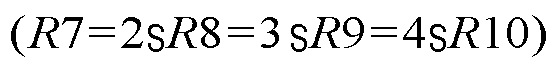
바람직하게는 상기 특정 저항들은 다음과 같은 관계를 갖는다.Preferably, the specific resistors have the following relationship.

따라서, 상기 온도 신호 출력부(130)로 부터 전송된 특정 온도 신호(예를 들어, HT<1>)가 인가되면, 상기 스위칭 소자(SW7)가 턴온되어, 반전단자와 상기 저항(R7)을 접속시키고 그에 따라 제3 온도 전압(2Vbe1)이 증폭된다. Therefore, when a specific temperature signal (for example, HT <1>) transmitted from the temperature
상기 고온 증폭부(432)의 출력전압에 대한 수식은 다음과 같다.The formula for the output voltage of the


상기 고온 온도 범위 신호 출력부(434)는 상기 고온 증폭부(432)의 출력과 기준 전압(Vbg)을 비교하여 외부 온도가 상기 온도 신호가 특정하는 온도보다 높은지 여부에 대한 신호를 출력한다. 이를 위해, 상기 기준 전압(Vbg)을 비반전 단자(+)로 입력받고, 상기 증폭된 제3 온도 전압(2Vbe1)을 반전 단자(-)로 입력받으며, 온도 범위 신호를 출력하는 OP 앰프(OP434)를 포함한다.The high temperature temperature range
따라서, 상기 고온 증폭부(432)의 출력보다 상기 기준 전압(Vbg)이 더 크면, 외부 온도가 상기 온도 신호가 특정하는 온도보다 더 높다는 의미의 하이 레벨의 고온 온도 범위 신호(H_OUT)를 출력한다. Therefore, when the reference voltage Vbg is greater than the output of the
도면을 참조하여 상기 고온 증폭부(432)와 고온 온도 범위 신호 출력부(434)의 동작을 상세히 살펴보기로 한다.An operation of the
도 8은 본원 발명의 온도 감지회로의 동작 원리를 도시한 그래프이다.8 is a graph showing the operating principle of the temperature sensing circuit of the present invention.
가로축은 현재 온도를 나타내며, 세로축은 전압 레벨을 나타낸다.The horizontal axis represents the current temperature and the vertical axis represents the voltage level.
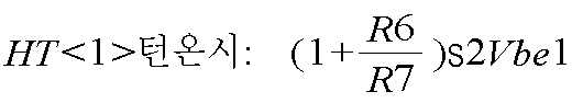
현재 온도가 HT<1>와 HT<2>의 범위에 있다고 가정하면, 기준 전압이 제3 온도 전압(2Vbe1)보다 더 크므로, 온도 신호 출력 제어부(420)는 하이레벨의 인에이블 신호(Logic_EN)를 출력한다. 상기 신호에 의하여 온도 신호 출력부(130)가 동작하게 되며, 먼저 제1 고온 신호(HT<1>)를 출력한다. 제1 고온 신호(HT<1>)에 응답하여, 상기 고온 증폭부(432)의 스위칭 소자(SW7)가 턴온되고, 제3 온도 전압(2Vbe1)이 ![]()
![]()
이 신호에 응답하여, 상기 온도 신호 출력부(130)는 제2 고온 신호(HT<2>)를 출력하고, 이에 응답하여 상기 고온 증폭부(432)의 스위칭 소자(SW8)가 턴온되고, 제3 온도 전압(2Vbe1)이 ![]()
![]()
상기 저온 온도 범위 판단부(440)는 상기 온도 신호 출력부(130)의 온도 신호에 따라 제3 온도 전압(2Vbe1)을 일정 레벨로 감소시키는 방식으로 증폭시키는 저온 증폭부(442)와, 상기 감소된 제3 온도 전압(2Vbe1)과 기준 전압(Vbg)의 크기 를 비교하여 상기 기준 전압이 더 큰 경우 상기 온도 신호 출력부의 구동을 제어하는 신호를 출력하는 저온 온도 범위 신호 출력부(446)를 포함한다. 바람직하게는, 상기 저온 온도 범위 신호 출력부는 상기 기준 전압이 더 작은 경우 상기 특정 저온 신호보다 더 낮은 온도 범위를 나타내는 저온 신호가 출력되도록 하는 하이 레벨의 저온 온도 범위 신호를 출력한다.The low temperature temperature
또한, 저온 온도 범위 판단부(440)의 동작 초기에 하이 레벨의 저온 온도 범위 신호(L_OUT)가 출력되도록 상기 저온 온도 범위 신호 출력부(446)에 기준 전압(Vbg) 보다 큰 전원전압(Vcc)을 인가하는 초기화부(444)를 더 포함한다.In addition, the power supply voltage Vcc greater than the reference voltage Vbg to the low temperature temperature range
상기 저온 증폭부(442)는 직렬 접속된 저항을 통하여 상기 제3 온도 전압(2Vbe1)을 분배하는 구조를 사용한다. 즉, 특정 온도 신호(LT<4:1>)에 따라 전압 분배 비율이 조절되는 직렬 접속된 복수 개의 저항(R1~R5), 상기 특정 온도 신호(LT<4:1>)에 응답하여 상기 저항들 사이의 특정 접속 노드를 선택하여 분배 비율을 조절하는 복수 개의 스위칭 소자들(SW1~SW4)을 포함한다. The
바람직하게는, 상기 저온 증폭부(442)는 상기 복수의 저온 신호 중 더 낮은 온도를 나타내는 저온 신호가 입력된 경우 상기 제3 온도 전압의 감소량이 더 커지도록 전압 분배 비율을 조절한다.Preferably, the low
바람직하게는, 상기 저항들은 다음과 같은 관계를 갖는다.Preferably, the resistors have the following relationship.
![]()
![]()
바람직하게는, 상기 제3 온도 전압(2Vbe1)을 안정적으로 인가하도록 제3 온도 전압(2Vbe1)을 비반전 단자(+)로 입력받고, 반전 단자(-)와 출력단이 접속된 OP 앰프(OP442)를 포함할 수 있다. Preferably, the OP amplifier OP442 receives the third temperature voltage 2Vbe1 through the non-inverting terminal (+) to stably apply the third temperature voltage 2Vbe1, and is connected to the inverting terminal (−) and the output terminal. It may include.
따라서, 상기 온도 신호 출력부(130)로부터 전송된 특정 온도 신호(예를 들어, LT<1>)가 인가되면, 상기 스위칭 소자(SW1)가 턴온되어, 상기 저항(R1)과 상기 저항(R2)의 접속노드를 선택하여 그에 따라 제3 온도 전압(2Vbe1)이 분배된다.Therefore, when a specific temperature signal (for example, LT <1>) transmitted from the temperature
상기 저온 증폭부(442)의 출력전압에 대한 수식은 다음과 같다.The formula for the output voltage of the


상기 저온 온도 범위 신호 출력부(446)는 상기 저온 증폭부(442)의 출력과 기준 전압(Vbg)을 비교하여 외부 온도가 상기 온도 신호가 특정하는 온도보다 높은지 여부에 대한 신호를 출력한다. The low temperature temperature range
이를 위해, 상기 기준 전압(Vbg)을 비반전 단자(+)로 입력받고, 상기 증폭된 제3 온도 전압(2Vbe1)을 반전 단자(-)로 입력받으며, 온도 범위 신호를 출력하는 OP 앰프(OP446)와, 상기 OP 앰프(OP446)의 출력을 반전시키는 인버터(IV446)를 포함한다. To this end, the OP amplifier OP446 that receives the reference voltage Vbg through the non-inverting terminal +, receives the amplified third temperature voltage 2Vbe1 through the inverting terminal −, and outputs a temperature range signal. And an inverter IV446 for inverting the output of the OP amplifier OP446.
따라서, 상기 고온 증폭부(442)의 출력보다 상기 기준 전압(Vbg)이 더 크면, 외부 온도가 상기 온도 신호가 특정하는 온도보다 더 낮다는 의미의 하이레벨의 저온 온도 범위 신호(L_OUT)를 출력한다. Accordingly, when the reference voltage Vbg is greater than the output of the
한편, 상기 초기화부(444)는 온도 감지 장치의 구동 신호(TS_EN)와 상기 구동 신호를 일정시간 딜레이 시킨 신호를 입력으로 하며, 초기화 제어신호(PRE)를는 출력하는 배타적 논리합 게이트(XOR)와 상기 초기화 제어신호(PRE)에 응답하여 상기 저온 온도 범위 신호 출력부(446)에 전원전압(Vcc)을 공급하는 NMOS 트랜지스터를 포함한다. 상기 초기화부(444)의 동작을 도면을 참조하여 살펴보기로 한다.The
도 5는 상기 초기화부 제어신호의 생성과정을 도시한 파형도이다.5 is a waveform diagram illustrating a process of generating the initialization control signal.
온도 감지 장치의 구동 신호(TS_EN)와 상기 구동 신호를 일정시간 딜레이 시킨 신호(delay)를 배타적 논리합 시키면 도시된 바와 같은 제어신호(PRE)가 출력되며, 상기 제어 신호가 하이 레벨이 되면, 상기 NMOS 트랜지스터를 턴온시켜 저온 온도 범위 신호 출력부(446)에 전원전압(Vcc)을 공급하게 된다. 상기 저온 온도 범 위 신호 출력부(446)는 기준전압보다 큰 전원전압(Vcc)이 인가될 경우 하이레벨의 저온 온도 범위 신호를 출력함으로써 초기화된다. When the exclusive OR of the driving signal TS_EN of the temperature sensing device and the signal delayed by the driving signal for a predetermined time is output, the control signal PRE as shown is outputted, and when the control signal becomes high level, the NMOS The transistor is turned on to supply the power supply voltage Vcc to the low temperature temperature range
도 8을 참조하여 상기 저온 증폭부(442)와 저온 온도 범위 신호 출력부(446)의 동작을 상세히 살펴보기로 한다.An operation of the
현재 온도가 LT<1>와 LT<2>의 범위에 있다고 가정하면, 기준 전압이 제3 온도 전압(2Vbe1)보다 더 작으므로, 온도 신호 출력 제어부(420)는 로우레벨의 인에이블 신호(Logic_EN)를 출력한다. 상기 신호에 의하여 온도 신호 출력부(130)가 동작하게 되며, 먼저 제1 저온 신호(LT<1>)를 출력한다. 제1 저온 신호(LT<1>)에 응답하여, 상기 저온 증폭부(442)의 스위칭 소자(SW1)가 턴온되고, 제3 온도 전압(2Vbe1)이 ![]()
![]()
이 신호에 응답하여, 상기 온도 신호 출력부(130)는 제2 저온 신호(LT<2>)를 출력하고, 이에 응답하여 상기 저온 증폭부(442)의 스위칭 소자(SW2)가 턴온되고, 제3 온도 전압(2Vbe1)이 ![]()
![]()
정리하면, 온도 범위 판단부(120)는 상기 비교 대상 전압 출력부(110)로부터 비교 대상 전압인 기준 전압(Vbg)과 제3 온도 전압(2Vbe1)을 입력받아 외부온도의 상태를 판단한다.In summary, the temperature
즉, 기준 전압(Vbg)이 더 큰 경우에는 외부 온도가 고온인 것으로 판단하고 제3 온도 전압(2Vbe1)을 일정량 증가시켜 다시 그 크기를 비교하고, 그 결과에 따라 제3 온도 전압(2Vbe1)을 상기 증가시킨 량보다 더 크게 증가시킨다.That is, when the reference voltage Vbg is larger, it is determined that the external temperature is a high temperature, the third temperature voltage 2Vbe1 is increased by a certain amount, and the magnitude is compared again. Increase greater than the increased amount.
한편, 기준 전압(Vbg)이 더 작은 경우에는 외부 온도가 저온인 것으로 판단하고 제3 온도 전압(2Vbe1)을 일정량 감소시켜 다시 그 크기를 비교하고, 그 결과에 따라 제3 온도 전압(2Vbe1)을 상기 감소시킨 량보다 더 크게 감소시킨다.On the other hand, when the reference voltage Vbg is smaller, it is determined that the external temperature is low temperature, the third temperature voltage 2Vbe1 is decreased by a certain amount, and the magnitude is compared again. Decrease more than the reduced amount.
이제 상기 온도 신호 출력부(130)의 구성과 동작을 살펴보기로 한다.Now, the configuration and operation of the temperature
도 6는 상기 온도 신호 출력부의 내부 구성을 도시한 회로도이다.6 is a circuit diagram showing an internal configuration of the temperature signal output unit.
상기 온도 신호 출력부(130)는 복수 개의 고온 신호 중 외부 온도의 범위를 나타내는 특정 고온 신호를 일정구간 동안 출력하는 고온 신호 출력부(620)와, 상기 복수 개의 저온 신호 중 외부 온도의 범위를 나타내는 특정 저온 신호를 일정구간 동안 출력하는 저온 신호 출력부(640)와, 온도 범위 판단부(120)가 출력하는 인에이블 신호(Logic_EN), 외부 온도 감지 장치의 구동 신호(TS_EN) 및 상기 고온 온도 범위 신호(H_OUT)에 응답하여 상기 고온 신호 출력부를 구동시키는 고온 신호 출력 구동부(610)와, 상기 인에이블 신호(Logic_EN)를 반전시킨 신호, 상기 외부 온도 감지 장치의 구동 신호(TS_EN) 및 상기 저온 온도 범위 신호(L_OUT)에 응답하여 상기 저온 신호 출력부를 구동시키는 저온 신호 출력 구동부(630)를 포함한다.The temperature
상기 고온 신호 출력 구동부(610)는 온도 감지 장치의 구동 신호(TS_EN), 온도 범위 판단부(120)가 출력하는 인에이블 신호(Logic_EN) 및 고온 온도 범위신호(H_OUT)를 입력받아 고온 신호 출력부(620)를 구동하는 인에이블 신호(H_EN)를 출력한다.The high temperature
상기 구동 신호(TS_EN)와 인에이블 신호(Logic_EN)를 입력으로 하는 논리곱 게이트(AND612), 상기 논리곱 게이트(AND612)의 출력과 고온 온도 범위신호(H_OUT)를 입력으로 하는 논리곱 게이트(AND614)를 포함한다. 따라서, 상기 구동 신호(TS_EN), 인에이블 신호(Logic_EN) 및 고온 온도 범위신호(H_OUT)가 모두 하이 레벨인 경우에 한하여 상기 고온 신호 출력부(620)를 구동하는 하이레벨의 인에이블 신호(H_EN)를 출력한다.AND gate AND612, which receives the driving signal TS_EN and enable signal Logic_EN, AND gate AND614, which receives the output of the AND gate AND612 and the high temperature temperature range signal H_OUT. ). Accordingly, the high level enable signal H_EN driving the high temperature
상기 저온 신호 출력 구동부(630)는 온도 감지 장치의 구동 신호(TS_EN), 온도 범위 판단부(120)가 출력하는 인에이블 신호(Logic_EN) 및 저온 온도 범위신호(L_OUT)를 입력받아 저온 신호 출력부(640)를 구동하는 인에이블 신호(L_EN)를 출력한다.The low temperature
상기 인에이블 신호(Logic_EN)가 로우 레벨일 때 동작하므로, 로우 레벨 인에이블 신호(Logic_EN) 신호를 반전시키는 인버터(IV630), 상기 구동 신호(TS_EN) 와 반전된 인에이블 신호(Logic_EN)를 입력으로 하는 논리곱 게이트(AND632), 상기 논리곱 게이트(AND632)의 출력과 저온 온도 범위신호(L_OUT)를 입력으로 하는 논리곱 게이트(AND634)를 포함한다. 따라서, 상기 구동 신호(TS_EN), 반전된 인에이블 신호(Logic_EN) 및 저온 온도 범위신호(H_OUT)가 모두 하이 레벨인 경우에 한하여 상기 저온 신호 출력부(640)를 구동하는 하이레벨의 인에이블 신호(L_EN)를 출력한다.Since the operation is performed when the enable signal Logic_EN is at the low level, the inverter IV630 for inverting the low level enable signal Logic_EN and the drive signal TS_EN and the inverted enable signal Logic_EN are inputted. An AND gate AND632, and an AND gate having an output of the AND gate AND632 and a low temperature temperature range signal L_OUT as an input. Accordingly, the high level enable signal for driving the low temperature
상기 고온 신호 출력부(620)는 상기 하이레벨의 인에이블 신호(H_EN), 클럭신호(CLK), 리셋신호(Reset) 등을 입력으로 하며, 고온 신호 출력 구동 신호(H_EN)가 하이 레벨을 유지하는 동안, 상기 복수의 고온 신호를 온도가 증가하는 순으로 일정 기간 동안 하이 레벨로 유지시킨다. 즉, 외부 온도를 지정하는 복수의 고온 신호들(HT<4:1>)을 온도가 증가하는 순서대로(HT<1>, HT<2>, HT<3>, HT<4>) 출력한다. 상기 고온 신호들은 본원 발명의 온도 감지 장치의 출력 신호가 되거나, 상기 온도 범위 판단부(120)에 포함된 고온 증폭부(432)의 특정 저항들을 OP 앰프(OP432)의 반전단자(-)로 접속시키는 제어신호로서의 역할을 한다. The high temperature
또한, 상기 저온 신호 출력부(640)는 상기 하이레벨의 인에이블 신호(L_EN), 클럭신호(CLK), 리셋신호(Reset) 등을 입력으로 하며, 저온 신호 출력 구동 신호(L_EN)가 하이 레벨을 유지하는 동안, 상기 복수의 저온 신호를 온도가 감소하는 순으로 일정 기간 동안 하이 레벨로 유지킨다. 즉, 외부 온도를 지정하는 복수의 저온 신호들(LT<4:1>)을 온도가 감소하는 순서대로(LT<1>, LT<2>, LT<3>, LT<4>) 출력한다. 상기 저온 신호들은 본원 발명의 온도 감지 장치의 출력 신호가 되거나, 상기 온도 범위 판단부(120)에 포함된 저온 증폭부(442)의 특정 저항들간의 접속 노드를 선택하는 역할을 한다.In addition, the low temperature
상기 고온 신호 출력부(620)와 저온 신호 출력부(640)의 구성은 거의 동일하며, 이에 대한 상세 구성을 살펴보기로 한다.The configuration of the high temperature
도 7a는 고온 신호 출력부 또는 저온 신호 출력부의 동작을 도시한 도면이다.7A is a diagram illustrating an operation of a high temperature signal output unit or a low temperature signal output unit.
상기 고온 신호 출력부 또는 저온 신호 출력부(이하, '신호 출력부(600)'라 한다)는 복수 개의 D 플립플롭이 접속된 쉬프트 레지스터를 포함한다. 간단을 위하여 테스트 신호가 총 네 개인 경우를 도시하고 있다.The high temperature signal output unit or the low temperature signal output unit (hereinafter, referred to as a signal output unit 600) includes a shift register to which a plurality of D flip-flops are connected. For simplicity, a total of four test signals are shown.
상기 신호출력부(600)는 하이 레벨의 인에이블 신호(H_EN, L_EN)가 인가되는 동안 동작을 하며, 클럭신호의 라이징 에지에서 하이레벨의 온도 신호(HT<n> 또는 LT<n>)를 출력한다. 도시된 바와 같이, 클럭신호가 상승하는 시점에서 하이 레벨의 온도 신호가 순차적으로 출력된다. The
다만, 인에이블 신호가 로우 레벨로 천이 되면 천이되는 순간의 온도 신호가 일정구간 동안 하이 레벨을 유지하게 된다. 이와 같이 일정구간 동안 하이 레벨이 유지되는 신호가 현재의 외부 온도를 나타내는 신호가 되며, 이 신호가 외부 온도 감지 장치의 출력이된다. 바람직하게는, 하이 레벨이 유지되는 다른 온도 신호에 비하여 2배 이상의 시간동안 하이레벨이 유지되도록 한다. 이후, 하이 레벨의 리셋(Reset) 신호가 인가되면, 클럭신호의 상승 시점에서 각 온도 신호는 로우 레벨 로 초기화된다. 이와 같이, 외부 온도의 범위를 나타내는 신호가 출력되며, 이를 통하여 외부 온도 범위를 나타내는 코드 신호를 형성할 수 있다.However, when the enable signal transitions to the low level, the temperature signal at the instant of transition maintains the high level for a certain period. As such, a signal in which the high level is maintained for a certain period becomes a signal indicating the current external temperature, and this signal becomes the output of the external temperature sensing device. Preferably, the high level is maintained for two or more times as compared to other temperature signals at which the high level is maintained. Thereafter, when a high level reset signal is applied, each temperature signal is initialized to a low level at the time when the clock signal rises. As such, a signal indicating a range of the external temperature is output, and through this, a code signal indicating the range of the external temperature may be formed.
도 7b는 상기 신호 출력부의 동작을 도시한 파형도이다. 7B is a waveform diagram illustrating the operation of the signal output unit.
현재 온도가 HT<2>와 HT<3>의 범위에 있다고 가정하면, 기준 전압이 제3 온도 전압(2Vbe1)보다 더 크므로, 온도 신호 출력 제어부(420)는 하이레벨의 인에이블 신호(Logic_EN)를 출력한다. 상기 신호에 의하여 온도 신호 출력부(130)가 동작하게 되며, 먼저 제1 고온 신호(HT<1>)를 출력한다(t1 시점). 제1 고온 신호(HT<1>)에 응답하여, 상기 고온 증폭부(432)의 스위칭 소자(SW7)가 턴온되고, 제3 온도 전압(2Vbe1)이 ![]()
![]()
이 신호에 응답하여, 상기 온도 신호 출력부(130)는 제2 고온 신호(HT<2>)를 출력하고(t2 시점), 이에 응답하여 상기 고온 증폭부(432)의 스위칭 소자(SW8)가 턴온되고, 제3 온도 전압(2Vbe1)이 ![]()
![]()
이 신호에 응답하여, 상기 온도 신호 출력부(130)는 제3 고온 신호(HT<3>)를 출력하고(t3 시점), 이에 응답하여 상기 고온 증폭부(432)의 스위칭 소자(SW9)가 턴온되고, 제3 온도 전압(2Vbe1)이 ![]()
![]()
정리하면, 상기 온도 신호 출력부(130)는 온도 범위 판단부(120)의 출력 신호에 응답하여, 특정의 고온 신호 또는 저온 신호를 외부로 출력하거나, 상기 온도 범위 판단부(120)로 피드백 입력시킨다. In summary, the temperature
전술한 본원 발명의 구성에 따라, 외부 온도의 범위를 나타내는 코드 신호를 형성할 수 있다. 이렇게 형성된 코드 신호를 이용하여 반도체의 셀 동작에 영향을 미치는 전압이나 클록 등에 변화를 줄 수 있는 코드 신호를 생성하여 이용할 수 있다. 또한, 퓨즈를 컷팅 방식의 온도 감지 장치에 비하여 퓨즈를 컷팅하는데 소요되는 시간을 줄일수 있어 제품을 테스트하는데 시간을 절약하는 효과가 있다. According to the above-described configuration of the present invention, a code signal representing a range of external temperature can be formed. The code signal formed as described above may be used to generate and use a code signal capable of changing a voltage, a clock, or the like that affects the cell operation of the semiconductor. In addition, the time taken to cut the fuse can be reduced compared to the temperature sensing device of the fuse type, thereby saving time in testing the product.
Claims (26)
Priority Applications (2)
| Application Number | Priority Date | Filing Date | Title |
|---|---|---|---|
| KR1020070015351A KR100816150B1 (en) | 2007-02-14 | 2007-02-14 | Temperature sensing device |
| US11/949,666 US8371749B2 (en) | 2007-02-14 | 2007-12-03 | Temperature sensor |
Applications Claiming Priority (1)
| Application Number | Priority Date | Filing Date | Title |
|---|---|---|---|
| KR1020070015351A KR100816150B1 (en) | 2007-02-14 | 2007-02-14 | Temperature sensing device |
Publications (1)
| Publication Number | Publication Date |
|---|---|
| KR100816150B1 true KR100816150B1 (en) | 2008-03-21 |
Family
ID=39411479
Family Applications (1)
| Application Number | Title | Priority Date | Filing Date |
|---|---|---|---|
| KR1020070015351A Expired - Fee Related KR100816150B1 (en) | 2007-02-14 | 2007-02-14 | Temperature sensing device |
Country Status (2)
| Country | Link |
|---|---|
| US (1) | US8371749B2 (en) |
| KR (1) | KR100816150B1 (en) |
Families Citing this family (8)
| Publication number | Priority date | Publication date | Assignee | Title |
|---|---|---|---|---|
| US7441949B2 (en) * | 2005-12-16 | 2008-10-28 | Micron Technology, Inc. | System and method for providing temperature data from a memory device having a temperature sensor |
| US7780346B2 (en) * | 2007-10-31 | 2010-08-24 | Texas Instruments Incorporated | Methods and apparatus for a fully isolated NPN based temperature detector |
| KR100898654B1 (en) * | 2007-12-28 | 2009-05-22 | 주식회사 하이닉스반도체 | Temperature sensing device |
| KR101439849B1 (en) * | 2008-02-01 | 2014-09-17 | 삼성전자주식회사 | Apparatus for sensing temperature of an inkjet head |
| US7724068B1 (en) * | 2008-12-03 | 2010-05-25 | Micrel, Incorporated | Bandgap-referenced thermal sensor |
| JP2010224594A (en) * | 2009-03-19 | 2010-10-07 | Oki Semiconductor Co Ltd | Voltage generation circuit |
| US9939330B2 (en) | 2014-03-28 | 2018-04-10 | Darryl G. Walker | Semiconductor device having subthreshold operating circuits including a back body bias potential based on temperature range |
| TWI558095B (en) * | 2014-05-05 | 2016-11-11 | 瑞昱半導體股份有限公司 | Clock generation circuit and method thereof |
Citations (3)
| Publication number | Priority date | Publication date | Assignee | Title |
|---|---|---|---|---|
| JPH02202219A (en) * | 1989-01-31 | 1990-08-10 | Mitsubishi Electric Corp | temperature detection circuit |
| KR960002357A (en) * | 1994-06-24 | 1996-01-26 | 김주용 | Sense amplifier |
| KR19990018175A (en) * | 1997-08-26 | 1999-03-15 | 윤종용 | Temperature detection circuit and static ram device |
Family Cites Families (27)
| Publication number | Priority date | Publication date | Assignee | Title |
|---|---|---|---|---|
| US4390874A (en) * | 1981-01-09 | 1983-06-28 | Texas Instruments Incorporated | Liquid crystal display system having improved temperature compensation |
| US4575806A (en) * | 1982-03-26 | 1986-03-11 | Gould, Inc. | Precision temperature measuring system |
| JPS6149616A (en) * | 1984-08-10 | 1986-03-11 | シーメンス、アクチエンゲゼルシヤフト | Temperature protection circuit device |
| US4859834A (en) * | 1988-06-15 | 1989-08-22 | Letco Management Company, Inc. | Power controller for heat tracing cable which responds to ambient temperature |
| JP3361422B2 (en) * | 1995-12-15 | 2003-01-07 | 日本特殊陶業株式会社 | Engine start control method and apparatus |
| US6956337B2 (en) * | 2003-08-01 | 2005-10-18 | Directed Electronics, Inc. | Temperature-to-color converter and conversion method |
| US7180211B2 (en) * | 2003-09-22 | 2007-02-20 | Micro Technology, Inc. | Temperature sensor |
| US7266031B2 (en) * | 2003-11-19 | 2007-09-04 | Infineon Technologies Ag | Internal voltage generator with temperature control |
| DE10358357A1 (en) * | 2003-12-12 | 2005-07-21 | Infineon Technologies Ag | Temperature load detector for integrated semiconductor chip during soldering, has chip containing temperature sensor measuring magnitude |
| US7171327B2 (en) * | 2004-03-24 | 2007-01-30 | Infineon Technologies Ag | Temperature sensor scheme |
| US7674035B2 (en) * | 2004-09-15 | 2010-03-09 | Nxp B.V. | Digital temperature sensors and calibration thereof |
| US7102417B2 (en) * | 2004-11-05 | 2006-09-05 | International Business Machines Corporation | Integrated circuit die including a temperature detection circuit, and system and methods for calibrating the temperature detection circuit |
| US7197421B2 (en) * | 2004-11-30 | 2007-03-27 | Broadcom Corporation | Method and system for a temperature sensor for transmitter output power compensation |
| US7427158B2 (en) * | 2005-01-13 | 2008-09-23 | Kabushiki Kaisha Toshiba | Advanced thermal sensor |
| US7197420B2 (en) * | 2005-02-04 | 2007-03-27 | International Business Machines Corporation | Method and apparatus for on-chip dynamic temperature tracking |
| US7225099B1 (en) * | 2005-02-10 | 2007-05-29 | Xilinx, Inc. | Apparatus and method for temperature measurement using a bandgap voltage reference |
| US7471583B2 (en) * | 2005-09-29 | 2008-12-30 | Hynix Semiconductor Inc. | Memory device with self refresh cycle control function |
| US7443176B2 (en) * | 2005-11-22 | 2008-10-28 | Stmicroelectronics, Inc. | Test mode and test method for a temperature tamper detection circuit |
| US7441949B2 (en) * | 2005-12-16 | 2008-10-28 | Micron Technology, Inc. | System and method for providing temperature data from a memory device having a temperature sensor |
| JP4807074B2 (en) * | 2005-12-28 | 2011-11-02 | Tdk株式会社 | Temperature detection circuit and temperature detection method |
| JP2007192718A (en) * | 2006-01-20 | 2007-08-02 | Oki Electric Ind Co Ltd | Temperature sensor |
| JP2007263709A (en) * | 2006-03-28 | 2007-10-11 | Fujitsu Ltd | Temperature characteristic correction method and sensor amplification circuit |
| JP4949013B2 (en) * | 2006-04-03 | 2012-06-06 | ハイニックス セミコンダクター インク | Semiconductor memory device having temperature sensing device and driving method thereof |
| US7603249B1 (en) * | 2006-04-19 | 2009-10-13 | Darryl Walker | Semiconductor device having variable parameter selection based on temperature and test method |
| US7686508B2 (en) * | 2006-10-21 | 2010-03-30 | Intersil Americas Inc. | CMOS temperature-to-digital converter with digital correction |
| US20080169866A1 (en) * | 2007-01-16 | 2008-07-17 | Zerog Wireless, Inc. | Combined charge storage circuit and bandgap reference circuit |
| US7724068B1 (en) * | 2008-12-03 | 2010-05-25 | Micrel, Incorporated | Bandgap-referenced thermal sensor |
-
2007
- 2007-02-14 KR KR1020070015351A patent/KR100816150B1/en not_active Expired - Fee Related
- 2007-12-03 US US11/949,666 patent/US8371749B2/en active Active
Patent Citations (3)
| Publication number | Priority date | Publication date | Assignee | Title |
|---|---|---|---|---|
| JPH02202219A (en) * | 1989-01-31 | 1990-08-10 | Mitsubishi Electric Corp | temperature detection circuit |
| KR960002357A (en) * | 1994-06-24 | 1996-01-26 | 김주용 | Sense amplifier |
| KR19990018175A (en) * | 1997-08-26 | 1999-03-15 | 윤종용 | Temperature detection circuit and static ram device |
Also Published As
| Publication number | Publication date |
|---|---|
| US8371749B2 (en) | 2013-02-12 |
| US20080192804A1 (en) | 2008-08-14 |
Similar Documents
| Publication | Publication Date | Title |
|---|---|---|
| KR100816150B1 (en) | Temperature sensing device | |
| US7127368B2 (en) | On-chip temperature sensor for low voltage operation | |
| US7953569B2 (en) | On die thermal sensor of semiconductor memory device and method thereof | |
| JP4406405B2 (en) | Temperature sensing system | |
| JP4807074B2 (en) | Temperature detection circuit and temperature detection method | |
| TWI317133B (en) | Negative voltage generator | |
| US10429417B2 (en) | Brown-out detectors | |
| KR100888483B1 (en) | Reference bias circuit compensates for process variation | |
| US8283609B2 (en) | On die thermal sensor in semiconductor memory device | |
| JP2008084514A (en) | Temperature information output device | |
| US7834680B2 (en) | Internal voltage generation circuit for generating stable internal voltages withstanding varying external conditions | |
| US20080191673A1 (en) | Series regulator circuit | |
| TWI651609B (en) | Low voltage locking circuit and device thereof integrated with reference voltage generating circuit | |
| KR20130123903A (en) | Reference voltage generator | |
| US7703975B2 (en) | Temperature detecting circuit | |
| US7528644B2 (en) | Temperature detecting circuit | |
| JP2009176111A (en) | Band-gap reference voltage source circuit | |
| KR100792370B1 (en) | Internal voltage generator | |
| KR101173482B1 (en) | Temperature compensation type oscillator | |
| US9620177B2 (en) | Internal power supply circuit, semiconductor device, and semiconductor device manufacturing method | |
| KR100569555B1 (en) | Temperature sensing circuit | |
| KR100795006B1 (en) | Offset voltage measuring device | |
| KR100898654B1 (en) | Temperature sensing device | |
| KR100650727B1 (en) | Voltage generator for memory device | |
| KR101575814B1 (en) | level detector |
Legal Events
| Date | Code | Title | Description |
|---|---|---|---|
| A201 | Request for examination | ||
| PA0109 | Patent application |
St.27 status event code: A-0-1-A10-A12-nap-PA0109 |
|
| PA0201 | Request for examination |
St.27 status event code: A-1-2-D10-D11-exm-PA0201 |
|
| P11-X000 | Amendment of application requested |
St.27 status event code: A-2-2-P10-P11-nap-X000 |
|
| P13-X000 | Application amended |
St.27 status event code: A-2-2-P10-P13-nap-X000 |
|
| D13-X000 | Search requested |
St.27 status event code: A-1-2-D10-D13-srh-X000 |
|
| D14-X000 | Search report completed |
St.27 status event code: A-1-2-D10-D14-srh-X000 |
|
| E701 | Decision to grant or registration of patent right | ||
| PE0701 | Decision of registration |
St.27 status event code: A-1-2-D10-D22-exm-PE0701 |
|
| GRNT | Written decision to grant | ||
| PR0701 | Registration of establishment |
St.27 status event code: A-2-4-F10-F11-exm-PR0701 |
|
| PR1002 | Payment of registration fee |
St.27 status event code: A-2-2-U10-U11-oth-PR1002 Fee payment year number: 1 |
|
| PG1601 | Publication of registration |
St.27 status event code: A-4-4-Q10-Q13-nap-PG1601 |
|
| PR1001 | Payment of annual fee |
St.27 status event code: A-4-4-U10-U11-oth-PR1001 Fee payment year number: 4 |
|
| PR1001 | Payment of annual fee |
St.27 status event code: A-4-4-U10-U11-oth-PR1001 Fee payment year number: 5 |
|
| PN2301 | Change of applicant |
St.27 status event code: A-5-5-R10-R13-asn-PN2301 St.27 status event code: A-5-5-R10-R11-asn-PN2301 |
|
| PN2301 | Change of applicant |
St.27 status event code: A-5-5-R10-R13-asn-PN2301 St.27 status event code: A-5-5-R10-R11-asn-PN2301 |
|
| FPAY | Annual fee payment |
Payment date: 20130225 Year of fee payment: 6 |
|
| PR1001 | Payment of annual fee |
St.27 status event code: A-4-4-U10-U11-oth-PR1001 Fee payment year number: 6 |
|
| FPAY | Annual fee payment |
Payment date: 20140221 Year of fee payment: 7 |
|
| PR1001 | Payment of annual fee |
St.27 status event code: A-4-4-U10-U11-oth-PR1001 Fee payment year number: 7 |
|
| FPAY | Annual fee payment |
Payment date: 20150223 Year of fee payment: 8 |
|
| PR1001 | Payment of annual fee |
St.27 status event code: A-4-4-U10-U11-oth-PR1001 Fee payment year number: 8 |
|
| PN2301 | Change of applicant |
St.27 status event code: A-5-5-R10-R13-asn-PN2301 St.27 status event code: A-5-5-R10-R11-asn-PN2301 |
|
| FPAY | Annual fee payment |
Payment date: 20160223 Year of fee payment: 9 |
|
| PR1001 | Payment of annual fee |
St.27 status event code: A-4-4-U10-U11-oth-PR1001 Fee payment year number: 9 |
|
| FPAY | Annual fee payment |
Payment date: 20170223 Year of fee payment: 10 |
|
| PR1001 | Payment of annual fee |
St.27 status event code: A-4-4-U10-U11-oth-PR1001 Fee payment year number: 10 |
|
| FPAY | Annual fee payment |
Payment date: 20180223 Year of fee payment: 11 |
|
| PR1001 | Payment of annual fee |
St.27 status event code: A-4-4-U10-U11-oth-PR1001 Fee payment year number: 11 |
|
| FPAY | Annual fee payment |
Payment date: 20190220 Year of fee payment: 12 |
|
| PR1001 | Payment of annual fee |
St.27 status event code: A-4-4-U10-U11-oth-PR1001 Fee payment year number: 12 |
|
| FPAY | Annual fee payment |
Payment date: 20200226 Year of fee payment: 13 |
|
| PR1001 | Payment of annual fee |
St.27 status event code: A-4-4-U10-U11-oth-PR1001 Fee payment year number: 13 |
|
| PR1001 | Payment of annual fee |
St.27 status event code: A-4-4-U10-U11-oth-PR1001 Fee payment year number: 14 |
|
| PR1001 | Payment of annual fee |
St.27 status event code: A-4-4-U10-U11-oth-PR1001 Fee payment year number: 15 |
|
| PC1903 | Unpaid annual fee |
St.27 status event code: A-4-4-U10-U13-oth-PC1903 Not in force date: 20230318 Payment event data comment text: Termination Category : DEFAULT_OF_REGISTRATION_FEE |
|
| PC1903 | Unpaid annual fee |
St.27 status event code: N-4-6-H10-H13-oth-PC1903 Ip right cessation event data comment text: Termination Category : DEFAULT_OF_REGISTRATION_FEE Not in force date: 20230318 |
|
| P22-X000 | Classification modified |
St.27 status event code: A-4-4-P10-P22-nap-X000 |