KR100810613B1 - Memory module with improved arrangement of individual elements - Google Patents
Memory module with improved arrangement of individual elements Download PDFInfo
- Publication number
- KR100810613B1 KR100810613B1 KR1020060073664A KR20060073664A KR100810613B1 KR 100810613 B1 KR100810613 B1 KR 100810613B1 KR 1020060073664 A KR1020060073664 A KR 1020060073664A KR 20060073664 A KR20060073664 A KR 20060073664A KR 100810613 B1 KR100810613 B1 KR 100810613B1
- Authority
- KR
- South Korea
- Prior art keywords
- memory
- disposed
- tabs
- region
- individual
- Prior art date
- Legal status (The legal status is an assumption and is not a legal conclusion. Google has not performed a legal analysis and makes no representation as to the accuracy of the status listed.)
- Expired - Fee Related
Links
Images


Classifications
-
- H10W90/00—
-
- H—ELECTRICITY
- H05—ELECTRIC TECHNIQUES NOT OTHERWISE PROVIDED FOR
- H05K—PRINTED CIRCUITS; CASINGS OR CONSTRUCTIONAL DETAILS OF ELECTRIC APPARATUS; MANUFACTURE OF ASSEMBLAGES OF ELECTRICAL COMPONENTS
- H05K1/00—Printed circuits
- H05K1/18—Printed circuits structurally associated with non-printed electric components
- H05K1/181—Printed circuits structurally associated with non-printed electric components associated with surface mounted components
-
- G—PHYSICS
- G06—COMPUTING OR CALCULATING; COUNTING
- G06F—ELECTRIC DIGITAL DATA PROCESSING
- G06F1/00—Details not covered by groups G06F3/00 - G06F13/00 and G06F21/00
-
- G—PHYSICS
- G11—INFORMATION STORAGE
- G11C—STATIC STORES
- G11C5/00—Details of stores covered by group G11C11/00
- G11C5/02—Disposition of storage elements, e.g. in the form of a matrix array
- G11C5/04—Supports for storage elements, e.g. memory modules; Mounting or fixing of storage elements on such supports
-
- H—ELECTRICITY
- H05—ELECTRIC TECHNIQUES NOT OTHERWISE PROVIDED FOR
- H05K—PRINTED CIRCUITS; CASINGS OR CONSTRUCTIONAL DETAILS OF ELECTRIC APPARATUS; MANUFACTURE OF ASSEMBLAGES OF ELECTRICAL COMPONENTS
- H05K1/00—Printed circuits
- H05K1/02—Details
- H05K1/0213—Electrical arrangements not otherwise provided for
- H05K1/0216—Reduction of cross-talk, noise or electromagnetic interference
- H05K1/023—Reduction of cross-talk, noise or electromagnetic interference using auxiliary mounted passive components or auxiliary substances
-
- H—ELECTRICITY
- H05—ELECTRIC TECHNIQUES NOT OTHERWISE PROVIDED FOR
- H05K—PRINTED CIRCUITS; CASINGS OR CONSTRUCTIONAL DETAILS OF ELECTRIC APPARATUS; MANUFACTURE OF ASSEMBLAGES OF ELECTRICAL COMPONENTS
- H05K2201/00—Indexing scheme relating to printed circuits covered by H05K1/00
- H05K2201/09—Shape and layout
- H05K2201/09818—Shape or layout details not covered by a single group of H05K2201/09009 - H05K2201/09809
- H05K2201/09954—More mounting possibilities, e.g. on same place of PCB, or by using different sets of edge pads
-
- H—ELECTRICITY
- H05—ELECTRIC TECHNIQUES NOT OTHERWISE PROVIDED FOR
- H05K—PRINTED CIRCUITS; CASINGS OR CONSTRUCTIONAL DETAILS OF ELECTRIC APPARATUS; MANUFACTURE OF ASSEMBLAGES OF ELECTRICAL COMPONENTS
- H05K2201/00—Indexing scheme relating to printed circuits covered by H05K1/00
- H05K2201/10—Details of components or other objects attached to or integrated in a printed circuit board
- H05K2201/10007—Types of components
- H05K2201/10159—Memory
-
- H—ELECTRICITY
- H05—ELECTRIC TECHNIQUES NOT OTHERWISE PROVIDED FOR
- H05K—PRINTED CIRCUITS; CASINGS OR CONSTRUCTIONAL DETAILS OF ELECTRIC APPARATUS; MANUFACTURE OF ASSEMBLAGES OF ELECTRICAL COMPONENTS
- H05K2203/00—Indexing scheme relating to apparatus or processes for manufacturing printed circuits covered by H05K3/00
- H05K2203/15—Position of the PCB during processing
- H05K2203/1572—Processing both sides of a PCB by the same process; Providing a similar arrangement of components on both sides; Making interlayer connections from two sides
-
- H10W90/724—
-
- Y—GENERAL TAGGING OF NEW TECHNOLOGICAL DEVELOPMENTS; GENERAL TAGGING OF CROSS-SECTIONAL TECHNOLOGIES SPANNING OVER SEVERAL SECTIONS OF THE IPC; TECHNICAL SUBJECTS COVERED BY FORMER USPC CROSS-REFERENCE ART COLLECTIONS [XRACs] AND DIGESTS
- Y02—TECHNOLOGIES OR APPLICATIONS FOR MITIGATION OR ADAPTATION AGAINST CLIMATE CHANGE
- Y02P—CLIMATE CHANGE MITIGATION TECHNOLOGIES IN THE PRODUCTION OR PROCESSING OF GOODS
- Y02P70/00—Climate change mitigation technologies in the production process for final industrial or consumer products
- Y02P70/50—Manufacturing or production processes characterised by the final manufactured product
Landscapes
- Engineering & Computer Science (AREA)
- Microelectronics & Electronic Packaging (AREA)
- Theoretical Computer Science (AREA)
- Physics & Mathematics (AREA)
- General Engineering & Computer Science (AREA)
- General Physics & Mathematics (AREA)
- Semiconductor Memories (AREA)
- Structures For Mounting Electric Components On Printed Circuit Boards (AREA)
- Dram (AREA)
Abstract
개별소자들의 개선된 배치 구조를 갖는 메모리 모듈이 제공된다. 상기 메모리 모듈은 기판 본체 및 복수의 탭들(tabs)을 구비한다. 상기 탭들은 상기 기판 본체의 적어도 일면 가장자리에 배치된다. 상기 탭들과 같은 면에 메모리 패드 영역 및 개별소자들(discrete devices)이 배치된다. 상기 메모리 패드 영역은 상기 탭들과 전기적으로 접속된 메모리 칩 패드들을 갖는다. 상기 메모리 칩 패드들은 메모리 칩의 단자 영역에 배치된 복수의 단자들에 대응하도록 배열될 수 있다. 상기 개별소자들은 상기 메모리 패드 영역 주변의 어느 하나의 방향에 국한하여 배치된다. 또한, 상기 개별소자들은 상기 탭들 및 상기 메모리 칩 패드들과 전기적으로 접속된다.
A memory module having an improved arrangement of individual elements is provided. The memory module has a substrate body and a plurality of tabs. The tabs are disposed at at least one edge of the substrate body. The memory pad area and discrete devices are disposed on the same side as the tabs. The memory pad area has memory chip pads electrically connected to the tabs. The memory chip pads may be arranged to correspond to a plurality of terminals disposed in the terminal area of the memory chip. The individual devices are disposed in one direction around the memory pad area. In addition, the individual devices are electrically connected to the tabs and the memory chip pads.
Description
도 1은 종래기술에 의한 메모리 모듈의 부품배치를 보여주는 평면도이다.1 is a plan view showing a component arrangement of a memory module according to the prior art.
도 2는 본 발명의 실시 예에 따른 메모리 모듈의 실장된 모습을 보여주는 사시도이다.2 is a perspective view illustrating a mounted state of a memory module according to an embodiment of the present invention.
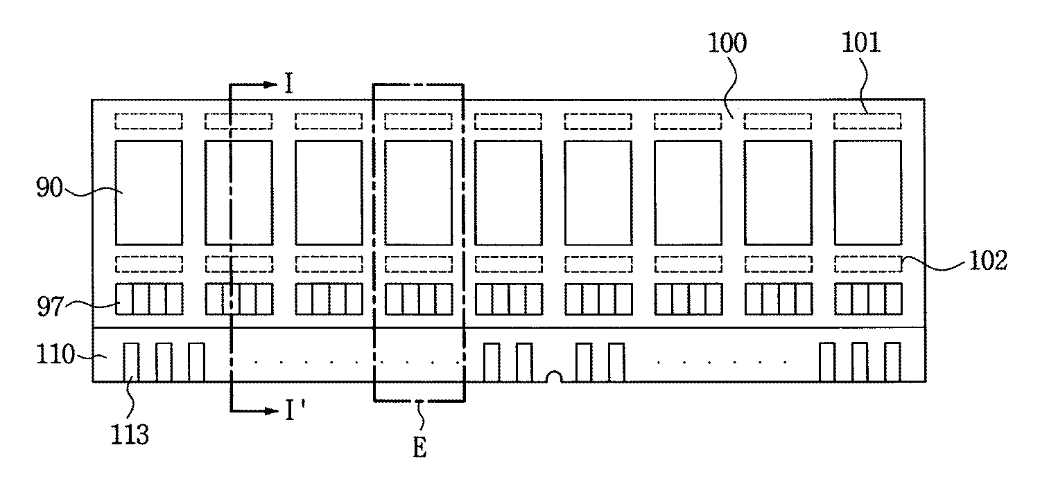
도 3은 본 발명의 실시 예에 따른 메모리 모듈의 부품배치를 보여주는 평면도이다.3 is a plan view illustrating a component arrangement of a memory module according to an embodiment of the present invention.
도 4는 도 3의 E 부분에 적용된 인쇄회로기판을 보여주는 평면도이다.4 is a plan view illustrating a printed circuit board applied to the portion E of FIG. 3.
도 5는 본 발명의 실시 예에 따른 메모리 모듈을 설명하기 위하여 도 3의 절단선 I-I'에 따라 취해진 단면도이다.5 is a cross-sectional view taken along the line II ′ of FIG. 3 to describe a memory module according to an example embodiment of the inventive concept.
도 6 및 도 7은 본 발명의 실시 예에 따른 메모리 모듈에 사용되는 메모리 칩들의 후면을 보여주는 평면도들이다.6 and 7 are plan views illustrating rear surfaces of memory chips used in a memory module according to an embodiment of the present invention.
도 8 내지 도 13은 본 발명의 다른 실시 예들에 따른 메모리 모듈의 부품배치를 보여주는 평면도들이다.8 to 13 are plan views illustrating component arrangements of memory modules according to other example embodiments of the inventive concepts.
도 14 내지 도 16은 본 발명의 또 다른 실시 예들에 따른 메모리 모듈을 설명하기 위한 단면도들이다.14 through 16 are cross-sectional views illustrating memory modules in accordance with some example embodiments of the inventive concepts.
**도면의 주요부분에 대한 부호의 설명**** Description of the symbols for the main parts of the drawings **
11, 100, 200, 300, 400, 500, 600, 700 : 기판 본체11, 100, 200, 300, 400, 500, 600, 700: substrate body
13, 113 : 탭(tab) 110 : 탭 영역13, 113: tab 110: tab area
60 : 외부장치 63 : 소켓60: external device 63: socket
15, 15', 90, 90' : 메모리 칩15, 15 ', 90, 90': memory chip
95 : 단자 영역 95B : 단자95:
195 : 메모리 패드 영역195: memory pad area
195P : 메모리 칩 패드195P: Memory Chip Pads
17, 97 : 개별소자들(discrete devices)17, 97: discrete devices
97B : 개별소자 단자97B: Individual element terminal
197 : 개별소자 패드 영역197: individual device pad area
197P : 개별소자 패드197P: Individual Device Pads
101, 102, 201, 302, 401, 402, 501, 602, 701, 702 : 완충 영역101, 102, 201, 302, 401, 402, 501, 602, 701, 702: buffer area
116 : 내부 배선116: internal wiring
SP : 아래 영역 NP : 위 영역SP: Lower Area NP: Upper Area
WP : 왼쪽 영역 EP : 오른쪽 영역WP: left area EP: right area
본 발명은 반도체장치에 관한 것으로, 특히 개별소자들의 개선된 배치 구조를 갖는 메모리 모듈에 관한 것이다.The present invention relates to a semiconductor device, and more particularly to a memory module having an improved arrangement of individual elements.
개인용 컴퓨터, 시스템 서버, 및 통신기기 등 다수의 전자시스템들은 데이터의 저장장치로서 메모리 모듈을 채택하고 있다. 상기 메모리 모듈은 인쇄회로기판(printed circuit board)에 부착된 메모리 칩들 및 개별소자들(discrete devices)을 구비한다. 상기 인쇄회로기판에는 외부 커넥터에 전기적으로 접속하기 위한 탭들(tabs)이 제공된다.Many electronic systems, such as personal computers, system servers, and communication devices, employ memory modules as data storage devices. The memory module includes memory chips and discrete devices attached to a printed circuit board. The printed circuit board is provided with tabs for electrically connecting to an external connector.
상기 메모리 칩들은 디램(DRAM) 또는 에스램(SRAM)과 같은 휘발성 메모리소자를 구비한다. 상기 개별소자들은 저항(resistor), 커패시터(capacitor), 인덕터(inductor), 레지스터(register), 프로그래머블 소자(programmable device), 또는 비 휘발성 메모리소자(non-volatile memory device)일 수 있다. 상기 개별소자들은 상기 탭들에 인가되는 외부 신호들을 상기 메모리 칩들에 저장할 수 있도록 분배하는 역할을 한다. 상기 메모리 칩들에 저장된 데이터는 상기 개별소자들을 경유하여 읽어낼 수 있다.The memory chips include volatile memory devices such as DRAM or SRAM. The individual devices may be a resistor, a capacitor, an inductor, a register, a programmable device, or a non-volatile memory device. The individual devices distribute the external signals applied to the taps to be stored in the memory chips. Data stored in the memory chips can be read out through the individual devices.
도 1은 종래의 메모리 모듈을 설명하기 위한 평면도이다.1 is a plan view illustrating a conventional memory module.
도 1을 참조하면, 종래의 메모리 모듈은 기판 본체(11)에 부착된 메모리 칩들(15) 및 개별소자들(17)을 구비한다. 상기 기판 본체(11)의 가장자리에 탭들(tabs; 13)이 배치된다. 상기 기판 본체(11) 및 상기 탭들(13)은 인쇄회로기판을 구성한다.Referring to FIG. 1, a conventional memory module includes
상기 기판 본체(11)는 통상적으로 4층 내지 8층의 기판들을 접착하여 형성한 다층 기판 구조가 널리 사용된다. 상기 탭들(13)은 상기 기판 본체(11)의 내부에 형성된 배선들을 통하여 상기 메모리 칩들(15) 및 상기 개별소자들(17)과 전기적으로 접속될 수 있다. 또한, 상기 탭들(13)은 상기 메모리 칩들(15) 및 상기 개별소자들(17)을 외부장치에 전기적으로 접속해주는 역할을 한다.The substrate
상기 메모리 칩들(15)은 상기 기판 본체(11)의 장축을 따라 일렬로 배열된다. 도시된 바와 같이, 상기 개별소자들(17)은 상기 각각의 메모리 칩들(15) 주변에 배치된다. 그런데 상기 메모리 칩들(15)은 고집적화 및 대용량화에 따라 다양한 크기를 구비할 수 있다. 예를 들면, 대용량 메모리 칩(15')은 상기 메모리 칩들(15) 보다 큰 외부치수를 가질 수 있다. 이 경우에, 상기 개별소자들(17)은 상기 대용량 메모리 칩(15')을 상기 기판 본체(11)에 장착하는 것을 방해한다.The
상기 대용량 메모리 칩(15')을 상기 기판 본체(11)에 배치하려면 상기 개별소자들(17)의 위치를 변경하여야 한다. 즉, 종래의 메모리 모듈은 상기 메모리 칩들(15)의 크기에 따라 서로 다른 규격의 인쇄회로기판을 필요로 한다.In order to arrange the large-
한편, 메모리 모듈에 관한 다른 형성방법이 일본공개특허 제 2005-251971호에 "메모리 실장방법(MOUNTING METHOD OF MEMORY, AND MEMORY MODULE MOUNTED BY MOUNTING METHOD)"이라는 제목으로 고바야시 가수아끼 등(KOBAYASHI KATSUAKI et al.)에 의해 개시된 바 있다.On the other hand, another method for forming a memory module is disclosed in Japanese Patent Laid-Open Publication No. 2005-251971 entitled “MOUNTING METHOD OF MEMORY, AND MEMORY MODULE MOUNTED BY MOUNTING METHOD”. .).
고바야시 가수아끼 등에 따르면, 소정 길이의 인쇄회로기판 위에 서로 다른 사양의 메모리 칩들을 부착할 수 있게 하는 메모리 칩의 실장 방법 및 그 실장 방법에 의하여 형성되는 메모리 모듈이 제공된다. 그런데 상기 메모리 모듈은 저 항(resistor), 커패시터(capacitor), 및 레지스터(register)와 같은 개별소자들을 필요로 한다. 상기 개별소자들은 상기 메모리 칩들의 효율적인 배치를 제한할 수 있다.According to Kobayashi Kaiseki et al., There is provided a memory chip mounting method and a memory module formed by the mounting method that enable attaching memory chips of different specifications on a printed circuit board of a predetermined length. However, the memory module requires individual elements such as a resistor, a capacitor, and a register. The discrete devices can limit the efficient placement of the memory chips.
결론적으로, 상기 개별소자들 및 상기 메모리 칩들을 보다 효율적으로 배치하는 기술이 필요하다.In conclusion, there is a need for a technique for more efficiently disposing the individual elements and the memory chips.
본 발명이 이루고자 하는 기술적 과제는 상술한 종래기술의 문제점을 개선하기 위한 것으로서, 동일규격의 인쇄회로기판에 서로 다른 크기의 메모리 칩 장착이 가능한 메모리 모듈을 제공하는 데 있다.SUMMARY OF THE INVENTION The present invention has been made in an effort to improve the above-described problems of the related art, and to provide a memory module capable of mounting memory chips of different sizes on a printed circuit board of the same standard.
상기 기술적 과제를 달성하기 위하여 본 발명은, 개별소자들의 개선된 배치 구조를 갖는 메모리 모듈을 제공한다. 상기 메모리 모듈은 기판 본체 및 복수의 탭들(tabs)을 구비한다. 상기 탭들은 상기 기판 본체의 적어도 일면 가장자리에 배치된다. 상기 탭들과 같은 면에 메모리 패드 영역 및 개별소자들(discrete devices)이 배치된다. 상기 메모리 패드 영역은 상기 탭들과 전기적으로 접속된 메모리 칩 패드들을 갖는다. 상기 개별소자들은 상기 메모리 패드 영역 주변의 어느 하나의 방향에 국한하여 배치된다. 또한, 상기 개별소자들은 상기 탭들 및 상기 메모리 칩 패드들과 전기적으로 접속된다.In order to achieve the above technical problem, the present invention provides a memory module having an improved arrangement of individual elements. The memory module has a substrate body and a plurality of tabs. The tabs are disposed at at least one edge of the substrate body. The memory pad area and discrete devices are disposed on the same side as the tabs. The memory pad area has memory chip pads electrically connected to the tabs. The individual devices are disposed in one direction around the memory pad area. In addition, the individual devices are electrically connected to the tabs and the memory chip pads.
본 발명의 몇몇 실시 예들에 있어서, 상기 메모리 패드 영역은 상기 개별소자들로부터 소정 거리 이격된 것일 수 있다.In some embodiments of the present disclosure, the memory pad area may be spaced apart from the individual elements by a predetermined distance.
다른 실시 예들에 있어서, 상기 메모리 패드 영역은 상기 기판 본체의 가장자리로부터 소정 거리 이격된 것일 수 있다.In example embodiments, the memory pad area may be spaced apart from the edge of the substrate body by a predetermined distance.
또 다른 실시 예들에 있어서, 상기 개별소자들은 상기 탭들 및 상기 메모리 패드 영역 사이에 배치되는 것일 수 있다.In other embodiments, the individual devices may be disposed between the tabs and the memory pad area.
또 다른 실시 예들에 있어서, 상기 개별소자들은 상기 탭들의 반대편 가장자리에 배치되는 것일 수 있다.In still other embodiments, the individual devices may be disposed on opposite edges of the tabs.
또 다른 실시 예들에 있어서, 상기 메모리 패드 영역에 메모리 칩이 장착될 수 있다.In other embodiments, a memory chip may be mounted in the memory pad area.
또 다른 실시 예들에 있어서, 상기 메모리 칩 패드들은 상기 메모리 칩의 단자 영역에 배치된 복수의 단자들에 대응하도록 배열된 것일 수 있다.In still other embodiments, the memory chip pads may be arranged to correspond to a plurality of terminals disposed in a terminal area of the memory chip.
또 다른 실시 예들에 있어서, 상기 개별소자들(discrete devices)은 저항(resistor), 커패시터(capacitor), 인덕터(inductor), 레지스터(register), 프로그래머블 소자(programmable device), 및 비 휘발성 메모리소자(non-volatile memory device)로 이루어진 일군에서 선택된 하나를 포함하는 것일 수 있다.In still other embodiments, the discrete devices may include a resistor, a capacitor, an inductor, a register, a programmable device, and a nonvolatile memory device. It may include one selected from the group consisting of -volatile memory device).
또한, 본 발명은, 복수의 메모리 패드 영역들을 갖는 메모리 모듈을 제공한다. 상기 메모리 모듈은 기판 본체 및 복수의 탭들(tabs)을 구비한다. 상기 탭들은 상기 기판 본체의 적어도 일면 가장자리에 배치된다. 상기 탭들과 같은 면에 복수의 메모리 패드 영역들 및 개별소자들(discrete devices)이 배치된다. 상기 메모리 패드 영역들은 상기 기판 본체의 장축을 따라 서로 이격되도록 배치된다. 상기 메모리 패드 영역들은 상기 탭들과 전기적으로 접속된 메모리 칩 패드들을 갖는다. 상기 개별소자들은 상기 각각의 메모리 패드 영역들 주변의 어느 하나의 방향에 국한하여 배치된다. 또한, 상기 개별소자들은 상기 탭들 및 상기 메모리 칩 패드들과 전기적으로 접속된다.The present invention also provides a memory module having a plurality of memory pad regions. The memory module has a substrate body and a plurality of tabs. The tabs are disposed at at least one edge of the substrate body. A plurality of memory pad regions and discrete devices are disposed on the same side as the tabs. The memory pad regions are disposed to be spaced apart from each other along the long axis of the substrate body. The memory pad regions have memory chip pads electrically connected to the tabs. The individual elements are disposed in one direction around each of the memory pad regions. In addition, the individual devices are electrically connected to the tabs and the memory chip pads.
몇몇 실시 예들에 있어서, 상기 메모리 패드 영역들은 나란히 배치된 것일 수 있다.In some embodiments, the memory pad regions may be arranged side by side.
다른 실시 예들에 있어서, 상기 메모리 패드 영역들은 서로 어긋나게 배치된 것일 수 있다. 이 경우에, 상기 메모리 패드 영역들 중 적어도 하나와 상기 탭들 사이에 상기 개별소자들이 배치될 수 있다. 상기 메모리 패드 영역들 중 적어도 다른 하나에 있어서는 상기 탭들의 반대편 가장자리에 상기 개별소자들이 배치될 수 있다.In other embodiments, the memory pad regions may be disposed to be offset from each other. In this case, the individual devices may be disposed between at least one of the memory pad regions and the tabs. In at least one of the memory pad regions, the individual elements may be disposed at opposite edges of the tabs.
또 다른 실시 예들에 있어서, 상기 개별소자들은 상기 탭들 및 상기 메모리 패드 영역들 사이에 배치될 수 있다.In other embodiments, the individual devices may be disposed between the tabs and the memory pad areas.
또 다른 실시 예들에 있어서, 상기 개별소자들은 상기 탭들의 반대편 가장자리에 배치될 수 있다.In still other embodiments, the individual devices may be disposed at opposite edges of the tabs.
또 다른 실시 예들에 있어서, 상기 메모리 패드 영역들은 상기 개별소자들로부터 소정 거리 이격된 것일 수 있다.In still other embodiments, the memory pad regions may be spaced apart from the individual elements by a predetermined distance.
또 다른 실시 예들에 있어서, 상기 메모리 패드 영역들은 상기 기판 본체의 가장자리로부터 소정 거리 이격된 것일 수 있다.In example embodiments, the memory pad regions may be spaced apart from the edge of the substrate body by a predetermined distance.
또 다른 실시 예들에 있어서, 상기 메모리 패드 영역들은 상기 기판 본체의 전면 및 후면에 배치될 수 있다. 상기 전면의 메모리 패드 영역들 및 상기 후면의 메모리 패드 영역들은 서로 어긋나게 배치될 수 있다.In other embodiments, the memory pad regions may be disposed on the front and rear surfaces of the substrate body. The memory pad regions of the front surface and the memory pad regions of the rear surface may be disposed to be offset from each other.
또 다른 실시 예들에 있어서, 상기 전면의 개별소자들은 상기 탭들의 반대편 가장자리에 배치되고, 상기 후면의 개별소자들은 상기 탭들 및 상기 메모리 패드 영역들 사이에 배치되는 것일 수 있다.In another embodiment, individual elements on the front side may be disposed at opposite edges of the tabs, and individual elements on the rear side may be disposed between the tabs and the memory pad regions.
이하, 첨부한 도면들을 참조하여 본 발명의 바람직한 실시 예들을 상세히 설명하기로 한다. 그러나 본 발명은 여기서 설명되어지는 실시 예들에 한정되지 않고 다른 형태로 구체화될 수도 있다. 오히려, 여기서 소개되는 실시 예들은 개시된 내용이 철저하고 완전해질 수 있도록 그리고 당업자에게 본 발명의 사상이 충분히 전달될 수 있도록 하기 위해 제공되어지는 것이다. 도면들에 있어서, 층 및 영역들의 두께는 명확성을 기하기 위하여 과장되어진 것이다. 또한, 층이 다른 층 또는 기판 "상"에 있다고 언급되어지는 경우에 그것은 다른 층 또는 기판 상에 직접 형성될 수 있거나 또는 그들 사이에 제 3의 층이 개재될 수도 있다. 명세서 전체에 걸쳐서 동일한 참조번호로 표시된 부분들은 동일한 구성요소들을 의미한다.Hereinafter, exemplary embodiments of the present invention will be described in detail with reference to the accompanying drawings. However, the present invention is not limited to the embodiments described herein and may be embodied in other forms. Rather, the embodiments introduced herein are provided to ensure that the disclosed contents are thorough and complete, and that the spirit of the present invention to those skilled in the art will fully convey. In the drawings, the thicknesses of layers and regions are exaggerated for clarity. In addition, where a layer is said to be "on" another layer or substrate, it may be formed directly on the other layer or substrate, or a third layer may be interposed therebetween. Portions denoted by like reference numerals denote like elements throughout the specification.
도 2는 본 발명의 제 1 실시 예에 따른 메모리 모듈의 실장된 모습을 보여주는 사시도이고, 도 3은 본 발명의 제 1 실시 예에 따른 메모리 모듈의 부품배치를 보여주는 평면도이다. 도 4는 도 3의 E 부분에 적용된 인쇄회로기판을 보여주는 평면도이고, 도 5는 본 발명의 제 1 실시 예에 따른 메모리 모듈을 설명하기 위하여 도 3의 절단선 I-I'에 따라 취해진 단면도이다. 도 6 및 도 7은 본 발명의 실시 예 에 따른 메모리 모듈에 사용되는 메모리 칩들의 후면을 보여주는 평면도들이다.2 is a perspective view illustrating a mounted state of a memory module according to a first embodiment of the present invention, and FIG. 3 is a plan view illustrating a component arrangement of the memory module according to the first embodiment of the present invention. 4 is a plan view illustrating a printed circuit board applied to the portion E of FIG. 3, and FIG. 5 is a cross-sectional view taken along the line II ′ of FIG. 3 to describe a memory module according to the first embodiment of the present disclosure. . 6 and 7 are plan views illustrating rear surfaces of memory chips used in a memory module according to an embodiment of the present invention.
도 2를 참조하면, 본 발명의 제 1 실시 예에 따른 메모리 모듈은 기판 본체(100), 메모리 칩들(90) 및 개별소자들(discrete devices; 97)을 구비할 수 있다. 상기 메모리 모듈은 소켓(63)에 장착되어 외부장치(60)와 전기적으로 접속될 수 있다.Referring to FIG. 2, the memory module according to the first embodiment of the present invention may include a
개인용 컴퓨터, 시스템 서버, 및 통신기기 등 다수의 전자시스템들에 있어서, 상기 메모리 모듈은 그들의 데이터 저장장치로서 널리 채택될 수 있다. 예를 들면, 상기 외부장치(60)는 개인용 컴퓨터의 메인 보드(main board)일 수 있다. 상기 소켓(63)은 상기 메인 보드(main board)에 나란히 배치된 여러 개일 수 있다. 상기 외부장치(60)는 상기 소켓들(63)을 통하여 상기 메모리 모듈에 데이터를 저장하고 읽어낼 수 있다.In many electronic systems such as personal computers, system servers, and communication devices, the memory modules can be widely adopted as their data storage devices. For example, the
상기 기판 본체(100)는 장축을 갖는 얇은 판 모양일 수 있다. 상기 기판 본체(100)는 상기 소켓(63)에 삽입하기에 적합한 두께를 구비할 수 있다. 상기 메모리 칩들(90)은 상기 기판 본체(100)의 장축을 따라 일렬로 배치될 수 있다. 상기 메모리 칩들(90)은 디램(DRAM) 또는 에스램(SRAM)과 같은 휘발성 메모리소자(volatile memory device)를 구비할 수 있다.The substrate
상기 개별소자들(97)은 상기 메모리 칩들(90) 각각의 한쪽에 국한하여 배치될 수 있다. 상기 개별소자들(97)은 저항(resistor), 커패시터(capacitor), 인덕터(inductor), 레지스터(register), 프로그래머블 소자(programmable device), 및 비 휘발성 메모리소자(non-volatile memory device)로 이루어진 일군에서 선택된 하나를 포함할 수 있다. 상기 개별소자들(97)은 상기 메모리 칩들(90)에 입출력되는 데이터들을 분배하는 역할을 할 수 있다.The
도 3을 참조하면, 상기 기판 본체(100)의 일면 가장자리에 탭 영역(110)이 배치될 수 있다. 상기 탭 영역(110)에 복수의 탭들(tabs; 113)이 제공될 수 있다. 즉, 상기 기판 본체(100)의 일면 가장자리에 상기 탭들(113)이 배치될 수 있다. 상기 메모리 칩들(90)은 상기 탭들(113)과 같은 면에 상기 기판 본체(100)의 장축을 따라 일렬로 장착될 수 있다. 상기 메모리 칩들(90) 및 상기 탭 영역(110) 사이에 상기 개별소자들(97)이 배치될 수 있다. 상기 개별소자들(97)은 상기 메모리 칩들(90) 및 상기 탭들(113)과 전기적으로 접속될 수 있다.Referring to FIG. 3, a
상기 기판 본체(100)는 얇은 판 모양일 수 있다. 상기 탭들(113)은 상기 기판 본체(100)의 양면에 각각 제공될 수 있다. 상기 탭 영역(110)은 상기 소켓들(63) 중 선택된 하나에 삽입될 수 있다. 상기 탭들(113)은 구리와 같은 도전성 물질막일 수 있다. 이 경우에, 상기 탭들(113)은 상기 외부장치(60) 및 상기 메모리 칩들(90) 사이를 전기적으로 접속해주는 역할을 할 수 있다.The
상기 탭 영역(110)의 반대편 가장자리에 제 1 완충영역들(101)이 배치될 수 있다. 상기 제 1 완충영역들(101)은 상기 메모리 칩들(90)을 상기 기판 본체(100)의 가장자리로부터 이격시키는 역할을 할 수 있다. 상기 메모리 칩들(90) 및 상기 개별소자들(97) 사이에 제 2 완충영역들(102)이 배치될 수 있다. 상기 제 2 완충영역들(102)은 상기 메모리 칩들(90) 및 상기 개별소자들(97) 사이를 이격시키는 역할을 할 수 있다.
이에 더하여, 상기 메모리 칩들(90) 및 상기 개별소자들(97)은 상기 기판 본체(100)의 양면에 각각 장착될 수도 있다. 상기 탭들(113) 또한 상기 기판 본체(100)의 양면에 각각 배치될 수 있다.In addition, the
도 4를 참조하면, 상기 기판 본체(100)의 일면에 메모리 패드 영역(195)이 배치될 수 있다. 상기 메모리 패드 영역(195)은 상기 탭 영역(110)과 같은 면에 배치될 수 있다. 상기 메모리 패드 영역(195)은 상기 메모리 칩(90)의 단자 영역에 대응하는 크기와 형상일 수 있다. 상기 메모리 패드 영역(195) 내에는 상기 단자 영역에 배치된 복수의 단자들에 대응하도록 배열된 메모리 칩 패드들(195P)이 제공될 수 있다. 상기 메모리 칩 패드들(195P)은 구리와 같은 도전성 물질막일 수 있다. 상기 메모리 칩 패드들(195P)은 상기 탭들(113)과 전기적으로 접속될 수 있다.Referring to FIG. 4, a
예를 들면, 상기 메모리 패드 영역(195) 내에는 84개의 상기 메모리 칩 패드들(195P)이 제공될 수 있다. 또한, 상기 메모리 패드 영역(195) 내에는 상기 단자 영역에 배치된 복수의 단자들보다 많은 수의 상기 메모리 칩 패드들(195P)이 제공될 수도 있다.For example, 84
상기 메모리 패드 영역(195)은 상기 탭 영역(110)과 이격되도록 배치될 수 있다. 상기 기판 본체(100)의 표면은 상기 메모리 패드 영역(195)을 중심으로 하여 아래, 위, 왼쪽 및 오른쪽 영역들(SP, NP, WP, EP)로 분류될 수 있다. 즉, 상기 아래 영역(SP)은 상기 메모리 패드 영역(195) 및 상기 탭 영역(110) 사이에 위치할 수 있다. 상기 위 영역(NP)은 상기 탭 영역(110) 반대편 가장자리와 상기 메모리 패드 영역(195) 사이에 위치할 수 있다. 상기 왼쪽 영역(WP)은 상기 위 영역(NP) 및 상기 아래 영역(SP) 사이의 상기 메모리 패드 영역(195) 왼쪽에 위치할 수 있다. 상기 오른쪽 영역(EP)은 상기 위 영역(NP) 및 상기 아래 영역(SP) 사이의 상기 메모리 패드 영역(195) 오른쪽에 위치할 수 있다.The
상기 메모리 패드 영역(195) 및 상기 탭 영역(110) 사이에 개별소자 패드 영역(197)이 배치될 수 있다. 즉, 상기 개별소자 패드 영역(197)은 상기 메모리 패드 영역(195)의 한쪽에 국한하여 배치될 수 있다. 상기 개별소자 패드 영역(197)에는 상기 개별소자들(97)에 대응하는 개별소자 패드들(197P)이 제공될 수 있다. 상기 개별소자 패드들(197P)은 구리와 같은 도전성 물질막일 수 있다. 상기 개별소자 패드들(197P)은 상기 메모리 칩 패드들(195P) 및 상기 탭들(113)과 전기적으로 접속될 수 있다.Individual
상기 위 영역(NP)에 제 1 완충영역(101)이 배치될 수 있다. 상기 제 1 완충영역(101)에는 상기 개별소자 패드들(197P) 또는 상기 메모리 칩 패드들(195P)이 배치되지 않는다. 즉. 상기 제 1 완충영역(101)은 상기 메모리 패드 영역(195)을 상기 기판 본체(100)의 가장자리로부터 이격시키는 역할을 할 수 있다.The
상기 메모리 패드 영역(195) 및 상기 개별소자 패드 영역(197) 사이에 제 2 완충영역(102)이 배치될 수 있다. 즉, 상기 제 2 완충영역(102)은 상기 아래 영역(SP)에 배치될 수 있다. 상기 제 2 완충영역(102)은 상기 메모리 패드 영역(195)을 상기 개별소자 패드 영역(197)으로부터 이격시키는 역할을 할 수 있다.A
상기 기판 본체(100), 상기 탭들(113), 상기 메모리 칩 패드들(195P), 및 상기 개별소자 패드들(197P)은 인쇄회로기판을 구성할 수 있다. 상기 메모리 패드 영 역(195)에 상기 메모리 칩(90)이 장착될 수 있다. 즉, 상기 메모리 패드 영역(195)에 대응하는 단자영역을 갖는 상기 메모리 칩(90)은 상기 인쇄회로기판에 장착될 수 있다. 상기 개별소자 패드 영역(197)에 상기 개별소자들(97)이 장착될 수 있다.The substrate
상기 메모리 패드 영역(195)은 상기 제 1 완충영역(101)에 의하여 상기 기판 본체(100)의 가장자리로부터 이격될 수 있다. 또한, 상기 메모리 패드 영역(195)은 상기 제 2 완충영역(102)에 의하여 상기 개별소자들(97)로부터 이격될 수 있다. 이에 따라, 상기 메모리 칩(90)은 상기 메모리 패드 영역(195)보다 큰 외부치수를 구비할지라도 상기 인쇄회로기판에 장착될 수 있다. 즉, 상기 제 1 완충영역(101) 및 상기 제 2 완충영역(102)을 갖는 상기 인쇄회로기판은 서로 다른 크기의 상기 메모리 칩(90)을 장착할 수 있는 충분한 여유를 제공할 수 있다.The
도 5를 참조하면, 상기 기판 본체(100)는 4층의 얇은 박판들을 적층하여 형성한 구조체일 수 있다. 상기 기판 본체(100)의 내부에 상기 탭들(113), 상기 메모리 칩들(90), 및 상기 개별소자들(97)을 전기적으로 접속해주는 역할을 하는 내부 배선들(116)이 제공될 수 있다. 상기 내부 배선들(116)은 구리와 같은 도전성 물질막일 수 있다. 상기 기판 본체(100), 상기 탭들(113), 상기 메모리 칩 패드들(도 4의 195P), 상기 개별소자 패드들(도 4의 197P), 및 상기 내부 배선들(116)은 인쇄회로기판을 구성할 수 있다.Referring to FIG. 5, the substrate
상기 개별소자들(97)은 개별소자 단자들(97B)에 의하여 상기 개별소자 패드들(도 4의 197P)에 부착될 수 있다. 상기 개별소자 단자들(97B)은 솔더 볼(solder ball)과 갈은 도전성 접착재료일 수 있다. 그 결과, 상기 개별소자들(97)은 상기 탭들(113)과 인접한 곳에 배치될 수 있다. 상기 개별소자들(97)은 상기 내부 배선들(116)을 통하여 상기 탭들(113) 및 상기 메모리 칩들(90)과 전기적으로 접속될 수 있다.The
상기 메모리 칩들(90)은 단자 영역에 배치된 복수의 단자들(95B)에 의하여 상기 메모리 칩 패드들(도 4의 195P)에 부착될 수 있다. 상기 단자들(95B)은 솔더 볼(solder ball)과 갈은 도전성 접착재료일 수 있다. 그 결과, 상기 메모리 칩들(90)은 상기 메모리 패드 영역(195)에 배치될 수 있다. 상기 메모리 칩들(90)은 상기 내부 배선들(116)을 통하여 상기 탭들(113) 및 상기 개별소자들(97)과 전기적으로 접속될 수 있다.The
상기 제 1 완충영역(101)은 상기 탭 영역(110)의 반대편 가장자리에 배치될 수 있다. 상기 제 2 완충영역(102)은 상기 메모리 패드 영역(195) 및 상기 개별소자들(97) 사이에 배치될 수 있다. 즉, 상기 메모리 칩(90)은 상기 제 1 완충영역(101)에 의하여 상기 기판 본체(100)의 가장자리로부터 이격될 수 있다. 또한, 상기 메모리 칩(90)은 상기 제 2 완충영역(102)에 의하여 상기 개별소자들(97)로부터 이격될 수 있다. 이에 따라, 상기 메모리 칩(90)은 상기 메모리 패드 영역(195)보다 큰 외부치수를 갖는다 하여도 상기 인쇄회로기판에 장착될 수 있다. 즉, 상기 제 1 완충영역(101) 및 상기 제 2 완충영역(102)을 갖는 상기 인쇄회로기판은 서로 다른 크기의 상기 메모리 칩(90)을 장착할 수 있는 충분한 여유를 제공할 수 있다.The
상기 메모리 칩들(90) 및 상기 개별소자들(97)은 상기 기판 본체(100)의 양면에 각각 배치될 수 있다. 상기 탭들(113) 또한 상기 기판 본체(100)의 양면에 각 각 배치될 수 있다. 이 경우에, 상기 기판 본체(100)의 양면에 각각 배치된 상기 메모리 칩들(90)은 서로 대칭되는 구조를 가질 수 있다. 이와는 달리, 상기 메모리 칩들(90)은 서로 비대칭 구조를 가질 수도 있다.The
도 6을 참조하면, 상기 메모리 칩(90)은 단자 영역(95)을 구비할 수 있다. 상기 단자 영역(95) 내에 복수의 상기 단자들(95B)이 배치될 수 있다. 상기 단자들(95B)은 솔더 볼(solder ball)과 갈은 도전성 접착재료일 수 있다. 예를 들면, 상기 단자들(95B)은 6열로 정렬된 84개의 솔더 볼(solder ball)일 수 있다. 상기 메모리 칩(90)은 상기 단자 영역(95)보다 큰 외부치수를 구비할 수 있다. 상기 단자 영역(95)은 상기 메모리 칩(90)의 후면에 배치될 수 있다.Referring to FIG. 6, the
도 7을 참조하면, 대용량 메모리 칩(90')은 상기 메모리 칩(90) 보다 상대적으로 큰 외부치수를 구비할 수 있다. 반면, 상기 대용량 메모리 칩(90')은 상기 메모리 칩(90)의 것과 동일한 크기의 상기 단자 영역(95)을 구비할 수 있다.Referring to FIG. 7, the large
도 2 내지 도 7을 통하여 설명한 바와 같이, 본 발명의 제 1 실시 예에 따른 메모리 모듈은 상기 인쇄회로기판에 장착된 상기 메모리 칩들(90) 및 상기 개별소자들(discrete devices; 97)을 구비할 수 있다. 상기 인쇄회로기판은 상기 기판 본체(100), 상기 탭들(113), 상기 내부 배선들(116), 상기 메모리 칩 패드들(195P), 및 상기 개별소자 패드들(197P)을 구비할 수 있다.As described above with reference to FIGS. 2 through 7, the memory module according to the first embodiment of the present invention may include the
상기 개별소자 패드들(197P)은 상기 탭들(113) 및 상기 메모리 칩 패드들(195P) 사이에 배치된다. 즉, 상기 개별소자들(discrete devices; 97)은 상기 메모리 칩 패드들(195P)의 한쪽에 국부적으로 배치된다. 상기 기판 본체(100)의 표면 에 상기 제 1 완충영역(101) 및 상기 제 2 완충영역(102)이 배치될 수 있다. 상기 완충영역들(101, 102) 상에는 상기 개별소자 패드들(197P)이 배치되지 않는다. 이에 따라, 다양한 크기를 갖는 상기 메모리 칩들(90)을 상기 인쇄회로기판에 장착할 수 있다. 즉, 상기 대용량 메모리 칩(90')이라 할지라도 상기 메모리 패드 영역(195)에 대응하는 상기 단자 영역(95)을 구비하는 경우 장착될 수 있다.The
도 8은 본 발명의 제 2 실시 예에 따른 메모리 모듈의 부품배치를 보여주는 평면도이다.8 is a plan view illustrating a component arrangement of a memory module according to a second embodiment of the present invention.
도 8을 참조하면, 본 발명의 제 2 실시 예에 따른 메모리 모듈은 기판 본체(200), 상기 메모리 칩들(90) 및 상기 개별소자들(discrete devices; 97)을 구비할 수 있다. 상기 기판 본체(200)의 일면 가장자리에 상기 탭 영역(110)이 배치될 수 있다. 상기 탭 영역(110)에 복수의 상기 탭들(tabs; 113)이 제공될 수 있다. 상기 메모리 칩들(90)은 상기 탭 영역(110)과 같은 면에 배치된 메모리 패드 영역(도시되지 않음)에 장착될 수 있다. 상기 개별소자들(97)은 상기 탭 영역(110)과 같은 면에 배치된 개별소자 패드 영역(도시되지 않음)에 장착될 수 있다.Referring to FIG. 8, a memory module according to the second embodiment of the present disclosure may include a
상기 개별소자들(97)은 상기 메모리 칩들(90) 및 상기 탭 영역(110) 사이에 국부적으로 배치될 수 있다. 상기 기판 본체(200)의 상기 위 영역(도 4의 NP)에 제 1 완충영역(201)이 배치될 수 있다. 상기 제 1 완충영역(201)에는 상기 개별소자들(97)이 배치되지 않는다. 상기 제 1 완충영역(201)은 상기 메모리 칩들(90)을 상기 기판 본체(200)의 가장자리로부터 이격시키는 역할을 할 수 있다. 이에 따라, 다양한 크기를 갖는 상기 메모리 칩들(90)을 상기 인쇄회로기판에 장착할 수 있다.The
도 9는 본 발명의 제 3 실시 예에 따른 메모리 모듈의 부품배치를 보여주는 평면도이다.9 is a plan view illustrating a component arrangement of a memory module according to a third embodiment of the present invention.
도 9를 참조하면, 본 발명의 제 3 실시 예에 따른 메모리 모듈은 기판 본체(300), 상기 메모리 칩들(90) 및 상기 개별소자들(discrete devices; 97)을 구비할 수 있다. 상기 기판 본체(300)의 일면 가장자리에 상기 탭 영역(110)이 배치될 수 있다. 상기 탭 영역(110)에 복수의 상기 탭들(tabs; 113)이 제공될 수 있다. 상기 메모리 칩들(90)은 상기 탭 영역(110)과 같은 면에 배치된 메모리 패드 영역들(도시되지 않음)에 장착될 수 있다. 상기 개별소자들(97)은 상기 탭 영역(110)과 같은 면에 배치된 개별소자 패드 영역들(도시되지 않음)에 장착될 수 있다.Referring to FIG. 9, a memory module according to a third embodiment of the present disclosure may include a
상기 개별소자들(97)은 상기 위 영역(도 4의 NP)에 배치될 수 있다. 즉, 상기 개별소자들(97)은 상기 기판 본체(300)의 상기 탭 영역(110) 반대편 가장자리에 국부적으로 배치될 수 있다. 상기 메모리 칩들(90) 및 상기 탭 영역(110) 사이에 제 2 완충영역(302)이 배치될 수 있다. 상기 제 2 완충영역(302)은 상기 메모리 칩들(90)을 상기 탭 영역(110)으로부터 이격시키는 역할을 할 수 있다. 이에 따라, 다양한 크기를 갖는 상기 메모리 칩들(90)을 상기 인쇄회로기판에 장착할 수 있다.The
도 10은 본 발명의 제 4 실시 예에 따른 메모리 모듈의 부품배치를 보여주는 평면도이다.10 is a plan view illustrating a component arrangement of a memory module in accordance with a fourth embodiment of the present invention.
도 10을 참조하면, 본 발명의 제 4 실시 예에 따른 메모리 모듈은 기판 본체(400), 상기 메모리 칩들(90) 및 상기 개별소자들(discrete devices; 97)을 구비할 수 있다. 상기 기판 본체(400)의 일면 가장자리에 상기 탭 영역(110)이 배치될 수 있다. 상기 탭 영역(110)에 복수의 상기 탭들(tabs; 113)이 제공될 수 있다. 상기 메모리 칩들(90)은 상기 탭 영역(110)과 같은 면에 배치된 메모리 패드 영역(도시되지 않음)에 장착될 수 있다. 상기 개별소자들(97)은 상기 탭 영역(110)과 같은 면에 배치된 개별소자 패드 영역(도시되지 않음)에 장착될 수 있다.Referring to FIG. 10, a memory module according to a fourth embodiment of the present invention may include a substrate
상기 메모리 칩들(90) 중 선택된 몇 개 및 상기 탭 영역(110) 사이에 상기 개별소자들(97)이 국부적으로 배치될 수 있다. 이 경우에, 상기 기판 본체(400)의 상기 탭 영역(110) 반대편 가장자리에 제 1 완충영역(401)이 배치될 수 있다. 즉, 상기 제 1 완충영역(401)은 상기 위 영역(도 4의 NP)에 배치될 수 있다.The
상기 메모리 칩들(90) 중 선택된 다른 몇 개 및 상기 탭 영역(110) 사이에 제 2 완충영역(402)이 배치될 수 있다. 이 경우에, 상기 개별소자들(97)은 상기 기판 본체(400)의 상기 탭 영역(110) 반대편 가장자리에 국부적으로 배치될 수 있다.A
상기 완충영역들(401, 402)은 상기 메모리 칩들(90)을 상기 기판 본체(400)의 가장자리 또는 상기 개별소자들(97)로부터 이격시키는 역할을 할 수 있다. 이에 따라, 다양한 크기를 갖는 상기 메모리 칩들(90)을 상기 인쇄회로기판에 장착할 수 있다.The
도 11은 본 발명의 제 5 실시 예에 따른 메모리 모듈의 부품배치를 보여주는 평면도이다.11 is a plan view illustrating a component arrangement of a memory module according to a fifth embodiment of the present invention.
도 11을 참조하면, 본 발명의 제 5 실시 예에 따른 메모리 모듈은 기판 본체(500), 상기 메모리 칩들(90) 및 상기 개별소자들(discrete devices; 97)을 구비할 수 있다. 상기 기판 본체(500)의 일면 가장자리에 상기 탭 영역(110)이 배치될 수 있다. 상기 탭 영역(110)에 복수의 상기 탭들(tabs; 113)이 제공될 수 있다. 상기 메모리 칩들(90)은 상기 탭 영역(110)과 같은 면에 배치된 메모리 패드 영역(도시되지 않음)에 장착될 수 있다. 상기 개별소자들(97)은 상기 탭 영역(110)과 같은 면에 배치된 개별소자 패드 영역(도시되지 않음)에 장착될 수 있다.Referring to FIG. 11, a memory module according to a fifth embodiment of the present invention may include a
상기 개별소자들(97)은 상기 기판 본체(500)의 상기 탭 영역(110) 반대편 가장자리에 국부적으로 배치될 수 있다. 상기 개별소자들(97) 및 상기 메모리 칩들(90) 사이에 제 1 완충영역(501)이 배치될 수 있다. 상기 제 1 완충영역(501)은 상기 메모리 칩들(90)을 상기 개별소자들(97)로부터 이격시키는 역할을 할 수 있다. 이에 따라, 다양한 크기를 갖는 상기 메모리 칩들(90)을 상기 인쇄회로기판에 장착할 수 있다.The
도 12는 본 발명의 제 6 실시 예에 따른 메모리 모듈의 부품배치를 보여주는 평면도이다.12 is a plan view illustrating a component arrangement of a memory module according to a sixth embodiment of the present invention.
도 12를 참조하면, 본 발명의 제 6 실시 예에 따른 메모리 모듈은 기판 본체(600), 상기 메모리 칩들(90) 및 상기 개별소자들(discrete devices; 97)을 구비할 수 있다. 상기 기판 본체(600)의 일면 가장자리에 상기 탭 영역(110)이 배치될 수 있다. 상기 탭 영역(110)에 복수의 상기 탭들(tabs; 113)이 제공될 수 있다. 상기 메모리 칩들(90)은 상기 탭 영역(110)과 같은 면에 배치된 메모리 패드 영역(도시되지 않음)에 장착될 수 있다. 상기 개별소자들(97)은 상기 탭 영역(110)과 같은 면에 배치된 개별소자 패드 영역(도시되지 않음)에 장착될 수 있다.Referring to FIG. 12, a memory module according to the sixth embodiment of the present invention may include a
상기 개별소자들(97)은 상기 메모리 칩들(90) 및 상기 탭 영역(110) 사이에 국부적으로 배치될 수 있다. 상기 메모리 칩들(90) 및 상기 개별소자들(97) 사이에 제 2 완충영역(602)이 배치될 수 있다. 상기 제 2 완충영역(602)은 상기 메모리 칩들(90)을 상기 개별소자들(97)로부터 이격시키는 역할을 할 수 있다. 이에 따라, 다양한 크기를 갖는 상기 메모리 칩들(90)을 상기 인쇄회로기판에 장착할 수 있다.The
도 13은 본 발명의 제 7 실시 예에 따른 메모리 모듈의 부품배치를 보여주는 평면도이다.13 is a plan view illustrating a component arrangement of a memory module according to a seventh embodiment of the present invention.
도 13을 참조하면, 본 발명의 제 7 실시 예에 따른 메모리 모듈은 기판 본체(700), 상기 메모리 칩들(90) 및 상기 개별소자들(discrete devices; 97)을 구비할 수 있다. 상기 기판 본체(700)의 일면 가장자리에 상기 탭 영역(110)이 배치될 수 있다. 상기 탭 영역(110)에 복수의 상기 탭들(tabs; 113)이 제공될 수 있다. 상기 메모리 칩들(90)은 상기 탭 영역(110)과 같은 면에 배치된 메모리 패드 영역(도시되지 않음)에 장착될 수 있다. 상기 개별소자들(97)은 상기 탭 영역(110)과 같은 면에 배치된 개별소자 패드 영역(도시되지 않음)에 장착될 수 있다.Referring to FIG. 13, a memory module according to a seventh embodiment of the present disclosure may include a
상기 메모리 칩들(90)은 서로 어긋나게 배치될 수 있다. 상기 메모리 칩들(90) 중 선택된 몇 개는 상기 탭 영역(110)에 인접한 곳에 배치될 수 있다. 이 경우에, 상기 기판 본체(400)의 상기 탭 영역(110) 반대편 가장자리에 상기 개별소자들(97)이 국부적으로 배치될 수 있다. 또한, 상기 개별소자들(97) 및 상기 메모리 칩들(90) 사이에 제 1 완충영역(701)이 배치될 수 있다.The
상기 메모리 칩들(90) 중 선택된 다른 몇 개 및 상기 탭 영역(110) 사이에도 상기 개별소자들(97)이 국부적으로 배치될 수 있다. 이 경우에, 상기 메모리 칩 들(90) 및 상기 개별소자들(97) 사이에 제 2 완충영역(702)이 배치될 수 있다.The
상기 완충영역들(701, 702)은 상기 메모리 칩들(90)을 상기 개별소자들(97)로부터 이격시키는 역할을 할 수 있다. 이에 따라, 다양한 크기를 갖는 상기 메모리 칩들(90)을 상기 인쇄회로기판에 장착할 수 있다.The
도 14는 본 발명의 제 8 실시 예에 따른 메모리 모듈을 설명하기 위하여 도 3의 절단선 I-I'에 따라 취해진 단면도이다.14 is a cross-sectional view taken along the line II ′ of FIG. 3 to describe a memory module according to an eighth embodiment of the inventive concept.
도 14를 참조하면, 본 발명의 제 8 실시 예에 따른 메모리 모듈은 상기 기판 본체(100), 상기 메모리 칩들(90) 및 상기 개별소자들(discrete devices; 97)을 구비할 수 있다. 상기 기판 본체(100)의 양면에 각각 상기 탭 영역(110)이 배치될 수 있다.Referring to FIG. 14, a memory module according to an eighth embodiment of the present invention may include the
본 발명의 제 8 실시 예에 따른 메모리 모듈의 일면은, 도 3 및 도 5를 통하여 기술된바 있는, 본 발명의 제 1 실시 예에 따른 메모리 모듈과 동일한 구조를 구비할 수 있다.One surface of the memory module according to the eighth embodiment of the present invention may have the same structure as the memory module according to the first embodiment of the present invention, which has been described with reference to FIGS. 3 and 5.
본 발명의 제 8 실시 예에 따른 메모리 모듈의 다른 일면에 있어서는, 상기 기판 본체(100)의 상기 탭 영역(110) 반대편 가장자리에 개별소자 패드 영역(도시되지 않음)이 배치될 수 있다. 상기 개별소자 패드 영역에 상기 개별소자들(97)이 부착될 수 있다. 즉, 상기 기판 본체(100)의 상기 탭 영역(110) 반대편 가장자리에 상기 개별소자들(97)이 국부적으로 배치될 수 있다.In another surface of the memory module according to the eighth embodiment of the present disclosure, an individual device pad region (not shown) may be disposed at an edge of the substrate
이 경우에, 상기 개별소자들(97) 및 상기 탭 영역(110) 사이에 상기 메모리 칩(90)이 배치될 수 있다. 즉, 상기 개별소자들(97) 및 상기 탭 영역(110) 사이의 상기 기판 본체(100)에 상기 메모리 패드 영역(195)이 제공될 수 있다. 상기 개별소자들(97) 및 상기 메모리 칩(90) 사이에 제 1 완충영역(101)이 배치될 수 있다. 상기 메모리 칩(90) 및 상기 탭 영역(110) 사이에 제 2 완충영역(102)이 배치될 수 있다.In this case, the
상기 기판 본체(100), 상기 탭들(113), 상기 내부 배선들(116), 상기 메모리 패드 영역(195), 및 상기 개별소자 패드 영역은 인쇄회로기판을 구성할 수 있다. 상기 기판 본체(100)의 표면에 상기 제 1 및 제 2 완충영역들(101, 102)이 배치될 수 있다.The
상기 메모리 패드 영역들(195)은 상기 제 1 및 제 2 완충영역들(101, 102)에 의하여 상기 기판 본체(100)의 가장자리 및 상기 개별소자들(97)로부터 이격될 수 있다. 이에 따라, 상기 메모리 칩들(90)은 상기 메모리 패드 영역(195)보다 큰 외부치수를 구비할지라도 상기 인쇄회로기판에 장착될 수 있다. 즉, 상기 제 1 완충영역(101) 및 상기 제 2 완충영역(102)을 갖는 상기 인쇄회로기판은 서로 다른 크기의 상기 메모리 칩(90)을 장착할 수 있는 충분한 여유를 제공할 수 있다.The
이에 더하여, 상기 양면에 각각 배치된 상기 메모리 칩들(90)은 서로 비대칭 구조를 갖는다. 이에 따라, 본 발명의 제 8 실시 예에 따른 메모리 모듈은 상기 메모리 칩들(90)에서 발생하는 열을 효율적으로 발산하는 구조가 될 수 있다.In addition, the
도 15는 본 발명의 제 9 실시 예에 따른 메모리 모듈을 설명하기 위하여 도 8의 절단선 Ⅱ-Ⅱ'에 따라 취해진 단면도이다.FIG. 15 is a cross-sectional view taken along the line II-II ′ of FIG. 8 to describe a memory module according to a ninth embodiment of the inventive concept.
도 15를 참조하면, 본 발명의 제 9 실시 예에 따른 메모리 모듈은 상기 기판 본체(200), 상기 메모리 칩들(90) 및 상기 개별소자들(discrete devices; 97)을 구비할 수 있다. 상기 기판 본체(200)의 양면에 각각 상기 탭 영역(110)이 배치될 수 있다.Referring to FIG. 15, a memory module according to a ninth embodiment may include the substrate
본 발명의 제 9 실시 예에 따른 메모리 모듈의 양면은, 도 8을 통하여 기술된 바 있는, 본 발명의 제 2 실시 예에 따른 메모리 모듈과 동일한 구조를 각각 구비할 수 있다. 상기 기판 본체(200)의 일면 가장자리에 상기 탭 영역(110)이 배치될 수 있다. 상기 탭 영역(110)에 복수의 상기 탭들(tabs; 113)이 제공될 수 있다. 상기 메모리 칩들(90)은 상기 탭 영역(110)과 같은 면에 배치된 메모리 패드 영역(195)에 장착될 수 있다. 상기 개별소자들(97)은 상기 탭 영역(110)과 같은 면에 배치된 개별소자 패드 영역(도시되지 않음)에 장착될 수 있다.Both surfaces of the memory module according to the ninth embodiment of the present invention may have the same structure as that of the memory module according to the second embodiment of the present invention, which has been described with reference to FIG. 8. The
상기 기판 본체(200), 상기 탭들(113), 상기 내부 배선들(116), 상기 메모리 패드 영역(195), 및 상기 개별소자 패드 영역은 인쇄회로기판을 구성할 수 있다. The
상기 개별소자들(97)은 상기 메모리 칩들(90) 및 상기 탭 영역(110) 사이에 국부적으로 배치될 수 있다. 상기 기판 본체(200)의 상기 위 영역(NP)에 제 1 완충영역(201)이 배치될 수 있다. 상기 제 1 완충영역(201)은 상기 메모리 칩들(90)을 상기 기판 본체(200)의 가장자리로부터 이격시키는 역할을 할 수 있다. 이에 따라, 상기 메모리 칩들(90)은 상기 메모리 패드 영역(195)보다 큰 외부치수를 구비할지라도 상기 인쇄회로기판에 장착될 수 있다.The
이에 더하여, 본 발명의 제 9 실시 예에 따른 메모리 모듈은 상기 메모리 칩들(90) 및 상기 개별소자들(97)은 종래에 비하여 상기 탭들(113)에 상대적으로 가 깝게 배치된 구조를 갖는다. 이에 따라, 상기 메모리 모듈은 낮은 노이즈 및 빠른 응답속도와 같은 우수한 전기적 특성을 보일 수 있다.In addition, the memory module according to the ninth embodiment of the present invention has a structure in which the
더 나아가서, 상기 제 1 완충영역(201)은 생략될 수 있다. 이 경우에, 상기 기판 본체(200)는 상기 제 1 완충영역(201)의 크기만큼 축소될 수도 있다. 즉, 로우 프로파일(low profile)을 갖는 메모리 모듈을 구현할 수 있다.In addition, the
도 16은 본 발명의 제 10 실시 예에 따른 메모리 모듈을 설명하기 위하여 도 11의 절단선 Ⅲ-Ⅲ'에 따라 취해진 단면도이다.FIG. 16 is a cross-sectional view taken along the line III-III ′ of FIG. 11 to describe a memory module according to a tenth embodiment of the inventive concept.
도 16을 참조하면, 본 발명의 제 10 실시 예에 따른 메모리 모듈은 상기 기판 본체(500), 상기 메모리 칩들(90) 및 상기 개별소자들(discrete devices; 97)을 구비할 수 있다. 상기 기판 본체(500)의 양면에 상기 탭 영역(110)이 배치될 수 있다.Referring to FIG. 16, a memory module according to a tenth embodiment may include the substrate
본 발명의 제 10 실시 예에 따른 메모리 모듈의 일면은, 도 11을 통하여 기술된 바 있는, 본 발명의 제 5 실시 예에 따른 메모리 모듈과 동일한 구조를 구비할 수 있다. 상기 기판 본체(500)의 일면 가장자리에 상기 탭 영역(110)이 배치될 수 있다. 상기 탭 영역(110)에 복수의 상기 탭들(tabs; 113)이 제공될 수 있다. 상기 메모리 칩들(90)은 상기 탭 영역(110)과 같은 면에 배치된 메모리 패드 영역(195)에 장착될 수 있다. 상기 개별소자들(97)은 상기 탭 영역(110)과 같은 면에 배치된 개별소자 패드 영역(도시되지 않음)에 장착될 수 있다.One surface of the memory module according to the tenth embodiment of the present invention may have the same structure as the memory module according to the fifth embodiment of the present invention, which has been described with reference to FIG. 11. The
상기 개별소자들(97)은 상기 기판 본체(500)의 상기 탭 영역(110) 반대편 가장자리에 국부적으로 배치될 수 있다. 상기 개별소자들(97) 및 상기 메모리 칩 들(90) 사이에 상기 제 1 완충영역(501)이 배치될 수 있다. 상기 제 1 완충영역(501)은 상기 메모리 칩들(90)을 상기 개별소자들(97)로부터 이격시키는 역할을 할 수 있다.The
본 발명의 제 10 실시 예에 따른 메모리 모듈의 다른 일면은, 도 8을 통하여 기술된 바 있는, 본 발명의 제 2 실시 예에 따른 메모리 모듈과 동일한 구조를 구비할 수 있다. 상기 기판 본체(500)의 가장자리에 상기 탭 영역(110)이 배치될 수 있다. 상기 탭 영역(110)에 복수의 상기 탭들(tabs; 113)이 제공될 수 있다. 상기 메모리 칩들(90)은 상기 탭 영역(110)과 같은 면에 배치된 메모리 패드 영역(195)에 장착될 수 있다. 상기 개별소자들(97)은 상기 탭 영역(110)과 같은 면에 배치된 개별소자 패드 영역(도시되지 않음)에 장착될 수 있다.The other surface of the memory module according to the tenth embodiment of the present invention may have the same structure as the memory module according to the second embodiment of the present invention, which has been described with reference to FIG. 8. The
상기 개별소자들(97)은 상기 메모리 칩들(90) 및 상기 탭 영역(110) 사이에 국부적으로 배치될 수 있다. 상기 기판 본체(500)의 상기 위 영역(도 4의 NP)에 상기 제 2 완충영역(201)이 배치될 수 있다. 상기 제 2 완충영역(201)은 상기 메모리 칩들(90)을 상기 기판 본체(500)의 가장자리로부터 이격시키는 역할을 할 수 있다. 이에 따라, 상기 메모리 칩들(90)은 상기 메모리 패드 영역(195)보다 큰 외부치수를 구비할지라도 상기 인쇄회로기판에 장착될 수 있다.The
상술한 바와 같이 본 발명에 따르면, 상기 인쇄회로기판에 장착된 메모리 칩들 및 개별소자들이 제공된다. 상기 인쇄회로기판은 기판 본체, 탭들, 내부 배선 들, 메모리 패드 영역, 및 개별소자 패드 영역을 구비한다. 상기 개별소자들은 상기 메모리 패드 영역 주변의 어느 하나의 방향에 국한하여 배치된다. 상기 메모리 칩들은 상기 메모리 패드 영역보다 큰 외부치수를 구비할지라도 상기 인쇄회로기판에 장착될 수 있다. 즉, 동일규격의 인쇄회로기판에 서로 다른 크기의 메모리 칩 장착이 가능한 메모리 모듈을 구현할 수 있다.As described above, according to the present invention, memory chips and individual devices mounted on the printed circuit board are provided. The printed circuit board includes a substrate body, tabs, internal wirings, a memory pad area, and an individual device pad area. The individual devices are disposed in one direction around the memory pad area. The memory chips may be mounted on the printed circuit board even though they have an external dimension larger than that of the memory pad region. That is, a memory module capable of mounting memory chips of different sizes on a printed circuit board of the same standard may be implemented.
Claims (22)
Priority Applications (2)
| Application Number | Priority Date | Filing Date | Title |
|---|---|---|---|
| KR1020060073664A KR100810613B1 (en) | 2006-08-04 | 2006-08-04 | Memory module with improved arrangement of individual elements |
| US11/708,591 US20080030943A1 (en) | 2006-08-04 | 2007-02-21 | Memory module having improved arrangement of discrete devices |
Applications Claiming Priority (1)
| Application Number | Priority Date | Filing Date | Title |
|---|---|---|---|
| KR1020060073664A KR100810613B1 (en) | 2006-08-04 | 2006-08-04 | Memory module with improved arrangement of individual elements |
Publications (2)
| Publication Number | Publication Date |
|---|---|
| KR20080012604A KR20080012604A (en) | 2008-02-12 |
| KR100810613B1 true KR100810613B1 (en) | 2008-03-07 |
Family
ID=39028934
Family Applications (1)
| Application Number | Title | Priority Date | Filing Date |
|---|---|---|---|
| KR1020060073664A Expired - Fee Related KR100810613B1 (en) | 2006-08-04 | 2006-08-04 | Memory module with improved arrangement of individual elements |
Country Status (2)
| Country | Link |
|---|---|
| US (1) | US20080030943A1 (en) |
| KR (1) | KR100810613B1 (en) |
Families Citing this family (3)
| Publication number | Priority date | Publication date | Assignee | Title |
|---|---|---|---|---|
| US9196314B2 (en) * | 2011-06-24 | 2015-11-24 | Inphi Corporation | Extended-height DIMM |
| KR102086775B1 (en) * | 2013-07-10 | 2020-03-09 | 삼성전자 주식회사 | Memory module improving data signal integrity |
| KR102178829B1 (en) | 2013-11-20 | 2020-11-13 | 삼성전자 주식회사 | Semiconductor memory device |
Citations (5)
| Publication number | Priority date | Publication date | Assignee | Title |
|---|---|---|---|---|
| JPH10303362A (en) | 1997-04-28 | 1998-11-13 | T I F:Kk | Memory system |
| KR20000058713A (en) * | 2000-06-22 | 2000-10-05 | 유철영 | Magenetic Oil Pressure Pump |
| KR20030021901A (en) * | 2001-09-10 | 2003-03-15 | 삼성전자주식회사 | Memory module and printed circuit board for the same |
| KR20040058417A (en) * | 2002-12-26 | 2004-07-05 | 삼성전자주식회사 | Printed circuit board for memory module and mounting soket thereof |
| KR20050012832A (en) * | 2002-06-27 | 2005-02-02 | 인텔 코오퍼레이션 | Memory buffer arrangement |
Family Cites Families (5)
| Publication number | Priority date | Publication date | Assignee | Title |
|---|---|---|---|---|
| US5530623A (en) * | 1993-11-19 | 1996-06-25 | Ncr Corporation | High speed memory packaging scheme |
| US6222739B1 (en) * | 1998-01-20 | 2001-04-24 | Viking Components | High-density computer module with stacked parallel-plane packaging |
| JP3820843B2 (en) * | 1999-05-12 | 2006-09-13 | 株式会社日立製作所 | Directional coupled memory module |
| JP4569912B2 (en) * | 2000-03-10 | 2010-10-27 | エルピーダメモリ株式会社 | Memory system |
| WO2006024009A2 (en) * | 2004-08-24 | 2006-03-02 | C-Core Technologies, Inc. | Edge plated printed wiring boards |
-
2006
- 2006-08-04 KR KR1020060073664A patent/KR100810613B1/en not_active Expired - Fee Related
-
2007
- 2007-02-21 US US11/708,591 patent/US20080030943A1/en not_active Abandoned
Patent Citations (5)
| Publication number | Priority date | Publication date | Assignee | Title |
|---|---|---|---|---|
| JPH10303362A (en) | 1997-04-28 | 1998-11-13 | T I F:Kk | Memory system |
| KR20000058713A (en) * | 2000-06-22 | 2000-10-05 | 유철영 | Magenetic Oil Pressure Pump |
| KR20030021901A (en) * | 2001-09-10 | 2003-03-15 | 삼성전자주식회사 | Memory module and printed circuit board for the same |
| KR20050012832A (en) * | 2002-06-27 | 2005-02-02 | 인텔 코오퍼레이션 | Memory buffer arrangement |
| KR20040058417A (en) * | 2002-12-26 | 2004-07-05 | 삼성전자주식회사 | Printed circuit board for memory module and mounting soket thereof |
Also Published As
| Publication number | Publication date |
|---|---|
| US20080030943A1 (en) | 2008-02-07 |
| KR20080012604A (en) | 2008-02-12 |
Similar Documents
| Publication | Publication Date | Title |
|---|---|---|
| US6900529B2 (en) | Electronic module having a three dimensional array of carrier-mounted integrated circuit packages | |
| US7066741B2 (en) | Flexible circuit connector for stacked chip module | |
| US7768796B2 (en) | Die module system | |
| US7511968B2 (en) | Buffered thin module system and method | |
| US7443023B2 (en) | High capacity thin module system | |
| US7480152B2 (en) | Thin module system and method | |
| EP1327265B1 (en) | Electronic module having canopy-type carriers | |
| US7760513B2 (en) | Modified core for circuit module system and method | |
| US7919841B2 (en) | Mounting structures for integrated circuit modules | |
| US7269025B2 (en) | Ballout for buffer | |
| US7606040B2 (en) | Memory module system and method | |
| KR100810613B1 (en) | Memory module with improved arrangement of individual elements | |
| JP4507099B2 (en) | Semiconductor device module | |
| HK1057645B (en) | Electronic module having canopy-type carriers |
Legal Events
| Date | Code | Title | Description |
|---|---|---|---|
| A201 | Request for examination | ||
| PA0109 | Patent application |
St.27 status event code: A-0-1-A10-A12-nap-PA0109 |
|
| PA0201 | Request for examination |
St.27 status event code: A-1-2-D10-D11-exm-PA0201 |
|
| D13-X000 | Search requested |
St.27 status event code: A-1-2-D10-D13-srh-X000 |
|
| D14-X000 | Search report completed |
St.27 status event code: A-1-2-D10-D14-srh-X000 |
|
| E902 | Notification of reason for refusal | ||
| PE0902 | Notice of grounds for rejection |
St.27 status event code: A-1-2-D10-D21-exm-PE0902 |
|
| P11-X000 | Amendment of application requested |
St.27 status event code: A-2-2-P10-P11-nap-X000 |
|
| P13-X000 | Application amended |
St.27 status event code: A-2-2-P10-P13-nap-X000 |
|
| E701 | Decision to grant or registration of patent right | ||
| PE0701 | Decision of registration |
St.27 status event code: A-1-2-D10-D22-exm-PE0701 |
|
| PG1501 | Laying open of application |
St.27 status event code: A-1-1-Q10-Q12-nap-PG1501 |
|
| GRNT | Written decision to grant | ||
| PR0701 | Registration of establishment |
St.27 status event code: A-2-4-F10-F11-exm-PR0701 |
|
| PR1002 | Payment of registration fee |
St.27 status event code: A-2-2-U10-U11-oth-PR1002 Fee payment year number: 1 |
|
| PG1601 | Publication of registration |
St.27 status event code: A-4-4-Q10-Q13-nap-PG1601 |
|
| PR1001 | Payment of annual fee |
St.27 status event code: A-4-4-U10-U11-oth-PR1001 Fee payment year number: 4 |
|
| PR1001 | Payment of annual fee |
St.27 status event code: A-4-4-U10-U11-oth-PR1001 Fee payment year number: 5 |
|
| R18-X000 | Changes to party contact information recorded |
St.27 status event code: A-5-5-R10-R18-oth-X000 |
|
| FPAY | Annual fee payment |
Payment date: 20130131 Year of fee payment: 6 |
|
| PR1001 | Payment of annual fee |
St.27 status event code: A-4-4-U10-U11-oth-PR1001 Fee payment year number: 6 |
|
| P22-X000 | Classification modified |
St.27 status event code: A-4-4-P10-P22-nap-X000 |
|
| FPAY | Annual fee payment |
Payment date: 20140129 Year of fee payment: 7 |
|
| PR1001 | Payment of annual fee |
St.27 status event code: A-4-4-U10-U11-oth-PR1001 Fee payment year number: 7 |
|
| LAPS | Lapse due to unpaid annual fee | ||
| PC1903 | Unpaid annual fee |
St.27 status event code: A-4-4-U10-U13-oth-PC1903 Not in force date: 20150301 Payment event data comment text: Termination Category : DEFAULT_OF_REGISTRATION_FEE |
|
| PC1903 | Unpaid annual fee |
St.27 status event code: N-4-6-H10-H13-oth-PC1903 Ip right cessation event data comment text: Termination Category : DEFAULT_OF_REGISTRATION_FEE Not in force date: 20150301 |
|
| P22-X000 | Classification modified |
St.27 status event code: A-4-4-P10-P22-nap-X000 |
|
| P22-X000 | Classification modified |
St.27 status event code: A-4-4-P10-P22-nap-X000 |