KR100797691B1 - Printed Circuit Board and Manufacturing Method - Google Patents
Printed Circuit Board and Manufacturing Method Download PDFInfo
- Publication number
- KR100797691B1 KR100797691B1 KR1020060063370A KR20060063370A KR100797691B1 KR 100797691 B1 KR100797691 B1 KR 100797691B1 KR 1020060063370 A KR1020060063370 A KR 1020060063370A KR 20060063370 A KR20060063370 A KR 20060063370A KR 100797691 B1 KR100797691 B1 KR 100797691B1
- Authority
- KR
- South Korea
- Prior art keywords
- substrate
- resin
- printed circuit
- circuit board
- fluorine
- Prior art date
- Legal status (The legal status is an assumption and is not a legal conclusion. Google has not performed a legal analysis and makes no representation as to the accuracy of the status listed.)
- Expired - Fee Related
Links
Images


Classifications
-
- H—ELECTRICITY
- H05—ELECTRIC TECHNIQUES NOT OTHERWISE PROVIDED FOR
- H05K—PRINTED CIRCUITS; CASINGS OR CONSTRUCTIONAL DETAILS OF ELECTRIC APPARATUS; MANUFACTURE OF ASSEMBLAGES OF ELECTRICAL COMPONENTS
- H05K3/00—Apparatus or processes for manufacturing printed circuits
- H05K3/10—Apparatus or processes for manufacturing printed circuits in which conductive material is applied to the insulating support in such a manner as to form the desired conductive pattern
- H05K3/18—Apparatus or processes for manufacturing printed circuits in which conductive material is applied to the insulating support in such a manner as to form the desired conductive pattern using precipitation techniques to apply the conductive material
-
- H—ELECTRICITY
- H05—ELECTRIC TECHNIQUES NOT OTHERWISE PROVIDED FOR
- H05K—PRINTED CIRCUITS; CASINGS OR CONSTRUCTIONAL DETAILS OF ELECTRIC APPARATUS; MANUFACTURE OF ASSEMBLAGES OF ELECTRICAL COMPONENTS
- H05K3/00—Apparatus or processes for manufacturing printed circuits
- H05K3/38—Improvement of the adhesion between the insulating substrate and the metal
- H05K3/381—Improvement of the adhesion between the insulating substrate and the metal by special treatment of the substrate
-
- H—ELECTRICITY
- H05—ELECTRIC TECHNIQUES NOT OTHERWISE PROVIDED FOR
- H05K—PRINTED CIRCUITS; CASINGS OR CONSTRUCTIONAL DETAILS OF ELECTRIC APPARATUS; MANUFACTURE OF ASSEMBLAGES OF ELECTRICAL COMPONENTS
- H05K2201/00—Indexing scheme relating to printed circuits covered by H05K1/00
- H05K2201/01—Dielectrics
- H05K2201/0137—Materials
- H05K2201/0154—Polyimide
Landscapes
- Engineering & Computer Science (AREA)
- Manufacturing & Machinery (AREA)
- Microelectronics & Electronic Packaging (AREA)
- Manufacturing Of Printed Wiring (AREA)
- Production Of Multi-Layered Print Wiring Board (AREA)
- Laminated Bodies (AREA)
- Non-Metallic Protective Coatings For Printed Circuits (AREA)
Abstract
본 발명은 인쇄회로기판 및 그 제조방법에 관한 것으로, 수지 기판에 불소계 수지 코팅층을 형성한 후, 습식 표면조도 형성 과정 및 무전해 동도금 과정으로 구성되는 기존의 습식 공정을 이온빔 표면처리 및 진공 증착법을 이용한 구리층 형성 과정으로 구성되는 건식 공정으로 대체한 것을 특징으로 한다.BACKGROUND OF THE INVENTION 1. Field of the Invention The present invention relates to a printed circuit board and a method of manufacturing the same. After forming a fluorine-based resin coating layer on a resin substrate, a conventional wet process consisting of a wet surface roughness forming process and an electroless copper plating process is performed using ion beam surface treatment and vacuum deposition. Characterized in that replaced by a dry process consisting of the copper layer forming process used.
본 발명에 따르면, 표면조도의 변화없이 자재 계면 밀착력을 향상시킬 수 있어 고 신뢰성으로 미세회로를 구현할 수 있을 뿐 아니라, 불소계 수지층의 형성으로 인하여 저 유전율과 낮은 손실계수를 얻을 수 있다.According to the present invention, the adhesion of the material interface can be improved without changing the surface roughness, so that the microcircuit can be realized with high reliability, and low dielectric constant and low loss factor can be obtained due to the formation of the fluorine-based resin layer.
또한, 습식 공정을 건식 공정으로 대체함으로써 친환경적으로 구리 도금층을 형성할 수 있다.In addition, by replacing the wet process with a dry process it is possible to form a copper plating layer environmentally friendly.
인쇄회로기판, 불소계 수지, 건식 공정, 이온빔 표면처리, 진공 증착 Printed circuit board, fluorine resin, dry process, ion beam surface treatment, vacuum deposition
Description
도 1은 종래기술의 일 구체예에 따라 인쇄회로기판의 제조공정을 개략적으로 나타낸 순서도이다.1 is a flow chart schematically showing a manufacturing process of a printed circuit board according to an embodiment of the prior art.
도 2a 내지 2f는 종래기술의 일 구체예에 따른 인쇄회로기판의 제조과정을 개략적으로 나타낸 공정흐름도이다.2A through 2F are process flowcharts schematically illustrating a manufacturing process of a printed circuit board according to an exemplary embodiment of the prior art.
도 3은 종래기술의 다른 구체예에 따라 인쇄회로기판의 제조공정을 개략적으로 나타낸 순서도이다.3 is a flow chart schematically showing a manufacturing process of a printed circuit board according to another embodiment of the prior art.
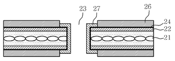
도 4a 내지 4f는 종래기술의 다른 구체예에 따른 인쇄회로기판의 제조과정을 개략적으로 나타낸 공정흐름도이다.Figures 4a to 4f is a process flow diagram schematically showing a manufacturing process of a printed circuit board according to another embodiment of the prior art.
도 5는 종래기술의 일 구체예에 따라 제작된 FCBGA 인쇄회로기판의 구조를 개략적으로 나타낸 단면도이다.5 is a cross-sectional view schematically showing the structure of an FCBGA printed circuit board manufactured according to one embodiment of the prior art.
도 6은 인쇄회로기판용 절연 자재의 유전율 및 손실값 특성을 나타낸 그래프이다.6 is a graph showing dielectric constant and loss value characteristics of an insulating material for a printed circuit board.
도 7은 인쇄회로기판용 절연 자재의 연대별 개발현황을 도식화하여 나타낸 그래프이다.7 is a graph showing the development status by age of the insulation material for printed circuit board.
도 8은 본 발명의 일 구체예에 따라 인쇄회로기판의 제조공정을 개략적으로 나타낸 순서도이다.8 is a flow chart schematically showing a manufacturing process of a printed circuit board according to an embodiment of the present invention.
도 9a 내지 9i는 본 발명의 일 구체예에 따른 인쇄회로기판의 제조과정을 개략적으로 나타낸 공정흐름도이다.9A to 9I are process flowcharts schematically illustrating a manufacturing process of a printed circuit board according to an exemplary embodiment of the present invention.
도 10은 본 발명의 일 구체예에 따른 불소계 수지의 코팅과정을 개략적으로 나타낸 공정흐름도이다. 10 is a process flow diagram schematically showing a coating process of a fluorine-based resin according to an embodiment of the present invention.
도 11은 본 발명의 일 구체예에 따라 제작된 FCBGA 인쇄회로기판의 구조를 개략적으로 나타낸 단면도이다.11 is a schematic cross-sectional view of a structure of an FCBGA printed circuit board manufactured according to an embodiment of the present invention.
※ 도면의 주요 부분에 대한 부호의 설명 ※※ Explanation of code about main part of drawing ※
11 : 수지 절연층 12 : 동박층11: resin insulating layer 12: copper foil layer
13 : 도통홀 14 : 무전해 도금층13: conductive hole 14: electroless plating layer
15 : 구리 패널 도금층 16 : 드라이 필름15 copper
21 : 수지 절연층 22 : 동박층21: resin insulating layer 22: copper foil layer
23 : 도통홀 24 : 무전해 도금층23: through hole 24: electroless plating layer
26 : 드라이 필름 27 : 구리 패턴 도금층26
31 : 제1수지 절연층 32a, 32b : 제1회로층31: first
33 : 도통홀 34a, 34b : 제2수지 절연층33: through
35a, 35b : 제2회로층 36a, 36b : 제3수지 절연층35a, 35b:
37a, 37b : 제3회로층 38a, 38b : 솔더 레지스트층37a, 37b:
101 : 수지 기판 102 : 불소계 수지 코팅층101: resin substrate 102: fluorine-based resin coating layer
103 : 비아홀 104 : 구리 증착층103: via hole 104: copper deposition layer
105 : 드라이 필름 106 : 전해 패턴 도금층105: dry film 106: electrolytic pattern plating layer
107 : 솔더 레지스트층 108 : 솔더 레지스트 오픈부107: solder resist layer 108: solder resist open portion
201, 206, 210 : 수지 기판 202, 207. 211 : 불소계 수지 코팅층201, 206, 210:
203, 208, 212 : 구리 증착층 204, 209, 213 : 전해 패턴 도금층203, 208, 212:
205 : 도통홀 214 : 솔더 레지스트층205: through hole 214: solder resist layer
215 : 솔더 레지스트 오픈부215 solder opening part
본 발명은 인쇄회로기판 및 그 제조방법에 관한 것이다. 좀 더 구체적으로는, 본 발명은 수지 기판에 친수성을 갖는 불소계 수지 코팅층을 형성한 후, 통상의 습식 도금 공정을 건식 도금 공정으로 대체하여 고 신뢰성으로 미세회로 구현이 가능한 인쇄회로기판 및 그 제조방법에 관한 것이다.The present invention relates to a printed circuit board and a method of manufacturing the same. More specifically, the present invention after forming a hydrophilic fluorine-based resin coating layer on the resin substrate, replacing the conventional wet plating process with a dry plating process to realize a fine circuit with high reliability and a manufacturing method thereof It is about.
현재 인쇄회로기판(PCB; Printed Circuit Board)은 서브트렉티브(Subtractive), MSAP(Modified Semi Additive Process) 및 SAP(Semi Additive Process) 공법 등을 이용하여 제작되고 있다.Currently, a printed circuit board (PCB) is manufactured using a subtractive, a modified semi additive process (MSAP), a semi additive process (SAP), and the like.
특히, HDI(High Density Interconnection) 제품은 서브트렉티브 공법을 적용 하며, UT-CSP(Ultra Thin-Chip Scale Package), BGA(Ball Grid Array)는 서브트렉티브 및 MSAP 공법을 적용하며, FCBGA(Flip Chip BGA)는 코어층은 서브트렉티브 공법을, 2F2B/3F3B(build up) 등의 외층은 SAP 공법을 적용하고 있으며, 무전해 도금공정으로 시드층을 형성하여 미세회로를 구현한다.In particular, HDI (High Density Interconnection) products apply the subtractive method, UT-CSP (Ultra Thin-Chip Scale Package), BGA (Ball Grid Array) apply the subtractive and MSAP method, and FCBGA (Flip) Chip BGA) uses the subtractive method for the core layer and the SAP method for the outer layer such as 2F2B / 3F3B (build up), and forms a seed layer by an electroless plating process to implement a microcircuit.
이와 관련하여, 종래기술의 일 구체예에 따라 인쇄회로기판을 제조하는 과정을 도 1에 순서도로 나타내었다.In this regard, a process of manufacturing a printed circuit board according to one embodiment of the prior art is shown in a flow chart in FIG.
도 1을 참조하면, 종래기술의 일 구체예에 따른 인쇄회로기판의 제조방법은 양면 동박적층판 제공 단계(S101), 홀 가공 단계(S102), 디스미어 단계(S103), 무전해 동도금 단계(S104), 전해동 패널 도금 단계(S105), 드라이 필름 도포 단계(S106), 노광/현상 단계(S107), 에칭 단계(S108) 및 드라이 필름 제거 단계(S109)를 포함하여 이루어진다.Referring to Figure 1, the manufacturing method of a printed circuit board according to one embodiment of the prior art is a double-sided copper-clad laminate providing step (S101), hole processing step (S102), desmear step (S103), electroless copper plating step (S104) ), An electrolytic copper panel plating step (S105), a dry film applying step (S106), an exposure / development step (S107), an etching step (S108) and a dry film removal step (S109).
이하, 도 2a 내지 도 2f를 참조하여 본 발명의 일 구체예에 따라 서브트렉티브 공법을 적용하여 인쇄회로기판을 제조하는 과정을 좀 더 구체적으로 설명하면 다음과 같다.Hereinafter, a process of manufacturing a printed circuit board by applying a subtractive method according to an embodiment of the present invention will be described in more detail with reference to FIGS. 2A to 2F.
우선, 수지 절연층(11) 상의 양면에 동박(12)이 적층되어 있는 동박적층판을 통상의 에칭 및 드릴 공정을 통해서 도통홀(13)을 형성한다(도 2a 및 2b 참조). 이어서, 도통홀(13)이 형성된 기판의 표면을 디스미어(desmear) 처리하고 무전해 도금을 통해서 무전해 동박층(14)을 형성한 후(도 2c 참조), 전해 도금을 통해서 Cu 패널 도금층(15)을 형성한다(도 2d 참조). 도통홀(13)을 포함하여 회로패턴이 형성될 소정의 위치에 드라이필름(16)을 도포한 후(도 2e 참조), 통상의 노광/현상 공정을 통해서 불필요한 부분의 동박을 제거한 다음 드라이 필름(16)을 제거하여 패터닝 과정을 완성한다(도 2f 참조).First, the conducting
종래기술의 다른 구체예에 따라 인쇄회로기판을 제조하는 과정을 도 3에 순서도로 나타내었다.According to another embodiment of the prior art, a process of manufacturing a printed circuit board is shown in a flowchart in FIG. 3.
도 3을 참조하면, 종래기술의 다른 구체예에 따른 인쇄회로기판의 제조방법은 양면 동박적층판 제공 단계(S201), 반 에칭 단계(S202), 홀 가공 단계(S203), 디스미어 단계(S204), 무전해 동도금 단계(S205), 드라이 필름 도포 단계(S206), 노광/현상 단계(S207), 전해동 패턴 도금 단계(S208), 드라이 필름 제거 단계(S209) 및 플레시 에칭 단계(S210)을 포함하여 이루어진다.Referring to FIG. 3, a method of manufacturing a printed circuit board according to another exemplary embodiment of the related art includes providing a double-sided copper clad laminate (S201), a semi-etching step (S202), a hole processing step (S203), and a desmear step (S204). Including the electroless copper plating step (S205), dry film coating step (S206), exposure / development step (S207), electrolytic copper pattern plating step (S208), dry film removal step (S209) and flash etching step (S210) Is done.
이하, 도 4a 내지 도 4f를 참조하여 본 발명의 다른 구체예에 따라 MSAP 공법을 적용하여 인쇄회로기판을 제조하는 과정을 좀 더 구체적으로 설명하면 다음과 같다.Hereinafter, a process of manufacturing a printed circuit board by applying the MSAP method according to another embodiment of the present invention will be described in more detail with reference to FIGS. 4A to 4F.
우선, 수지 절연층(21) 상의 양면에 동박(22)이 적층되어 있는 동박적층판을 반-에칭(Half-etching)한 후(도 4a 참조), 통상의 에칭 및 드릴 공정을 통해서 도통홀(23)을 형성한다(도 4b 참조). 이어서, 도통홀(23)이 형성된 기판의 표면을 디스미어 처리하고 무전해 도금을 통해서 무전해 동박층(24)을 형성한 후(도 4c 참조), 도통홀(23)을 포함하여 회로패턴이 형성될 위치를 제외한 소정의 위치에 드라이필름(26)을 도포한 후(도 4d 참조), 이를 레지스로 하여 전해 도금을 통해서 Cu 패턴 도금층(27)을 형성한다(도 4e 참조). 다음, 드라이 필름(26)을 제거하고 플레시 에칭을 통해서 불필요한 부분의 동박층을 제거하여 패터닝 과정을 완성한다 (도 4f 참조).First, after the half-etching of the copper-clad laminate in which the
한편, 각 제품별 기존 수지 절연층 자재로는 통상적으로 FR-4, BT(BismaleimideTriazine), ABF(Ajinomoto Build up Film) 등의 에폭시계 수지가 사용되고 있는데, 고 유전율(Dk>3.5[ABF]∼4.5[BT, FR-4]), 고 손실계수(Df>0.05)로 인하여 신호전송속도 및 전송손실로 열발생 및 전기적인 특성이 저하되는 단점이 있다.On the other hand, epoxy resins such as FR-4, BT (BismaleimideTriazine) and ABF (Ajinomoto Build up Film) are commonly used as the existing resin insulating layer materials for each product, and have a high dielectric constant (Dk> 3.5 [ABF] to 4.5). [BT, FR-4]) and the high loss factor (Df> 0.05) have the disadvantage of deteriorating heat generation and electrical characteristics due to signal transmission speed and transmission loss.
예를 들어, BT 절연 자재를 사용하여 서브트렉티브 및 MSAP 공법을 적용하고 있는 BGA, UT-CSP 제품의 경우, 원자재의 표면 프로파일이 1㎛ 이상이며, 서브트렉티브 공법에서는 L/S(Line/Space)=50/50㎛이 최소의 회로폭 한계로 알려져 있고, MSAP 공법에서 역시 반-에칭(Half etching)을 하기 때문에 Cu층에 두께 편차가 발생되어 L/S=25/25㎛가 최소의 회로폭 한계인 것으로 알려져 있는 바, 피치가 50㎛(L/S=25/25㎛) 이하인 미세회로 구현에는 한계가 있다.For example, for BGA and UT-CSP products using the BT insulating material using the subtractive and MSAP methods, the surface profile of the raw material is 1 µm or more, and in the subtractive method, L / S (Line / Space) = 50 / 50㎛ is known as the minimum circuit width limit, and because the half etching is also performed in the MSAP method, thickness variation occurs in the Cu layer, and L / S = 25 / 25㎛ is the minimum. It is known that the circuit width limit is limited in the implementation of the microcircuit having a pitch of 50 μm or less (L / S = 25/25 μm).
한편, FCBGA 제품군에서는 ABF 절연 자재를 사용하며, 다층기판을 SAP 공법으로 제작하고 있다. 즉, 도 5에 나타낸 바와 같이, 코어층(1층∼2층)은 서브트렉티브 공법을 적용하고, 외층(3층∼6층)은 SAP 공법을 적용하여 무전해 도금 공정으로 1∼3㎛ 정도의 도금 두께를 형성하며 회로공정을 거쳐 도금, 박리, 플레시 에칭 공정을 2회 반복하여 각 수지 절연층(31, 34a, 34b, 36a, 36b)에 도통홀(33)을 비롯하여 회로패턴(32a, 32b, 35a, 35b, 37a, 37b)을 형성한 후, 솔더 레지스트(38a, 38b)를 도포하고 솔더 레지스트 오픈부(39a, 39b)를 형성하여 총 6층의 FCBGA 기판을 제작한다.Meanwhile, the FCBGA product family uses ABF insulation materials and manufactures multilayer boards using the SAP method. That is, as shown in Fig. 5, the core layers (1 to 2 layers) apply the subtractive method, and the outer layers (3 to 6 layers) apply the SAP method to 1 to 3 mu m in an electroless plating process. Forming a plating thickness of about a degree, and repeating the plating, peeling, and flash etching process twice through the circuit process, including the
그러나, 고가의 ABF 원자재를 사용함에 따라 공정단가의 상승으로 인하여 생산단가가 높으며, 상술한 SAP 공법을 적용하는 경우 ABF 원자재의 표면 프로파일이 1㎛ 이상으로 표면조도가 크고 피치(Line/Space)가 18/18㎛이며, 습식 표면처리 및 무전해 화학도금을 통하여 미세회로 공법을 구현하는데 있어서 한계가 있었다.However, the production cost is high due to the increase of the process cost due to the use of expensive ABF raw materials, and the surface profile of the ABF raw materials is 1 µm or more and the surface roughness is large and the pitch (Line / Space) is high when the above-described SAP method is applied. 18 / 18㎛, there was a limit in implementing the microcircuit method through the wet surface treatment and electroless chemical plating.
점차적으로 인쇄회로기판은 경박 단소화로 인하여 미세회로 구현 및 고기능 절연 자재를 사용하여 회로상의 신호전송속도를 향상시키려고 각 업체별로 개발 진행중이다. 현 개발 방향에 맞추어 신호 입력/출력이 증가하므로 미세회로 구현이 필요하며, 이에 따라 고기능 절연 자재인 PTFE(Poly Tetra Fluoro Ethylene), PI(Polyimide), LCP(Liquid Crystal Polymer), 본딩 시트(Bonding Sheet), TPI(Thermal Plastic Polyimide) 등 저유전율 및 저손실계수의 특성을 가진 절연 자재를 이용하여 신호전송속도를 향상시키고 있는 추세이다. 또한, 원자재의 표면 프로파일에 0.5㎛ 이하의 조도를 형성하여 SAP 공법으로 미세회로 형성이 가능하도록 한다. 그러나, 종래의 SAP 공법은 습식 표면처리 및 무전해 도금을 적용한 습식 공정을 통해서 Cu층을 형성함으로써 표면조도가 커져 미세회로의 구현에 한계가 있을 뿐 아니라, 폐기물이 다량 발생되어 환경 친화적이지 못한 단점이 있다.Increasingly, printed circuit boards are being developed by each company in order to improve the signal transmission speed on the circuit by implementing microcircuits and using high-performance insulating materials due to light and thin shortening. As the signal input / output increases according to the current development direction, it is necessary to implement a microcircuit. Accordingly, PTFE (Poly Tetra Fluoro Ethylene), PI (Polyimide), LCP (Liquid Crystal Polymer), and Bonding Sheet are required. ), It is a trend to improve the signal transmission speed by using insulating materials with low dielectric constant and low loss factor such as TPI (Thermal Plastic Polyimide). In addition, by forming a roughness of 0.5㎛ or less on the surface profile of the raw material to enable the formation of microcircuits by the SAP method. However, the conventional SAP method has a limitation in realizing microcircuits due to surface roughness by forming a Cu layer through a wet process using wet surface treatment and electroless plating, and a large amount of waste, which is not environmentally friendly. There is this.
이에 본 발명에서는 상기와 같은 문제점을 해결하기 위하여 광범위한 연구를 거듭한 결과, 수지 기판에 친수성을 갖는 불소계 수지 코팅층을 형성한 후, 건식 공정을 통해서 구리층을 형성함으로써 고 신뢰성으로 미세회로의 구현이 가능한 인 쇄회로기판을 얻을 수 있었고, 본 발명은 이에 기초하여 완성되었다.Accordingly, in the present invention, as a result of extensive research to solve the above problems, after forming a hydrophilic fluorine-based resin coating layer on the resin substrate, by forming a copper layer through a dry process, it is possible to implement a microcircuit with high reliability. Possible printed circuit boards have been obtained, and the present invention has been completed based on this.
따라서, 본 발명의 목적은 표면조도의 변화없이 수지 기판의 계면 밀착력을 향상시켜 고 신뢰성으로 미세회로를 구현할 수 있는 인쇄회로기판 및 그 제조방법을 제공하는데 있다.Accordingly, an object of the present invention is to provide a printed circuit board and a method of manufacturing the same, which can implement a fine circuit with high reliability by improving the interfacial adhesion of the resin substrate without changing the surface roughness.
본 발명의 다른 목적은 저 유전율과 낮은 손실계수 특성을 갖는 인쇄회로기판 및 그 제조방법을 제공하는데 있다.Another object of the present invention is to provide a printed circuit board having a low dielectric constant and a low loss factor and a method of manufacturing the same.
본 발명의 또 다른 목적은 통상의 습식 동도금층 형성공정을 건식공정으로 대체함으로써 친환경적으로 제작이 가능한 인쇄회로기판 및 그 제조방법을 제공하는데 있다.Still another object of the present invention is to provide a printed circuit board and a method of manufacturing the same, which can be manufactured in an environmentally friendly manner by replacing the conventional wet copper plating layer forming process with a dry process.
본 발명의 일 면에 따르면, According to one aspect of the invention,
(a) 인쇄회로기판용 수지 기판을 제공하는 단계; (a) providing a resin substrate for a printed circuit board;
(b) 상기 수지 기판의 적어도 일면에 불소계 수지를 코팅하는 단계; (b) coating a fluorine resin on at least one surface of the resin substrate;
(c) 상기 불소계 수지가 코팅된 기판에 층간 전기적 도통을 위한 적어도 하나의 비아홀을 형성하는 단계; (c) forming at least one via hole for interlayer electrical conduction on the fluorine resin coated substrate;
(d) 상기 비아홀이 형성된 기판의 표면을 이온빔을 이용하여 표면처리하는 단계; (d) surface treating the surface of the substrate on which the via hole is formed using an ion beam;
(e) 상기 표면처리된 기판 상에 진공 증착법을 이용하여 구리 시드층을 형성하는 단계; (e) forming a copper seed layer on the surface treated substrate using vacuum deposition;
(f) 상기 구리 시드층이 형성된 기판을 구리 패턴 도금하는 단계; 및(f) copper pattern plating the substrate on which the copper seed layer is formed; And
(g) 상기 구리 패턴 도금층이 형성되지 않은 부위의 구리 시드층을 제거하는 단계;(g) removing the copper seed layer at the portion where the copper pattern plating layer is not formed;
를 포함하는 것을 특징으로 하는 인쇄회로기판의 제조방법이 제공된다.Provided is a method of manufacturing a printed circuit board comprising a.
여기서, 상기 불소계 수지는 PTFE(Poly Tetra Fluoro Ethylene), PI(Polyimide), LCP(Liquid Crystal Polymer), TPI(Thermal Plastic Polyimide), FEP(Fluorinated Ethylene Propylene), PFA(Perfluoroalkoxy), ETFE(Ethylene-Tetra Fluoro Ethylene), PVDF(PolyVinyliDen Fluoride), ECTFE(EthyleneChlorotriFluoroEthylene), PCTFE(PolyChloroTriFluoroEthylene) 및 이들의 조합으로 이루어진 군으로부터 선택될 수 있다.Here, the fluorine-based resin is PTFE (Poly Tetra Fluoro Ethylene), PI (Polyimide), LCP (Liquid Crystal Polymer), TPI (Thermal Plastic Polyimide), FEP (Fluorinated Ethylene Propylene), PFA (Perfluoroalkoxy), ETFE (Ethylene-Tetra) Fluoro Ethylene (PVDF), PolyVinyliDen Fluoride (PVDF), EthyleneChlorotriFluoroEthylene (ECTFE), PolyChloroTriFluoroEthylene (PCTFE), and combinations thereof.
바람직하게는, 상기 불소계 수지 코팅 단계가 기판 상에 액상의 불소계 수지를 도포한 후, 100∼450℃의 온도에서 열처리하여 수행될 수 있다. 이때, 상기 불소계 수지 도포 및 열처리 과정은 1∼10회 반복하여 수행될 수 있다. 한편, 상기 불소계 수지 코팅 단계는 시트 타입(sheet type) 또는 롤-투-롤 타입(roll-to-roll type)으로 수행될 수 있다.Preferably, the fluorine-based resin coating step may be performed by applying a liquid fluorine-based resin on the substrate, and then heat treatment at a temperature of 100 ~ 450 ℃. In this case, the fluorine-based resin coating and heat treatment process may be performed repeatedly 1 to 10 times. On the other hand, the fluorine-based resin coating step may be performed in a sheet type (roll type) or a roll-to-roll type (roll-to-roll type).
바람직하게는, 상기 이온빔 표면처리 단계가 Ar, O2, N2, Xe, CF4, H2, Ne, Kr 및 이들의 혼합 가스로 이루어진 군으로부터 선택되는 불활성 가스의 존재하에서 수행될 수 있다.Preferably, the ion beam surface treatment step may be performed in the presence of an inert gas selected from the group consisting of Ar, O 2 , N 2 , Xe, CF 4 , H 2 , Ne, Kr and mixtures thereof.
바람직하게는, 상기 진공 증착법이 스퍼터(sputter), 열증착(thermal evaporation) 또는 이-빔(e-beam)법일 수 있다.Preferably, the vacuum deposition method may be a sputter, thermal evaporation, or e-beam method.
한편, 상기 불소계 수지의 코팅 두께가 20nm∼10㎛이고, 상기 구리 시드층의 두께가 20nm∼4㎛인 것이 바람직하다.On the other hand, it is preferable that the coating thickness of the said fluorine resin is 20 nm-10 micrometers, and the thickness of the said copper seed layer is 20 nm-4 micrometers.
상기 수지 기판은 에폭시계 수지 또는 불소계 수지로 된 기판일 수 있다.The resin substrate may be a substrate made of epoxy resin or fluorine resin.
본 발명의 다른 일면에 따르면,According to another aspect of the present invention,
(a) 인쇄회로기판용 수지 기판; (a) a resin substrate for a printed circuit board;
(b) 상기 수지 기판의 적어도 일면에 형성되는 불소계 수지 코팅층; (b) a fluorine resin coating layer formed on at least one surface of the resin substrate;
(c) 상기 불소계 수지가 코팅된 기판의 소정 위치에 형성되는 비아홀; (c) via holes formed at predetermined positions of the substrate coated with the fluorine resin;
(d) 상기 비아홀이 형성된 기판의 표면에 이온빔 표면처리 및 진공 증착법을 통해서 형성되는 구리 시드층; 및(d) a copper seed layer formed on the surface of the substrate on which the via holes are formed by ion beam surface treatment and vacuum deposition; And
(e) 상기 구리 시드층이 형성된 기판상의 소정 부위 및 비아홀에 형성되는 구리 패턴 도금층; (e) a copper pattern plating layer formed on predetermined portions and via holes on the substrate on which the copper seed layer is formed;
을 포함하는 것을 특징으로 하는 인쇄회로기판이 제공된다.There is provided a printed circuit board comprising a.
이하, 본 발명을 첨부된 도면을 참조하여 좀 더 구체적으로 살펴보면 다음과 같다.Hereinafter, the present invention will be described in more detail with reference to the accompanying drawings.
전술한 바와 같이, 본 발명에 따르면, 인쇄회로기판 제작시 기존의 습식 공정인 표면조도 형성 공정과 무전해 도금 공정을 건식 공정으로 대체하여 친환경적으로 표면조도의 프로파일 없이 밀착력을 확보하여 미세회로를 구현할 수 있다.As described above, according to the present invention, by replacing the conventional wet surface roughness forming process and the electroless plating process with a dry process when manufacturing a printed circuit board, it is possible to implement microcircuits by securing adhesion without environmentally rough surface profile. Can be.
참고를 위하여, 통상의 인쇄회로기판용 수지 기판으로서 사용되는 절연 자재 의 유전율 및 손실값 특성과, 연대별 개발현황을 도 6 및 도 7에 각각 나타내었다. 또한, 하기 표 1에 절연 자재 별 유전율과 전파 지연 속도 특성을 정리하여 나타내었다.For reference, the dielectric constant and loss value characteristics of the insulating material used as a conventional resin substrate for a printed circuit board, and the development status by age are shown in FIGS. 6 and 7, respectively. In addition, Table 1 shows the dielectric constant and propagation delay rate characteristics for each insulating material.
상기에서 살펴본 바와 같이, 종래에는 서브트렉티브 & MSAP 공법의 미세회로 구현의 한계로 인하여, SAP 공법으로 미세회로 구현을 하고 있으나 절연 자재의 높은 표면조도 프로파일(즉, >1㎛)로 미세회로 구현에 한계점이 있었다. 또한, 기존의 SAP 공법에서는 절연 자재와 무전해 도금층과의 밀착력을 확보하기 위하여 절연재에 예를 들어, 디스미어 처리, 즉, 과망간산으로 스미어를 제거하고 표면에 조도를 형성하며, 잔류 이산화망간을 제거하는 중화 공정[CH4 + 12MnO4 - +14OH- → CO3 2 - + 12MnO4 2 - + 9H20 + O2])을 수행하는 것과 같은 습식 표면조도 공정을 통해서 표면조도를 형성하고 무전해 도금을 하여 Cu 시드층을 형성하는 등의 습식 공정으로 인하여 폐액 발생 및 환경적으로 문제점이 있었다.As described above, due to the limitation of the microcircuit implementation of the subtractive & MSAP method, the microcircuit is implemented by the SAP method, but the microcircuit is realized by the high surface roughness profile (ie,> 1 μm) of the insulating material. There was a limitation. In addition, in the existing SAP method, in order to secure adhesion between the insulating material and the electroless plating layer, for example, desmear treatment, that is, desmearing with permanganic acid, roughness is formed on the surface, and residual manganese dioxide is removed. neutralization [CH 4 + 12MnO 4 - + 14OH - →
이에 반하여, 본 발명에서는 습식 표면조도 형성 공정을 건식 이온빔 표면처리 공정으로 대체하는 동시에, 무전해 도금 공정을 진공 증착 공정으로 대체함으로써 환경친화적인 공정을 통해서 최소한의 표면조도 (Ra<0.5㎛)로 미세회로 구현이 가능하다.In contrast, in the present invention, the wet surface roughness forming process is replaced by a dry ion beam surface treatment process, and the electroless plating process is replaced by a vacuum deposition process to minimize surface roughness (Ra <0.5 μm) through an environmentally friendly process. It is possible to implement a fine circuit.
본 발명의 바람직한 일 구체예에 따라 인쇄회로기판을 제조하는 과정을 도 8에 순서도로 나타내었다.8 is a flow chart illustrating a process of manufacturing a printed circuit board according to an exemplary embodiment of the present invention.
도 8을 참조하면, 본 발명의 바람직한 일 구체예에 따른 인쇄회로기판의 제조방법은 수지 기판 제공 단계(S1001), 불소계 수지 코팅 단계(S1002), 홀 가공 단계(S1003), 이온빔 표면처리 단계(S1004), 구리층 진공증착 단계(S1005), 드라이 필름 도포 단계(S1006), 노광/현상 단계(S1007), 전해 패턴 도금 단계(S1008), 드라이 필름 제거 단계(S1009) 및 플레시 에칭 단계(S1010)를 포함하여 이루어진다.Referring to Figure 8, the manufacturing method of the printed circuit board according to an embodiment of the present invention is a resin substrate providing step (S1001), fluorine-based resin coating step (S1002), hole processing step (S1003), ion beam surface treatment step ( S1004), copper layer vacuum deposition step (S1005), dry film coating step (S1006), exposure / development step (S1007), electrolytic pattern plating step (S1008), dry film removal step (S1009) and flash etching step (S1010) It is made, including.
이하, 도 9a 내지 도 9i를 참조하여 본 발명의 바람직한 일 구체예에 따라 인쇄회로기판을 제조하는 과정을 좀 더 구체적으로 설명한다.Hereinafter, a process of manufacturing a printed circuit board according to an exemplary embodiment of the present invention will be described in more detail with reference to FIGS. 9A to 9I.
우선, 당업계에서 사용되는 통상의 에폭시계 수지 또는 불소계 수지로 된 인쇄회로기판용 수지 기판(101)을 준비한다(도 9a 참조).First, a
이어서, 상기 수지 기판(101)의 적어도 일면에 액상 불소계 수지를 이용하여 불소계 수지 코팅층(102)을 형성시킨다(도 9b 참조).Subsequently, a fluorine
기존의 FR-4, BT, ABF 등의 에폭시계 수지로 된 기판 원자재는 불소계 수지 원자재와 달리 이온빔 표면처리 효과가 떨어지는 단점이 있는 바, 이를 개선하기 위하여 본 발명에서는 에폭시계 원자재의 표면에 액상의 불소계 수지를 도포 및 열처리하여 표면의 형상을 불소계 수지 형태로 변화시키고 고분자 표면에 이온빔을 이용한 표면처리로 자재 계면 밀착력을 강화시키는 기술을 적용한다. 즉, 고분자 표면에 에너지를 가진 불활성 또는 반응성 이온을 조사(照射)하여 여기시켜 불안정한 고리를 형성시키고 반응 가스를 공급함으로써 화학반응을 일으켜 고분자 표면에 친수성 작용기를 형성시킴으로써 소수성에서 친수성 특성을 가지는 물질로 변화시켜 이온빔 표면처리 효과를 향상시킬 수 있다. 뿐만 아니라, 이온빔 표면처리 효과가 떨어지는 일부 불소계 수지로 된 기판 원자재도 이온빔 처리효과가 잘 나타나는 불소계 수지 물질을 표면에 코팅하여 원하는 특성의 물질을 가진 절연 자재를 만들 수 있다.Unlike conventional fluorine resin raw materials, substrate raw materials made of epoxy resins such as FR-4, BT, and ABF have a disadvantage in that the ion beam surface treatment effect is inferior. By applying and heat-treating fluorine-based resin, the shape of the surface is changed to fluorine-based resin and the surface treatment using ion beam is applied to the surface of polymer to strengthen the material interface adhesion. In other words, by irradiating and energizing inert or reactive ions with energy on the surface of the polymer to form an unstable ring and supplying a reaction gas, a chemical reaction occurs to form a hydrophilic functional group on the surface of the polymer to form a hydrophobic to hydrophilic material. It can be changed to improve the ion beam surface treatment effect. In addition, a substrate material made of some fluorine-based resins having a low ion beam surface treatment effect may be coated on a surface of a fluorine-based resin material exhibiting an ion beam treatment effect to form an insulating material having a material having desired properties.
본 발명에서 사용되는 불소계 수지로는, 바람직하게는, PTFE(Poly Tetra Fluoro Ethylene), PI(Polyimide), LCP(Liquid Crystal Polymer), TPI(Thermal Plastic Polyimide), PFA(Perfluoroalkoxy), FEP(Fluorinated Ethylene Propylene), ETFE(Ethylene-Tetra Fluoro Ethylene), PVDF(PolyVinyliDen Fluoride), ECTFE(Ethylene-ChlorotriFluoroEthylene), PCTFE(PolyChloroTriFluoroEthylene) 중에서 단독 또는 2 이상이 선택될 수 있으나, 특별히 이에 한정되는 것은 아니다.As the fluorine resin used in the present invention, Preferably, PTFE (Poly Tetra Fluoro Ethylene), PI (Polyimide), LCP (Liquid Crystal Polymer), TPI (Thermal Plastic Polyimide), PFA (Perfluoroalkoxy), FEP (Fluorinated Ethylene) Propylene), ETFE (Ethylene-Tetra Fluoro Ethylene), PVDF (PolyVinyliDen Fluoride), ECTFE (Ethylene-ChlorotriFluoroEthylene), PCTFE (PolyChloroTriFluoroEthylene) may be selected alone or two or more, but is not particularly limited thereto.
이러한 액상의 불소계 수지를 이용하여 수지 기판(101) 상에 불소계 수지 코팅층(102)을 형성하는 과정의 바람직한 구체예를 도 10을 참조하여 설명하면 다음과 같으나, 당업계에 공지된 것이라면 특별히 이에 한정되는 것은 아님이 주지되어야 한다.The preferred embodiment of the process of forming the fluorine-based
롤-투-롤 타입(roll-to-roll type)의 기판 절연 자재를 적용하는 경우(도 10의 좌측 참조)에는 함침기를 이용하여 액상 불소계 수지가 담긴 함침욕(bath)을 통과시킨 후 열처리 공정에서 단면 및 양면에 불소계 수지를 도포한 원자재를 사용된 불소계 수지에 맞는 온도로 열처리하여 경화시키며, 시트 타입(sheet type)의 절연 자재를 적용하는 경우(도 10의 우측)에는 스크린 타입 및 롤러를 이용하여 기판 절연 자재 위에 액상 불소계 수지를 도포한 후 열처리 공정을 거쳐 경화시킨다.In case of applying a roll-to-roll type substrate insulating material (see left side of FIG. 10), a heat treatment process is performed after passing an impregnation bath containing a liquid fluorine resin using an impregnator. The raw material coated with fluorine resin on one side and both sides is cured by heat treatment at a temperature suitable for the used fluorine resin, and when a sheet type insulating material is applied (right side of FIG. 10), a screen type and a roller are used. The liquid fluorine resin is applied onto the substrate insulating material, and then cured through a heat treatment step.
특히, 롤-투-롤 타입은 롤에 원자재 샘플을 로딩하고 욕(Bath)에는 원하는 액상 불소계 수지를 넣고 적당한 온도 및 습도를 조절하여 욕에서 불소계 수지를 도포한다. 다음, 타워에서 열처리 과정을 통해서 수지 흐름(Resin flow)을 조절하여 함침을 반복적으로 1회∼10회로 조절하여 원하는 절연 자재의 두께, 유전율 및 손실계수를 얻을 수 있다.In particular, the roll-to-roll type loads a raw material sample onto a roll, puts a desired liquid fluorine-based resin in a bath, and applies a fluorine-based resin in a bath by adjusting an appropriate temperature and humidity. Next, by adjusting the resin flow through heat treatment in the tower, the impregnation may be repeatedly adjusted once to 10 times to obtain a desired thickness, dielectric constant, and loss factor of the insulating material.
이와 같은 도포/열처리 과정을 통해서 수지 기판의 단면/양면에 선택적으로 불소계 수지를 함침시킬 수 있다. 즉, 단면만을 함침시키는 경우에는 원자재의 일면에 이형 필름(Release film; PET, PPE film 등)을 부착하여 코팅 공정 후에 이형 필름을 제거하여 일면에만 원하는 불소계 수지를 코팅할 수 있고, 양면일 경우에는 원자재를 함침기에 디핑하여 원하는 두께만큼 수지 흐름을 조절할 수 있다. 이와 같은 과정을 통해서 저 유전율 및 낮은 손실계수의 특성을 발현시킬 수 있으며, 이로부터 얻은 기판은 적용목적에 따라 적층용으로 사용될 수도 있다.Through such an application / heat treatment process, the fluorine-based resin can be impregnated selectively on the cross-section / both surfaces of the resin substrate. That is, in the case of impregnating only one side surface, a release film (Release film; PET, PPE film, etc.) may be attached to one surface of the raw material to remove the release film after the coating process to coat the desired fluorine resin on only one surface. Raw material can be dipped into the impregnator to control the resin flow to the desired thickness. Through this process, it is possible to express the characteristics of low dielectric constant and low loss factor, and the substrate obtained therefrom may be used for lamination depending on the application purpose.
또한, 시트 타입은 구체적으로는 시트에 원자재 샘플을 로딩하고 스크린 프린팅으로 스퀴지 및 롤러로 원하는 액상 불소계 수지를 밀어 넣고 적당한 온도 및 습도를 조절하여 욕(bath)에서 불소계 수지를 도포하고 열처리하여 수지의 흐름을 조절하고 함침 과정을 반복적으로 1회∼10회 수행하여 원하는 절연 자재의 두께, 저 유전율 및 낮은 손실계수를 얻을 수 있다.In addition, the sheet type specifically loads a raw material sample on the sheet, pushes the desired liquid fluorine resin with a squeegee and a roller by screen printing, and adjusts an appropriate temperature and humidity to apply a fluorine resin in a bath and heat-treat the resin. By controlling the flow and repeating the impregnation process one to ten times, the desired insulation material thickness, low dielectric constant and low loss factor can be obtained.
여기서, 상기 불소계 수지 코팅 공정은 수지 기판의 유전율 및 손실계수와 두께를 조절하기 위하여 도포 및 열처리 과정을 1∼10회 반복 진행하여 원하는 절연 자재의 특성을 얻는다. 상기 열처리 온도는 불소계 수지의 종류에 따라 다르나, 통상 액상의 불소계 수지가 경화되는 온도는 100℃∼450℃인 것이 전형적이다.Here, the fluorine-based resin coating process is repeated 1 to 10 times the coating and heat treatment process in order to adjust the dielectric constant, loss coefficient and thickness of the resin substrate to obtain the characteristics of the insulating material. The heat treatment temperature varies depending on the type of fluorine resin, but the temperature at which the liquid fluorine resin is cured is typically 100 ° C to 450 ° C.
구체적으로는, 상기 불소계 수지 코팅 공정 조건은, PI는 300∼420℃, PTFE는 350∼420℃, LCP는 250∼420℃, TPI는 250∼350℃, 본딩 시트(Bonding sheet)는 150∼250℃, 습도는 <RH 50%, 코팅층 두께는 코팅의 회수를 많이 할수록 유전율이 낮아지므로 주파수 특성이 좋아지나 경제성 대비 효율성을 감안하여 1∼10회가 적당하다.Specifically, the fluorine-based resin coating process conditions, PI is 300 ~ 420 ℃, PTFE is 350 ~ 420 ℃, LCP 250 ~ 420 ℃, TPI 250 ~ 350 ℃, bonding sheet (Bonding sheet) 150 ~ 250 ℃, humidity <
이로부터 형성되는 불소계 수지의 코팅 두께는 절연 자재 및 이에 코팅되는 불소계 수지의 종류에 따라 적절하게 조절될 수 있으며 20nm∼10㎛인 것이 바람직하다. 즉, 유리 직물(Glass cloth)의 유전율은 약 6.2이며 에폭시, BT 수지의 유전율은 약 3.5로서, 원자재의 강도를 유지하기 위하여 인쇄회로기판은 유리 직물에 예를 들어, 에폭시, BT 수지를 1∼5회 정도 코팅하여 유전율을 4.5 정도로 조절하여 사용하고 있으며 함침을 많이 할수록 유전율이 떨어지게 된다.The coating thickness of the fluorine-based resin formed therefrom may be appropriately adjusted according to the type of insulating material and the fluorine-based resin coated thereon, and is preferably 20 nm to 10 μm. That is, the dielectric constant of glass cloth is about 6.2, and the dielectric constant of epoxy and BT resin is about 3.5. In order to maintain the strength of raw materials, the printed circuit board is made of glass cloth, e.g. 5 times coating is used to adjust the dielectric constant to about 4.5 and the more the impregnation, the lower the dielectric constant.
일례로서, 유리 직물(유전율 6.2)에 PTFE(유전율 2.1)를 함침공정을 거치면 유전율을 2.2∼4.0까지 조절할 수 있으며 코팅 회수를 많이 할수록 유전율 및 손실계수를 낮출 수 있으며 원하는 유전율 및 손실계수를 얻을 수 있다. 이와 같은 방법으로 유리 직물, BT, 에폭시에 PTFE, PI, LCP, TPI, PFA, FEP, ETFE, ECTFE 등을 함침 및 코팅하면 유전율 및 손실계수를 낮출 수 있으며 1∼10회를 반복하면 원하는 두께와 유전율 및 손실계수를 얻을 수 있다.For example, the glass dielectric material (dielectric constant 6.2) is impregnated with PTFE (dielectric constant 2.1) to control the dielectric constant from 2.2 to 4.0. The more coatings, the lower the dielectric constant and loss coefficient, and the desired dielectric constant and loss coefficient can be obtained. have. In this way, impregnating and coating glass fabric, BT, epoxy with PTFE, PI, LCP, TPI, PFA, FEP, ETFE, ECTFE, etc., can lower the dielectric constant and loss factor. The permittivity and loss factor can be obtained.
다음, 상기 불소계 수지 코팅층(102)이 형성된 기판에 층간 전기적 도통을 위한 적어도 하나의 비아홀용 도통홀(103)을 형성한 후(도 9c 참조), 상기 비아홀(103)이 형성된 기판의 표면을 이온빔을 이용하여 표면처리한다.Next, after the at least one via hole through
바람직하게는, 상기 이온빔 표면처리 과정은 Ar, O2, N2, Xe, CF4, H2, Ne, Kr 및 이들의 혼합 가스로 이루어진 군으로부터 선택되는 불활성 가스의 존재하에서 1E15∼1E19(ions/㎠)의 이온주입량으로 수행될 수 있으나, 특별히 이에 한정되는 것은 아니다. 보다 구체적으로는, 이온주입량은 재료에 따라 다르나, 통상적으로 PI, PTFE, LCP, TPI, 본딩 시트,불소계 수지는 가속전압이 0.5∼20KeV, 이온주입량이 1E15~1E19 ion dose/㎠인 것이 적당하다.Preferably, the ion beam surface treatment is performed in the presence of an inert gas selected from the group consisting of Ar, O 2 , N 2 , Xe, CF 4 , H 2 , Ne, Kr and mixtures thereof. / Cm 2) may be performed with an ion implantation amount, but is not particularly limited thereto. More specifically, the amount of ion implantation varies depending on the material, but in general, PI, PTFE, LCP, TPI, bonding sheets, and fluorine-based resins preferably have an acceleration voltage of 0.5 to 20 KeV and an ion implantation amount of 1E15 to 1E19 ion dose /
이와 같은 건식 이온빔 표면처리 과정을 통해서 수지 기판과 후속 과정에서 생성될 Cu 시드층과의 밀착력을 확보할 수 있다. 즉, 고분자 표면에 에너지를 가진 불활성 또는 반응성 이온을 조사하여 여기시켜 불안정한 고리를 형성하여 반응 가스인 산소를 공급함으로써 화학반응을 일으켜 고분자 표면에 친수성 작용기를 형성하여 표면조도의 변화없이(Ra<0.5㎛) 자재 계면 밀착력을 강화시켜 미세회로 구현이 가능한 것이다.Through such a dry ion beam surface treatment, adhesion between the resin substrate and the Cu seed layer to be generated in a subsequent process can be ensured. In other words, by irradiating and energizing inert or reactive ions with energy on the surface of the polymer to form an unstable ring to supply oxygen as a reaction gas to cause a chemical reaction to form a hydrophilic functional group on the surface of the polymer without changing the surface roughness (Ra <0.5 Μm) It is possible to realize a fine circuit by strengthening the adhesion of the material interface.
이어서, 상기 이온빔 표면처리된 기판 상에 진공 증착법을 이용하여 원하는 두께의 구리 시드층(104)을 형성시킨다(도 9d 참조).Subsequently, a
상기 진공 증착법은, 바람직하게는, 스퍼터(sputter), 열증착(thermal evaporation) 또는 이-빔(e-beam)법일 수 있으나, 당업계에 공지된 것이라면 특별히 이에 한정되는 것은 아니다.The vacuum deposition method may be, preferably, a sputter, thermal evaporation, or e-beam method, but is not particularly limited as long as it is known in the art.
이로부터 형성되는 구리 시드층의 두께는 20nm∼4㎛인 것이 바람직하다. 참고로, 기존 CZ 처리와 무전해 도금 공정에서는 <3㎛ 두께의 Cu를 형성하고 SAP(Semi Additive Process) 공법을 진행한다.It is preferable that the thickness of the copper seed layer formed from this is 20 nm-4 micrometers. For reference, in the existing CZ treatment and the electroless plating process, Cu having a thickness of <3 μm is formed and a SAP (Semi Additive Process) method is performed.
이와 같이, 기존의 구리 시드층 형성 공정인 무전해 도금방법을 진공 증착법으로 대체함으로써 습식 공정을 건식 공정으로 전환하여 폐액 등이 발생되지 않으므로 친환경적이다.As such, by replacing the conventional electroless plating method, which is a copper seed layer forming process, with a vacuum deposition method, the wet process is converted into a dry process, and waste liquids are not generated.
다음, 당업계에 공지된 바에 따라, 패턴 도금할 부분을 제외한 소정의 부위에 도금 레지스트로 작용할 드라이 필름(105)을 도포하고(도 9e 참조), 구리 패턴 도금한 후 드라이 필름(105)을 제거하여 패턴 도금층(106)을 형성시킨다(도 9f 참조).Next, as known in the art, apply a
한편, 패턴 도금층(106)이 형성되지 않은 부위의 구리 시드층(104)은 통상의 플레시 에칭법을 이용하여 제거한다(도 9g 참조).On the other hand, the
이와 같이 패턴 도금된 인쇄회로기판은 적용 목적에 따라 통상의 적층 및 회로 패턴 형성 과정이 반복적으로 수행되어 다층용 인쇄회로기판으로서 사용될 수 있다.The pattern plated printed circuit board may be used as a multilayer printed circuit board by performing a conventional lamination and circuit pattern forming process repeatedly according to an application purpose.
또한, 선택적으로는, 최외각층용으로 적용될 경우에 한해서, 당업계에 공지된 바에 따라, 솔더 레지스트(107)를 도포하고 통상의 솔더 레지스트 오픈 공정을 통해서 솔더 레지스트 오픈부(108)를 형성할 수 있다(도 9h 및 9i 참조).Also, optionally, only when applied for the outermost layer, the solder resist
상술한 공정에 따라 형성된 6층 FCBGA 기판의 일례를 도 11에 나타내었다.An example of the six-layer FCBGA substrate formed in accordance with the above-described process is shown in FIG.
도 11을 참조하면, 코어층으로서 양면에 불소계 수지 코팅층(202)이 형성된 제1의 수지 기판(201)에 구리 증착층(203)과 전해 패턴 도금층(204)를 포함하는 제1회로층과 비아홀(205)이 형성되어 있으며, 외층으로서 일면에 불소계 수지 코팅층(207)이 형성된 제2의 수지 기판(206)과 블라인드 비아홀과 함께 구리 증착층(208)과 전해 패턴 도금층(209)를 포함하는 제2회로층, 그리고 일면에 불소계 수지 코팅층(211)이 형성된 제3의 수지 기판(210)과 블라인드 비아홀과 함께 구리 증착층(212)과 전해 패턴 도금층(213)를 포함하는 제3회로층이 형성되어 있다. 또한, 최외각층에 솔더 레지스트(214)가 형성되어 있고, 소정의 오프닝 공정에 따라 솔더 레지스트 오픈부(215)가 형성되어 있다.Referring to FIG. 11, a first circuit layer and a via hole including a
한편, 이러한 빌드업 기판의 사용 목적에 따라 외층의 빌드업 공정이 수회 더욱 반복적으로 수행되고, 소정의 후속 공정이 더욱 수행될 수 있음은 물론이다.On the other hand, according to the purpose of using the build-up substrate, the build-up process of the outer layer may be performed more repeatedly several times, and a predetermined subsequent process may be further performed.
이와 같이 제조되는 본 발명의 인쇄회로기판은 HDI(High Density Interconnection), UT-CSP(Ultra Thin-Chip Scale Package), BGA(Ball Grid Array), FCBGA(Flip Chip BGA) 등 특별히 한정되지 않고 미세회로를 구현하고자 하는 모든 제품에 적용 가능하다.The printed circuit board of the present invention manufactured as described above is not particularly limited, such as HDI (High Density Interconnection), UT-CSP (Ultra Thin-Chip Scale Package), BGA (Ball Grid Array), FCBGA (Flip Chip BGA) Applicable to all products that want to implement
전술한 바와 같이, 본 발명에 따르면, 불소계 수지로 코팅된 기판 표면을 이온빔 표면처리함으로써 표면조도의 변화없이(Ra<0.5㎛) 금속과의 밀착력을 향상시켜(즉, Peel strength>1.0Kgf/cm) 미세회로 구현이 가능하며, 기존의 습식 공정을 건식 공정으로 대체함으로써 친환경적인 공정을 통해서 인쇄회로기판을 제조할 수 있다.As described above, according to the present invention, by treating the surface of the substrate coated with fluorine-based resin with ion beam surface to improve the adhesion to the metal without changing the surface roughness (Ra <0.5 ㎛) (that is, Peel strength> 1.0Kgf / cm Microcircuit can be realized and printed circuit board can be manufactured through eco-friendly process by replacing the existing wet process with dry process.
이하 하기 실시예를 통하여 본 발명을 좀 더 구체적으로 설명하지만 이에 본 발명의 범주가 한정되는 것은 아니다.Hereinafter, the present invention will be described in more detail with reference to the following examples, but the scope of the present invention is not limited thereto.
실시예 1Example 1
폴리이미드계 수지 기판을 원자재로 이용하여 그 양면에, 온도 350∼420℃, 습도 <RH 50%의 조건하에서 PTFE를 수회 코팅하여 약 3㎛의 불소계 수지 코팅층을 형성하였다. 여기에 약 40㎛의 비아홀을 형성한 후, 가속전압 약 10KeV, 이온주입량 2E17의 조건하에서 N2 가스를 이용하여 이온빔 표면처리를 하였다. 다음, 상기 표면처리된 기판 상에 DC 스퍼터와 이온 빔 스퍼터법을 이용하여 약 2㎛의 두께로 Cu층을 증착하였다. 마지막으로, 패턴 도금 공정 조건은 비아홀 40㎛ 충전(fill) 도금 및 패턴 Cu두께 15㎛으로 도금하였다.Using a polyimide resin substrate as a raw material, PTFE was coated several times on both surfaces thereof under a temperature of 350 to 420 ° C. and a humidity of <
이로부터 제작된 인쇄회로기판의 접착강도 및 표면조도를 측정하여 그 결과를 하기 표 2에 나타내었다.Adhesive strength and surface roughness of the printed circuit board manufactured therefrom were measured, and the results are shown in Table 2 below.
실시예 2Example 2
폴리이미드계 수지 기판을 원자재로 이용하여 그 양면에, 온도 250∼350℃, 습도 <RH 50%의 조건하에서 TPI를 수회 코팅하여 약 3㎛의 불소계 수지 코팅층을 형성하였다. 여기에 약 40㎛의 비아홀을 형성한 후, 가속전압 약 10KeV, 이온주입량 2E17의 조건하에서 N2 가스를 이용하여 이온빔 표면처리를 하였다. 다음, 상기 표면처리된 기판 상에 DC 스퍼터와 이온 빔 스퍼터법을 이용하여 약 2㎛의 두께로 Cu층을 증착하였다. 마지막으로, 패턴 도금 공정 조건은 비아홀 40㎛ 충전(fill) 도금 및 패턴 Cu두께 15㎛으로 도금하였다.Using a polyimide resin substrate as a raw material, TPI was coated several times on both surfaces thereof under a temperature of 250 to 350 ° C. and a humidity of <
이로부터 제작된 인쇄회로기판의 접착강도 및 표면조도를 측정하여 그 결과를 하기 표 2에 나타내었다.Adhesive strength and surface roughness of the printed circuit board manufactured therefrom were measured, and the results are shown in Table 2 below.
비교예 1Comparative Example 1
에폭시계 수지 기판을 원자재로 이용하여 디스미어 처리한 후, 아토텍(ATOTECH)社 무전해 동도금액을 이용한 무전해 동도금을 통해서 약 3㎛ 두께의 구리 시드층을 형성시켰다. 다음, 에바라(EVARA)社 전해 동도금액을 이용한 전해 동도금을 통해서 비아홀 40㎛ 충전 도금 및 패턴 Cu두께 15㎛으로 도금하였다.After the desmear treatment using the epoxy resin substrate as a raw material, a copper seed layer having a thickness of about 3 μm was formed through electroless copper plating using an electroless copper plating solution of ATOTECH. Next, via hole plating was performed using an electrolytic copper plating solution using an electrolytic copper plating solution from EVARA Co., Ltd., and the plated Cu was plated with a thickness of 15 μm.
이로부터 제작된 인쇄회로기판의 접착강도 및 표면조도를 측정하여 그 결과를 하기 표 2에 나타내었다.Adhesive strength and surface roughness of the printed circuit board manufactured therefrom were measured, and the results are shown in Table 2 below.
상기 표 2에 나타낸 바와 같이, 기존 습식 공정을 적용하여 기판을 제작하는 경우(비교예 1) 접착강도가 약 0.7∼0.9kgf/㎝이고 표면 조도가 >1.0㎛로 피치(Line/Space=18/18㎛)가 구현가능하나, 본 발명에 따른 건식 공정을 적용하여 기판을 제작하는 경우(실시예 1) 접착강도가 약 1.0∼2.0kgf/㎝이고 표면 조도가 <0.5㎛로서 상대적으로 매우 작아 피치(Line/Space=10/10㎛)인 미세회로의 구현이 가능하고 보다 빠른 신호전송 속도를 구현할 수 있음을 알 수 있었다.As shown in Table 2 above, when fabricating a substrate by applying an existing wet process (Comparative Example 1), the adhesive strength was about 0.7 to 0.9 kgf / cm and the surface roughness was> 1.0 μm in pitch (Line / Space = 18 /). 18 μm), but when fabricating the substrate by applying the dry process according to the present invention (Example 1), the adhesive strength is about 1.0 to 2.0 kgf / cm and the surface roughness is <0.5 μm, which is relatively very small. It can be seen that a microcircuit (Line / Space = 10 / 10㎛) can be implemented and a faster signal transmission speed can be realized.
이상 본 발명을 구체적인 실시예를 통하여 상세히 설명하였으나, 이는 본 발명을 구체적으로 설명하기 위한 것으로, 본 발명에 따른 인쇄회로기판 및 그 제조방법은 이에 한정되지 않으며, 본 발명의 기술적 사상 내에서 당 분야의 통상의 지식을 가진 자에 의해 그 변형이나 개량이 가능함이 명백하다.Although the present invention has been described in detail through specific embodiments, it is for explaining the present invention in detail, and a printed circuit board and a method of manufacturing the same according to the present invention are not limited thereto. It is apparent that modifications and improvements are possible by those skilled in the art.
이와 같이, 본 발명에 따르면, 원자재에 불소계 수지 코팅 공정을 진행한 후 이온빔 표면처리를 통하여 표면조도의 변화없이 자재 계면 밀착력을 향상시킬 수 있으며, 또한 불소계 수지의 함침으로 인하여 저 유전율과 낮은 손실계수를 얻을 수 있어 신호전송속도를 빠르게 할 수 있으며 데이터 전송 시 손실계수를 최소화할 수 있다.As described above, according to the present invention, after the fluorine-based resin coating process on the raw material, the surface adhesion of the material can be improved without changing the surface roughness through ion beam surface treatment. The signal transmission speed can be increased, and the loss factor can be minimized during data transmission.
또한, 기존의 기판의 표면조도 프로파일은 Ra>1.0㎛이었으나 이온빔 표면처리를 통하여 최소한의 표면조도인 Ra<0.5㎛를 형성하여 미세회로를 구현할 수 있 다.In addition, although the surface roughness profile of the existing substrate was Ra> 1.0㎛, a microcircuit can be realized by forming a minimum surface roughness Ra <0.5㎛ through ion beam surface treatment.
아울러, Cu 시드층 형성을 기존의 습식 공정인 무전해 도금법을 대체하여 건식 공정인 진공 증착법을 통하여 수행함으로써 친환경적인 공정을 통해서 인쇄회로기판을 제작할 수 있다.In addition, the Cu seed layer may be formed through a vacuum deposition method, which is a dry process, in place of an existing electroless plating method, thereby manufacturing a printed circuit board through an environmentally friendly process.
본 발명의 단순한 변형 내지 변경은 모두 본 발명의 영역에 속하는 것으로 본 발명의 구체적인 보호 범위는 첨부된 특허청구범위에 의하여 명확해질 것이다.All simple modifications and variations of the present invention fall within the scope of the present invention, and the specific scope of protection of the present invention will be apparent from the appended claims.
Claims (15)
Priority Applications (3)
| Application Number | Priority Date | Filing Date | Title |
|---|---|---|---|
| US11/585,276 US7601419B2 (en) | 2005-12-19 | 2006-10-24 | Printed circuit board and method of manufacturing the same |
| JP2006340387A JP2007173818A (en) | 2005-12-19 | 2006-12-18 | Printed circuit board and method of manufacturing the same |
| US12/461,960 US20100021649A1 (en) | 2005-12-19 | 2009-08-28 | Method of manufacturing printed circuit board |
Applications Claiming Priority (2)
| Application Number | Priority Date | Filing Date | Title |
|---|---|---|---|
| KR1020050125249 | 2005-12-19 | ||
| KR20050125249 | 2005-12-19 |
Publications (2)
| Publication Number | Publication Date |
|---|---|
| KR20070065196A KR20070065196A (en) | 2007-06-22 |
| KR100797691B1 true KR100797691B1 (en) | 2008-01-23 |
Family
ID=38185355
Family Applications (1)
| Application Number | Title | Priority Date | Filing Date |
|---|---|---|---|
| KR1020060063370A Expired - Fee Related KR100797691B1 (en) | 2005-12-19 | 2006-07-06 | Printed Circuit Board and Manufacturing Method |
Country Status (2)
| Country | Link |
|---|---|
| KR (1) | KR100797691B1 (en) |
| CN (1) | CN100515162C (en) |
Cited By (3)
| Publication number | Priority date | Publication date | Assignee | Title |
|---|---|---|---|---|
| KR100952483B1 (en) | 2008-02-18 | 2010-04-13 | 삼성전기주식회사 | Printed circuit board and manufacturing method thereof |
| KR101019154B1 (en) * | 2008-12-03 | 2011-03-04 | 삼성전기주식회사 | Printed Circuit Board Manufacturing Method |
| US11028495B2 (en) | 2017-03-30 | 2021-06-08 | Ymt Co., Ltd. | Method for producing porous copper foil and porous copper foil produced by the same |
Families Citing this family (22)
| Publication number | Priority date | Publication date | Assignee | Title |
|---|---|---|---|---|
| KR100797692B1 (en) | 2006-06-20 | 2008-01-23 | 삼성전기주식회사 | Printed Circuit Board and Manufacturing Method |
| KR100887675B1 (en) | 2007-09-21 | 2009-03-11 | 삼성전기주식회사 | Flexible Printed Circuit Board and Manufacturing Method Thereof |
| KR100914337B1 (en) * | 2007-12-10 | 2009-08-27 | 삼성전기주식회사 | Printed Circuit Board Manufacturing Method |
| KR20090117249A (en) | 2008-05-09 | 2009-11-12 | 삼성전기주식회사 | Printed Circuit Board and Manufacturing Method |
| KR101042102B1 (en) * | 2009-06-17 | 2011-06-16 | 주식회사 코리아써키트 | Manufacturing method of carrier substrate and manufacturing method of buried printed circuit board using the carrier substrate |
| CN102111964B (en) * | 2009-12-29 | 2012-10-17 | 富葵精密组件(深圳)有限公司 | Circuit board manufacturing method |
| CN103031528B (en) * | 2011-09-29 | 2015-08-26 | 比亚迪股份有限公司 | A kind of preparation method of anti-fingerprint film and the anti-fingerprint film prepared by the method |
| KR101321305B1 (en) * | 2011-11-25 | 2013-10-28 | 삼성전기주식회사 | Build-up printed circuit board and producing method thereof |
| CN103287017B (en) * | 2012-03-01 | 2016-12-14 | 深圳光启高等理工研究院 | A kind of metamaterial sheet and processing method, the Meta Materials of preparation |
| EP2847363B1 (en) * | 2012-05-07 | 2016-09-07 | Cuptronic Technology Ltd. | A process for application of metal |
| CN108243575B (en) * | 2016-12-27 | 2020-04-17 | Bgt材料有限公司 | Method for manufacturing polymer printed circuit board |
| CN110392746B (en) * | 2017-03-28 | 2021-12-14 | 东丽Kp薄膜股份有限公司 | Metallized film and method of making the same |
| WO2018221876A1 (en) | 2017-05-30 | 2018-12-06 | 주식회사 아모그린텍 | Method for manufacturing flexible printed circuit board and flexible printed circuit board manufactured by same |
| KR102088033B1 (en) * | 2017-05-30 | 2020-03-11 | 주식회사 아모그린텍 | Method for manufacturing flexible printed circuit board and flexible printed circuit board manufactured by the method |
| KR102064370B1 (en) * | 2017-05-30 | 2020-01-13 | 주식회사 아모그린텍 | Method for manufacturing flexible printed circuit board and flexible printed circuit board manufactured by the method |
| KR102088000B1 (en) * | 2017-05-30 | 2020-03-11 | 주식회사 아모그린텍 | Method for manufacturing flexible printed circuit board and flexible printed circuit board manufactured by the method |
| CN112248595A (en) * | 2020-09-22 | 2021-01-22 | 瑞声新能源发展(常州)有限公司科教城分公司 | Insulating plate and preparation method thereof, laminated plate and preparation method and application thereof |
| KR102469768B1 (en) | 2021-10-26 | 2022-11-22 | 도레이첨단소재 주식회사 | Copper clad laminate film, electronic device including the same |
| CN114137022B (en) * | 2021-11-30 | 2025-01-28 | 重庆大学 | A thermopile heat flux sensor |
| KR102482417B1 (en) * | 2021-12-20 | 2022-12-28 | 도레이첨단소재 주식회사 | Copper clad laminate film, electronic device including the same |
| CN116471740B (en) * | 2023-03-21 | 2025-03-25 | 昆山沪利微电有限公司 | A high-reliability through-hole copper plating structure and manufacturing method thereof |
| KR102889441B1 (en) * | 2023-09-27 | 2025-11-21 | 씨앤지하이테크 주식회사 | Method for manufacturing flexible metal laminated film for ultra-high frequency and flexible metal laminated film manufactured thereby |
Citations (4)
| Publication number | Priority date | Publication date | Assignee | Title |
|---|---|---|---|---|
| KR19980068853A (en) * | 1997-02-24 | 1998-10-26 | 김윤 | Method of manufacturing a printed circuit board using a fluorine resin-containing support |
| KR20020022477A (en) * | 2000-09-20 | 2002-03-27 | 정해원 | Manufacturing method for build-up multi layer printed circuit board using physical vapor deposition |
| KR20020028597A (en) * | 2000-10-11 | 2002-04-17 | 이형도 | A method for manufacturing a multi-layer circuit board for packaging the semi-conductor chips, substrate and FCIP obtained therefrom |
| KR20030070330A (en) * | 2002-02-25 | 2003-08-30 | 스마트전자 주식회사 | Preparation of Metal Clad Laminate for Printed Circuit Board |
-
2006
- 2006-07-06 KR KR1020060063370A patent/KR100797691B1/en not_active Expired - Fee Related
- 2006-11-14 CN CNB2006101457151A patent/CN100515162C/en not_active Expired - Fee Related
Patent Citations (4)
| Publication number | Priority date | Publication date | Assignee | Title |
|---|---|---|---|---|
| KR19980068853A (en) * | 1997-02-24 | 1998-10-26 | 김윤 | Method of manufacturing a printed circuit board using a fluorine resin-containing support |
| KR20020022477A (en) * | 2000-09-20 | 2002-03-27 | 정해원 | Manufacturing method for build-up multi layer printed circuit board using physical vapor deposition |
| KR20020028597A (en) * | 2000-10-11 | 2002-04-17 | 이형도 | A method for manufacturing a multi-layer circuit board for packaging the semi-conductor chips, substrate and FCIP obtained therefrom |
| KR20030070330A (en) * | 2002-02-25 | 2003-08-30 | 스마트전자 주식회사 | Preparation of Metal Clad Laminate for Printed Circuit Board |
Cited By (3)
| Publication number | Priority date | Publication date | Assignee | Title |
|---|---|---|---|---|
| KR100952483B1 (en) | 2008-02-18 | 2010-04-13 | 삼성전기주식회사 | Printed circuit board and manufacturing method thereof |
| KR101019154B1 (en) * | 2008-12-03 | 2011-03-04 | 삼성전기주식회사 | Printed Circuit Board Manufacturing Method |
| US11028495B2 (en) | 2017-03-30 | 2021-06-08 | Ymt Co., Ltd. | Method for producing porous copper foil and porous copper foil produced by the same |
Also Published As
| Publication number | Publication date |
|---|---|
| KR20070065196A (en) | 2007-06-22 |
| CN100515162C (en) | 2009-07-15 |
| CN1988768A (en) | 2007-06-27 |
Similar Documents
| Publication | Publication Date | Title |
|---|---|---|
| KR100797691B1 (en) | Printed Circuit Board and Manufacturing Method | |
| US20100021649A1 (en) | Method of manufacturing printed circuit board | |
| KR100797719B1 (en) | Build-up printed circuit board manufacturing process | |
| US10015889B2 (en) | Method for constructing an external circuit structure | |
| US7794820B2 (en) | Printed circuit board and fabricating method of the same | |
| US8141244B2 (en) | Insulating material and printed circuit board having the same | |
| JP2006253656A (en) | Method of manufacturing printed circuit board with built-in multilayer capacitor | |
| KR20080096985A (en) | Carrier member for circuit transfer, coreless printed circuit board using the same, and manufacturing method thereof | |
| JP2008060582A (en) | Printed circuit board and method of manufacturing the same | |
| KR20030063140A (en) | Printed circuit board and manufacturing method therefor | |
| KR20110078835A (en) | Printed Circuit Board Manufacturing Method | |
| JP7608310B2 (en) | Circuit board manufacturing method | |
| KR100327705B1 (en) | Method of producing a multi-layer printed-circuit board | |
| KR20090022737A (en) | Manufacturing method of multilayer printed circuit board | |
| KR101321305B1 (en) | Build-up printed circuit board and producing method thereof | |
| JP5165723B2 (en) | Circuit board and manufacturing method thereof | |
| JP4128649B2 (en) | Method for manufacturing thin film multilayer circuit board | |
| KR100861616B1 (en) | Printed circuit board and manufacturing method thereof | |
| KR20030016515A (en) | method for producing build-up multi-layer printed circuit board using a via filling | |
| TW202014076A (en) | Multilayer wiring board manufacturing method | |
| KR100641341B1 (en) | Flexible substrate using conductive polymer and manufacturing method | |
| KR20020022477A (en) | Manufacturing method for build-up multi layer printed circuit board using physical vapor deposition | |
| KR20090085406A (en) | Multilayer Circuit Board and Manufacturing Method Thereof | |
| JP4225009B2 (en) | Multilayer wiring board manufacturing method and multilayer wiring board using the same | |
| US7955485B2 (en) | Planar laminate substrate and method for fabricating organic laminate substrate PCBS, semiconductors, semiconductor wafers and semiconductor devices having miniaturized electrical pathways |
Legal Events
| Date | Code | Title | Description |
|---|---|---|---|
| A201 | Request for examination | ||
| PA0109 | Patent application |
St.27 status event code: A-0-1-A10-A12-nap-PA0109 |
|
| PA0201 | Request for examination |
St.27 status event code: A-1-2-D10-D11-exm-PA0201 |
|
| D13-X000 | Search requested |
St.27 status event code: A-1-2-D10-D13-srh-X000 |
|
| D14-X000 | Search report completed |
St.27 status event code: A-1-2-D10-D14-srh-X000 |
|
| R18-X000 | Changes to party contact information recorded |
St.27 status event code: A-3-3-R10-R18-oth-X000 |
|
| E902 | Notification of reason for refusal | ||
| PE0902 | Notice of grounds for rejection |
St.27 status event code: A-1-2-D10-D21-exm-PE0902 |
|
| PG1501 | Laying open of application |
St.27 status event code: A-1-1-Q10-Q12-nap-PG1501 |
|
| E701 | Decision to grant or registration of patent right | ||
| PE0701 | Decision of registration |
St.27 status event code: A-1-2-D10-D22-exm-PE0701 |
|
| GRNT | Written decision to grant | ||
| PR0701 | Registration of establishment |
St.27 status event code: A-2-4-F10-F11-exm-PR0701 |
|
| PR1002 | Payment of registration fee |
St.27 status event code: A-2-2-U10-U11-oth-PR1002 Fee payment year number: 1 |
|
| PG1601 | Publication of registration |
St.27 status event code: A-4-4-Q10-Q13-nap-PG1601 |
|
| G170 | Re-publication after modification of scope of protection [patent] | ||
| PG1701 | Publication of correction |
St.27 status event code: A-5-5-P10-P19-oth-PG1701 Patent document republication publication date: 20080411 Republication note text: Request for Correction Notice (Document Request) Gazette number: 1007976910000 Gazette reference publication date: 20080123 |
|
| PR1001 | Payment of annual fee |
St.27 status event code: A-4-4-U10-U11-oth-PR1001 Fee payment year number: 4 |
|
| PR1001 | Payment of annual fee |
St.27 status event code: A-4-4-U10-U11-oth-PR1001 Fee payment year number: 5 |
|
| FPAY | Annual fee payment |
Payment date: 20130111 Year of fee payment: 6 |
|
| PR1001 | Payment of annual fee |
St.27 status event code: A-4-4-U10-U11-oth-PR1001 Fee payment year number: 6 |
|
| FPAY | Annual fee payment |
Payment date: 20131224 Year of fee payment: 7 |
|
| PR1001 | Payment of annual fee |
St.27 status event code: A-4-4-U10-U11-oth-PR1001 Fee payment year number: 7 |
|
| R18-X000 | Changes to party contact information recorded |
St.27 status event code: A-5-5-R10-R18-oth-X000 |
|
| FPAY | Annual fee payment |
Payment date: 20141231 Year of fee payment: 8 |
|
| PR1001 | Payment of annual fee |
St.27 status event code: A-4-4-U10-U11-oth-PR1001 Fee payment year number: 8 |
|
| LAPS | Lapse due to unpaid annual fee | ||
| PC1903 | Unpaid annual fee |
St.27 status event code: A-4-4-U10-U13-oth-PC1903 Not in force date: 20160118 Payment event data comment text: Termination Category : DEFAULT_OF_REGISTRATION_FEE |
|
| PC1903 | Unpaid annual fee |
St.27 status event code: N-4-6-H10-H13-oth-PC1903 Ip right cessation event data comment text: Termination Category : DEFAULT_OF_REGISTRATION_FEE Not in force date: 20160118 |
|
| P22-X000 | Classification modified |
St.27 status event code: A-4-4-P10-P22-nap-X000 |
|
| P22-X000 | Classification modified |
St.27 status event code: A-4-4-P10-P22-nap-X000 |
|
| R18-X000 | Changes to party contact information recorded |
St.27 status event code: A-5-5-R10-R18-oth-X000 |