KR100784725B1 - Image sensor with anti-reflection film and its manufacturing method - Google Patents
Image sensor with anti-reflection film and its manufacturing method Download PDFInfo
- Publication number
- KR100784725B1 KR100784725B1 KR1020060007579A KR20060007579A KR100784725B1 KR 100784725 B1 KR100784725 B1 KR 100784725B1 KR 1020060007579 A KR1020060007579 A KR 1020060007579A KR 20060007579 A KR20060007579 A KR 20060007579A KR 100784725 B1 KR100784725 B1 KR 100784725B1
- Authority
- KR
- South Korea
- Prior art keywords
- metal wiring
- image sensor
- reflection film
- wiring layer
- semiconductor substrate
- Prior art date
- Legal status (The legal status is an assumption and is not a legal conclusion. Google has not performed a legal analysis and makes no representation as to the accuracy of the status listed.)
- Expired - Lifetime
Links
Images


Classifications
-
- H—ELECTRICITY
- H10—SEMICONDUCTOR DEVICES; ELECTRIC SOLID-STATE DEVICES NOT OTHERWISE PROVIDED FOR
- H10F—INORGANIC SEMICONDUCTOR DEVICES SENSITIVE TO INFRARED RADIATION, LIGHT, ELECTROMAGNETIC RADIATION OF SHORTER WAVELENGTH OR CORPUSCULAR RADIATION
- H10F39/00—Integrated devices, or assemblies of multiple devices, comprising at least one element covered by group H10F30/00, e.g. radiation detectors comprising photodiode arrays
- H10F39/011—Manufacture or treatment of image sensors covered by group H10F39/12
- H10F39/024—Manufacture or treatment of image sensors covered by group H10F39/12 of coatings or optical elements
-
- A—HUMAN NECESSITIES
- A01—AGRICULTURE; FORESTRY; ANIMAL HUSBANDRY; HUNTING; TRAPPING; FISHING
- A01K—ANIMAL HUSBANDRY; AVICULTURE; APICULTURE; PISCICULTURE; FISHING; REARING OR BREEDING ANIMALS, NOT OTHERWISE PROVIDED FOR; NEW BREEDS OF ANIMALS
- A01K1/00—Housing animals; Equipment therefor
- A01K1/0005—Stable partitions
-
- E—FIXED CONSTRUCTIONS
- E04—BUILDING
- E04B—GENERAL BUILDING CONSTRUCTIONS; WALLS, e.g. PARTITIONS; ROOFS; FLOORS; CEILINGS; INSULATION OR OTHER PROTECTION OF BUILDINGS
- E04B7/00—Roofs; Roof construction with regard to insulation
- E04B7/18—Special structures in or on roofs, e.g. dormer windows
-
- H—ELECTRICITY
- H10—SEMICONDUCTOR DEVICES; ELECTRIC SOLID-STATE DEVICES NOT OTHERWISE PROVIDED FOR
- H10F—INORGANIC SEMICONDUCTOR DEVICES SENSITIVE TO INFRARED RADIATION, LIGHT, ELECTROMAGNETIC RADIATION OF SHORTER WAVELENGTH OR CORPUSCULAR RADIATION
- H10F39/00—Integrated devices, or assemblies of multiple devices, comprising at least one element covered by group H10F30/00, e.g. radiation detectors comprising photodiode arrays
- H10F39/80—Constructional details of image sensors
- H10F39/805—Coatings
- H10F39/8057—Optical shielding
-
- H—ELECTRICITY
- H10—SEMICONDUCTOR DEVICES; ELECTRIC SOLID-STATE DEVICES NOT OTHERWISE PROVIDED FOR
- H10F—INORGANIC SEMICONDUCTOR DEVICES SENSITIVE TO INFRARED RADIATION, LIGHT, ELECTROMAGNETIC RADIATION OF SHORTER WAVELENGTH OR CORPUSCULAR RADIATION
- H10F39/00—Integrated devices, or assemblies of multiple devices, comprising at least one element covered by group H10F30/00, e.g. radiation detectors comprising photodiode arrays
- H10F39/80—Constructional details of image sensors
- H10F39/807—Pixel isolation structures
Landscapes
- Life Sciences & Earth Sciences (AREA)
- Environmental Sciences (AREA)
- Architecture (AREA)
- Engineering & Computer Science (AREA)
- Biodiversity & Conservation Biology (AREA)
- Physics & Mathematics (AREA)
- Animal Husbandry (AREA)
- Zoology (AREA)
- Electromagnetism (AREA)
- Civil Engineering (AREA)
- Structural Engineering (AREA)
- Solid State Image Pick-Up Elements (AREA)
- Transforming Light Signals Into Electric Signals (AREA)
Abstract
본 발명은 이미지센서 및 그 제조 방법에 관한 것으로, 이미지센서에 형성되는 복수의 금속배선층 중에서 최하부 금속배선층의 복수의 금속배선과 반도체 기판 간 및 하나의 금속배선층과 다른 금속배선층 간에 형성되는 반사방지막을 포함하는 것을 특징으로 한다.The present invention relates to an image sensor and a method of manufacturing the same, wherein an anti-reflection film is formed between a plurality of metal wirings of a lowermost metal wiring layer and a semiconductor substrate and between one metal wiring layer and another metal wiring layer among a plurality of metal wiring layers formed on the image sensor. It is characterized by including.
본 발명에 의한 반사방지막이 형성된 이미지센서는 포토다이오드 주위의 상층에 형성된 반사방지막을 통하여 종래의 이미지센서에 비해 컬러 크로스토크 및 노이즈를 감소시키는 것이 가능한 효과가 있다.The image sensor in which the antireflection film is formed according to the present invention has an effect capable of reducing color crosstalk and noise compared to a conventional image sensor through an antireflection film formed on an upper layer around the photodiode.
이미지센서, 반사방지막, 폴리 실리콘, 비정질 실리콘 Image sensor, antireflection film, polysilicon, amorphous silicon
Description
도 1a는 종래의 이미지센서를 나타내는 단면도.1A is a cross-sectional view showing a conventional image sensor.
도 1b는 종래의 반사막이 형성된 이미지센서를 나타내는 단면도.1B is a cross-sectional view illustrating an image sensor in which a conventional reflective film is formed.
도 2는 본 발명에 의한 반사방지막이 형성된 이미지센서의 일실시예를 나타내는 단면도.Figure 2 is a cross-sectional view showing an embodiment of an image sensor formed with an anti-reflection film according to the present invention.
도 3은 본 발명에 의한 반사방지막이 형성된 이미지센서의 반사방지막 구조를 나타내는 평면도.Figure 3 is a plan view showing the anti-reflection film structure of the image sensor formed with an anti-reflection film according to the present invention.
<도면의 주요 부분에 대한 부호의 설명><Explanation of symbols for main parts of the drawings>
110, 210 : 반도체 기판 120, 220 : 포토다이오드 영역110 and 210:
130, 230 : 층간 절연막 140, 240 : 금속 배선130, 230: interlayer
150 : 반사막 160, 260 : 마이크로 렌즈150: reflecting
170, 270 : 녹색 컬러필터 영역 171, 271 : 적색 컬러필터 영역170, 270: green
172, 272 : 청색 컬러필터 영역 250 : 반사방지막172, 272: blue color filter area 250: anti-reflection film
본 발명은 이미지센서에 관한 것으로, 더욱 상세하게는 반사방지막을 통하여 컬러 크로스토크 및 스미어 현상을 방지하기 위한 이미지센서 및 그 제조 방법에 관한 것이다.The present invention relates to an image sensor, and more particularly to an image sensor and a manufacturing method for preventing color crosstalk and smear phenomenon through an anti-reflection film.
이미지센서는 적색(Red), 녹색(Green), 청색(Blue) 각각의 컬러필터를 투과한 광 에너지를 포토다이오드를 통해 전기적 신호로 변화시킨 후 MOS 트랜지스터를 이용해 차례차례 출력을 검출하는 소자이다. The image sensor is a device that converts the light energy transmitted through each of the red, green, and blue color filters into an electrical signal through a photodiode, and then sequentially detects the output using a MOS transistor.
도 1a는 종래의 이미지센서를 나타내는 것이다.Figure 1a shows a conventional image sensor.
마이크로 렌즈(160) 및 녹색, 적색, 청색 각각의 컬러필터(170,171,172)를 투과한 빛이 실리콘 표면으로부터 반사되어 ① 또는 ②의 경로를 갖게 되어 인접한 포토다이오드(120)로 재반사되어 ③의 경로를 갖는 빛과 크로스토크를 일으키게 되며, 또한 ④의 경로를 갖는 빛에 의해 포토다이오드의 전기적 신호와 혼입되어 노이즈를 일으키게 된다.Light transmitted through the
즉, 종래의 이미지센서는 컬러필터를 투과한 빛이 바로 아래에 위치한 포토다이오드로 입사하지 않고 금속배선에 의한 반사를 통하여 인접한 다른 컬러필터를 투과한 빛과 함께 인접한 포토다이오드로 입사하게 되는 문제점이 있다.That is, the conventional image sensor has a problem that the light transmitted through the color filter does not enter the photodiode located directly below, but enters the adjacent photodiode together with the light transmitted through the other color filter through the reflection by the metal wiring. have.
또한 실리콘 표면으로부터 반사된 빛이 상부에 위치한 금속배선들을 통해 재반사되어 인접한 포토다이오드로 입사하게 되어 컬러 크로스토크를 일으키거나, 포토다이오드에서 발생한 캐리어를 전송시키는 인접한 MOS 트랜지스터의 전송통로로 유입되어 캐리어를 발생시키게 되어, 포토다이오드를 통한 전기적 신호와 혼입되어 노이즈를 일으키는 원인이 된다.In addition, the light reflected from the silicon surface is reflected back through the upper metal wires to be incident to the adjacent photodiode, causing color crosstalk, or entering the transmission path of the adjacent MOS transistor which transmits the carrier generated from the photodiode. Is generated, and is mixed with the electrical signal through the photodiode, causing noise.
이러한 단점을 극복하기 위해 포토다이오드의 실리콘 표면으로부터 반사된 빛을 상부의 반사막을 통해 포토다이오드로 재입사되도록 층간 절연막 사이에 반사막을 형성하여 광감도를 개선하였다.In order to overcome this disadvantage, the light sensitivity was improved by forming a reflective film between the interlayer insulating films so that the light reflected from the silicon surface of the photodiode is reincident to the photodiode through the upper reflective film.
도 1b는 종래의 반사막이 형성된 이미지센서를 나타낸 것이다.1B illustrates an image sensor in which a conventional reflective film is formed.
포토다이오드(120) 상층 및 금속배선층 하부 사이에 반사막(150)을 형성함으로써 마이크로 렌즈(160) 및 컬러필터(170,171,172)를 투과한 ①의 경로를 갖는 빛이 실리콘 표면으로부터 반사되어, 반사막(150)을 통해 재반사되어 포토다이오드로 재입사되어 광효율을 높인 구조이다. By forming the
그러나 ②의 경로에서처럼 실리콘 표면으로부터 반사된 빛이 상기 반사막(150)을 거치지 않고 상부의 금속배선(140)에서 재반사되어 인접한 포토다이오드(120)로 입사되어 ③의 경로를 갖는 빛과 크로스토크를 일으키게 되며, ④의 경로를 갖는 빛에 의한 포토다이오드의 전기적 신호와의 혼입에 의한 노이즈를 방지할 수 없게 된다.However, as in the path of ②, the light reflected from the silicon surface is reflected back from the
또한 반사막(150)이 포토다이오드(120)를 덮음으로 하여 포토다이오드(120)의 유효면적이 좁아지게 되어 ⑤의 경로를 갖는 빛의 경우와 같이 초점이 어긋나는 경우 감도가 떨어지게 되는 단점이 있다.In addition, since the
본 발명은 상기와 같은 문제점을 해결하기 위하여 제안된 것으로서, 컬러필터를 투과하여 인접한 포토다이오드로의 입사 방지 및 컬러필터를 투과한 빛이 정상적으로 포토다이오드로 입사하더라도 실리콘 표면을 통해 반사되는 빛과 상층의 금속층을 통해 다시 재반사되어 인접 포토다이오드로 입사하여 간섭을 일으키는 것을 방지하여 컬러 크로스토크 및 노이즈를 감소시킬 수 있는 반사방지막이 형성된 이미지센서 및 그 제조 방법을 제공하는데 그 목적이 있다.The present invention has been proposed to solve the above problems, and prevents the incident of light into the adjacent photodiode through the color filter and the upper layer and the light reflected through the silicon surface even though the light transmitted through the color filter normally enters the photodiode. It is an object of the present invention to provide an image sensor and a method of manufacturing the same, wherein an antireflection film is formed that can be re-reflected again through a metal layer to prevent interference by entering an adjacent photodiode to reduce interference with color.
상기 기술적 과제를 이루기 위한 본 발명에 따른 반사방지막이 형성된 이미지센서는 반도체 기판 내에 소정의 거리를 두고 형성되는 복수의 포토다이오드; 상기 반도체 기판 위에 형성되어 상기 반도체 기판을 덮는 층간 절연막; 상기 포토다이오드 주변의 상층 및 상기 층간 절연막 내에 형성되는 반사방지막; 및 상기 층간 절연막 내에 소정의 패턴으로 형성되며, 복수의 금속배선을 포함하는 복수의 금속배선층;을 포함하는 것을 특징으로 한다.According to an aspect of the present invention, there is provided an image sensor including an anti-reflection film, including: a plurality of photodiodes formed at a predetermined distance in a semiconductor substrate; An interlayer insulating layer formed on the semiconductor substrate and covering the semiconductor substrate; An anti-reflection film formed in an upper layer around the photodiode and in the interlayer insulating film; And a plurality of metal wiring layers formed in a predetermined pattern in the interlayer insulating film and including a plurality of metal wirings.
또한 상기 기술적 과제를 이루기 위한 본 발명에 따른 반사방지막이 형성된 이미지센서 제조 방법은 (a)반도체 기판 내에 소정의 거리를 두고 복수의 포토다이오드를 형성하는 단계; (b)상기 포토다이오드가 형성된 반도체 기판을 덮는 층간 절연막을 형성하는 단계; (c)상기 형성된 포토다이오드 주변의 상층 및 상기 층간 절연막 내에 반사방지막을 형성하는 단계; 및 (d)상기 형성된 층간 절연막 내에 소정의 패턴으로 복수의 금속배선을 포함하는 복수의 금속배선층을 형성하는 단계;를 포함하는 것을 특징으로 한다.In addition, an image sensor manufacturing method having an anti-reflection film according to the present invention for achieving the above technical problem comprises the steps of (a) forming a plurality of photodiodes at a predetermined distance in the semiconductor substrate; (b) forming an interlayer insulating film covering the semiconductor substrate on which the photodiode is formed; (c) forming an anti-reflection film in the upper layer around the formed photodiode and in the interlayer insulating film; And (d) forming a plurality of metal wiring layers including a plurality of metal wirings in a predetermined pattern in the formed interlayer insulating film.
이하에서는 본 발명의 구체적인 실시예를 도면을 참조하여 상세히 설명하도록 한다.Hereinafter, specific embodiments of the present invention will be described in detail with reference to the accompanying drawings.
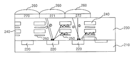
도 2는 본 발명에 의한 반사방지막이 형성된 이미지센서의 일실시예를 나타 내는 것으로서, 반도체 기판(210), 복수의 포토다이오드(220), 층간 절연막(230), 적어도 하나의 금속배선층(240), 반사방지막(250)으로 구성된다.2 illustrates an embodiment of an image sensor having an anti-reflection film according to the present invention, and includes a
복수의 포토다이오드(220)는 반도체 기판(210)의 표면으로부터 소정의 깊이와 소정의 간격을 두고 형성된다. 층간 절연막(230)은 반도체 기판(210) 위에 형성되어 복수의 포토다이오드(220)가 형성된 반도체 기판(210)을 덮는다. 적어도 하나의 금속배선층(240)은 복수의 금속배선을 포함하며, 층간 절연막 내에 소정의 패턴으로 형성된다.The plurality of
반사방지막(250)은 복수의 금속배선층(240) 중에서 최하부 금속배선층의 복수의 금속배선들과 상기 반도체 기판 간, 정확히 표현하자면 복수의 포토다이오드 가장자리의 상부와 금속배선층이 형성되기 전에 각각의 형성될 금속배선층(240) 간의 금속배선들 영역들 사이에 형성된다.The
반사방지막(250)은 폴리 실리콘, 비정질 실리콘, 텅스텐(W), TiN 중에서 적어도 하나의 성분을 포함한다.The
또한, 종래의 반사막은 금속배선보다 큰 사이즈를 가지는데 비해서 본 발명에 의한 반사방지막(250)은 금속배선보다 작은 크기를 갖는다.In addition, while the conventional reflective film has a larger size than the metal wiring, the
도 2를 참조하여 빛의 흐름을 설명하기로 한다.Referring to Figure 2 will be described the flow of light.
마이크로 렌즈(260) 및 녹색, 적색, 청색 각각의 컬러필터(270,271,272)를 투과한 빛이 실리콘 표면으로부터 ① 또는 ②의 경로로 반사되어 상기 금속배선층(240)의 금속배선을 통해 재반사 되더라도 하부에 형성된 빛에 대한 흡수도가 높은 반사방지막(250)에서 빛이 감쇄하게 되어 결국엔 인접한 포토다이오드(220)로 입사 되지 못한다.The light transmitted through the
또한, 입사되더라도 상당히 감소된 광 에너지를 갖게 되므로, ③의 경로로 입사한 빛과 크로스토크를 일으키는 원인을 제거할 수 있게 되며, 또한 ④의 경로를 갖는 빛에 대해서도 MOS 트랜지스터의 전송통로로 입사되는 것을 방지함으로써 종래의 이미지센서의 구조 보다 개선된 이미지를 얻을 수 있게 된다.In addition, since the light energy is significantly reduced, the light incident through the path of ③ and the cause of crosstalk can be eliminated. Also, the light having the path of ④ is incident on the transmission path of the MOS transistor. By preventing the above, it is possible to obtain an improved image than the structure of the conventional image sensor.
도 3은 본 발명에 의한 반사방지막이 형성된 이미지센서의 일실시예를 평면도로 나타낸 것으로, 반사방지막이 제1 금속 배선층(M1)과 제2 금속 배선층(M2) 사이에서 포토다이오드(PD)를 둘러싸고 형성되는 것을 보여준다.3 is a plan view showing an embodiment of an image sensor having an anti-reflection film according to the present invention, wherein the anti-reflection film surrounds the photodiode PD between the first metal wiring layer M1 and the second metal wiring layer M2. Show that it is formed.
본 발명에 의한 반사방지막이 형성된 이미지센서 제조 방법은 다음과 같다.Method of manufacturing an image sensor with an anti-reflection film according to the present invention is as follows.
반도체 기판(210)위에 폴리 실리콘 게이트 및 포토다이오드(220)를 형성한 후 층간 절연막(230)을 증착한다.After forming the polysilicon gate and the
금속 배선층(240)을 형성하기전 층간 절연막(230) 사이에 빛에 대한 흡수도가 높은 물질을 반사방지막(250)의 용도로서 형성한다. 상기 반사방지막(250)은 도 3에서처럼 포토다이오드(220)를 둘러싸는 형태가 될 수 있으며, 물질로는 폴리 실리콘, 비정질 실리콘, 텅스텐(W), TiN 등이 한 예가 될 수 있다.Before forming the
이후 금속배선층(240), 컬러필터(271,272,273) 및 마이크로 렌즈(260)를 형성하면 컬러 크로스토크가 개선된 이미지센서의 제작이 완료된다. Subsequently, when the
이상에서 본 발명에 대한 기술사상을 첨부 도면과 함께 서술하였지만 이는 본 발명의 바람직한 실시예를 예시적으로 설명한 것이지 본 발명을 한정하는 것은 아니다. 또한 본 발명이 속하는 기술 분야에서 통상의 지식을 가진 자라면 누구나 본 발명의 기술적 사상의 범주를 이탈하지 않는 범위 내에서 다양한 변형 및 모방이 가능함은 명백한 사실이다.The technical spirit of the present invention has been described above with reference to the accompanying drawings. However, the present invention has been described by way of example only, and is not intended to limit the present invention. In addition, it is apparent that any person having ordinary knowledge in the technical field to which the present invention belongs may make various modifications and imitations without departing from the scope of the technical idea of the present invention.
본 발명에 의한 반사방지막이 형성된 이미지센서는 상술한 바와 같이 포토다이오드 주위의 상층에 형성된 반사방지막을 통하여 종래의 이미지센서에 비해 컬러 크로스토크 및 노이즈를 감소시키는 것이 가능한 장점이 있다. The image sensor having the anti-reflection film according to the present invention has an advantage in that it is possible to reduce color crosstalk and noise compared to the conventional image sensor through the anti-reflection film formed on the upper layer around the photodiode as described above.
Claims (9)
Priority Applications (3)
| Application Number | Priority Date | Filing Date | Title |
|---|---|---|---|
| KR1020060007579A KR100784725B1 (en) | 2006-01-25 | 2006-01-25 | Image sensor with anti-reflection film and its manufacturing method |
| US12/160,366 US7898011B2 (en) | 2006-01-25 | 2006-12-07 | Image sensor having anti-reflection film for reducing crosstalk |
| PCT/KR2006/005266 WO2007086649A1 (en) | 2006-01-25 | 2006-12-07 | Image sensor having anti-reflection film and method of manufacturing the same |
Applications Claiming Priority (1)
| Application Number | Priority Date | Filing Date | Title |
|---|---|---|---|
| KR1020060007579A KR100784725B1 (en) | 2006-01-25 | 2006-01-25 | Image sensor with anti-reflection film and its manufacturing method |
Publications (2)
| Publication Number | Publication Date |
|---|---|
| KR20070077839A KR20070077839A (en) | 2007-07-30 |
| KR100784725B1 true KR100784725B1 (en) | 2007-12-12 |
Family
ID=38309400
Family Applications (1)
| Application Number | Title | Priority Date | Filing Date |
|---|---|---|---|
| KR1020060007579A Expired - Lifetime KR100784725B1 (en) | 2006-01-25 | 2006-01-25 | Image sensor with anti-reflection film and its manufacturing method |
Country Status (3)
| Country | Link |
|---|---|
| US (1) | US7898011B2 (en) |
| KR (1) | KR100784725B1 (en) |
| WO (1) | WO2007086649A1 (en) |
Families Citing this family (1)
| Publication number | Priority date | Publication date | Assignee | Title |
|---|---|---|---|---|
| KR100953339B1 (en) * | 2007-12-26 | 2010-04-20 | 주식회사 동부하이텍 | Image sensor and manufacturing method |
Citations (2)
| Publication number | Priority date | Publication date | Assignee | Title |
|---|---|---|---|---|
| KR20040007970A (en) * | 2002-07-15 | 2004-01-28 | 주식회사 하이닉스반도체 | Image sensor with improved protection of crosstalk |
| JP2005005540A (en) | 2003-06-12 | 2005-01-06 | Sharp Corp | Solid-state imaging device and manufacturing method thereof |
Family Cites Families (6)
| Publication number | Priority date | Publication date | Assignee | Title |
|---|---|---|---|---|
| KR100533166B1 (en) * | 2000-08-18 | 2005-12-02 | 매그나칩 반도체 유한회사 | CMOS image sensor having low temperature oxide for protecting microlens and method for fabricating the same |
| JP2002198505A (en) * | 2000-12-27 | 2002-07-12 | Nikon Corp | Solid-state imaging device |
| JP2004063778A (en) * | 2002-07-29 | 2004-02-26 | Renesas Technology Corp | Solid-state imaging device |
| JP4794821B2 (en) * | 2004-02-19 | 2011-10-19 | キヤノン株式会社 | Solid-state imaging device and imaging system |
| JP2006190889A (en) * | 2005-01-07 | 2006-07-20 | Fujitsu Ltd | Semiconductor device and manufacturing method thereof |
| US20070052035A1 (en) * | 2005-08-23 | 2007-03-08 | Omnivision Technologies, Inc. | Method and apparatus for reducing optical crosstalk in CMOS image sensors |
-
2006
- 2006-01-25 KR KR1020060007579A patent/KR100784725B1/en not_active Expired - Lifetime
- 2006-12-07 US US12/160,366 patent/US7898011B2/en active Active
- 2006-12-07 WO PCT/KR2006/005266 patent/WO2007086649A1/en not_active Ceased
Patent Citations (2)
| Publication number | Priority date | Publication date | Assignee | Title |
|---|---|---|---|---|
| KR20040007970A (en) * | 2002-07-15 | 2004-01-28 | 주식회사 하이닉스반도체 | Image sensor with improved protection of crosstalk |
| JP2005005540A (en) | 2003-06-12 | 2005-01-06 | Sharp Corp | Solid-state imaging device and manufacturing method thereof |
Also Published As
| Publication number | Publication date |
|---|---|
| US20090008737A1 (en) | 2009-01-08 |
| US7898011B2 (en) | 2011-03-01 |
| WO2007086649A1 (en) | 2007-08-02 |
| KR20070077839A (en) | 2007-07-30 |
Similar Documents
| Publication | Publication Date | Title |
|---|---|---|
| US8669632B2 (en) | Solid-state imaging device and method for manufacturing the same | |
| TWI752159B (en) | Image sensor device and method for manufacturing the smae | |
| KR100874954B1 (en) | Rear receiving image sensor | |
| JP5269409B2 (en) | Image sensor element and method of manufacturing the same | |
| US20140339615A1 (en) | Bsi cmos image sensor | |
| US8610048B2 (en) | Photosensitive integrated circuit equipped with a reflective layer and corresponding method of production | |
| US7755122B2 (en) | Complementary metal oxide semiconductor image sensor | |
| KR20090061310A (en) | Image sensor and its manufacturing method | |
| CN1825603A (en) | Method for improving photonic performance of photosensitive integrated circuits | |
| CN114628420A (en) | Flicker Mitigation Pixel Array Substrate | |
| JP3959734B2 (en) | Solid-state imaging device and manufacturing method thereof | |
| KR20090034429A (en) | Image sensor and its manufacturing method | |
| JP2017011207A (en) | Solid state image pickup device and shielding method | |
| JP2011142330A (en) | Solid-state image sensor, camera module and electronic equipment module | |
| CN100495715C (en) | Image sensing device and manufacturing method thereof | |
| KR101305456B1 (en) | Cmos image sensor having a color microlens and manufacturing method thereof | |
| US20070235771A1 (en) | Semiconductor image sensor and method for fabricating the same | |
| KR100540557B1 (en) | Image sensor manufacturing method for improving optical transmission rate | |
| CN101211948A (en) | Image sensor and manufacturing method thereof | |
| KR100784725B1 (en) | Image sensor with anti-reflection film and its manufacturing method | |
| KR100883038B1 (en) | Image sensor and its manufacturing method | |
| KR101305608B1 (en) | Image sensor | |
| KR20240046947A (en) | Backside illumiated image sensor and method of manufacturing the same | |
| KR20010061056A (en) | Method for fabricating image sensor with improved light sensitivity | |
| CN102891159A (en) | Picture element structure of CMOS (complementary metal oxide semiconductor) image sensor and manufacturing method thereof |
Legal Events
| Date | Code | Title | Description |
|---|---|---|---|
| A201 | Request for examination | ||
| PA0109 | Patent application |
Patent event code: PA01091R01D Comment text: Patent Application Patent event date: 20060125 |
|
| PA0201 | Request for examination | ||
| E902 | Notification of reason for refusal | ||
| PE0902 | Notice of grounds for rejection |
Comment text: Notification of reason for refusal Patent event date: 20070118 Patent event code: PE09021S01D |
|
| E902 | Notification of reason for refusal | ||
| PE0902 | Notice of grounds for rejection |
Comment text: Notification of reason for refusal Patent event date: 20070724 Patent event code: PE09021S01D |
|
| PG1501 | Laying open of application | ||
| E701 | Decision to grant or registration of patent right | ||
| PE0701 | Decision of registration |
Patent event code: PE07011S01D Comment text: Decision to Grant Registration Patent event date: 20071031 |
|
| GRNT | Written decision to grant | ||
| PR0701 | Registration of establishment |
Comment text: Registration of Establishment Patent event date: 20071205 Patent event code: PR07011E01D |
|
| PR1002 | Payment of registration fee |
Payment date: 20071206 End annual number: 3 Start annual number: 1 |
|
| PG1601 | Publication of registration | ||
| G170 | Re-publication after modification of scope of protection [patent] | ||
| PG1701 | Publication of correction | ||
| PR1001 | Payment of annual fee |
Payment date: 20101130 Start annual number: 4 End annual number: 4 |
|
| PR1001 | Payment of annual fee |
Payment date: 20111125 Start annual number: 5 End annual number: 5 |
|
| FPAY | Annual fee payment |
Payment date: 20121205 Year of fee payment: 6 |
|
| PR1001 | Payment of annual fee |
Payment date: 20121205 Start annual number: 6 End annual number: 6 |
|
| FPAY | Annual fee payment |
Payment date: 20131125 Year of fee payment: 7 |
|
| PR1001 | Payment of annual fee |
Payment date: 20131125 Start annual number: 7 End annual number: 7 |
|
| FPAY | Annual fee payment |
Payment date: 20141205 Year of fee payment: 8 |
|
| PR1001 | Payment of annual fee |
Payment date: 20141205 Start annual number: 8 End annual number: 8 |
|
| FPAY | Annual fee payment |
Payment date: 20150921 Year of fee payment: 9 |
|
| PR1001 | Payment of annual fee |
Payment date: 20150921 Start annual number: 9 End annual number: 9 |
|
| FPAY | Annual fee payment |
Payment date: 20160922 Year of fee payment: 10 |
|
| PR1001 | Payment of annual fee |
Payment date: 20160922 Start annual number: 10 End annual number: 10 |
|
| FPAY | Annual fee payment |
Payment date: 20171124 Year of fee payment: 11 |
|
| PR1001 | Payment of annual fee |
Payment date: 20171124 Start annual number: 11 End annual number: 11 |
|
| FPAY | Annual fee payment |
Payment date: 20181126 Year of fee payment: 12 |
|
| PR1001 | Payment of annual fee |
Payment date: 20181126 Start annual number: 12 End annual number: 12 |
|
| FPAY | Annual fee payment |
Payment date: 20191125 Year of fee payment: 13 |
|
| PR1001 | Payment of annual fee |
Payment date: 20191125 Start annual number: 13 End annual number: 13 |
|
| PR1001 | Payment of annual fee |
Payment date: 20201124 Start annual number: 14 End annual number: 14 |
|
| PR1001 | Payment of annual fee |
Payment date: 20221124 Start annual number: 16 End annual number: 16 |
|
| PR1001 | Payment of annual fee |
Payment date: 20241126 Start annual number: 18 End annual number: 18 |