KR100780869B1 - Interconnection pattern design - Google Patents
Interconnection pattern design Download PDFInfo
- Publication number
- KR100780869B1 KR100780869B1 KR1020057021811A KR20057021811A KR100780869B1 KR 100780869 B1 KR100780869 B1 KR 100780869B1 KR 1020057021811 A KR1020057021811 A KR 1020057021811A KR 20057021811 A KR20057021811 A KR 20057021811A KR 100780869 B1 KR100780869 B1 KR 100780869B1
- Authority
- KR
- South Korea
- Prior art keywords
- interconnects
- grid
- pattern
- interconnect pattern
- rows
- Prior art date
- Legal status (The legal status is an assumption and is not a legal conclusion. Google has not performed a legal analysis and makes no representation as to the accuracy of the status listed.)
- Expired - Fee Related
Links
Images


Classifications
-
- H10W72/00—
-
- H10W72/20—
-
- H—ELECTRICITY
- H05—ELECTRIC TECHNIQUES NOT OTHERWISE PROVIDED FOR
- H05K—PRINTED CIRCUITS; CASINGS OR CONSTRUCTIONAL DETAILS OF ELECTRIC APPARATUS; MANUFACTURE OF ASSEMBLAGES OF ELECTRICAL COMPONENTS
- H05K1/00—Printed circuits
- H05K1/02—Details
- H05K1/11—Printed elements for providing electric connections to or between printed circuits
- H05K1/111—Pads for surface mounting, e.g. lay-out
-
- H10W70/65—
-
- H—ELECTRICITY
- H05—ELECTRIC TECHNIQUES NOT OTHERWISE PROVIDED FOR
- H05K—PRINTED CIRCUITS; CASINGS OR CONSTRUCTIONAL DETAILS OF ELECTRIC APPARATUS; MANUFACTURE OF ASSEMBLAGES OF ELECTRICAL COMPONENTS
- H05K2201/00—Indexing scheme relating to printed circuits covered by H05K1/00
- H05K2201/09—Shape and layout
- H05K2201/09209—Shape and layout details of conductors
- H05K2201/09372—Pads and lands
- H05K2201/09418—Special orientation of pads, lands or terminals of component, e.g. radial or polygonal orientation
-
- H—ELECTRICITY
- H05—ELECTRIC TECHNIQUES NOT OTHERWISE PROVIDED FOR
- H05K—PRINTED CIRCUITS; CASINGS OR CONSTRUCTIONAL DETAILS OF ELECTRIC APPARATUS; MANUFACTURE OF ASSEMBLAGES OF ELECTRICAL COMPONENTS
- H05K2201/00—Indexing scheme relating to printed circuits covered by H05K1/00
- H05K2201/10—Details of components or other objects attached to or integrated in a printed circuit board
- H05K2201/10613—Details of electrical connections of non-printed components, e.g. special leads
- H05K2201/10621—Components characterised by their electrical contacts
- H05K2201/10734—Ball grid array [BGA]; Bump grid array
-
- H—ELECTRICITY
- H05—ELECTRIC TECHNIQUES NOT OTHERWISE PROVIDED FOR
- H05K—PRINTED CIRCUITS; CASINGS OR CONSTRUCTIONAL DETAILS OF ELECTRIC APPARATUS; MANUFACTURE OF ASSEMBLAGES OF ELECTRICAL COMPONENTS
- H05K3/00—Apparatus or processes for manufacturing printed circuits
- H05K3/30—Assembling printed circuits with electric components, e.g. with resistor
- H05K3/32—Assembling printed circuits with electric components, e.g. with resistor electrically connecting electric components or wires to printed circuits
- H05K3/34—Assembling printed circuits with electric components, e.g. with resistor electrically connecting electric components or wires to printed circuits by soldering
- H05K3/341—Surface mounted components
- H05K3/3431—Leadless components
- H05K3/3436—Leadless components having an array of bottom contacts, e.g. pad grid array or ball grid array components
-
- H10W72/07236—
-
- H10W72/251—
-
- Y—GENERAL TAGGING OF NEW TECHNOLOGICAL DEVELOPMENTS; GENERAL TAGGING OF CROSS-SECTIONAL TECHNOLOGIES SPANNING OVER SEVERAL SECTIONS OF THE IPC; TECHNICAL SUBJECTS COVERED BY FORMER USPC CROSS-REFERENCE ART COLLECTIONS [XRACs] AND DIGESTS
- Y02—TECHNOLOGIES OR APPLICATIONS FOR MITIGATION OR ADAPTATION AGAINST CLIMATE CHANGE
- Y02P—CLIMATE CHANGE MITIGATION TECHNOLOGIES IN THE PRODUCTION OR PROCESSING OF GOODS
- Y02P70/00—Climate change mitigation technologies in the production process for final industrial or consumer products
- Y02P70/50—Manufacturing or production processes characterised by the final manufactured product
Landscapes
- Engineering & Computer Science (AREA)
- Microelectronics & Electronic Packaging (AREA)
- Electric Connection Of Electric Components To Printed Circuits (AREA)
- Wire Bonding (AREA)
Abstract
기계적인 충격 및 열 순환 하중하에서 개선된 신뢰성을 지닌 상호연결부 패턴 설계가 제공된다. 반도체 요소는 상호연결부 패턴을 형성하기 위하여 행들 및 열들로 정렬되어 있는 복수의 상호연결부들을 포함하는데, 상기 상호연결부들은 상기 패턴이 실질적으로 둥글려지거나 모따기된 모서리들을 구비하도록 정렬된다. 본 발명은 볼 그리드 어레이 패키지들의 개선된 상호연결 수명 및 신뢰성을 제공하고 용이하게 구현된다.Interconnect pattern designs are provided with improved reliability under mechanical shock and thermal cycling loads. The semiconductor element includes a plurality of interconnects arranged in rows and columns to form an interconnect pattern, wherein the interconnects are arranged such that the pattern has substantially rounded or chamfered edges. The present invention provides and is readily implemented an improved interconnect life and reliability of ball grid array packages.
상호연결, 패턴, 반도체, 볼, 그리드, 어레이, 접합 Interconnects, Patterns, Semiconductors, Balls, Grid, Arrays, Junctions
Description
본 발명은 일반적으로 셀 전화 또는 컴퓨터와 같은, 반도체 장치들에 관한 것이다. 특히, 본 발명은 반도체 장치의 수명 및 신뢰성을 연장하고 상기 장치의 필드 불량율(FFR: field failure rate)을 감소시키는 방법에 관한 것이다. 더욱이, 본 발명은 반도체 요소의 상호연결부 패턴 설계에 관한 것이다.The present invention relates generally to semiconductor devices, such as cell phones or computers. In particular, the present invention relates to a method of extending the life and reliability of a semiconductor device and reducing the field failure rate (FFR) of the device. Moreover, the present invention relates to interconnect pattern design of semiconductor elements.
볼 그리드 어레이(BGA: Ball Grid Array) 및 칩 스케일 패키징(CSP: Chip Scale Packaging) 요소들과 같은 반도체 요소들은 반도체 장치들, 특히 셀 전화들과 같은 휴대용 및 핸드 헬드 장치들에서 하나의 중요한 필드 불량 소스이다. CSP들 및 BGA들은 기계적인 충격으로부터의 충격 및 열과 벤딩 사이클로부터의 피로 때문에 고장날 것이다. CSP들 및 BGA들은 요소와 인쇄 배선 기판(PWB: Printed Wired Board) 간의 상호연결의 실패, 즉 상호연결부 또는 PWB 구성 실패로 인해 주로 고장난다. 더욱이, 상호연결부들의 높은 하중은 요소 내부 고장, 예를 들어 기판 또는 다이(die) 파손을 야기할 수 있다.Semiconductor elements such as ball grid array (BGA) and chip scale packaging (CSP) elements are one important field failure in semiconductor devices, particularly portable and handheld devices such as cell phones. Source. CSPs and BGAs will fail due to shock from mechanical shock and fatigue from heat and bending cycles. CSPs and BGAs fail mainly due to the failure of the interconnect between the element and the printed wired board (PWB), that is, the interconnect or PWB configuration failure. Moreover, high loads of interconnects can cause element internal failure, for example substrate or die failure.
일반적인 종래 기술의 반도체 요소들의 예들이 도 1a 내지 도 1e에 도시되어 있다. 특히, 도 1a 내지 도 1e는 상호연결부 패턴을 형성하기 위하여 어떤 2차원 레이아웃으로 배열된 상호연결부들(10)을 구비하는 집적 회로 요소(20)를 도시한 것이다. 상기 상호연결부들(10)은 상기 요소(20)가 인쇄 배선 기판(PWB) 또는 다른 기판의 도전성 선들을 통해 다른 외부 장치들, 다른 주변 장치들 또는 다른 집적 회로들에 전기적으로 연결될 수 있게 하는데 그것에 의해 더 큰 전기 시스템들(예를 들어 컴퓨터, 셀 전화, 텔레비전 등)이 생성될 수 있다. 종래 기술의 도 1a 내지 도 1e에서, 상기 상호연결부들(10)은 모난 모서리들을 지닌 직사각형 모양을 지닌 상호연결부 패턴을 형성하기 위하여 행들 및 열들로 정렬된다. 모든 상호연결부들(10)은 크기가 같지만 상기 상호연결부들 중 몇몇은 더 작거나 더 큰 직경을 가질 수 있다.Examples of general prior art semiconductor elements are shown in FIGS. 1A-1E. In particular, FIGS. 1A-1E illustrate an
고장의 중대한 원인 중 하나는 하중(loading)이 상기 요소의 상호연결부들 간에 균일하게 분포되어 있지 않다는 것이다. 전형적으로 모서리에 있는 상호연결부들은 최고 하중과 접촉하여 먼저 고장난다.One major cause of failure is that the loading is not evenly distributed between the interconnections of the elements. Typically, the interconnects at the corners fail first in contact with the highest load.
열 팽창 계수(CTE) 불일치 및 온도 차이 또는 변동은 요소 및 인쇄 배선 기판(PWB)이 상이한 비율 및 크기로 팽창하게 한다. 도 2는 변형 이전의 인쇄 배선 기판(31)상에 장착된 볼 그리드 어레이 패키지(30)의 단면도를 단순화된 방식으로 도시한 것이고 도 3은 변형 이후에 동일한 것을 도시한 것이다. 요소(32) 중심점으로부터의 거리가 더 멀수록 상호연결부(33)가 받아야 하는 변형 및 스트레스가 더 많다는 것을 알 수 있다. 그러므로, 모서리 솔더(solder) 접합부들(33')은 가장 많이 변형시켜야 하므로 가장 중요한 것들이다.Thermal expansion coefficient (CTE) mismatches and temperature differences or variations cause elements and printed wiring boards (PWB) to expand at different rates and sizes. FIG. 2 shows a cross-sectional view of a ball
기계적인 충격으로부터의 충격 때문에, 인쇄 배선 기판(PWB)은 변형된다. 변형은 지지 구조물들 및 하중에 의존한다. 가속으로 인하여, PWB는 스크류들 사이의 영역에서 위 또는 아래로 구부러진다. 상기 PWB상에 장착된 요소는 상기 변형을 따르는 경향이 있다. 이것은 상기 상호연결부들의 균일하지 않은 하중을 초래하고 상기 요소의 모서리 솔더 접합부들은 가장 많이 하중을 받는다. 도 4 및 도 5는 충격동안의 PWB(40)의 단순화된 예를 도시한 것이다. 충격동안 상기 PWB(40)는 아래로 구부러져 일종의 평평한 그릇을 형성한다. 상기 PWB(40)에 부착된 요소(41)는 한 조각의 유리로서 상상될 수 있는데, 도 4에서와 같이 상기 그릇에 놓여 있다. 추(42)가 상기 유리위에 놓이는데, 이것은 유리(요소)가 그릇(PWB)의 변형을 따라야만 하는 현상을 나타낸다. 첫번째 파손 장소는 상기 추의 바닥 영역에 의존하고 반면에 요소에서 그것은 다이 크기(고정 영역)에 의존한다. 어떤 경우에서도, 가장 고장날 것 같은 위치들은 상기 유리의 모서리들이다. 다른 잠재적인 고장 위치들은 상기 추의 모서리들일 것이다.Because of the impact from the mechanical impact, the printed wiring board PWB is deformed. The deformation depends on the supporting structures and the load. Due to the acceleration, the PWB bends up or down in the region between the screws. Elements mounted on the PWB tend to follow the deformation. This results in uneven loading of the interconnects and the edge solder joints of the element are most heavily loaded. 4 and 5 show simplified examples of the
상기 유리가 도 5에 도시된 바와 같이 둥근 경우, 상기 유리는 전체 가장자리 영역으로부터 지지된다. 거기에서, 스트레스는 균일하고, 가장 중요한 위치들은 아마도 상기 추의 모서리들, 즉 상기 다이 가장자리에 근접한 솔더 접합부들일 것이다. 따라서, 둥글려진 볼아웃(ballout)은 상기 상호연결부들 간에 더 균일하게 하중(loading)을 분포시켜 중요한 솔더 접합부들에서의 스트레스를 감소시키고, 더욱이 신뢰성을 개선할 것이다.When the glass is rounded as shown in FIG. 5, the glass is supported from the entire edge area. There, the stress is uniform and the most important positions are probably the solder joints near the edges of the weight, ie the die edge. Thus, rounded ballout will distribute the load more evenly between the interconnects, reducing stress at critical solder joints, and further improving reliability.
그러므로, CSP 및 BGA 장치들의 조밀성(compactness)이 실질적으로 그리고 불리하게 영향받지 않으면서 전체 제조 신뢰성이 크게 개선되는 상호연결부 패턴을 설계하는 방법이 산업계에 필요하다.Therefore, there is a need in the industry for a method of designing interconnect patterns in which the overall manufacturing reliability is greatly improved without the compactness of CSP and BGA devices being substantially and adversely affected.
본 발명의 주된 목적은 기계적인 충격 및 열 순환 하중하에서 개선된 신뢰성을 지닌, 상호연결부 패턴 설계를 제공하는 것이다. 본 발명에 의한 상호연결부 패턴은 실질적으로 둥글려지거나 모따기된 모서리들을 구비한다. 따라서, 상기 상호연결부들의 신뢰성이 상기 연결부들간의 더 균일한 스트레스 분포 및 더 작은 하중에 의해 개선된다.It is a primary object of the present invention to provide an interconnect pattern design with improved reliability under mechanical shock and thermal cycling loads. The interconnect pattern according to the invention has substantially rounded or chamfered edges. Thus, the reliability of the interconnects is improved by a more uniform stress distribution and smaller loads between the connections.
본 발명의 두번째 주된 목적은 국부적으로 많이 하중을 받는 접합부들이 힘을 상기 요소로 전달하지 않기 때문에, 감소된 요소 내부 하중을 제공하는 것이다. 예를 들어, 요소는 비교적 낮은 힘을 지닌 어떤 유리 부분들을 내부에 가질 수 있다. 그래서 불필요하게 유리에서 스트레스를 증가시키지 않는, 상호연결부 패턴 설계를 가지는 것은 아주 중요하다.The second main object of the present invention is to provide a reduced element internal load since locally heavily loaded joints do not transmit forces to the element. For example, an element may have certain glass parts inside with a relatively low force. So it is very important to have an interconnect pattern design that does not unnecessarily increase the stress in the glass.
상기한 종래 기술의 문제점들을 최소화하고 본 발명의 다른 목적들을 실현하기 위하여 본 발명은 첨부된 독립항들의 특징부들에 제시된 것을 특징으로 한다.In order to minimize the above-mentioned problems of the prior art and to realize other objects of the present invention, the present invention is characterized by the features of the appended independent claims.
본문내의 실시예 예들 및 이점들은 이것이 항상 특별히 언급되지 않을지라도, 적합한 부분들에서 본 발명의 모든 양상들에 적용가능하다.Embodiment examples and advantages in the text are applicable to all aspects of the invention in appropriate parts, although this is not always specifically mentioned.
본 발명에 의하면 둥글려지거나 모따기된 모서리들은 다른 방법들로 달성될 수 있다. 이것을 달성하는 하나의 방법은 모서리들로부터 하나 이상의 전기 연결 상호연결부들을 단순히 생략하거나 모난 상호연결부 패턴 또는 직사각형 상호연결부 패턴의 팁들(tips)을 생략하는 것이다. 다른 방법은 상기 상호연결부 패턴의 가장자리에 하나 이상의 약화된 상호연결부들을 지닌 상호연결부 패턴 설계를 제공하는 것이다. 또 다른 방법은 상기 상호연결부 패턴의 가장자리에 하나 이상의 전기적으로 연결하지 않는 상호연결부들을 지닌 상호연결부 패턴 설계를 제공하는 것이다.According to the present invention rounded or chamfered edges can be achieved in other ways. One way to accomplish this is to simply omit one or more electrical connection interconnects from the corners or omit the tips of the angular interconnect pattern or the rectangular interconnect pattern. Another method is to provide an interconnect pattern design with one or more weakened interconnects at the edge of the interconnect pattern. Another method is to provide an interconnect pattern design having one or more electrically unconnected interconnects at the edge of the interconnect pattern.
본 발명의 몇몇 실시예들은 종속항들에서 설명된다.Some embodiments of the invention are described in the dependent claims.
본 발명은 유사한 참조 번호들이 유사한 요소들을 나타내는 첨부된 도면들에서 예로서 설명되고 이에 한정되지 않는다.The invention is described by way of example and not by way of limitation in the figures of the accompanying drawings in which like reference numerals indicate like elements.
도 1a 내지 도 1e는 종래 기술의 상호연결부 패턴의 평면도를 도시한 것이다.1A-1E show top views of prior art interconnect patterns.
도 2는 인쇄 배선 기판상에 장착된 볼 그리드 어레이 패키지의 단면도를 도시한 것이다.2 illustrates a cross-sectional view of a ball grid array package mounted on a printed wiring board.
도 3은 열 변형 이후에 인쇄 배선 기판상에 장착된 볼 그리드 어레이 패키지의 단면도를 도시한 것이다.3 shows a cross-sectional view of a ball grid array package mounted on a printed wiring board after thermal deformation.
도 4는 충격동안 PWB의 단순화된 예를 도시한 것이다.4 shows a simplified example of a PWB during an impact.
도 5는 충격동안 본 발명에 의한 요소를 포함하는 PWB의 단순화된 예를 도시한 것이다.5 shows a simplified example of a PWB comprising an element according to the invention during an impact.
도 6은 본 발명의 바람직한 제1 실시예에 의한 상호연결부 패턴의 평면도를 도시한 것이다.Figure 6 shows a plan view of an interconnect pattern according to a first preferred embodiment of the present invention.
도 7은 본 발명의 바람직한 제2 실시예에 의한 상호연결부 패턴의 평면도를 도시한 것이다.Figure 7 shows a plan view of an interconnect pattern according to a second preferred embodiment of the present invention.
도 8은 본 발명의 바람직한 제3 실시예에 의한 상호연결부 패턴의 평면도를 도시한 것이다.Figure 8 shows a plan view of an interconnect pattern according to a third preferred embodiment of the present invention.
도 9는 본 발명의 바람직한 제4 실시예에 의한 상호연결부 패턴의 평면도를 도시한 것이다.Figure 9 shows a plan view of an interconnect pattern according to a fourth preferred embodiment of the present invention.
도 10은 본 발명의 바람직한 제5 실시예에 의한 상호연결부 패턴의 평면도를 도시한 것이다.Figure 10 shows a plan view of an interconnect pattern according to a fifth preferred embodiment of the present invention.
도 11은 본 발명의 일 실시예에 의한 상호연결부 패턴 설계 방법의 흐름도를 도시한 것이다.11 is a flowchart illustrating a method of designing an interconnect pattern according to an embodiment of the present invention.
도 12는 본 발명의 바람직한 제6 실시예에 의한 상호연결부 패턴의 평면도를 도시한 것이다.12 illustrates a plan view of an interconnect pattern according to a sixth preferred embodiment of the present invention.
도 13은 본 발명의 바람직한 제7 실시예에 의한 상호연결부 패턴의 평면도를 도시한 것이다.Figure 13 shows a plan view of an interconnect pattern according to a seventh preferred embodiment of the present invention.
도 14, 도 15 및 도 16은 상호연결부 패턴 설계들의 3개의 예들을 도시한 것이다.14, 15, and 16 illustrate three examples of interconnect pattern designs.
도 17은 도 14 내지 도 16에 있는 3개의 설계들에 대한 결과들을 도시한 것이다.17 shows the results for the three designs in FIGS. 14-16.
일반적으로, 본 발명은 반도체 요소, 볼 그리드 어레이(BGA) 및 연장된 열 피로 수명을 지닌 솔더 접합부들을 지닌 반도체 요소를 설계하는 방법을 제공한다. 피로 수명은 상호연결부 패턴을 모서리들로부터 실질적으로 둥글려지거나 모따기되도록 설계함으로써 연장된다. 상호연결부들의 신뢰성은 상기 상호연결부들간의 더 작은 하중 및 더 균일한 스트레스 분포에 의해 개선된다. 둥글려지거나 모따기된 상호연결부 패턴들은 상기 상호연결부들에 의해 형성된 패턴이 둥글려지거나 모따기된 모서리들을 가지도록 상기 상호연결부들을 정렬하여 반도체 요소를 설계함으로써 형성된다.In general, the present invention provides a method of designing a semiconductor element having a semiconductor element, a ball grid array (BGA) and solder joints with extended thermal fatigue life. Fatigue life is extended by designing the interconnect pattern to be substantially rounded or chamfered from the edges. The reliability of the interconnects is improved by smaller loads and more uniform stress distribution between the interconnects. Rounded or chamfered interconnect patterns are formed by aligning the interconnects to design semiconductor elements such that the pattern formed by the interconnects has rounded or chamfered edges.
본 발명에 의한 반도체 요소는 예를 들어 상호연결부 패턴의 모서리들로부터의 다수의 전기 연결 솔더 접합부들(제1상호연결부들)을 상기 패턴의 측면들 또는 상기 패턴의 중앙 또는 상기 패턴의 중앙 근처로 이동시켜 종래 기술의 요소를 변경함으로써 달성될 수 있다. 본 발명에 의한 반도체 요소는 또한 둥글려지거나 모따기된 패턴 설계로 패턴을 설계하기 위하여 상기 패턴의 가장자리에 다수의 솔더 접합부들(제2상호연결부들)을 부가하여 종래 기술의 요소를 변경함으로써 달성될 수 있다. 상기 종래 기술의 요소의 변경 또는 수정없이 본 발명에 의한 상호연결부 패턴을 지니는 신규한 반도체 요소를 설계하는 것이 가능하다는 것은 또한 자명하다.The semiconductor element according to the present invention comprises for example a plurality of electrical connection solder joints (first interconnects) from the corners of the interconnect pattern to the sides of the pattern or the center of the pattern or near the center of the pattern. It can be achieved by changing the elements of the prior art by moving. The semiconductor element according to the invention can also be achieved by adding a number of solder joints (second interconnects) to the edge of the pattern to change the element of the prior art in order to design the pattern in a rounded or chamfered pattern design. Can be. It is also evident that it is possible to design novel semiconductor elements with interconnect patterns according to the invention without changing or modifying the elements of the prior art.
본 발명에 의한 반도체 요소는 또한 상기 상호연결부 패턴의 가장자리에 약화된 복수의 전기적으로 연결하지 않는 상호연결부들(제2상호연결부들)을 부가함으로써 달성될 수 있다. 전기적으로 연결하지 않으며 약화된 상호연결부들은 또한 상기 상호연결부 패턴의 모서리들 또는 팁들(tips)에 배열될 수 있다.The semiconductor element according to the invention can also be achieved by adding a plurality of weakly electrically interconnected interconnects (second interconnects) to the edge of the interconnect pattern. Electrically weakened, weakened interconnects may also be arranged at the corners or tips of the interconnect pattern.
전기적으로 연결하지 않는 상호연결부들(제2상호연결부들)에 의해 상기 접합부들은 상기 반도체 요소의 적합한 기능에 필요하거나 사용되지 않는다는 것을 의미한다. 약화된 상호연결부들(제2상호연결부들)에 의해 상기 접합부들은 전기적으로 기능하도록 유지되는 것을 의미하는 상기 접합부들(제1상호연결부들)보다 실질적으로 더 약하게 형성된다는 것을 의미한다. 전기적으로 연결하지 않으며 약화된 접합부들(제2상호연결부들)은 특히 상호연결부 패턴의 가장자리 또는 상호연결부 패턴의 팁들 또는 모서리들에 배열되는 경우, 최대 스트레스를 받도록 배열될 수 있다. 상기 전기적으로 연결하지 않으며 약화된 상호연결부들(제2상호연결부들)은 상기 반도체 요소 또는 그것이 일부분이 되는 장치의 기능을 손상시키지 않고 손상될 수 있다.By interconnects (second interconnects) that are not electrically connected, this means that the junctions are not needed or used for the proper functioning of the semiconductor element. By weakened interconnects (second interconnects) it means that the junctions are formed substantially weaker than the junctions (first interconnects), which means that they remain electrically functional. Electrically unconnected and weakened joints (second interconnects) may be arranged to receive maximum stress, especially when arranged at the edge of the interconnect pattern or at the tips or corners of the interconnect pattern. The electrically unconnected and weakened interconnects (second interconnects) can be damaged without compromising the function of the semiconductor element or the device to which it is part.
본 발명의 몇몇 실시예들에서 실질적으로 약화된 상호연결부(제2상호연결부)는 그것이 파손되는데 볼-오프(ball-off) 테스트 또는 어떤 필적하는 테스트에서 상기 전기 연결 상호연결부들(제1상호연결부들)에 비해 적어도 10%, 20%, 30%, 40% 또는 50% 더 적은 힘이 필요하다는 것을 의미한다.In some embodiments of the present invention the substantially weakened interconnect (second interconnect) is characterized in that the electrical connection interconnects (first interconnect) in a ball-off test or any comparable test in which it breaks. This means that at least 10%, 20%, 30%, 40% or 50% less force is required.
약화된 상호연결부들은 다른 방법들로 형성될 수 있다. 여기에 몇몇 예들이 제공된다:Weakened interconnects can be formed in other ways. Some examples are provided here:
- 상기 솔더 접합부는 더 작다The solder joint is smaller
- 솔더 마스크 정의(Solder Mask Defined), 즉 SMD 구조의 경우, 더 작은 솔더 마스크 개구부Solder Mask Defined, i.e. smaller solder mask openings for SMD structures
- 특히 비-솔더 마스크 정의(Non-Solder Mask Defined), 즉 NSMD 구조의 경우, 더 작은 솔더 패드들Smaller solder pads, especially for non-solder mask defined, ie NSMD structures
- 산화되거나 그렇지 않으면 비순수 솔더 패드들Oxidized or otherwise non-pure solder pads
- 달리 약화된 금속간 화합물(IMC: InterMetalCompound) 층An otherwise weakened intermetallic compound (IMC) layer
- 솔더링 물질이 다르게 선택될 수 있는데, 즉 더 강한 접합부들과 사용되는 것보다 더 약한 것이 선택될 수 있다.The soldering material may be chosen differently, i.e. weaker than that used with stronger joints.
- 요소 측 또는 PWB 측상의 약하게 부착된 솔더 패드들Weakly attached solder pads on the element side or on the PWB side;
- 솔더 접합부들에 기공(void)을 형성하는 것을 용이하게 하는 상호연결 구조.An interconnect structure that facilitates forming voids in the solder joints.
본 발명은 예를 들어 BGA, 칩 스케일 패키지(CSP: Chip Scale Package) 및 플립 칩(flip chip)과 같은, 예를 들어 솔더 볼들 또는 솔더 범프(bump)와 같은 상호연결부들을 포함하는 어떤 유형의 패키징 기술에서 유용할 수 있다. 본 발명은 또한 예를 들어 C4(Controlled Collapse Chip Connection) 범프 프로세스 또는 E3(Extended Eutectic Evaporative) 범프 프로세스와 같은 상이한 유형의 범프 형성 기술에서 유용할 수 있다. 더욱이, 본 발명은 접합과 같이, 반도체 요소와 그것의 베이스간의 다른 유형의 연결 기술들에서 또한 이용될 수 있다. 따라서 본 발명이 사용되는 연결 기술에 한정되지 않는다는 것은 주목되어야 한다. 본 발명은 도 6 내지 도 17을 참조하여 추가로 설명될 것이다.The invention relates to any type of packaging including interconnects such as solder balls or solder bumps, for example BGA, Chip Scale Package (CSP) and flip chip. May be useful in the art. The present invention may also be useful in different types of bump forming techniques such as, for example, a controlled collapse chip connection (C4) bump process or an extended eutectic evaporative (E3) bump process. Moreover, the present invention can also be used in other types of connection techniques between a semiconductor element and its base, such as a junction. It should therefore be noted that the invention is not limited to the connection technology used. The invention will be further described with reference to FIGS. 6 to 17.
도 6 내지 도 10은 본 발명의 대안적인 몇몇 대안적인 실시예에 의한 상호연결부 패턴의 평면도를 도시한 것이다. 도 6 내지 도 17에서, 상호연결부들(10)은 요소(20)상에 형성되어 있다. 상기 상호연결부들은 상기 요소(20)상에 형성된 전기 회로에 대한 전기 접촉을 가능하게 하기 위하여 일반적으로 상기 요소(20)의 표면에 노출된 어떤 수의 도전성 접촉 영역들이다. 상기 요소(20)는 상기 요소(20)를 인쇄 배선 기판 또는 어떤 다른 기판에 물리적으로 그리고 전기적으로 연결하기 위한 솔더 볼들 및/또는 범프들을 필요로 하는 어떤 장치일 수 있다. 예를 들어, 상기 요소(20)는 BGA 패키지의 기판 부분일 수 있거나, 그것은 플립 칩 기술에서와 같이, PWB에 직접 연결하기 우한 금속 패드들을 지닌 반도체 물질일 수 있다. 상기 요소(20)는 어떤 유형의 표면-장착가능 요소, 예를 들어 플립 칩 요소 또는 LGA, 다중-칩 모듈(MCM), 웨이퍼 스케일 집적 제품 또는 유사한 집적 회로 장치들일 수 있다. 상기 상호연결부들(10)은 알루미늄 또는 구리와 같은 도전성 금속으로 형성될 수 있고, 상기 요소(20)의 외부 연결부들에 대한 단자들로서 사용된다. 도시된 실시예에서, 상기 도전성 접촉 영역들이 일반적으로 원형이라는 것을 주목하라. 하지만, 다른 실시예들에서, 상기 도전성 접촉 영역들은 예를 들어 정방형 또는 직사각형과 같은 다른 모양들을 지닐 수 있다.6-10 illustrate plan views of interconnect patterns according to some alternative embodiments of the present invention. 6 to 17,
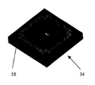
도 6에 도시된 본 발명의 바람직한 제1 실시예에서, 도 1a에 도시된 종래 기술에 의한 상호연결부 패턴은 각 모서리로부터의 하나의 상호연결부를 접합부들의 내부 원 안쪽의 모서리들로 이동시킴으로써 본 발명에 따라 변경되고 설계된다. 따라서, 각 외부 모서리에 있는 하나의 전기 연결 접합부가 빠지게 되지만, 접합부들의 총수는 도 1a에 도시된 바와 같이 종래 기술의 패턴과 동일하고, 상기 그리드 어레이의 맨바깥쪽 행들 및 맨바깥쪽 열들은 모따기된 모서리들을 지닌 패턴의 결과로서 바깥에서 두번째 행들 및 바깥에서 두번째 열들보다 적은 수의 전기 연결 접합부들을 지닌다. 즉, 상기 패턴의 가장자리에 접합부들을 포함하는 외부 루프는 실질적으로 모따기된 모서리들을 지닌다. 도 6 및 또한 도 7 내지 도 17에 도시된 상호연결부들은 솔더 접합부들이다. 하지만 본 발명은 어떤 특정 연결 기술에 한정되지 않기 때문에, 그들은 하나의 가능한 유형의 사용되는 상호연결부에 대한 예를 나타낸다.In a first preferred embodiment of the invention shown in FIG. 6, the interconnect pattern according to the prior art shown in FIG. 1A makes the invention by moving one interconnect from each corner to the corners inside the inner circle of the junctions. It is changed and designed according to. Thus, one electrical connection junction at each outer edge is pulled out, but the total number of junctions is the same as in the prior art pattern as shown in FIG. 1A, with the outermost rows and outermost columns of the grid array being chamfered. As a result of the pattern with rounded corners, there are fewer electrical connection joints than the second row on the outside and the second column on the outside. That is, the outer loop that includes junctions at the edge of the pattern has substantially chamfered edges. The interconnects shown in FIG. 6 and also in FIGS. 7 through 17 are solder joints. However, since the present invention is not limited to any particular connection technology, they represent examples of one possible type of interconnect used.
도 7에 도시된 본 발명의 바람직한 제2 실시예에서, 도 1b에 도시된 바와 같 은 종래 기술에 의한 상호연결부 패턴은 각 모서리에서 6개의 솔더 접합부들의 위치를 변경함으로써 본 발명에 따라 변경되고 설계된다. 2개의 솔더 접합부들은 상기 접합부들의 내부 원 안쪽의 모서리들로 이동된다. 4개의 솔더 접합부들은 상기 패턴의 측면들에 있는 개방 공간으로 이동된다. 따라서, 각 외부 모서리에 복수의 전기 연결 접합부들은 빠져 있지만 접합부들의 총수는 도 1b에 도시된 바와 같은 종래 기술의 패턴과 동일하고, 상기 그리드 어레이의 맨바깥쪽 행들과 맨바깥쪽 열들은 바깥에서 두번째 행들과 바깥에서 두번째 열들보다 적은 수의 전기 연결 접합부들을 지니며 상기 그리드의 바깥에서 두번째 열들은 모따기된 모서리들을 지닌 패턴의 결과로서 상기 그리드의 바깥에서 세번째 행들 및 바깥에서 세번째 열들과 동일한 양 또는 더 적은 수의 전기 연결 접합부들을 지닌다.In a second preferred embodiment of the present invention shown in FIG. 7, the prior art interconnect pattern as shown in FIG. 1B is modified and designed according to the present invention by changing the position of six solder joints at each corner. do. The two solder joints are moved to the corners inside the inner circle of the joints. Four solder joints are moved to the open space on the sides of the pattern. Thus, a plurality of electrical connection junctions are missing at each outer edge but the total number of junctions is the same as in the prior art pattern as shown in FIG. 1B, with the outermost rows and the outermost columns of the grid array being second from outer. Rows and outside of the grid have fewer electrical connections than the second columns and the outside of the grid have the same amount or more as the third row outside and the third column outside of the grid as a result of the pattern with chamfered edges. With fewer electrical connections.
도 8에 도시된 본 발명의 바람직한 제3 실시예에서, 도 1c에 도시된 바와 같은 종래 기술에 의한 상호연결부 패턴은 각각의 맨바깥쪽 모서리로부터의 하나의 상호연결부를 상기 패턴의 측면으로 이동시킴으로써 본 발명에 따라 변경되고 설계된다.In a third preferred embodiment of the present invention shown in FIG. 8, the prior art interconnect pattern as shown in FIG. 1C is provided by moving one interconnect from each outermost corner to the side of the pattern. It is modified and designed according to the present invention.
도 9에 도시된 본 발명의 바람직한 제4 실시예에서, 도 1d에 도시된 바와 같은 종래 기술에 의한 상호연결부 패턴은 각 모서리로부터 6개의 지지 접합부들, 즉 전기 연결 접합부들이 아닌 접합부들을 제거하고, 모서리들로부터의 전기 연결 접합부들을 원래의 접합부 패턴의 측면들로 이동시킴으로써 본 발명에 따라 변경되고 설계된다. 따라서, 상기 상호연결부 패턴의 접합부들은 상기 패턴이 라운드(round) 설계에 근접한, 둥글려진 모서리들을 지니도록 배열된다. 몇몇 실시예들에서 그것 이 라운드 설계를 가지도록 패턴을 설계하는 것이 실제로 가능하다.In a fourth preferred embodiment of the present invention shown in FIG. 9, the prior art interconnect pattern as shown in FIG. 1D removes six support junctions from each corner, i.e., the junctions which are not electrical connection junctions, It is modified and designed according to the invention by moving the electrical connection junctions from the corners to the sides of the original junction pattern. Thus, the junctions of the interconnect pattern are arranged such that the pattern has rounded corners, close to the round design. In some embodiments it is actually possible to design the pattern so that it has a round design.
도 10에 도시된 본 발명의 바람직한 제5 실시예에서, 도 1e에 도시된 바와 같은 종래 기술에 의한 상호연결부 패턴은 접합부 패턴이 둥글려진 모서리들을 지니도록 배열된 부가적인 비 전기 연결 솔더 접합부들을 부가함으로써 본 발명에 따라 변경되고 설계된다. 즉, 부가적인 접합부들은 상기 패턴의 가장자리에 접합부들을 포함하는 상기 패턴의 구성된 외부 루프가 실질적으로 둥글려진 모서리들을 가지도록 부가된다. 도 1e에 도시된 바와 같이, 상기 요소의 다이(die)는 상기 상호연결 부 패턴 외부로 상당히 확장되어 있다. 이것은 상기 요소를 처리하는 경우, 예를 들어 제조시 그리고 기계적 충격 상황에서 상기 다이의 파손을 야기한다, 도 1e는 상기 패턴의 모서리들에서의 지지 접합부들을 도시한 것으로 상기 지지 접합부들이 없는 경우 상기 요소는 제조 라인에서 불안정하게 되고 그것은 처리동안, 예를 들어 리플로우 오븐(reflow oven)에서 기울어질 수 있다. 상기 요소의 기울임은 실패한 솔더 접합을 야기할 수 있다. 하지만, 부가적인 지지 접합부들의 배치는 상기 요소의 다이에 PWB의 변형을 전달하여, 그 결과 상기 다이는 파손될 것이다. 이 문제는 상기 접합 패턴이 둥글려진 모서리들을 지니도록 배치되는, 부가적인 지지 접합부들을 부가함으로써 본 발명에 의한 접합 패턴을 가지고 감소된다.In a fifth preferred embodiment of the present invention shown in FIG. 10, the prior art interconnect pattern as shown in FIG. 1E adds additional non-electrically connected solder joints arranged such that the joint pattern has rounded corners. Thereby being modified and designed according to the invention. That is, additional junctions are added such that the constructed outer loop of the pattern including junctions at the edge of the pattern has substantially rounded corners. As shown in FIG. 1E, the die of the element extends significantly out of the interconnect pattern. This causes breakage of the die when processing the element, for example during manufacture and in mechanical shock situations. FIG. 1E shows the support joints at the corners of the pattern, the element in the absence of the support joints. Becomes unstable in the manufacturing line and it can be tilted during processing, for example in a reflow oven. Tilting the element can cause a failed solder joint. However, the placement of additional support joints will transfer the deformation of the PWB to the die of the element, resulting in the die breaking. This problem is reduced with the joint pattern according to the present invention by adding additional support joints, the joint pattern being arranged to have rounded corners.
도 12는 본 발명의 바람직한 제6 실시예를 도시한 것이다. 상기 요소(20)는 실질적으로 직사각형 상호연결부 패턴에 복수의 상호연결부들(10)을 구비한다. 상기 패턴의 모서리들상에는 전기적으로 연결하지 않으며 동시에 약화된 상호연결부들(50)이 위치한다. 상기 상호연결부들(50)이 파손되는 경우 그것은 상기 요소(20)의 기능에 영향을 미치지 않을 것이다.12 shows a sixth preferred embodiment of the present invention. The
도 13은 본 발명의 바람직한 제7 실시예를 도시한 것이다. 상기 요소(20)는 실질적으로 직사각형 상호연결부 패턴의 중간 부분에 복수의 상호연결부들(10)을 구비한다. 상기 요소(20)의 모든 모서리 근처에 4개의 전기적으로 연결하지 않는 상호연결부들(50)이 위치한다. 상기 상호연결부들(50)은 외부 모서리들이 둥글려지는 방식으로 위치한다. 상기 상호연결부들(50)이 파손되는 경우 그것은 상기 요소(20)의 기능에 영향을 미치지 않을 것이다. 상기 상호연결부들(50) 중 하나 이상의 상호연결부들은 또한 상술된 바와 같이 약화된 상호연결부들일 수 있다. 도 13의 패턴의 중간 부분에 상기 직사각형 상호연결부 패턴의 모서리들상에 약화된 상호연결부들을 배열하는 것이 또한 가능하다.13 shows a seventh preferred embodiment of the present invention. The
도 11은 본 발명의 일 실시예에 의한 상호연결부 패턴 설계 방법의 흐름도를 도시한 것이다. 단계 30에서, 어느 것이 "최악의 경우를 가정한" 솔더 접합부들인지, 즉 상기 설계의 어떤 상호연결부들이 최저 신뢰도를 가지는지 또는 그렇지 않으면 어느 것이 상기 요소 또는 상기 요소-PWB 어셈블리 신뢰도를 감소시키는지를 결정하기 위하여 종래 기술의 반도체 BGA가 분석된다. 단계 32에서, 단계 30에서 결정된 바와 같은 N개의 상호연결부들이 상기 상호연결부 모서리들로부터 상기 패턴의 측면들 또는 상기 패턴의 중앙부 또는 상기 중앙부 근처로 이동되는데, 상기에서 N은 상기 모서리상의 상호연결부들의 총수의 어떤 크기 부분 집합이다. 대안적으로, 단계 32에서, 모따기되거나 둥글려진 모서리들을 지닌 패턴을 생성하기 위하여 N개의 솔더 접합부들이 상기 "최악의 경우를 가정한" 솔더 접합부들 부근에 부가된다. 상술된 바와 같이 약화된 그리고 전기적으로 연결하지 않는 솔더 접합부들을 부가하는 것이 또한 가능하다. 단계 34에서, 상기 변경된 상호연결부 패턴은 상기 요소-PWB 어셈블리 신뢰도를 결정하기 위하여 테스트된다. 도시된 실시예에서, 상기 설계는 유한 요소 방법(FEM: Finite Element Method) 분석을 사용하여 모델링된다. 신뢰도가 허용가능한 양만큼 개선되는 경우, 단계 36에서와 같이 제품의 제조가 허용될 수 있다. 하지만, 신뢰도가 요구되는 양만큼 개선되지 않은 경우, 요구되는 신뢰도가 데몬스트레이션될 때까지 단계 30 내지 단계 34가 반복된다. 상기 방법은 예를 들어 도 6 내지 도 13에 도시된 바와 같이 본 발명의 실시예들을 설계하는데 사용될 수 있다. 예를 들어 도 13에서 상기 방법은 참조 번호 50으로 표시된 모든 연결부들이 약화되고 전기적으로 연결하지 않는 상호연결부들로서 형성되어야 하는지를 계산하는데 사용될 수 있다.11 is a flowchart illustrating a method of designing an interconnect pattern according to an embodiment of the present invention. In
도 14는 종래 기술의 단순한 직사각형 상호연결부 패턴 설계를 지닌 요소(52)를 도시한 것이다. 도 15는 상기 설계의 모든 모서리상에서 모서리에 가장 가까운 곳에 있는 하나의 상호연결부를 제거함으로써 요소(52)로부터 변경된 요소(54)를 도시한 것이다. 상기 제거된 상호연결부는 상기 설계의 새로운 모따기된 모서리(58) 내부에 단지 배열된다. 도 16은 상기 설계의 모든 모서리상에서 모따기된 모서리(58)의 가장 가까운 곳에 있는 두개의 상호연결부들을 제거함으로써 요소(54)로부터 추가로 변경된, 요소(56)를 도시한 것이다. 상기 제거된 상호연결부들은 상기 설계의 새로운 더 모따기된 모서리(60) 내부에 단지 배열되었다.14 shows an
도 17은 도 14 내지 도 16의 3개의 요소들에 대한 드롭(drop) 시뮬레이션으 로부터 획득된 결과들을 나타낸다. 수직축상에 솔더 매트릭스의 최대 스트레스가 도시되어 있다. 상기 스트레스는 "기준"이라고 불리우는, 요소(52)의 직사각형 설계의 모서리에 대한 스트레스의 백분율로서 표시되어 있다. 단지 작게 모따기된 모서리들(58)을 지닌 요소(54)는 "작은 R"로 불리우고 가장 많이 모따기된 모서리들(60)은 "큰 R"로 불리운다. 결과들은 솔더 매트릭스에 대한 물리적인 스트레스가 적합하게 둥글려진 모서리들을 가지고 얼마나 감소하는 지를 명백하게 보여준다.FIG. 17 shows the results obtained from the drop simulation for the three elements of FIGS. 14-16. The maximum stress of the solder matrix on the vertical axis is shown. The stress is expressed as a percentage of stress with respect to the edge of the rectangular design of the
본 발명의 일 실시예에서 둥글려지거나 모따기된 모서리들은 상호연결부 패턴이 볼 그리드 어레이의 각 모서리에서 하나의 접합부 및 바람직하기로는 적어도 두개의 접합부들이 빠져 있는 볼 그리드 어레이로서 형성된다는 것을 의미한다. 몇몇 실시예들에서 전기적 연결 접합부들은 빠져 있지만 실질적으로 약화된 연결부들이 상기 모서리상에 배열된다. 본 발명의 다른 실시예들에서 상기 상호연결부 패턴은 볼 그리드 어레이의 각 모서리에서 적어도 3, 4, 5, 6개 또는 심지어 더 많은 접합부들이 빠져 있는 볼 그리드 어레이로서 형성된다.In one embodiment of the present invention the rounded or chamfered edges mean that the interconnect pattern is formed as a ball grid array with one junction and preferably at least two junctions missing at each corner of the ball grid array. In some embodiments the electrical connection junctions are missing but substantially weakened connections are arranged on the corners. In other embodiments of the invention the interconnect pattern is formed as a ball grid array with at least 3, 4, 5, 6 or even more junctions missing from each corner of the ball grid array.
본 발명의 일 실시예에서 둥글려지거나 모따기된 모서리들은 상기 패턴의 가장자리에서 상기 접합부들을 따라 상호연결부 패턴 가장자리에 포락선을 그리는 경우, 상기 포락선은 단지 둔각을 형성한다. 즉 이 실시예에서 둥글려지거나 모따기된 모서리들은 항상 90도 보다 작다. 다른 실시예들에서 상기 각도들은 80도 미만, 70도 미만, 60도 미만, 50도 미만, 40도 미만, 30도 미만 또는 심지어 20도 미만이다. 예를 들어 도 16의 실시예에서 모서리들의 수는 8이고 그들은 모두 유사한 샤프니스(sharpness)를 갖는다. 따라서 도 16의 패턴 가장자리의 포락선의 모서리들은 45도의 각도를 형성한다.In one embodiment of the present invention, the rounded or chamfered edges form an obtuse angle only when the envelope is drawn at the edge of the interconnect pattern along the junctions at the edge of the pattern. That is, rounded or chamfered edges in this embodiment are always less than 90 degrees. In other embodiments the angles are less than 80 degrees, less than 70 degrees, less than 60 degrees, less than 50 degrees, less than 40 degrees, less than 30 degrees or even less than 20 degrees. For example, in the embodiment of FIG. 16 the number of edges is 8 and they all have similar sharpness. Thus, the corners of the envelope of the pattern edge of FIG. 16 form an angle of 45 degrees.
본 발명은 볼 그리드 어레이의 개선된 상호연결 수명 및 신뢰성을 제공하고 용이하게 구현된다.The present invention provides and is readily implemented an improved interconnect life and reliability of a ball grid array.
본 발명이 우세순이 아닌, 바람직한 실시예들과 관련하여 설명되었을지라도, 본 발명이 수많은 방법들로 변경될 수 있고 특히 상술된 것 이외의 많은 실시예들을 추정할 수 있다는 것은 당업자에에게 명백할 것이다. 따라서, 첨부된 청구항들은 본 발명의 진정한 범위내에 있는, 본 발명의 모든 변형들을 포함할 것이다.Although the invention has been described in connection with the preferred embodiments, not in sequential order, it will be apparent to those skilled in the art that the invention may be modified in numerous ways and in particular that many embodiments other than those described above can be estimated. . Accordingly, the appended claims will include all modifications of the invention that fall within the true scope of the invention.
Claims (31)
Applications Claiming Priority (2)
| Application Number | Priority Date | Filing Date | Title |
|---|---|---|---|
| US10/439,489 US20040227233A1 (en) | 2003-05-16 | 2003-05-16 | Interconnection pattern design |
| US10/439,489 | 2003-05-16 |
Publications (2)
| Publication Number | Publication Date |
|---|---|
| KR20060019541A KR20060019541A (en) | 2006-03-03 |
| KR100780869B1 true KR100780869B1 (en) | 2007-11-29 |
Family
ID=33417812
Family Applications (1)
| Application Number | Title | Priority Date | Filing Date |
|---|---|---|---|
| KR1020057021811A Expired - Fee Related KR100780869B1 (en) | 2003-05-16 | 2004-05-17 | Interconnection pattern design |
Country Status (5)
| Country | Link |
|---|---|
| US (3) | US20040227233A1 (en) |
| EP (1) | EP1625619A1 (en) |
| KR (1) | KR100780869B1 (en) |
| CN (1) | CN1791978A (en) |
| WO (1) | WO2004102661A1 (en) |
Cited By (1)
| Publication number | Priority date | Publication date | Assignee | Title |
|---|---|---|---|---|
| US11855041B2 (en) | 2021-05-06 | 2023-12-26 | Samsung Electronics Co., Ltd. | Semiconductor package and method of manufacturing semiconductor package |
Families Citing this family (12)
| Publication number | Priority date | Publication date | Assignee | Title |
|---|---|---|---|---|
| US7092838B1 (en) * | 2004-06-04 | 2006-08-15 | Sierra Design Automation, Inc. | Method and apparatus for the analysis and optimization of variability in nanometer technologies |
| US20080151512A1 (en) * | 2006-12-22 | 2008-06-26 | Johnson Kenneth W | Enhanced Ball Grid Array Package |
| US20090326864A1 (en) * | 2008-06-27 | 2009-12-31 | Sun Microsystems, Inc. | Determining the reliability of an interconnect |
| JP2010098226A (en) * | 2008-10-20 | 2010-04-30 | Toshiba Corp | Semiconductor device |
| US8415792B2 (en) | 2010-08-04 | 2013-04-09 | International Business Machines Corporation | Electrical contact alignment posts |
| US20120032327A1 (en) * | 2010-08-09 | 2012-02-09 | Fujitsu Limited | Systems and methods for reinforcing chip packages |
| KR102079795B1 (en) | 2013-07-19 | 2020-02-21 | 휴렛-팩커드 디벨롭먼트 컴퍼니, 엘.피. | Image forming apparatus and chip |
| WO2020168552A1 (en) * | 2019-02-22 | 2020-08-27 | Intel Corporation | Joint connection of corner non-critical to function (nctf) ball for bga solder joint reliability (sjr) enhancement |
| US11720726B1 (en) * | 2020-07-24 | 2023-08-08 | Ansys Inc. | Systems and methods of simulating drop shock reliability of solder joints with a multi-scale model |
| US11562952B2 (en) | 2021-01-29 | 2023-01-24 | Cirrus Logic, Inc. | Chip scale package |
| WO2022162330A1 (en) * | 2021-01-29 | 2022-08-04 | Cirrus Logic International Semiconductor Limited | A chip scale package |
| JP2024135354A (en) * | 2023-03-22 | 2024-10-04 | 株式会社東芝 | Semiconductor device and its manufacturing method |
Citations (3)
| Publication number | Priority date | Publication date | Assignee | Title |
|---|---|---|---|---|
| US5557502A (en) * | 1995-03-02 | 1996-09-17 | Intel Corporation | Structure of a thermally and electrically enhanced plastic ball grid array package |
| EP1001462A2 (en) | 1998-11-10 | 2000-05-17 | Nec Corporation | Semiconductor device with connection terminals in the form of a grid array |
| US6274474B1 (en) | 1999-10-25 | 2001-08-14 | International Business Machines Corporation | Method of forming BGA interconnections having mixed solder profiles |
Family Cites Families (8)
| Publication number | Priority date | Publication date | Assignee | Title |
|---|---|---|---|---|
| US555702A (en) * | 1896-03-03 | Electrical measuring-instrument | ||
| US6552425B1 (en) * | 1998-12-18 | 2003-04-22 | Intel Corporation | Integrated circuit package |
| US6444563B1 (en) * | 1999-02-22 | 2002-09-03 | Motorlla, Inc. | Method and apparatus for extending fatigue life of solder joints in a semiconductor device |
| US6207476B1 (en) * | 1999-06-10 | 2001-03-27 | Vlsi Technology, Inc. | Methods of packaging an integrated circuit and methods of forming an integrated circuit package |
| US6291898B1 (en) * | 2000-03-27 | 2001-09-18 | Advanced Semiconductor Engineering, Inc. | Ball grid array package |
| JP4746770B2 (en) * | 2001-06-19 | 2011-08-10 | ルネサスエレクトロニクス株式会社 | Semiconductor device |
| JP3616605B2 (en) * | 2002-04-03 | 2005-02-02 | 沖電気工業株式会社 | Semiconductor device |
| US6762495B1 (en) * | 2003-01-30 | 2004-07-13 | Qualcomm Incorporated | Area array package with non-electrically connected solder balls |
-
2003
- 2003-05-16 US US10/439,489 patent/US20040227233A1/en not_active Abandoned
-
2004
- 2004-05-17 WO PCT/FI2004/000297 patent/WO2004102661A1/en not_active Ceased
- 2004-05-17 CN CNA200480013466XA patent/CN1791978A/en active Pending
- 2004-05-17 KR KR1020057021811A patent/KR100780869B1/en not_active Expired - Fee Related
- 2004-05-17 US US10/847,409 patent/US7223681B2/en not_active Expired - Lifetime
- 2004-05-17 EP EP04733356A patent/EP1625619A1/en not_active Withdrawn
-
2007
- 2007-03-05 US US11/714,671 patent/US20070165388A1/en not_active Abandoned
Patent Citations (3)
| Publication number | Priority date | Publication date | Assignee | Title |
|---|---|---|---|---|
| US5557502A (en) * | 1995-03-02 | 1996-09-17 | Intel Corporation | Structure of a thermally and electrically enhanced plastic ball grid array package |
| EP1001462A2 (en) | 1998-11-10 | 2000-05-17 | Nec Corporation | Semiconductor device with connection terminals in the form of a grid array |
| US6274474B1 (en) | 1999-10-25 | 2001-08-14 | International Business Machines Corporation | Method of forming BGA interconnections having mixed solder profiles |
Cited By (2)
| Publication number | Priority date | Publication date | Assignee | Title |
|---|---|---|---|---|
| US11855041B2 (en) | 2021-05-06 | 2023-12-26 | Samsung Electronics Co., Ltd. | Semiconductor package and method of manufacturing semiconductor package |
| US12113049B2 (en) | 2021-05-06 | 2024-10-08 | Samsung Electronics Co., Ltd. | Semiconductor package and method of manufacturing semiconductor package |
Also Published As
| Publication number | Publication date |
|---|---|
| EP1625619A1 (en) | 2006-02-15 |
| CN1791978A (en) | 2006-06-21 |
| KR20060019541A (en) | 2006-03-03 |
| US7223681B2 (en) | 2007-05-29 |
| WO2004102661A1 (en) | 2004-11-25 |
| US20040251544A1 (en) | 2004-12-16 |
| US20040227233A1 (en) | 2004-11-18 |
| US20070165388A1 (en) | 2007-07-19 |
Similar Documents
| Publication | Publication Date | Title |
|---|---|---|
| US20070165388A1 (en) | Interconnection pattern design | |
| US6444563B1 (en) | Method and apparatus for extending fatigue life of solder joints in a semiconductor device | |
| KR101395365B1 (en) | Dynamic pad size to reduce solder fatigue | |
| US7687803B2 (en) | Semiconductor device and method for manufacturing semiconductor device | |
| US7259453B2 (en) | Hexagonal array structure for ball grid array packages | |
| US6940176B2 (en) | Solder pads for improving reliability of a package | |
| US5859474A (en) | Reflow ball grid array assembly | |
| JP5271088B2 (en) | Microelectronic assembly laminated with ultrafine pitch wiring and manufacturing method thereof | |
| JPH07202378A (en) | Packaged electronic hardware unit | |
| US6410861B1 (en) | Low profile interconnect structure | |
| US9460938B2 (en) | Semiconductor device including a plurality of semiconductor chips, and a cover member with first and second brims | |
| US7714427B2 (en) | Integrated circuit die configuration for packaging | |
| US7462939B2 (en) | Interposer for compliant interfacial coupling | |
| US7994428B2 (en) | Electronic carrier board | |
| US20020109239A1 (en) | Semiconductor device capable of preventing solder balls from being removed in reinforcing pad | |
| US20030207489A1 (en) | Semiconductor device and manufacturing method using a stress-relieving film attached to solder joints | |
| Ho et al. | Linear finite element stress simulation of solder joints on 225 i/o plastic bga package under thermal cycling | |
| JP2001203298A (en) | Semiconductor device and method of manufacturing the same | |
| US7601612B1 (en) | Method for forming solder joints for a flip chip assembly | |
| KR100612783B1 (en) | Semiconductor device | |
| US20240332216A1 (en) | Molded compound patterns on package ball side to mitigate coplanarity and warpage |
Legal Events
| Date | Code | Title | Description |
|---|---|---|---|
| E13-X000 | Pre-grant limitation requested |
St.27 status event code: A-2-3-E10-E13-lim-X000 |
|
| PA0105 | International application |
St.27 status event code: A-0-1-A10-A15-nap-PA0105 |
|
| A201 | Request for examination | ||
| PA0201 | Request for examination |
St.27 status event code: A-1-2-D10-D11-exm-PA0201 |
|
| PG1501 | Laying open of application |
St.27 status event code: A-1-1-Q10-Q12-nap-PG1501 |
|
| E902 | Notification of reason for refusal | ||
| PE0902 | Notice of grounds for rejection |
St.27 status event code: A-1-2-D10-D21-exm-PE0902 |
|
| E13-X000 | Pre-grant limitation requested |
St.27 status event code: A-2-3-E10-E13-lim-X000 |
|
| P11-X000 | Amendment of application requested |
St.27 status event code: A-2-2-P10-P11-nap-X000 |
|
| P13-X000 | Application amended |
St.27 status event code: A-2-2-P10-P13-nap-X000 |
|
| E902 | Notification of reason for refusal | ||
| PE0902 | Notice of grounds for rejection |
St.27 status event code: A-1-2-D10-D21-exm-PE0902 |
|
| P11-X000 | Amendment of application requested |
St.27 status event code: A-2-2-P10-P11-nap-X000 |
|
| P13-X000 | Application amended |
St.27 status event code: A-2-2-P10-P13-nap-X000 |
|
| E701 | Decision to grant or registration of patent right | ||
| PE0701 | Decision of registration |
St.27 status event code: A-1-2-D10-D22-exm-PE0701 |
|
| GRNT | Written decision to grant | ||
| PR0701 | Registration of establishment |
St.27 status event code: A-2-4-F10-F11-exm-PR0701 |
|
| PR1002 | Payment of registration fee |
St.27 status event code: A-2-2-U10-U12-oth-PR1002 Fee payment year number: 1 |
|
| PG1601 | Publication of registration |
St.27 status event code: A-4-4-Q10-Q13-nap-PG1601 |
|
| PR1001 | Payment of annual fee |
St.27 status event code: A-4-4-U10-U11-oth-PR1001 Fee payment year number: 4 |
|
| PR1001 | Payment of annual fee |
St.27 status event code: A-4-4-U10-U11-oth-PR1001 Fee payment year number: 5 |
|
| FPAY | Annual fee payment |
Payment date: 20121031 Year of fee payment: 6 |
|
| PR1001 | Payment of annual fee |
St.27 status event code: A-4-4-U10-U11-oth-PR1001 Fee payment year number: 6 |
|
| FPAY | Annual fee payment |
Payment date: 20131101 Year of fee payment: 7 |
|
| PR1001 | Payment of annual fee |
St.27 status event code: A-4-4-U10-U11-oth-PR1001 Fee payment year number: 7 |
|
| R18-X000 | Changes to party contact information recorded |
St.27 status event code: A-5-5-R10-R18-oth-X000 |
|
| FPAY | Annual fee payment |
Payment date: 20141107 Year of fee payment: 8 |
|
| PR1001 | Payment of annual fee |
St.27 status event code: A-4-4-U10-U11-oth-PR1001 Fee payment year number: 8 |
|
| FPAY | Annual fee payment |
Payment date: 20151016 Year of fee payment: 9 |
|
| PR1001 | Payment of annual fee |
St.27 status event code: A-4-4-U10-U11-oth-PR1001 Fee payment year number: 9 |
|
| R18-X000 | Changes to party contact information recorded |
St.27 status event code: A-5-5-R10-R18-oth-X000 |
|
| FPAY | Annual fee payment |
Payment date: 20161019 Year of fee payment: 10 |
|
| PR1001 | Payment of annual fee |
St.27 status event code: A-4-4-U10-U11-oth-PR1001 Fee payment year number: 10 |
|
| PN2301 | Change of applicant |
St.27 status event code: A-5-5-R10-R11-asn-PN2301 |
|
| PN2301 | Change of applicant |
St.27 status event code: A-5-5-R10-R14-asn-PN2301 |
|
| LAPS | Lapse due to unpaid annual fee | ||
| PC1903 | Unpaid annual fee |
St.27 status event code: A-4-4-U10-U13-oth-PC1903 Not in force date: 20171124 Payment event data comment text: Termination Category : DEFAULT_OF_REGISTRATION_FEE |
|
| PC1903 | Unpaid annual fee |
St.27 status event code: N-4-6-H10-H13-oth-PC1903 Ip right cessation event data comment text: Termination Category : DEFAULT_OF_REGISTRATION_FEE Not in force date: 20171124 |
|
| P22-X000 | Classification modified |
St.27 status event code: A-4-4-P10-P22-nap-X000 |