KR100749899B1 - Power amplifier - Google Patents
Power amplifier Download PDFInfo
- Publication number
- KR100749899B1 KR100749899B1 KR1020040062021A KR20040062021A KR100749899B1 KR 100749899 B1 KR100749899 B1 KR 100749899B1 KR 1020040062021 A KR1020040062021 A KR 1020040062021A KR 20040062021 A KR20040062021 A KR 20040062021A KR 100749899 B1 KR100749899 B1 KR 100749899B1
- Authority
- KR
- South Korea
- Prior art keywords
- power
- output
- amplitude
- signal
- amplifier
- Prior art date
- Legal status (The legal status is an assumption and is not a legal conclusion. Google has not performed a legal analysis and makes no representation as to the accuracy of the status listed.)
- Expired - Fee Related
Links
Images


Classifications
-
- H—ELECTRICITY
- H03—ELECTRONIC CIRCUITRY
- H03F—AMPLIFIERS
- H03F1/00—Details of amplifiers with only discharge tubes, only semiconductor devices or only unspecified devices as amplifying elements
- H03F1/32—Modifications of amplifiers to reduce non-linear distortion
-
- H—ELECTRICITY
- H03—ELECTRONIC CIRCUITRY
- H03F—AMPLIFIERS
- H03F3/00—Amplifiers with only discharge tubes or only semiconductor devices as amplifying elements
- H03F3/72—Gated amplifiers, i.e. amplifiers which are rendered operative or inoperative by means of a control signal
-
- H—ELECTRICITY
- H03—ELECTRONIC CIRCUITRY
- H03F—AMPLIFIERS
- H03F1/00—Details of amplifiers with only discharge tubes, only semiconductor devices or only unspecified devices as amplifying elements
- H03F1/02—Modifications of amplifiers to raise the efficiency, e.g. gliding Class A stages, use of an auxiliary oscillation
- H03F1/0205—Modifications of amplifiers to raise the efficiency, e.g. gliding Class A stages, use of an auxiliary oscillation in transistor amplifiers
- H03F1/0277—Selecting one or more amplifiers from a plurality of amplifiers
-
- H—ELECTRICITY
- H03—ELECTRONIC CIRCUITRY
- H03F—AMPLIFIERS
- H03F3/00—Amplifiers with only discharge tubes or only semiconductor devices as amplifying elements
- H03F3/20—Power amplifiers, e.g. Class B amplifiers, Class C amplifiers
-
- H—ELECTRICITY
- H03—ELECTRONIC CIRCUITRY
- H03F—AMPLIFIERS
- H03F3/00—Amplifiers with only discharge tubes or only semiconductor devices as amplifying elements
- H03F3/20—Power amplifiers, e.g. Class B amplifiers, Class C amplifiers
- H03F3/21—Power amplifiers, e.g. Class B amplifiers, Class C amplifiers with semiconductor devices only
- H03F3/217—Class D power amplifiers; Switching amplifiers
- H03F3/2178—Class D power amplifiers; Switching amplifiers using more than one switch or switching amplifier in parallel or in series
-
- H—ELECTRICITY
- H03—ELECTRONIC CIRCUITRY
- H03F—AMPLIFIERS
- H03F2200/00—Indexing scheme relating to amplifiers
- H03F2200/75—Indexing scheme relating to amplifiers the amplifier stage being a common source configuration MOSFET
Landscapes
- Engineering & Computer Science (AREA)
- Power Engineering (AREA)
- Physics & Mathematics (AREA)
- Nonlinear Science (AREA)
- Amplifiers (AREA)
Abstract
Description
도 1은 종래예의 선형 전력 증폭기의 블록도,1 is a block diagram of a linear power amplifier of a conventional example;
도 2는 F급 증폭 회로의 입출력 전력 특성을 나타내는 그래프,2 is a graph showing input / output power characteristics of a class F amplifier circuit;
도 3은 본 발명의 기본적인 실시예에 따른 전력 증폭기의 블록도,3 is a block diagram of a power amplifier according to a basic embodiment of the present invention;
도 4는 본 발명의 실시예 1에 따른 전력 증폭기의 블록도,4 is a block diagram of a power amplifier according to
도 5는 본 발명의 실시예 2에 따른 전력 증폭기의 블록도,5 is a block diagram of a power amplifier according to Embodiment 2 of the present invention;
도 6은 본 발명의 실시예 3에 따른 전력 증폭기의 블록도,6 is a block diagram of a power amplifier according to Embodiment 3 of the present invention;
도 7은 본 발명의 실시예 7에 따른 전력 증폭기의 블록도,7 is a block diagram of a power amplifier according to a seventh embodiment of the present invention;
도 8은 본 발명의 실시예 1의 전력 증폭기의 입출력 전력 특성을 나타내는 그래프,8 is a graph showing input and output power characteristics of the power amplifier according to the first embodiment of the present invention;
도 9는 본 발명의 실시예 2의 전력 증폭기의 입출력 전력 특성을 나타내는 그래프,9 is a graph showing input / output power characteristics of the power amplifier according to the second embodiment of the present invention;
도 10은 본 발명의 실시예 2의 등가 선형 증폭기의 입출력 전력 특성을 나타내는 그래프,10 is a graph showing input and output power characteristics of the equivalent linear amplifier according to the second embodiment of the present invention;
도 11은 본 발명의 실시예 3의 진폭 조정기에 의한 전력 증폭 유닛의 비선형성을 보상하는 방법을 설명하기 위한 도면,11 is a view for explaining a method for compensating for nonlinearity of a power amplifying unit by an amplitude adjuster of Embodiment 3 of the present invention;
도 12는 본 발명의 실시예 8에 따른 고효율 송신 신호 발생기의 블록도,12 is a block diagram of a high efficiency transmission signal generator according to Embodiment 8 of the present invention;
도 13은 본 발명의 실시예 9에 따른 고효율 송신 신호 발생기의 블록도,13 is a block diagram of a high efficiency transmission signal generator according to Embodiment 9 of the present invention;
도 14는 본 발명의 실시예 10에 따른 고효율 송신 신호 발생기의 블록도,14 is a block diagram of a high efficiency transmission signal generator according to
도 15는 본 발명의 실시예 11에 따른 고효율 송신 신호 발생기의 블록도,15 is a block diagram of a high efficiency transmission signal generator according to Embodiment 11 of the present invention;
도 16은 본 발명의 실시예 12에 따른 고효율 송신 신호 발생기의 블록도,16 is a block diagram of a high efficiency transmission signal generator according to
도 17은 본 발명의 실시예 13에 따른 고효율 송신 신호 발생기의 블록도,17 is a block diagram of a high efficiency transmission signal generator according to Embodiment 13 of the present invention;
도 18은 본 발명의 실시예에 따른 출력 합성 회로의 블록도,18 is a block diagram of an output synthesis circuit according to an embodiment of the present invention;
도 19는 본 발명의 실시예에 따른 가변 출력 정합 회로의 블록도,19 is a block diagram of a variable output matching circuit according to an embodiment of the present invention;
도 20은 본 발명의 실시예에 따른 포화 출력 유닛의 온·오프 구성예에 대한 블록도, 및20 is a block diagram of an on / off configuration example of a saturation output unit according to an embodiment of the present invention; and
도 21은 본 발명의 실시예에 따른 변조 신호와 송신 출력 신호를 나타내는 그래프를 도시한 것이다.21 is a graph illustrating a modulated signal and a transmission output signal according to an embodiment of the present invention.
<도면의 주요 부분에 대한 부호의 설명><Explanation of symbols for main parts of the drawings>
1: 전력 증폭기1: power amplifier
10: 입력 신호10: input signal
11: 출력 신호11: output signal
12: 전력 증폭 유닛12: power amplification unit
15: 진폭 제어 유닛15: amplitude control unit
본 발명은 일반적으로 전력 증폭기에 관한 것이다. 보다 상세하게는, 연속적인 전력 범위에서 출력 전력을 제어할 수 있는 전력 증폭기, 특히 변조 신호를 고효율로 증폭하는 전력 증폭기에 관한 것이다.The present invention relates generally to power amplifiers. More specifically, it relates to a power amplifier capable of controlling output power in a continuous power range, in particular a power amplifier that amplifies a modulated signal with high efficiency.
종래에는, 고효율 증폭을 행하기 위해 복수개의 전력 증폭기 유닛을 병렬로 사용하여 전력 증폭기를 구성하는 기술이 알려져 있다(비특허문헌 1).Conventionally, the technique which comprises a power amplifier using several power amplifier units in parallel in order to perform high efficiency amplification is known (nonpatent literature 1).
도 1은 전력 증폭기의 기본 구성의 종래예를 도시한 것이다. 이 종래의 전력 증폭기는 복수의 F급 증폭 회로로 구성되어 있다. 각 F급 증폭 회로는, 전계 효과 트랜지스터(Field Effect Transistor; 이하 FET라 칭함)와, FET의 드레인에 접속되는 λ/4 전송선과, 캐패시터 C와, 동조 회로와, 부하와, 전압 Vdd로부터의 직류 전원을 FET에 접속하기 위한 RF 쵸크 코일(이하, RFC라 칭함)과, FET에 필요한 신호 입력 레벨을 공급하는 드라이버로 구성되어 있다. 각 F급 증폭 회로의 λ/4 전송선을 출력측에서 결선함으로써, 송신 출력 신호는 복수의 F급 증폭 회로로부터의 출력 신호의 합성이 된다.1 shows a conventional example of the basic configuration of a power amplifier. This conventional power amplifier is composed of a plurality of Class F amplifier circuits. Each Class F amplifier circuit includes a field effect transistor (hereinafter referred to as a FET), a λ / 4 transmission line connected to the drain of the FET, a capacitor C, a tuning circuit, a load, and a voltage V dd . An RF choke coil (hereinafter referred to as RFC) for connecting a DC power supply to the FET and a driver for supplying a signal input level required for the FET. By connecting the λ / 4 transmission lines of the respective Class F amplifier circuits on the output side, the transmission output signals are combined with output signals from the plurality of Class F amplifier circuits.
또한, 드라이버의 출력을 오프로 함으로써 대응하는 F급 증폭 회로의 동작을 정지시킬 수 있다.In addition, by turning off the output of the driver, the operation of the corresponding Class-F amplifier circuit can be stopped.
각 F급 증폭 회로는, 일반적으로 도 2에 도시된 바와 같은 입출력 전력 특성(이하, 입출력 특성이라 칭함), 및 전원 효율(즉, 출력 신호의 전력과 전원이 공급하는 직류 전력의 비, 이하에서는 간단히 효율이라 칭함) 대 입력 전력 특성을 갖는다. 출력 전력이 포화 출력 전력 Ps 부근(또는 입력 전력이 포화 입력 전력 부 근)에 있을 때에는, 높은 효율을 얻을 수 있지만, 입출력 특성은 강한 비선형성으로 되어 버린다. 또한, 입출력 전력이 적은 영역에서는, 입출력 특성은 양호한 선형성을 나타내지만, 효율이 현저히 저하해 버린다.Each F class amplifying circuit generally has an input / output power characteristic (hereinafter referred to as an input / output characteristic) as shown in FIG. 2, and a power supply efficiency (that is, a ratio of the power of the output signal and the DC power supplied by the power, hereinafter). Simply referred to as efficiency) versus input power characteristics. When the output power is near the saturated output power Ps (or the input power is near the saturated input power), high efficiency can be obtained, but the input / output characteristic becomes strong nonlinearity. In addition, in the region where the input / output power is small, the input / output characteristic shows good linearity, but the efficiency is significantly reduced.
도 1에 도시한 종래의 구성은, 주로 일정 진폭(진폭 일정)의 송신 입력 신호의 증폭에 사용되기 때문에, 입출력 특성의 비선형성이 있어도 그다지 문제가 되지 않는다. 그 때문에, 각 F급 증폭 회로를 포화 출력의 상태에서 동작시킴으로써, 고효율을 얻을 수 있다. 도 1의 종래 구성에서는, 동작하는 F급 증폭 회로의 수를 제어함에 의해 복수의 송신 출력 신호의 전력 레벨을 얻을 수 있다. 즉, 송신 전력 제어를 행할 수 있다. 또, 상이한 송신 전력 레벨에서도 고효율이다.The conventional configuration shown in Fig. 1 is mainly used for amplifying a transmission input signal having a constant amplitude (amplitude constant), so that even if there is nonlinearity in input / output characteristics, it is not a problem. Therefore, high efficiency can be obtained by operating each class F amplifier circuit in the state of saturated output. In the conventional configuration of Fig. 1, the power levels of a plurality of transmission output signals can be obtained by controlling the number of Class F amplifier circuits that operate. That is, transmission power control can be performed. It is also highly efficient at different transmit power levels.
또한, 무선 송신기의 송신 주파수 변화에 의한 합성 출력 신호의 상호 변조 왜곡의 악화를 방지하기 위해, 병치 트랜지스터 전력 증폭기의 전단의 가변 감쇠기의 감쇠량을 제어하여, 2개의 트랜지스터 전력 증폭 회로의 동작 상태에 큰 차이가 생기지 않도록 한 종래 기술도 알려져 있다(특허 문헌 1).In addition, in order to prevent the deterioration of the intermodulation distortion of the composite output signal due to the change in the transmission frequency of the radio transmitter, the attenuation amount of the variable attenuator at the front end of the juxtaposition transistor power amplifier is controlled so that the operation state of the two transistor power amplifier circuits is large. The prior art in which a difference does not arise is also known (patent document 1).
[비특허 문헌 1][Non-Patent Document 1]
Alireza Shirvani, David K. Su, and Bruce A. Wooley, "A CMOS RF Power Amplifier With Parallel Amplification for Efficient Power Control, "IEEE JOURNAL OF SOLID-STATE CIRCUITS. VOL.37, NO.6, JUNE 2002Alireza Shirvani, David K. Su, and Bruce A. Wooley, "A CMOS RF Power Amplifier With Parallel Amplification for Efficient Power Control," IEEE JOURNAL OF SOLID-STATE CIRCUITS. VOL.37, NO.6, JUNE 2002
[특허 문헌 1][Patent Document 1]
일본 특허 공개 제2001-237651호 공보Japanese Patent Laid-Open No. 2001-237651
도 1에 도시된 종래 구성으로는, 일정 진폭 신호의 고효율 증폭 및 송신 전력 제어에는 적합하다. 그러나, 진폭이 일정치 않은 신호인 경우의 송신 전력 제어는 전력 레벨이 이산적으로서, 연속적인 전력 레벨을 얻을 수 없다는 문제가 있었다. The conventional configuration shown in Fig. 1 is suitable for high efficiency amplification and transmission power control of a constant amplitude signal. However, the transmission power control in the case of a signal whose amplitude is not constant has a problem that power levels are discrete, and continuous power levels cannot be obtained.
또한, 이 종래 구성을 이용하여 일정치 않은 진폭 신호(진폭이 일정치 않은 신호)의 전력 증폭을 행할 경우에는, 각 F급 증폭 회로의 강한 비선형성에 의해 송신 출력 신호에서 큰 왜곡이 발생해 버린다는 문제도 있었다.In addition, when power amplification of a non-uniform amplitude signal (signal having a constant amplitude) using this conventional configuration, a large distortion occurs in the transmission output signal due to the strong nonlinearity of each Class F amplifier circuit. There was a problem.
더욱이, 진폭이 일정치 않은 신호의 송신 출력 신호의 전력 제어(즉, 그 평균 전력의 제어)를 행할 경우에도, 얻어지는 평균 전력 레벨은 이산적으로서, 연속적인 평균 전력 레벨을 얻을 수 없다는 문제가 있었다.Moreover, even when power control (i.e., control of the average power) of the transmission output signal of the signal whose amplitude is not constant, there exists a problem that the average power level obtained is discrete, and continuous average power level cannot be obtained. .
그래서, 본 발명은 이상 기술한 점을 감안하여 이루어진 것으로, 일정 진폭 신호인 경우에는 연속적인 전력 범위에서 출력 전력을 제어할 수 있는 한편, 일정치 않은 진폭 신호인 경우에는 고효율의 증폭을 행할 수 있는 전력 증폭기를 제공하는 것을 목적으로 하며, 또한 연속적인 전력 범위에서 평균 전력을 제어할 수 있는 전력 증폭기를 제공하는 것을 목적으로 한다.Therefore, the present invention has been made in view of the above description, and in the case of a constant amplitude signal, the output power can be controlled in a continuous power range, while in the case of a non-uniform amplitude signal, high efficiency amplification can be performed. It is an object to provide a power amplifier, and also to provide a power amplifier capable of controlling the average power in a continuous power range.
또한, 출력 대역에서, 일정치 않은 진폭의 출력 신호를, 왜곡을 보다 감소시키고 고효율로 생성할 수 있는 고효율 전력 증폭기를 제공하는 것을 목적으로 한다.It is also an object of the present invention to provide a high-efficiency power amplifier that can produce an output signal of a constant amplitude in the output band, which can further reduce distortion and with high efficiency.
상기 목적을 달성하기 위한 본 발명의 한 특징에 따른 전력 증폭기는, A power amplifier according to a feature of the present invention for achieving the above object,
입력 신호(10)를 입력하고, 상기 입력 신호에 응답하여 증폭한 신호를 출력 신호(11)로서 출력하는 전력 증폭기(1)에 있어서(도 3),In the
상기 입력 신호(10)에 응답하여, 증폭 신호를 출력하도록 병렬로 접속된 N(N은 2 이상의 정수)개의 전력 증폭 유닛(12)과,In response to the
상기 N개의 전력 증폭 유닛(12)으로부터의 각 신호를 합성하고, 상기 전력 증폭기의 출력 신호(11)로서 출력하는 출력 합성 유닛(14)과,An
상기 입력 신호(10)의 진폭에 기초하여, 상기 N개의 전력 증폭 유닛(12) 중에서 동작해야 할 전력 증폭 유닛을 선택하는 진폭 제어 유닛(15)으로 구성된다.Based on the amplitude of the
상기 전력 증폭기에서, 상기 진폭 제어 유닛(15)은, 상기 전력 증폭기의 입력 신호의 진폭을 조정하는 N개의 병렬적인 진폭 조정기와, 상기 출력 신호의 진폭이 상기 입력 신호의 진폭에 대해 실질적으로 연속적인 함수가 되도록, 상기 N개의 전력 증폭 유닛으로부터 동작해야 할 전력 증폭 유닛을 선택하여 동작시키고, 또한 상기 진폭 조정기를 제어하는 제어기로 구성되는 것을 특징으로 해도 좋다.In the power amplifier, the
또한, 상기 전력 증폭기에서, 상기 제어기는 상기 입력 신호의 진폭에 따라 상기 전력 증폭 유닛을 선택하고, 또한 상기 진폭 조정기를 제어하는 것을 특징으로 해도 좋다.In the power amplifier, the controller may select the power amplification unit in accordance with the amplitude of the input signal and further control the amplitude adjuster.
본 발명은, 특히 무선 통신 송신기 내의 전력 증폭기에 적용 가능하지만, 이것에만 한정되는 것은 아니며, 다른 용도의 전력 증폭기에도 적용 가능하다.The present invention is particularly applicable to power amplifiers in wireless communication transmitters, but is not limited thereto, and may be applied to power amplifiers for other purposes.
(기본 실시예)(Basic Example)
도 3에 본 발명의 기본적인 실시예에 따른 전력 증폭기(1)를 도시한다. 전 력 증폭기(1)는 N(N은 2 이상의 정수)개의 전력 증폭 유닛(12), 출력 합성 유닛(14), 진폭 제어 유닛(15)으로 구성되어 있다. 본 실시예에서, 송신 입력 신호(10)의 전력이 진폭 제어 유닛(15)에 의해 조정되며, 조정 후의 전력이 각 전력 증폭 유닛(12)에 공급된다. 진폭 제어 유닛(15)은 입력 신호에 따라, 전력 증폭 유닛(12)의 온/오프의 제어를 행한다. 출력 합성 유닛(14)은 동작하고 있는(즉, 온으로 되어 있는) 각 전력 증폭 유닛(12)으로부터의 출력 신호를 거의 전력합이 되도록 합성하여, 송신 출력 신호(11)로서 출력한다.3 shows a
전력 증폭 유닛(12)은, 예를 들어, FET 등의 증폭 소자를 사용한 증폭 회로어어도 좋다. 그 입출력 특성 및 효율 특성은 일반적으로 도 2에 도시한 F급 증폭기의 특성과 유사하다. 전력 증폭 유닛(12)의 포화 출력 전력을 Ps로 하면, 출력이 그 포화 전력 Ps에 가까울수록 고효율이 된다.The
진폭 제어 유닛(15)은, 마이크로프로세서를 포함한 회로라도 좋고, 송신 입력 신호(10)로부터의 정보를 토대로, 다른 회로 소자를 제어할 수 있다. The
진폭 제어 유닛(15)은 송신 출력 신호(11)의 진폭이 송신 입력 신호(10)의 진폭에 대해 연속 함수가 되도록, N개의 전력 증폭 유닛(12)의 온/오프 제어, 및 그들에 입력되는 신호의 전력 조정 계수를 제어한다.The
(실시예 1)(Example 1)
도 4에 본 발명의 실시예 1에 따른 전력 증폭기(101)를 도시한다. 전력 증폭기(101)는 N(N은 2 이상의 정수)개의 전력 증폭 유닛(112), N개의 진폭 조정기(113), 전력 합성기(114), 제어기(115)로 구성되어 있다. 진폭 제어 유닛(15)은 N 개의 진폭 조정기(113)와 제어기(115)로 구성된다. 본 실시예에서, 송신 입력 신호(110)의 전력이 각 진폭 조정기(113)에 의해 조정되며, 조정 후의 전력이 각 전력 증폭 유닛(112)에 공급된다. 제어기(115)는 각 진폭 조정기(113)의 전력 조정 계수를 제어하고, 또한 전력 증폭 유닛(112)의 온/오프의 제어를 행한다. 전력 합성기(114)는 동작하고 있는(즉, 온으로 되어 있는) 각 전력 증폭 유닛(112)으로부터의 출력 신호를 거의 전력합이 되도록 합성하여, 송신 출력 신호(111)로서 출력한다.4 shows a
전력 증폭 유닛(112)은, 예를 들어, FET 등의 증폭 소자를 사용한 증폭 회로이어도 좋다. 그 입출력 특성 및 효율 특성은 일반적으로 도 2에 도시한 F급 증폭기의 특성과 유사하다. 전력 증폭 유닛(112)의 포화 출력 전력을 Ps로 하면, 출력이 그 포화 전력 Ps에 가까울수록 고효율이 된다.The
제어기(115)는, 마이크로프로세서를 포함한 회로이어도 좋고, 송신 입력 신호(110)로부터의 정보를 토대로, 다른 회로 소자를 제어할 수 있다. The
진폭 조정기(113)는 공지된 어떤 조정기라도 좋으며, 제어기(115)로부터의 제어 신호에 응답하여 송신 입력 신호의 진폭을 조정한다.The
제어기(115)는 송신 출력 신호(111)의 진폭이 송신 입력 신호(110)의 진폭에 대해 연속 함수가 되도록, N개의 전력 증폭 유닛(112)의 온/오프 제어, 및 진폭 조정기(113)의 전력 조정 계수를 제어한다. 이 제어에 대해, 일반성을 상실함이 없이 N=2인 경우에 도 8을 참조하여 설명하기로 한다.The
도 8에 도시한 그래프에서, 곡선 a, b는 각각 전력 증폭 유닛(112-1 및 112- 2)의 입출력 특성을 나타낸다. 송신 입력 신호(110)의 전력과 소망의 송신 출력 신호(111)의 전력과의 관계를, 예를 들어, 곡선 c라 한다. 이 경우, 2개의 전력 증폭 유닛(112-1 및 112-2)의 포화 출력 전력을 각각 Ps1, Ps2(Ps1 < Ps2)로 하고, 각각에 대응하는 입력 전력을 Pa, Pb로 하고, 또한 송신 입력 신호(110)의 전력을 x라 한다.In the graph shown in FIG. 8, curves a and b represent input / output characteristics of the power amplifying units 112-1 and 112-2, respectively. The relationship between the power of the
미리 정해진 입력 전력 레벨 P1, P2, 및 P3에 관해, 송신 입력 신호 전력 x가 x≤P1의 범위에 있는 경우에는, 전력 증폭 유닛(112-1)만이 선택된다. 그리고, 진폭 조정기(113-1)의 전력 조정 계수를 조정함으로써, x가 0 내지 P1까지 변화할 때 전력 증폭 유닛(112-1)으로의 입력이 0 내지 Pa까지 변화하도록 한다. 이에 의해, 전력 증폭 유닛(112-1)이 0 내지 Ps1까지의 전력을 출력하게 된다.Only a predetermined input power levels P 1, P 2, and P 3 is on, when the transmission input signal power x is within the range from x≤P 1, the power amplifying unit 112-1 is selected. Then, by adjusting the power adjustment coefficient of the amplitude adjuster 113-1, the input to the power amplifying unit 112-1 changes to 0 to Pa when x changes from 0 to P 1 . As a result, the power amplifying unit 112-1 outputs power from 0 to Ps 1 .
다음으로, 송신 입력 신호 전력 x가 P1 <x ≤P2 범위에 있는 경우에는, 전력 증폭 유닛(112-2)만이 선택된다. 그리고, 진폭 조정기(113-2)의 전력 조정 계수를 조정함에 의해, x가 P1∼P2까지 변화할 때 전력 증폭 유닛(112-2)의 출력이 Ps 1∼Ps2의 전력을 출력하도록 조정한다.Next, when the transmission input signal power x is in the range of P 1 <x ≦ P 2 , only the power amplifying unit 112-2 is selected. Then, by adjusting the power adjustment coefficient of the amplitude adjuster 113-2, the output of the power amplifying unit 112-2 outputs the power of Ps 1 to Ps 2 when x changes from P 1 to P 2 . Adjust
또한, 송신 입력 신호 전력 x가 P2 <x ≤P3 범위에 있는 경우에는, 전력 증폭 유닛(112-1 및 112-2) 모두 선택되며, 진폭 조정기(113-1 및 113-2)를 모두 조정하는 것에 의해, x가 P2∼P3까지 변화할 때 전력 증폭 유닛(112-1 및 112-2)의 출력 전력의 합이 Ps2∼Ps1+Ps2가 되도록 조정한다.In addition, when the transmission input signal power x is in the range of P 2 <x ≦ P 3 , both the power amplifying units 112-1 and 112-2 are selected, and both the amplitude adjusters 113-1 and 113-2 are turned off. the sum of the output power of the power amplifying unit (112-1 and 112-2) when x is changed to P 2 ~P 3 by adjusting is adjusted so as to be Ps 2 ~Ps 1 + Ps 2.
이에 의해, 송신 출력 신호(111)의 전력이 0 내지 (Ps1+Ps2)의 범위에서, 도 8의 곡선으로 도시한 바와 같이, 연속적인 입출력 특성이 얻어진다. 또, 송신 입력 신호 전력 x가 P1 이상인 범위에서, 전력 증폭 유닛(112-1 및 112-2)의 각각을 포화 출력 전력에 가까운 영역 내에서 동작시키는 것이 가능하므로, 고효율을 얻는 것이 가능하다.As a result, the range of the power of the
일반적으로, 도 4에 도시한 본 실시예의 구성에서는, 출력 전력이 0에서 ΣPsi(Psi는 각 전력 증폭 유닛(112-i)의 포화 출력 전력)까지의 범위에서 연속적인 입출력 특성을 실현할 수 있다. 또한, 송신 입력 신호 전력 x가 Ps1(가령, Ps1<Psi, i=2, 3,…,N) 이상의 범위에서 고효율을 얻는 것이 가능하다. 또, 입출력 전력 특성이 연속 함수인 경우, 입출력 진폭 특성도 연속 함수가 된다.In general, in the configuration of this embodiment shown in Fig. 4, continuous input / output characteristics can be realized in the range of output power from 0 to ΣPs i (Ps i is saturated output power of each power amplifying unit 112-i). have. In addition, it is possible to obtain high efficiency in the range where the transmission input signal power x is equal to or more than Ps 1 (for example, Ps 1 <Ps i , i = 2, 3,..., N). When the input / output power characteristic is a continuous function, the input / output amplitude characteristic also becomes a continuous function.
(실시예 2)(Example 2)
도 5에 본 발명의 실시예 2에 따른 전력 증폭기(102)를 도시한다. 전력 증폭기(102)는 전력 증폭기(101)와 유사하지만, 전력 증폭기(102)에서는, 진폭 조정기(113)와 전력 증폭 유닛(112) 사이에, 전력 증폭 유닛(112)의 비선형성을 보상하기 위한 프리디스토터(Pre-distorter, 이하 PD라 칭함)(116)가 삽입되어 있다. 각 PD(116)와 각 전력 증폭 유닛(112)은 N개의 등가 선형 증폭기(117)를 형성한다. 각 등가 선형 증폭기(117)는 동일한 이득값 G를 갖는다. 도 9에 각 등가 선형 증 폭기(117)의 입출력 특성(곡선 a) 및 그 기초가 되는 전력 증폭 유닛(112)의 입출력 특성(곡선 b)을 도시한다. 전력 증폭 유닛(112)의 포화 출력 전력을 Ps라 하면, 등가 선형 증폭기(117)는 0 내지 Ps까지의 출력 범위에서 직선적인 입출력 특성을 가질 수 있다. 또한, 등가 선형 증폭기(117)의 효율은 특정의 출력 전력(예를 들어, 도 9에 있어서의 P0)에서, 전력 증폭 유닛(112)의 효율과 같다. 이 때문에, 등가 선형 증폭기(117)의 효율은, 출력이 그 최대 출력 전력 Ps에 가까울수록 고효율이 된다.5 shows a
제어기(115)는, N개의 전력 증폭 유닛(112)의 온/오프 제어(즉, 등가 선형 증폭기(117)의 온/오프 제어)를 행하고, 또한 진폭 조정기(113)의 전력 조정 계수를 적절하게 제어한다. 이 제어에 대해, 일반성을 상실하지 않으면서 N=2인 경우에서 도 10을 참조하여 설명하기로 한다.The
2개의 등가 선형 증폭기(117-1 및 117-2)의 최대 출력 전력을 Ps1, Ps2(Ps1
< Ps2)로 하고, 송신 입력 신호(110)의 전력을 x가 x≤(Ps1/G)의 범위에 있는 경우에는, 등가 선형 증폭기(117-1)만이 선택된다. 그리고, 진폭 조정기(113-1)의 전력 조정 계수를 1로 설정한다. 이에 의해, 송신 출력 신호(111)의 전력은 Gx가 된다.The maximum output power of the two equivalent linear amplifiers 117-1 and 117-2 is Ps 1 , Ps 2 (Ps 1 <Ps 2 ), and the power of the
다음으로, 송신 입력 신호 전력 x가 (Ps1/G) < x ≤ (Ps2/G) 범위에 있는 경우에는, 등가 선형 증폭기(117-2)만이 선택된다. 그리고, 진폭 조정기(113-2)의 전력 조정 계수를 1로 설정한다. 이 때의 송신 출력 신호(111)의 전력도 Gx가 된다.Next, when the transmission input signal power x is in the range of (Ps 1 / G) <x ≤ (Ps 2 / G), only the equivalent linear amplifier 117-2 is selected. Then, the power adjustment coefficient of the amplitude adjuster 113-2 is set to one. The power of the
또한, 송신 입력 신호 전력 x가 (Ps2/G) < x ≤ [(Ps1+Ps2)/G] 범위에 있는 경우에는, 등가 선형 증폭기(117-1 및 117-2)가 모두 선택되어 동작하고, 진폭 조정기(113-1 및 113-2)의 전력 조정 계수를 각각 Ps1/ (Ps1+Ps2), Ps
2/ (Ps1+Ps2)로 설정한다. 그 결과, 송신 출력 신호(111)의 전력은 G[Ps1/ (Ps1+Ps2)] x+G [Ps2/ (Ps1+Ps2)] x=Gx가 된다. 따라서, 송신 출력 신호(111)가 0 내지 (Ps1
+Ps2)의 범위에서 선형적인 입출력 특성이 유지된다. 또, 송신 입력 신호 전력 x가 Ps1/G 이상이 되는 경우에서, 등가 선형 증폭기(117-1 및 117-2)는 각각의 최대 출력 전력에 가까운 영역 내에서 동작하므로 고효율이다.Further, when the transmission input signal power x is in the range of (Ps 2 / G) <x ≤ [(Ps 1 + Ps 2 ) / G], the equivalent linear amplifiers 117-1 and 117-2 are both selected. The power adjustment coefficients of the amplitude adjusters 113-1 and 113-2 are set to Ps 1 / (Ps 1 + Ps 2 ) and Ps 2 / (Ps 1 + Ps 2 ), respectively. As a result, the power of the
일반적으로, 도 5에 도시한 본 실시예의 구성에서는, 출력 전력이 0에서 ΣPsi(Psi는 각 등가 선형 증폭기(117-i)의 포화 출력 전력)까지의 범위에서 연속적인 입출력 특성을 실현할 수 있다. 또한, 송신 입력 신호 전력 x가 Ps1/G(가령, Ps1<Psi, i=2, 3,…,N) 이상의 전력 범위에서 고효율을 얻는 것이 가능하다. In general, in the configuration of this embodiment shown in FIG. 5, continuous input / output characteristics can be realized in the range of output power from 0 to ΣPs i (Ps i is saturated output power of each equivalent linear amplifier 117-i). have. In addition, it is possible to obtain high efficiency in a power range in which the transmission input signal power x is equal to or more than Ps 1 / G (for example, Ps 1 <Ps i , i = 2, 3,..., N).
한편, 송신 입력 신호(110)가 일정치 않은 신호인 경우, 제어기(115)는 송신 입력 신호(110)의 순시 전력에 따라 상기와 같이 등가 선형 증폭기(117)의 선택과 진폭 조정기(113)의 제어를 행함으로써, 선형 증폭을 달성할 수 있다.On the other hand, when the
(실시예 3)(Example 3)
도 6에 본 발명의 실시예 3에 따른 전력 증폭기(103)를 도시한다. 전력 증폭기(103)는 전력 증폭기(102)와 유사하지만, 전력 증폭기(103)에서는, 전력 증폭 유닛(112)의 비선형성을 보상하기 위한 PD(116)의 기능이 진폭 조정기(113)에 의해 실행되는 점에서 다르다. 본 실시예에서의 진폭 조정기(113)의 전력 조정량은 전력 증폭 유닛(112)의 비선형성을 보상한 등가 선형 증폭기(119)를 구성하도록 하기 위한 제1 조정량과, 송신 입력 신호(110)의 전력을 등가 선형 증폭기(119)의 입력 범위 내로 조정하기 위한 제2 조정량의 2 부분으로 이루어진다.6 shows a
각 진폭 조정기(113)는 우선, 이득이 G, 최대 출력이 Ps의 등가 선형 증폭기(119)가 형성되어 있는 것으로 하고, 도 5에 도시한 실시예 2와 동일한 방법으로 제2 조정량을 설정한다. 이 제2 조정량에 의해 조정된 후의 송신 입력 신호(110)의 전력을 도 11에서 x1으로 한다. 다음으로, x1에 대응하는 소망의 출력 전력(111)은 Gx1이므로, 조정기(113)는 전력 증폭 유닛(112)이 Gx1을 출력하도록, x
1을 다시 x2로 조정한다. 진폭 조정기(113)의 전체 전력 조정량은 제1 조정량과 제2 조정량의 곱이 된다. Each of the
(실시예 4)(Example 4)
도 5 또는 도 6에 도시된 구성에서, 각 등가 선형 증폭기(117, 119)의 최대 출력 전력을 동일하게 설정할 수도 있다. 이 경우에, 제어기(115)는 이하와 같이 전력 증폭 유닛(112) 및 진폭 조정기(113)를 제어할 수 있다. 즉, 각 등가 선형 증폭기(117, 119)의 최대 출력 전력을 Ps로 하고, r을 1에서 N까지의 정수로 한다. 송신 입력 신호(110)의 전력 x가 [(r-1)Ps/G] < x ≤ (rPs/G)에 있을 때에, r개의 전력 증폭 유닛(112)을 선택하고, 각각에 대응하는 진폭 조정기(113)의 전력 제어 계수를 1/r로 설정한다. 이에 의해, 각각 동작하는 등가 선형 증폭기(117, 119)가 G(1/r)x의 전력을 출력하기 때문에, 송신 출력 신호(111)의 전력은 Gx가 된다.In the configuration shown in Fig. 5 or 6, the maximum output power of each equivalent
또, 상기 x의 범위에서, 각각 동작하는 등가 선형 증폭기(117, 119)의 출력 전력은 [Ps(r-1)/r] 내지 Ps 범위에 있다. r=1인 경우 이외(즉, x가 Ps/G 이상)에서는, 각각 동작하는 등가 선형 증폭기(117, 119)는 최대 출력 전력에 가까운 영역 내에서 동작하므로 고효율이다. 이러한 고효율로 증폭할 수 있는 입출력 전력 범위는 10log(N)(dB)이다.Further, in the range of x, the output powers of the equivalent
(실시예 5)(Example 5)
도 5 또는 도 6에 도시된 구성에서, 각 등가 선형 증폭기(117, 119)의 i(i=1, 2,…N)번째의 최대 출력 전력을 2(i-1)Ps로 설정할 수 있다. 이 경우에서, 제어기(115)는 이하와 같이 전력 증폭 유닛(112) 및 진폭 조정기(113)를 제어할 수 있다. 즉, r을 1에서 (2N-1)까지의 정수로 하면, 송신 입력 신호(110)의 전력 x가 [(r-1)Ps/G] < x≤ (rPs/G)에 있을 때, r을 N자릿수의 2진수로 표현하고, 이 2진수에서 1이 되는 각 자릿수의 번호(단, 그 LSB는 1 자릿수 째, MSB는 N 자릿수 째로 함)에 대응하는 등가 선형 증폭기(117, 119)를 동작시킨다. 그리고, i번째 동작하는 등가 선형 증폭기(117, 119)에 대응하는 진폭 조정기(113)의 전력 조정 계수를 2(i-1)/r로 설정한다. 이에 의해, i번째 동작하는 등가 선형 증폭기(117, 119)는 G[2(i-1)/r]x의 전력을 출력하고, 송신 출력 신호(111)의 전력은 Σ{G[2(i-1)/r]x}(i는 동작하는 등가 선형 증폭기의 번호)이고, Σ2(i-1)= r이므로, 송신 출력 신호(111)의 전력은 결과로서 Gx가 된다.In the configuration shown in FIG. 5 or 6, the i (i = 1, 2, ... N) th maximum output power of each equivalent
또, 상기 x의 범위에서 각각 동작하는 등가 선형 증폭기(117, 119)의 출력 전력은 [Ps(r-1)/r] 내지 Ps의 범위 내에 있다. r=1인 경우 이외(즉, x가 Ps/G 이상)에서는, 각각 동작하는 등가 선형 증폭기(117, 119)는 최대 출력 전력에 가까운 영역 내에서 동작하기 때문에 고효율이다. 이러한 고효율로 증폭할 수 있는 출력 전력의 범위는 10log(2N-1)(dB)이다.The output powers of the equivalent
(실시예 6)(Example 6)
상술된 실시예 중 어느 한 실시예에서, 제어기(115)는 소망의 송신 출력 신호(111)의 평균 전력에 기초하여 진폭 조정기(113)에 대해 전력 조정량 α를 설정할 수 있다. 즉, 제어기(115)는 상술된 실시예에서 도시된 송신 입력 신호(110)의 순시 전력에 따라 설정된 전력 조정 계수와, 전력 조정량 α의 곱을 각 진폭 조정기(113)에 제공할 수있다. 전력 조정량 α는 소망의 송신 출력 신호(111)의 평균 전력에 따라 설정할 수 있다. 본 실시예를 상술한 실시예에 적용한 경우에는, 일정 진폭 신호에 대해, 연속적인 전력 범위에서의 송신 전력 제어를 행할 수 있다. 또한, 본 실시예를 실시예 2 내지 실시예 5에 적용한 경우에는, 일정치 않은 진폭 신호에 대해, 연속적인 전력 범위에서의 송신 전력 제어를 행할 수 있다.In any of the embodiments described above, the
(실시예 7)(Example 7)
도 7에 본 발명의 실시예 7에 따른 전력 증폭기(104)를 도시한다. 전력 증폭기(104)는 도 4에 도시한 전력 증폭기(101)와 유사하지만, 선형 전력 증폭기 (104)에서는, 송신 입력 신호(110)가 송신 전력 제어용 진폭 조정기(118)를 통해 각 진폭 조정기(113)에 공급되는 점이 특징이다. 제어기(115)는, 소망의 송신 출력 신호(111)의 평균 전력에 따라 송신 전력 제어용 진폭 조정기(118)에 일정 전력 조정량 α를 설정할 수 있다. 7 shows a
또, 도 7에서는 도 6의 구성에서 송신 전력 제어용 진폭 조정기(118)를 설치한 예를 도시하고 있지만, 도 4 및 도 5에 도시하는 실시예의 구성에서도 송신 전력 제어용 진폭 조정기(118)를 설치할 수 있다.7 shows an example in which the transmission power
이하에서, 본 발명을 고효율 송신 신호 발생기에 응용한 경우의 실시예를 설명하기로 한다. 그러나, 본 발명은 송신 신호 발생기에 한하지 않고, 소위 각종의 전력 증폭기에 응용 가능하다.Hereinafter, an embodiment in the case where the present invention is applied to a high efficiency transmission signal generator will be described. However, the present invention is not limited to the transmission signal generator but can be applied to so-called various power amplifiers.
(실시예 8)(Example 8)
도 12에 본 발명의 실시예 8에 따른 고효율 송신 신호 발생기(210)를 도시한다. 고효율 송신 신호 발생기(210)는 일정 진폭 국부 발진기(121)와, N(N은 2 이상의 정수)개의 포화 증폭 유닛(212), 출력 합성 회로(214), 진폭 제어부(215)로 구성되어 있다. 진폭 제어 유닛(15)은 진폭 제어부(215)로 구성되며, 전력 증폭 유닛(12)은 포화 증폭 유닛(212)으로 구성되어 있다. 출력 합성 회로(214)로서는, 동작하는 각 포화 증폭 유닛(212)의 출력을 거의 무손실로 합성할 수 있는 것을 이용하는 것이 바람직하다. 포화 증폭 유닛(212)은, 예를 들어, FET를 이용한 F급 증폭 회로 등을 사용할 수 있다. 각 포화 증폭 유닛(212)의 포화 출력 전력을 거의 같게 설정해도 좋고, 서로 다른 포화 출력 전력으로 설정할 수도 있다.12 shows a high efficiency
도 12의 구성에서, 국부 발진기(212)는 일정 진폭 정현파 cos(ωct + φ0)를 출력한다. 여기서, ωc = 2πfc이며, fc는 소정의 주파수이고, φ
0는 초기 위상이다. 일반성을 상실하는 일이 없으므로, φ0 = 0으로 가정하여, 국부 발진기(212)의 출력을 cos(ωct)로 해도 지장은 없다. 변조 신호(210)를 a(t)로 한다. 진폭 제어부(215)는 변조 신호 a(t)의 순시값에 따라 온이 되는 포화 증폭 유닛(212)의 수를 제어한다. 따라서, 온이 되는 포화 증폭 유닛(212)의 수 n은 변조 신호 a(t)의 함수이다.In the configuration of FIG. 12,
도 21을 참조하면서, 온이 되는 포화 증폭 유닛(212)의 개수 n의 설정 방법을 설명하기로 한다. 도 21에서, 일례로서, 포화 증폭 유닛(212)의 개수 N = 4로 한다. 도 21의 (a)는, 변조 신호 a(t)의 파형의 일례를 도시한다. 변조 신호 a(t)의 변조 범위는 도시된 바와 같이 0 내지 a0의 사이로 한다. 온이 되는 포화 증폭 유닛(212)의 수 n을 이하와 같이 설정한다.A method of setting the number n of the saturated amplifying

온이 되는 포화 증폭 유닛(212)은, 국부 발진기(212)의 출력 신호를 증폭하 고, b0 cos(ωct)를 출력한다. 여기서, (1/2)b0
2는 포화 출력 전력이다. 송신 출력 신호(211)를 s(t)로 표현하고, n개의 포화 증폭 유닛(212)이 온이 되는 경우, s(t) = n b0 cos(ωct) = b(t) cos(ωct)가 된다. 여기서, b(t) = nb
o는 s(t)의 포락이다. 도 21의 (b)에 b(t)의 파형을 도시한다. 또한, 도 21의 (b)에 있어서의 파형 c(t)는 도 21의 (a)에 도시하는 변조 신호 a(t)를 (4b0)/a0배로 한 것이며, 소망(所望)의 s(t)의 포락이다. 이하에서, c(t) cos(ωct)를 소망의 송신 출력이라 한다. 한편, b(t)는 c(t)를 양자화한 것이다. 여기서, e(t) = b(t)·c(t)로 하면, e(t)는 오차 성분이며, |e(t)| ≤ (1/2)b0의 성질이 있다. b(t)를 c(t)와 e(t)의 합치라고 볼 수 있다. c(t)의 최대치, 즉 (Nb0)가 미리 정해져 있을 때, N을 증가시킴으로써, b0를 작게 설정할 수 있으므로, 오차 성분 e(t)를 작게 억제시킬 수 있다.The saturated
상기한 설명에서, 각 포화 증폭 유닛(212)의 포화 출력을 같게 하고 있지만, 포화 출력 전력을 b0, 2bo, 4b0,…, 2N-1
b
0와 같이, 2의 멱승 관계로 설정할 수도 있다. 이 경우, 온이 되는 포화 증폭 유닛(212)의 조합에 의해, 0, b0, 2bo, 3b
0,…, 2N-1
b0인 b(t)의 레벨을 얻을 수 있다. 이 경우도, 소요(所要)의 송신 출력 신호 s(t)의 최대 진폭, 즉 (2N-1) b0이 정해진 때, N을 충분히 크게, b
0를 작게 설정함으 로써, 잡음 성분 e(t)의 전력을 규정치 이하로 억제시킬 수 있다.In the above description, the saturation output of each
도 12의 구성에서, 각 포화 증폭 유닛(212)은 온이 된 때 포화점에서 동작하므로, 고효율이다. 각 포화 증폭 유닛(212)이 동일한 효율 η을 갖는 것으로 하면, 도 12의 구성 전체의 효율 ηT는 아래의 수학식 12가 되며, 고효율이다.In the configuration of Fig. 12, each

수학식 2에서, Pi는 온이 되는 포화 증폭 유닛(212)의 출력 전력을 나타낸다.In Equation 2, P i represents the output power of the saturated
또, 도 12의 구성에서, 송신 출력 신호(211)는 변조 신호(210)에 의해 변조된 진폭 변조파(AM파)이다.12, the
(실시예 9)(Example 9)
도 13에 본 발명의 실시예 9에 따른 고효율 송신 신호 발생기(202)를 도시한다. 실시예 9에서는, 고효율 송신 신호 발생기(202)는 일정 진폭 국부 발진기(212), N(N은 2 이상의 정수)개의 포화 증폭 유닛(212), 출력 합성 회로(214), 및 진폭 제어부(215)로 구성되며, 또한, 극좌표 변조 처리부(216)와, 위상 변조기(217)로 구성되어 있다. 도 12의 실시예 8의 구성과 비교해 보면, 실시예 9에서는, 변조 신호(210)를 진폭 성분(218)과 위상 성분(219)으로 분해하여 출력하는 극 좌표 변조 처리부(216)와, 위상 변조부(217)가 새로이 설치된 점이 다르다.13 shows a high efficiency
변조 신호(210)는 복소 신호로서, a(t) exp(jφ(t))로 표현된다. 여기서, a(t)와 φ(t)는 각각 변조 신호(210)의 진폭 성분과 위상 성분이다. 극좌표 변조 처리부(216)는 변조 신호(210)의 변조 성분(218)과 위상 성분(219)을 분리하여, 진폭 성분 a(t)와 위상 성분 φ(t)를 출력한다. 위상 변조부(217)에서, 국부 발진기(212)의 출력 신호 cos(ωct)를 φ(t)에 의해 위상 변조하여, 위상 변조파 cos(ωct) + φ(t)를 출력한다. 이 위상 변조파는, 또한 도 12의 실시예 8에서 설명한 처리와 동일하게, 복수의 포화 증폭 유닛(212), 출력 합성 회로(214) 및 진폭 제어부(215)에 의해, a(t)에 의해 진폭 변조가 행해진다. 결과적으로, 송신 출력 신호(211)는 변조 신호(210)에 의해 진폭·위상 변조된 변조파 a(t) cos(ωct + φ(t)),즉 직교 진폭 변조파(QAM파)가 된다.The modulated
또, 각 포화 증폭 유닛(212)은 온으로 된 때 포화점에서 동작하므로, 고효율이다. 도 13의 구성 전체의 효율 ηT는 동일하게 수학식 2로 표현되고, ηT = η으로 되므로, 고효율이 된다.Moreover, since each
(실시예 10)(Example 10)
도 14에 본 발명의 실시예 14에 따른 고효율 송신 신호 발생기(203)를 도시한다. 도 12에 도시한 실시예 8의 구성과 비교해 보면, 실시예 10에서는, 진폭 변조부(220)와 선형 증폭 유닛(221)이 새로이 설치된 점이 다르다. 도 21을 참조하여 본 실시예를 설명하기로 한다. 도 14의 구성에서, 가령 선형 증폭 유닛(221)의 출력을 고려하지 않는 것으로 하면, 송신 출력 신호(211)의 진폭은 도 21의 (b)에 도시하는 b(t)가 된다. 선형 증폭 유닛(221)의 이득을 k로 한다. 진폭 제어부(215)는 상술한 e(t) = b(t)·c(t)를 -(1/k) e(t)의 형으로 진폭 변조부(220)에 제공한다. 진폭 변조부(220)는 국부 발진기(212)의 출력에 대해, -(1/k) e(t)에 의해 진폭 변조를 행하여 -(1/k) e(t) cos(ωct)를 출력한다. 이것을 위해서, 선형 증폭 유닛(221)은 -e(t) cos(ωct)를 출력한다. 이것을 계산에 넣으면, 송신 출력 신호(211)의 진폭은 -e(t) + b(t) = c(t)가 된다. 여기서, c(t)는 상술한 소망의 s(t)의 포락이다. 따라서, 도 14에 도시하는 실시예 10의 구성에서는 송신 출력 신호(211)는 소망의 송신 출력이 된다.14 shows a high efficiency
도 14의 구성 전체의 효율 ηT는, ηT = {Ps(t)/(PDC
1
+ PDC
2)}이 된다. 여기서, Ps(t) = (1/2) c2(t)이며, PDC
1은 선형 증폭기(21)에서 소비되는 직류 전력이며, PDC2는 온이 되는 각 포화 증폭 유닛(212)에서 소비되는 직류 전력의 합이다. 각 포화 증폭 유닛(212)의 효율이 동일하게 η인 경우, PDC
2 = (1/2) b2(t)/η ≒ Ps(t)/η이 된다. 이에 의해, ηT는The efficiency η T of the entire configuration in FIG. 14 becomes η T = {P s (t) / (P DC 1 + P DC 2 )}. Where P s (t) = (1/2) c 2 (t), P DC 1 is the DC power consumed in the linear amplifier 21, and P DC2 is in each
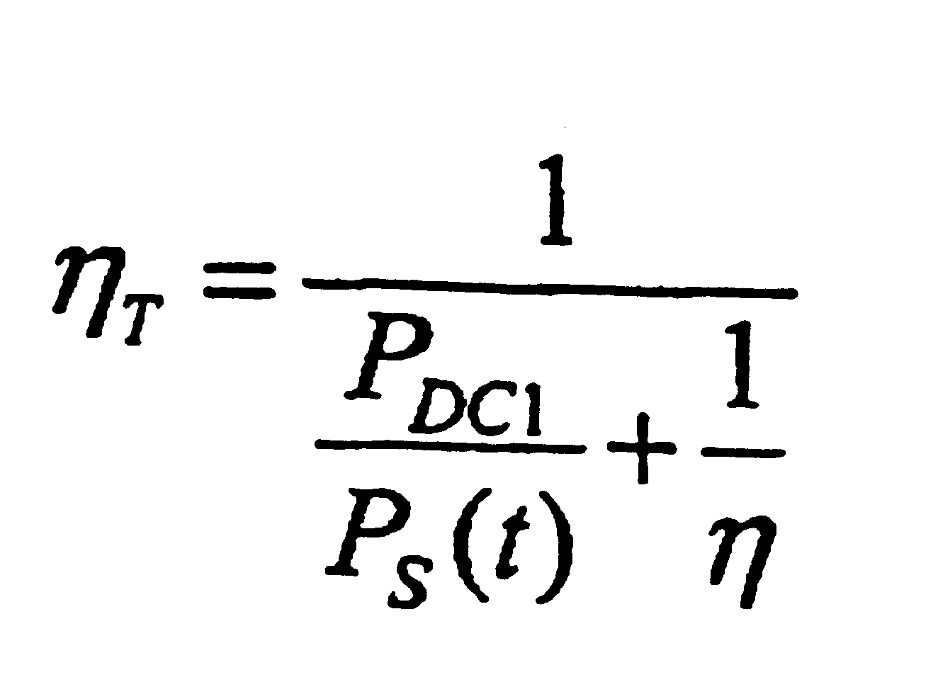
이 된다. 수학식 3에서, Ps(t)는 시간적으로 변화하므로, ηT도 시간적으로 변화하지만, 그 시간 평균인 ηT(시간 평균)은,Becomes In Equation 3, since P s (t) changes in time, η T also changes in time, but the time average η T (time average) is

이 된다. 일반적으로 선형 증폭기의 효율은 낮지만, 도 12에 도시한 실시예 8에서 설명한 바와 같이, 포화 증폭 유닛(212)의 수 N을 증가시킴에 의해, e(t)를 작게 억제할 수 있으므로, 선형 증폭 유닛(221)의 출력 신호를 매우 작게 할 수 있다. 이 경우, 선형 증폭 유닛(221)의 효율이 낮더라도, PDC
1은 매우 작다. 이 때문에, 수학식 4에서, ηT(시간 평균) ≒ η이 된다. 따라서, 평균적으로 보면, 도 14의 실시예 10의 구성 전체의 효율은 고효율이 된다.Becomes In general, although the efficiency of the linear amplifier is low, by increasing the number N of the
(실시예 11)(Example 11)
도 15에 본 발명의 실시예 11에 따른 고효율 송신 신호 발생기(204)를 도시 한다. 도 13에 도시한 실시예 9의 구성과 비교해 보면, 실시예 11에서는 진폭 변조부(220)와 선형 증폭 유닛(221)을 새로이 설치한 점이 다르다. 또한, 도 14에 도시한 실시예 10의 구성과 비교해 보면, 실시예 11에서는 국부 발진기(212)로부터의 출력 신호가 위상 변조기(217)에 의해 위상 변조가 실행되고 나서 각 포화 증폭 유닛(212) 및 진폭 변조부(220)에 공급되는 점이 다르다. 진폭 변조부(220)와 선형 증폭 유닛(221)의 동작은 도 14의 실시예 10과 동일하다.15 shows a high efficiency
본 실시예의 경우, 선형 증폭 유닛(221)은 -e(t) cos(ωct + φ(t))를 출력하고, 송신 출력 신호(211)는 c(t) cos(ωct + φ(t))로 되어, 소망의 송신 출력이 된다. 또한, 도 14에 도시한 실시예 10에서 설명한 이유와 동일하게, 도 15의 구성 전체의 효율은 평균적으로 보면 고효율이다.In the present embodiment, the
(실시예 12)(Example 12)
도 16에 본 발명의 실시예 12에 따른 고효율 송신 신호 발생기(205)를 도시한다. 도 12에 도시한 실시예 8의 구성과 비교해 보면, 실시예 12에서는 출력 합성 회로(214)의 후단에 대역 제한 필터(230)를 새로이 설치하고, 대역 제한 필터(230)로부터의 송신 출력 신호가 되는 점이 다르다.16 shows a high efficiency
실시예 12의 구성에서, 대역 제한 필터(230)는 송신 신호 대역외에 있어서의 상술한 오차 성분 e(t)의 주파수 성분을 제거시킴으로써, 송신 출력 신호(211)의 포락을 평활하게 함과 함께, 포화 증폭 유닛(212)으로부터 출력되는 고주파 성분을 제거한다. 실시예 12의 구성과 동일하게, 도 13의 실시예 9의 구성에 대해서도 출 력 합성 회로(214)의 후단에 평활화(smoothing) 필터(230)를 설치할 수 있다.In the configuration of the twelfth embodiment, the
또, 도 14 및 도 15에 도시하는 실시예 10 및 실시예 11의 구성에 대해서도, 출력 합성 회로(214)의 후단에 평활화 필터 또는 대역 제한 필터(230)를 설치할 수 있다. 이들 경우, 대역 제한 필터(230)는 포화 증폭 유닛(212)으로부터 출력되는 고주파 성분을 제거한다.The smoothing filter or the
(실시예 13)(Example 13)
도 17에 본 발명의 실시예 13에 따른 고효율 송신 신호 발생기(206)를 도시한다. 도 12에 도시한 실시예 8의 구성과 비교해 보면, 실시예 13에서는 출력 합성 회로(214)가 진폭 제어부(215)에 의해 제어되는 점이 다르다.17 shows a high efficiency
실시예 13의 구성에서, 진폭 제어부(215)는 각 포화 증폭 유닛(212)의 온/오프에 따라 출력 합성 회로(214)의 전기적 특성을 조정하고, 출력 합성 회로(214)에 있어서의 전력 손실을 매우 작게 억제시킨다.In the configuration of the thirteenth embodiment, the
(기타 실시예)(Other Examples)
도 18에 본 발명의 기타 실시예에 따른 고효율 송신 신호 발생기에 사용되는 출력 합성 회로의 예를 도시한다. 상기 실시예 8 내지 실시예 11 중 어느 한 실시예에서, 출력 합성 회로(214)는, 예를 들어, 도 18의 (a)에 도시하는 구성을 사용할 수 있다. 도 18의 (a)에 도시하는 출력 합성 회로(214)는 각 포화 증폭 유닛(212)으로부터의 출력을 단순히 결선하여 출력하는 전류 합성 회로이다.18 shows an example of an output synthesis circuit used in the high efficiency transmission signal generator according to another embodiment of the present invention. In any of the eighth to eleventh embodiments, the
도 18의 (b)는, 출력 합성 회로(214)의 다른 구성예를 도시한다. 도 18의 (b)에 도시하는 출력 합성 회로(214)는 각 포화 증폭 유닛(212)으로부터의 출력을 결선하여 합성한 후, 출력 정합 회로(280)를 통해 출력한다.18B illustrates another example of the configuration of the
도 18의 (c)는, 출력 합성 회로(214)의 또 다른 구성예를 도시한다. 상기 실시예 8 내지 실시예 11 중 어느 한 실시예에서, 출력 합성 회로(214)는 도 18의 (c)에 도시하는 구성을 사용할 수 있다. 도 18의 (c)에 도시하는 출력 합성 회로(214)는 각 포화 증폭 유닛(212)으로부터의 출력을 결선하여 합성한 후, 가변 출력 정합 회로(281)를 통해 출력한다. 가변 출력 정합 회로(281)는 진폭 제어부(215)로부터의 제어에 의해, 각 포화 증폭 유닛(212)의 온/오프에 따라 그 전기적 특성을 조정함으로써 출력 합성 회로(214)에서의 전력 손실을 매우 작게 억제시킨다.FIG. 18C shows another configuration example of the
도 19는 도 18에 도시한 가변 출력 정합 회로(281)의 구성의 일례를 도시한다. 도 19에 도시한 가변 출력 정합 회로(281)는 병렬로 설치되는 복수개의 개방 또는 접지 리액턴스(282)로 구성된다. 리액턴스(282)의 개방 또는 접지 상태의 전환은, 진폭 제어부(215)에 의해 제어되는 스위치(283)의 전환에 의해 행해진다. 가변 출력 정합 회로(281)의 전기적 특성은 접지되는 병렬 리액턴스(282)의 개수(個數) 변화에 의해 조정된다.FIG. 19 shows an example of a configuration of the variable
도 20은 상기 실시예 중 어느 한 실시예에서 진폭 제어부(215)에 의해 포화 증폭 유닛(212)의 온/오프를 제어하기 위한 구체적 구성의 예를 도시한다. 예를 들어, 도 20의 (a)에 도시하는 구성에서, 포화 증폭 유닛(212)은 포화 증폭기(300)와 그 RF 입력측에 설치되는 RF 스위치(301)로 구성된다. 진폭 제어부(215)는 RF 스위치(301)의 진폭 제어 입력 단자를 통해 RF 스위치(301)의 온/오프를 제어한다. 이에 의해, 포화 증폭 유닛(212)의 온/오프가 달성된다.20 shows an example of a specific configuration for controlling the on / off of the
도 20의 (b)에 도시하는 다른 구성에서, 포화 증폭 유닛(212)은 포화 증폭기(300)와 바이어스 제어 회로(302)로 구성된다. 진폭 제어부(215)는 바이어스 제어 회로(302)의 진폭 제어 입력 단자를 통해 바이어스 제어 회로(302)의 상태를 제어함으로써, 포화 증폭 유닛(212)의 온/오프를 달성한다.In another configuration shown in FIG. 20B, the
본 발명에 따른 전력 증폭기에 의하면, 출력 전력을 입력 전력에 대해 연속적인 함수로 할 수 있으며, 그 결과, 송신 전력 제어를 연속적인 전력 범위이며 또한 고효율로 행할 수 있다.According to the power amplifier according to the present invention, the output power can be a continuous function with respect to the input power, and as a result, the transmission power control can be performed in a continuous power range and with high efficiency.
본 발명의 일 실시예에 따른 전력 증폭기에 의하면, 각 전력 증폭 유닛의 입출력 특성의 비선형을 보상하여 등가 선형 증폭기를 구성하고, 또한 입력 신호의 순시 전력에 따라 등가 선형 증폭기를 결합함으로써, 선형이며 고효율의 전력 증폭기를 구성할 수 있다. 이로써, 일정치 않은 진폭의 송신 입력 신호에 대해서도, 고효율이며 선형적인 진폭을 달성할 수 있다. 또한, N개의 전력 증폭 유닛을 사용한 경우에서, N을 크게 함에 의해, 고효율이며 증폭 가능 입출력 전력 범위를 확대시킬 수도 있다. 이 특징은, 피크 대 평균 전력이 큰 일정치 않은 진폭 신호를 증폭하는 경우에 특히 유리하다. 또한, 이 경우에, 입력 신호의 평균 전력을 조정함으로써 출력 신호의 평균 전력을 연속적으로 제어할 수 있다.According to the power amplifier according to an embodiment of the present invention, an equivalent linear amplifier is configured by compensating for the nonlinearity of the input / output characteristics of each power amplifying unit, and by combining the equivalent linear amplifier according to the instantaneous power of the input signal, it is linear and high efficiency. The power amplifier of can be configured. This makes it possible to achieve a high efficiency and linear amplitude even with a transmission input signal having a constant amplitude. In the case of using N power amplification units, by increasing N, the high efficiency and amplifiable input / output power range can be expanded. This feature is particularly advantageous when amplifying non-uniform amplitude signals with large peak-to-average power. In this case, the average power of the output signal can be continuously controlled by adjusting the average power of the input signal.
또한, 본 발명의 다른 실시예에 따른 전력 증폭기에 의하면, 변조 신호의 진폭에 따라 동작하는 포화 증폭 유닛의 수를 제어함으로써, AM 변조파 또는 QAM 변조파의 송신 출력 신호를 발생할 수 있다. 또한, 각 포화 증폭 유닛이 국부 발진 기로부터의 일정 진폭 신호만을 증폭하므로, 고효율로 동작한다. 따라서, 본 발명 실시예 구성의 전체도 고효율이 된다. 또한, 포화 증폭 유닛의 수를 충분히 설치함에 의해, 또는 오차 성분을 보상하기 위한 선형 증폭 유닛을 설치함에 의해, 송신 대역에서 왜곡이 적은 출력 신호를 생성할 수 있다.Further, according to the power amplifier according to another embodiment of the present invention, by controlling the number of saturation amplification units operating in accordance with the amplitude of the modulated signal, it is possible to generate a transmission output signal of the AM modulated wave or QAM modulated wave. In addition, since each saturation amplification unit amplifies only a constant amplitude signal from the local oscillator, it operates with high efficiency. Therefore, the whole structure of the embodiment of the present invention is also highly efficient. Further, by providing a sufficient number of saturation amplifying units or by providing a linear amplifying unit for compensating for error components, an output signal with less distortion in the transmission band can be generated.
산업상 이용 가능성 Industrial availability
본 발명에 따른 전력 증폭기는, 예를 들어, 이동 전화 시스템의 기지국이나 이동국 내의 송신기 또는 고효율 신호 발생기에 사용할 수 있으며, 각종의 다양한 전력 증폭기를 필요로 하는 기술 분야에서 이용할 수 있다.The power amplifier according to the present invention can be used, for example, in a base station of a mobile telephone system, a transmitter in a mobile station, or a high efficiency signal generator, and can be used in a technical field requiring various various power amplifiers.
Claims (20)
Applications Claiming Priority (4)
| Application Number | Priority Date | Filing Date | Title |
|---|---|---|---|
| JPJP-P-2003-00289356 | 2003-08-07 | ||
| JP2003289356A JP4267980B2 (en) | 2003-08-07 | 2003-08-07 | Linear power amplifier |
| JPJP-P-2003-00318589 | 2003-09-10 | ||
| JP2003318589A JP4237589B2 (en) | 2003-09-10 | 2003-09-10 | Power amplifier |
Related Child Applications (1)
| Application Number | Title | Priority Date | Filing Date |
|---|---|---|---|
| KR1020070007162A Division KR100774385B1 (en) | 2003-08-07 | 2007-01-23 | Power amplifier |
Publications (2)
| Publication Number | Publication Date |
|---|---|
| KR20050016200A KR20050016200A (en) | 2005-02-21 |
| KR100749899B1 true KR100749899B1 (en) | 2007-08-21 |
Family
ID=33554535
Family Applications (1)
| Application Number | Title | Priority Date | Filing Date |
|---|---|---|---|
| KR1020040062021A Expired - Fee Related KR100749899B1 (en) | 2003-08-07 | 2004-08-06 | Power amplifier |
Country Status (6)
| Country | Link |
|---|---|
| US (1) | US7119621B2 (en) |
| EP (2) | EP1505725B1 (en) |
| KR (1) | KR100749899B1 (en) |
| CN (2) | CN1581682B (en) |
| AT (1) | ATE463076T1 (en) |
| DE (2) | DE602004021751D1 (en) |
Cited By (1)
| Publication number | Priority date | Publication date | Assignee | Title |
|---|---|---|---|---|
| US8428193B2 (en) | 2009-12-17 | 2013-04-23 | Nextwill Co., Ltd. | Broadband wireless system |
Families Citing this family (70)
| Publication number | Priority date | Publication date | Assignee | Title |
|---|---|---|---|---|
| US7245183B2 (en) | 2002-11-14 | 2007-07-17 | M/A-Com Eurotec Bv | Apparatus, methods and articles of manufacture for processing an electromagnetic wave |
| US7502422B2 (en) * | 2003-06-04 | 2009-03-10 | M/A—COM, Inc. | Electromagnetic wave transmitter systems, methods and articles of manufacture |
| US7221915B2 (en) * | 2003-06-25 | 2007-05-22 | M/A-Com, Inc. | Electromagnetic wave transmitter, receiver and transceiver systems, methods and articles of manufacture |
| US7526260B2 (en) * | 2002-11-14 | 2009-04-28 | M/A-Com Eurotec, B.V. | Apparatus, methods and articles of manufacture for linear signal modification |
| US7751496B2 (en) * | 2003-06-25 | 2010-07-06 | Pine Valley Investments, Inc. | Electromagnetic wave transmitter, receiver and transceiver systems, methods and articles of manufacture |
| US7151913B2 (en) * | 2003-06-30 | 2006-12-19 | M/A-Com, Inc. | Electromagnetic wave transmitter, receiver and transceiver systems, methods and articles of manufacture |
| US7254195B2 (en) * | 2003-08-25 | 2007-08-07 | M/A-Com, Inc. | Apparatus, methods and articles of manufacture for dynamic differential delay correction |
| US6891432B2 (en) * | 2002-11-14 | 2005-05-10 | Mia-Com, Inc. | Apparatus, methods and articles of manufacture for electromagnetic processing |
| TWI277308B (en) * | 2003-08-07 | 2007-03-21 | Nokia Corp | Method and apparatus for discrete power synthesis of multicarrier signals with constant envelope power amplifiers |
| US7091778B2 (en) | 2003-09-19 | 2006-08-15 | M/A-Com, Inc. | Adaptive wideband digital amplifier for linearly modulated signal amplification and transmission |
| US7343138B2 (en) * | 2003-12-08 | 2008-03-11 | M/A-Com, Inc. | Compensating for load pull in electromagentic signal propagation using adaptive impedance matching |
| US7183958B2 (en) * | 2004-09-08 | 2007-02-27 | M/A-Com, Eurotec B.V. | Sub-ranging digital to analog converter for radiofrequency amplification |
| US7154329B2 (en) * | 2004-12-16 | 2006-12-26 | M/A-Com, Inc. | Method and apparatus for compensating amplifier output for temperature and process variations |
| JP2006222828A (en) * | 2005-02-14 | 2006-08-24 | Hitachi Kokusai Electric Inc | Amplifier |
| US20060255997A1 (en) * | 2005-04-08 | 2006-11-16 | M/A-Com, Inc. And M/A-Com Eurotec Bv | Differential analog filter |
| US7345534B2 (en) * | 2005-05-31 | 2008-03-18 | M/A-Com Eurotec Bv | Efficient power amplification system |
| US7392021B2 (en) * | 2005-08-03 | 2008-06-24 | M/A-Com, Inc. | Apparatus, system, and method for measuring power delivered to a load |
| US20070087770A1 (en) * | 2005-10-14 | 2007-04-19 | Hong Gan | Methods and apparatuses for transmission power control in a wireless communication system |
| US7868700B2 (en) * | 2005-11-28 | 2011-01-11 | Paragon Communications Ltd. | Method and apparatus for reducing current consumption of MIMO systems |
| US8884714B2 (en) * | 2005-12-22 | 2014-11-11 | Pine Valley Investments, Inc. | Apparatus, system, and method for digital base modulation of power amplifier in polar transmitter |
| US7599448B2 (en) * | 2006-02-03 | 2009-10-06 | Pine Valley Investments, Inc. | Multi-mode selectable modulation architecture calibration and power control apparatus, system, and method for radio frequency power amplifier |
| US20070216455A1 (en) * | 2006-03-17 | 2007-09-20 | M/A-Com, Inc. | Partial cascode delay locked loop architecture |
| GB2437335B (en) * | 2006-04-21 | 2008-06-04 | Motorola Inc | RF Transmitter and method of operation |
| US7317412B2 (en) | 2006-05-15 | 2008-01-08 | M/A-Com, Inc. | Techniques for biasing a radio frequency digital to analog converter |
| CN100492921C (en) * | 2006-05-30 | 2009-05-27 | 华为技术有限公司 | Receiver and method for receiving radio signal |
| JP4257346B2 (en) * | 2006-06-27 | 2009-04-22 | 株式会社東芝 | Power amplifier |
| US20090027112A1 (en) * | 2007-07-26 | 2009-01-29 | Chin Li | Controllable precision transconductance |
| KR100880448B1 (en) * | 2007-08-10 | 2009-01-29 | 한국전자통신연구원 | Low Power Mixed Mode Power Amplifier |
| US7671699B2 (en) * | 2007-08-14 | 2010-03-02 | Pine Valley Investments, Inc. | Coupler |
| JP5126234B2 (en) * | 2007-11-05 | 2013-01-23 | 日本電気株式会社 | Power amplifier and radio wave transmitter having the same |
| US8155237B2 (en) * | 2008-02-07 | 2012-04-10 | Pine Valley Investments, Inc. | Multi-carrier transmitter |
| US7656227B1 (en) | 2008-02-26 | 2010-02-02 | Pmc-Sierra, Inc. | Techniques to control amplifier gain over process, voltage, and/or temperature (PVT) variations |
| CN102047554A (en) * | 2008-05-27 | 2011-05-04 | 雷斯潘公司 | RF power amplifiers with linearization |
| KR100881155B1 (en) * | 2008-07-18 | 2009-02-13 | (주)디라직 | Multi-Power Mixed Amplifier |
| US8135361B2 (en) * | 2008-08-04 | 2012-03-13 | Panasonic Corporation | Polar modulation transmission apparatus |
| US8237604B2 (en) * | 2009-03-06 | 2012-08-07 | Tialinx, Inc. | Virtual beam forming in ultra wideband systems |
| US8154339B2 (en) * | 2009-09-23 | 2012-04-10 | Tialinx, Inc. | V-band high-power transmitter with integrated power combiner |
| CN102142814B (en) * | 2010-02-01 | 2014-11-26 | 富士通株式会社 | Power amplifier related device, power amplifier predistortion system and modeling method |
| CN101789805B (en) * | 2010-02-24 | 2014-03-12 | 华为技术有限公司 | Amplifying device and signal processing method based on same |
| EP2458732B1 (en) * | 2010-11-26 | 2013-10-02 | Nxp B.V. | Amplifier and amplifier control method |
| US8362837B2 (en) * | 2011-05-23 | 2013-01-29 | Vyycore Ltd. | System and a method for amplifying a signal by multiple non-linear power amplifiers |
| US8451062B2 (en) * | 2011-07-25 | 2013-05-28 | Honeywell International Inc. | Radiation hardened differential amplifier |
| CN103187716A (en) * | 2011-12-30 | 2013-07-03 | 中兴通讯股份有限公司 | Protective circuit of power amplifier tube, method of power amplifier tube and power amplifier tube |
| US9419457B2 (en) | 2012-09-04 | 2016-08-16 | Google Technology Holdings LLC | Method and device with enhanced battery capacity savings |
| US9356461B2 (en) | 2012-09-25 | 2016-05-31 | Google Technology Holdings, LLC | Methods and systems for rapid wireless charging where the low state of charge (SOC) temperature dependent charging current and low SOC temperature limit are higher than the high SOC temperature dependent charging current and high SOC temperature limit |
| US9537456B2 (en) * | 2012-10-30 | 2017-01-03 | Eta Devices, Inc. | Asymmetric multilevel backoff amplifier with radio-frequency splitter |
| US9166536B2 (en) | 2012-10-30 | 2015-10-20 | Eta Devices, Inc. | Transmitter architecture and related methods |
| US8829993B2 (en) | 2012-10-30 | 2014-09-09 | Eta Devices, Inc. | Linearization circuits and methods for multilevel power amplifier systems |
| CN103905005B (en) * | 2012-12-24 | 2018-01-16 | 上海联影医疗科技有限公司 | Radio frequency amplifier and magnetic resonance imaging system |
| US9491706B2 (en) | 2013-03-13 | 2016-11-08 | Google Technology Holdings LLC | Reduced-power transmitting from a communications device |
| US9246454B2 (en) | 2013-03-14 | 2016-01-26 | Google Technology Holdings, LLC | Low power consumption adaptive power amplifier |
| US9106501B2 (en) * | 2013-04-03 | 2015-08-11 | Telefonaktiebolaget L M Ericsson (Publ) | Quadrature power amplifier having increased efficiency |
| JP6236934B2 (en) | 2013-07-02 | 2017-11-29 | 富士通株式会社 | Amplifier |
| US9596653B2 (en) | 2013-12-16 | 2017-03-14 | Google Technology Holdings LLC | Remedying power drain via a coverage map |
| US9865897B2 (en) | 2014-06-02 | 2018-01-09 | Google Llc | Stacked electrochemical cell with increased energy density |
| US9306515B2 (en) * | 2014-06-12 | 2016-04-05 | Shenzhen South Silicon Valley Microelectronics Co. Ltd | Hybrid class operation power amplifier |
| US9768731B2 (en) | 2014-07-23 | 2017-09-19 | Eta Devices, Inc. | Linearity and noise improvement for multilevel power amplifier systems using multi-pulse drain transitions |
| US9438293B2 (en) | 2014-08-05 | 2016-09-06 | Google Technology Holdings LLC | Tunable circuit elements for dynamic, per element power |
| JP6465115B2 (en) * | 2014-09-03 | 2019-02-06 | 富士通株式会社 | Power amplifier circuit and semiconductor integrated circuit |
| US9472965B2 (en) | 2014-09-08 | 2016-10-18 | Google Technology Holdings LLC | Battery cycle life through smart overnight charging |
| US9685981B2 (en) | 2015-03-06 | 2017-06-20 | Apple Inc. | Radio frequency system hybrid power amplifier systems and methods |
| DE102015205714A1 (en) | 2015-03-30 | 2016-10-06 | Siemens Aktiengesellschaft | A transmission amplifier for amplifying a signal in a wireless transmission system |
| CN105743453B (en) * | 2016-02-02 | 2019-03-19 | 无锡中感微电子股份有限公司 | Polar coordinate transmitter based on SD modulation module |
| CN109309511B (en) * | 2018-08-30 | 2020-06-26 | 维沃移动通信有限公司 | A radio frequency circuit and wireless communication device |
| CN109714006A (en) * | 2018-12-21 | 2019-05-03 | 中国科学院微电子研究所 | Amplifying device and electronic equipment |
| CN111654243B (en) * | 2019-03-04 | 2023-03-03 | 华为技术有限公司 | Power amplification device, beam forming system, transmitter and base station |
| KR102861817B1 (en) * | 2020-06-29 | 2025-09-17 | 삼성전자주식회사 | Supply modulator and wireless communication apparatus including the same |
| US11949384B2 (en) * | 2020-06-29 | 2024-04-02 | Samsung Electronics Co., Ltd. | Supply modulator and wireless communication apparatus including the same |
| KR102864137B1 (en) * | 2020-11-10 | 2025-09-23 | 삼성전자주식회사 | Supply modulator and wireless communication apparatus including the same |
| WO2024087212A1 (en) * | 2022-10-28 | 2024-05-02 | 海能达通信股份有限公司 | Adjustment method for power amplifier apparatus and power amplifier apparatus |
Citations (5)
| Publication number | Priority date | Publication date | Assignee | Title |
|---|---|---|---|---|
| US5304943A (en) * | 1992-11-16 | 1994-04-19 | Harris Corporation | In-phase combiner and RF recovery system |
| US5886573A (en) * | 1998-03-06 | 1999-03-23 | Fujant, Inc. | Amplification using amplitude reconstruction of amplitude and/or angle modulated carrier |
| US5974041A (en) * | 1995-12-27 | 1999-10-26 | Qualcomm Incorporated | Efficient parallel-stage power amplifier |
| US6255906B1 (en) * | 1999-09-30 | 2001-07-03 | Conexant Systems, Inc. | Power amplifier operated as an envelope digital to analog converter with digital pre-distortion |
| US20030132800A1 (en) * | 2000-02-08 | 2003-07-17 | Peter Kenington | Amplifier arrangement |
Family Cites Families (4)
| Publication number | Priority date | Publication date | Assignee | Title |
|---|---|---|---|---|
| JPH0454006A (en) * | 1990-06-22 | 1992-02-21 | Fujitsu Ltd | Amplifier |
| US6137355A (en) * | 1994-04-17 | 2000-10-24 | Sevic; John F. | Dual-mode amplifier with high efficiency and high linearity |
| US6191653B1 (en) * | 1998-11-18 | 2001-02-20 | Ericsson Inc. | Circuit and method for linearizing amplitude modulation in a power amplifier |
| US6411655B1 (en) * | 1998-12-18 | 2002-06-25 | Ericsson Inc. | Systems and methods for converting a stream of complex numbers into an amplitude and phase-modulated radio power signal |
-
2004
- 2004-08-06 EP EP04254750A patent/EP1505725B1/en not_active Expired - Lifetime
- 2004-08-06 DE DE602004021751T patent/DE602004021751D1/en not_active Expired - Lifetime
- 2004-08-06 US US10/912,116 patent/US7119621B2/en not_active Expired - Fee Related
- 2004-08-06 KR KR1020040062021A patent/KR100749899B1/en not_active Expired - Fee Related
- 2004-08-06 DE DE602004026366T patent/DE602004026366D1/en not_active Expired - Lifetime
- 2004-08-06 CN CN2004100564000A patent/CN1581682B/en not_active Expired - Fee Related
- 2004-08-06 EP EP07004425A patent/EP1793492B1/en not_active Expired - Lifetime
- 2004-08-06 CN CN2008101280983A patent/CN101320963B/en not_active Expired - Fee Related
- 2004-08-06 AT AT07004425T patent/ATE463076T1/en not_active IP Right Cessation
Patent Citations (5)
| Publication number | Priority date | Publication date | Assignee | Title |
|---|---|---|---|---|
| US5304943A (en) * | 1992-11-16 | 1994-04-19 | Harris Corporation | In-phase combiner and RF recovery system |
| US5974041A (en) * | 1995-12-27 | 1999-10-26 | Qualcomm Incorporated | Efficient parallel-stage power amplifier |
| US5886573A (en) * | 1998-03-06 | 1999-03-23 | Fujant, Inc. | Amplification using amplitude reconstruction of amplitude and/or angle modulated carrier |
| US6255906B1 (en) * | 1999-09-30 | 2001-07-03 | Conexant Systems, Inc. | Power amplifier operated as an envelope digital to analog converter with digital pre-distortion |
| US20030132800A1 (en) * | 2000-02-08 | 2003-07-17 | Peter Kenington | Amplifier arrangement |
Cited By (1)
| Publication number | Priority date | Publication date | Assignee | Title |
|---|---|---|---|---|
| US8428193B2 (en) | 2009-12-17 | 2013-04-23 | Nextwill Co., Ltd. | Broadband wireless system |
Also Published As
| Publication number | Publication date |
|---|---|
| ATE463076T1 (en) | 2010-04-15 |
| EP1505725A1 (en) | 2005-02-09 |
| CN101320963B (en) | 2011-06-08 |
| US7119621B2 (en) | 2006-10-10 |
| KR20050016200A (en) | 2005-02-21 |
| US20050030104A1 (en) | 2005-02-10 |
| EP1505725B1 (en) | 2009-07-01 |
| EP1793492B1 (en) | 2010-03-31 |
| CN1581682A (en) | 2005-02-16 |
| DE602004021751D1 (en) | 2009-08-13 |
| CN101320963A (en) | 2008-12-10 |
| DE602004026366D1 (en) | 2010-05-12 |
| CN1581682B (en) | 2010-04-28 |
| EP1793492A1 (en) | 2007-06-06 |
Similar Documents
| Publication | Publication Date | Title |
|---|---|---|
| KR100749899B1 (en) | Power amplifier | |
| US7062236B2 (en) | Transmitter circuits | |
| US6265935B1 (en) | Amplifier for radio transmission | |
| KR101224247B1 (en) | Dual voltage regulator for a supply voltage controlled power amplifier in a closed power control loop | |
| US6590940B1 (en) | Power modulation systems and methods that separately amplify low and high frequency portions of an amplitude waveform | |
| KR20020081069A (en) | High-frequency amplifier circuit and radio communication apparatus using same | |
| US7496334B2 (en) | Transmitter apparatus and wireless communication apparatus | |
| JPWO2005011109A1 (en) | Amplification equipment | |
| KR20060054194A (en) | Controlling Output Power of Switched-Mode Power Amplifiers | |
| WO2004064247A1 (en) | Doherty amplifier | |
| KR20010015389A (en) | Load envelope following amplifier system | |
| GB2364836A (en) | Transmitter having a bypass path and an amplifier with a characteristic to correct for nonlinearity of a following amplifier | |
| JP4627457B2 (en) | amplifier | |
| JP4642068B2 (en) | Transmitting apparatus and wireless communication apparatus | |
| US7688156B2 (en) | Polar modulation transmission circuit and communication device | |
| JP4583967B2 (en) | High frequency power amplifier and output power adjustment method thereof | |
| KR20060052828A (en) | Amplification circuitry including envelope modulated limit period modulation circuitry | |
| JP4237589B2 (en) | Power amplifier | |
| KR100774385B1 (en) | Power amplifier | |
| JP2008022513A (en) | Amplification device with distortion control function | |
| JP7292529B1 (en) | doherty amplifier | |
| US7187314B1 (en) | System for reducing amplitude digital-to-analog converter (DAC) resolution in a polar transmitter | |
| JP4267980B2 (en) | Linear power amplifier | |
| JP3495283B2 (en) | Feedforward amplifier and wireless communication device using the same | |
| JPH1155341A (en) | Distortion compensation circuit |
Legal Events
| Date | Code | Title | Description |
|---|---|---|---|
| A201 | Request for examination | ||
| PA0109 | Patent application |
St.27 status event code: A-0-1-A10-A12-nap-PA0109 |
|
| PA0201 | Request for examination |
St.27 status event code: A-1-2-D10-D11-exm-PA0201 |
|
| PG1501 | Laying open of application |
St.27 status event code: A-1-1-Q10-Q12-nap-PG1501 |
|
| E902 | Notification of reason for refusal | ||
| PE0902 | Notice of grounds for rejection |
St.27 status event code: A-1-2-D10-D21-exm-PE0902 |
|
| T11-X000 | Administrative time limit extension requested |
St.27 status event code: U-3-3-T10-T11-oth-X000 |
|
| T11-X000 | Administrative time limit extension requested |
St.27 status event code: U-3-3-T10-T11-oth-X000 |
|
| T11-X000 | Administrative time limit extension requested |
St.27 status event code: U-3-3-T10-T11-oth-X000 |
|
| E13-X000 | Pre-grant limitation requested |
St.27 status event code: A-2-3-E10-E13-lim-X000 |
|
| P11-X000 | Amendment of application requested |
St.27 status event code: A-2-2-P10-P11-nap-X000 |
|
| P13-X000 | Application amended |
St.27 status event code: A-2-2-P10-P13-nap-X000 |
|
| E90F | Notification of reason for final refusal | ||
| PE0902 | Notice of grounds for rejection |
St.27 status event code: A-1-2-D10-D21-exm-PE0902 |
|
| T11-X000 | Administrative time limit extension requested |
St.27 status event code: U-3-3-T10-T11-oth-X000 |
|
| A107 | Divisional application of patent | ||
| E13-X000 | Pre-grant limitation requested |
St.27 status event code: A-2-3-E10-E13-lim-X000 |
|
| P11-X000 | Amendment of application requested |
St.27 status event code: A-2-2-P10-P11-nap-X000 |
|
| P13-X000 | Application amended |
St.27 status event code: A-2-2-P10-P13-nap-X000 |
|
| PA0107 | Divisional application |
St.27 status event code: A-0-1-A10-A18-div-PA0107 St.27 status event code: A-0-1-A10-A16-div-PA0107 |
|
| E902 | Notification of reason for refusal | ||
| PE0902 | Notice of grounds for rejection |
St.27 status event code: A-1-2-D10-D21-exm-PE0902 |
|
| E13-X000 | Pre-grant limitation requested |
St.27 status event code: A-2-3-E10-E13-lim-X000 |
|
| P11-X000 | Amendment of application requested |
St.27 status event code: A-2-2-P10-P11-nap-X000 |
|
| P13-X000 | Application amended |
St.27 status event code: A-2-2-P10-P13-nap-X000 |
|
| E701 | Decision to grant or registration of patent right | ||
| PE0701 | Decision of registration |
St.27 status event code: A-1-2-D10-D22-exm-PE0701 |
|
| GRNT | Written decision to grant | ||
| PR0701 | Registration of establishment |
St.27 status event code: A-2-4-F10-F11-exm-PR0701 |
|
| PR1002 | Payment of registration fee |
St.27 status event code: A-2-2-U10-U11-oth-PR1002 Fee payment year number: 1 |
|
| PG1601 | Publication of registration |
St.27 status event code: A-4-4-Q10-Q13-nap-PG1601 |
|
| PR1001 | Payment of annual fee |
St.27 status event code: A-4-4-U10-U11-oth-PR1001 Fee payment year number: 4 |
|
| PN2301 | Change of applicant |
St.27 status event code: A-5-5-R10-R13-asn-PN2301 St.27 status event code: A-5-5-R10-R11-asn-PN2301 |
|
| PR1001 | Payment of annual fee |
St.27 status event code: A-4-4-U10-U11-oth-PR1001 Fee payment year number: 5 |
|
| FPAY | Annual fee payment |
Payment date: 20120724 Year of fee payment: 6 |
|
| PR1001 | Payment of annual fee |
St.27 status event code: A-4-4-U10-U11-oth-PR1001 Fee payment year number: 6 |
|
| FPAY | Annual fee payment |
Payment date: 20130719 Year of fee payment: 7 |
|
| PR1001 | Payment of annual fee |
St.27 status event code: A-4-4-U10-U11-oth-PR1001 Fee payment year number: 7 |
|
| LAPS | Lapse due to unpaid annual fee | ||
| PC1903 | Unpaid annual fee |
St.27 status event code: A-4-4-U10-U13-oth-PC1903 Not in force date: 20140810 Payment event data comment text: Termination Category : DEFAULT_OF_REGISTRATION_FEE |
|
| PC1903 | Unpaid annual fee |
St.27 status event code: N-4-6-H10-H13-oth-PC1903 Ip right cessation event data comment text: Termination Category : DEFAULT_OF_REGISTRATION_FEE Not in force date: 20140810 |