KR100745373B1 - Probe card manufacturing method - Google Patents
Probe card manufacturing method Download PDFInfo
- Publication number
- KR100745373B1 KR100745373B1 KR1020060054339A KR20060054339A KR100745373B1 KR 100745373 B1 KR100745373 B1 KR 100745373B1 KR 1020060054339 A KR1020060054339 A KR 1020060054339A KR 20060054339 A KR20060054339 A KR 20060054339A KR 100745373 B1 KR100745373 B1 KR 100745373B1
- Authority
- KR
- South Korea
- Prior art keywords
- substrate
- forming
- layer
- probe card
- conductive
- Prior art date
- Legal status (The legal status is an assumption and is not a legal conclusion. Google has not performed a legal analysis and makes no representation as to the accuracy of the status listed.)
- Expired - Fee Related
Links
Images


Classifications
-
- G—PHYSICS
- G01—MEASURING; TESTING
- G01R—MEASURING ELECTRIC VARIABLES; MEASURING MAGNETIC VARIABLES
- G01R3/00—Apparatus or processes specially adapted for the manufacture or maintenance of measuring instruments, e.g. of probe tips
Landscapes
- Physics & Mathematics (AREA)
- General Physics & Mathematics (AREA)
- Testing Or Measuring Of Semiconductors Or The Like (AREA)
- Measuring Leads Or Probes (AREA)
Abstract
Description
도 1a 내지 도 1v는 본 발명의 제1 실시예에 따른 프로브 카드 제조 방법을 도시한 단면도들.1A to 1V are cross-sectional views illustrating a method of manufacturing a probe card according to a first embodiment of the present invention.
도 2a 내지 도 2w는 본 발명의 제2 실시예에 따른 프로브 카드 제조 방법을 도시한 단면도들.2A to 2W are cross-sectional views illustrating a method of manufacturing a probe card according to a second embodiment of the present invention.
도 3a 내지 도 3i는 본 발명의 제3 실시예에 따른 프로브 카드 제조 방법을 도시한 단면도들.3A to 3I are cross-sectional views illustrating a method of manufacturing a probe card according to a third embodiment of the present invention.
본 발명은 프로브 카드 제조 방법에 관한 것으로, 특히 스페이스 트랜스포머(space transformer)와 프로브 빔 사이에 쓰루-홀을 매립하는 도전 플러그를 구비한 기판을 추가함으로써 리페어가 가능하고 프로브 카드의 피치(pitch)를 감소시킬 수 있는 프로브 카드 제조 방법에 관한 것이다.BACKGROUND OF THE INVENTION 1. Field of the Invention The present invention relates to a method of manufacturing a probe card, and in particular, by adding a substrate having a conductive plug for embedding a through-hole between a space transformer and a probe beam, repair is possible and the pitch of the probe card is reduced. A method of manufacturing a probe card that can be reduced.
웨이퍼 상부에는 하나 이상의 다이가 형성되는데, 각 다이가 정상적으로 제조되었는지 확인하기 위해서는 웨이퍼 레벨 테스트(wafer-level test)를 수행하여야 한다. 통상적으로, 웨이퍼 레벨 테스트는 복수개의 프로브 팁이 형성된 프로브 카드를 이용하여 수행된다. 프로브 팁은 웨이퍼 상부에 형성된 복수개의 패드에 가압 접속되며, 테스터로부터 테스트 신호를 수신하여 상기 복수개의 패드에 전달함으로써 테스트를 수행하게 된다.One or more dies are formed on top of the wafer, and a wafer-level test must be performed to verify that each die is normally manufactured. Typically, wafer level testing is performed using a probe card with a plurality of probe tips formed thereon. The probe tip is press-connected to a plurality of pads formed on the wafer, and a test signal is received from a tester and transmitted to the plurality of pads.
반도체 소자의 크기가 축소됨에 따라, 패드의 피치도 감소하게 되었으며, 패드에 가압 접속하여 테스트를 수행하는 프로브 팁 사이의 간격도 급격하게 감소하게 되었다. 또한, 한 번의 테스트로 많은 수의 다이를 테스트하여야 하므로 프로브 팁의 개수도 급격히 증가하고 있다.As the size of the semiconductor device is reduced, the pitch of the pad is also reduced, and the spacing between the probe tips for pressurizing the pad and performing the test is also drastically reduced. In addition, the number of probe tips is rapidly increasing because a large number of dies must be tested in one test.
프로브 팀의 피치를 감소시키기 위하여 다양한 공정이 제안되었다.Various processes have been proposed to reduce the pitch of the probe team.
실리콘 기판인 스페이스 트랜스포머 상부에 프로브 팁을 형성하는 방법의 경우 피치를 감소시키는 것은 용이하지만(피치 < 80㎛), 절연이나 도금 등의 공정을 수행하기 어려워 제조 비용 등의 상승 요인으로 작용하고 있다. 또한, 세라믹을 이용하는 경우 피치를 감소시키는 것은 용이하지만(피치<80㎛), 세라믹 기판은 열에 약하다는 문제점이 있다.In the method of forming a probe tip on a space transformer, which is a silicon substrate, it is easy to reduce the pitch (pitch <80 µm), but it is difficult to perform a process such as insulation or plating, which is a rising factor such as manufacturing cost. In addition, in the case of using a ceramic, it is easy to reduce the pitch (pitch <80 mu m), but there is a problem that the ceramic substrate is weak in heat.
상술한 문제점을 해결하기 위하여, 본 발명은 스페이스 트랜스포머(space transformer)와 프로브 빔 사이에 쓰루-홀을 매립하는 도전 플러그를 구비한 기판을 추가함으로써 리페어가 가능하고 프로브 카드의 피치(pitch)를 감소시킬 수 있는 프로브 카드 제조 방법을 제공하는 것을 그 목적으로 한다.In order to solve the above-mentioned problem, the present invention enables the repair by reducing the pitch of the probe card by adding a substrate having a conductive plug for embedding a through-hole between the space transformer and the probe beam. It is an object of the present invention to provide a method for manufacturing a probe card.
본 발명에 따른 프로브 카드 제조 방법은 (a) 기판을 식각하여 쓰루-홀을 형 성하는 단계; (b) 상기 쓰루-홀을 매립하는 도전 플러그를 형성하는 단계; (c) 상기 기판의 제1면에 상기 도전 플러그와 접속되는 하부 금속 배선을 형성하는 단계; (d) 상기 도전 플러그 상부의 하부 금속 배선 상부에 도전 범프를 형성하는 단계; (e) 상기 도전 범프 표면에 접착층을 형성하는 단계; 및 (f) 상기 접착층을 매개로 상기 도전 범프에 프로브 빔의 단부를 접합하는 단계를 포함하는 것을 특징으로 한다.Probe card manufacturing method according to the invention comprises the steps of (a) forming a through-hole by etching the substrate; (b) forming a conductive plug to fill the through-hole; (c) forming a lower metal wiring connected to the conductive plug on the first surface of the substrate; (d) forming a conductive bump on the lower metal wiring on the conductive plug; (e) forming an adhesive layer on the conductive bump surface; And (f) bonding an end portion of the probe beam to the conductive bump through the adhesive layer.
여기서, 상기 기판은 유리 기판인 것이 바람직하다.Here, it is preferable that the said board | substrate is a glass substrate.
또한, 상기 (a) 단계는 (a-1) 쓰루-홀 예정 영역을 노출시키는 감광막 패턴을 형성하는 단계; 및 (a-2) 상기 감광막 패턴을 식각 마스크로 샌드 블래스팅 공정을 수행하여 상기 기판을 식각하는 단계를 포함하는 것이 바람직하며, 상기 (b) 단계는 (b-1) 상기 쓰루-홀 표면 및 상기 기판의 제2면에 씨드층을 형성하는 단계; (b-2) 상기 기판의 제2면의 씨드층을 도포하는 감광막 패턴을 형성하는 단계; (b-3) 도금 공정을 수행하여 상기 쓰루-홀을 적어도 매립하는 금속층을 형성하는 단계; 및 (b-4) 상기 기판이 노출될 때까지 평탄화 식각 공정을 수행하여 상기 도전 플러그를 형성하는 단계를 포함하는 것이 바람직하다.In addition, the step (a) may comprise the steps of (a-1) forming a photoresist pattern exposing the through-hole predetermined region; And (a-2) etching the substrate by performing a sand blasting process using the photoresist pattern as an etching mask, wherein the step (b) comprises (b-1) the through-hole surface and Forming a seed layer on the second surface of the substrate; (b-2) forming a photoresist pattern for applying the seed layer on the second surface of the substrate; (b-3) performing a plating process to form a metal layer at least filling the through-holes; And (b-4) forming the conductive plug by performing a planarization etching process until the substrate is exposed.
또한, 상기 씨드층은 Ti/Cu층으로 형성하는 것이 바람직하며, 상기 금속층은 Cu층으로 형성하는 것이 바람직하다.The seed layer is preferably formed of a Ti / Cu layer, and the metal layer is preferably formed of a Cu layer.
상기 (d) 단계는 (d-1) 상기 도전 플러그 상부의 하부 금속 배선 표면을 노출시키는 제1 개구부를 구비한 하부 TEOS막 패턴을 형성하는 단계 (d-2) 상기 하부 TEOS막 패턴 및 상기 제1 개구부를 통하여 노출된 상기 도전 플러그 상부의 하부 금속 배선 표면에 씨드층을 형성하는 단계; (d-3) 상기 제1 개구부를 노출시키는 제2 개구부를 포함하는 제1 마스크층 패턴을 형성하는 단계; (d-4) 상기 제1 개구부 및 제2 개구부를 매립하는 제1 도전 범프를 형성하는 단계; (d-5) 상기 제1 도전 범프를 노출시키는 제3 개구부를 포함하는 제2 마스크층 패턴을 형성하는 단계; (d-6) 상기 제3 개구부를 매립하는 제2 도전 범프를 형성하여 상기 제1 및 제2 도전 범프의 적층구조로 이루어진 상기 도전 범프를 형성하는 단계; 및 (d-7) 상기 제2 마스크층 패턴, 제1 마스크층 패턴 및 씨드층을 제거하는 단계를 포함하는 것이 바람직하다.In the step (d), (d-1) forming the lower TEOS film pattern having the first opening exposing the lower metal wiring surface on the upper portion of the conductive plug. (D-2) The lower TEOS film pattern and the first Forming a seed layer on a lower metal wiring surface on the conductive plug exposed through an opening; (d-3) forming a first mask layer pattern including a second opening exposing the first opening; (d-4) forming a first conductive bump filling the first opening and the second opening; (d-5) forming a second mask layer pattern including a third opening exposing the first conductive bumps; (d-6) forming a second conductive bump filling the third opening to form the conductive bump having a stack structure of the first and second conductive bumps; And (d-7) removing the second mask layer pattern, the first mask layer pattern, and the seed layer.
여기서, 상기 (d-4) 단계는 도금 공정을 수행하여 제1면 상부에 Ni-Co층을 형성하는 단계; 및 상기 제1 마스크층 패턴이 노출될 때까지 연마 공정을 수행하여 상기 제1 도전 범프를 형성하는 단계를 포함하는 것이 바람직하며, 상기 (d-5) 단계는 도금 공정을 수행하여 전체 표면 상부에 Ni-Co층을 형성하는 단계; 및 상기 제2 마스크층이 노출될 때까지 연마 공정을 수행하여 상기 제2 도전 범프를 형성하는 단계를 포함하는 것이 바람직하다.Here, step (d-4) may include forming a Ni—Co layer on the first surface by performing a plating process; And forming the first conductive bumps by performing a polishing process until the first mask layer pattern is exposed, wherein the step (d-5) is performed on the entire surface by performing a plating process. Forming a Ni—Co layer; And performing the polishing process until the second mask layer is exposed to form the second conductive bumps.
본 발명에 따른 하는 프로브 카드 제조 방법은 상기 기판의 제 1면에 상기 프로브 빔의 유동을 위한 트렌치를 형성하는 단계를 더 포함할 수 있으며, 이 경우 상기 (d) 단계는 (d-1) 상기 도전 플러그 상부의 하부 금속 배선 표면을 노출시키는 제1 개구부를 구비한 하부 TEOS막 패턴을 형성하는 단계; (d-1) 상기 하부 TEOS막 패턴 및 상기 제1 개구부를 통하여 노출된 상기 도전 플러그 상부의 하부 금속 배선 표면에 씨드층을 형성하는 단계; (d-1) 상기 제1 개구부를 노출시키는 제2 개 구부를 포함하는 마스크층 패턴을 형성하는 단계; (d-1) 상기 제1 개구부 및 제2 개구부를 매립하는 상기 도전 범프를 형성하는 단계; (d-1) 상기 마스크층 패턴 및 씨드층을 제거하는 단계를 포함할 수 있다.Probe card manufacturing method according to the invention may further comprise the step of forming a trench for the flow of the probe beam on the first surface of the substrate, in this case (d) step (d-1) Forming a lower TEOS film pattern having a first opening that exposes a lower metal interconnect surface over the conductive plug; (d-1) forming a seed layer on the lower metal wiring surface of the upper portion of the conductive plug exposed through the lower TEOS layer pattern and the first opening; (d-1) forming a mask layer pattern including a second opening that exposes the first opening; (d-1) forming the conductive bumps filling the first openings and the second openings; (d-1) removing the mask layer pattern and the seed layer.
본 발명의 다른 실시예에 따른 프로브 카드 제조 방법은 (a) 제1 기판을 식각하여 트렌치를 형성하는 단계; (b) 상기 기판을 식각하여 쓰루-홀을 형성하는 단계; (c) 프로브 빔이 형성된 제2 기판을 상기 제1 기판과 접합하되, 상기 프로브 빔의 단부에 상기 쓰루-홀이 정렬되도록 접합하는 단계; (d) 상기 쓰루-홀을 매립하는 도전 플러그를 형성하는 단계; 및 (e) 상기 제2 기판을 제거하는 단계를 포함하는 것을 특징으로 한다.Probe card manufacturing method according to another embodiment of the present invention comprises the steps of (a) etching the first substrate to form a trench; (b) etching the substrate to form a through-hole; (c) bonding a second substrate on which a probe beam is formed to the first substrate, wherein the through-hole is aligned with an end of the probe beam; (d) forming a conductive plug to fill the through-hole; And (e) removing the second substrate.
여기서, 상기 (a) 단계는 (a-1) 상기 제1 기판의 제1 및 제 2면에 폴리실리콘층, 금속층 및 실리콘층 중 어느 하나를 형성하는 단계; 및 (a-2) 상기 제1 기판의 제1면을 식각하여 상기 트렌치를 형성하는 단계를 포함하는 것이 바람직하, 상기 (b) 단계는 (b-1) 상기 제1 기판의 제2면 상부에 쓰루-홀 예정 영역을 노출시키는 감광막 패턴을 형성하는 단계; (b-2) 상기 감광막 패턴을 식각 마스크로 상기 제1 기판을 식각하여 상기 쓰루-홀을 형성하는 단계를 포함하는 것이 바람직하다.Here, the step (a) may include (a-1) forming one of a polysilicon layer, a metal layer, and a silicon layer on the first and second surfaces of the first substrate; And (a-2) etching the first surface of the first substrate to form the trench, wherein step (b) includes (b-1) an upper portion of the second surface of the first substrate. Forming a photoresist pattern exposing the through-hole predetermined region in the substrate; (b-2) preferably etching the first substrate using the photoresist pattern as an etch mask to form the through-holes.
또한, 상기 (b-2) 단계의 식각 공정은 샌드 블래스팅 공정 또는 레이저 드릴링 공정인 것이 바람직하다.In addition, the etching process of the step (b-2) is preferably a sand blasting process or a laser drilling process.
본 발명의 다른 실시예에 따른 프로브 카드 제조 방법은 상기 (c) 단계를 수행하기 전에 상기 프로브 빔이 형성된 제2 기판 표면에 씨드층을 형성하는 단계를 더 포함할 수 있다.The method of manufacturing a probe card according to another embodiment of the present invention may further include forming a seed layer on the surface of the second substrate on which the probe beam is formed before performing step (c).
또한, 상기 (c) 단계의 접합 공정은 양성 접합 공정인 것이 바람직하다.In addition, the bonding process of the step (c) is preferably a positive bonding process.
이하에서는, 첨부된 도면을 참조하여 본 발명의 바람직한 실시예를 상세히 설명한다.Hereinafter, with reference to the accompanying drawings will be described in detail a preferred embodiment of the present invention.
도 1a 내지 도 1v는 본 발명의 제1 실시예에 따른 프로브 카드 제조 방법을 도시한 단면도들이다.1A to 1V are cross-sectional views illustrating a method of manufacturing a probe card according to a first embodiment of the present invention.
도 1a를 참조하면, 기판(100)을 준비한다. 기판(100)은 약 525㎛의 두께를 가지는 유리 기판인 것이 바람직하다.Referring to FIG. 1A, a
도 1b를 참조하면, 기판(100)의 제2면 상부에 쓰루-홀 예정 영역을 노출시키는 감광막 패턴(110)을 형성한다.Referring to FIG. 1B, a
도 1c를 참조하면, 감광막 패턴(110)을 식각 마스크로 식각 공정을 수행하여 쓰루-홀(120)을 형성한다. 여기서, 상기 식각 공정은 샌드 블래스팅(sand blasting) 공정인 것이 바람직하다. 쓰루-홀(120)은 상부의 지름이 약 300㎛ 정도이고 하부 지름이 약 80㎛ 정도인 것이 바람직하다.Referring to FIG. 1C, the through-
도 1d를 참조하면, 감광막 패턴(110)을 제거한 후 쓰루-홀(120) 표면 및 기판(100)의 제2면을 포함하는 전체 표면 상부에 씨드층(130)을 형성한다. 씨드층(130)은 Ti/Cu층으로 형성하는 것이 바람직하다. 더욱 바람직하게는, 씨드층(130)은 약 0.01㎛의 Ti층 및 약 1㎛의 Cu층의 적층 구조로 형성한다.Referring to FIG. 1D, the
도 1e를 참조하면, 씨드층(130) 상부에 쓰루-홀(120)을 노출시키는 감광막 패턴(140)을 형성한다. 감광막 패턴(140)은 약 120㎛의 두께로 형성하는 것이 바람직하다.Referring to FIG. 1E, a
도 1f를 참조하면, 쓰루-홀(120)을 적어도 매립하는 금속층(150)을 형성한다. 금속층(150)은 도금 공정을 이용하여 Cu로 형성하는 것이 바람직하다.Referring to FIG. 1F, the
도 1g를 참조하면, 기판(100)이 노출될 때까지 평탄화 식각 공정을 수행하여 도전 플러그(160)를 형성한다. 상기 평탄화 식각 공정은 CMP(Chemical Mechanical Polishing) 공정인 것이 바람직하다.Referring to FIG. 1G, the planar etching process is performed until the
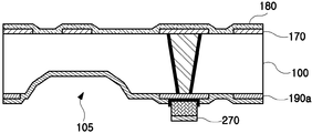
도 1h를 참조하면, 기판(100)의 제2면 상부에 도전 플러그(160)와 접속되는 상부 금속 배선(170)을 형성한다. 상부 금속 배선(170)은 약 0.5㎛ Au막(미도시)을 형성한 후 패터닝하여 형성하는 것이 바람직하다.Referring to FIG. 1H, an
도 1i를 참조하면, 상부 금속 배선(170) 및 기판(100)의 제2면을 도포하는 보호막인 상부 TEOS막(180)을 형성한다. 상부 TEOS막(180)은 약 500Å의 두께로 형성하는 것이 바람직하다.Referring to FIG. 1I, the
도 1j를 참조하면, 기판(100)의 제1면에 Au막(190)을 형성한다. Au막(190)은 약 0.5㎛의 두께로 형성하는 것이 바람직하다.Referring to FIG. 1J, an
도 1k를 참조하면, Au막(190)을 패터닝하여 도전 플러그(160)와 접속되는 하부 금속 배선(190a)을 형성한다. 다음에는, 하부 금속 배선(190a) 및 기판(100)의 제1면을 도포하는 보호막인 하부 TEOS막(200)을 형성한다.Referring to FIG. 1K, the
도 1l을 참조하면, 하부 TEOS막(200)을 선택적으로 식각하여 도전 플러그(160) 상부의 하부 금속 배선(190a) 표면을 노출시키는 제1 개구부(210)를 포함하는 하부 TEOS막 패턴(200a)을 형성한다.Referring to FIG. 1L, the lower
도 1m을 참조하면, 하부 TEOS막 패턴(200a) 및 제1 개구부(210)를 통하여 노출된 하부 금속 배선(190a)을 포함하는 전체 표면 상부에 씨드층(220)을 형성한다. 씨드층(220)은 Ti/Cu층으로 형성하는 것이 바람직하다. 더욱 바람직하게는, 씨드층(220)은 약 0.01㎛의 Ti층 및 약 0.2㎛의 Cu층의 적층 구조로 형성한다.Referring to FIG. 1M, the
다음에는, 전체 표면 상부에 제1 개구부(210)를 노출시키는 제2 개구부(240)를 포함하는 제1 마스크층 패턴(230)을 형성한다.Next, a first
도 1n을 참조하면, 제1 개구부(210) 및 제2 개구부(240)를 매립하는 제1 도전 범프(250)를 형성한다. 제1 도전 범프(250)는 도금 공정을 수행하여 기판(100)의 제1면 상부에 약 100㎛의 Ni-Co층(미도시)을 형성하고 제1 마스크층 패턴(230)이 노출될 때까지 CMP 공정 등의 연마 공정을 수행하여 형성하는 것이 바람직하다.Referring to FIG. 1N, a first
도 1o를 참조하면, 제1 도전 범프(250)를 노출시키는 제3 개구부(270)를 포함하는 제2 마스크층 패턴(260)을 형성한다.Referring to FIG. 1O, a second
도 1p를 참조하면, 제3 개구부(270)를 매립하는 제2 도전 범프(280)를 형성한다. 제2 도전 범프(280)는 도금 공정을 수행하여 기판(100)의 제1면 상부에 약 100㎛의 Ni-Co층(미도시)을 형성하고 제2 마스크층 패턴(260)이 노출될 때까지 CMP 공정 등의 연마 공정을 수행하여 형성하는 것이 바람직하다.Referring to FIG. 1P, a second
도 1q를 참조하면, 제2 마스크층 패턴(260), 제1 마스크층 패턴(230) 및 씨드층(220)을 제거하여 제1 도전 범프(250) 및 제2 도전 범프(280)의 적층구조로 이루어진 도전 범프(290)를 형성한다.Referring to FIG. 1Q, a stack structure of the first
도 1r을 참조하면, 하부 TEOS막 패턴(200a) 및 상부 TEOS막(180)을 제거한다.Referring to FIG. 1R, the lower
도 1s를 참조하면, 도전 범프(290)의 표면에 접착층 재료(300)를 형성한다. 접착층 재료(300)는 스크린 프린팅 공정을 이용하여 약 20㎛의 AuSn층으로 형성하는 것이 바람직하다.Referring to FIG. 1S, an
도 1t를 참조하면, 도전 범프(290) 상부면 이외 부분의 접착층 재료(300)를 제거하여 접착층(310)을 형성한다.Referring to FIG. 1T, the
도 1u를 참조하면, 기판(400)에 형성된 프로브 빔(410) 단부의 범프(420)를 접착층(310)을 매개로 도전 범프(290)와 접합한다.Referring to FIG. 1U, the
도 1v를 참조하면, 기판(400)을 제거하여 프로브 카드를 형성한다.Referring to FIG. 1V, the
도 2a 내지 도 2w는 본 발명의 제2 실시예에 따른 프로브 카드 제조 방법을 도시한 단면도들이다.2A to 2W are cross-sectional views illustrating a method of manufacturing a probe card according to a second exemplary embodiment of the present invention.
도 2a를 참조하면, 기판(100)을 준비한다. 기판(100)은 약 525㎛의 두께를 가지는 유리 기판인 것이 바람직하다.Referring to FIG. 2A, a
도 2b를 참조하면, 기판(100)의 제1면에 프로브 빔의 유동을 위한 트렌치를 정의하는 감광막 패턴(103)을 형성한다.Referring to FIG. 2B, a
도 2c를 참조하면, 감광막 패턴(103)을 식각 마스크로 기판(100)을 식각하여 트렌치(105)를 형성한다. 트렌치(105)는 샌드 블래스팅 공정을 수행하여 약 100㎛의 깊이로 형성하는 것이 바람직한다.Referring to FIG. 2C, the
도 2d를 참조하면, 기판(100)의 제2면 상부에 쓰루-홀 예정 영역을 노출시키는 감광막 패턴(110)을 형성한다.Referring to FIG. 2D, a
도 2e를 참조하면, 감광막 패턴(110)을 식각 마스크로 식각 공정을 수행하여 쓰루-홀(120)을 형성한다. 여기서, 상기 식각 공정은 샌드 블래스팅(sand blasting) 공정인 것이 바람직하다. 쓰루-홀(120)은 상부의 지름이 약 300㎛ 정도이고 하부 지름이 약 80㎛ 정도인 것이 바람직하다.Referring to FIG. 2E, the through-
도 2f를 참조하면, 감광막 패턴(110)을 제거한 후, 쓰루-홀(120) 표면 및 기판(100)의 제2면을 포함하는 전체 표면 상부에 씨드층(130)을 형성한다. 씨드층(130)은 Ti/Cu층으로 형성하는 것이 바람직하다. 더욱 바람직하게는, 씨드층(130)은 약 0.01㎛의 Ti층 및 약 1㎛의 Cu층의 적층 구조로 형성한다.Referring to FIG. 2F, after removing the
도 2g를 참조하면, 씨드층(130) 상부에 쓰루-홀(120)을 노출시키는 감광막 패턴(140)을 형성한다. 감광막 패턴(140)은 약 120㎛의 두께로 형성하는 것이 바람직하다.Referring to FIG. 2G, a
도 2h를 참조하면, 쓰루-홀(120)을 적어도 매립하는 금속층(150)을 형성한다. 금속층(150)은 도금 공정을 이용하여 Cu로 형성하는 것이 바람직하다.Referring to FIG. 2H, the
도 2i를 참조하면, 기판(100)이 노출될 때까지 평탄화 식각 공정을 수행하여 도전 플러그(160)를 형성한다. 상기 평탄화 식각 공정은 CMP(Chemical Mechanical Polishing) 공정인 것이 바람직하다.Referring to FIG. 2I, the planar etching process is performed until the
도 2j를 참조하면, 기판(100)의 제2면 상부에 도전 플러그(160)와 접속되는 상부 금속 배선(170)을 형성한다. 상부 금속 배선(170)은 약 0.5㎛ Au막(미도시)을 형성한 후 패터닝하여 형성하는 것이 바람직하다.Referring to FIG. 2J, an
도 2k를 참조하면, 상부 금속 배선(170) 및 기판(100)의 제2면을 도포하는 보호막인 상부 TEOS막(180)을 형성한다. 상부 TEOS막(180)은 약 500Å의 두께로 형 성하는 것이 바람직하다.Referring to FIG. 2K, an
도 2l을 참조하면, 트렌치(105)를 포함하는 기판(100)의 제1면에 Au막(190)을 형성한다. Au막(190)은 약 0.5㎛의 두께로 형성하는 것이 바람직하다.Referring to FIG. 2L, an
도 2m을 참조하면, Au막(190)을 패터닝하여 도전 플러그(160)와 접속되는 하부 금속 배선(190a)을 형성한다. 다음에는, 하부 금속 배선(190a) 및 기판(100)의 제1면을 도포하는 보호막인 하부 TEOS막(200)을 형성한다.Referring to FIG. 2M, the
도 2n을 참조하면, 하부 TEOS막(200)을 선택적으로 식각하여 도전 플러그(160) 상부의 하부 금속 배선(190a) 표면을 노출시키는 제1 개구부(210)를 포함하는 하부 TEOS막 패턴(200a)을 형성한다.Referring to FIG. 2N, the lower
도 2o를 참조하면, 하부 TEOS막 패턴(200a) 및 제1 개구부(210)를 통하여 노출된 하부 금속 배선(190a)을 포함하는 전체 표면 상부에 씨드층(220)을 형성한다. 씨드층(220)은 Ti/Cu층으로 형성하는 것이 바람직하다. 더욱 바람직하게는, 씨드층(220)은 약 0.01㎛의 Ti층 및 약 0.2㎛의 Cu층의 적층 구조로 형성한다.Referring to FIG. 2O, the
도 2p를 참조하면, 전체 표면 상부에 제1 개구부(210)를 노출시키는 제2 개구부(240)를 포함하는 마스크층 패턴(230)을 형성한다.Referring to FIG. 2P, a
도 2q를 참조하면, 제1 개구부(210) 및 제2 개구부(240)를 매립하는 도전 범프(250)를 형성한다. 도전 범프(250)는 도금 공정을 수행하여 기판(100)의 제1면 상부에 약 100㎛의 Ni-Co층(미도시)을 형성하고 마스크층 패턴(230)이 노출될 때까지 CMP 공정 등의 연마 공정을 수행하여 형성하는 것이 바람직하다.Referring to FIG. 2Q, a
도 2r을 참조하면, 마스크층 패턴(230) 및 씨드층(220)을 제거한다.Referring to FIG. 2R, the
도 2s를 참조하면, 하부 TEOS막 패턴(200a) 및 상부 TEOS막(180)을 제거한다.Referring to FIG. 2S, the lower
도 2t를 참조하면, 도전 범프(250)의 표면에 접착층 재료(260)를 형성한다. 접착층 재료(260)는 스크린 프린팅 공정을 이용하여 약 20㎛의 AuSn층으로 형성하는 것이 바람직하다.Referring to FIG. 2T, an
도 2u를 참조하면, 도전 범프(250) 상부면 이외 부분의 접착층 재료(260)를 제거하여 접착층(270)을 형성한다.Referring to FIG. 2U, the
도 2v를 참조하면, 기판(300)에 형성된 프로브 빔(310) 단부의 범프(320)를 접착층(270)을 매개로 도전 범프(250)와 접합한다.Referring to FIG. 2V, the
도 2w를 참조하면, 기판(300)을 제거하여 프로브 카드를 형성한다.Referring to FIG. 2W, the
도 3a 내지 도 3i는 본 발명의 제3 실시예에 따른 프로브 카드 제조 방법을 도시한 단면도들이다.3A to 3I are cross-sectional views illustrating a method of manufacturing a probe card according to a third exemplary embodiment of the present invention.
도 3a를 참조하면, 제1 기판(100)의 제1면 및 제2면에 박막(110a, 110b)을 형성한다. 기판은 유리 기판인 것이 바람직하며, 박막(110a, 110b)은 폴리실리콘층, 금속층 및 실리콘층 중 어느 하나로 형성하는 것이 바람직하다.Referring to FIG. 3A,
도 3b를 참조하면, 제1 기판(100)의 제1면을 선택적으로 식각하여 프로브 빔의 유동을 위한 트렌치(120)를 형성한다.Referring to FIG. 3B, the first surface of the
도 3c를 참조하면, 제1 기판(100)의 제2면 상부에 쓰루-홀 예정 영역을 노출시키는 감광막 패턴(130)을 형성한다.Referring to FIG. 3C, a
도 3d를 참조하면, 감광막 패턴(130)을 식각 마스크로 제1 기판(100)을 식각 하여 쓰루-홀(140)을 형성한다. 여기서, 상기 식각 공정은 샌드 블래스팅 공정 또는 레이저 드릴링 공정인 것이 바람직하다.Referring to FIG. 3D, the
도 3e를 참조하면, 박막(110a, 110b) 및 감광막 패턴(130)을 제거한다. 상기 제거 공정은 제1 기판(100)이 노출될 때까지 연마하는 공정, 예를 들면 그라인딩(grinding), 폴리싱(poilishing) 또는 CMP 공정으로 수행하는 것이 바람직하다.Referring to FIG. 3E, the
도 3f를 참조하면, 프로브 빔(210)이 형성된 제2 기판(200)의 상부에 씨드층(220)을 형성한다.Referring to FIG. 3F, the
도 3g를 참조하면, 프로브 빔의 단부에 쓰루-홀(140)을 정렬하고, 프로브 빔(210)이 형성된 제2 기판(200)을 제1 기판(100)과 접합한다. 상기 접합 공정은 양성 접합(anodic bonding) 공정인 것이 바람직하다.Referring to FIG. 3G, the through-
도 3h를 참조하면, 쓰루-홀(140)을 매립하는 도전 플러그(230)를 형성한다.Referring to FIG. 3H, the
도 3i를 참조하면, 제2 기판(200)을 제거하여 프로브 카드를 형성한다. 상기 제거 공정은 KOH 용액 또는 TMAH(Tetra-methyl ammonium hydroxide) 용액을 사용하여 수행되는 것이 바람직하다.Referring to FIG. 3I, the
본 발명에 따른 프로브 카드 제조 방법은 스페이스 트랜스포머(space transformer)와 프로브 빔 사이에 쓰루-홀을 매립하는 도전 플러그를 구비한 기판을 추가함으로써 열특성이 우수하며, 리페어가 가능하고 프로브 카드의 피치(pitch)를 용이하게 감소시킬 수 있다는 장점이 있다.The method of manufacturing a probe card according to the present invention is excellent in thermal characteristics by adding a substrate having a conductive plug for embedding a through-hole between a space transformer and a probe beam, which enables repair and a pitch of the probe card ( Pitch) can be easily reduced.
Claims (32)
Priority Applications (1)
| Application Number | Priority Date | Filing Date | Title |
|---|---|---|---|
| KR1020060054339A KR100745373B1 (en) | 2006-06-16 | 2006-06-16 | Probe card manufacturing method |
Applications Claiming Priority (1)
| Application Number | Priority Date | Filing Date | Title |
|---|---|---|---|
| KR1020060054339A KR100745373B1 (en) | 2006-06-16 | 2006-06-16 | Probe card manufacturing method |
Publications (1)
| Publication Number | Publication Date |
|---|---|
| KR100745373B1 true KR100745373B1 (en) | 2007-08-02 |
Family
ID=38601676
Family Applications (1)
| Application Number | Title | Priority Date | Filing Date |
|---|---|---|---|
| KR1020060054339A Expired - Fee Related KR100745373B1 (en) | 2006-06-16 | 2006-06-16 | Probe card manufacturing method |
Country Status (1)
| Country | Link |
|---|---|
| KR (1) | KR100745373B1 (en) |
Cited By (6)
| Publication number | Priority date | Publication date | Assignee | Title |
|---|---|---|---|---|
| KR100806383B1 (en) | 2007-01-05 | 2008-02-27 | 세크론 주식회사 | Probe card manufacturing method |
| KR100840765B1 (en) | 2007-01-09 | 2008-06-24 | 김복곤 | Cantilever type probe manufacturing method |
| KR100891025B1 (en) * | 2007-08-27 | 2009-04-02 | (주)미코엠에스티 | Probe card structure and its formation method |
| KR100928901B1 (en) | 2007-09-04 | 2009-11-30 | 윌테크놀러지(주) | Probe card manufacturing method |
| KR101415635B1 (en) | 2012-12-28 | 2014-07-04 | (재)한국나노기술원 | Manufacturing method of space transformer for glass base probe card and the space transformer for glass base probe card thereby |
| KR101441632B1 (en) * | 2012-12-28 | 2014-09-23 | (재)한국나노기술원 | Manufacturing method of space transformer for glass base probe card and the space transformer for glass base probe card thereby |
Citations (4)
| Publication number | Priority date | Publication date | Assignee | Title |
|---|---|---|---|---|
| JPH1038924A (en) | 1996-07-25 | 1998-02-13 | Advantest Corp | Probe card |
| KR20020011286A (en) * | 2000-08-01 | 2002-02-08 | 이재혁 | Semiconductor Probe Device and Semiconductor Probe Chip Using the Same, and Fabricating Method thereof |
| JP2004133128A (en) | 2002-10-09 | 2004-04-30 | Ricoh Co Ltd | Developing roller, developing device, process cartridge, and image forming apparatus |
| KR20060027423A (en) * | 2004-09-22 | 2006-03-28 | 주식회사 파이컴 | Method for manufacturing vertical electrical contactor and thus vertical electrical contactor |
-
2006
- 2006-06-16 KR KR1020060054339A patent/KR100745373B1/en not_active Expired - Fee Related
Patent Citations (4)
| Publication number | Priority date | Publication date | Assignee | Title |
|---|---|---|---|---|
| JPH1038924A (en) | 1996-07-25 | 1998-02-13 | Advantest Corp | Probe card |
| KR20020011286A (en) * | 2000-08-01 | 2002-02-08 | 이재혁 | Semiconductor Probe Device and Semiconductor Probe Chip Using the Same, and Fabricating Method thereof |
| JP2004133128A (en) | 2002-10-09 | 2004-04-30 | Ricoh Co Ltd | Developing roller, developing device, process cartridge, and image forming apparatus |
| KR20060027423A (en) * | 2004-09-22 | 2006-03-28 | 주식회사 파이컴 | Method for manufacturing vertical electrical contactor and thus vertical electrical contactor |
Cited By (6)
| Publication number | Priority date | Publication date | Assignee | Title |
|---|---|---|---|---|
| KR100806383B1 (en) | 2007-01-05 | 2008-02-27 | 세크론 주식회사 | Probe card manufacturing method |
| KR100840765B1 (en) | 2007-01-09 | 2008-06-24 | 김복곤 | Cantilever type probe manufacturing method |
| KR100891025B1 (en) * | 2007-08-27 | 2009-04-02 | (주)미코엠에스티 | Probe card structure and its formation method |
| KR100928901B1 (en) | 2007-09-04 | 2009-11-30 | 윌테크놀러지(주) | Probe card manufacturing method |
| KR101415635B1 (en) | 2012-12-28 | 2014-07-04 | (재)한국나노기술원 | Manufacturing method of space transformer for glass base probe card and the space transformer for glass base probe card thereby |
| KR101441632B1 (en) * | 2012-12-28 | 2014-09-23 | (재)한국나노기술원 | Manufacturing method of space transformer for glass base probe card and the space transformer for glass base probe card thereby |
Similar Documents
| Publication | Publication Date | Title |
|---|---|---|
| US8272124B2 (en) | Anchoring carbon nanotube columns | |
| US7685705B2 (en) | Method of fabricating a probe card | |
| US7409762B2 (en) | Method for fabricating an interconnect for semiconductor components | |
| JP2009540291A (en) | Cantilever type probe manufacturing method and probe card manufacturing method using the same | |
| KR100523745B1 (en) | Microprobe and Method for Manufacturing the Same Using MEMS and Electroplating Technology | |
| JP2009524800A (en) | Probe array structure and manufacturing method of probe array structure | |
| KR100473584B1 (en) | Cantilever-type probe card and method for manufacturing the same using silicon micromachining technology | |
| KR100745373B1 (en) | Probe card manufacturing method | |
| JP2008089461A (en) | Prober for semiconductor integrated circuit inspection | |
| US20080074127A1 (en) | Probe substrate for test and manufacturing method thereof | |
| KR100796204B1 (en) | Method for manufacturing cantilever structure of probe card | |
| KR100796207B1 (en) | Method for manufacturing probe structure of probe card | |
| KR100977166B1 (en) | Needle Probe Manufacturing Method | |
| KR101149808B1 (en) | Manufacturing method for probe and probe card | |
| KR100806380B1 (en) | Probe card manufacturing method and probe card thereby | |
| KR100736776B1 (en) | Method for manufacturing contact element for probe card and contact element for probe card manufactured therefrom | |
| KR100585561B1 (en) | Vertical Electrical Contact and Manufacturing Method Thereof | |
| KR100733815B1 (en) | Probe Structure Manufacturing Method | |
| KR101322264B1 (en) | Electronical contact element production method for probe card | |
| KR101273970B1 (en) | Method of Manufacturing Probe Needle and Probe | |
| KR100915326B1 (en) | Method of manufacturing an apparatus for inspecting electric condition | |
| US7685704B2 (en) | Method for manufacturing bump of probe card | |
| KR101329811B1 (en) | Electronical contact element production method for probe card | |
| Lim et al. | Highly Productive Process Technologies of Cantilevertype Microprobe Arrays for Wafer Level Chip Testing | |
| KR101242001B1 (en) | Probe Structure Manufacturing Method |
Legal Events
| Date | Code | Title | Description |
|---|---|---|---|
| A201 | Request for examination | ||
| PA0109 | Patent application |
St.27 status event code: A-0-1-A10-A12-nap-PA0109 |
|
| PA0201 | Request for examination |
St.27 status event code: A-1-2-D10-D11-exm-PA0201 |
|
| R17-X000 | Change to representative recorded |
St.27 status event code: A-3-3-R10-R17-oth-X000 |
|
| R18-X000 | Changes to party contact information recorded |
St.27 status event code: A-3-3-R10-R18-oth-X000 |
|
| D13-X000 | Search requested |
St.27 status event code: A-1-2-D10-D13-srh-X000 |
|
| D14-X000 | Search report completed |
St.27 status event code: A-1-2-D10-D14-srh-X000 |
|
| E902 | Notification of reason for refusal | ||
| PE0902 | Notice of grounds for rejection |
St.27 status event code: A-1-2-D10-D21-exm-PE0902 |
|
| R17-X000 | Change to representative recorded |
St.27 status event code: A-3-3-R10-R17-oth-X000 |
|
| P11-X000 | Amendment of application requested |
St.27 status event code: A-2-2-P10-P11-nap-X000 |
|
| P13-X000 | Application amended |
St.27 status event code: A-2-2-P10-P13-nap-X000 |
|
| E701 | Decision to grant or registration of patent right | ||
| PE0701 | Decision of registration |
St.27 status event code: A-1-2-D10-D22-exm-PE0701 |
|
| GRNT | Written decision to grant | ||
| PR0701 | Registration of establishment |
St.27 status event code: A-2-4-F10-F11-exm-PR0701 |
|
| PR1002 | Payment of registration fee |
St.27 status event code: A-2-2-U10-U11-oth-PR1002 Fee payment year number: 1 |
|
| PG1601 | Publication of registration |
St.27 status event code: A-4-4-Q10-Q13-nap-PG1601 |
|
| R18-X000 | Changes to party contact information recorded |
St.27 status event code: A-5-5-R10-R18-oth-X000 |
|
| PN2301 | Change of applicant |
St.27 status event code: A-5-5-R10-R11-asn-PN2301 |
|
| PN2301 | Change of applicant |
St.27 status event code: A-5-5-R10-R14-asn-PN2301 |
|
| P14-X000 | Amendment of ip right document requested |
St.27 status event code: A-5-5-P10-P14-nap-X000 |
|
| P16-X000 | Ip right document amended |
St.27 status event code: A-5-5-P10-P16-nap-X000 |
|
| Q16-X000 | A copy of ip right certificate issued |
St.27 status event code: A-4-4-Q10-Q16-nap-X000 |
|
| PR1001 | Payment of annual fee |
St.27 status event code: A-4-4-U10-U11-oth-PR1001 Fee payment year number: 4 |
|
| PR1001 | Payment of annual fee |
St.27 status event code: A-4-4-U10-U11-oth-PR1001 Fee payment year number: 5 |
|
| FPAY | Annual fee payment |
Payment date: 20120725 Year of fee payment: 6 |
|
| PR1001 | Payment of annual fee |
St.27 status event code: A-4-4-U10-U11-oth-PR1001 Fee payment year number: 6 |
|
| FPAY | Annual fee payment |
Payment date: 20130725 Year of fee payment: 7 |
|
| PR1001 | Payment of annual fee |
St.27 status event code: A-4-4-U10-U11-oth-PR1001 Fee payment year number: 7 |
|
| R18-X000 | Changes to party contact information recorded |
St.27 status event code: A-5-5-R10-R18-oth-X000 |
|
| FPAY | Annual fee payment |
Payment date: 20140725 Year of fee payment: 8 |
|
| PR1001 | Payment of annual fee |
St.27 status event code: A-4-4-U10-U11-oth-PR1001 Fee payment year number: 8 |
|
| FPAY | Annual fee payment |
Payment date: 20150622 Year of fee payment: 9 |
|
| PR1001 | Payment of annual fee |
St.27 status event code: A-4-4-U10-U11-oth-PR1001 Fee payment year number: 9 |
|
| P14-X000 | Amendment of ip right document requested |
St.27 status event code: A-5-5-P10-P14-nap-X000 |
|
| FPAY | Annual fee payment |
Payment date: 20160704 Year of fee payment: 10 |
|
| PR1001 | Payment of annual fee |
St.27 status event code: A-4-4-U10-U11-oth-PR1001 Fee payment year number: 10 |
|
| P14-X000 | Amendment of ip right document requested |
St.27 status event code: A-5-5-P10-P14-nap-X000 |
|
| PN2301 | Change of applicant |
St.27 status event code: A-5-5-R10-R13-asn-PN2301 St.27 status event code: A-5-5-R10-R11-asn-PN2301 |
|
| LAPS | Lapse due to unpaid annual fee | ||
| PC1903 | Unpaid annual fee |
St.27 status event code: A-4-4-U10-U13-oth-PC1903 Not in force date: 20170728 Payment event data comment text: Termination Category : DEFAULT_OF_REGISTRATION_FEE |
|
| P22-X000 | Classification modified |
St.27 status event code: A-4-4-P10-P22-nap-X000 |
|
| PC1903 | Unpaid annual fee |
St.27 status event code: N-4-6-H10-H13-oth-PC1903 Ip right cessation event data comment text: Termination Category : DEFAULT_OF_REGISTRATION_FEE Not in force date: 20170728 |
|
| P22-X000 | Classification modified |
St.27 status event code: A-4-4-P10-P22-nap-X000 |