KR100741076B1 - Organic light emitting display - Google Patents
Organic light emitting display Download PDFInfo
- Publication number
- KR100741076B1 KR100741076B1 KR1020050039232A KR20050039232A KR100741076B1 KR 100741076 B1 KR100741076 B1 KR 100741076B1 KR 1020050039232 A KR1020050039232 A KR 1020050039232A KR 20050039232 A KR20050039232 A KR 20050039232A KR 100741076 B1 KR100741076 B1 KR 100741076B1
- Authority
- KR
- South Korea
- Prior art keywords
- transistor
- light emitting
- organic light
- capacitor
- voltage
- Prior art date
- Legal status (The legal status is an assumption and is not a legal conclusion. Google has not performed a legal analysis and makes no representation as to the accuracy of the status listed.)
- Expired - Fee Related
Links
Images


Classifications
-
- G—PHYSICS
- G09—EDUCATION; CRYPTOGRAPHY; DISPLAY; ADVERTISING; SEALS
- G09G—ARRANGEMENTS OR CIRCUITS FOR CONTROL OF INDICATING DEVICES USING STATIC MEANS TO PRESENT VARIABLE INFORMATION
- G09G3/00—Control arrangements or circuits, of interest only in connection with visual indicators other than cathode-ray tubes
- G09G3/20—Control arrangements or circuits, of interest only in connection with visual indicators other than cathode-ray tubes for presentation of an assembly of a number of characters, e.g. a page, by composing the assembly by combination of individual elements arranged in a matrix no fixed position being assigned to or needed to be assigned to the individual characters or partial characters
- G09G3/22—Control arrangements or circuits, of interest only in connection with visual indicators other than cathode-ray tubes for presentation of an assembly of a number of characters, e.g. a page, by composing the assembly by combination of individual elements arranged in a matrix no fixed position being assigned to or needed to be assigned to the individual characters or partial characters using controlled light sources
- G09G3/30—Control arrangements or circuits, of interest only in connection with visual indicators other than cathode-ray tubes for presentation of an assembly of a number of characters, e.g. a page, by composing the assembly by combination of individual elements arranged in a matrix no fixed position being assigned to or needed to be assigned to the individual characters or partial characters using controlled light sources using electroluminescent panels
- G09G3/32—Control arrangements or circuits, of interest only in connection with visual indicators other than cathode-ray tubes for presentation of an assembly of a number of characters, e.g. a page, by composing the assembly by combination of individual elements arranged in a matrix no fixed position being assigned to or needed to be assigned to the individual characters or partial characters using controlled light sources using electroluminescent panels semiconductive, e.g. using light-emitting diodes [LED]
- G09G3/3208—Control arrangements or circuits, of interest only in connection with visual indicators other than cathode-ray tubes for presentation of an assembly of a number of characters, e.g. a page, by composing the assembly by combination of individual elements arranged in a matrix no fixed position being assigned to or needed to be assigned to the individual characters or partial characters using controlled light sources using electroluminescent panels semiconductive, e.g. using light-emitting diodes [LED] organic, e.g. using organic light-emitting diodes [OLED]
- G09G3/3225—Control arrangements or circuits, of interest only in connection with visual indicators other than cathode-ray tubes for presentation of an assembly of a number of characters, e.g. a page, by composing the assembly by combination of individual elements arranged in a matrix no fixed position being assigned to or needed to be assigned to the individual characters or partial characters using controlled light sources using electroluminescent panels semiconductive, e.g. using light-emitting diodes [LED] organic, e.g. using organic light-emitting diodes [OLED] using an active matrix
- G09G3/3233—Control arrangements or circuits, of interest only in connection with visual indicators other than cathode-ray tubes for presentation of an assembly of a number of characters, e.g. a page, by composing the assembly by combination of individual elements arranged in a matrix no fixed position being assigned to or needed to be assigned to the individual characters or partial characters using controlled light sources using electroluminescent panels semiconductive, e.g. using light-emitting diodes [LED] organic, e.g. using organic light-emitting diodes [OLED] using an active matrix with pixel circuitry controlling the current through the light-emitting element
- G09G3/3241—Control arrangements or circuits, of interest only in connection with visual indicators other than cathode-ray tubes for presentation of an assembly of a number of characters, e.g. a page, by composing the assembly by combination of individual elements arranged in a matrix no fixed position being assigned to or needed to be assigned to the individual characters or partial characters using controlled light sources using electroluminescent panels semiconductive, e.g. using light-emitting diodes [LED] organic, e.g. using organic light-emitting diodes [OLED] using an active matrix with pixel circuitry controlling the current through the light-emitting element the current through the light-emitting element being set using a data current provided by the data driver, e.g. by using a two-transistor current mirror
- G09G3/325—Control arrangements or circuits, of interest only in connection with visual indicators other than cathode-ray tubes for presentation of an assembly of a number of characters, e.g. a page, by composing the assembly by combination of individual elements arranged in a matrix no fixed position being assigned to or needed to be assigned to the individual characters or partial characters using controlled light sources using electroluminescent panels semiconductive, e.g. using light-emitting diodes [LED] organic, e.g. using organic light-emitting diodes [OLED] using an active matrix with pixel circuitry controlling the current through the light-emitting element the current through the light-emitting element being set using a data current provided by the data driver, e.g. by using a two-transistor current mirror the data current flowing through the driving transistor during a setting phase, e.g. by using a switch for connecting the driving transistor to the data driver
-
- G—PHYSICS
- G09—EDUCATION; CRYPTOGRAPHY; DISPLAY; ADVERTISING; SEALS
- G09G—ARRANGEMENTS OR CIRCUITS FOR CONTROL OF INDICATING DEVICES USING STATIC MEANS TO PRESENT VARIABLE INFORMATION
- G09G2300/00—Aspects of the constitution of display devices
- G09G2300/04—Structural and physical details of display devices
- G09G2300/0421—Structural details of the set of electrodes
- G09G2300/043—Compensation electrodes or other additional electrodes in matrix displays related to distortions or compensation signals, e.g. for modifying TFT threshold voltage in column driver
-
- G—PHYSICS
- G09—EDUCATION; CRYPTOGRAPHY; DISPLAY; ADVERTISING; SEALS
- G09G—ARRANGEMENTS OR CIRCUITS FOR CONTROL OF INDICATING DEVICES USING STATIC MEANS TO PRESENT VARIABLE INFORMATION
- G09G2320/00—Control of display operating conditions
- G09G2320/02—Improving the quality of display appearance
- G09G2320/0233—Improving the luminance or brightness uniformity across the screen
Landscapes
- Engineering & Computer Science (AREA)
- Physics & Mathematics (AREA)
- Computer Hardware Design (AREA)
- General Physics & Mathematics (AREA)
- Theoretical Computer Science (AREA)
- Electroluminescent Light Sources (AREA)
- Control Of Indicators Other Than Cathode Ray Tubes (AREA)
- Control Of El Displays (AREA)
Abstract
본 발명은 구동 트랜지스터의 문턱 전압의 편차를 보상하여 균일한 휘도를 표현하고, 스위칭 트랜지스터의 킥 백(Kick_back) 현상에 의해 발생하는 구동 전압의 변화를 최소화하여 고해상도 구현이 가능한 유기 발광 표시 장치를 개시한다. 유기 발광 표시 장치는 유기 발광 소자, 제1 내지 제4 트랜지스터, 제1 캐패시터 및 저장소자를 포함한다. 유기 발광 소자는 인가되는 전류에 의해 대응하여 빛을 방출한다. 제1 트랜지스터는 유기 발광소자로 구동전류를 공급하고, 제2 트랜지스터는 선택신호에 응답하여 스위칭 되어, 제1 트랜지스터로의 데이터 신호의 전달을 제어한다. 제3 트랜지스터는 제1 트랜지스터를 다이오드 연결시키고, 제4 트랜지스터는 제1 트랜지스터와 유기 발광 소자 사이에 개재되고, 제2 발광제어 신호에 응답하여 유기 발광소자로 공급되는 구동전류를 스위칭 한다. 제1 캐패시터는 제1 트랜지스터의 구동전류에 대응하는 전압을 저장하고, 저장소자는 제1 캐패시터 및 제4 트랜지스터 사이에 개재되고, 제3 트랜지스터 온/오프 시에 발생하는 누설전류의 일부를 저장한다.The present invention discloses an organic light emitting display device capable of high resolution by compensating for variation in threshold voltage of a driving transistor to express uniform luminance and minimizing a change in driving voltage caused by a kick back phenomenon of a switching transistor. do. The organic light emitting diode display includes an organic light emitting diode, first to fourth transistors, a first capacitor, and a reservoir. The organic light emitting element emits light correspondingly by the applied current. The first transistor supplies a driving current to the organic light emitting element, and the second transistor is switched in response to the selection signal to control the transfer of the data signal to the first transistor. The third transistor diode-connects the first transistor, and the fourth transistor is interposed between the first transistor and the organic light emitting element, and switches the driving current supplied to the organic light emitting element in response to the second light emission control signal. The first capacitor stores a voltage corresponding to the driving current of the first transistor, and the reservoir is interposed between the first capacitor and the fourth transistor, and stores a part of the leakage current generated when the third transistor is turned on / off.
Description
본 발명의 상세한 설명에서 인용되는 도면을 보다 충분히 이해하기 위하여 각 도면의 간단한 설명이 제공된다.BRIEF DESCRIPTION OF THE DRAWINGS In order to better understand the drawings cited in the detailed description of the invention, a brief description of each drawing is provided.
도 1은 종래의 유기 발광 표시장치를 나타내는 개략도이다. 1 is a schematic diagram illustrating a conventional organic light emitting display device.
도 2는 도 1의 유기 발광 표시장치에 채용된 화소의 회로도이다. FIG. 2 is a circuit diagram of a pixel employed in the OLED display of FIG. 1.
도 3은 본 발명의 제1 실시 예에 따른 문턱 전압 보상을 위한 화소 회로도이다.3 is a pixel circuit diagram for threshold voltage compensation according to a first embodiment of the present invention.
도 4는 도 3에 도시된 화소 회로를 구동하기 위한 구동 파형도 이다.FIG. 4 is a driving waveform diagram for driving the pixel circuit shown in FIG. 3.
도 5는 도 3의 화소 회로 중 제3 트랜지스터(M3)가 턴-오프 되는 순간 발생하는 데이터 전압 변동을 설명하기 위한 도면이다.FIG. 5 is a diagram for describing a data voltage variation occurring when a third transistor M3 is turned off in the pixel circuit of FIG. 3.
도 6은 본 발명의 제2 실시 예에 따른 킥-백 현상을 보상하기 위한 화소 회로도이다.6 is a pixel circuit diagram to compensate for a kick-back phenomenon according to a second embodiment of the present invention.
도 7은 도 6에 도시된 화소 회로를 구동하기 위한 구동 파형도 이다.FIG. 7 is a driving waveform diagram for driving the pixel circuit shown in FIG. 6.
도 8은 도 6의 화소 회로 중 제3 트랜지스터(M3)가 턴-오프 되는 순간 발생하는 데이터 전압 변동을 설명하기 위한 도면이다.FIG. 8 is a view for explaining a data voltage variation occurring when the third transistor M3 is turned off in the pixel circuit of FIG. 6.
도 9는 본 발명의 제3 실시 예에 따른 킥-백 현상을 보상하기 위한 화소 회로도이다.9 is a pixel circuit diagram to compensate for a kick-back phenomenon according to a third exemplary embodiment of the present invention.
본 발명은 유기 발광 표시 장치에 관한 것으로, 더욱 상세하게는 화소 회로에 포함된 구동 트랜지스터의 문턱 전압의 편차를 보상하여 균일한 휘도를 표현하고, 스위칭 트랜지스터의 킥 백(Kick_back) 현상에 의해 발생하는 구동 전압의 변화를 최소화하여 고해상도 구현이 가능한 유기 발광 표시 장치에 관한 것이다.BACKGROUND OF THE
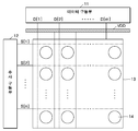
도 1은 종래의 유기 발광 표시장치를 나타낸다. 1 illustrates a conventional organic light emitting display device.
도 1에 도시된 바와 같이, 상기 유기 발광 표시장치(10)는, 데이터 구동부(11), 주사 구동부(12) 및 표시부(13)를 구비한다. 상기 표시부(13)에는 세로 방향으로 뻗어있는 복수의 데이터 신호선, 가로로 뻗어있는 복수의 선택 신호선이 포함된다. As shown in FIG. 1, the organic light emitting diode display 10 includes a
또한, 상기 유기 발광 표시장치의 표시부(13) 에는, 상기 데이터 신호선 및 선택신호선에 의해 매트릭스 형태로 화소(14)가 정의되며, 상기 화소(14)에는 화소회로가 형성되어 있다.In the
데이터 구동부(11)는 데이터 신호선들을 통하여 데이터 신호(D[1] 내지 D[m])를 화소회로에 전달한다. 주사 구동부(12)는 선택 신호 선들을 통하여 선택신호(S[1] 내지 S[n])를 인가하여, 표시부(13)를 구성하는 복수 개의 화소(14)들을 라인 단위로 선택한다. 상기 선택신호(S[1] 내지 S[n])에 의하여 선택된 화소(14)들에는 데이터 신호(D[1] 내지 D[m])의 정보가 전달된다. 한편, 소정의 전원전압 (VDD)이 버스라인을 통해 상기 표시부(13)의 모든 화소(14)들로 공급된다. The
한편, 도 2는 도 1의 유기 발광 표시장치에 채용된 화소의 회로도이다.2 is a circuit diagram of a pixel employed in the OLED display of FIG. 1.
도 2를 참조하면, 유기 발광 표시장치의 화소는 유기 발광 소자(OLED) 및 두 개의 트랜지스터(M1, M2)와 하나의 캐패시터(Cst))를 구비하며, 일반적으로 상기 제1 및 제2 트랜지스터(M1, M2)는 박막 트랜지스터(TFT)가 사용된다.Referring to FIG. 2, a pixel of an organic light emitting diode display includes an organic light emitting diode OLED, two transistors M1 and M2, and one capacitor C st , and are generally the first and second transistors. Thin film transistors TFT are used for M1 and M2.
상기 도 2의 화소회로에서는 제1 트랜지스터(M1)의 제1전극이 데이터 신호선에 연결된다. 이때 주전극에 인가되는 선택신호(S[n])에 의하여 상기 제1 트랜지스터(M1)가 온 되어짐으로써, 데이터 신호(D[m])가 화소회로로 인가된다.In the pixel circuit of FIG. 2, the first electrode of the first transistor M1 is connected to the data signal line. At this time, the first transistor M1 is turned on by the selection signal S [n] applied to the main electrode, so that the data signal D [m] is applied to the pixel circuit.
한편, 상기 캐패시터(Cst)는 제2 트랜지스터(M2)의 제1전극과 주전극 사이에 연결되어, 데이터 전압을 일정 기간 유지한다. 또한, 상기 제2 트랜지스터(M2)는 캐패시터(Cst)의 양 전극 사이에 걸린 전압에 대응하는 전류를 상기 유기 발광 소자(OLED)로 공급한다. Meanwhile, the capacitor C st is connected between the first electrode and the main electrode of the second transistor M2 to maintain the data voltage for a predetermined period. In addition, the second transistor M2 supplies a current corresponding to the voltage applied between both electrodes of the capacitor C st to the organic light emitting diode OLED.
상기 제1 트랜지스터(M1)가 온 되어지면, 데이터 신호선을 통해 인가된 데이터 전압이 캐패시터(Cst)에 저장되며, 이후 제1 트랜지스터(M1)가 오프 되어지는 경우에도 상기 캐패시터(Cst)에 저장된 데이터 전압에 대응하는 전류가 제2 트랜지스터(M2)를 통해 유기 발광 소자(OLED)로 인가된다. 이에 따라 제1 트랜지스터(M1)가 오프된 경우에도 상기 유기 발광 소자(OLED)는 소정의 기간동안 발광을 유지하게 된다. When the first transistor M1 is turned on, the data voltage applied through the data signal line is stored in the capacitor C st , and thereafter, even when the first transistor M1 is turned off, the capacitor C st is applied to the capacitor C st . A current corresponding to the stored data voltage is applied to the organic light emitting diode OLED through the second transistor M2. Accordingly, the organic light emitting diode OLED maintains light emission for a predetermined period even when the first transistor M1 is turned off.
이때, 유기 발광 소자(OLED)에 흐르는 전류는 다음의 수학식 1과 같다. At this time, the current flowing through the OLED is represented by
[수학식 1][Equation 1]
![]()
![]()
![]()
![]()
![]()
![]()
상기 수학식 1에서, ![]()
![]()
그러나, 상기와 같은 전압 기입 방식의 화소회로에서는, 제2 트랜지스터와 같은 구동 트랜지스터가 그 제조 공정 상 문턱전압(Vth)의 편차가 발생함으로써, 균일한 밝기의 화면을 얻기 어려운 문제점이 발생한다. 즉, 소정의 구동 트랜지스터가 높은 문턱전압의 절대값을 갖는 경우, 상기 수학식 1에 언급한 바와 같이 ![]()
![]()
![]()
![]()
본 발명이 이루고자 하는 기술적인 과제는 화소 회로에 포함된 구동 트랜지스터의 문턱 전압의 편차를 보상하여 균일한 휘도를 표현할 수 있는 유기 발광 표시 장치를 제공하는데 있다.SUMMARY OF THE INVENTION The present invention has been made in an effort to provide an organic light emitting display device capable of expressing uniform luminance by compensating for variations in threshold voltages of driving transistors included in a pixel circuit.
본 발명이 이루고자 하는 다른 기술적 과제는 킥 백(Kick_back) 현상에 의해 발생하는 구동 전압의 변화를 최소화하여 고해상도 구현이 가능한 유기 발광 표시 장치를 제공하는데 있다.Another object of the present invention is to provide an organic light emitting display device capable of high resolution by minimizing a change in driving voltage caused by a kick back phenomenon.
본 발명이 이루고자 하는 기술적인 과제를 해결하기 위한 본 발명에 따른 유기 발광 표시 장치는 인가되는 전류에 의해 대응하여 빛을 방출하는 유기 발광 소자; 상기 유기 발광 소자로 구동전류를 공급하는 제1 트랜지스터; 선택신호에 응답하여 스위칭 되어, 상기 제1 트랜지스터로의 데이터 신호의 전달을 제어하는 제2 트랜지스터; 상기 제1 트랜지스터를 다이오드 연결시키는 제3 트랜지스터; 상기 제1 트랜지스터와 상기 유기 발광 소자 사이에 개재되고, 제2 발광제어 신호에 응답하여 상기 유기 발광소자로 공급되는 구동전류를 스위칭하는 제4 트랜지스터; 및 상기 제1 트랜지스터의 구동전류에 대응하는 전압을 저장하는 제1 캐패시터를 포함하는 것이 바람직하다.According to an aspect of the present invention, there is provided an organic light emitting display device including: an organic light emitting device that emits light in response to an applied current; A first transistor supplying a driving current to the organic light emitting element; A second transistor switched in response to a selection signal to control transmission of a data signal to the first transistor; A third transistor for diode-connecting the first transistor; A fourth transistor interposed between the first transistor and the organic light emitting element and switching a driving current supplied to the organic light emitting element in response to a second light emission control signal; And a first capacitor configured to store a voltage corresponding to the driving current of the first transistor.
본 발명이 이루고자 하는 다른 기술적 과제를 해결하기 위한 본 발명에 따른 유기 발광 표시장치는 인가되는 전류에 의해 대응하여 빛을 방출하는 유기 발광 소자; 상기 유기 발광 소자로 구동전류를 공급하는 제1 트랜지스터; 선택신호에 응답하여 스위칭 되어, 상기 제1 트랜지스터로의 데이터 신호의 전달을 제어하는 제2 트랜지스터; 상기 제1 트랜지스터를 다이오드 연결시키는 제3 트랜지스터; 상기 제1 트랜지스터와 상기 유기 발광 소자 사이에 개재되고, 제2 발광제어 신호에 응답하여 상기 유기 발광소자로 공급되는 구동전류를 스위칭하는 제4 트랜지스터; 상기 제1 트랜지스터의 구동전류에 대응하는 전압을 저장하는 제1 캐패시터; 및 상기 제 1 캐패시터 및 제4 트랜지스터 사이에 개재되고, 상기 제3 트랜지스터 온/오프 시에 발생하는 누설전류의 일부를 저장하는 저장소자를 포함하는 것이 바람직하다.In accordance with another aspect of the present invention, there is provided an organic light emitting display device including: an organic light emitting device that emits light in response to an applied current; A first transistor supplying a driving current to the organic light emitting element; A second transistor switched in response to a selection signal to control transmission of a data signal to the first transistor; A third transistor for diode-connecting the first transistor; A fourth transistor interposed between the first transistor and the organic light emitting element and switching a driving current supplied to the organic light emitting element in response to a second light emission control signal; A first capacitor storing a voltage corresponding to a driving current of the first transistor; And a reservoir interposed between the first capacitor and the fourth transistor and storing a part of the leakage current generated when the third transistor is turned on / off.
이하, 첨부한 도면을 참조하여 본 발명의 바람직한 실시 예를 설명함으로써, 본 발명을 상세히 설명한다. Hereinafter, exemplary embodiments of the present invention will be described in detail with reference to the accompanying drawings.
도 3에 도시된 바와 같이 본 발명의 제1 실시 예에 따른 문턱 전압 보상을 위한 화소 회로는 유기 발광 소자(OLED), 구동 트랜지스터인 제1 트랜지스터(M1), 스위칭 트랜지스터인 제2 내지 제5 트랜지스터(M2∼M5) 및 캐패시터(Cst)를 포함한다.As shown in FIG. 3, the pixel circuit for compensating the threshold voltage according to the first exemplary embodiment of the present invention includes an organic light emitting diode (OLED), a first transistor M1 as a driving transistor, and second to fifth transistors as a switching transistor. (M2 to M5) and capacitor C st .
제2 트랜지스터(M2)는 주사선(S[n])으로부터 선택 신호의 로우 레벨에 응답하여 데이터선(D[m])에 인가되는 데이터 전압(Vdata)을 스위칭 한다.The second transistor M2 switches the data voltage V data applied to the data line D [m] in response to the low level of the selection signal from the scan line S [n].
제1 트랜지스터(M1)는 유기 발광 소자(OLED)에 흐르는 전류를 제어하기 위한 트랜지스터로서, 제1 트랜지스터(M1)의 제1 전극은 제2 트랜지스터(M2)가 턴-온 되는 경우 데이터 전압(Vdata)에 연결되고, 제1 트랜지스터(M1)의 제2 전극이 제4 트랜지스터(M4)의 제1 전극에 연결된다.The first transistor M1 is a transistor for controlling a current flowing in the organic light emitting diode OLED. The first electrode of the first transistor M1 has a data voltage V when the second transistor M2 is turned on. data ), and the second electrode of the first transistor M1 is connected to the first electrode of the fourth transistor M4.
제3 트랜지스터(M3)는 주사선(S[n])으로부터 선택 신호의 로우 레벨에 응답하여 제1 트랜지스터(M1)를 다이오드 연결(Diode connection)시킨다.The third transistor M3 diode-connects the first transistor M1 in response to the low level of the selection signal from the scan line S [n].
제4 트랜지스터(M4)는 제2 발광제어신호(EM2)로부터의 로우 레벨에 응답하여 유기 발광 소자(OLED)를 구동하는 구동 전류를 스위칭한다. The fourth transistor M4 switches the driving current for driving the organic light emitting diode OLED in response to the low level from the second emission control signal EM2.
유기 발광 소자(OLED)의 애노드는 제4 트랜지스터(M4)의 제1 전극에 연결되 고, 유기 발광 소자(OLED)의 캐소드는 기준 전압(VSS)에 연결되어 제4 트랜지스터(M4)가 턴-온 되어 제1 트랜지스터(M1)로부터 인가되는 전류의 양에 대응하는 빛을 방출한다. 이때, 기준 전압(VSS)은 전원 전압(VDD) 보다 낮은 레벨의 전압으로서, 그라운드 전압, 음의 전압등이 사용될 수 있다.The anode of the organic light emitting diode OLED is connected to the first electrode of the fourth transistor M4, and the cathode of the organic light emitting diode OLED is connected to the reference voltage V SS so that the fourth transistor M4 is turned on. It is turned on to emit light corresponding to the amount of current applied from the first transistor M1. In this case, the reference voltage V SS is a voltage having a lower level than the power supply voltage V DD , and a ground voltage and a negative voltage may be used.
제5 트랜지스터(M5)는 제1 발광제어신호(EM1)로부터의 로우 레벨에 응답하여 전원 전압(VDD)을 스위칭 한다. The fifth transistor M5 switches the power supply voltage V DD in response to the low level from the first emission control signal EM1.
캐패시터(Cst)의 일 전극은 전원 전압(VDD)에, 타 전극은 제1 트랜지스터(M1)의 주전극에 연결되어 있다.One electrode of the capacitor C st is connected to the power supply voltage V DD , and the other electrode is connected to the main electrode of the first transistor M1.
다음에 도 4 및 도 5를 참조하여 문턱 전압 보상을 위한 본 발명의 제1 실시 예에 따른 화소 회로의 동작을 설명한다.Next, an operation of the pixel circuit according to the first embodiment of the present invention for threshold voltage compensation will be described with reference to FIGS. 4 and 5.
t1' 구간은 초기화 구간으로서, 제1 발광제어신호(EM1)가 하이 상태, 제2 발광제어신호(EM2)가 로우 상태이고, 선택신호(S[n])가 로우 상태인 구간이다. t1' 구간에서는 제5 트랜지스터(M5)를 제외한 제2 내지 제4 트랜지스터(M2, M3, M4)가 턴-온 된다. 제3 트랜지스터(M3)가 턴-온 되므로, 제1 트랜지스터(M1)는 다이오드 연결(Diode connection) 상태가 된다. 이때 캐패시터(Cst)에 저장되어 있던 전하가 클리어 된다.The t1 'section is an initialization section in which the first emission control signal EM1 is high, the second emission control signal EM2 is low, and the selection signal S [n] is low. In the t1 'period, the second to fourth transistors M2, M3, and M4 except for the fifth transistor M5 are turned on. Since the third transistor M3 is turned on, the first transistor M1 is in a diode connection state. At this time, the charge stored in the capacitor C st is cleared.
t2' 구간은 데이터 기입 구간으로서, 제1 발광제어신호(EM1) 및 제2 발광제어신호(EM2)가 하이 상태이고, 선택신호(S[n])가 로우 상태인 구간이다. t2' 구간 에서는 제4 및 제5 트랜지스터(M4 및 M5)를 제외한 제2 및 제3 트랜지스터(M2 및 M3)가 턴-온 된다. 제3 트랜지스터(M3)는 턴-온 상태를 유지하므로, 제1 트랜지스터(M1)는 다이오드 연결(Diode connection) 상태를 유지한다. t2' 구간에서 캐패시터(Cst) 양단의 전압은 수학식2와 같다.The t2 'section is a data writing section in which the first emission control signal EM1 and the second emission control signal EM2 are high and the selection signal S [n] is low. In the t2 'period, the second and third transistors M2 and M3 except for the fourth and fifth transistors M4 and M5 are turned on. Since the third transistor M3 maintains a turn-on state, the first transistor M1 maintains a diode connection state. In the t2 'period, the voltage across the capacitor C st is shown in
[수학식 2][Equation 2]
![]()
![]()
t3' 구간은 발광 유예 구간으로 제1 발광제어신호(EM1), 제2 발광제어신호(EM2) 및 선택신호(S[n])가 하이 상태인 구간이다. t3' 구간에서는 제2 내지 제5 트랜지스터(M2∼M5)가 모두 턴-오프 되고, 이때 캐패시터(Cst) 양단의 전압은 상기 수학식2와 같다. t3'구간에서 선택신호(S[n]) 구간은 제1 및 2 발광 제어신호(EM1 및 EM2) 구간 이하의 범위를 만족하는 것이 바람직하다. 이는, 선택신호(S[n]])가 제2 및 제3 트랜지스터(M2 및 M3)를 턴 온 시켜 데이터를 기입하는 동안, 제4 및 제5 트랜지스터(M4 및 M5)를 안정적으로 턴 오프 시키기 위함이다. 제2 및 제3 트랜지스터(M2 및 M3)를 턴 온 시키는 시점과, 제4 및 제5 트랜지스터(M4 및 M5)를 턴 온 시키는 시점이 동일한 경우, 선택신호(S[n]])에 연결되는 부하의 차이로 인하여, 제4 및 제5 트랜지스터(M4 및 M5)가 턴 온 상태인 시점에서 제2 및 제3 트랜지스터(M2 및 M3)를 턴 온 시킬 수 있다. 제4 및 제5 트랜지스터(M4, M5)를 턴 온 상태에서 데이터가 기입되는 경우에는, 데이터에 대응하는 전압이 캐패시터(Cst)에 정확하게 기입되지 못하게 되는 문제가 발생한다. 따라서, t3'구간에서 선택신호 (S[n]) 구간을 제1 및 2 발광 제어신호(EM1 및 EM2) 구간 이하의 범위로 설정하여 데이터에 대응하는 전압이 캐패시터(Cst)에 정확하게 기입되도록 한다.The t3 'section is a light emission delay section where the first emission control signal EM1, the second emission control signal EM2, and the selection signal S [n] are high. In the t3 'period, all of the second to fifth transistors M2 to M5 are turned off, and the voltage across the capacitor C st is represented by
이어서, t4' 구간은 디스플레이 구간으로써, 제1 및 제2 발광제어신호(EM1, EM2)가 로우 상태이고, 선택신호(S[n])가 하이 상태인 구간이다. t4' 구간에서는 제2 및 제3 트랜지스터(M2 및 M3)가 턴-오프 되고, 제4 및 제5 트랜지스터(M4 및 M5)가 턴-온 되어 유기 발광 소자(OLED)에는 캐패시터(Cst)에 저장된 전압에 대응하는 전류가 흐르게 되어 발광하게 된다. 유기 발광 소자(OLED)에 흐르는 전류(IOLED)는 수학식3으로 표현할 수 있다.The t4 'section is a display section in which the first and second emission control signals EM1 and EM2 are low and the selection signal S [n] is high. In the period t4 ', the second and third transistors M2 and M3 are turned off, and the fourth and fifth transistors M4 and M5 are turned on, so that the organic light emitting diode OLED has a capacitor C st . A current corresponding to the stored voltage flows to emit light. The current I OLED flowing in the organic light emitting diode OLED may be expressed by Equation 3 below.
[수학식 3][Equation 3]

이로써, 문턱 전압의 편차를 보상하여 균일한 휘도를 표현할 수 있게 된다.As a result, uniform luminance can be expressed by compensating for variation in threshold voltage.
그러나, t3' 구간에서 제3 트랜지스터(M3)가 턴-오프 되면서 제3 트랜지스터(M3)의 채널 형성 시에 사용되었던 전하들이 캐패시터(Cst)로 누설되는 킥-백(Kick_back) 현상이 발생한다. 이 누설 전류는 캐패시터(Cst)의 양단 전압에 영향을 미쳐, 캐패시터(Cst) 양단의 데이터 전압이 도 5에 도시된 바와 같이 변하게 된다. 킥 백 전류에 의해 캐패시터(Cst) 양단의 전압은 수학식 4와 같이 전압![]()
![]()
[수학식 4][Equation 4]
![]()
![]()
수학식3에서 Qch는 제3 트랜지스터(M3)가 턴-오프 되면서 캐패시터(Cst)로 누설되는 전하량을 나타내고, Cst는 캐패시터(Cst)의 캐패시턴스 값을 나타낸다. In Equation 3, Q ch represents the amount of charge leaking into the capacitor C st as the third transistor M3 is turned off, and C st represents the capacitance value of the capacitor C st .
이어서, t4' 구간에서 유기 발광 소자(OLED)에는 캐패시터(Cst)에 저장된 전압에 대응하는 전류가 흐르게 되어 발광하게 되는데, 상기 수학식 4에서와 같이 캐패시터(Cst) 양단의 전압이 변동하여 결국 유기 발광 소자(OLED)에 흐르는 전류(IOLED)는 수학식5로 표현할 수 있다.Subsequently, a current corresponding to the voltage stored in the capacitor C st flows to the organic light emitting diode OLED in the period t4 ′, thereby emitting light. As shown in Equation 4, the voltage across the capacitor C st is changed. As a result, the current I OLED flowing in the organic light emitting diode OLED may be expressed by Equation 5.
[수학식 5][Equation 5]

수학식5에 나타난 바와 같이, 킥-백 현상에 의해 캐패시터(Cst) 양단의 전압에 변동![]()
![]()
따라서, 이를 해결하기 위하여 도 6 및 도 9에 킥-백 현상을 보상하기 위한 화소 회로도의 제1 및 제2 실시 예가 도시되어 있다.Accordingly, to solve this problem, FIGS. 6 and 9 illustrate first and second embodiments of a pixel circuit diagram for compensating a kickback phenomenon.
먼저 도 6 내지 도 8을 참조하여 제1 실시 예에 따른 킥-백 현상을 보상하기 위한 화소 회로를 설명한다.First, a pixel circuit for compensating a kickback phenomenon according to the first exemplary embodiment will be described with reference to FIGS. 6 to 8.
도 6에 도시된 화소 회로는 도 3에 도시된 화소 회로에서 제1 및 제2 전극이 캐패시터(Cst)의 타 전극에 연결되고, 주 전극이 제2 발광제어신호(EM2)에 연결된 제6 트랜지스터(M6)가 더 구비되어 있다. 제6 트랜지스터(M6)는 제2 발광제어신호(EM2)에 의해 온/오프 되어, 킥-백 현상에 의해 발생하는 변동전압의 일부를 저장하는 저장 소자 역할을 한다.In the pixel circuit shown in FIG. 6, a sixth electrode in which the first and second electrodes are connected to the other electrode of the capacitor C st and the main electrode is connected to the second emission control signal EM2 in the pixel circuit shown in FIG. 3. The transistor M6 is further provided. The sixth transistor M6 is turned on / off by the second emission control signal EM2 and serves as a storage element for storing a part of the variable voltage generated by the kick-back phenomenon.
도 7은 도 6에 도시된 화소 회로를 구동하기 위한 구동 파형도로서, t1 내지 t3 구간은 도 4의 t1' 내지 t3' 구간과 동일하므로 그 설명을 생략한다.FIG. 7 is a driving waveform diagram for driving the pixel circuit shown in FIG. 6, and the description is omitted since sections t1 to t3 are the same as sections t1 'to t3' of FIG.
t4 구간은 디스플레이 구간으로써, 제1 및 제2 발광제어신호(EM1, EM2)가 로우 상태이고, 선택신호(S[n])가 하이 상태인 구간이다. t4 구간에서는 제2 및 제3 트랜지스터(M2 및 M3)가 턴-오프 되고, 제4, 제5 및 제6 트랜지스터(M4, M5 및 M6)가 턴-온 되어 유기 발광 소자(OLED)에는 캐패시터(Cst)에 저장된 전압에 대응하는 전류가 흐르게 되어 발광하게 된다.The t4 section is a display section in which the first and second emission control signals EM1 and EM2 are low and the selection signal S [n] is high. In the period t4, the second and third transistors M2 and M3 are turned off, and the fourth, fifth and sixth transistors M4, M5, and M6 are turned on so that the capacitors are disposed in the organic light emitting diode OLED. A current corresponding to the voltage stored in C st ) flows to emit light.
t4 구간에서 제2 발광제어신호(EM2)가 로우 상태로 전환되는 순간, 제6 트랜 지스터(M6)가 턴 온 된다. 이때 제6 트랜지스터(M6)는 캐패시터 역할을 한다. 제6 트랜지스터(M6)가 턴-온 되면, 킥-백 현상에 의해 제2 트랜지스터(M2)로부터 누설되는 전하가 캐패시터(Cst) 및 제6 트랜지스터(M6)로 분배되어 캐패시터(Cst)의 양단 전압에 변화![]()
![]()
[수학식 6][Equation 6]
![]()
![]()
수학식6에서 Qch1은 제3 트랜지스터(M3)가 턴-오프 되면서 캐패시터(Cst)로 누설되는 제1 전하량을 나타내고, Qch2은 제3 트랜지스터(M3)가 턴-오프 되면서 제6 트랜지스터(M6)로 누설되는 제2 전하량을 각각 나타내고, Cst는 캐패시터(Cst)의 캐패시턴스 값을 나타낸다. In Equation 6, Q ch1 represents the first charge amount leaked into the capacitor C st as the third transistor M3 is turned off, and Q ch2 represents the sixth transistor (M3) as the third transistor M3 is turned off. Each of the second electric charges leaked into M6) is shown, and C st represents the capacitance value of the capacitor C st .
따라서, 캐패시터(Cst)의 양단 전압에 변동 양이 종래 보다 현저하게 줄어듦을 알 수 있다. 최종적으로 t4 구간에서 유기 발광 소자(OLED)에 흐르는 전류(IOLED)는 수학식7로 표현할 수 있다.Therefore, it can be seen that the amount of fluctuation in the voltage across the capacitor C st is significantly reduced than before. Finally, the current I OLED flowing in the organic light emitting diode OLED in the t4 section may be expressed by
[수학식 7][Equation 7]
![]()
![]()
문턱 전압을 보상하는 도 3의 화소 회로에 저장소자 역할을 하는 제6 트랜지 스터를 더 구비함으로써 균일한 휘도를 표현함과 동시에 킥 백(Kick_back) 현상에 의해 발생하는 구동 전압의 변화를 최소화하여 고해상도 구현이 가능하게 된다.A sixth transistor serving as a reservoir is further included in the pixel circuit of FIG. 3, which compensates for the threshold voltage, thereby expressing uniform brightness and minimizing a change in driving voltage caused by a kickback phenomenon. Implementation is possible.
도 9는 본 발명의 제3 실시 예에 따른 킥-백 전류를 보상하기 위한 화소 회로도로서, 도 9에 도시된 화소 회로는 도 3에 도시된 화소 회로에서 일 전극이 캐패시터(Cst)의 타 전극에 연결되고, 타 전극이 제2 발광제어신호(EM2)에 연결된 임의의 캐패시터(Cc)가 더 구비되어 있다. 임의의 캐패시터(Cc)는 킥-백 현상에 의해 발생하는 변동전압의 일부를 저장하는 저장 소자 역할을 한다. 킥-백 현상에 의해 제3 트랜지스터(M3)로부터 누설되는 전하가 캐패시터(Cst) 및 캐패시터(Cc)로 분배되어 캐패시터(Cst)의 양단 전압에 변화![]()
![]()
상술한 바와 같이 유기 발광 장치의 픽셀 회로에서 제6 트랜지스터(M6) 및 캐패시터(Cc)를 구비함으로써, 캐패시터(Cst)의 크기를 최소화 할 수 있게 된다. 즉, 도 3 보다 더 작은 캐패시터(Cst)를 구현하면서도, 더 좋은 구동 특성을 얻을 수 있다는 것이다. 이는 전압 변동을 줄이기 위해 픽셀 회로에 소자를 하나 더 추가한다는 단점이 있지만, 픽셀 회로에서 가장 큰 면적을 차지하는 캐패시터(Cst)의 면적을 줄일 수 있기 때문에 더 큰 이득을 얻을 수 있게 된다.As described above, since the sixth transistor M6 and the capacitor C c are provided in the pixel circuit of the organic light emitting device, the size of the capacitor C st can be minimized. That is, while implementing a smaller capacitor (C st ) than Figure 3, it is possible to obtain a better driving characteristics. This has the disadvantage of adding one more element to the pixel circuit to reduce the voltage fluctuation, but the larger gain can be obtained because the area of the capacitor C st that occupies the largest area in the pixel circuit can be reduced.
이상에서와 같이 도면과 명세서에서 최적 실시 예가 개시되었다. 여기서 특정한 용어들이 사용되었으나, 이는 단지 본 발명을 설명하기 위한 목적에서 사용된 것이지 의미한정이나 특허청구범위에 기재된 본 발명의 범위를 제한하기 위하여 사용된 것은 아니다. 그러므로 본 기술분야의 통상의 지식을 가진 자라면 이로부터 다양한 변형 및 균등한 타 실시 예가 가능하다는 점을 이해할 것이다. 따라서, 본 발명의 진정한 기술적 보호범위는 첨부된 특허청구범위의 기술적 사상에 의해 정해져야 할 것이다.As described above, the optimum embodiment has been disclosed in the drawings and the specification. Although specific terms have been used herein, they are used only for the purpose of describing the present invention and are not intended to limit the scope of the present invention as defined in the claims or the claims. Therefore, those skilled in the art will understand that various modifications and equivalent other embodiments are possible. Therefore, the true technical protection scope of the present invention will be defined by the technical spirit of the appended claims.
상술한 바와 같이 본 발명에 따른 유기 발광 표시장치는, 문턱 전압을 보상하혀 균일한 휘도를 표현함과 동시에 킥 백(Kick_back) 현상에 의해 발생하는 구동 전압의 변화를 최소화하여 고해상도 구현이 가능하게 된다.As described above, the organic light emitting diode display according to the present invention can achieve high resolution by compensating the threshold voltage and expressing uniform luminance and minimizing a change in driving voltage caused by a kick back phenomenon.
Claims (8)
Priority Applications (1)
| Application Number | Priority Date | Filing Date | Title |
|---|---|---|---|
| KR1020050039232A KR100741076B1 (en) | 2005-05-11 | 2005-05-11 | Organic light emitting display |
Applications Claiming Priority (1)
| Application Number | Priority Date | Filing Date | Title |
|---|---|---|---|
| KR1020050039232A KR100741076B1 (en) | 2005-05-11 | 2005-05-11 | Organic light emitting display |
Publications (2)
| Publication Number | Publication Date |
|---|---|
| KR20060117452A KR20060117452A (en) | 2006-11-17 |
| KR100741076B1 true KR100741076B1 (en) | 2007-07-20 |
Family
ID=37704918
Family Applications (1)
| Application Number | Title | Priority Date | Filing Date |
|---|---|---|---|
| KR1020050039232A Expired - Fee Related KR100741076B1 (en) | 2005-05-11 | 2005-05-11 | Organic light emitting display |
Country Status (1)
| Country | Link |
|---|---|
| KR (1) | KR100741076B1 (en) |
Citations (2)
| Publication number | Priority date | Publication date | Assignee | Title |
|---|---|---|---|---|
| KR20030000145A (en) * | 2001-06-22 | 2003-01-06 | 엘지.필립스 엘시디 주식회사 | Driving circuit for organic light emitting diode |
| KR20040101287A (en) * | 2002-03-13 | 2004-12-02 | 코닌클리케 필립스 일렉트로닉스 엔.브이. | Electroluminescent display device |
-
2005
- 2005-05-11 KR KR1020050039232A patent/KR100741076B1/en not_active Expired - Fee Related
Patent Citations (2)
| Publication number | Priority date | Publication date | Assignee | Title |
|---|---|---|---|---|
| KR20030000145A (en) * | 2001-06-22 | 2003-01-06 | 엘지.필립스 엘시디 주식회사 | Driving circuit for organic light emitting diode |
| KR20040101287A (en) * | 2002-03-13 | 2004-12-02 | 코닌클리케 필립스 일렉트로닉스 엔.브이. | Electroluminescent display device |
Non-Patent Citations (2)
| Title |
|---|
| 1020030000145 |
| 1020040101287 |
Also Published As
| Publication number | Publication date |
|---|---|
| KR20060117452A (en) | 2006-11-17 |
Similar Documents
| Publication | Publication Date | Title |
|---|---|---|
| CN110751927B (en) | Pixel driving circuit, driving method thereof, display panel and display device | |
| KR101326698B1 (en) | Active-matrix-type light-emitting device, electronic apparatus, and pixel driving method for active-matrix-type light-emitting device | |
| KR101135534B1 (en) | Pixel, display device and driving method thereof | |
| KR102072795B1 (en) | Organic light emitting display device and method for driving the same | |
| KR101432126B1 (en) | Organic electroluminescent display device | |
| KR100635511B1 (en) | Organic electroluminescent display | |
| JP2020518023A (en) | Display panel, pixel driving circuit and driving method thereof | |
| KR102637292B1 (en) | organic light emitting diode display device | |
| US11114034B2 (en) | Display device | |
| KR20170132016A (en) | Organic light emitting diode display device and driving method the same | |
| US11120741B2 (en) | Display device and method for driving same | |
| US20170053601A1 (en) | Demultiplexer, display device including the same, and method of driving the display device | |
| KR102032776B1 (en) | Organic Light Emitting Diode Display Device and Driving Method thereof | |
| CN113920935A (en) | Pixel driving circuit, display panel, display device and pixel driving method | |
| CN103021339A (en) | Pixel circuit, display device and drive method of pixel circuit | |
| CN112837654A (en) | Pixel circuit, driving method thereof, display panel and display device | |
| KR102498274B1 (en) | Display apparatus and method of driving the same | |
| KR102203776B1 (en) | Apparatus and method for sensing degradation of orgainc emitting diode device | |
| KR102587744B1 (en) | Display device and driving method thereof | |
| KR101689323B1 (en) | Organic Light Emitting Display and Driving Method Thereof | |
| KR102484380B1 (en) | Pixel and organic light emitting display device | |
| KR20220147762A (en) | Pixel and display apparatus having the same | |
| JP5392963B2 (en) | Electro-optical device and electronic apparatus | |
| KR100683772B1 (en) | Organic light emitting display | |
| KR102050717B1 (en) | Display Device |
Legal Events
| Date | Code | Title | Description |
|---|---|---|---|
| A201 | Request for examination | ||
| PA0109 | Patent application |
St.27 status event code: A-0-1-A10-A12-nap-PA0109 |
|
| PA0201 | Request for examination |
St.27 status event code: A-1-2-D10-D11-exm-PA0201 |
|
| R17-X000 | Change to representative recorded |
St.27 status event code: A-3-3-R10-R17-oth-X000 |
|
| E902 | Notification of reason for refusal | ||
| PE0902 | Notice of grounds for rejection |
St.27 status event code: A-1-2-D10-D21-exm-PE0902 |
|
| E13-X000 | Pre-grant limitation requested |
St.27 status event code: A-2-3-E10-E13-lim-X000 |
|
| P11-X000 | Amendment of application requested |
St.27 status event code: A-2-2-P10-P11-nap-X000 |
|
| P13-X000 | Application amended |
St.27 status event code: A-2-2-P10-P13-nap-X000 |
|
| PG1501 | Laying open of application |
St.27 status event code: A-1-1-Q10-Q12-nap-PG1501 |
|
| E902 | Notification of reason for refusal | ||
| PE0902 | Notice of grounds for rejection |
St.27 status event code: A-1-2-D10-D21-exm-PE0902 |
|
| P11-X000 | Amendment of application requested |
St.27 status event code: A-2-2-P10-P11-nap-X000 |
|
| P13-X000 | Application amended |
St.27 status event code: A-2-2-P10-P13-nap-X000 |
|
| E701 | Decision to grant or registration of patent right | ||
| PE0701 | Decision of registration |
St.27 status event code: A-1-2-D10-D22-exm-PE0701 |
|
| GRNT | Written decision to grant | ||
| PR0701 | Registration of establishment |
St.27 status event code: A-2-4-F10-F11-exm-PR0701 |
|
| PR1002 | Payment of registration fee |
St.27 status event code: A-2-2-U10-U11-oth-PR1002 Fee payment year number: 1 |
|
| PG1601 | Publication of registration |
St.27 status event code: A-4-4-Q10-Q13-nap-PG1601 |
|
| G170 | Re-publication after modification of scope of protection [patent] | ||
| PG1701 | Publication of correction |
St.27 status event code: A-5-5-P10-P19-oth-PG1701 Patent document republication publication date: 20080423 Republication note text: Request for Correction Notice (Document Request) Gazette number: 1007410760000 Gazette reference publication date: 20070720 |
|
| PN2301 | Change of applicant |
St.27 status event code: A-5-5-R10-R11-asn-PN2301 |
|
| PN2301 | Change of applicant |
St.27 status event code: A-5-5-R10-R11-asn-PN2301 |
|
| PN2301 | Change of applicant |
St.27 status event code: A-5-5-R10-R14-asn-PN2301 |
|
| R18-X000 | Changes to party contact information recorded |
St.27 status event code: A-5-5-R10-R18-oth-X000 |
|
| R18-X000 | Changes to party contact information recorded |
St.27 status event code: A-5-5-R10-R18-oth-X000 |
|
| R18-X000 | Changes to party contact information recorded |
St.27 status event code: A-5-5-R10-R18-oth-X000 |
|
| PR1001 | Payment of annual fee |
St.27 status event code: A-4-4-U10-U11-oth-PR1001 Fee payment year number: 4 |
|
| PR1001 | Payment of annual fee |
St.27 status event code: A-4-4-U10-U11-oth-PR1001 Fee payment year number: 5 |
|
| PR1001 | Payment of annual fee |
St.27 status event code: A-4-4-U10-U11-oth-PR1001 Fee payment year number: 6 |
|
| PN2301 | Change of applicant |
St.27 status event code: A-5-5-R10-R11-asn-PN2301 |
|
| PN2301 | Change of applicant |
St.27 status event code: A-5-5-R10-R14-asn-PN2301 |
|
| FPAY | Annual fee payment |
Payment date: 20130628 Year of fee payment: 7 |
|
| PR1001 | Payment of annual fee |
St.27 status event code: A-4-4-U10-U11-oth-PR1001 Fee payment year number: 7 |
|
| R18-X000 | Changes to party contact information recorded |
St.27 status event code: A-5-5-R10-R18-oth-X000 |
|
| FPAY | Annual fee payment |
Payment date: 20140701 Year of fee payment: 8 |
|
| PR1001 | Payment of annual fee |
St.27 status event code: A-4-4-U10-U11-oth-PR1001 Fee payment year number: 8 |
|
| FPAY | Annual fee payment |
Payment date: 20150701 Year of fee payment: 9 |
|
| PR1001 | Payment of annual fee |
St.27 status event code: A-4-4-U10-U11-oth-PR1001 Fee payment year number: 9 |
|
| R18-X000 | Changes to party contact information recorded |
St.27 status event code: A-5-5-R10-R18-oth-X000 |
|
| LAPS | Lapse due to unpaid annual fee | ||
| PC1903 | Unpaid annual fee |
St.27 status event code: A-4-4-U10-U13-oth-PC1903 Not in force date: 20160713 Payment event data comment text: Termination Category : DEFAULT_OF_REGISTRATION_FEE |
|
| P22-X000 | Classification modified |
St.27 status event code: A-4-4-P10-P22-nap-X000 |
|
| PC1903 | Unpaid annual fee |
St.27 status event code: N-4-6-H10-H13-oth-PC1903 Ip right cessation event data comment text: Termination Category : DEFAULT_OF_REGISTRATION_FEE Not in force date: 20160713 |
|
| R18-X000 | Changes to party contact information recorded |
St.27 status event code: A-5-5-R10-R18-oth-X000 |