KR100719180B1 - A memory device having a saddle type transistor and a pin type transistor at the same time and a manufacturing method - Google Patents
A memory device having a saddle type transistor and a pin type transistor at the same time and a manufacturing method Download PDFInfo
- Publication number
- KR100719180B1 KR100719180B1 KR1020060019655A KR20060019655A KR100719180B1 KR 100719180 B1 KR100719180 B1 KR 100719180B1 KR 1020060019655 A KR1020060019655 A KR 1020060019655A KR 20060019655 A KR20060019655 A KR 20060019655A KR 100719180 B1 KR100719180 B1 KR 100719180B1
- Authority
- KR
- South Korea
- Prior art keywords
- channel
- saddle
- transistor
- region
- transistor region
- Prior art date
- Legal status (The legal status is an assumption and is not a legal conclusion. Google has not performed a legal analysis and makes no representation as to the accuracy of the status listed.)
- Expired - Fee Related
Links
Images


Classifications
-
- H—ELECTRICITY
- H10—SEMICONDUCTOR DEVICES; ELECTRIC SOLID-STATE DEVICES NOT OTHERWISE PROVIDED FOR
- H10D—INORGANIC ELECTRIC SEMICONDUCTOR DEVICES
- H10D84/00—Integrated devices formed in or on semiconductor substrates that comprise only semiconducting layers, e.g. on Si wafers or on GaAs-on-Si wafers
- H10D84/01—Manufacture or treatment
- H10D84/0123—Integrating together multiple components covered by H10D12/00 or H10D30/00, e.g. integrating multiple IGBTs
- H10D84/0126—Integrating together multiple components covered by H10D12/00 or H10D30/00, e.g. integrating multiple IGBTs the components including insulated gates, e.g. IGFETs
- H10D84/0158—Integrating together multiple components covered by H10D12/00 or H10D30/00, e.g. integrating multiple IGBTs the components including insulated gates, e.g. IGFETs the components including FinFETs
-
- H—ELECTRICITY
- H10—SEMICONDUCTOR DEVICES; ELECTRIC SOLID-STATE DEVICES NOT OTHERWISE PROVIDED FOR
- H10B—ELECTRONIC MEMORY DEVICES
- H10B12/00—Dynamic random access memory [DRAM] devices
- H10B12/01—Manufacture or treatment
- H10B12/02—Manufacture or treatment for one transistor one-capacitor [1T-1C] memory cells
- H10B12/05—Making the transistor
- H10B12/056—Making the transistor the transistor being a FinFET
-
- H—ELECTRICITY
- H10—SEMICONDUCTOR DEVICES; ELECTRIC SOLID-STATE DEVICES NOT OTHERWISE PROVIDED FOR
- H10B—ELECTRONIC MEMORY DEVICES
- H10B12/00—Dynamic random access memory [DRAM] devices
- H10B12/30—DRAM devices comprising one-transistor - one-capacitor [1T-1C] memory cells
- H10B12/36—DRAM devices comprising one-transistor - one-capacitor [1T-1C] memory cells the transistor being a FinFET
-
- H—ELECTRICITY
- H10—SEMICONDUCTOR DEVICES; ELECTRIC SOLID-STATE DEVICES NOT OTHERWISE PROVIDED FOR
- H10D—INORGANIC ELECTRIC SEMICONDUCTOR DEVICES
- H10D84/00—Integrated devices formed in or on semiconductor substrates that comprise only semiconducting layers, e.g. on Si wafers or on GaAs-on-Si wafers
- H10D84/01—Manufacture or treatment
- H10D84/02—Manufacture or treatment characterised by using material-based technologies
- H10D84/03—Manufacture or treatment characterised by using material-based technologies using Group IV technology, e.g. silicon technology or silicon-carbide [SiC] technology
- H10D84/038—Manufacture or treatment characterised by using material-based technologies using Group IV technology, e.g. silicon technology or silicon-carbide [SiC] technology using silicon technology, e.g. SiGe
-
- H—ELECTRICITY
- H10—SEMICONDUCTOR DEVICES; ELECTRIC SOLID-STATE DEVICES NOT OTHERWISE PROVIDED FOR
- H10D—INORGANIC ELECTRIC SEMICONDUCTOR DEVICES
- H10D84/00—Integrated devices formed in or on semiconductor substrates that comprise only semiconducting layers, e.g. on Si wafers or on GaAs-on-Si wafers
- H10D84/80—Integrated devices formed in or on semiconductor substrates that comprise only semiconducting layers, e.g. on Si wafers or on GaAs-on-Si wafers characterised by the integration of at least one component covered by groups H10D12/00 or H10D30/00, e.g. integration of IGFETs
- H10D84/82—Integrated devices formed in or on semiconductor substrates that comprise only semiconducting layers, e.g. on Si wafers or on GaAs-on-Si wafers characterised by the integration of at least one component covered by groups H10D12/00 or H10D30/00, e.g. integration of IGFETs of only field-effect components
- H10D84/83—Integrated devices formed in or on semiconductor substrates that comprise only semiconducting layers, e.g. on Si wafers or on GaAs-on-Si wafers characterised by the integration of at least one component covered by groups H10D12/00 or H10D30/00, e.g. integration of IGFETs of only field-effect components of only insulated-gate FETs [IGFET]
- H10D84/834—Integrated devices formed in or on semiconductor substrates that comprise only semiconducting layers, e.g. on Si wafers or on GaAs-on-Si wafers characterised by the integration of at least one component covered by groups H10D12/00 or H10D30/00, e.g. integration of IGFETs of only field-effect components of only insulated-gate FETs [IGFET] comprising FinFETs
Landscapes
- Engineering & Computer Science (AREA)
- Manufacturing & Machinery (AREA)
- Metal-Oxide And Bipolar Metal-Oxide Semiconductor Integrated Circuits (AREA)
Abstract
본 발명은 셀트랜지스터영역에서 요구되는 높은 문턱전압을 확보하면서 주변회로트랜지스터영역에서 요구되는 고속, 저전력 특성을 동시에 확보할 수 있는 메모리소자의 트랜지스터 제조 방법을 제공하기 위한 것으로, 본 발명의 메모리소자의 제조 방법은 셀트랜지스터영역과 주변회로트랜지스터영역이 정의된 반도체기판에 필드산화막을 형성하여 활성영역을 정의하는 단계; 상기 셀트랜지스터영역의 활성영역 및 필드산화막을 선택적으로 식각하여 새들형 채널을 형성하는 단계; 상기 주변회로트랜지스터영역의 필드산화막을 선택적으로 식각하여 핀형 채널을 형성하는 단계; 상기 새들형 채널과 핀형 채널 상부에 각각 게이트절연막을 형성하는 단계; 및 상기 게이트절연막 상에 상기 새들형 채널과 핀형 채널 상부를 덮는 게이트전극을 형성하는 단계를 포함한다.SUMMARY OF THE INVENTION The present invention provides a method of fabricating a transistor of a memory device capable of simultaneously securing high speed and low power characteristics required in a peripheral circuit transistor region while securing a high threshold voltage required in a cell transistor region. The manufacturing method includes: forming an active region by forming a field oxide layer on a semiconductor substrate in which a cell transistor region and a peripheral circuit transistor region are defined; Selectively etching the active region and the field oxide layer of the cell transistor region to form a saddle channel; Selectively etching the field oxide layer of the peripheral circuit transistor region to form a fin channel; Forming a gate insulating layer on the saddle channel and the fin channel, respectively; And forming a gate electrode on the gate insulating layer to cover the saddle channel and the fin channel.
새들형 채널, 핀형 채널, 리세스, 문턱전압 Saddle Channel, Pin Channel, Recess, Threshold Voltage
Description
도 1은 종래기술에 따른 핀형 트랜지스터(FinFET) 구조를 나타낸 도면,1 is a view showing a structure of a fin transistor (FinFET) according to the prior art,
도 2는 종래기술에 따른 새들형트랜지스터 구조를 나타낸 도면,2 is a view showing a saddle-type transistor structure according to the prior art,
도 3은 본 발명의 실시예에 따른 메모리소자의 트랜지스터 구조를 도시한 도면,3 illustrates a transistor structure of a memory device according to an embodiment of the present invention;
도 4a 내지 도 4d는 도 3의 메모리소자의 트랜지스터 제조 방법을 도시한 공정 단면도,4A through 4D are cross-sectional views illustrating a method of manufacturing a transistor of the memory device of FIG. 3;
도 5a는 도 4d의 셀트랜지스터영역에 형성된 새들형 트랜지스터의 단면도,5A is a cross-sectional view of a saddle transistor formed in the cell transistor region of FIG. 4D;
도 5b는 도 4d의 주변회로트랜지스터영역에 형성된 핀형 트랜지스터의 단면도.FIG. 5B is a cross-sectional view of the fin transistor formed in the peripheral circuit transistor region of FIG. 4D. FIG.
* 도면의 주요 부분에 대한 부호의 설명* Explanation of symbols for the main parts of the drawings
31 : 활성영역 32 : 필드산화막31: active area 32: field oxide film
34 : 새들형 채널 36 : 핀형 채널34: Saddle Channel 36: Pin Channel
37 : 게이트전극37: gate electrode
본 발명은 메모리소자에 관한 것으로, 특히 메모리소자의 트랜지스터 제조 방법에 관한 것이다.BACKGROUND OF THE INVENTION 1. Field of the Invention The present invention relates to memory devices, and more particularly to a method for manufacturing a transistor of a memory device.
메모리소자의 최근 발전 방향을 보면, 고속, 저전력을 추구하고 있다. 고속 측면에서 보면 적용되는 트랜지스터의 전류구동능력(Current drivability) 특성이 우수해야 하며, 저전력 측면에서는 DRAM의 셀트랜지스터의 정보저장시간(Date retention time)이 우수해야 한다.Looking at the recent development direction of memory devices, high-speed, low power is pursued. In terms of high speed, the current drivability characteristic of the transistor to be applied should be excellent, and in terms of low power, the DRAM cell transistor should have excellent data retention time.
도 1은 종래기술에 따른 핀형 트랜지스터(FinFET) 구조를 나타낸 도면이다.1 is a view showing a structure of a fin transistor (FinFET) according to the prior art.
도 1을 참조하면, 필드산화막(12)에 의해 활성영역(11)이 정의되고, 게이트전극이 형성될 위치의 필드산화막(12)을 식각하므로써 활성영역(11)이 핀 형태로 돌출되는 형태를 갖는다. 그리고, 핀의 양측에는 소스접합(Source, S)과 드레인접합(Drain, D)이 형성된다.Referring to FIG. 1, the
도 1의 핀형 트랜지스터는 활성영역(11)의 3면이 채널(Channel, C1)(이를 핀형 채널이라고 함)로 사용됨에 따라 전류구동력이 뛰어난 장점을 가지고 있다.The fin type transistor of FIG. 1 has an advantage of excellent current driving force since three surfaces of the
그러나, 3면이 채널로 쉽게 열리기 때문에 문턱전압이 0.5V 이상을 넘지 못하는 단점이 있다.However, since the three sides are easily opened by the channel, the threshold voltage does not exceed 0.5V.
따라서, 핀형 트랜지스터는 약 0.8V 이상의 높은 문턱전압이 요구되는 DRAM의 셀트랜지스터로는 사용되기가 어렵다.Therefore, the pin-type transistor is difficult to be used as a cell transistor of DRAM which requires a high threshold voltage of about 0.8V or more.
도 2는 종래기술에 따른 새들형트랜지스터 구조를 나타낸 도면이다.2 is a diagram illustrating a saddle-type transistor structure according to the prior art.
도 2를 참조하면, 필드산화막(22)에 의해 활성영역(21)이 정의되고, 게이트전극이 형성될 위치의 필드산화막(22) 및 활성영역(11)을 일정 깊이로 리세스시키고, 리세스 아래의 활성영역(11)이 돌출된 형태를 갖는다. 그리고, 리세스의 양측에는 소스접합(Source, S)과 드레인접합(Drain, D)이 형성된다.Referring to FIG. 2, the
도 2의 새들형 트랜지스터는 핀형 구조의 채널(도면부호 'C2')이 소정 깊이로 리세스되어 채널이 말안장과 같은 형상(따라서, 이를 '새들형 채널'이라고 함)을 가지는 것이며, 채널(C2)이 여전히 3면으로 구성되어 있기때문에 전류구동력이 뛰어남과 동시에 채널이 리세스되어 채널길이가 길어졌기 때문에 문턱전압을 0.8V 이상으로 유지할 수 있는 장점이 있다.In the saddle transistor of FIG. 2, the pin-shaped channel (C2) is recessed to a predetermined depth so that the channel has a saddle-like shape (hence, called a saddle-shaped channel). Since C2) is still composed of three sides, it has the advantage of maintaining the threshold voltage above 0.8V because the current driving power is excellent and the channel is recessed to lengthen the channel length.
그러나, 새들형 트랜지스터는 DRAM의 셀영역에만 적합하지만, 고속 및 저전력 특성이 요구되는 주변회로영역의 트랜지스터에는 적합하지 않는 단점이 있다.However, the saddle-type transistor is suitable only for the cell region of the DRAM, but is not suitable for the transistor of the peripheral circuit region where high speed and low power characteristics are required.
본 발명은 상기한 종래기술의 문제점을 해결하기 위해 제안된 것으로, 셀트랜지스터영역에서 요구되는 높은 문턱전압을 확보하면서 주변회로트랜지스터영역에서 요구되는 고속, 저전력 특성을 동시에 확보할 수 있는 메모리소자의 트랜지스터 및 그의 제조 방법을 제공하는데 그 목적이 있다.The present invention has been proposed to solve the above problems of the prior art, the transistor of the memory device capable of simultaneously securing the high-speed, low-power characteristics required in the peripheral circuit transistor region while ensuring a high threshold voltage required in the cell transistor region And a method for producing the same.
상기 목적을 달성하기 위한 본 발명의 메모리소자의 트랜지스터 제조 방법은 셀트랜지스터영역과 주변회로트랜지스터영역이 정의된 반도체기판에 필드산화막을 형성하여 활성영역을 정의하는 단계; 상기 셀트랜지스터영역의 활성영역 및 필드산화막을 선택적으로 식각하여 새들형 채널을 형성하는 단계; 상기 주변회로트랜지스터영역의 필드산화막을 선택적으로 식각하여 핀형 채널을 형성하는 단계; 상기 새들형 채널과 핀형 채널 상부에 각각 게이트절연막을 형성하는 단계; 및 상기 게이트절연막 상에 상기 새들형 채널과 핀형 채널 상부를 덮는 게이트전극을 형성하는 단계를 포함하는 것을 특징으로 한다.According to another aspect of the present invention, there is provided a method of fabricating a transistor of a memory device, the method comprising: defining an active region by forming a field oxide layer on a semiconductor substrate in which a cell transistor region and a peripheral circuit transistor region are defined; Selectively etching the active region and the field oxide layer of the cell transistor region to form a saddle channel; Selectively etching the field oxide layer of the peripheral circuit transistor region to form a fin channel; Forming a gate insulating layer on the saddle channel and the fin channel, respectively; And forming a gate electrode covering the saddle channel and the fin channel on the gate insulating layer.
바람직하게, 상기 새들형 채널을 형성하는 단계는 상기 반도체기판 상부에 상기 주변회로트랜지스터영역은 모두 덮고 상기 셀트랜지스터영역의 상기 새들형 채널이 형성될 부분을 오픈시키는 마스크패턴을 형성하는 단계; 상기 마스크패턴을 식각배리어로 상기 오픈된 새들형 채널이 형성될 부분의 활성영역과 필드산화막을 리세스시키는 단계; 상기 리세스된 필드산화막을 추가로 식각하는 단계; 및 상기 마스크패턴을 제거하는 단계를 포함하는 것을 특징으로 한다.The forming of the saddle channel may include forming a mask pattern on the semiconductor substrate to cover all of the peripheral circuit transistor region and to open a portion where the saddle channel of the cell transistor region is to be formed; Recessing an active region and a field oxide layer in a portion where the open saddle channel is to be formed using the mask pattern as an etch barrier; Further etching the recessed field oxide layer; And removing the mask pattern.
바람직하게, 상기 핀형 채널을 형성하는 단계는 상기 반도체기판 상부에 상기 셀트랜지스터영역은 모두 덮고 상기 주변회로트랜지스터영역의 상기 핀형 채널이 형성될 부분을 오픈시키는 마스크패턴을 형성하는 단계; 상기 마스크패턴을 식각배리어로 상기 오픈된 핀형 채널이 형성될 부분의 필드산화막을 리세스시키는 단 계; 및 상기 마스크패턴을 제거하는 단계를 포함하는 것을 특징으로 한다.The forming of the fin channel may include forming a mask pattern on the semiconductor substrate to cover all of the cell transistor regions and to open a portion where the fin channel of the peripheral circuit transistor region is to be formed; Recessing a field oxide layer in a portion where the open fin channel is to be formed using the mask pattern as an etch barrier; And removing the mask pattern.
그리고, 본 발명의 메모리소자는 셀트랜지스터영역과 주변회로트랜지스터영역이 정의된 반도체기판; 상기 셀트랜지스터영역에 형성되며 새들형채널을 갖는 새들형 트랜지스터; 및 상기 주변회로트랜지스터영역에 형성되며 핀형채널을 갖는 핀형 트랜지스터를 포함하는 것을 특징으로 한다.In addition, the memory device of the present invention includes a semiconductor substrate in which a cell transistor region and a peripheral circuit transistor region are defined; A saddle transistor formed in the cell transistor region and having a saddle channel; And a fin transistor formed in the peripheral circuit transistor region and having a fin channel.
이하, 본 발명이 속하는 기술분야에서 통상의 지식을 가진 자가 본 발명의 기술적 사상을 용이하게 실시할 수 있을 정도로 상세히 설명하기 위하여, 본 발명의 가장 바람직한 실시예를 첨부 도면을 참조하여 설명하기로 한다.Hereinafter, the preferred embodiments of the present invention will be described in detail with reference to the accompanying drawings so that those skilled in the art may easily implement the technical idea of the present invention. .
도 3은 본 발명의 실시예에 따른 메모리소자의 트랜지스터 구조를 도시한 도면으로서, 게이트절연막 및 게이트전극은 생략하기로 한다.3 is a diagram illustrating a transistor structure of a memory device according to an embodiment of the present invention, in which a gate insulating film and a gate electrode are omitted.
도 3을 참조하면, 셀트랜지스터영역과 주변회로트랜지스터영역이 정의된 반도체기판에 활성영역(31)을 정의하는 필드산화막(32)이 형성되고, 셀트랜지스터영역에는 새들형채널(34)을 갖는 새들형 트랜지스터가 형성되고, 주변회로트랜지스터영역에는 핀형채널(36)을 갖는 핀형 트랜지스터가 형성된다.Referring to FIG. 3, a
도 3의 메모리소자의 제조 방법은 도 4a 내지 도 4d를 참조하여 설명하기로 한다.The method of manufacturing the memory device of FIG. 3 will be described with reference to FIGS. 4A to 4D.
도 4a 내지 도 4d는 도 3의 메모리소자의 트랜지스터 제조 방법을 도시한 공정 단면도이다.4A through 4D are cross-sectional views illustrating a method of manufacturing a transistor of the memory device of FIG. 3.
도 4a에 도시된 바와 같이, 셀트랜지스터영역과 주변회로트랜지스터영역이 정의된 반도체기판(31)에 STI(Shallow Trench Isolation) 공정으로 필드산화막(32)을 형성한다. 이때, 필드산화막(32)의 높이는 2000∼6000Å으로 한다. 이러한 필드산화막(32)에 의해 활성영역이 정의된다. 이하, 반도체기판(31)을 '활성영역(31)'이라 약칭하기로 한다.As shown in FIG. 4A, a
도 4b에 도시된 바와 같이, 활성영역(31) 상에 주변회로트랜지스터영역은 덮고 셀트랜지스터영역은 오픈시키는 제1마스크패턴(33)을 형성한다. 이때, 제1마스크패턴(33)은 감광막 또는 하드마스크(일예, 산화막, 폴리실리콘)일 수 있으며, 제1마스크패턴(33)은 셀트랜지스터영역에 새들형 채널을 형성하기 위한 것이다.As shown in FIG. 4B, a
이어서, 제1마스크패턴(33)을 식각배리어로 오픈된 셀트랜지스터영역의 필드산화막(32) 및 활성영역(31)을 소정깊이로 식각하여 새들형 채널(34)을 형성한다. 이때, 새들형 채널(34)은 활성영역(31)과 교차하는 방향으로 식각하여 형성한 것이며, 새들형 채널(34)은 필드산화막(32)의 식각 깊이가 활성영역(31)의 식각깊이보다 더 깊게 하므로써 형성이 된다. 즉, 제1마스크패턴(33)을 식각배리어로 하여 활성영역(31)과 필드산화막(32)을 일정 깊이로 리세스시킨 후에, 필드산화막(32)을 추가로 식각하여 새들형 채널(34)을 형성한다.Subsequently, the saddle-
도 4c에 도시된 바와 같이, 제1마스크패턴(33)을 제거한다. As shown in FIG. 4C, the
이어서, 셀트랜지스터영역은 덮고 주변회로트랜지스터영역을 오픈시키는 제2마스크패턴(35)을 형성한다. 이때, 제2마스크패턴(35)은 감광막 또는 하드마스크일 수 있으며, 제2마스크패턴(35)은 주변회로트랜지스터영역에서 핀형 채널을 형성하기 위한 것이다.Subsequently, the
이어서, 제2마스크패턴(35)을 식각배리어로 오픈된 주변회로트랜지스터영역의 필드산화막(32)을 소정깊이로 식각하여 핀형 채널(36)을 형성한다. 이때, 핀형 채널(36)은 활성영역(31)과 교차하는 방향으로 필드산화막(32)만을 식각하여 형성 한 것으로서, 필드산화막(32) 식각에 의해 활성영역(31)이 핀 형태로 돌출된 것이라 하여 핀형 채널이라고 한다.Subsequently, the
도 4d에 도시된 바와 같이, 제2마스크패턴(35)을 제거한다.As shown in FIG. 4D, the
이어서, 전면에 게이트절연막을 형성한 후, 게이트절연막 상에 게이트전극 물질 증착 및 패터닝을 진행하여 새들형 채널(34)과 핀형 채널(36) 상부를 덮는 게이트전극(37)을 형성한다. 이때, 게이트전극(37)은 폴리실리콘, 실리사이드 및 금속막의 순서로 적층된 구조일 수 있다.Subsequently, after the gate insulating layer is formed on the entire surface, a gate electrode material is deposited and patterned on the gate insulating layer to form the
따라서, 셀트랜지스터영역에서는 새들형 트랜지스터가 형성되고, 동시에 주변회로트랜지스터영역에서는 핀형 트랜지스터가 형성된다.Therefore, the saddle transistor is formed in the cell transistor region, and the pin transistor is formed in the peripheral circuit transistor region.
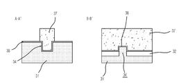
도 5a는 도 4d의 셀트랜지스터영역에 형성된 새들형 트랜지스터의 단면도이고, 도 5b는 도 4d의 주변회로트랜지스터영역에 형성된 핀형 트랜지스터의 단면도이다.FIG. 5A is a cross-sectional view of a saddle transistor formed in the cell transistor region of FIG. 4D, and FIG. 5B is a cross-sectional view of a fin transistor formed in the peripheral circuit transistor region of FIG. 4D.
도 5a의 A-A' 방향의 단면도를 참조하면, 활성영역(31)의 소정 부분에 리세스된 새들형채널(34)이 형성되고, 새들형채널(34) 상에 게이트절연막(38) 및 게이트전극(37)이 형성된다. 그리고, B-B' 방향의 단면도에서는, 게이트절연막(38) 아래의 새들형 채널(34)이 3면으로 이루어짐을 알 수 있다.Referring to the cross-sectional view along the AA ′ direction of FIG. 5A, a saddle-shaped
도 5b의 C-C' 방향의 단면도를 참조하면, 활성영역(31) 상에 게이트절연막(38) 및 게이트전극(37)이 형성된다. 그리고, D-D' 방향의 단면도에서는, 게이트절연막(38) 아래의 핀형 채널(36)이 3면으로 이루어짐을 알 수 있다.Referring to the cross-sectional view of the C-C 'direction of FIG. 5B, the
상술한 본 발명은 셀트랜지스터영역에는 0.8V 이상의 높은 문턱전압을 가지 는 새들형 트랜지스터를 형성하고, 주변회로트랜지스터영역에는 0.1V∼0.4V 정도의 낮은 문턱전압을 가지는 핀형 트랜지스터를 형성하므로써, 셀트랜지스터영역에는 적정 수준의 높은 문턱전압을 유지함과 동시에 셀전류 특성도 양호하게 유지하고, 주변회로트랜지스터영역에서는 핀형 트랜지스터로 인해 전류구동력을 극대화시켜 고속, 저전력을 구현할 수 있다.The present invention described above forms a saddle-type transistor having a high threshold voltage of 0.8 V or more in the cell transistor region, and a pin transistor having a low threshold voltage of about 0.1 V to 0.4 V in the peripheral circuit transistor region, thereby forming a cell transistor. In the region, the threshold voltage is maintained at an appropriate level and the cell current characteristics are maintained well. In the peripheral circuit transistor region, the pin-type transistor maximizes the current driving force to realize high speed and low power.
본 발명의 기술 사상은 상기 바람직한 실시예에 따라 구체적으로 기술되었으나, 상기한 실시예는 그 설명을 위한 것이며 그 제한을 위한 것이 아님을 주의하여야 한다. 또한, 본 발명의 기술 분야의 통상의 전문가라면 본 발명의 기술 사상의 범위 내에서 다양한 실시예가 가능함을 이해할 수 있을 것이다.Although the technical idea of the present invention has been described in detail according to the above preferred embodiment, it should be noted that the above-described embodiment is for the purpose of description and not of limitation. In addition, those skilled in the art will understand that various embodiments are possible within the scope of the technical idea of the present invention.
상술한 본 발명은 셀트랜지스터영역에는 0.8V 이상의 높은 문턱전압을 가지는 새들형 트랜지스터를 형성하고, 주변회로트랜지스터영역에는 0.1V∼0.4V 정도의 낮은 문턱전압을 가지는 핀형 트랜지스터를 형성하므로써, 셀트랜지스터영역에는 적정 수준의 높은 문턱전압을 유지함과 동시에 셀전류 특성도 양호하게 유지할 수 있고, 주변회로트랜지스터영역에서는 핀형 트랜지스터로 인해 전류구동력을 극대화시켜 고속, 저전력을 구현할 수 있는 효과가 있다.The present invention described above forms a saddle-type transistor having a high threshold voltage of 0.8 V or more in the cell transistor region and a pin transistor having a low threshold voltage of about 0.1 V to 0.4 V in the peripheral circuit transistor region, thereby forming a cell transistor region. In addition, it is possible to maintain a high threshold voltage at an appropriate level and to maintain cell current characteristics well, and to realize high speed and low power by maximizing current driving force due to the pin-type transistor in the peripheral circuit transistor region.
Claims (6)
Priority Applications (1)
| Application Number | Priority Date | Filing Date | Title |
|---|---|---|---|
| KR1020060019655A KR100719180B1 (en) | 2006-02-28 | 2006-02-28 | A memory device having a saddle type transistor and a pin type transistor at the same time and a manufacturing method |
Applications Claiming Priority (1)
| Application Number | Priority Date | Filing Date | Title |
|---|---|---|---|
| KR1020060019655A KR100719180B1 (en) | 2006-02-28 | 2006-02-28 | A memory device having a saddle type transistor and a pin type transistor at the same time and a manufacturing method |
Publications (1)
| Publication Number | Publication Date |
|---|---|
| KR100719180B1 true KR100719180B1 (en) | 2007-05-17 |
Family
ID=38277438
Family Applications (1)
| Application Number | Title | Priority Date | Filing Date |
|---|---|---|---|
| KR1020060019655A Expired - Fee Related KR100719180B1 (en) | 2006-02-28 | 2006-02-28 | A memory device having a saddle type transistor and a pin type transistor at the same time and a manufacturing method |
Country Status (1)
| Country | Link |
|---|---|
| KR (1) | KR100719180B1 (en) |
Cited By (1)
| Publication number | Priority date | Publication date | Assignee | Title |
|---|---|---|---|---|
| US8026138B2 (en) | 2008-05-30 | 2011-09-27 | Hynix Semiconductor Inc. | Method for manufacturing semiconductor apparatus having saddle-fin transistor and semiconductor apparatus fabricated thereby |
Citations (4)
| Publication number | Priority date | Publication date | Assignee | Title |
|---|---|---|---|---|
| US6800910B2 (en) * | 2002-09-30 | 2004-10-05 | Advanced Micro Devices, Inc. | FinFET device incorporating strained silicon in the channel region |
| US20050239242A1 (en) * | 2004-04-23 | 2005-10-27 | International Business Machines Corporation | structure and method of manufacturing a finFet device having stacked fins |
| US6970373B2 (en) * | 2003-10-02 | 2005-11-29 | Intel Corporation | Method and apparatus for improving stability of a 6T CMOS SRAM cell |
| US6974983B1 (en) * | 2004-02-02 | 2005-12-13 | Advanced Micro Devices, Inc. | Isolated FinFET P-channel/N-channel transistor pair |
-
2006
- 2006-02-28 KR KR1020060019655A patent/KR100719180B1/en not_active Expired - Fee Related
Patent Citations (4)
| Publication number | Priority date | Publication date | Assignee | Title |
|---|---|---|---|---|
| US6800910B2 (en) * | 2002-09-30 | 2004-10-05 | Advanced Micro Devices, Inc. | FinFET device incorporating strained silicon in the channel region |
| US6970373B2 (en) * | 2003-10-02 | 2005-11-29 | Intel Corporation | Method and apparatus for improving stability of a 6T CMOS SRAM cell |
| US6974983B1 (en) * | 2004-02-02 | 2005-12-13 | Advanced Micro Devices, Inc. | Isolated FinFET P-channel/N-channel transistor pair |
| US20050239242A1 (en) * | 2004-04-23 | 2005-10-27 | International Business Machines Corporation | structure and method of manufacturing a finFet device having stacked fins |
Cited By (1)
| Publication number | Priority date | Publication date | Assignee | Title |
|---|---|---|---|---|
| US8026138B2 (en) | 2008-05-30 | 2011-09-27 | Hynix Semiconductor Inc. | Method for manufacturing semiconductor apparatus having saddle-fin transistor and semiconductor apparatus fabricated thereby |
Similar Documents
| Publication | Publication Date | Title |
|---|---|---|
| KR100720238B1 (en) | Semiconductor element and manufacturing method thereof | |
| KR100748261B1 (en) | FINE field effect transistor with low leakage current and its manufacturing method | |
| US7842594B2 (en) | Semiconductor device and method for fabricating the same | |
| KR100881818B1 (en) | Method of forming a semiconductor device | |
| US7683437B2 (en) | Semiconductor device having fin field effect transistor and manufacturing method thereof | |
| US8269271B2 (en) | Hybrid planarFET and FinFET provided on a chip | |
| JP2006303451A (en) | Semiconductor device and manufacturing method of semiconductor device | |
| KR100608380B1 (en) | Transistor of memory device and method for fabricating the same | |
| CN100590816C (en) | Manufacturing method of recessed gate in semiconductor device | |
| KR100720232B1 (en) | Method of forming a semiconductor device having a fin structure | |
| JP2008523610A (en) | Saddle type MOS element | |
| JP2007201402A (en) | Manufacturing method of semiconductor device | |
| KR101078726B1 (en) | Semiconductor device and method of manufacturing the same | |
| KR100610421B1 (en) | Manufacturing Method of Semiconductor Device | |
| KR20090039203A (en) | Manufacturing Method of Semiconductor Device | |
| KR20040014841A (en) | Manufacturing method for vertical transistor | |
| KR100719180B1 (en) | A memory device having a saddle type transistor and a pin type transistor at the same time and a manufacturing method | |
| KR100806610B1 (en) | Manufacturing method of semiconductor integrated circuit device | |
| KR100854502B1 (en) | Semiconductor device adopting transistor having recess channel region and manufacturing method thereof | |
| KR20060130322A (en) | Field effect transistor having vertical channel and manufacturing method thereof | |
| US7374975B2 (en) | Method of fabricating a transistor | |
| KR100701700B1 (en) | Transistor and manufacturing method | |
| KR100753051B1 (en) | Saddle Pin Transistor Manufacturing Method | |
| KR19990053973A (en) | Structure and Fabrication Method of Highly Integrated Low Voltage YPyrom Cell Based on Self Aligning Recessed Channel Structure | |
| KR100912962B1 (en) | Transistor having multi-channel and manufacturing method of semiconductor device having same |
Legal Events
| Date | Code | Title | Description |
|---|---|---|---|
| A201 | Request for examination | ||
| PA0109 | Patent application |
St.27 status event code: A-0-1-A10-A12-nap-PA0109 |
|
| PA0201 | Request for examination |
St.27 status event code: A-1-2-D10-D11-exm-PA0201 |
|
| D13-X000 | Search requested |
St.27 status event code: A-1-2-D10-D13-srh-X000 |
|
| D14-X000 | Search report completed |
St.27 status event code: A-1-2-D10-D14-srh-X000 |
|
| E902 | Notification of reason for refusal | ||
| PE0902 | Notice of grounds for rejection |
St.27 status event code: A-1-2-D10-D21-exm-PE0902 |
|
| P11-X000 | Amendment of application requested |
St.27 status event code: A-2-2-P10-P11-nap-X000 |
|
| P13-X000 | Application amended |
St.27 status event code: A-2-2-P10-P13-nap-X000 |
|
| E701 | Decision to grant or registration of patent right | ||
| PE0701 | Decision of registration |
St.27 status event code: A-1-2-D10-D22-exm-PE0701 |
|
| GRNT | Written decision to grant | ||
| PR0701 | Registration of establishment |
St.27 status event code: A-2-4-F10-F11-exm-PR0701 |
|
| PR1002 | Payment of registration fee |
St.27 status event code: A-2-2-U10-U11-oth-PR1002 Fee payment year number: 1 |
|
| PG1601 | Publication of registration |
St.27 status event code: A-4-4-Q10-Q13-nap-PG1601 |
|
| PR1001 | Payment of annual fee |
St.27 status event code: A-4-4-U10-U11-oth-PR1001 Fee payment year number: 4 |
|
| FPAY | Annual fee payment |
Payment date: 20110429 Year of fee payment: 5 |
|
| PR1001 | Payment of annual fee |
St.27 status event code: A-4-4-U10-U11-oth-PR1001 Fee payment year number: 5 |
|
| PN2301 | Change of applicant |
St.27 status event code: A-5-5-R10-R13-asn-PN2301 St.27 status event code: A-5-5-R10-R11-asn-PN2301 |
|
| LAPS | Lapse due to unpaid annual fee | ||
| PC1903 | Unpaid annual fee |
St.27 status event code: A-4-4-U10-U13-oth-PC1903 Not in force date: 20120511 Payment event data comment text: Termination Category : DEFAULT_OF_REGISTRATION_FEE |
|
| PN2301 | Change of applicant |
St.27 status event code: A-5-5-R10-R13-asn-PN2301 St.27 status event code: A-5-5-R10-R11-asn-PN2301 |
|
| PC1903 | Unpaid annual fee |
St.27 status event code: N-4-6-H10-H13-oth-PC1903 Ip right cessation event data comment text: Termination Category : DEFAULT_OF_REGISTRATION_FEE Not in force date: 20120511 |
|
| PN2301 | Change of applicant |
St.27 status event code: A-5-5-R10-R13-asn-PN2301 St.27 status event code: A-5-5-R10-R11-asn-PN2301 |
|
| P22-X000 | Classification modified |
St.27 status event code: A-4-4-P10-P22-nap-X000 |
|
| P22-X000 | Classification modified |
St.27 status event code: A-4-4-P10-P22-nap-X000 |
|
| P22-X000 | Classification modified |
St.27 status event code: A-4-4-P10-P22-nap-X000 |