KR100713408B1 - Single Sideband Modulation Module and Single Sideband Modulation Means - Google Patents
Single Sideband Modulation Module and Single Sideband Modulation Means Download PDFInfo
- Publication number
- KR100713408B1 KR100713408B1 KR1020050081282A KR20050081282A KR100713408B1 KR 100713408 B1 KR100713408 B1 KR 100713408B1 KR 1020050081282 A KR1020050081282 A KR 1020050081282A KR 20050081282 A KR20050081282 A KR 20050081282A KR 100713408 B1 KR100713408 B1 KR 100713408B1
- Authority
- KR
- South Korea
- Prior art keywords
- single sideband
- carrier frequency
- mach
- arm
- sideband modulation
- Prior art date
- Legal status (The legal status is an assumption and is not a legal conclusion. Google has not performed a legal analysis and makes no representation as to the accuracy of the status listed.)
- Expired - Fee Related
Links
Images


Classifications
-
- H—ELECTRICITY
- H04—ELECTRIC COMMUNICATION TECHNIQUE
- H04B—TRANSMISSION
- H04B1/00—Details of transmission systems, not covered by a single one of groups H04B3/00 - H04B13/00; Details of transmission systems not characterised by the medium used for transmission
- H04B1/68—Details of transmission systems, not covered by a single one of groups H04B3/00 - H04B13/00; Details of transmission systems not characterised by the medium used for transmission for wholly or partially suppressing the carrier or one side band
-
- G—PHYSICS
- G02—OPTICS
- G02B—OPTICAL ELEMENTS, SYSTEMS OR APPARATUS
- G02B6/00—Light guides; Structural details of arrangements comprising light guides and other optical elements, e.g. couplings
- G02B6/24—Coupling light guides
- G02B6/26—Optical coupling means
- G02B6/264—Optical coupling means with optical elements between opposed fibre ends which perform a function other than beam splitting
- G02B6/266—Optical coupling means with optical elements between opposed fibre ends which perform a function other than beam splitting the optical element being an attenuator
-
- H—ELECTRICITY
- H04—ELECTRIC COMMUNICATION TECHNIQUE
- H04L—TRANSMISSION OF DIGITAL INFORMATION, e.g. TELEGRAPHIC COMMUNICATION
- H04L27/00—Modulated-carrier systems
- H04L27/02—Amplitude-modulated carrier systems, e.g. using on-off keying; Single sideband or vestigial sideband modulation
- H04L27/04—Modulator circuits; Transmitter circuits
-
- G—PHYSICS
- G02—OPTICS
- G02F—OPTICAL DEVICES OR ARRANGEMENTS FOR THE CONTROL OF LIGHT BY MODIFICATION OF THE OPTICAL PROPERTIES OF THE MEDIA OF THE ELEMENTS INVOLVED THEREIN; NON-LINEAR OPTICS; FREQUENCY-CHANGING OF LIGHT; OPTICAL LOGIC ELEMENTS; OPTICAL ANALOGUE/DIGITAL CONVERTERS
- G02F2203/00—Function characteristic
- G02F2203/48—Variable attenuator
Landscapes
- Engineering & Computer Science (AREA)
- Computer Networks & Wireless Communication (AREA)
- Signal Processing (AREA)
- Physics & Mathematics (AREA)
- General Physics & Mathematics (AREA)
- Optics & Photonics (AREA)
- Optical Modulation, Optical Deflection, Nonlinear Optics, Optical Demodulation, Optical Logic Elements (AREA)
- Optical Communication System (AREA)
Abstract
본 발명에 따른 반송 주파수를 이용한 단측파대 변조 모듈은 상기 반송 주파수와 제1 및 제2 신호를 단측파대 신호로 변조시키기 위한 제1 및 제2 마하젠더 간섭계와, 상기 제1 및 제2 마하젠더 간섭계들이 결합된 양 끝단들과 연결되며 상기 반송 주파수를 분할해서 분할된 일부를 상기 제1 및 제2 마하젠더 간섭계로 출력하기 위한 암을 포함한다.A single sideband modulation module using a carrier frequency according to the present invention includes first and second Mach-Zehnder interferometers for modulating the carrier frequency and first and second signals into single-sideband signals, and the first and second Mach-Zehnder interferometers. And an arm for splitting the carrier frequency and outputting the divided part to the first and second Mach-Zehnder interferometers.
마하젠더, 단측파대, 변조기 Mach-Zehnder, Single Sideband, Modulator
Description
도 1은 종래의 단측파대 변조 수단의 구성을 나타내는 도면,1 is a diagram showing the configuration of a conventional single sideband modulation means;
도 2는 반송 주파수의 세기에 따른 아이 다이그램을 도시한 그래프,2 is a graph showing an eye diagram according to the strength of a carrier frequency;
도 3은 본 발명의 제1 실시 예에 따른 단측파대 변조 수단의 구성을 나타내는 도면,3 is a diagram showing the configuration of a single sideband modulation means according to a first embodiment of the present invention;
도 4는 본 발명의 제2 실시 예에 따른 단측파대 변조 수단의 구성을 나타내는 도면,4 is a diagram showing the configuration of a single sideband modulation means according to a second embodiment of the present invention;
도 5는 본 발명의 제3 실시 예에 따른 단측파대 변조 수단의 구성을 나타내는 도면, 5 is a diagram showing the configuration of a single sideband modulation means according to a third embodiment of the present invention;
도 6은 본 발명의 제4 실시 예에 따른 단측파대 변조 수단의 구성을 나타내는 도면.6 is a diagram showing the configuration of a single sideband modulation means according to a fourth embodiment of the present invention;
본 발명은 단측파대 전송(single side band transmission)을 위한 단측파대 변조 수단에 관한 발명으로서, 특히 반송 주파수를 동시에 전송할 수 있는 단측파대 변조 수단에 관한 발명이다. The present invention relates to a single sideband modulation means for single side band transmission, and more particularly to a single sideband modulation means capable of transmitting carrier frequencies at the same time.
진폭 변조된 데이터를 반송 주파수로 변조시킨 피변조된 신호의 스펙트럼은 반송 주파수를 대칭축으로 2개의 상측 및 하측 파대(Upper Side Band & Lower side band)를 형성한다. 또한, 피변조된 신호의 전송 방식 중 반송 주파수 및 일 측파대(Side band)를 제거하고 단일 측 파대만 이용한 신호의 전송 방식을 단측파대 전송(Single Side Band) 전송 방식이라고 한다. The spectrum of the modulated signal that modulates the amplitude modulated data at the carrier frequency forms two upper and lower side bands at the axis of symmetry of the carrier frequency. In addition, the transmission method of a signal using only a single sideband by removing a carrier frequency and side bands among the transmission methods of a modulated signal is called a single side band transmission method.
상술한 상측 파대는 피변조된 신호의 채널들을 높은 주파수대로 이동시킨 것을 의미하고, 하측 파대는 피변조된 신호의 채널들을 반전시켜서 낮은 주파수대로 이동시킨 파대를 의미한다. The above-described upper band means that the channels of the modulated signal are shifted to a higher frequency, and the lower band means the shifting of the channels of the modulated signal to a lower frequency.
단측파대 전송은 양측파대 전송에 비해서 점유 주파수 폭이 1/2이고, 반송 파 및 일 측파대를 전송하지 않음으로 증폭기 등의 소요 전력을 최소화시킬 수 있다. 또한, 대역 폭이 좁음으로 잡음이 감소되어 신호대 잡음비 및 수신감도가 개선된다. 상술한 단측파대 전송을 위한 단측파대 변조 수단은 광섬유 브래그 격자를 사용해서 광 도메인에서 필터링 해주는 방법이 사용되고 있으며, 상술한 경우 광섬유 브래그 격자 제작이 용이하지 않을 뿐 아니라 안정성(stability)이 저하되어 실제 사용이 어렵다. 상술한 SSB 변조 수단의 문제를 해결하기 위한 안정성이 우수한 LiNbO3 기반의 단측파대 변조 수단이 제안되고 있다. Single-sideband transmission has a half occupied frequency width compared to bilateral transmission, and does not transmit a carrier wave and one sideband, thereby minimizing power consumption of an amplifier. In addition, the narrow bandwidth reduces noise to improve signal-to-noise ratio and reception sensitivity. As the above-described single sideband modulation means for transmitting the single sideband, a method of filtering in the optical domain using an optical fiber Bragg grating has been used. This is difficult. LiNbO 3 based single sideband modulation means having excellent stability for solving the problems of the SSB modulation means described above has been proposed.
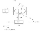
도 1은 단측파대 전송을 위한 종래 단측파대 변조 수단의 구성을 나타낸다. 도 1을 참조하면 단측파대 변조 수단(100)은 단측파대 변조 모듈(110)과, 하이브리드 결합기(Hybrid coupler; 130)와, 광원(120)을 포함한다. 상기 광원(120)은 반송 주파수를 생성한다. 상기 하이브리드 결합기(130)는 입력되는 데이터 (a)를 0°와 90°도 위상을 갖는 제1 및 제2 신호들을 형성해서 상기 단측파대 변조 모듈(110)로 출력한다. 1 shows a configuration of a conventional single sideband modulation means for single sideband transmission. Referring to FIG. 1, the single sideband modulation means 100 includes a single
상기 SSB 변조 모듈(110)은 다수의 암들을 구비한 LiNbO3 기반의 마하 젠더 간섭계들(111, 112)로 구성되며, 상기 하이브리드 결합기(130)로부터 입력된 각각 0°와 90°도 위상의 제1 및 제2 신호들을 (b)와 같은 단측파대 신호로 결합시켜서 출력한다. The
반송 주파수의 세기에 따른 아이다이어 그램의 변화를 나타내는 도 2의 a 내지 d를 참조하면 반송 주파수가 가장 작은 경우의 도 2의 a에 도시된 아이 다이어그램이 가장 작고, 반송 주파수 주파수가 가장 큰 도 2의 d에 도시된 아이 다이어그램이 가장 크고 선명하게 나타남을 알 수 있다. Referring to a to d of FIG. 2 showing a change in the eye diagram according to the strength of the carrier frequency, the eye diagram shown in a of FIG. 2 when the carrier frequency is the smallest and the carrier frequency frequency is the largest in FIG. It can be seen that the eye diagram shown at d is the largest and clearest.
또한, 반송 주파수 주파수가 제거된 SSB 변조는 직접 검출 방식의 수신기를 사용할 수 없고, 복잡한 형태의 광 간섭계 형태의 검출기를 사용해야되는 문제가 있다. In addition, SSB modulation in which the carrier frequency frequency is removed cannot be used with a direct detection receiver, and there is a problem in that a detector of a complex optical interferometer type is used.
상술한 문제를 해결하기 위해서 기존 SSB 변조 수단에 약간의 옵셋을 인가하는 방법도 있으나, 이 경우에 원하지 않는 타 측 파대가 혼합되는 문제가 있다. 즉, 상측파대 신호 전송 시 하측파대 신호가 혼합되거나, 하측파대 신호 전송 시 상 측파대 신호가 혼합되는 문제를 유발할 수 있다.In order to solve the above-mentioned problem, there is also a method of applying a slight offset to the existing SSB modulation means, but in this case, there is a problem in that the other unwanted band is mixed. That is, the lower sideband signal may be mixed when the upper sideband signal is transmitted, or the upper sideband signal may be mixed when the lower sideband signal is transmitted.
본 발명의 목적은 상술한 문제점들을 해결하기 위해서 반송 주파수을 포함하는 단측파대 신호의 전송이 가능한 단측파대 변조 모듈을 제공하는 데 있다. SUMMARY OF THE INVENTION An object of the present invention is to provide a single sideband modulation module capable of transmitting a single sideband signal including a carrier frequency in order to solve the above problems.
본 발명에 따른 반송 주파수를 이용한 단측파대 변조 모듈은,Single sideband modulation module using a carrier frequency according to the present invention,
상기 반송 주파수와 제1 및 제2 신호를 단측파대 신호로 변조시키기 위한 제1 및 제2 마하젠더 간섭계와;First and second Mach-Zehnder interferometers for modulating the carrier frequency and the first and second signals into a single sideband signal;
상기 제1 및 제2 마하젠더 간섭계들이 결합된 양 끝단들과 연결되며 상기 반송 주파수를 분할해서 분할된 일부를 상기 제1 및 제2 마하젠더 간섭계로 출력하기 위한 암을 포함한다.And an arm connected to both ends of the first and second Mach-Zehnder interferometers, and configured to divide the carrier frequency and output the divided portion to the first and second Mach-Zehnder interferometers.
이하에서는 첨부도면들을 참조하여 본 발명의 실시 예를 상세히 설명하기로 한다. 본 발명을 설명함에 있어서, 관련된 공지기능, 혹은 구성에 대한 구체적인 설명은 본 발명의 요지를 모호하지 않게 하기 위하여 생략한다.Hereinafter, with reference to the accompanying drawings will be described an embodiment of the present invention; In describing the present invention, detailed descriptions of related well-known functions or configurations are omitted in order not to obscure the subject matter of the present invention.
도 3은 본 발명의 제1 실시 예에 따른 단측파대 변조 수단의 구성을 나타내는 도면이다. 본 실시 예에 따른 단측파대 변조 수단(200)은 반송 주파수(a)를 생성하기 위한 광원(220)과, 외부로부터 입력된 데이터(b)를 90도의 위상차를 갖는 제1 및 제2 신호를 생성하는 하이브리드 결합기(230)과, 단측파대 변조 모듈(210) 을 포함한다. 상기 광원(220)는 CW 방식의 레이저를 포함할 수 있다.3 is a diagram showing the configuration of a single sideband modulation means according to the first embodiment of the present invention. The single-side band modulating means 200 according to the present embodiment generates a
상기 단측파대 변조 모듈(210)은 상기 반송 주파수와 제1 및 제2 신호를 단측파대 신호(c)로 변조시키기 위한 제1 및 제2 마하젠더 간섭계(211, 212)와, 암(213)을 포함한다. The single
상기 암(213)은 상기 제1 및 제2 마하젠더 간섭계들(211, 212)이 결합된 양 끝단에 연결된 이분기 도파로(Y-branch) 구조로서, 상기 광원(220)으로부터 입력된 상기 반송 주파수를 세기 분할해서 일부를 상기 제1 및 제2 마하젠더 간섭계(211, 212)로 출력하고 또 다른 반송 주파수(a)의 일부를 상기 제1 및 제2 마하젠더 간섭계(211, 212)에서 변조된 단측파대 신호(c)에 결합해서 반송 주파수(a)를 포함하는 단측파대 신호(d)를 상기 단측파대 변조 모듈(210)의 외부로 출력한다. 또한, 상기 암(213)에서 분할되는 상기 반송 주파수의 비율을 필요에 의해 조절할 수 있으며, 분할되는 비율에 따라서 최종적으로 출력되는 단측파대 신호에 포함된 반송 주파수의 크기가 결정될 수 있다. The
도 4는 본 발명의 제2 실시 예에 따른 단측파대 변조 수단의 구성을 나타내는 도면이다. 도 4를 참조하면, 본 실시 예에 따른 단측파대 변조 수단(300)은 반송 주파수(a)를 생성하기 위한 광원(320)과, 외부로부터 입력된 데이터(b)를 90도의 위상차를 갖는 제1 및 제2 신호로 생성하는 하이브리드 결합기(330)와, 단측파대 변조 모듈(310)을 포함한다.4 is a diagram showing the configuration of a single sideband modulation means according to a second embodiment of the present invention. Referring to FIG. 4, the single sideband modulating means 300 according to the present embodiment includes a
상기 단측파대 변조 모듈(310)은 상기 반송 주파수와 제1 및 제2 신호를 단측파대 신호(c)로 변조시키기 위한 제1 및 제2 마하젠더 간섭계(311, 312)와, 상기 단측파대 신호(c)에 상기 광원(320)에서 생성된 반송 주파수를 결합시키기 위한 암(313)을 포함한다. The single
상기 암(313)은 상기 제1 및 제2 마하젠더 간섭계들(311, 312)의 양 끝단을 연결하며, 그 사이를 가로지르게 위치된다. The
도 5는 본 발명의 제3 실시 예에 따른 단측파대 변조 수단의 구성을 나타내는 도면이다. 도 5를 참조하면, 본 실시 예에 따른 단측파대 변조 수단(400)은 반송 주파수를 생성하기 위한 광원(420)과, 데이터로부터 90도의 위상차를 갖는 제1 및 제2 신호를 생성하기 위한 하이브리드 결합기(430)과, 단측파대 변조 모듈(410)을 포함한다.5 is a diagram showing the configuration of a single sideband modulation means according to a third embodiment of the present invention. Referring to FIG. 5, the single sideband modulating means 400 according to the present embodiment includes a
상기 단측파대 변조 모듈(410)은 상기 반송 주파수와 제1 및 제2 신호를 단측파대 신호로 변조시키기 위한 제1 및 제2 마하젠더 간섭계(411, 412)와, 암(413)과, 상기 암(413) 상에 위치된 가변 광 감쇄기(414)를 포함한다. The single
상기 암(413)은 상기 제1 및 제2 마하젠더 간섭계들(411, 412)이 결합된 양 끝단에 연결된 이분기 도파로(Y-branch) 구조로서, 상기 광원(420)으로부터 입력된 상기 반송 주파수를 세기 분할한다. 상기 가변 광 감쇄기(414)는 상기 반송 주파수의 세기를 조절할 수 있다. The
도 6은 본 발명의 제4 실시 예에 따른 단측파대 변조 수단의 구성을 나타내는 도면이다. 도 6을 참조하면, 본 실시 예에 따른 단측파대 변조 수단(500)은 반송 주파수를 생성하기 위한 광원(520)과, 외부로부터 입력된 데이터로부터 90도의 위상차를 갖는 제1 및 제2 신호를 생성하기 위한 하이브리드 결합기(530)와, 단측 파대 변조 모듈(510)을 포함한다.6 is a diagram showing the configuration of a single sideband modulation means according to a fourth embodiment of the present invention. Referring to FIG. 6, the single sideband modulating means 500 according to the present embodiment generates a
상기 단측파대 변조 모듈(510)은 단측파대 신호를 생성하기 위한 제1 및 제2 마하젠더 간섭계(511, 512)와, 상기 단측파대 신호에 반송 주파수를 결합시키기 위한 암(513)과, 상기 암(513) 상에 위치된 가변 광 감쇄기(514)를 포함한다. The single
본 발명에 따른 단측파대 변조 모듈은 반소 주파스를 분할하기 위한 암을 더 포함하으로써 반송 주파수을 포함하는 단측파대 신호를 생성할 수 있다. 따라서, 본 발명은 기존에 반송 주파수을 포함하는 단측파대 신호를 생성하기 위한 변조기들의 경우 발생 가능한 원하지 않는 단측파대의 발생을 억제할 수 있고, 필요에 따라서는 반송 주파수의 세기도 제어할 수 있는 이점이 있다. The single sideband modulation module according to the present invention may further include an arm for dividing the half-segment frequency, thereby generating a single sideband signal including a carrier frequency. Accordingly, the present invention can suppress the generation of unwanted single sidebands that can occur in the case of modulators for generating a single sideband signal including the carrier frequency, and control the strength of the carrier frequency as necessary. have.
Claims (8)
Priority Applications (2)
| Application Number | Priority Date | Filing Date | Title |
|---|---|---|---|
| KR1020050081282A KR100713408B1 (en) | 2005-09-01 | 2005-09-01 | Single Sideband Modulation Module and Single Sideband Modulation Means |
| US11/514,438 US20070047668A1 (en) | 2005-09-01 | 2006-09-01 | Single side band modulator module and single side band modulator device using the same |
Applications Claiming Priority (1)
| Application Number | Priority Date | Filing Date | Title |
|---|---|---|---|
| KR1020050081282A KR100713408B1 (en) | 2005-09-01 | 2005-09-01 | Single Sideband Modulation Module and Single Sideband Modulation Means |
Publications (2)
| Publication Number | Publication Date |
|---|---|
| KR20070025285A KR20070025285A (en) | 2007-03-08 |
| KR100713408B1 true KR100713408B1 (en) | 2007-05-04 |
Family
ID=37804069
Family Applications (1)
| Application Number | Title | Priority Date | Filing Date |
|---|---|---|---|
| KR1020050081282A Expired - Fee Related KR100713408B1 (en) | 2005-09-01 | 2005-09-01 | Single Sideband Modulation Module and Single Sideband Modulation Means |
Country Status (2)
| Country | Link |
|---|---|
| US (1) | US20070047668A1 (en) |
| KR (1) | KR100713408B1 (en) |
Families Citing this family (4)
| Publication number | Priority date | Publication date | Assignee | Title |
|---|---|---|---|---|
| JP2005100100A (en) * | 2003-09-25 | 2005-04-14 | Toyota Motor Corp | Wheel information processing apparatus and wheel information processing method |
| GB0904600D0 (en) | 2009-03-18 | 2009-04-29 | Cip Technologies Ltd | Optical single-sideband transmitter |
| US20150256265A1 (en) * | 2014-03-07 | 2015-09-10 | Futurewei Technologies, Inc. | System and Method for Chromatic Dispersion Tolerant Direct Optical Detection |
| KR102470157B1 (en) * | 2018-12-13 | 2022-11-24 | 한국전자통신연구원 | Apparatus and method for generating single sideband based on laser diode |
Citations (4)
| Publication number | Priority date | Publication date | Assignee | Title |
|---|---|---|---|---|
| KR970705042A (en) * | 1995-06-05 | 1997-09-06 | 미야지 모사노리 | Electromagnetic Actuator |
| KR20000022321A (en) * | 1996-06-28 | 2000-04-25 | 더 거번먼트 오브 더 유나이티드 스테이츠 오브 아메리카, 애즈 레프리젠티드 바이 더 세크러테리 오브 더 네이비 네이벌 리서치 래보러토리 | Optical sensor system utilizing bragg grating sensors |
| KR20030070225A (en) * | 2002-02-21 | 2003-08-29 | 한국전자통신연구원 | Methods for compensating the polarization mode dispersion occurring in an optical transmission fiber and an apparatus therefor |
| KR20040025206A (en) * | 2002-09-18 | 2004-03-24 | 엘지전자 주식회사 | Electrostatic dual axis micro mirror and manufacturing method thereof |
Family Cites Families (1)
| Publication number | Priority date | Publication date | Assignee | Title |
|---|---|---|---|---|
| JP4646048B2 (en) * | 2001-03-02 | 2011-03-09 | 日本電気株式会社 | Single sideband signal light generation method and single sideband signal light generation circuit |
-
2005
- 2005-09-01 KR KR1020050081282A patent/KR100713408B1/en not_active Expired - Fee Related
-
2006
- 2006-09-01 US US11/514,438 patent/US20070047668A1/en not_active Abandoned
Patent Citations (4)
| Publication number | Priority date | Publication date | Assignee | Title |
|---|---|---|---|---|
| KR970705042A (en) * | 1995-06-05 | 1997-09-06 | 미야지 모사노리 | Electromagnetic Actuator |
| KR20000022321A (en) * | 1996-06-28 | 2000-04-25 | 더 거번먼트 오브 더 유나이티드 스테이츠 오브 아메리카, 애즈 레프리젠티드 바이 더 세크러테리 오브 더 네이비 네이벌 리서치 래보러토리 | Optical sensor system utilizing bragg grating sensors |
| KR20030070225A (en) * | 2002-02-21 | 2003-08-29 | 한국전자통신연구원 | Methods for compensating the polarization mode dispersion occurring in an optical transmission fiber and an apparatus therefor |
| KR20040025206A (en) * | 2002-09-18 | 2004-03-24 | 엘지전자 주식회사 | Electrostatic dual axis micro mirror and manufacturing method thereof |
Non-Patent Citations (4)
| Title |
|---|
| 한국공개특허공보제00-22321 |
| 한국공개특허공보제03-70225 |
| 한국공개특허공보제04-25206 |
| 한국공개특허공보제97-705042 |
Also Published As
| Publication number | Publication date |
|---|---|
| US20070047668A1 (en) | 2007-03-01 |
| KR20070025285A (en) | 2007-03-08 |
Similar Documents
| Publication | Publication Date | Title |
|---|---|---|
| EP2148457A2 (en) | Optical transmitter | |
| JP4646048B2 (en) | Single sideband signal light generation method and single sideband signal light generation circuit | |
| US6643046B2 (en) | Apparatus and method for optical modulation | |
| KR101958867B1 (en) | Carrier-suppressed light-generating device | |
| US9337936B2 (en) | Optical transmission apparatus, optical transmission method and program for optical transmission | |
| JP4878358B2 (en) | Optical SSB modulator | |
| KR20060084259A (en) | Offset Quadrature Phase Shift Keying Method and Optical Transmitter | |
| US20140043673A1 (en) | Method and device for converting optical frequency | |
| JP3432957B2 (en) | Optical modulator and optical fiber communication system | |
| EP3291462A1 (en) | Dummy light generation device, light transmission device, and dummy light generation method | |
| KR100713408B1 (en) | Single Sideband Modulation Module and Single Sideband Modulation Means | |
| KR100640509B1 (en) | Single Sideband Modulation Module | |
| JP4494347B2 (en) | Light modulator | |
| US20190020418A1 (en) | Optical transmitter, optical transmission apparatus, and optical modulation method | |
| JP3955292B2 (en) | FM modulator | |
| JP7693399B2 (en) | Optical angle modulator and optical transmitter | |
| KR102494502B1 (en) | Electro-optic modulators and methods for modulating optical beams to carry RF signals | |
| JP4728275B2 (en) | Optical SSB transmitter | |
| WO2002052754A2 (en) | Method, system and apparatus for optically transferring information | |
| JP2000122015A (en) | Light modulator | |
| JP4028463B2 (en) | Optical transmitter and optical transmitter / receiver | |
| JP2004096653A (en) | Optical transmitter and optical modulation method to be used therefor | |
| KR100559138B1 (en) | Optical communication system and its modulation and transmission method | |
| US20080159754A1 (en) | Modulation Light Signal Generating Device and Fsk Modulation Signal Generating Device | |
| JP2021061509A (en) | Polarization multiplexed light transmission device |
Legal Events
| Date | Code | Title | Description |
|---|---|---|---|
| A201 | Request for examination | ||
| PA0109 | Patent application |
St.27 status event code: A-0-1-A10-A12-nap-PA0109 |
|
| PA0201 | Request for examination |
St.27 status event code: A-1-2-D10-D11-exm-PA0201 |
|
| E902 | Notification of reason for refusal | ||
| PE0902 | Notice of grounds for rejection |
St.27 status event code: A-1-2-D10-D21-exm-PE0902 |
|
| P11-X000 | Amendment of application requested |
St.27 status event code: A-2-2-P10-P11-nap-X000 |
|
| P13-X000 | Application amended |
St.27 status event code: A-2-2-P10-P13-nap-X000 |
|
| E701 | Decision to grant or registration of patent right | ||
| PE0701 | Decision of registration |
St.27 status event code: A-1-2-D10-D22-exm-PE0701 |
|
| PG1501 | Laying open of application |
St.27 status event code: A-1-1-Q10-Q12-nap-PG1501 |
|
| GRNT | Written decision to grant | ||
| PR0701 | Registration of establishment |
St.27 status event code: A-2-4-F10-F11-exm-PR0701 |
|
| PR1002 | Payment of registration fee |
St.27 status event code: A-2-2-U10-U11-oth-PR1002 Fee payment year number: 1 |
|
| PG1601 | Publication of registration |
St.27 status event code: A-4-4-Q10-Q13-nap-PG1601 |
|
| PR1001 | Payment of annual fee |
St.27 status event code: A-4-4-U10-U11-oth-PR1001 Fee payment year number: 4 |
|
| PR1001 | Payment of annual fee |
St.27 status event code: A-4-4-U10-U11-oth-PR1001 Fee payment year number: 5 |
|
| FPAY | Annual fee payment | ||
| PR1001 | Payment of annual fee |
St.27 status event code: A-4-4-U10-U11-oth-PR1001 Fee payment year number: 6 |
|
| R18-X000 | Changes to party contact information recorded |
St.27 status event code: A-5-5-R10-R18-oth-X000 |
|
| FPAY | Annual fee payment | ||
| PR1001 | Payment of annual fee |
St.27 status event code: A-4-4-U10-U11-oth-PR1001 Fee payment year number: 7 |
|
| PR1001 | Payment of annual fee |
St.27 status event code: A-4-4-U10-U11-oth-PR1001 Fee payment year number: 8 |
|
| PR1001 | Payment of annual fee |
St.27 status event code: A-4-4-U10-U11-oth-PR1001 Fee payment year number: 9 |
|
| LAPS | Lapse due to unpaid annual fee | ||
| PC1903 | Unpaid annual fee |
St.27 status event code: A-4-4-U10-U13-oth-PC1903 Not in force date: 20160425 Payment event data comment text: Termination Category : DEFAULT_OF_REGISTRATION_FEE |
|
| P22-X000 | Classification modified |
St.27 status event code: A-4-4-P10-P22-nap-X000 |
|
| PC1903 | Unpaid annual fee |
St.27 status event code: N-4-6-H10-H13-oth-PC1903 Ip right cessation event data comment text: Termination Category : DEFAULT_OF_REGISTRATION_FEE Not in force date: 20160425 |
|
| P22-X000 | Classification modified |
St.27 status event code: A-4-4-P10-P22-nap-X000 |