KR100713121B1 - Chips and Chip Stacks Using the Same - Google Patents
Chips and Chip Stacks Using the Same Download PDFInfo
- Publication number
- KR100713121B1 KR100713121B1 KR1020050089724A KR20050089724A KR100713121B1 KR 100713121 B1 KR100713121 B1 KR 100713121B1 KR 1020050089724 A KR1020050089724 A KR 1020050089724A KR 20050089724 A KR20050089724 A KR 20050089724A KR 100713121 B1 KR100713121 B1 KR 100713121B1
- Authority
- KR
- South Korea
- Prior art keywords
- wafer
- metal layer
- chip
- pad
- via hole
- Prior art date
- Legal status (The legal status is an assumption and is not a legal conclusion. Google has not performed a legal analysis and makes no representation as to the accuracy of the status listed.)
- Expired - Fee Related
Links
Images


Classifications
-
- H10W20/023—
-
- H10W20/0234—
-
- H10W20/0242—
-
- H10W20/0249—
-
- H10W20/20—
-
- H10W72/012—
-
- H10W90/00—
-
- H10W72/07251—
-
- H10W72/20—
-
- H10W72/221—
-
- H10W72/244—
-
- H10W72/90—
-
- H10W72/9415—
-
- H10W72/942—
-
- H10W90/297—
-
- H10W90/722—
Landscapes
- Internal Circuitry In Semiconductor Integrated Circuit Devices (AREA)
Abstract
본 발명은 칩과 이를 이용한 칩 스택 및 그 제조방법에 관한 것으로, 웨이퍼상에 형성된 적어도 하나 이상의 패드와 상기 패드의 저면이 노출되도록 상기 웨이퍼를 관통하는 비아홀에 상기 웨이퍼의 저면으로부터 일정한 두께까지 돌출되도록 형성된 금속층을 포함하는 복수개의 칩이 적층되되, 상기 각 칩의 패드와 금속층이 서로 마주보도록 접합되어 적층함으로써, 칩의 제조공정이 간편해지고 칩의 성능을 향상시켜줄 뿐만 아니라 칩 스택 시 풋 프린트(foot print)가 작아지는 효과가 있다.The present invention relates to a chip, a chip stack using the same, and a method of manufacturing the same, wherein the at least one pad formed on the wafer and the via hole penetrating the wafer are exposed to a predetermined thickness from the bottom of the wafer to expose the bottom of the pad. A plurality of chips including the formed metal layers are stacked, and the pads and the metal layers of the chips are bonded to each other so as to face each other, thereby simplifying the chip manufacturing process and improving chip performance, as well as footprint during chip stacking. print) becomes smaller.
칩 스택, 웨이퍼, 패드, 비아홀, 플립칩, 범프, 풋 프린트 Chip Stack, Wafer, Pad, Via Hole, Flip Chip, Bump, Footprint
Description
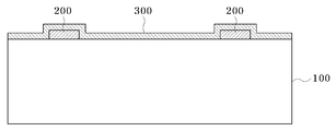
도 1은 본 발명의 일 실시예에 따른 칩을 설명하기 위한 단면도.1 is a cross-sectional view illustrating a chip according to an embodiment of the present invention.
도 2는 본 발명의 일 실시예에 따른 칩 스택을 설명하기 위한 단면도.2 is a cross-sectional view illustrating a chip stack according to an embodiment of the present invention.
도 3a 내지 3g는 본 발명의 일 실시예에 따른 칩의 제조방법을 설명하기 위한 단면도.3A to 3G are cross-sectional views illustrating a method of manufacturing a chip in accordance with one embodiment of the present invention.
*** 도면의 주요 부분에 대한 부호 설명 ****** Explanation of symbols on main parts of drawing ***
100 : 웨이퍼, 200 : 패드,100: wafer, 200: pad,
300 : 시드금속층, 400 : 산화막,300: seed metal layer, 400: oxide film,
400' : 비아홀 형성용 패턴, 500 : 감광막 패턴,400 ': pattern for forming via holes, 500: photoresist pattern,
600 : 비아홀, 700 : 금속층600: via hole, 700: metal layer
본 발명은 칩과 이를 이용한 칩 스택 및 그 제조방법에 관한 것으로, 보다 상세하게는 웨이퍼상에 형성된 패드의 저면이 노출되도록 웨이퍼를 관통하는 비아홀에 웨이퍼의 저면으로부터 일정한 두께까지 돌출되도록 금속층을 형성함으로써, 칩의 제조공정이 간편해지고 칩의 성능을 향상시켜줄 뿐만 아니라 칩 스택 시 풋 프린트(foot print)가 작아질 수 있도록 한 칩과 이를 이용한 칩 스택 및 그 제조방법에 관한 것이다.The present invention relates to a chip, a chip stack using the same, and a method of manufacturing the same, and more particularly, by forming a metal layer protruding from a bottom of a wafer to a predetermined thickness in a via hole penetrating the wafer to expose a bottom of a pad formed on the wafer. In addition, the present invention relates to a chip, a chip stack using the same, and a method of manufacturing the same, which can simplify the manufacturing process of the chip, improve the performance of the chip, and reduce the foot print during the chip stack.
최근에 무선 통신 및 디지털 멀티미디어 수요 증가 및 기술의 발전으로 휴대 단말기, PDA, 고성능 멀티미디어 기기 등 디지털 휴대 전자기기는 소형화, 고성능화, 고집적화 및 다기능화 등을 요구하고 있다.Recently, as the demand for wireless communication and digital multimedia increases and the development of technology, digital portable electronic devices such as portable terminals, PDAs, and high-performance multimedia devices require miniaturization, high performance, high integration, and multifunction.
이와 같이 디지털 휴대 전자기기의 소형화를 위하여 핵심 부품인 반도체 소자를 하나의 칩(chip)에서 시스템 수준의 복합 기능이 가능하도록 서로 다른 기능을 가진 집적회로(Integrated Circuit, IC)들을 원 칩(one chip)화 하는 시스템 온 칩(System on Chip, SoC) 기술 개발에 많은 연구를 하고 있다.In order to miniaturize digital portable electronic devices, integrated circuits (ICs) having different functions are used as one chip to enable a system-level complex function of a semiconductor device, which is a core component, in one chip. He is doing a lot of research on developing System on Chip (SoC) technology.
그러나, 이러한 시스템 온 칩(Soc)은 같은 공정 기술인 집적회로(IC)만을 원 칩(one chip)화 할 수 있다. 즉, 모스(MOS), 바이폴라(Bipolar) 및 RF 칩들은 제조 공정이 서로 다른 기술 즉, 사용하는 웨이퍼 및 공정이 다르므로, 시스템 온 칩(SoC)으로 구현할 수 없다.However, such a system-on-chip (Soc) can be one chip only integrated circuit (IC) that is the same process technology. That is, MOS, Bipolar, and RF chips cannot be implemented as System-on-Chip (SoC) because the manufacturing process is different, that is, the wafer and the process are different.
따라서, 시스템 온 칩(SoC)으로 구현되지 않은 집적회로(IC)들은 대안으로 시스템 온 패키지(System on Package, SoP) 기술로 원 칩(one chip)화 하려는 연구가 진행되고 있으며, 상기 시스템 온 패키지(SoP)를 구현하기 위하여 집적회로(IC)들의 풋 프린트(foot print)를 작게하기 위한 방안으로 집적회로(IC)들을 스택(Stack)하여 실장하는 방법이 제시되고 있다.Accordingly, researches are being conducted on the integrated circuits (ICs) that are not implemented as system-on-chip (SoC) as an alternative chip to system-on-package (SoP) technology. A method of stacking and mounting integrated circuits (ICs) has been proposed as a method for reducing a foot print of integrated circuits (ICs) to implement (SoP).
이러한 스택(Stack)은 패키지 스택(package stack) 및 베어 칩 스택(bare chip stack) 2가지로 구분되는데, 상기 베어 칩 스택이 패키지 스택에 비해 풋 프린트가 상대적으로 작아 소형화에 유리하다.Such a stack is divided into two types, a package stack and a bare chip stack. The bare chip stack has a smaller footprint compared to the package stack and is advantageous in miniaturization.
현재까지 여러 형태의 칩 스택 방법이 제시되었는데, 상기 패키지 스택인 경우 칩 캐리어(chip carrier)를 사용하여 벌키(bulky)하거나 와이어(wire) 본딩을 사용함으로써, 인덕턴스가 커짐에 따라 집적회로(IC)의 성능이 저하되는 단점이 있다. 따라서, 소형화의 측면에서 칩 스택이 유리하다.To date, various types of chip stacks have been proposed. In the case of the package stack, an integrated circuit (IC) is used as the inductance increases by using a bulky or wire bonding using a chip carrier. There is a disadvantage that the performance of the. Therefore, the chip stack is advantageous in terms of miniaturization.
종래의 기술에서 캐리어를 사용하는 칩 스택 기술로서 국제특허등록 PCT/US1999/09744호(chip stack and method of making same)에서는 칩을 칩 캐리어에 올려놓고 캐리어에 범프(bump)를 형성하여 칩을 스택하도록 제안한 바 있다. 그러나, 이와 같이 칩 캐리어를 사용한 종래 기술은 풋 프린트가 커지는 문제점이 있다.As a chip stack technology using a carrier in the prior art, in International Patent Registration No. PCT / US1999 / 09744 (chip stack and method of making same), a chip is placed on a chip carrier and a bump is formed on the carrier to stack the chip. I have suggested to. However, the prior art using the chip carrier has a problem that the footprint is large.
또한, 종래의 기술에서 칩에 범프를 형성하는 칩 스택 기술로서 미국특허 US 6,395,630B2호(Stacked integrated circuits)에서는 웨이퍼를 관통하여 종횡비(aspect ratio) 100∼200인 홀(hole)을 형성하고, 상기 홀 내부에 동축 컨덕터(coaxial conductor)를 화학기상증착(Chemical Vapor Deposition, CVD) 방법으로 형성함으로써 범프를 형성하도록 제안한 바 있다.In addition, US Pat. No. 6,395,630B2 (Stacked integrated circuits) as a chip stack technology for forming bumps in a chip in the prior art forms a hole having an aspect ratio of 100 to 200 through the wafer. It has been proposed to form bumps by forming a coaxial conductor inside the hole by chemical vapor deposition (CVD).
그러나, 이와 같이 칩에 범프를 형성하는 종래 기술은 높은 종횡비(high aspect ratio)인 홀을 만들기 어렵고, 화학기상증착(CVD) 방법으로 홀 내부에 동축 컨덕터를 만드는 공정은 증착율이 낮아(100Å/분) 공정시간이 많이 소요되며, 내부 컨덕터(inner conductor) 및 외부 컨덕터(outer conductor)를 따로 구분하여 공정 해야하는 문제점이 있다.However, the conventional technique of forming bumps on a chip is difficult to make a hole having a high aspect ratio, and the process of making a coaxial conductor inside the hole by chemical vapor deposition (CVD) has a low deposition rate (100 μs / min). The process takes a lot of time, and there is a problem in that the inner conductor (inner conductor) and the outer conductor (outer conductor) separately to be processed separately.
본 발명은 전술한 문제점을 해결하기 위하여 안출된 것으로서, 본 발명의 목적은 웨이퍼상에 형성된 적어도 하나 이상의 패드와 상기 패드의 저면이 노출되도록 상기 웨이퍼를 관통하는 비아홀에 상기 웨이퍼의 저면으로부터 일정한 두께까지 돌출되도록 형성된 금속층을 포함하는 복수개의 칩이 적층되며, 상기 각 칩의 패드와 금속층이 서로 접합되어 적층함으로써, 칩의 제조공정이 간편해지고 칩의 성능을 향상시켜줄 뿐만 아니라 칩 스택 시 풋 프린트(foot print)가 작아질 수 있도록 한 칩과 이를 이용한 칩 스택 및 그 제조방법을 제공하는데 있다.SUMMARY OF THE INVENTION The present invention has been made to solve the above-described problem, and an object of the present invention is to provide a thickness from a bottom of a wafer to a predetermined thickness in a via hole penetrating through the wafer so that at least one pad formed on the wafer and the bottom of the pad are exposed. A plurality of chips including a metal layer formed to protrude are stacked, and the pad and the metal layer of each chip are laminated to each other, thereby simplifying the manufacturing process of the chip and improving the performance of the chip as well as the footprint of the chip stack. The present invention provides a chip, a chip stack using the same, and a method of manufacturing the same so that the printing can be reduced.
전술한 목적을 달성하기 위하여 본 발명의 제1 측면은, 웨이퍼상에 형성된 적어도 하나 이상의 패드; 및 상기 패드의 저면이 노출되도록 상기 웨이퍼를 관통하는 비아홀에 상기 웨이퍼의 저면으로부터 일정한 두께까지 돌출되도록 형성된 금속층을 포함하는 칩을 제공하는 것이다.In order to achieve the above object, the first aspect of the present invention, at least one pad formed on the wafer; And a metal layer formed to protrude to a predetermined thickness from the bottom of the wafer in the via hole penetrating the wafer so that the bottom of the pad is exposed.
본 발명의 제2 측면은, 웨이퍼상에 형성된 적어도 하나 이상의 패드와 상기 패드의 저면이 노출되도록 상기 웨이퍼를 관통하는 비아홀에 상기 웨이퍼의 저면으로부터 일정한 두께까지 돌출되도록 형성된 금속층을 포함하는 복수개의 칩이 적층되되, 상기 각 칩의 패드와 금속층이 서로 마주보도록 접합되어 적층되는 것을 특징으로 하는 칩 스택을 제공하는 것이다.According to a second aspect of the present invention, there is provided a plurality of chips including at least one pad formed on a wafer and a metal layer formed to protrude to a predetermined thickness from a bottom of the wafer in a via hole penetrating through the wafer to expose a bottom of the pad. The chip stack is laminated, wherein the pad and the metal layer of each chip are bonded and stacked to face each other.
본 발명의 제3 측면은, (a) 적어도 하나 이상의 패드가 형성된 웨이퍼의 전체 상부면에 시드금속층을 증착하는 단계; (b) 일정한 두께의 웨이퍼를 형성하도록 상기 웨이퍼의 하부를 제거한 후, 노출된 상기 웨이퍼상에 비아홀 형성용 패턴을 형성하는 단계; (c) 상기 비아홀 형성용 패턴을 식각마스크로 하여 상기 패드의 저면이 노출되도록 상기 웨이퍼를 식각하여 비아홀을 형성하는 단계; 및 (d) 노출된 상기 패드의 저면과 접촉되도록 상기 비아홀에 상기 비아홀 형성용 패턴보다 작은 두께까지 도금된 금속층을 형성한 후, 상기 시드금속층 및 상기 비아홀 형성용 패턴을 제거하는 단계를 포함하는 칩의 제조방법을 제공하는 것이다.A third aspect of the invention includes the steps of (a) depositing a seed metal layer on the entire top surface of the wafer on which at least one pad is formed; (b) removing a lower portion of the wafer to form a wafer having a constant thickness, and then forming a via hole forming pattern on the exposed wafer; (c) forming a via hole by etching the wafer so that the bottom surface of the pad is exposed using the via hole forming pattern as an etching mask; And (d) forming a plated metal layer in the via hole to a thickness smaller than the via hole forming pattern so as to contact the bottom surface of the exposed pad, and then removing the seed metal layer and the via hole forming pattern. It is to provide a manufacturing method.
이하, 첨부 도면을 참조하여 본 발명의 실시예를 상세하게 설명한다. 그러나, 다음에 예시하는 본 발명의 실시예는 여러 가지 다른 형태로 변형될 수 있으며, 본 발명의 범위가 다음에 상술하는 실시예에 한정되는 것은 아니다. 본 발명의 실시예는 당업계에서 통상의 지식을 가진 자에게 본 발명을 보다 완전하게 설명하기 위하여 제공되어지는 것이다.Hereinafter, embodiments of the present invention will be described in detail with reference to the accompanying drawings. However, embodiments of the present invention illustrated below may be modified in many different forms, and the scope of the present invention is not limited to the embodiments described below. The embodiments of the present invention are provided to more completely explain the present invention to those skilled in the art.
도 1은 본 발명의 일 실시예에 따른 칩을 설명하기 위한 단면도이고, 도 2는 본 발명의 일 실시예에 따른 칩 스택을 설명하기 위한 단면도이다.1 is a cross-sectional view illustrating a chip according to an embodiment of the present invention, and FIG. 2 is a cross-sectional view illustrating a chip stack according to an embodiment of the present invention.
도 1을 참조하면, 본 발명의 일 실시예에 따른 칩은 웨이퍼(100) 상에 형성된 적어도 하나 이상의 패드(200)와 상기 패드(200)의 저면이 노출되도록 상기 웨이퍼(100)를 관통하는 비아홀(600, 도 3e 참조)에 상기 웨이퍼(100)의 저면으로부터 일정한 두께까지 돌출되도록 형성된 금속층(700)으로 이루어진다.Referring to FIG. 1, a chip according to an embodiment of the present invention includes a via hole penetrating through the
도 2를 참조하면, 본 발명의 일 실시예에 따른 칩 스택은 도 1에 도시된 본 발명의 일 실시예에 따른 칩을 복수개 적층한 구조로서, 각 칩의 패드(200)와 금속 층(700)을 서로 마주보도록 접합하여 적층되어 있다.Referring to FIG. 2, a chip stack according to an embodiment of the present invention is a structure in which a plurality of chips according to an embodiment of the present invention illustrated in FIG. 1 are stacked, and the
한편, 설명의 편의상 도 2에서는 본 발명의 일 실시예에 따른 칩을 3개로 적층하여 칩 스택을 구현하였지만, 이에 국한하지 않으며, 적어도 2개 이상의 칩을 적층하여 구현할 수도 있다.Meanwhile, for convenience of description, in FIG. 2, a chip stack is implemented by stacking three chips according to an embodiment of the present invention. However, the present invention is not limited thereto, and at least two chips may be stacked.
도 3a 내지 3g는 본 발명의 일 실시예에 따른 칩의 제조방법을 설명하기 위한 단면도이다.3A to 3G are cross-sectional views illustrating a method of manufacturing a chip according to an embodiment of the present invention.
도 3a를 참조하면, 예컨대, 웨이퍼(wafer)(100) 상에 일정한 간격으로 형성된 적어도 하나 이상의 패드(pad)(200)를 형성한 후, 상기 패드(200)를 포함한 상기 웨이퍼(100)의 전체 상부면에 시드금속층(seed metal layer)(300)을 증착한다.Referring to FIG. 3A, for example, after forming at least one
이때, 상기 시드금속층(300)은 예컨대, 티탄/구리(Ti/Cu) 등을 이용하여 스퍼터(sputter) 방법으로 증착하며, 상기 티탄/구리(Ti/Cu)는 약 400Å∼600Å/2000Å∼4000Å(바람직하게는, 약 500Å/3000Å정도)의 두께 범위로 형성됨이 바람직하다.In this case, the
이러한 시드금속층(300)은 후술하는 비아홀(600, 도 3e 참조)내에 금속층(700, 도 3f 참조)을 채우기 위하여 예컨대, 전기도금 방법을 이용할 경우 전극 역할을 한다.The
도 3b를 참조하면, 상기 웨이퍼(100)의 하부를 랩핑(lapping)하여 약 100㎛ 내지 400㎛(바람직하게는, 약 300㎛정도)의 두께 범위로 얇게 형성한다.Referring to FIG. 3B, a lower portion of the
즉, 이와 같은 공정은 비아홀(600, 도 3e 참조)의 형성 과정에서 상기 웨이퍼(100)의 두께를 얇게 함으로써, 건식식각 공정 시간을 단축할 수 있으며, 전기도 금 방법을 이용하여 상기 비아홀(600)에 금속층(700, 도 3f 참조)을 형성할 경우, 도금 시간을 효과적으로 단축할 수 있다. 또한, 상기 비아홀(600)의 종횡비(aspect ratio)를 낮춤으로써, 상기 금속층(700)의 높이 조절을 용이하게 할 수 있다.That is, such a process may shorten the dry etching process time by reducing the thickness of the
도 3c를 참조하면, 노출된 상기 웨이퍼(100)의 저면에 산화막(400)을 증착한 후 소정의 감광막(photoresist)을 도포하고, 예컨대, 비아홀 형성용 마스크(미도시)를 이용하여 노광(exposure) 및 현상(develop) 방법 등으로 상기 감광막을 식각하여 감광막 패턴(500)을 형성한다.Referring to FIG. 3C, an
도 3d를 참조하면, 상기 감광막 패턴(500, 도 3c 참조)을 식각마스크로 하여 상기 산화막(400)을 식각한 후, 상기 감광막 패턴(500)을 제거하여 비아홀 형성용 패턴(400')을 형성한다.Referring to FIG. 3D, the
이때, 상기 산화막(400)은 예컨대, CF4 또는 CHF3 등을 이용하여 반응성 이온 에칭(Reactive Ion Etching, RIE) 식각장비에 의해 건식 식각법으로 식각함이 바람직하다.In this case, the
도 3e를 참조하면, 상기 비아홀 형성용 패턴(400')을 식각마스크로 하여 상기 패드(200)의 저면이 노출되도록 상기 웨이퍼(100)를 식각하여 일정한 종횡비(예컨대, 약 1 내지 3 정도)를 갖는 비아홀(600)을 형성한다.Referring to FIG. 3E, the
이때, 상기 비아홀(600)은 예컨대, C4F8, SF6 등과 같이 실리콘(Si)을 식각하는 불소(F)가 함유된 가스 또는 갈륨비소(GaAs)를 식각하는 SF6와 BCl3 등의 가스 중 어느 하나를 이용하여 반응성 이온 에칭(RIE) 식각장비에 의해 건식 식각법으로 형성함이 바람직하다.In this case, the via
도 3f를 참조하면, 상기 웨이퍼(100)를 통상의 무연 솔더(lead free solder) 용액이 분사되는 분수(fountain) 형태의 도금장비에 장착한 후, 예컨대, 전기도금법을 이용하여 노출된 상기 패드(200)의 저면과 접촉되도록 상기 비아홀(600)내에 상기 비아홀 형성용 패턴(400')보다 작은 두께까지 금속층(plating metal layer)(700)을 도금하여 형성한다.Referring to FIG. 3F, after mounting the
이때, 상기 금속층(700)은 먼저, 상기 패드(200)의 저면부터 예컨대, 구리(Cu) 도금액을 이용하여 전기도금법으로 일정한 두께로 형성한 후, 바로 그 위에 무연(lead free) 친환경 금속이면서 용융점이 낮은 도금액 예컨대, 주석/구리(Sn/Cu), 주석(Sn) 및 주석/비스무트(Sn/Bi) 등 중 어느 하나를 이용하여 전기도금법으로 상기 웨이퍼(100)의 저면으로부터 일정한 두께까지 돌출되도록 형성한다.In this case, the
또한, 상기 금속층(700)은 상기 패드(200)의 저면부터 상기 웨이퍼(100)의 저면까지를 비아 금속층(via metal layer)으로 정의하며, 상기 웨이퍼(100)의 저면부터 일정한 두께까지 돌출된 부분을 범프(bump)라고 정의한다.In addition, the
한편, 상기 금속층(700)의 형성 시 전기도금법을 이용하면, 도금속도가 빠르고 도그막 균일도를 약 5% 이내로 조절할 수 있어 수십 ㎛의 범프를 짧은 시간에 형성할 수 있다.On the other hand, when the electroplating method is used to form the
도 3g를 참조하면, 마지막으로 상기 시드금속층(300) 및 상기 비아홀 형성용 패턴(400')을 식각하면, 상기 웨이퍼(100)의 저면에 상기 범프(bump)가 돌출된 상태로 남아 있는 본 발명의 일 실시예에 따른 칩을 완성한다.Referring to FIG. 3G, when the
한편, 전술한 도 3a 내지 도 3g에 따라 제조된 본 발명의 일 실시예에 따른 칩을 적어도 2개 이상 마련하여 각 칩의 패드(200)와 금속층(700)이 서로 용융 접합되도록 적층하여 도 2에 도시된 바와 같은 칩 스택을 제조할 수 있다.Meanwhile, at least two chips according to an embodiment of the present invention manufactured according to the above-described FIGS. 3A to 3G are provided, and the
전술한 바와 같이, 본 발명의 칩에 따르면, 칩의 저면 즉, 상기 웨이퍼(100)의 저면에 범프(bump)를 돌출 형성되어 있기 때문에, 칩을 적층(stack)할 때, 플립(flip)으로 하지 않아도 되고, 무연(lead free) 금속으로 형성된 범프는 그 용융점이 약 220℃로 낮아 통상의 열판(hot plate)에서 충분히 녹을 수 있어 작업성이 좋은 효과가 있다.As described above, according to the chip of the present invention, since bumps are formed to protrude from the bottom of the chip, that is, the bottom of the
또한, 칩 스택 시 본 발명의 일 실시예에 따른 칩의 저면에 도출 형성된 범프를 사용하면, 종래의 접착제 없이 범프로 서로의 칩을 적층시킬 수 있으며, 상기 범프가 칩에서 발생한 열을 방열시키는 열 경로(heat path) 역할을 해줌으로써, 종래의 와이어(wire)를 이용한 칩 스택 기술에 비하여 열방출 효율을 향상시킬 수 있으며 풋 프린트를 줄일 수 있는 효과가 있다.In addition, by using the bumps formed on the bottom surface of the chip according to an embodiment of the present invention when stacking chips, it is possible to stack the chips of each other with bumps without a conventional adhesive, the bump heat dissipates heat generated from the chip By acting as a heat path, the heat dissipation efficiency can be improved and the footprint can be reduced as compared with the conventional chip stack technology.
전술한 본 발명에 따른 칩과 이를 이용한 칩 스택 및 그 제조방법에 대한 바람직한 실시예에 대하여 설명하였지만, 본 발명은 이에 한정되는 것이 아니고 특허청구범위와 발명의 상세한 설명 및 첨부한 도면의 범위 안에서 여러 가지로 변형하여 실시하는 것이 가능하고 이 또한 본 발명에 속한다.While the above-described chip according to the present invention, a chip stack using the same, and a method of manufacturing the same have been described, the present invention is not limited thereto, but the scope of the claims and the detailed description of the invention and the accompanying drawings are various. It is possible to carry out the transformation by the branch and this also belongs to this invention.
이상에서 설명한 바와 같은 본 발명의 칩과 이를 이용한 칩 스택 및 그 제조방법에 따르면, 웨이퍼상에 적어도 하나 이상의 패드를 형성하고, 상기 패드의 저 면이 노출되도록 상기 웨이퍼를 관통하는 비아홀에 웨이퍼의 저면으로부터 일정한 두께까지 돌출되도록 금속층을 형성 즉, 패드의 신호를 칩의 저면으로 연장하여 끌어냄으로써, 신호선을 재배치(redistribution)하지 않고서도 웨이퍼의 저면으로부터 돌출된 금속층 즉, 범프를 형성할 수 있어 공정이 간편해지는 이점이 있다.According to the chip of the present invention as described above, a chip stack using the same, and a method of manufacturing the same, at least one pad is formed on a wafer, and the bottom surface of the wafer is in a via hole penetrating the wafer to expose the bottom surface of the pad. By forming a metal layer to protrude from the substrate to a predetermined thickness, i.e., by extending the signal of the pad to the bottom of the chip, a metal layer protruding from the bottom of the wafer, i.e., bumps, can be formed without redistributing the signal lines. There is an advantage of simplicity.
또한, 본 발명에 따르면, 웨이퍼의 저면으로부터 돌출 형성된 범프는 칩 스택 시 접촉점(contact point)이 되며, 칩 신호를 연결시켜주는 상호접속(interconnection) 역할을 함으로써, 종래의 와이어(wire) 본딩을 이용한 상호접속에 비하여 본딩 길이가 짧아지므로 칩 성능 저하가 상대적으로 작아지는 이점이 있다.In addition, according to the present invention, bumps protruding from the bottom of the wafer become contact points in the chip stack and serve as interconnections for connecting the chip signals, thereby using conventional wire bonding. The shorter bonding length compared to the interconnect has the advantage that the chip performance degradation is relatively small.
또한, 본 발명에 따르면, 칩 레벨(level)에서 용이하게 스택할 수 있고, 범프를 이용한 스택이 가능하므로, 칩 스택 시 풋 프린트(foot print)가 작아질 수 있으며, 칩 스택 시 칩에서 많은 열이 발생하게 되는데 범프가 히트 싱크(heat sink) 역할을 하므로, 종래의 와이어 본딩에 비하여 열 방출이 잘 되는 이점이 있다.In addition, according to the present invention, since it is possible to easily stack at the chip level, and stacking using bumps, a foot print may be reduced when the chip is stacked, and a large number of rows in the chip are stacked. This occurs because the bump serves as a heat sink (heat sink), there is an advantage that heat dissipation is better than the conventional wire bonding.
Claims (12)
Priority Applications (3)
| Application Number | Priority Date | Filing Date | Title |
|---|---|---|---|
| KR1020050089724A KR100713121B1 (en) | 2005-09-27 | 2005-09-27 | Chips and Chip Stacks Using the Same |
| US11/499,116 US7494909B2 (en) | 2005-09-27 | 2006-08-03 | Method of manufacturing a chip |
| US12/364,475 US20090140439A1 (en) | 2005-09-27 | 2009-02-02 | Method of manufacturing a chip and a chip stack |
Applications Claiming Priority (1)
| Application Number | Priority Date | Filing Date | Title |
|---|---|---|---|
| KR1020050089724A KR100713121B1 (en) | 2005-09-27 | 2005-09-27 | Chips and Chip Stacks Using the Same |
Publications (2)
| Publication Number | Publication Date |
|---|---|
| KR20070035175A KR20070035175A (en) | 2007-03-30 |
| KR100713121B1 true KR100713121B1 (en) | 2007-05-02 |
Family
ID=37894654
Family Applications (1)
| Application Number | Title | Priority Date | Filing Date |
|---|---|---|---|
| KR1020050089724A Expired - Fee Related KR100713121B1 (en) | 2005-09-27 | 2005-09-27 | Chips and Chip Stacks Using the Same |
Country Status (2)
| Country | Link |
|---|---|
| US (2) | US7494909B2 (en) |
| KR (1) | KR100713121B1 (en) |
Families Citing this family (10)
| Publication number | Priority date | Publication date | Assignee | Title |
|---|---|---|---|---|
| US7071043B2 (en) * | 2002-08-15 | 2006-07-04 | Micron Technology, Inc. | Methods of forming a field effect transistor having source/drain material over insulative material |
| KR100713121B1 (en) * | 2005-09-27 | 2007-05-02 | 한국전자통신연구원 | Chips and Chip Stacks Using the Same |
| US7923373B2 (en) | 2007-06-04 | 2011-04-12 | Micron Technology, Inc. | Pitch multiplication using self-assembling materials |
| KR101176187B1 (en) | 2007-11-21 | 2012-08-22 | 삼성전자주식회사 | Stacked semiconductor device and method for thereof serial path build up |
| KR101101432B1 (en) * | 2009-09-08 | 2012-01-02 | 앰코 테크놀로지 코리아 주식회사 | Manufacturing method of semiconductor device and semiconductor device using same |
| US8536693B2 (en) | 2010-07-20 | 2013-09-17 | Avago Technologies General Ip (Singapore) Pte. Ltd. | Tiered integrated circuit assembly and a method for manufacturing the same |
| US8741765B2 (en) * | 2011-03-31 | 2014-06-03 | Globalfoundries Inc. | Controlled electroplated solder bumps |
| KR101144082B1 (en) * | 2012-01-26 | 2012-05-23 | 한국기계연구원 | Semiconductor chip stack package and manufacturing method thereof |
| CN105590906B (en) * | 2016-01-11 | 2019-02-01 | 江苏科技大学 | A kind of heat dissipation member for fan-out wafer level packaging and manufacturing method |
| KR102323877B1 (en) | 2016-09-28 | 2021-11-10 | 한국전자통신연구원 | Apparatus for electroplating |
Citations (2)
| Publication number | Priority date | Publication date | Assignee | Title |
|---|---|---|---|---|
| KR20020012061A (en) * | 2000-08-05 | 2002-02-15 | 이수남 | Wafer level stack package and method of fabricating the same |
| KR20050021078A (en) * | 2003-08-26 | 2005-03-07 | 삼성전자주식회사 | Chip stack package and manufacturing method thereof |
Family Cites Families (31)
| Publication number | Priority date | Publication date | Assignee | Title |
|---|---|---|---|---|
| US6122187A (en) | 1998-11-23 | 2000-09-19 | Micron Technology, Inc. | Stacked integrated circuits |
| JP2000294677A (en) * | 1999-04-05 | 2000-10-20 | Fujitsu Ltd | High density thin film wiring board and method of manufacturing the same |
| US6261943B1 (en) * | 2000-02-08 | 2001-07-17 | Nec Research Institute, Inc. | Method for fabricating free-standing thin metal films |
| US7126214B2 (en) * | 2001-12-05 | 2006-10-24 | Arbor Company Llp | Reconfigurable processor module comprising hybrid stacked integrated circuit die elements |
| US6607941B2 (en) * | 2002-01-11 | 2003-08-19 | National Semiconductor Corporation | Process and structure improvements to shellcase style packaging technology |
| EP1514299A1 (en) * | 2002-06-07 | 2005-03-16 | Oticon A/S | Feed-through process and amplifier with feed-through |
| US7399683B2 (en) * | 2002-06-18 | 2008-07-15 | Sanyo Electric Co., Ltd. | Manufacturing method of semiconductor device |
| US6784544B1 (en) * | 2002-06-25 | 2004-08-31 | Micron Technology, Inc. | Semiconductor component having conductors with wire bondable metalization layers |
| JP2004228392A (en) * | 2003-01-24 | 2004-08-12 | Seiko Epson Corp | Method of manufacturing semiconductor device and method of manufacturing semiconductor module |
| EP1517166B1 (en) * | 2003-09-15 | 2015-10-21 | Nuvotronics, LLC | Device package and methods for the fabrication and testing thereof |
| US6864171B1 (en) * | 2003-10-09 | 2005-03-08 | Infineon Technologies Ag | Via density rules |
| US7410833B2 (en) * | 2004-03-31 | 2008-08-12 | International Business Machines Corporation | Interconnections for flip-chip using lead-free solders and having reaction barrier layers |
| US7195981B2 (en) * | 2004-08-23 | 2007-03-27 | Enpirion, Inc. | Method of forming an integrated circuit employable with a power converter |
| US7199050B2 (en) * | 2004-08-24 | 2007-04-03 | Micron Technology, Inc. | Pass through via technology for use during the manufacture of a semiconductor device |
| KR100604049B1 (en) * | 2004-09-01 | 2006-07-24 | 동부일렉트로닉스 주식회사 | Semiconductor chip package and manufacturing method thereof |
| JP2006286966A (en) * | 2005-03-31 | 2006-10-19 | Fujitsu Ltd | Semiconductor device production management method and semiconductor substrate |
| US7528006B2 (en) * | 2005-06-30 | 2009-05-05 | Intel Corporation | Integrated circuit die containing particle-filled through-silicon metal vias with reduced thermal expansion |
| US7772116B2 (en) * | 2005-09-01 | 2010-08-10 | Micron Technology, Inc. | Methods of forming blind wafer interconnects |
| KR100713121B1 (en) * | 2005-09-27 | 2007-05-02 | 한국전자통신연구원 | Chips and Chip Stacks Using the Same |
| US7666768B2 (en) * | 2006-09-29 | 2010-02-23 | Intel Corporation | Through-die metal vias with a dispersed phase of graphitic structures of carbon for reduced thermal expansion and increased electrical conductance |
| US7692278B2 (en) * | 2006-12-20 | 2010-04-06 | Intel Corporation | Stacked-die packages with silicon vias and surface activated bonding |
| TWI332790B (en) * | 2007-06-13 | 2010-11-01 | Ind Tech Res Inst | Image sensor module with a three-dimensional dies-stacking structure |
| US7786584B2 (en) * | 2007-11-26 | 2010-08-31 | Infineon Technologies Ag | Through substrate via semiconductor components |
| US7843064B2 (en) * | 2007-12-21 | 2010-11-30 | Taiwan Semiconductor Manufacturing Company, Ltd. | Structure and process for the formation of TSVs |
| US7683459B2 (en) * | 2008-06-02 | 2010-03-23 | Hong Kong Applied Science and Technology Research Institute Company, Ltd. | Bonding method for through-silicon-via based 3D wafer stacking |
| US7851346B2 (en) * | 2008-07-21 | 2010-12-14 | Taiwan Semiconductor Manufacturing Company, Ltd. | Bonding metallurgy for three-dimensional interconnect |
| US7514276B1 (en) * | 2008-08-12 | 2009-04-07 | International Business Machines Corporation | Aligning stacked chips using resistance assistance |
| US7855455B2 (en) * | 2008-09-26 | 2010-12-21 | International Business Machines Corporation | Lock and key through-via method for wafer level 3 D integration and structures produced |
| JP5331427B2 (en) * | 2008-09-29 | 2013-10-30 | 株式会社日立製作所 | Semiconductor device |
| US7775119B1 (en) * | 2009-03-03 | 2010-08-17 | S3C, Inc. | Media-compatible electrically isolated pressure sensor for high temperature applications |
| US8400781B2 (en) * | 2009-09-02 | 2013-03-19 | Mosaid Technologies Incorporated | Using interrupted through-silicon-vias in integrated circuits adapted for stacking |
-
2005
- 2005-09-27 KR KR1020050089724A patent/KR100713121B1/en not_active Expired - Fee Related
-
2006
- 2006-08-03 US US11/499,116 patent/US7494909B2/en not_active Expired - Fee Related
-
2009
- 2009-02-02 US US12/364,475 patent/US20090140439A1/en not_active Abandoned
Patent Citations (2)
| Publication number | Priority date | Publication date | Assignee | Title |
|---|---|---|---|---|
| KR20020012061A (en) * | 2000-08-05 | 2002-02-15 | 이수남 | Wafer level stack package and method of fabricating the same |
| KR20050021078A (en) * | 2003-08-26 | 2005-03-07 | 삼성전자주식회사 | Chip stack package and manufacturing method thereof |
Also Published As
| Publication number | Publication date |
|---|---|
| US7494909B2 (en) | 2009-02-24 |
| KR20070035175A (en) | 2007-03-30 |
| US20090140439A1 (en) | 2009-06-04 |
| US20070072419A1 (en) | 2007-03-29 |
Similar Documents
| Publication | Publication Date | Title |
|---|---|---|
| US10923430B2 (en) | High density cross link die with polymer routing layer | |
| US11094639B2 (en) | Semiconductor package | |
| US6593220B1 (en) | Elastomer plating mask sealed wafer level package method | |
| US9059107B2 (en) | Packaging methods and packaged devices | |
| US7701040B2 (en) | Semiconductor package and method of reducing electromagnetic interference between devices | |
| US9035461B2 (en) | Packaged semiconductor devices and packaging methods | |
| US7969016B2 (en) | Self-aligned wafer or chip structure, and self-aligned stacked structure | |
| US11996383B2 (en) | Bonded semiconductor devices and methods of forming the same | |
| US20080136004A1 (en) | Multi-chip package structure and method of forming the same | |
| US20020070443A1 (en) | Microelectronic package having an integrated heat sink and build-up layers | |
| US12183700B2 (en) | Semiconductor device package and method of manufacture | |
| US20090140439A1 (en) | Method of manufacturing a chip and a chip stack | |
| US20250286341A1 (en) | Method for preparing optoelectronic integrated semiconductor packaging structure | |
| KR20220130556A (en) | Integrated Circuit Packages and Methods | |
| KR20220102541A (en) | Semiconductor packages and methods of forming the same | |
| US20110193211A1 (en) | Surface Preparation of Die for Improved Bonding Strength | |
| US20080142945A1 (en) | Semiconductor package with redistribution layer of semiconductor chip directly contacted with substrate and method of fabricating the same | |
| TW202314880A (en) | Fully molded semiconductor structure with through silicon via (tsv) vertical interconnects | |
| US6803304B2 (en) | Methods for producing electrode and semiconductor device | |
| US20070093066A1 (en) | Stacked wafer or die packaging with enhanced thermal and device performance | |
| US20250391789A1 (en) | Double seal ring and electrical connection of multiple chiplets | |
| US8377816B2 (en) | Method of forming electrical connections | |
| CN221041107U (en) | Semiconductor package | |
| KR20000019151A (en) | Semiconductor chip having solder bump and fabrication method for the same | |
| US20250343100A1 (en) | Semiconductor package and method |
Legal Events
| Date | Code | Title | Description |
|---|---|---|---|
| A201 | Request for examination | ||
| PA0109 | Patent application |
St.27 status event code: A-0-1-A10-A12-nap-PA0109 |
|
| PA0201 | Request for examination |
St.27 status event code: A-1-2-D10-D11-exm-PA0201 |
|
| D13-X000 | Search requested |
St.27 status event code: A-1-2-D10-D13-srh-X000 |
|
| D14-X000 | Search report completed |
St.27 status event code: A-1-2-D10-D14-srh-X000 |
|
| E902 | Notification of reason for refusal | ||
| PE0902 | Notice of grounds for rejection |
St.27 status event code: A-1-2-D10-D21-exm-PE0902 |
|
| P11-X000 | Amendment of application requested |
St.27 status event code: A-2-2-P10-P11-nap-X000 |
|
| P13-X000 | Application amended |
St.27 status event code: A-2-2-P10-P13-nap-X000 |
|
| PG1501 | Laying open of application |
St.27 status event code: A-1-1-Q10-Q12-nap-PG1501 |
|
| E701 | Decision to grant or registration of patent right | ||
| PE0701 | Decision of registration |
St.27 status event code: A-1-2-D10-D22-exm-PE0701 |
|
| GRNT | Written decision to grant | ||
| PR0701 | Registration of establishment |
St.27 status event code: A-2-4-F10-F11-exm-PR0701 |
|
| PR1002 | Payment of registration fee |
St.27 status event code: A-2-2-U10-U11-oth-PR1002 Fee payment year number: 1 |
|
| PG1601 | Publication of registration |
St.27 status event code: A-4-4-Q10-Q13-nap-PG1601 |
|
| PN2301 | Change of applicant |
St.27 status event code: A-5-5-R10-R13-asn-PN2301 St.27 status event code: A-5-5-R10-R11-asn-PN2301 |
|
| PR1001 | Payment of annual fee |
St.27 status event code: A-4-4-U10-U11-oth-PR1001 Fee payment year number: 4 |
|
| PR1001 | Payment of annual fee |
St.27 status event code: A-4-4-U10-U11-oth-PR1001 Fee payment year number: 5 |
|
| FPAY | Annual fee payment |
Payment date: 20120330 Year of fee payment: 6 |
|
| PR1001 | Payment of annual fee |
St.27 status event code: A-4-4-U10-U11-oth-PR1001 Fee payment year number: 6 |
|
| FPAY | Annual fee payment |
Payment date: 20130325 Year of fee payment: 7 |
|
| PR1001 | Payment of annual fee |
St.27 status event code: A-4-4-U10-U11-oth-PR1001 Fee payment year number: 7 |
|
| PR1001 | Payment of annual fee |
St.27 status event code: A-4-4-U10-U11-oth-PR1001 Fee payment year number: 8 |
|
| PN2301 | Change of applicant |
St.27 status event code: A-5-5-R10-R13-asn-PN2301 St.27 status event code: A-5-5-R10-R11-asn-PN2301 |
|
| PR1001 | Payment of annual fee |
St.27 status event code: A-4-4-U10-U11-oth-PR1001 Fee payment year number: 9 |
|
| FPAY | Annual fee payment |
Payment date: 20160330 Year of fee payment: 10 |
|
| PR1001 | Payment of annual fee |
St.27 status event code: A-4-4-U10-U11-oth-PR1001 Fee payment year number: 10 |
|
| FPAY | Annual fee payment |
Payment date: 20170327 Year of fee payment: 11 |
|
| PR1001 | Payment of annual fee |
St.27 status event code: A-4-4-U10-U11-oth-PR1001 Fee payment year number: 11 |
|
| LAPS | Lapse due to unpaid annual fee | ||
| PC1903 | Unpaid annual fee |
St.27 status event code: A-4-4-U10-U13-oth-PC1903 Not in force date: 20180425 Payment event data comment text: Termination Category : DEFAULT_OF_REGISTRATION_FEE |
|
| PC1903 | Unpaid annual fee |
St.27 status event code: N-4-6-H10-H13-oth-PC1903 Ip right cessation event data comment text: Termination Category : DEFAULT_OF_REGISTRATION_FEE Not in force date: 20180425 |
|
| P22-X000 | Classification modified |
St.27 status event code: A-4-4-P10-P22-nap-X000 |