KR100708658B1 - 플라즈마 디스플레이 패널 - Google Patents
플라즈마 디스플레이 패널 Download PDFInfo
- Publication number
- KR100708658B1 KR100708658B1 KR1020050000798A KR20050000798A KR100708658B1 KR 100708658 B1 KR100708658 B1 KR 100708658B1 KR 1020050000798 A KR1020050000798 A KR 1020050000798A KR 20050000798 A KR20050000798 A KR 20050000798A KR 100708658 B1 KR100708658 B1 KR 100708658B1
- Authority
- KR
- South Korea
- Prior art keywords
- discharge
- disposed
- electrodes
- display panel
- plasma display
- Prior art date
- Legal status (The legal status is an assumption and is not a legal conclusion. Google has not performed a legal analysis and makes no representation as to the accuracy of the status listed.)
- Expired - Fee Related
Links
- 238000005192 partition Methods 0.000 claims abstract description 49
- 239000000758 substrate Substances 0.000 claims abstract description 45
- OAICVXFJPJFONN-UHFFFAOYSA-N Phosphorus Chemical compound [P] OAICVXFJPJFONN-UHFFFAOYSA-N 0.000 claims abstract description 20
- 230000005684 electric field Effects 0.000 claims abstract description 6
- 238000000034 method Methods 0.000 claims description 24
- 230000004888 barrier function Effects 0.000 claims description 19
- 238000004804 winding Methods 0.000 claims description 3
- 239000012535 impurity Substances 0.000 abstract description 28
- 238000011049 filling Methods 0.000 abstract description 8
- 239000007789 gas Substances 0.000 description 80
- 239000010410 layer Substances 0.000 description 36
- 239000000463 material Substances 0.000 description 9
- 239000002245 particle Substances 0.000 description 7
- 230000008569 process Effects 0.000 description 6
- 238000010304 firing Methods 0.000 description 5
- 230000006870 function Effects 0.000 description 5
- 229910052724 xenon Inorganic materials 0.000 description 5
- FHNFHKCVQCLJFQ-UHFFFAOYSA-N xenon atom Chemical compound [Xe] FHNFHKCVQCLJFQ-UHFFFAOYSA-N 0.000 description 5
- XKRFYHLGVUSROY-UHFFFAOYSA-N Argon Chemical compound [Ar] XKRFYHLGVUSROY-UHFFFAOYSA-N 0.000 description 4
- 230000006866 deterioration Effects 0.000 description 4
- 238000001035 drying Methods 0.000 description 4
- 238000000206 photolithography Methods 0.000 description 4
- 238000006243 chemical reaction Methods 0.000 description 3
- 229910052804 chromium Inorganic materials 0.000 description 3
- 239000011651 chromium Substances 0.000 description 3
- 229910052802 copper Inorganic materials 0.000 description 3
- 239000010949 copper Substances 0.000 description 3
- 238000005530 etching Methods 0.000 description 3
- 230000003287 optical effect Effects 0.000 description 3
- 230000001681 protective effect Effects 0.000 description 3
- 238000007650 screen-printing Methods 0.000 description 3
- VYZAMTAEIAYCRO-UHFFFAOYSA-N Chromium Chemical compound [Cr] VYZAMTAEIAYCRO-UHFFFAOYSA-N 0.000 description 2
- RYGMFSIKBFXOCR-UHFFFAOYSA-N Copper Chemical compound [Cu] RYGMFSIKBFXOCR-UHFFFAOYSA-N 0.000 description 2
- 229910010413 TiO 2 Inorganic materials 0.000 description 2
- 229910052782 aluminium Inorganic materials 0.000 description 2
- 229910052786 argon Inorganic materials 0.000 description 2
- 230000000694 effects Effects 0.000 description 2
- 239000002003 electrode paste Substances 0.000 description 2
- 229910052734 helium Inorganic materials 0.000 description 2
- 239000001307 helium Substances 0.000 description 2
- SWQJXJOGLNCZEY-UHFFFAOYSA-N helium atom Chemical compound [He] SWQJXJOGLNCZEY-UHFFFAOYSA-N 0.000 description 2
- 238000004519 manufacturing process Methods 0.000 description 2
- 229910052754 neon Inorganic materials 0.000 description 2
- GKAOGPIIYCISHV-UHFFFAOYSA-N neon atom Chemical compound [Ne] GKAOGPIIYCISHV-UHFFFAOYSA-N 0.000 description 2
- 238000005488 sandblasting Methods 0.000 description 2
- 229910018072 Al 2 O 3 Inorganic materials 0.000 description 1
- 229910052688 Gadolinium Inorganic materials 0.000 description 1
- 229910004298 SiO 2 Inorganic materials 0.000 description 1
- BQCADISMDOOEFD-UHFFFAOYSA-N Silver Chemical compound [Ag] BQCADISMDOOEFD-UHFFFAOYSA-N 0.000 description 1
- WYTGDNHDOZPMIW-RCBQFDQVSA-N alstonine Natural products C1=CC2=C3C=CC=CC3=NC2=C2N1C[C@H]1[C@H](C)OC=C(C(=O)OC)[C@H]1C2 WYTGDNHDOZPMIW-RCBQFDQVSA-N 0.000 description 1
- XAGFODPZIPBFFR-UHFFFAOYSA-N aluminium Chemical compound [Al] XAGFODPZIPBFFR-UHFFFAOYSA-N 0.000 description 1
- 239000011230 binding agent Substances 0.000 description 1
- 229910052796 boron Inorganic materials 0.000 description 1
- 239000000919 ceramic Substances 0.000 description 1
- 230000008859 change Effects 0.000 description 1
- 238000013329 compounding Methods 0.000 description 1
- 230000000593 degrading effect Effects 0.000 description 1
- 238000006073 displacement reaction Methods 0.000 description 1
- 239000007772 electrode material Substances 0.000 description 1
- 239000000945 filler Substances 0.000 description 1
- 238000005429 filling process Methods 0.000 description 1
- 239000011521 glass Substances 0.000 description 1
- 229910052742 iron Inorganic materials 0.000 description 1
- 229910052745 lead Inorganic materials 0.000 description 1
- 239000011159 matrix material Substances 0.000 description 1
- 229910052751 metal Inorganic materials 0.000 description 1
- 239000002184 metal Substances 0.000 description 1
- 238000002156 mixing Methods 0.000 description 1
- 239000000203 mixture Substances 0.000 description 1
- 238000012986 modification Methods 0.000 description 1
- 230000004048 modification Effects 0.000 description 1
- 229910052760 oxygen Inorganic materials 0.000 description 1
- 238000002161 passivation Methods 0.000 description 1
- 229920002120 photoresistant polymer Polymers 0.000 description 1
- 239000000049 pigment Substances 0.000 description 1
- 230000001737 promoting effect Effects 0.000 description 1
- 230000009993 protective function Effects 0.000 description 1
- 239000011241 protective layer Substances 0.000 description 1
- 229910052710 silicon Inorganic materials 0.000 description 1
- 229910052709 silver Inorganic materials 0.000 description 1
- 239000004332 silver Substances 0.000 description 1
- 239000002904 solvent Substances 0.000 description 1
- 238000007740 vapor deposition Methods 0.000 description 1
- 229910052727 yttrium Inorganic materials 0.000 description 1
Images


Classifications
-
- B—PERFORMING OPERATIONS; TRANSPORTING
- B62—LAND VEHICLES FOR TRAVELLING OTHERWISE THAN ON RAILS
- B62M—RIDER PROPULSION OF WHEELED VEHICLES OR SLEDGES; POWERED PROPULSION OF SLEDGES OR SINGLE-TRACK CYCLES; TRANSMISSIONS SPECIALLY ADAPTED FOR SUCH VEHICLES
- B62M6/00—Rider propulsion of wheeled vehicles with additional source of power, e.g. combustion engine or electric motor
- B62M6/40—Rider propelled cycles with auxiliary electric motor
- B62M6/55—Rider propelled cycles with auxiliary electric motor power-driven at crank shafts parts
-
- H—ELECTRICITY
- H01—ELECTRIC ELEMENTS
- H01J—ELECTRIC DISCHARGE TUBES OR DISCHARGE LAMPS
- H01J11/00—Gas-filled discharge tubes with alternating current induction of the discharge, e.g. alternating current plasma display panels [AC-PDP]; Gas-filled discharge tubes without any main electrode inside the vessel; Gas-filled discharge tubes with at least one main electrode outside the vessel
- H01J11/20—Constructional details
- H01J11/54—Means for exhausting the gas
-
- B—PERFORMING OPERATIONS; TRANSPORTING
- B62—LAND VEHICLES FOR TRAVELLING OTHERWISE THAN ON RAILS
- B62M—RIDER PROPULSION OF WHEELED VEHICLES OR SLEDGES; POWERED PROPULSION OF SLEDGES OR SINGLE-TRACK CYCLES; TRANSMISSIONS SPECIALLY ADAPTED FOR SUCH VEHICLES
- B62M11/00—Transmissions characterised by the use of interengaging toothed wheels or frictionally-engaging wheels
- B62M11/04—Transmissions characterised by the use of interengaging toothed wheels or frictionally-engaging wheels of changeable ratio
- B62M11/14—Transmissions characterised by the use of interengaging toothed wheels or frictionally-engaging wheels of changeable ratio with planetary gears
-
- H—ELECTRICITY
- H01—ELECTRIC ELEMENTS
- H01J—ELECTRIC DISCHARGE TUBES OR DISCHARGE LAMPS
- H01J11/00—Gas-filled discharge tubes with alternating current induction of the discharge, e.g. alternating current plasma display panels [AC-PDP]; Gas-filled discharge tubes without any main electrode inside the vessel; Gas-filled discharge tubes with at least one main electrode outside the vessel
- H01J11/10—AC-PDPs with at least one main electrode being out of contact with the plasma
- H01J11/12—AC-PDPs with at least one main electrode being out of contact with the plasma with main electrodes provided on both sides of the discharge space
-
- H—ELECTRICITY
- H01—ELECTRIC ELEMENTS
- H01J—ELECTRIC DISCHARGE TUBES OR DISCHARGE LAMPS
- H01J11/00—Gas-filled discharge tubes with alternating current induction of the discharge, e.g. alternating current plasma display panels [AC-PDP]; Gas-filled discharge tubes without any main electrode inside the vessel; Gas-filled discharge tubes with at least one main electrode outside the vessel
- H01J11/20—Constructional details
- H01J11/34—Vessels, containers or parts thereof, e.g. substrates
- H01J11/36—Spacers, barriers, ribs, partitions or the like
-
- H—ELECTRICITY
- H01—ELECTRIC ELEMENTS
- H01J—ELECTRIC DISCHARGE TUBES OR DISCHARGE LAMPS
- H01J2211/00—Plasma display panels with alternate current induction of the discharge, e.g. AC-PDPs
- H01J2211/20—Constructional details
- H01J2211/34—Vessels, containers or parts thereof, e.g. substrates
- H01J2211/36—Spacers, barriers, ribs, partitions or the like
- H01J2211/361—Spacers, barriers, ribs, partitions or the like characterized by the shape
- H01J2211/365—Pattern of the spacers
Landscapes
- Engineering & Computer Science (AREA)
- Physics & Mathematics (AREA)
- Plasma & Fusion (AREA)
- Chemical & Material Sciences (AREA)
- Combustion & Propulsion (AREA)
- Transportation (AREA)
- Mechanical Engineering (AREA)
- Gas-Filled Discharge Tubes (AREA)
Abstract
Description
Claims (14)
- 삭제
- 삭제
- 삭제
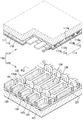
- 투명한 전면기판과 상기 전면기판과 대향하도록 배치되는 후면기판;상기 전면기판 및 후면기판 사이에 배치되고, 방전을 일으키는 공간인 복수의 방전셀들을 한정하도록 일 방향을 향해 구불구불하게 연장되어 배치되는 복수의 격벽들;전위가 인가되어 상기 방전셀 내에 전기장을 형성하는 복수의 전극들;상기 방전셀 내에 배치되는 형광체층; 및상기 방전셀 내에 존재하는 방전가스를 구비하고, 상기 격벽들이 연장되는 방향으로 서로 인접하는 방전셀들이 서로 어긋나도록 한정되는 것을 특징으로 하는 플라즈마 디스플레이 패널.
- 제 4 항에 있어서,상기 격벽들은 상기 격벽들 각각의 연장방향을 기준으로 좌우로 번갈아 어긋나도록 연장되는 것을 특징으로 하는 플라즈마 디스플레이 패널.
- 제 4 항에 있어서,상기 격벽은 상기 격벽이 연장되는 방향과 교차하는 방향으로 돌출되는 돌출부를 더 구비하는 것을 특징으로 하는 플라즈마 디스플레이 패널.
- 제 6 항에 있어서,상기 격벽의 돌출부는 상기 격벽이 한정하는 방전셀들의 내부를 향하도록 양방향으로 돌출되는 것을 특징으로 하는 플라즈마 디스플레이 패널.
- 제 4 항에 있어서,상기 격벽들 각각이 연장된 방향을 기준으로 인접한 방전셀들 사이에 방전이 일어나지 않는 공간인 비방전 영역이 형성되는 것을 특징으로 하는 플라즈마 디스플레이 패널.
- 제 8 항에 있어서,상기 비방전 영역을 한정하는 격벽의 부분에 홈이 형성되는 것을 특징으로 하는 플라즈마 디스플레이 패널.
- 제 4 항에 있어서,상기 전극들은 상기 격벽이 연장되는 방향과 교차하는 방향으로 연장되는 유지전극들과 상기 유지전극들과 상기 방전셀에서 교차하도록 연장되는 어드레스전극들을 구비하는 것을 특징으로 하는 플라즈마 디스플레이 패널.
- 제 10 항에 있어서,상기 유지전극들은 상기 전면기판에 지지되어 배치되고, 상기 유지전극들을 덮도록 상기 전면기판에 지지되어 배치되는 전방유전체층을 더 구비하는 것을 특징으로 하는 플라즈마 디스플레이 패널.
- 제 10 항 에 있어서,상기 어드레스전극들은 상기 후면기판에 지지되어 배치되는 것을 특징으로 하는 플라즈마 디스플레이 패널.
- 제 12 항 에 있어서,상기 어드레스전극들을 덮도록 상기 후면기판에 지지되어 배치되는 후방유전체층을 더 구비하는 것을 특징으로 하는 플라즈마 디스플레이 패널.
- 제 12 항 에 있어서,상기 어드레스전극들은 격벽들이 연장되는 방향을 따라 구불구불하게 연장되어 배치되는 것을 특징으로 하는 플라즈마 디스플레이 패널.
Priority Applications (4)
| Application Number | Priority Date | Filing Date | Title |
|---|---|---|---|
| KR1020050000798A KR100708658B1 (ko) | 2005-01-05 | 2005-01-05 | 플라즈마 디스플레이 패널 |
| US11/302,442 US7479737B2 (en) | 2005-01-05 | 2005-12-14 | Plasma display panel incorporating non-discharge areas between discharge cells |
| JP2006000145A JP2006190681A (ja) | 2005-01-05 | 2006-01-04 | プラズマディスプレイパネル |
| CNA2006100024957A CN1832088A (zh) | 2005-01-05 | 2006-01-05 | 等离子体显示面板 |
Applications Claiming Priority (1)
| Application Number | Priority Date | Filing Date | Title |
|---|---|---|---|
| KR1020050000798A KR100708658B1 (ko) | 2005-01-05 | 2005-01-05 | 플라즈마 디스플레이 패널 |
Publications (2)
| Publication Number | Publication Date |
|---|---|
| KR20060080413A KR20060080413A (ko) | 2006-07-10 |
| KR100708658B1 true KR100708658B1 (ko) | 2007-04-17 |
Family
ID=36639609
Family Applications (1)
| Application Number | Title | Priority Date | Filing Date |
|---|---|---|---|
| KR1020050000798A Expired - Fee Related KR100708658B1 (ko) | 2005-01-05 | 2005-01-05 | 플라즈마 디스플레이 패널 |
Country Status (4)
| Country | Link |
|---|---|
| US (1) | US7479737B2 (ko) |
| JP (1) | JP2006190681A (ko) |
| KR (1) | KR100708658B1 (ko) |
| CN (1) | CN1832088A (ko) |
Families Citing this family (3)
| Publication number | Priority date | Publication date | Assignee | Title |
|---|---|---|---|---|
| KR100777734B1 (ko) * | 2006-03-06 | 2007-11-19 | 삼성에스디아이 주식회사 | 플라즈마 디스플레이 패널 |
| KR20070097191A (ko) * | 2006-03-28 | 2007-10-04 | 삼성에스디아이 주식회사 | 플라즈마 디스플레이 패널 |
| JP2008091093A (ja) * | 2006-09-29 | 2008-04-17 | Fujitsu Hitachi Plasma Display Ltd | プラズマディスプレイパネル |
Citations (6)
| Publication number | Priority date | Publication date | Assignee | Title |
|---|---|---|---|---|
| KR19980083682A (ko) * | 1997-05-16 | 1998-12-05 | 구자홍 | 플라즈마 디스플레이 판넬 |
| KR19990056759A (ko) * | 1997-12-29 | 1999-07-15 | 김영환 | 플라즈마 디스플레이 패널 |
| KR100244132B1 (ko) | 1996-04-26 | 2000-02-01 | 김영남 | 플라즈마 표시소자 |
| JP2000311613A (ja) * | 1999-04-26 | 2000-11-07 | Hitachi Ltd | プラズマディスプレイパネル |
| JP2004039326A (ja) | 2002-07-01 | 2004-02-05 | Matsushita Electric Ind Co Ltd | プラズマディスプレイパネルおよびその製造方法 |
| JP2004152520A (ja) | 2002-10-29 | 2004-05-27 | Matsushita Electric Ind Co Ltd | プラズマディスプレイパネルの製造方法 |
Family Cites Families (19)
| Publication number | Priority date | Publication date | Assignee | Title |
|---|---|---|---|---|
| JP2917279B2 (ja) | 1988-11-30 | 1999-07-12 | 富士通株式会社 | ガス放電パネル |
| JP3259253B2 (ja) * | 1990-11-28 | 2002-02-25 | 富士通株式会社 | フラット型表示装置の階調駆動方法及び階調駆動装置 |
| US6097357A (en) * | 1990-11-28 | 2000-08-01 | Fujitsu Limited | Full color surface discharge type plasma display device |
| EP1231590A3 (en) * | 1991-12-20 | 2003-08-06 | Fujitsu Limited | Circuit for driving display panel |
| EP0554172B1 (en) * | 1992-01-28 | 1998-04-29 | Fujitsu Limited | Color surface discharge type plasma display device |
| JP3025598B2 (ja) * | 1993-04-30 | 2000-03-27 | 富士通株式会社 | 表示駆動装置及び表示駆動方法 |
| JP2891280B2 (ja) * | 1993-12-10 | 1999-05-17 | 富士通株式会社 | 平面表示装置の駆動装置及び駆動方法 |
| JP3719743B2 (ja) * | 1995-08-09 | 2005-11-24 | 株式会社日立製作所 | プラズマディスプレイパネル |
| JP3163563B2 (ja) * | 1995-08-25 | 2001-05-08 | 富士通株式会社 | 面放電型プラズマ・ディスプレイ・パネル及びその製造方法 |
| JP2845183B2 (ja) | 1995-10-20 | 1999-01-13 | 富士通株式会社 | ガス放電パネル |
| US6008582A (en) * | 1997-01-27 | 1999-12-28 | Dai Nippon Printing Co., Ltd. | Plasma display device with auxiliary partition walls, corrugated, tiered and pigmented walls |
| JP3424587B2 (ja) * | 1998-06-18 | 2003-07-07 | 富士通株式会社 | プラズマディスプレイパネルの駆動方法 |
| JP4030685B2 (ja) | 1999-07-30 | 2008-01-09 | 三星エスディアイ株式会社 | プラズマディスプレイおよびその製造方法 |
| JP2001325888A (ja) | 2000-03-09 | 2001-11-22 | Samsung Yokohama Research Institute Co Ltd | プラズマディスプレイ及びその製造方法 |
| KR100502330B1 (ko) * | 2000-04-29 | 2005-07-20 | 삼성에스디아이 주식회사 | 격벽이 마련된 기판 및 이를 이용한 플라즈마 표시장치 |
| JP3994626B2 (ja) | 2000-05-17 | 2007-10-24 | パイオニア株式会社 | プラズマディスプレイパネル |
| KR100402741B1 (ko) * | 2001-03-13 | 2003-10-17 | 삼성에스디아이 주식회사 | 기판 및 이 기판을 이용한 플라즈마 표시장치 |
| JP2003092064A (ja) * | 2001-09-18 | 2003-03-28 | Pioneer Electronic Corp | プラズマディスプレイパネル |
| KR100684791B1 (ko) * | 2005-04-08 | 2007-02-20 | 삼성에스디아이 주식회사 | 플라스마 표시 패널 |
-
2005
- 2005-01-05 KR KR1020050000798A patent/KR100708658B1/ko not_active Expired - Fee Related
- 2005-12-14 US US11/302,442 patent/US7479737B2/en not_active Expired - Fee Related
-
2006
- 2006-01-04 JP JP2006000145A patent/JP2006190681A/ja not_active Ceased
- 2006-01-05 CN CNA2006100024957A patent/CN1832088A/zh active Pending
Patent Citations (6)
| Publication number | Priority date | Publication date | Assignee | Title |
|---|---|---|---|---|
| KR100244132B1 (ko) | 1996-04-26 | 2000-02-01 | 김영남 | 플라즈마 표시소자 |
| KR19980083682A (ko) * | 1997-05-16 | 1998-12-05 | 구자홍 | 플라즈마 디스플레이 판넬 |
| KR19990056759A (ko) * | 1997-12-29 | 1999-07-15 | 김영환 | 플라즈마 디스플레이 패널 |
| JP2000311613A (ja) * | 1999-04-26 | 2000-11-07 | Hitachi Ltd | プラズマディスプレイパネル |
| JP2004039326A (ja) | 2002-07-01 | 2004-02-05 | Matsushita Electric Ind Co Ltd | プラズマディスプレイパネルおよびその製造方法 |
| JP2004152520A (ja) | 2002-10-29 | 2004-05-27 | Matsushita Electric Ind Co Ltd | プラズマディスプレイパネルの製造方法 |
Also Published As
| Publication number | Publication date |
|---|---|
| US20060145612A1 (en) | 2006-07-06 |
| JP2006190681A (ja) | 2006-07-20 |
| US7479737B2 (en) | 2009-01-20 |
| CN1832088A (zh) | 2006-09-13 |
| KR20060080413A (ko) | 2006-07-10 |
Similar Documents
| Publication | Publication Date | Title |
|---|---|---|
| US7750568B2 (en) | Plasma display panel (PDP) having a reflection preventive layer | |
| KR100708658B1 (ko) | 플라즈마 디스플레이 패널 | |
| US8120252B2 (en) | Plasma display panel | |
| US20060038492A1 (en) | Plasma display panel and method of fabricating the same | |
| US7557506B2 (en) | Plasma display panel | |
| EP1688982A2 (en) | Plasma display panel and manufacturing method thereof | |
| CN100521050C (zh) | 等离子体显示板 | |
| KR100696532B1 (ko) | 플라즈마 디스플레이 패널 및 표시 장치 | |
| KR20070107868A (ko) | 플라즈마 디스플레이 패널 | |
| KR20050112310A (ko) | 플라즈마 디스플레이 패널 | |
| KR100581941B1 (ko) | 플라즈마 디스플레이 패널 | |
| KR100670325B1 (ko) | 플라즈마 디스플레이 패널 | |
| KR100603377B1 (ko) | 플라즈마 디스플레이 패널 | |
| KR100592261B1 (ko) | 격벽의 구조가 개선된 플라즈마 디스플레이 패널 | |
| KR100626064B1 (ko) | 플라즈마 디스플레이 패널 | |
| KR100730211B1 (ko) | 플라즈마 디스플레이 패널 | |
| US20090021165A1 (en) | Plasma display panel and method of manufacturing the same | |
| KR100670315B1 (ko) | 플라즈마 디스플레이 패널 | |
| KR100708710B1 (ko) | 플라즈마 디스플레이 패널 | |
| KR100647620B1 (ko) | 플라즈마 디스플레이 패널 | |
| KR100573151B1 (ko) | 플라즈마 디스플레이 패널 | |
| JP2006216556A (ja) | プラズマディスプレイパネル | |
| KR100647617B1 (ko) | 플라즈마 디스플레이 패널 | |
| KR100670294B1 (ko) | 플라즈마 디스플레이 패널 | |
| KR100719536B1 (ko) | 플라즈마 디스플레이 패널 |
Legal Events
| Date | Code | Title | Description |
|---|---|---|---|
| A201 | Request for examination | ||
| PA0109 | Patent application |
Patent event code: PA01091R01D Comment text: Patent Application Patent event date: 20050105 |
|
| PA0201 | Request for examination | ||
| E902 | Notification of reason for refusal | ||
| PE0902 | Notice of grounds for rejection |
Comment text: Notification of reason for refusal Patent event date: 20060629 Patent event code: PE09021S01D |
|
| PG1501 | Laying open of application | ||
| E902 | Notification of reason for refusal | ||
| PE0902 | Notice of grounds for rejection |
Comment text: Notification of reason for refusal Patent event date: 20061227 Patent event code: PE09021S01D |
|
| E701 | Decision to grant or registration of patent right | ||
| PE0701 | Decision of registration |
Patent event code: PE07011S01D Comment text: Decision to Grant Registration Patent event date: 20070326 |
|
| GRNT | Written decision to grant | ||
| PR0701 | Registration of establishment |
Comment text: Registration of Establishment Patent event date: 20070411 Patent event code: PR07011E01D |
|
| PR1002 | Payment of registration fee |
Payment date: 20070412 End annual number: 3 Start annual number: 1 |
|
| PG1601 | Publication of registration | ||
| LAPS | Lapse due to unpaid annual fee | ||
| PC1903 | Unpaid annual fee |