KR100707087B1 - Manufacturing method of semiconductor device - Google Patents
Manufacturing method of semiconductor device Download PDFInfo
- Publication number
- KR100707087B1 KR100707087B1 KR1020010013584A KR20010013584A KR100707087B1 KR 100707087 B1 KR100707087 B1 KR 100707087B1 KR 1020010013584 A KR1020010013584 A KR 1020010013584A KR 20010013584 A KR20010013584 A KR 20010013584A KR 100707087 B1 KR100707087 B1 KR 100707087B1
- Authority
- KR
- South Korea
- Prior art keywords
- forming
- layer
- ion implantation
- single crystal
- vtn
- Prior art date
- Legal status (The legal status is an assumption and is not a legal conclusion. Google has not performed a legal analysis and makes no representation as to the accuracy of the status listed.)
- Expired - Fee Related
Links
Images


Classifications
-
- H—ELECTRICITY
- H10—SEMICONDUCTOR DEVICES; ELECTRIC SOLID-STATE DEVICES NOT OTHERWISE PROVIDED FOR
- H10D—INORGANIC ELECTRIC SEMICONDUCTOR DEVICES
- H10D30/00—Field-effect transistors [FET]
- H10D30/60—Insulated-gate field-effect transistors [IGFET]
- H10D30/67—Thin-film transistors [TFT]
- H10D30/6757—Thin-film transistors [TFT] characterised by the structure of the channel, e.g. transverse or longitudinal shape or doping profile
-
- H—ELECTRICITY
- H10—SEMICONDUCTOR DEVICES; ELECTRIC SOLID-STATE DEVICES NOT OTHERWISE PROVIDED FOR
- H10D—INORGANIC ELECTRIC SEMICONDUCTOR DEVICES
- H10D30/00—Field-effect transistors [FET]
- H10D30/60—Insulated-gate field-effect transistors [IGFET]
- H10D30/601—Insulated-gate field-effect transistors [IGFET] having lightly-doped drain or source extensions, e.g. LDD IGFETs or DDD IGFETs
Landscapes
- Insulated Gate Type Field-Effect Transistor (AREA)
- Thin Film Transistor (AREA)
Abstract
본 발명은 반도체소자의 제조방법에 관한 것으로, VTN/VTP 이온주입층(13)을 형성하는 과정과, Si 단결정층(14)을 형성하는 과정과, STI 개구패턴(11a)을 형성하는 과정과, STI 개구패턴(11a)이 매몰되도록 반도체기판(11)의 전면에 CVD 공정을 이용하여 산화막을 형성한 후 CMP 공정을 이용하여 Si 단결정층(14)이 드러나도록 산화막을 연마하여 STI 패턴(16)을 형성하는 과정과, 활성영역(A)의 소정 영역에 CVD 공정과 사진식각공정을 이용하여 게이트산화막(17)과 게이트전극(18)을 형성하고 이온주입공정을 이용하여 게이트전극(18)을 마스크로 사용하여 Si 단결정층(14)에 LDD층(19)을 형성하는 과정과, 게이트전극(18)의 측면에 CVD 공정을 이용하여 질화막을 형성한 후 사진식각공정을 이용하여 질화막을 식각하여 측벽(20)을 형성하고 이온주입공정을 이용하여 측벽(20)을 마스크로 사용하여 VTN/VTP 이온주입층(13)에 소스/드레인(S/D)을 형성하는 과정으로 구성하여, 채널을 매몰되도록 형성함으로써 전자가 표면과의 충돌로 인해 발생되는 저항을 제거하여 스위칭속도를 개선할 수 있도록 함에 있다. The present invention relates to a method for manufacturing a semiconductor device, comprising: forming a VTN / VTP ion implantation layer (13), forming a Si single crystal layer (14), forming a STI opening pattern (11a); After the oxide film is formed on the entire surface of the semiconductor substrate 11 so that the STI opening pattern 11a is buried, the oxide film is polished so that the Si single crystal layer 14 is exposed by using the CMP process. ), A gate oxide film 17 and a gate electrode 18 are formed in a predetermined region of the active region A using a CVD process and a photolithography process, and the gate electrode 18 using an ion implantation process. Is used as a mask to form the LDD layer 19 on the Si single crystal layer 14, the nitride film is formed on the side of the gate electrode 18 by a CVD process, and then the nitride film is etched using a photolithography process. To form the sidewall 20 and to finish the sidewall 20 using an ion implantation process. Forming a source / drain (S / D) in the VTN / VTP ion implantation layer 13 using a black, by forming a channel buried to remove the resistance caused by the collision of electrons with the surface switching To improve the speed.
반도체소자, STI, 채널, LDD, 결정성장 Semiconductor device, STI, channel, LDD, crystal growth
Description
도 1a 내지 도 1e는 종래의 반도체소자의 제조방법을 나타낸 반도체 기판의 단면도,1A to 1E are cross-sectional views of a semiconductor substrate showing a conventional method for manufacturing a semiconductor device;
도 2a 내지 도 2f는 본 발명에 의한 반도체소자의 제조방법을 나타낸 반도체기판의 단면도이다. 2A to 2F are cross-sectional views of a semiconductor substrate showing a method for manufacturing a semiconductor device according to the present invention.
<도면의 주요부분에 대한 부호설명><Code Description of Main Parts of Drawing>
11: 반도체기판 11a: STI 개구패턴 11:
12: 감광막패턴 13: VTN/VTP 이온주입층 12: Photoresist pattern 13: VTN / VTP ion implantation layer
14: Si 단결정층 15: STI 감광막패턴 14: Si single crystal layer 15: STI photosensitive film pattern
16: STI 패턴 17: 게이트산화막 16: STI Pattern 17: Gate Oxide
18: 게이트전극 19: LDD층 18: gate electrode 19: LDD layer
20: 측벽 21: 매몰채널
20: side wall 21: investment channel
본 발명은 반도체소자의 제조방법에 관한 것으로, 특히 저전압에서 동작이 가능하고 스위칭속도가 개선된 반도체소자의 매몰채널(buried channel)을 보다 용이하게 제조하기 위한 반도체소자의 제조방법에 관한 것이다. BACKGROUND OF THE
반도체소자의 표면 채널(surface channel)의 채널 길이의 물리적 한계, 스위칭속도 및 동작전압을 개선하기 위해 매몰채널(buried channel)이 개발되었다. 매몰채널이 적용된 종래의 반도체소자의 제조방법을 첨부된 도면을 이용하여 설명하면 다음과 같다. Buried channels have been developed to improve the physical limits of the channel length, switching speed and operating voltage of the surface channels of semiconductor devices. Hereinafter, a method of manufacturing a conventional semiconductor device to which an investment channel is applied will be described with reference to the accompanying drawings.
도 1a 내지 도 1e는 종래의 반도체소자의 제조방법을 나타낸 반도체기판의 단면도이다. 먼저, 도 1a에서와 같이 반도체 기판(1)에 사진공정을 이용하여 활성영역(A)과 비활성영역(B)을 정의하기 위한 STI(shallow trench isolation) 감광막패턴(2)을 형성한다. STI 감광막패턴(2)이 형성되면 도 1b에서와 같이 STI 감광막패턴(2)을 식각마스크로 이용하여 반도체기판(1)을 소정 깊이로 식각하여 STI 개구패턴(1a)을 형성한다. 1A to 1E are cross-sectional views of a semiconductor substrate showing a conventional method for manufacturing a semiconductor device. First, as shown in FIG. 1A, a shallow trench isolation (STI)
STI 개구패턴(1a)을 형성한 후에 도 1c에서와 같이, STI 개구패턴(1a)이 매몰되도록 반도체기판(1)의 전면에 CVD(chemical vapor deposition) 공정을 이용하여 산화막을 형성한 후 CMP(chemical mechanical polishing) 공정을 이용하여 활성영역(A)이 드러나도록 산화막을 연마하여 STI 패턴(3)을 형성한다.
After the
비활성영역(B)에 STI 패턴(3)이 형성되면 도 1d에서와 같이 활성영역(A)에 이온주입공정(도시 않음)을 이용하여 반도체소자의 문턱전압을 조절하기 위한 이온(이하 VTN 또는 VTP 이온이라 약칭함)을 주입하여 VTN/VTP 이온주입층(4)을 형성한다. VTN/VTP 이온주입층(4)을 형성한 후 도 1e에서와 같이 VTN/VTP 이온주입층(4)의 소정의 영역에 게이트산화막(5)과 게이트전극(6)을 형성하고, 이온주입공정을 이용하여 게이트전극(6)을 마스크로 사용하여 VTN/VTP 이온주입층(4)에 LDD(lightly doped drain)층(8)을 형성한다. When the
LDD(lightly doped drain)층(8)이 형성되면 게이트전극(6)의 측면에 CVD 공정을 이용하여 질화막을 형성한 후 사진식각공정을 이용하여 질화막을 식각하여 측벽(sidewall)(7)을 형성한다. 측벽(7)이 형성되면 이온주입공정을 이용하여 측벽(7)을 마스크로 사용하여 소스/드레인(S/D)을 형성한다. 소스/드레인(S/D)이 형성되면 LDD층(8) 사이에 표면채널(surface channel)(9)을 갖는 반도체소자의 제조가 완료된다. When the LDD (lightly doped drain)
이상과 같이 종래의 표면채널(surface channel)이 적용된 반도체소자는 채널의 길이를 짧게 형성하는 것이 불가능하며, 소스에서 드레인으로 전자의 이동시 채널과 게이트산화막의 계면과의 충돌로 인한 저항이 발생되어 스위칭속도가 저하되는 문제점이 있다. As described above, in the semiconductor device to which the conventional surface channel is applied, it is impossible to form a short channel length, and when the electrons move from the source to the drain, resistance due to the collision between the interface of the channel and the gate oxide film is generated and switched. There is a problem that the speed is lowered.
본 발명의 목적은 매몰채널을 갖는 반도체소자의 제조 공정에서 매몰채널의 이온주입공정을 진행한 후 Si 단결정을 성장시켜 매몰채널의 깊이를 용이하게 조절 함과 아울러 스위칭속도를 개선한 매몰채널을 갖는 반도체소자의 제조방법을 제공함에 있다. An object of the present invention is to increase the depth of the buried channel by growing the Si single crystal after the ion implantation process of the buried channel in the manufacturing process of the semiconductor device having the buried channel and having a buried channel with improved switching speed The present invention provides a method for manufacturing a semiconductor device.
본 발명의 다른 목적은 매몰채널을 갖는 반도체소자에서 매몰채널의 깊이를 용이하게 조절할 수 있도록 함으로써 반도체소자를 보다 용이하게 제조하여 생산성을 향상시킴에 있다. Another object of the present invention is to improve the productivity by making the semiconductor device easier by making it possible to easily control the depth of the buried channel in the semiconductor device having a buried channel.
본 발명의 반도체소자 제조방법은 반도체기판의 표면에 활성영역과 비활성영역을 정의하고 비활성영역에 감광막패턴을 형성한 후 감광막패턴을 마스크로 하여 활성영역에 VTN 또는 VTP 이온을 주입하여 VTN/VTP 이온주입층을 형성하는 과정; 결정성장공정을 이용하여 반도체기판의 전면에 소정의 두께를 갖는 Si 단결정층을 형성하는 과정; Si 단결정층이 형성된 활성영역 위에 사진식각 공정을 이용하여 STI 감광막패턴을 형성하고 STI 감광막패턴을 식각마스크로 이용하여 Si 단결정층과 반도체기판을 순차적으로 식각하여 STI 개구패턴을 형성하는 과정; STI 개구패턴이 매몰되도록 반도체기판의 전면에 CVD 공정을 이용하여 산화막을 형성한 후 CMP 공정을 이용하여 Si 단결정층이 드러나도록 산화막을 연마하여 STI 패턴을 형성하는 과정; 활성영역의 소정 영역에 CVD 공정과 사진식각공정을 이용하여 게이트산화막과 게이트전극을 형성하고 이온주입공정을 이용하여 게이트전극을 마스크로 사용하여 Si 단결정층에 LDD층을 형성하는 과정; 및 게이트전극의 측면에 CVD 공정을 이용하여 질화막을 형성한 후 사진식각공정을 이용하여 질화막을 식각하여 측벽을 형성하고 이온주입공정을 이용하여 측벽을 마스크로 사용하여 VTN/VTP 이온주입층에 소스/드레인을 형성하는 과정으로 구성됨을 특징으로 한다.The semiconductor device manufacturing method of the present invention defines an active region and an inactive region on the surface of the semiconductor substrate, forms a photoresist pattern on the inactive region, and then injects VTN or VTP ions into the active region using the photoresist pattern as a mask. Forming an injection layer; Forming a Si single crystal layer having a predetermined thickness on the entire surface of the semiconductor substrate by using a crystal growth process; Forming an STI photoresist pattern on the active region on which the Si single crystal layer is formed by using a photolithography process and sequentially etching the Si single crystal layer and the semiconductor substrate using the STI photoresist pattern as an etching mask; Forming an oxide film on the entire surface of the semiconductor substrate using the CVD process so that the STI opening pattern is buried, and then polishing the oxide film to expose the Si single crystal layer using the CMP process to form an STI pattern; Forming a gate oxide film and a gate electrode in a predetermined region of the active region by using a CVD process and a photolithography process and forming an LDD layer on the Si single crystal layer using the gate electrode as a mask using an ion implantation process; After the nitride film is formed on the side of the gate electrode by using a CVD process, the nitride film is etched by using a photolithography process to form sidewalls, and the sidewall is used as a mask by using an ion implantation process. / Drain forming process.
VTN/VTP 이온주입층을 형성하는 과정에서 VTN 이온은 B 및 BF2 중 어느 하나가 선택되어 주입됨을 특징으로 하며, VTN/VTP 이온주입층을 형성하는 과정에서 VTP 이온은 As 및 P 중 어느 하나가 선택되어 주입됨을 특징으로 하고, 게이트산화막과 게이트전극과 LDD층을 형성하는 과정에서 게이트산화막은 열산화막으로 형성됨을 특징으로 한다.In the process of forming the VTN / VTP ion implantation layer, the VTN ions are selected by implanting any one of B and BF 2 , and in the process of forming the VTN / VTP ion implantation layer, the VTP ions are either As and P Is selected and implanted, and in the process of forming the gate oxide film, the gate electrode, and the LDD layer, the gate oxide film is formed of a thermal oxide film.
본 발명의 구성 및 작용을 보다 상세히 설명하면 다음과 같다.Referring to the configuration and operation of the present invention in more detail as follows.
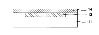
도 2a 내지 도 2f는 본 발명에 의한 반도체소자의 제조방법을 나타낸 반도체기판의 단면도이다. 도시된 바와 같이, 반도체기판(11)의 표면에 활성영역(A)과 비활성영역(B)을 정의하고 비활성영역(B)에 감광막패턴(12)을 형성한 후 감광막패턴(12)을 마스크로 하여 활성영역(A)에 VTN 또는 VTP 이온을 주입하여 VTN/VTP 이온주입층(13)을 형성하는 과정과, 결정성장공정을 이용하여 반도체기판(11)의 전면에 소정의 두께를 갖는 Si 단결정층(14)을 형성하는 과정과, Si 단결정층(14)이 형성된 활성영역(A) 위에 사진식각 공정을 이용하여 STI 감광막패턴(15)을 형성하고 STI 감광막패턴(15)을 식각마스크로 이용하여 Si 단결정층(14)과 반도체기판(11)을 순차적으로 식각하여 STI 개구패턴(11a)을 형성하는 과정과, STI 개구패턴(11a)이 매몰되도록 반도체기판(11)의 전면에 CVD 공정을 이용하여 산화막을 형성한 후 CMP 공정을 이용하여 Si 단결정층(14)이 드러나도록 산화막을 연마하여 STI 패턴(16)을 형성하는 과정과, 활성영역(A)의 소정 영역에 CVD 공정과 사진식각공정을 이용하여 게이트산화막(17)과 게이트전극(18)을 형성하고 이온주입공정을 이용하여 게이트전극(18)을 마스크로 사용하여 Si 단결정층(14)에 LDD층(19)을 형성하는 과정과, 게이트전극(18)의 측면에 CVD 공정을 이용하여 질화막을 형성한 후 사진식각공정을 이용하여 질화막을 식각하여 측벽(20)을 형성하고 이온주입공정을 이용하여 측벽(20)을 마스크로 사용하여 VTN/VTP 이온주입층(13)에 소스/드레인(S/D)을 형성하는 과정으로 구성된다. 2A to 2F are cross-sectional views of a semiconductor substrate showing a method for manufacturing a semiconductor device according to the present invention. As illustrated, the active region A and the inactive region B are defined on the surface of the
본 발명의 구성 및 작용을 보다 상세히 설명하면 다음과 같다.Referring to the configuration and operation of the present invention in more detail as follows.
본 발명의 매몰채널(21)을 갖는 반도체소자를 제조하기 위해 먼저 도 2a에서와 같이 반도체기판(11)의 표면에 활성영역(A)과 비활성영역(B)을 정의하고 비활성영역(B)에 감광막패턴(12)을 형성한 후 감광막패턴(12)을 마스크로 하여 활성영역(A)에 VTN 또는 VTP 이온을 주입하여 VTN/VTP 이온주입층(13)을 형성하는 과정을 실시한다. VTN/VTP 이온주입층(13)을 형성하는 과정에서 VTN 이온은 B 및 BF2 중 어느 하나가 선택되어 주입되며, VTP 이온은 As 및 P 중 어느 하나가 선택되어 주입된다. 여기서, VTN 또는 VTP 이온은 N 채널 모스소자(MOSFET)나 P채널 모스소자(MOSFET)를 형성하거나 씨모스소자(CMOS FET)를 형성시 소자의 문턱전압을 조절하기 위한 소스이다.In order to manufacture the semiconductor device having the buried
VTN/VTP 이온주입층(13)이 형성되면 도 2b에서와 같이 결정성장공정을 이용하여 반도체기판(11)의 전면에 소정의 두께를 갖는 Si 단결정층(14)을 형성하는 과정이 실시된다. Si 단결정층(14)은 반도체기판(11)이 실리콘웨이퍼가 사용되는 경 우에 결정성장공정을 이용하여 실리콘웨이퍼의 결정방향으로 Si 결정을 성장시킨다. When the VTN / VTP
반도체기판(11)의 표면에 Si 단결정층(14)이 소정의 두께로 성장되면 도 2c 및 도 2d에서와 같이 Si 단결정층(14)이 형성된 활성영역(A) 위에 사진식각 공정을 이용하여 STI 감광막패턴(15)을 형성하고 STI 감광막패턴(15)을 식각마스크로 이용하여 Si 단결정층(14)과 반도체기판(11)을 순차적으로 식각하여 STI 개구패턴(11a)을 형성하는 과정이 실시된다. When the Si
STI 개구패턴(11a)을 형성하기 위해 먼저 도 2c에서와 같이 활성영역(A)에 형성된 Si 단결정층(14) 위에 감광막을 도포한 후 감광막을 사진식각공정을 이용하여 STI 감광막패턴(15)을 형성한다. STI 감광막패턴(15)이 형성되면 도 2d에서와 같이 STI 감광막패턴(15)을 식각마스크로 하여 Si 단결정층(14)과 반도체기판(11)을 순차적으로 식각한다. Si 단결정층(14)의 식각시 Si 단결정층(14)이 관통되도록 식각되며, Si 단결정층(14)이 완전히 식각되어 관통되면 반도체기판(11)을 소정 깊이로 식각하여 비활성영역(B)에 STI 개구패턴(11a)을 형성한다. In order to form the
비활성영역(B)에 STI 개구패턴(11a)이 형성되면 도 2e에서와 같이 STI 개구패턴(11a)이 매몰되도록 반도체기판(11)의 전면에 CVD 공정을 이용하여 산화막을 형성한 후 CMP 공정을 이용하여 Si 단결정층(14)이 드러나도록 산화막을 연마하여 STI 패턴(16)을 형성하는 과정이 실시된다. When the
STI 패턴(16)이 형성되면 도 2f에서와 같이 활성영역(A)의 소정 영역에 CVD 공정과 사진식각공정을 이용하여 게이트산화막(17)과 게이트전극(18)을 형성하고 이온주입공정을 이용하여 게이트전극(18)을 마스크로 사용하여 Si 단결정층(14)에 LDD층(19)을 형성하는 과정이 실시된다. 여기서, 게이트산화막(17)은 열산화막으로 형성된다. When the
게이트산화막(17)과 게이트전극(18)과 LDD층(19)이 형성되면 게이트전극(18)의 측면에 CVD 공정을 이용하여 질화막을 형성한 후 사진식각공정을 이용하여 질화막을 식각하여 측벽(20)을 형성하고 이온주입공정을 이용하여 측벽(20)을 마스크로 사용하여 VTN/VTP 이온주입층(13)에 소스/드레인(S/D)을 형성하는 과정이 실시된다. 측벽(20)의 식각시 등방성 식각하며, 측벽(20)의 식각공정이 완료되면 측벽(20)을 마스크로 하여 VTN/VTP 이온주입층(13)에 이온을 주입하여 소스/드레인(S/D)이 형성되면 소스/드레인(S/D) 사이에 매몰채널(21)이 형성된다. When the
이상과 같이 VTN/VTP 이온주입층에 채널을 형성함으로써 VTN/VTP 이온주입층의 확산 깊이 조절에 의해 매몰채널의 깊이를 조절할 수 있도록 함으로써 매몰채널의 깊이를 용이하게 조절할 수 있고, 채널을 매몰되도록 형성함으로써 전자가 표면과의 충돌로 인해 발생되는 저항을 제거하여 스위칭속도를 개선할 수 있게 된다. As described above, by forming a channel in the VTN / VTP ion implantation layer, the depth of the buried channel can be easily adjusted by controlling the depth of diffusion of the VTN / VTP ion implantation layer, and the channel is buried. By forming the electrons, the switching speed can be improved by removing the resistance caused by the collision with the surface of the electrons.
이상에서 설명한 바와 같이 본 발명은 채널을 매몰되도록 형성함으로써 전자가 표면과의 충돌로 인해 발생되는 저항을 제거하여 스위칭속도를 개선할 수 있으며, VTN/VTP 이온주입층의 확산 깊이 조절에 의해 매몰채널의 깊이를 조절할 수 있도록 함으로써 매몰채널의 깊이를 용이하게 조절할 수 있어 반도체소자의 생산성을 향상시킬 수 있는 효과를 제공한다.As described above, the present invention can improve the switching speed by removing the resistance generated due to the collision of electrons with the surface by forming the channel buried, and the buried channel by controlling the depth of diffusion of the VTN / VTP ion implantation layer. By controlling the depth of the buried channel can be easily adjusted to provide the effect of improving the productivity of the semiconductor device.
Claims (4)
Priority Applications (1)
| Application Number | Priority Date | Filing Date | Title |
|---|---|---|---|
| KR1020010013584A KR100707087B1 (en) | 2001-03-16 | 2001-03-16 | Manufacturing method of semiconductor device |
Applications Claiming Priority (1)
| Application Number | Priority Date | Filing Date | Title |
|---|---|---|---|
| KR1020010013584A KR100707087B1 (en) | 2001-03-16 | 2001-03-16 | Manufacturing method of semiconductor device |
Publications (2)
| Publication Number | Publication Date |
|---|---|
| KR20020073773A KR20020073773A (en) | 2002-09-28 |
| KR100707087B1 true KR100707087B1 (en) | 2007-04-13 |
Family
ID=27697598
Family Applications (1)
| Application Number | Title | Priority Date | Filing Date |
|---|---|---|---|
| KR1020010013584A Expired - Fee Related KR100707087B1 (en) | 2001-03-16 | 2001-03-16 | Manufacturing method of semiconductor device |
Country Status (1)
| Country | Link |
|---|---|
| KR (1) | KR100707087B1 (en) |
Families Citing this family (1)
| Publication number | Priority date | Publication date | Assignee | Title |
|---|---|---|---|---|
| KR20030053958A (en) * | 2001-12-24 | 2003-07-02 | 동부전자 주식회사 | a method for manufacturing of transistor of semiconductor device |
Citations (4)
| Publication number | Priority date | Publication date | Assignee | Title |
|---|---|---|---|---|
| KR970053015A (en) * | 1995-12-07 | 1997-07-29 | 김주용 | Transistor manufacturing method of semiconductor device |
| KR19990033123A (en) * | 1997-10-23 | 1999-05-15 | 구본준 | Semiconductor element and manufacturing method thereof |
| KR100237180B1 (en) * | 1997-05-16 | 2000-01-15 | 정선종 | Configuration of mos transistor |
| US6064077A (en) * | 1991-08-30 | 2000-05-16 | Stmicroelectronics, Inc. | Integrated circuit transistor |
-
2001
- 2001-03-16 KR KR1020010013584A patent/KR100707087B1/en not_active Expired - Fee Related
Patent Citations (4)
| Publication number | Priority date | Publication date | Assignee | Title |
|---|---|---|---|---|
| US6064077A (en) * | 1991-08-30 | 2000-05-16 | Stmicroelectronics, Inc. | Integrated circuit transistor |
| KR970053015A (en) * | 1995-12-07 | 1997-07-29 | 김주용 | Transistor manufacturing method of semiconductor device |
| KR100237180B1 (en) * | 1997-05-16 | 2000-01-15 | 정선종 | Configuration of mos transistor |
| KR19990033123A (en) * | 1997-10-23 | 1999-05-15 | 구본준 | Semiconductor element and manufacturing method thereof |
Also Published As
| Publication number | Publication date |
|---|---|
| KR20020073773A (en) | 2002-09-28 |
Similar Documents
| Publication | Publication Date | Title |
|---|---|---|
| US6153455A (en) | Method of fabricating ultra shallow junction CMOS transistors with nitride disposable spacer | |
| US5918129A (en) | Method of channel doping using diffusion from implanted polysilicon | |
| US6191446B1 (en) | Formation and control of a vertically oriented transistor channel length | |
| KR0165457B1 (en) | Trench element isolation | |
| US7052965B2 (en) | Methods of fabricating MOS field effect transistors with pocket regions using implant blocking patterns | |
| US6069384A (en) | Integrated circuit including vertical transistors with spacer gates having selected gate widths | |
| US7217625B2 (en) | Method of fabricating a semiconductor device having a shallow source/drain region | |
| KR100840661B1 (en) | Semiconductor device and manufacturing method thereof | |
| KR100707087B1 (en) | Manufacturing method of semiconductor device | |
| KR100282453B1 (en) | Method for manufacturing semiconductor device the same | |
| KR100320436B1 (en) | Method for manufacturing mosfet | |
| KR100386610B1 (en) | Semiconductor device and method for manufacturing the same | |
| KR100597462B1 (en) | Method for fabricating transistor of semiconductor device | |
| KR100485004B1 (en) | Soi semiconductor device and method for manufacturing the same | |
| KR20030059391A (en) | Method of manufacturing semiconductor device | |
| KR20000003936A (en) | Transistor of semiconductor devices and method thereof | |
| KR100520512B1 (en) | Method for manufacturing semiconductor device with nitrogen implant | |
| KR100324339B1 (en) | Fabricating method of semiconductor device | |
| KR20020002918A (en) | Method for fabricating transistor of semiconductor memory device | |
| KR100308783B1 (en) | Semiconductor device manufacturing method | |
| KR100348314B1 (en) | Semiconductor device and method for fabricating the same | |
| KR100940113B1 (en) | High voltage transistor manufacturing method | |
| KR100460756B1 (en) | Method of manufacturing semiconductor device | |
| KR100469333B1 (en) | Method of manufacturing a semiconductor device | |
| KR20020056259A (en) | Method for forming transistor in semiconductor device |
Legal Events
| Date | Code | Title | Description |
|---|---|---|---|
| PA0109 | Patent application |
St.27 status event code: A-0-1-A10-A12-nap-PA0109 |
|
| R18-X000 | Changes to party contact information recorded |
St.27 status event code: A-3-3-R10-R18-oth-X000 |
|
| R17-X000 | Change to representative recorded |
St.27 status event code: A-3-3-R10-R17-oth-X000 |
|
| P11-X000 | Amendment of application requested |
St.27 status event code: A-2-2-P10-P11-nap-X000 |
|
| P13-X000 | Application amended |
St.27 status event code: A-2-2-P10-P13-nap-X000 |
|
| PG1501 | Laying open of application |
St.27 status event code: A-1-1-Q10-Q12-nap-PG1501 |
|
| R18-X000 | Changes to party contact information recorded |
St.27 status event code: A-3-3-R10-R18-oth-X000 |
|
| A201 | Request for examination | ||
| PA0201 | Request for examination |
St.27 status event code: A-1-2-D10-D11-exm-PA0201 |
|
| PN2301 | Change of applicant |
St.27 status event code: A-3-3-R10-R13-asn-PN2301 St.27 status event code: A-3-3-R10-R11-asn-PN2301 |
|
| PN2301 | Change of applicant |
St.27 status event code: A-3-3-R10-R13-asn-PN2301 St.27 status event code: A-3-3-R10-R11-asn-PN2301 |
|
| R17-X000 | Change to representative recorded |
St.27 status event code: A-3-3-R10-R17-oth-X000 |
|
| D13-X000 | Search requested |
St.27 status event code: A-1-2-D10-D13-srh-X000 |
|
| D14-X000 | Search report completed |
St.27 status event code: A-1-2-D10-D14-srh-X000 |
|
| E701 | Decision to grant or registration of patent right | ||
| PE0701 | Decision of registration |
St.27 status event code: A-1-2-D10-D22-exm-PE0701 |
|
| GRNT | Written decision to grant | ||
| PR0701 | Registration of establishment |
St.27 status event code: A-2-4-F10-F11-exm-PR0701 |
|
| PR1002 | Payment of registration fee |
St.27 status event code: A-2-2-U10-U11-oth-PR1002 Fee payment year number: 1 |
|
| PG1601 | Publication of registration |
St.27 status event code: A-4-4-Q10-Q13-nap-PG1601 |
|
| PR1001 | Payment of annual fee |
St.27 status event code: A-4-4-U10-U11-oth-PR1001 Fee payment year number: 4 |
|
| PR1001 | Payment of annual fee |
St.27 status event code: A-4-4-U10-U11-oth-PR1001 Fee payment year number: 5 |
|
| FPAY | Annual fee payment |
Payment date: 20120319 Year of fee payment: 6 |
|
| PR1001 | Payment of annual fee |
St.27 status event code: A-4-4-U10-U11-oth-PR1001 Fee payment year number: 6 |
|
| LAPS | Lapse due to unpaid annual fee | ||
| PC1903 | Unpaid annual fee |
St.27 status event code: A-4-4-U10-U13-oth-PC1903 Not in force date: 20130406 Payment event data comment text: Termination Category : DEFAULT_OF_REGISTRATION_FEE |
|
| PC1903 | Unpaid annual fee |
St.27 status event code: N-4-6-H10-H13-oth-PC1903 Ip right cessation event data comment text: Termination Category : DEFAULT_OF_REGISTRATION_FEE Not in force date: 20130406 |
|
| P22-X000 | Classification modified |
St.27 status event code: A-4-4-P10-P22-nap-X000 |
|
| P22-X000 | Classification modified |
St.27 status event code: A-4-4-P10-P22-nap-X000 |