KR100702364B1 - MTC MOS Latch Circuit - Google Patents
MTC MOS Latch Circuit Download PDFInfo
- Publication number
- KR100702364B1 KR100702364B1 KR1020060060355A KR20060060355A KR100702364B1 KR 100702364 B1 KR100702364 B1 KR 100702364B1 KR 1020060060355 A KR1020060060355 A KR 1020060060355A KR 20060060355 A KR20060060355 A KR 20060060355A KR 100702364 B1 KR100702364 B1 KR 100702364B1
- Authority
- KR
- South Korea
- Prior art keywords
- signal
- gate
- circuit unit
- control
- sleep
- Prior art date
- Legal status (The legal status is an assumption and is not a legal conclusion. Google has not performed a legal analysis and makes no representation as to the accuracy of the status listed.)
- Expired - Fee Related
Links
Images


Classifications
-
- H—ELECTRICITY
- H03—ELECTRONIC CIRCUITRY
- H03K—PULSE TECHNIQUE
- H03K3/00—Circuits for generating electric pulses; Monostable, bistable or multistable circuits
- H03K3/02—Generators characterised by the type of circuit or by the means used for producing pulses
- H03K3/027—Generators characterised by the type of circuit or by the means used for producing pulses by the use of logic circuits, with internal or external positive feedback
- H03K3/037—Bistable circuits
- H03K3/0375—Bistable circuits provided with means for increasing reliability; for protection; for ensuring a predetermined initial state when the supply voltage has been applied; for storing the actual state when the supply voltage fails
-
- H—ELECTRICITY
- H03—ELECTRONIC CIRCUITRY
- H03K—PULSE TECHNIQUE
- H03K3/00—Circuits for generating electric pulses; Monostable, bistable or multistable circuits
- H03K3/01—Details
- H03K3/012—Modifications of generator to improve response time or to decrease power consumption
-
- H—ELECTRICITY
- H03—ELECTRONIC CIRCUITRY
- H03K—PULSE TECHNIQUE
- H03K3/00—Circuits for generating electric pulses; Monostable, bistable or multistable circuits
- H03K3/02—Generators characterised by the type of circuit or by the means used for producing pulses
- H03K3/353—Generators characterised by the type of circuit or by the means used for producing pulses by the use, as active elements, of field-effect transistors with internal or external positive feedback
- H03K3/356—Bistable circuits
- H03K3/356104—Bistable circuits using complementary field-effect transistors
- H03K3/356113—Bistable circuits using complementary field-effect transistors using additional transistors in the input circuit
- H03K3/356121—Bistable circuits using complementary field-effect transistors using additional transistors in the input circuit with synchronous operation
Landscapes
- Logic Circuits (AREA)
Abstract
본 발명은 슬립제어 신호(SLP)의 제어하에 입력 데이터를 반전시켜 출력하는 데이터 반전 회로부, 상기 데이터 반전 회로부에서 출력되는 데이터 신호를 클럭 제어 신호(CLK)의 제어에 의해 전달하는 전달 게이트, 상기 전달 게이트에서 출력되는 데이터 신호를 리셋 제어 신호(RS)와 슬립 제어 신호(SLP)의 제어에 의해 출력하는 신호 제어 회로부, 상기 신호 제어 회로부에서 출력되는 신호를 피드백하여 슬립 모드시에 데이터를 보전하는 피드백 회로부로 구성된 것으로서, 소자의 기술이 나노급으로 스케링됨에 따라 누설전류에 의한 전력소모를 최소화시킬 뿐만 아니라 낮은 문턱 전압을 갖는 소자의 사용으로 인해 로직 회로의 고속동작에도 크게 기여할 수 있다.The present invention provides a data inversion circuit unit for inverting and outputting input data under the control of a slip control signal SLP, a transfer gate for transmitting a data signal output from the data inversion circuit unit under control of a clock control signal CLK, and the transfer. A signal control circuit unit for outputting the data signal output from the gate by the control of the reset control signal RS and the sleep control signal SLP, and a feedback for preserving data in the sleep mode by feeding back the signal output from the signal control circuit unit. It is composed of a circuit part, and as the technology of the device is nano-scaled, it not only minimizes power consumption due to leakage current but also contributes to high speed operation of logic circuit due to the use of a device having a low threshold voltage.
래치회로, MTCMOS, 다중문턱, 슬립모드 Latch Circuit, MTCMOS, Multi-Threshold, Sleep Mode
Description
도 1은 종래의 단일 문턱 전압을 이용한 래치 회로를 나타낸 도면.1 illustrates a latch circuit using a conventional single threshold voltage.
도 2는 종래의 클럭 신호 발생 회로를 나타낸 도면.2 is a view showing a conventional clock signal generation circuit.
도 3a 내지 도 3c는 도 1의 회로에 도시된 소자들을 등가의 트랜지스터로 나타낸 도면.3A-3C show equivalent transistors of the elements shown in the circuit of FIG.
도 4는 본 발명에 따른 MTCMOS 래치회로를 나타난 도면.4 illustrates an MTCMOS latch circuit in accordance with the present invention.
도 5는 본 발명에 따른 슬립 신호 발생 회로를 나타낸 도면.5 illustrates a sleep signal generation circuit according to the present invention;
도 6은 본 발명에 따른 클럭 신호 발생 회로를 나타낸 도면.6 illustrates a clock signal generation circuit in accordance with the present invention.
도 7a 내지 도 7e는 도 4에 도시된 MTCMOS 래치회로내의 개별 회로도를 나타낸 도면.7A-7E are individual circuit diagrams in the MTCMOS latch circuit shown in FIG.
도 8은 본 발명에 따른 MTCMOS 래치회로의 신호 동작 타이밍도. 8 is a signal operation timing diagram of an MTCMOS latch circuit according to the present invention;
도 9는 본 발명의 다른 실시예에 따른 MTCMOS 래치회로를 나타낸 도면. 9 illustrates an MTCMOS latch circuit according to another embodiment of the present invention.
<도면의 주요 부분에 대한 부호의 설명><Explanation of symbols for the main parts of the drawings>
400, 900 : 데이터 반전 회로부 400, 900: data inversion circuit
402,432, 500, 510, 600, 610, 902, 932 : 인버터402,432, 500, 510, 600, 610, 902, 932: Inverter
410, 910 : 전달 게이트 420, 920 : 신호 제어 회로부410, 910:
422, 922 : NOR 게이트 430, 930 : 피드백 회로부422, 922: NOR
434 : 피드백 전달 게이트434: feedback transfer gate
본 발명은 MTCMOS(Multi-Threshold CMOS) 기술을 이용하여 슬립 모드에서 누설 전류 없이 데이터를 보전할 수 있는 MTCMOS(Multi-Threshold CMOS) 래치 회로에 관한 것이다. The present invention relates to a multi-threshold CMOS (MTCMOS) latch circuit capable of preserving data without leakage current in a sleep mode using multi-threshold CMOS (MTCMOS) technology.
래치 회로는 하나의 데이터 입력, 하나의 클럭 입력 그리고 하나의 출력을 갖는다. 클럭 입력이 활성화되면, 입력되고 있는 데이터가 입수되어 출력측으로 전달되고, 클럭 입력이 비활성화될 때 데이터는 피드백회로내에 보전된다.The latch circuit has one data input, one clock input and one output. When the clock input is activated, the data being input is obtained and delivered to the output side, and the data is retained in the feedback circuit when the clock input is deactivated.
도 1은 종래의 단일 문턱 전압을 이용한 래치 회로를 나타낸 도면, 도 2는 종래의 클럭 신호 발생 회로를 나타낸 도면, 도 3a 내지 도 3c는 도 1의 회로에 도시된 소자들을 등가의 트랜지스터로 나타낸 도면이다.1 is a diagram illustrating a conventional latch circuit using a single threshold voltage, FIG. 2 is a diagram illustrating a conventional clock signal generation circuit, and FIGS. 3A to 3C are diagrams illustrating elements shown in the circuit of FIG. 1 as equivalent transistors. to be.
도 1 내지 도 3c를 참조하면, 단일 문턱 전압을 이용한 래치 회로는 클럭신호(CP)와 반전 클럭신호(CPb)에 의해 제어되는 전달 게이트(100), 리셋 제어 신호(RS)에 의해 데이터(D)를 출력하는 낸드 게이트(110), 상기 낸드 게이트(110)에서 출력되는 신호를 반전시키는 인버터 1(120), 피드백 전달게이트(130)를 포함한 다.1 to 3C, a latch circuit using a single threshold voltage includes data D by a
상기 클럭신호(CP)와 반전 클럭신호(CPb)는 도 2와 같은 클럭 신호 발생 회로에 의해 발생된다. 상기 클럭 신호 발생 회로는 인버터 2(210)와 인버터 3(220)로 구성된다. The clock signal CP and the inverted clock signal CPb are generated by a clock signal generation circuit as shown in FIG. 2. The clock signal generation circuit includes an inverter 2 210 and an inverter 3 220.
따라서, high 상태의 클럭 제어 신호(CLK)가 입력되면, 상기 인버터 2(210)에 의해 low 상태의 반전 클럭 신호(CPb)가 출력되고, 상기 인버터2 및 3(210, 220)에 의해 high 상태의 클럭신호(CP)가 출력된다. 또한, low 상태의 클럭 제어 신호(CLK)가 입력되면, 상기 인버터 2(210)에 의해 high 상태의 반전 클럭 신호(CPb)가 출력되고, 상기 인버터 2 및 3(210, 220)에 의해 low 상태의 클럭신호(CP)가 출력된다.Accordingly, when the clock control signal CLK in the high state is input, the inverted clock signal CPb in the low state is output by the inverter 2 210, and the high state is output by the inverters 2 and 3 (210, 220). Clock signal CP is outputted. In addition, when the clock control signal CLK in the low state is input, the inverted clock signal CPb in the high state is output by the inverter 2 210, and is low by the inverters 2 and 3 210 and 220. Clock signal CP is outputted.
상기 전달 게이트(100)는 도 3a와 같이 중간 문턱 전압을 가진 PMOS 트랜지스터와 NMOS 트랜지스터에 의해 구성된다.The
상기 낸드 게이트(110)는 도 3b와 같이 중간 문턱 전압을 가진 PMOS 트랜지스터와 NMOS 트랜지스터에 의해 구성된다.The
상기 인버터1 내지 3(120, 210, 220)은 도 3c와 같이 중간 문턱 전압을 가진 PMOS 트랜지스터와 NMOS 트랜지스터에 의해 구성된다.The inverters 1 to 3 (120, 210, and 220) are configured by PMOS transistors and NMOS transistors having an intermediate threshold voltage as shown in FIG. 3C.
이하 상기와 같이 구성된 래치 회로의 동작에 대하여 설명하기로 한다. Hereinafter, the operation of the latch circuit configured as described above will be described.
상기 리셋제어신호(RS)가 low 상태인 경우, 상기 낸드게이트(110)는 데이터(D)의 입력상태에 관계없이 high를 출력하고, 출력 Q는 상기 인버터 1(120)에 의해 low상태를 유지한다.When the reset control signal RS is in the low state, the
또한, 상기 RS신호가 high 상태인 경우, 클럭제어신호(CLK)가 high이면, 클럭신호(CP)는 high이고 반전 클럭 신호(CPb)는 low상태가 되어, 상기 전달 게이트(100)는 on상태가 되고, 상기 피드백 전달게이트(130)는 off 상태가 된다.When the RS signal is high, when the clock control signal CLK is high, the clock signal CP is high and the inverted clock signal CPb is low, and the
따라서, 상기 데이터(D)가 high 상태이면 출력 Q는 high 상태가 되며, 데이터(D)가 low상태이면 출력 Q는 low 상태가 된다. Therefore, when the data D is in a high state, the output Q is in a high state, and when the data D is in a low state, the output Q is in a low state.
그리고 상기 클럭제어신호(CLK)가 low 상태일 때, 상기 전달 게이트(100)는 off 상태, 상기 피드백 전달 게이트(130)는 on 상태가 되어, 출력 Q는 이전의 데이터 상태를 유지하게 된다.When the clock control signal CLK is in a low state, the
그러나, 상기와 같은 종래의 단일 문턱 전압을 이용한 래치회로는 소자기술이 스케일다운 됨에 따라 누설전류로 인해 고성능 및 저전력를 구현하는데 많은 문제점이 있다.However, the latch circuit using the conventional single threshold voltage as described above has many problems in implementing high performance and low power due to leakage current as the device technology scales down.
따라서, 본 발명의 목적은 래치회로에 있어서, 액티브모드에서 슬립모드로 갈 때 데이터를 일정하게 유지할 수 있는 MTCMOS 래치회로를 제공하는데 있다. Accordingly, an object of the present invention is to provide an MTCMOS latch circuit in a latch circuit capable of keeping data constant when going from the active mode to the sleep mode.
본 발명의 다른 목적은 액티브 모드에서 슬립 모드로 변경될 경우, 누설 전류 없이 데이터를 보전하여 고속 및 저전력용의 래치회로를 구현할 수 있는 MTCMOS 래치회로를 제공하는데 있다. Another object of the present invention is to provide an MTCMOS latch circuit capable of implementing a latch circuit for high speed and low power by preserving data without a leakage current when it is changed from an active mode to a sleep mode.
상기 목적들을 달성하기 위하여 본 발명의 일 측면에 따르면, 슬립제어 신호의 제어하에 입력 데이터를 반전시켜 출력하는 데이터 반전 회로부, 상기 데이터 반전 회로부에서 출력되는 데이터 신호를 클럭 제어 신호의 제어에 의해 전달하는 전달 게이트, 상기 전달 게이트에서 출력되는 데이터 신호를 리셋 제어 신호와 슬립 제어 신호의 제어에 의해 출력하는 신호 제어 회로부 및 상기 신호 제어 회로부에서 출력되는 신호를 피드백하여 슬립 모드시에 데이터를 보전하는 피드백 회로부를 포함하되, 상기 피드백 회로부는 상기 신호 제어 회로부에서 출력되는 신호를 반전시켜 출력하는 제2 인버터, 상기 신호 제어 회로부에서 출력되는 신호를 수신하는 소스, 상기 제2 인버터에서 출력되는 신호를 수신하는 게이트, 출력과 연결된 드레인을 갖는 제3 PMOS 트랜지스터 및 상기 신호 제어 회로부의 로직 게이트에 연결되는 드레인, 상기 제2 인버터에서 출력되는 신호를 수신하는 게이트, 접지에 연결된 소스를 갖는 제3 NMOS 트랜지스터를 포함하는 것을 특징으로하는 MTCMOS 래치회로가 제공된다. According to an aspect of the present invention to achieve the above object, a data inversion circuit unit for inverting and outputting the input data under the control of the sleep control signal, and transmitting the data signal output from the data inversion circuit unit by the control of the clock control signal A signal control circuit unit for outputting a transfer gate, a data signal output from the transfer gate by control of a reset control signal and a sleep control signal, and a feedback circuit unit for feeding back data output from the signal control circuit unit to preserve data in the sleep mode. A second inverter for inverting and outputting a signal output from the signal control circuit unit, a source for receiving a signal output from the signal control circuit unit, and a gate for receiving a signal output from the second inverter; PM with drain connected to output An MTCMOS latch circuit comprising a third NMOS transistor having a drain connected to an OS transistor and a logic gate of the signal control circuit unit, a gate to receive a signal output from the second inverter, and a source connected to ground. do.
상기 데이터 반전 회로부는 상기 입력 데이터를 반전시켜 상기 전달게이트에 전달하는 제1 인버터, 전원전압에 연결된 소스, 슬립신호가 입력되는 게이트, 상기 제1 인버터에 연결된 드레인을 갖는 제1 PMOS 트랜지스터 및 상기 제1 인버터에 연결된 드레인, 반전 슬립 신호가 입력되는 게이트, 접지에 연결된 소스를 갖는 제1 NMOS 트랜지스터를 구비하고, 상기 제1 PMOS 트랜지스터와 제1 NMOS 트랜지스터는 높은 문턱 전압을 가진다. The data inversion circuit unit may include a first inverter configured to invert the input data and transmit the inverted data to the transfer gate, a source connected to a power supply voltage, a gate to which a sleep signal is input, a drain connected to the first inverter, and the first inverter. A first NMOS transistor has a drain connected to a first inverter, a gate to which an inverted sleep signal is input, and a source connected to ground, wherein the first PMOS transistor and the first NMOS transistor have a high threshold voltage.
상기 신호 제어 회로부는 상기 리셋제어 신호, 슬립신호와 반전 슬립신호의 제어하에 상기 전달 게이트의 출력신호를 수신하여 출력하는 로직 게이트, 전원전압에 연결된 소스, 슬립신호가 입력되는 게이트, 상기 로직 게이트에 연결된 드레인을 갖는 제2 PMOS 트랜지스터 및 상기 로직 게이트에 연결된 드레인, 반전 슬립신호를 수신하는 게이트, 접지에 연결된 소스를 갖는 제2 NMOS 트랜지스터를 구비하고, 상기 제2 PMOS 트랜지스터와 상기 제2 NMOS 트랜지스터는 높은 문턱 전압을 가진다.The signal control circuit unit is configured to receive and output an output signal of the transfer gate, a source connected to a power supply voltage, a gate to which a sleep signal is input, and a logic gate under the control of the reset control signal, a sleep signal, and an inverted sleep signal. A second PMOS transistor having a connected drain and a drain connected to the logic gate, a gate for receiving an inversion sleep signal, and a second NMOS transistor having a source connected to ground, wherein the second PMOS transistor and the second NMOS transistor include: Has a high threshold voltage.
이하 첨부된 도면을 참조하여 본 발명의 바람직한 실시예를 상세히 설명하기로 한다.Hereinafter, exemplary embodiments of the present invention will be described in detail with reference to the accompanying drawings.
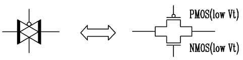
일반적으로 낮은 문턱 전압을 가지는 트랜지스터와 높은 문턱 전압을 가지는 트랜지스터의 구분에 있어서, 1.2V 동작하는 130nm 규격의 트랜지스터의 경우 낮은 문턱 전압은 0.24V 정도, 높은 문턱 전압은 0.44V 정도이다.In general, in the classification of a transistor having a low threshold voltage and a transistor having a high threshold voltage, a 130 nm standard transistor operating at 1.2 V has a low threshold voltage of about 0.24 V and a high threshold voltage of about 0.44 V.
도 4는 본 발명에 따른 MTCMOS 래치회로를 나타난 도면, 도 5는 본 발명에 따른 슬립 신호 발생 회로를 나타낸 도면, 도 6은 본 발명에 따른 클럭 신호 발생 회로를 나타낸 도면, 도 7a 내지 도 7e는 도 4에 도시된 MTCMOS 래치회로내의 개별 회로도를 나타낸 도면이다.4 is a view showing an MTCMOS latch circuit according to the present invention, FIG. 5 is a view showing a sleep signal generating circuit according to the present invention, FIG. 6 is a view showing a clock signal generating circuit according to the present invention, and FIGS. 7A to 7E 4 is a diagram showing an individual circuit diagram in the MTCMOS latch circuit shown in FIG.
도 4를 참조하면, MTCMOS 래치회로는 슬립 신호(SP)와 반전 슬립 신호(SPb)의 제어하에 입력 데이터(D)를 반전시켜 출력하는 데이터 반전 회로부(400), 상기 데이터 반전 회로부(400)에서 출력되는 데이터 신호를 클럭 제어 신호(CLK)의 제어에 의해 전달하는 전달 게이트(410), 상기 전달 게이트(410)에서 출력되는 데이터 신호를 RS신호(리셋 제어 신호)와 슬립 제어 신호(SLP)의 제어에 의해 출력하는 신호 제어 회로부(420), 상기 신호 제어 회로부에서 출력되는 신호를 피드백하여 슬립 모드시 데이터를 보전하는 피드백 회로부(430)를 포함한다. Referring to FIG. 4, the MTCMOS latch circuit includes a data
상기 반전 회로부(400)는 입력 데이터(D)를 수신하여 반전시키는 제1 인버터(402), 전원전압에 연결된 소스와 슬립신호(SP)를 수신하는 게이트와 상기 제1 인버터(402)에 연결된 드레인을 갖는 제1 PMOS 트랜지스터(G1), 상기 제1 인버터(402)에 연결된 드레인과 반전 슬립 신호(SPb)를 수신하는 게이트와 접지에 연결된 소스를 갖는 제1 NMOS 트랜지스터(G2)를 포함한다. The inverting
여기서, 상기 제1 인버터(402)는 데이터를 최단 경로로 전달하기 위해서 낮은 문턱 전압을 가진 PMOS 트랜지스터와 NMOS 트랜지스터를 사용하여 구성된 것이다.In this case, the
상기 반전 회로부(400)는 도 7a와 같은 등가 회로로 표현된다.The inverting
도 7a를 참조하면, 상기 제1 PMOS 트랜지스터(G1)과 제1 NMOS 트랜지스터(G2)는 높은 문턱 전압을 갖고, 상기 제1 인버터(402)는 각각 낮은 문턱 전압을 가진 PMOS 트랜지스터와 NMOS 트랜지스터로 구성됨을 알 수 있다.Referring to FIG. 7A, the first PMOS transistor G1 and the first NMOS transistor G2 have a high threshold voltage, and the
상기 전달 게이트(410)는 클럭신호(CP)와 반전 클럭신호(CPb)의 제어하에 상기 데이터 반전 회로부(400)에서 출력되는 데이터 신호를 상기 신호 제어 회로부(420)에 전달하는 것으로서, 도 7b와 같이 각각 낮은 문턱 전압을 가진 PMOS 트랜지스터와 NMOS 트랜지스터에 의해 구성된다. The
상기 신호 제어 회로부(420)는 RS 신호, 슬립신호(SP)와 반전 슬립신호(SPb) 의 제어하에 상기 전달 게이트(410)의 출력신호를 수신하여 출력하는 NOR 게이트(422), 전원전압에 연결된 소스와 슬립신호(SP)를 수신하는 게이트와 상기 NOR 게이트(422)에 연결된 드레인을 갖는 제2 PMOS 트랜지스터(G3), 상기 NOR 게이트(422)에 연결된 드레인과 반전 슬립신호(SPb)를 수신하는 게이트와 접지에 연결된 소스를 갖는 제2 NMOS 트랜지스터(G4)를 포함한다.The
상기 신호 제어 회로부(420)는 도 7c와 같은 등가 회로를 갖는 것으로서, 상기 제2 PMOS 트랜지스터(G3)와 상기 제2 NMOS 트랜지스터(G4)는 높은 문턱 전압을 갖고, 상기 NOR 게이트(422)는 각각 낮은 문턱 전압을 갖는 PMOS 트랜지스터와 NMOS 트랜지스터에 의해 구성된다.The
상기 피드백 회로부(430)는 MTCMOS 래치회로가 슬립 모드로 동작시 데이터를 유지하게 하는 것으로서, 누설 전류가 적은 높은 문턱 전압을 갖는 PMOS 트랜지스터와 NMOS 트랜지스터에 의해 구성된다. The
즉, 상기 피드백 회로부(430)는 상기 신호 제어 회로부(420)에서 출력되는 신호(Q)를 반전시켜 출력하는 제2 인버터(432), 상기 신호 제어 회로부(420)에서 출력되는 신호(Q)를 수신하는 소스와 상기 제2 인버터(432)에서 출력되는 신호를 수신하는 게이트와 출력(Q)과 연결된 드레인을 갖는 제3 PMOS 트랜지스터(G5), 상기 신호 제어 회로부(420)의 NOR 게이트(422)에 연결되는 드레인과 상기 제2 인버터(432)에서 출력되는 신호를 수신하는 게이트, 접지에 연결된 소스를 갖는 제3 NMOS 트랜지스터(G6), 클럭 신호(CP)와 반전 클럭신호(CPb)의 제어에 의해 상기 제2 인버터(432)의 출력신호를 수신하여 상기 신호 제어 회로부(420)에 전달하는 피 드백 전달 게이트(434)를 포함한다. That is, the
상기 제2 인버터(432)는 도 7d와 같이 각각 높은 문턱 전압을 갖는 PMOS 트랜지스터와 NMOS 트랜지스터에 의해 구성되고, 상기 피드백 전달 게이트(434)는 도 7e와 같이 각각 높은 문턱 전압을 갖는 PMOS 트랜지스터와 NMOS 트랜지스터에 의해 구성된다.The
이하 상기와 같이 구성된 MTCMOS 래치회로의 동작에 대하여 설명하기로 한다.Hereinafter, the operation of the MTCMOS latch circuit configured as described above will be described.
상기 MTCMOS 래치회로는 RS 신호가 high 상태이면, 데이터(D) 및 슬립제어신호(SLP)의 입력상태에 상관없이 출력 Q는 low 상태로 된다.In the MTCMOS latch circuit, when the RS signal is high, the output Q is turned low regardless of the input state of the data D and the sleep control signal SLP.
상기 RS 신호가 low 상태이면, MTCMOS 래치회로는 슬립 제어신호(SLP)에 따라 액티브 모드 또는 슬립 모드로 동작을 하게 된다. When the RS signal is low, the MTCMOS latch circuit operates in the active mode or the sleep mode according to the sleep control signal SLP.
즉, 상기 RS 신호가 low 상태이고, 슬립 제어신호(SLP)가 low 상태이면, 상기 MTCMOS 래치회로는 액티브 모드로 동작하고, 상기 슬립 제어 신호(SLP)가 high 상태이면, 상기 MTCMOS 래치회로는 슬립모드로 동작한다.That is, when the RS signal is low and the sleep control signal SLP is low, the MTCMOS latch circuit operates in an active mode, and when the sleep control signal SLP is high, the MTCMOS latch circuit sleeps. Operate in mode.
먼저, 상기 MTCMOS 래치회로가 액티브 모드로 동작할 때의 회로 동작에 대해 설명하기로 한다. First, the circuit operation when the MTCMOS latch circuit operates in the active mode will be described.
상기 RS 신호가 low 상태이고, 슬립 제어신호(SLP)가 low 상태이면, 높은 문턱 전압을 갖는 제1 및 제2 PMOS 트랜지스터(G1, G3)와 제1 및 제2 NMOS 트랜지스터(G2, G4)는 모두 on 상태가 된다. When the RS signal is low and the sleep control signal SLP is low, the first and second PMOS transistors G1 and G3 and the first and second NMOS transistors G2 and G4 having a high threshold voltage are All are on.
즉, 상기 슬립 제어 신호(SLP)가 low이면, 도 5와 같은 슬립 신호 발생 회로에 의해 low 상태의 슬립 신호(SP)와 high 상태의 반전 슬립신호(SPb)가 생성된다.That is, when the sleep control signal SLP is low, the sleep signal generation circuit shown in FIG. 5 generates the low sleep signal SP and the high inversion sleep signal SPb.
그러면, 상기 높은 문턱전압을 갖는 제1 및 제2 PMOS 트랜지스터(G1, G3)와 제1 및 제2 NMOS 트랜지스터(G2, G4)는 상기 low 상태의 슬립 신호(SP)와 high 상태의 반전 슬립신호(SPb)에 의해 on 상태가 된다. Then, the first and second PMOS transistors G1 and G3 and the first and second NMOS transistors G2 and G4 having the high threshold voltage are in the low state sleep signal SP and the high state inverted sleep signal. It is turned on by (SPb).
상기와 같은 상태에서 클럭 제어신호(CLK)가 high 상태이면, 도 6과 같은 클럭 신호 발생 회로에 의해 클럭신호(CP)는 low상태이고, 반전 클럭신호(CPb)는 high상태가 되어, 상기 전달 게이트(410)는 on 상태가 되고, 상기 피드백 전달 게이트(434)는 off 상태가 된다. When the clock control signal CLK is high in the above state, the clock signal CP is in the low state and the inverted clock signal CPb is in the high state by the clock signal generation circuit as shown in FIG.
따라서, 입력데이터(D)는 상기 데이터 반전회로부(400), 상기 전달게이트(410) 및 상기 신호 제어 회로부(420)를 통해 출력된다.Therefore, the input data D is output through the data
만약, 상기와 같이 상기 RS 신호가 low 상태이고, 슬립 제어신호(SLP)가 low 상태일 때, 상기 클럭제어신호(CLK)가 low 상태이면, 클럭신호(CP)는 low상태이고, 반전 클럭신호(CPb)는 high 상태가 되어, 상기 전달게이트(410)는 off 상태가 되고, 상기 피드백 전달게이트(434)는 on상태가 되어 이전의 데이터(D)가 출력(Q)된다. If the RS signal is low and the sleep control signal SLP is low as described above, if the clock control signal CLK is low, the clock signal CP is low and the inverted clock signal is CPb is in a high state, the
상기와 같이 MTCMOS 래치회로가 액티브 모드로 동작할 때, 상기 MTCMOS 래치회로는 클럭제어신호(CLK)의 high/low 상태가 지속됨에 따라 데이터(D)를 계속 출력한다.As described above, when the MTCMOS latch circuit operates in the active mode, the MTCMOS latch circuit continuously outputs data D as the high / low state of the clock control signal CLK continues.
상기와 같이 상기 MTCMOS 래치회로가 액티브 모드에서 동작을 할 때에는 데 이터 반전회로부(400)내의 제1 인버터(402), 전달게이트(410) 및 신호 제어 회로부(420)내의 NOR 게이트(422)는 모두 낮은 문턱전압을 갖는 PMOS 트랜지스터 및 NMOS 트랜지스터로 구성되어 있기 때문에 데이터 전송시 동작속도가 매우 빠르다. As described above, when the MTCMOS latch circuit operates in the active mode, the
상기 슬립 신호 발생 회로에 대하여 도 5를 참조하면, 상기 슬립 신호 발생 회로는 슬립 제어 신호(SLP)를 반전시켜 반전 슬립 신호(SPb)를 출력하는 제3 인버터(500), 상기 제3 인버터(500)에서 출력되는 신호를 반전시켜 슬립 신호(SP)를 출력하는 제4 인버터(510)로 구성된다. Referring to FIG. 5 with respect to the sleep signal generation circuit, the sleep signal generation circuit inverts the sleep control signal SLP to output an inverted sleep signal SPb, and the
따라서, 상기 슬립 신호 발생 회로는 low 상태의 슬립 제어 신호(SLP)가 입력되면, low 상태의 슬립 신호(SP)와 high 상태의 반전 슬립신호(SPb)를 출력하고, high 상태의 슬립 제어 신호(SLP)가 입력되면, high 상태의 슬립 신호(SP)와 low 상태의 반전 슬립신호(SPb)를 출력한다. Therefore, when the sleep control signal SLP in the low state is input, the sleep signal generating circuit outputs the low sleep signal SP and the high inversion sleep signal SPb, and the high sleep control signal ( When the SLP is input, the high state sleep signal SP and the low state inversion sleep signal SPb are output.
상기 클럭 신호 발생 회로에 대하여 도 6을 참조하면, 상기 클럭 신호 발생 회로는 클럭 제어 신호(CLK)를 반전시켜 반전 클럭 신호(CPb)를 출력하는 제5 인버터(600), 상기 제5 인버터(600)에서 출력되는 신호를 반전시켜 클럭 신호(CP)를 출력하는 제6 인버터(610)로 구성된다. Referring to FIG. 6 with respect to the clock signal generation circuit, the clock signal generation circuit inverts the clock control signal CLK and outputs the inverted clock signal CPb and the
따라서, 상기 클럭 신호 발생 회로는 low 상태의 클럭 제어 신호(CLK)가 입력되면, low 상태의 클럭 신호(CP)와 high 상태의 반전 클럭신호(CPb)를 출력하고, high 상태의 클럭 입력 신호(CLK)가 입력되면, high 상태의 클럭 신호(CP)와 low 상태의 반전 클럭 신호(CPb)를 출력한다. Therefore, when the clock control signal CLK in the low state is input, the clock signal generation circuit outputs the clock signal CP in the low state and the inverted clock signal CPb in the high state, and the clock input signal in the high state ( When CLK) is input, the clock signal CP in the high state and the inverted clock signal CPb in the low state are output.
다음으로, 상기 MTCMOS 래치회로가 슬립 모드로 동작할 때의 회로 동작에 대해 설명하기로 한다. Next, a circuit operation when the MTCMOS latch circuit operates in the sleep mode will be described.
상기 RS 신호가 low 상태이고, 상기 슬립 제어 신호(SLP)가 high 상태일 때, MTCMOS 래치회로는 슬립모드로 동작한다.When the RS signal is low and the sleep control signal SLP is high, the MTCMOS latch circuit operates in a sleep mode.
따라서, 상기 RS 신호가 low 상태이고, 슬립 제어신호(SLP)가 high 상태(즉, 슬립 신호(SP)가 high 상태이고, 반전 슬립신호(SPb)가 low 상태)이면, 높은 문턱전압을 갖는 제1 및 제2 PMOS 트랜지스터(G1, G3)와 제1 및 제2 NMOS 트랜지스터(G2, G4)는 모두 off 상태가 되어, 출력 Q의 데이터 상태는 상기 피드백 회로부(430)에 보전된다.Therefore, when the RS signal is low, and the sleep control signal SLP is high (that is, the sleep signal SP is high and the inverted sleep signal SPb is low), The first and second PMOS transistors G1 and G3 and the first and second NMOS transistors G2 and G4 are both turned off, and the data state of the output Q is held in the
즉, 출력 Q가 low 상태인 경우, 상기 제2 인버터(432)에 의해 상기 제3 NMOS 트랜지스터(G6)의 게이트에는 high가 인가되어 턴온되고, 상기 제3 PMOS 트랜지스터(G5)의 게이트에는 high가 인가되어 턴오프된다. That is, when the output Q is low, high is applied to the gate of the third NMOS transistor G6 by the
이때, 클럭제어신호가 low이면, 상기 피드백 전달 게이트(434)는 on상태가 되어, 상기 NOR 게이트(422)에는 high가 인가되어 출력 Q는 low가 된다. 이때 출력 Q는 도 7c의 NOR 게이트 회로에서 보는 바와 같이 NOR 게이트(422) 내부의 NMOS 트랜지스터와 상기 제3 NMOS 트랜지스터(G6)를 거쳐 접지(ground)와 연결되어 출력 Q의 low 상태를 유지하게 된다. At this time, when the clock control signal is low, the
또한, 출력 Q가 high 상태인 경우, 상기 제2 인버터(432)에 의해 상기 제3 NMOS 트랜지스터(G6)의 게이트에는 low가 인가되어 턴 오프되므로, 상기 NOR 게이트(422)는 동작하지 않게 된다. 그리고, 상기 PMOS 트랜지스터(G5)의 게이트에는 상기 제2 인버터(432)에 의해 low가 인가되어 턴 온되고, 상기 제3 PMOS 트랜지스터(G5)의 소스 및 드레인에는 high로 인해 결과적으로 출력 Q는 high를 유지하게 된다. In addition, when the output Q is in a high state, since the low is applied to the gate of the third NMOS transistor G6 by the
상기와 같이 상기 피드백 회로부(430)는 단지 데이터를 유지하는 것이 주목적이므로 누설전류가 적은 높은 문턱전압을 갖는 PMOS 트랜지스터 및 NMOS 트랜지스터로 회로가 구성되며, 가능한 최소 크기로 설계될 수 있다. As described above, since the
다음으로, MTCMOS 래치회로가 슬립모드에서 액티브모드로 전환할 경우, 즉 슬립 모드에서 슬립 제어 신호(SLP)를 low 상태로 하면, 상기 MTCMOS 래치회로는 액티브 모드로 동작을 한다.Next, when the MTCMOS latch circuit switches from the sleep mode to the active mode, that is, when the sleep control signal SLP is turned low in the sleep mode, the MTCMOS latch circuit operates in the active mode.
즉, 상기 MTCMOS 래치회로는 슬립 제어신호(SLP)가 low 상태(즉, 슬립 신호(SP)가 low 상태이고, 반전 슬립신호(SPb)가 high 상태)이면, 높은 문턱전압을 갖는 제1 및 제2 PMOS 트랜지스터(G1, G3)와 제1 및 제2 NMOS 트랜지스터(G2, G4)는 모두 on 상태가 된다. That is, in the MTCMOS latch circuit, when the sleep control signal SLP is in a low state (that is, the sleep signal SP is in a low state and the inversion sleep signal SPb is in a high state), the MTCMOS latch circuit has a first threshold and a first threshold voltage having a high threshold voltage. Both PMOS transistors G1 and G3 and the first and second NMOS transistors G2 and G4 are turned on.
상기와 같은 상태에서 클럭 제어신호(CLK)가 high 상태이면, 클럭신호(CP)는 high상태이고, 반전 클럭신호(CPb)는 low상태가 되어, 상기 전달 게이트(410)는 on 상태가 되고, 상기 피드백 전달 게이트(434)는 off 상태가 된다. In the above state, when the clock control signal CLK is in the high state, the clock signal CP is in the high state, the inverted clock signal CPb is in the low state, and the
따라서, 입력데이터(D)는 상기 데이터 반전회로부(400), 상기 전달게이트(410) 및 상기 신호 제어 회로부(420)를 통해 출력된다.Therefore, the input data D is output through the data
또한, 상기 클럭제어신호(CLK)가 low 상태이면, 클럭신호(CP)는 low상태이 고, 반전 클럭신호(CPb)는 high 상태가 되어, 상기 전달게이트(410)는 off 상태가 되고, 상기 피드백 전달게이트(434)는 on상태가 되어 이전의 데이터(D)가 출력(Q)된다. In addition, when the clock control signal CLK is in a low state, the clock signal CP is in a low state, the inverted clock signal CPb is in a high state, and the
도 8은 본 발명에 따른 MTCMOS 래치회로의 신호 동작 타이밍도이다. 8 is a signal operation timing diagram of the MTCMOS latch circuit according to the present invention.
도 8을 참조하면, 리셋제어신호(RS)가 low, 클럭신호(CLK)가 high, 데이터신호(D)가 high인 경우, 슬립모드에서 보전된 출력 Q의 high 는 슬립모드에서 액티브모드로 전환할 때에 클럭 제어 신호(CLK)와 데이터 신호가 모두 high인 경우 출력 Q의 high 상태를 그대로 유지하게 된다. Referring to FIG. 8, when the reset control signal RS is low, the clock signal CLK is high, and the data signal D is high, the high value of the output Q held in the sleep mode is switched from the sleep mode to the active mode. When the clock control signal CLK and the data signal are both high, the output Q remains high.
슬립모드에서의 출력 Q의 A-영역의 가장자리는 출력 Q의 high 상태가 슬립모드 전후 동일하게 유지됨을 알 수 있다. The edge of the A-area of the output Q in the sleep mode can be seen that the high state of the output Q remains the same before and after the sleep mode.
도 9는 본 발명의 다른 실시예에 따른 MTCMOS 래치 회로를 나타낸 도면이다. 9 illustrates an MTCMOS latch circuit according to another embodiment of the present invention.
도 9를 참조하면, MTCMOS 래치회로는 데이터 반전 회로부(900), 전달 게이트(910), 신호 제어 회로부(920), 피드백 회로부(930)를 포함한다.9, the MTCMOS latch circuit includes a data
상기 데이터 반전 회로부(900), 전달 게이트(910), 신호 제어 회로부(920)는 도 4와 같으므로 그 설명은 생략하기로 한다.Since the data
상기 피드백 회로부(930)는 도 4와 비교할 때, 피드백 전달게이트 없이 가상접지(virtual ground)(도 7c의 x 노드)를 이용하여 출력 Q의 low를 보전한다. Compared to FIG. 4, the
즉, MTCMOS 래치회로가 슬립모드시에, 출력 Q가 low 인 경우, 제3 NMOS 트랜지스터(G6)의 게이트는 high가 인가되어 턴 온상태가 되며, 제3 NMOS 트랜지스터(G6)의 드레인에 가상접지(virtual ground)(도 7c의 x노드)가 형성되어 결과적 으로 출력 Q는 low가 유지된다. That is, when the output Q is low when the MTCMOS latch circuit is in the sleep mode, the gate of the third NMOS transistor G6 is turned on by applying high to the drain of the third NMOS transistor G6. (virtual ground) (x node in Figure 7c) is formed, resulting in the output Q remains low.
그리고 출력 Q가 high 인 경우, 도 4와 마찬가지로, 제3 PMOS 트랜지스터(G5)의 게이트는 low가 되며, 상기 제3 PMOS 트랜지스터(G5)의 소스 및 드레인에는 high로 인해 결과적으로 출력 Q의 high 가 유지된다. When the output Q is high, as in FIG. 4, the gate of the third PMOS transistor G5 becomes low, and the high of the source Q and drain of the third PMOS transistor G5 results in high output Q. maintain.
본 발명은 상기 실시예에 한정되지 않으며, 많은 변형이 본 발명의 사상 내에서 당 분야에서 통상의 지식을 가진 자에 의하여 가능함은 물론이다.The present invention is not limited to the above embodiments, and many variations are possible by those skilled in the art within the spirit of the present invention.
상술한 바와 같이 본 발명에 따르면, 소자의 기술이 나노급으로 스케링됨에 따라 누설전류에 의한 전력소모를 최소화시킬 뿐만 아니라 낮은 문턱 전압을 갖는 소자의 사용으로 인해 로직 회로의 고속동작에도 크게 기여할 수 있는 MTCMOS 래치회로를 제공할 수 있다. As described above, according to the present invention, as the technology of the device is nanoscaled, the power consumption due to leakage current is not only minimized, but also due to the use of a device having a low threshold voltage, it can greatly contribute to the high speed operation of the logic circuit. An MTCMOS latch circuit can be provided.
또한, 본 발명에 따르면, MTCMOS 기술을 이용한 고속, 저전력 래치회로는 동기식 순차 시스템으로서 작동하는 고성능의 마이크로 프로세서등에 널리 활용될 수 있는 MTCMOS 래치회로를 제공할 수 있다. In addition, according to the present invention, the high-speed, low-power latch circuit using the MTCMOS technology can provide an MTCMOS latch circuit that can be widely used in a high-performance microprocessor or the like operating as a synchronous sequential system.
Claims (13)
Priority Applications (1)
| Application Number | Priority Date | Filing Date | Title |
|---|---|---|---|
| US11/607,743 US7391249B2 (en) | 2005-12-07 | 2006-12-01 | Multi-threshold CMOS latch circuit |
Applications Claiming Priority (2)
| Application Number | Priority Date | Filing Date | Title |
|---|---|---|---|
| KR1020050119077 | 2005-12-07 | ||
| KR20050119077 | 2005-12-07 |
Publications (1)
| Publication Number | Publication Date |
|---|---|
| KR100702364B1 true KR100702364B1 (en) | 2007-04-02 |
Family
ID=38160601
Family Applications (1)
| Application Number | Title | Priority Date | Filing Date |
|---|---|---|---|
| KR1020060060355A Expired - Fee Related KR100702364B1 (en) | 2005-12-07 | 2006-06-30 | MTC MOS Latch Circuit |
Country Status (1)
| Country | Link |
|---|---|
| KR (1) | KR100702364B1 (en) |
Cited By (2)
| Publication number | Priority date | Publication date | Assignee | Title |
|---|---|---|---|---|
| WO2010090980A3 (en) * | 2009-02-04 | 2010-12-09 | Fairchild Semiconductor Corporation | High speed, low power consumption, isolated analog cmos unit |
| KR20230148015A (en) | 2022-04-15 | 2023-10-24 | 주식회사 티앤알바이오팹 | Scaffold for breast reconstruction |
Citations (6)
| Publication number | Priority date | Publication date | Assignee | Title |
|---|---|---|---|---|
| JPH1197984A (en) | 1997-09-19 | 1999-04-09 | Nippon Telegr & Teleph Corp <Ntt> | Latch circuit |
| US6538471B1 (en) | 2001-10-10 | 2003-03-25 | International Business Machines Corporation | Multi-threshold flip-flop circuit having an outside feedback |
| US6794914B2 (en) | 2002-05-24 | 2004-09-21 | Qualcomm Incorporated | Non-volatile multi-threshold CMOS latch with leakage control |
| KR20050104530A (en) * | 2004-04-29 | 2005-11-03 | 삼성전자주식회사 | Mtcmos flip-flop, mtcmos circuit including the same, and method for generating the same |
| US6989702B2 (en) | 2002-07-11 | 2006-01-24 | Texas Instruments Incorporated | Retention register with normal functionality independent of retention power supply |
| US7046063B2 (en) | 2004-04-08 | 2006-05-16 | International Business Machines Corporation | Interface circuit for coupling between logic circuit domains |
-
2006
- 2006-06-30 KR KR1020060060355A patent/KR100702364B1/en not_active Expired - Fee Related
Patent Citations (6)
| Publication number | Priority date | Publication date | Assignee | Title |
|---|---|---|---|---|
| JPH1197984A (en) | 1997-09-19 | 1999-04-09 | Nippon Telegr & Teleph Corp <Ntt> | Latch circuit |
| US6538471B1 (en) | 2001-10-10 | 2003-03-25 | International Business Machines Corporation | Multi-threshold flip-flop circuit having an outside feedback |
| US6794914B2 (en) | 2002-05-24 | 2004-09-21 | Qualcomm Incorporated | Non-volatile multi-threshold CMOS latch with leakage control |
| US6989702B2 (en) | 2002-07-11 | 2006-01-24 | Texas Instruments Incorporated | Retention register with normal functionality independent of retention power supply |
| US7046063B2 (en) | 2004-04-08 | 2006-05-16 | International Business Machines Corporation | Interface circuit for coupling between logic circuit domains |
| KR20050104530A (en) * | 2004-04-29 | 2005-11-03 | 삼성전자주식회사 | Mtcmos flip-flop, mtcmos circuit including the same, and method for generating the same |
Cited By (3)
| Publication number | Priority date | Publication date | Assignee | Title |
|---|---|---|---|---|
| WO2010090980A3 (en) * | 2009-02-04 | 2010-12-09 | Fairchild Semiconductor Corporation | High speed, low power consumption, isolated analog cmos unit |
| US8269279B2 (en) | 2009-02-04 | 2012-09-18 | Fairchild Semiconductor Corporation | High speed, low power consumption, isolated analog CMOS unit |
| KR20230148015A (en) | 2022-04-15 | 2023-10-24 | 주식회사 티앤알바이오팹 | Scaffold for breast reconstruction |
Similar Documents
| Publication | Publication Date | Title |
|---|---|---|
| US7576582B2 (en) | Low-power clock gating circuit | |
| JP4262053B2 (en) | MTCMOS flip-flop circuit that can store data in sleep mode | |
| JP3080062B2 (en) | Semiconductor integrated circuit | |
| TWI520489B (en) | Low leakage and data retention circuit | |
| JP5671577B2 (en) | Integrated circuit having low leakage data holding circuit and method thereof | |
| CN106664078B (en) | Multi-threshold CMOS sequential circuit based on low leakage shadow latch | |
| KR20090027042A (en) | MTCMOOS Flip-Flops with Retention | |
| US7391249B2 (en) | Multi-threshold CMOS latch circuit | |
| CN107408939A (en) | Electronic circuit | |
| US20110018584A1 (en) | Semiconductor integrated circuit | |
| JP4122954B2 (en) | Semiconductor integrated circuit | |
| CN109217860B (en) | Semiconductor device with power gating scheme | |
| US10530365B1 (en) | Low voltage level shifter suitable for use with subthreshold logic | |
| JPH0865149A (en) | Ouasi-static no-loss gate | |
| JP3511355B2 (en) | Output circuit | |
| KR100702364B1 (en) | MTC MOS Latch Circuit | |
| KR102024470B1 (en) | Low Power Flip-Flop | |
| US7420403B2 (en) | Latch circuit and flip-flop | |
| KR100921509B1 (en) | Low power clock gating circuit | |
| KR100850177B1 (en) | MTCMOS Flip-Flop Circuit | |
| KR101004670B1 (en) | Power gating circuit and semiconductor device comprising same | |
| JP3500598B2 (en) | Latch circuit | |
| TWI583137B (en) | Synchroniser flip-flop | |
| KR100703720B1 (en) | Semiconductor integrated circuit device with power gating circuit | |
| CN110557102B (en) | Semiconductor device |
Legal Events
| Date | Code | Title | Description |
|---|---|---|---|
| A201 | Request for examination | ||
| PA0109 | Patent application |
St.27 status event code: A-0-1-A10-A12-nap-PA0109 |
|
| PA0201 | Request for examination |
St.27 status event code: A-1-2-D10-D11-exm-PA0201 |
|
| D13-X000 | Search requested |
St.27 status event code: A-1-2-D10-D13-srh-X000 |
|
| D14-X000 | Search report completed |
St.27 status event code: A-1-2-D10-D14-srh-X000 |
|
| E701 | Decision to grant or registration of patent right | ||
| PE0701 | Decision of registration |
St.27 status event code: A-1-2-D10-D22-exm-PE0701 |
|
| GRNT | Written decision to grant | ||
| PR0701 | Registration of establishment |
St.27 status event code: A-2-4-F10-F11-exm-PR0701 |
|
| PR1002 | Payment of registration fee |
St.27 status event code: A-2-2-U10-U11-oth-PR1002 Fee payment year number: 1 |
|
| PG1601 | Publication of registration |
St.27 status event code: A-4-4-Q10-Q13-nap-PG1601 |
|
| PN2301 | Change of applicant |
St.27 status event code: A-5-5-R10-R13-asn-PN2301 St.27 status event code: A-5-5-R10-R11-asn-PN2301 |
|
| PR1001 | Payment of annual fee |
St.27 status event code: A-4-4-U10-U11-oth-PR1001 Fee payment year number: 4 |
|
| PR1001 | Payment of annual fee |
St.27 status event code: A-4-4-U10-U11-oth-PR1001 Fee payment year number: 5 |
|
| PR1001 | Payment of annual fee |
St.27 status event code: A-4-4-U10-U11-oth-PR1001 Fee payment year number: 6 |
|
| L13-X000 | Limitation or reissue of ip right requested |
St.27 status event code: A-2-3-L10-L13-lim-X000 |
|
| U15-X000 | Partial renewal or maintenance fee paid modifying the ip right scope |
St.27 status event code: A-4-4-U10-U15-oth-X000 |
|
| FPAY | Annual fee payment |
Payment date: 20130304 Year of fee payment: 7 |
|
| PR1001 | Payment of annual fee |
St.27 status event code: A-4-4-U10-U11-oth-PR1001 Fee payment year number: 7 |
|
| FPAY | Annual fee payment |
Payment date: 20140303 Year of fee payment: 8 |
|
| PR1001 | Payment of annual fee |
St.27 status event code: A-4-4-U10-U11-oth-PR1001 Fee payment year number: 8 |
|
| PN2301 | Change of applicant |
St.27 status event code: A-5-5-R10-R13-asn-PN2301 St.27 status event code: A-5-5-R10-R11-asn-PN2301 |
|
| FPAY | Annual fee payment |
Payment date: 20150226 Year of fee payment: 9 |
|
| PR1001 | Payment of annual fee |
St.27 status event code: A-4-4-U10-U11-oth-PR1001 Fee payment year number: 9 |
|
| LAPS | Lapse due to unpaid annual fee | ||
| PC1903 | Unpaid annual fee |
St.27 status event code: A-4-4-U10-U13-oth-PC1903 Not in force date: 20160328 Payment event data comment text: Termination Category : DEFAULT_OF_REGISTRATION_FEE |
|
| P22-X000 | Classification modified |
St.27 status event code: A-4-4-P10-P22-nap-X000 |
|
| PC1903 | Unpaid annual fee |
St.27 status event code: N-4-6-H10-H13-oth-PC1903 Ip right cessation event data comment text: Termination Category : DEFAULT_OF_REGISTRATION_FEE Not in force date: 20160328 |