KR100675009B1 - Data Delay Control Circuits and Methods - Google Patents
Data Delay Control Circuits and Methods Download PDFInfo
- Publication number
- KR100675009B1 KR100675009B1 KR1020060009805A KR20060009805A KR100675009B1 KR 100675009 B1 KR100675009 B1 KR 100675009B1 KR 1020060009805 A KR1020060009805 A KR 1020060009805A KR 20060009805 A KR20060009805 A KR 20060009805A KR 100675009 B1 KR100675009 B1 KR 100675009B1
- Authority
- KR
- South Korea
- Prior art keywords
- delay
- clock
- change
- signal
- data
- Prior art date
- Legal status (The legal status is an assumption and is not a legal conclusion. Google has not performed a legal analysis and makes no representation as to the accuracy of the status listed.)
- Expired - Fee Related
Links
Images


Classifications
-
- H—ELECTRICITY
- H03—ELECTRONIC CIRCUITRY
- H03L—AUTOMATIC CONTROL, STARTING, SYNCHRONISATION OR STABILISATION OF GENERATORS OF ELECTRONIC OSCILLATIONS OR PULSES
- H03L7/00—Automatic control of frequency or phase; Synchronisation
-
- H—ELECTRICITY
- H03—ELECTRONIC CIRCUITRY
- H03K—PULSE TECHNIQUE
- H03K5/00—Manipulating of pulses not covered by one of the other main groups of this subclass
- H03K5/01—Shaping pulses
- H03K5/04—Shaping pulses by increasing duration; by decreasing duration
- H03K5/06—Shaping pulses by increasing duration; by decreasing duration by the use of delay lines or other analogue delay elements
-
- H—ELECTRICITY
- H03—ELECTRONIC CIRCUITRY
- H03K—PULSE TECHNIQUE
- H03K3/00—Circuits for generating electric pulses; Monostable, bistable or multistable circuits
- H03K3/02—Generators characterised by the type of circuit or by the means used for producing pulses
- H03K3/027—Generators characterised by the type of circuit or by the means used for producing pulses by the use of logic circuits, with internal or external positive feedback
- H03K3/03—Astable circuits
- H03K3/0315—Ring oscillators
-
- H—ELECTRICITY
- H03—ELECTRONIC CIRCUITRY
- H03K—PULSE TECHNIQUE
- H03K5/00—Manipulating of pulses not covered by one of the other main groups of this subclass
- H03K5/13—Arrangements having a single output and transforming input signals into pulses delivered at desired time intervals
-
- H—ELECTRICITY
- H03—ELECTRONIC CIRCUITRY
- H03L—AUTOMATIC CONTROL, STARTING, SYNCHRONISATION OR STABILISATION OF GENERATORS OF ELECTRONIC OSCILLATIONS OR PULSES
- H03L7/00—Automatic control of frequency or phase; Synchronisation
- H03L7/06—Automatic control of frequency or phase; Synchronisation using a reference signal applied to a frequency- or phase-locked loop
- H03L7/08—Details of the phase-locked loop
- H03L7/0805—Details of the phase-locked loop the loop being adapted to provide an additional control signal for use outside the loop
-
- H—ELECTRICITY
- H03—ELECTRONIC CIRCUITRY
- H03K—PULSE TECHNIQUE
- H03K5/00—Manipulating of pulses not covered by one of the other main groups of this subclass
- H03K2005/00013—Delay, i.e. output pulse is delayed after input pulse and pulse length of output pulse is dependent on pulse length of input pulse
- H03K2005/00019—Variable delay
- H03K2005/00058—Variable delay controlled by a digital setting
-
- H—ELECTRICITY
- H03—ELECTRONIC CIRCUITRY
- H03K—PULSE TECHNIQUE
- H03K5/00—Manipulating of pulses not covered by one of the other main groups of this subclass
- H03K2005/00013—Delay, i.e. output pulse is delayed after input pulse and pulse length of output pulse is dependent on pulse length of input pulse
- H03K2005/00078—Fixed delay
- H03K2005/00143—Avoiding variations of delay due to temperature
Landscapes
- Physics & Mathematics (AREA)
- Nonlinear Science (AREA)
- Pulse Circuits (AREA)
Abstract
본 발명은 반도체 칩의 설계시 특정크기의 예상지연(expected delay)을 삽입해야 하는 경우에 동작 온도, 동작 전압 및 제조공정 등과 같은 칩의 동작 환경 변화가 발생하더라도, 이를 데이터 지연에 적응적으로 적용하기 위한 데이터 지연 조절 회로 및 그 방법을 제공하기 위한 것이다. 이를 위해 본 발명은, 지연셀(delay cell)의 지연 크기 변화를 대변할 수 있는 클럭 발진기를 구비하여 자동으로 지연 크기를 조절할 수 있도록 한다. 이렇듯, 본 발명은 반도체 장치의 동작환경이 변화하더라도 모니터링 회로와 다수의 지연 패스(delay path)를 구비하여 예상 지연값을 갖는 지연 패스를 제공하여 데이터 신호의 지연크기를 조정할 수 있도록 함으로써, 변화된 환경에 적응하여 데이터 지연신호를 자동으로 생성할 수 있도록 하는 효과가 있다.The present invention adaptively applies to data delay even if a change in operating environment of the chip such as operating temperature, operating voltage, and manufacturing process occurs when a certain size of expected delay must be inserted in the design of a semiconductor chip. To provide a data delay control circuit and a method thereof. To this end, the present invention is equipped with a clock oscillator that can represent the change in the delay size of the delay cell (delay cell) to automatically adjust the delay size. As described above, the present invention provides a delayed path having an expected delay value by providing a monitoring circuit and a plurality of delay paths even when the operating environment of the semiconductor device changes, thereby allowing the delay size of the data signal to be adjusted. It is effective to automatically generate the data delay signal by adapting to.
Description
본 발명의 상세한 설명에서 인용되는 도면을 보다 충분히 이해하기 위하여 각 도면의 간단한 설명이 제공된다.BRIEF DESCRIPTION OF THE DRAWINGS In order to better understand the drawings cited in the detailed description of the invention, a brief description of each drawing is provided.
도 1은 일반적인 버퍼를 이용한 데이터 지연회로를 도시한 회로도.1 is a circuit diagram showing a data delay circuit using a general buffer.
도 2는 일반적인 데이터 지연 조절 장치를 도시한 회로도.2 is a circuit diagram showing a general data delay adjusting device.
도 3은 본 발명의 일 실시예에 따른 쉬프트레지스터를 이용한 데이터 지연회로를 도시한 블록 구성도.3 is a block diagram illustrating a data delay circuit using a shift register according to an embodiment of the present invention.
도 4는 도 3의 타이밍도.4 is a timing diagram of FIG. 3.
도 5는 본 발명의 다른 실시예에 따른 카운트레지스터를 이용한 데이터 지연회로를 도시한 블록 구성도.5 is a block diagram illustrating a data delay circuit using a count register according to another embodiment of the present invention.
도 6은 도 5의 타이밍도.6 is a timing diagram of FIG. 5.
도 7은 본 발명의 지연회로를 반도체 칩의 입력패드에 적용된 예를 도시한 블록 구성도.7 is a block diagram showing an example in which the delay circuit of the present invention is applied to an input pad of a semiconductor chip.
도 8은 본 발명의 지연회로를 반도체 칩의 출력패드에 적용된 예를 도시한 블록 구성도.8 is a block diagram showing an example in which the delay circuit of the present invention is applied to an output pad of a semiconductor chip.
도 9은 본 발명의 외부 쿨링팬(cooling fan) 제어신호를 적용한 예를 도시한 블록 구성도.9 is a block diagram illustrating an example in which an external cooling fan control signal of the present invention is applied.
도 10은 본 발명의 메모리카드의 입출력 데이터의 지연크기를 제어하는 예를 도시한 블록 구성도.Fig. 10 is a block diagram showing an example of controlling a delay size of input / output data of a memory card of the present invention.
도 11은 본 발명의 데이터 지연 동작을 도식화한 플로우차트.Fig. 11 is a flowchart illustrating the data delay operation of the present invention.
도 12는 데이터 지연 동작을 구체적으로 도식화한 플로우챠트. 12 is a flowchart specifically illustrating a data delay operation.
본 발명은 데이터 지연 회로에 관한 것으로, 특히 동작 환경의 변화를 적응적으로 반영할 수 있는 데이터 지연 회로 및 그 방법에 관한 것이다.The present invention relates to a data delay circuit, and more particularly, to a data delay circuit and a method thereof capable of adaptively reflecting changes in the operating environment.
일반적으로, 시스템에서 데이터를 지연시키기 위해 버퍼나 인버터를 일렬로 연결하거나, 지연 전용 셀을 사용한다. 그러나, 이러한 지연 셀들은 제조공정이나 동작온도 및 동작전압 등과 같은 변수에 따른 지연크기의 변화 폭이 크다. 이는 최소 지연 환경과 최대 지연 환경에서 동일 지연셀의 지연크기의 차이가 2배 이상 발생되도록 한다. 따라서, 이러한 지연 셀을 그대로 사용하여 시스템을 구현하는 것은 예상된 지연신호를 얻기 위한 방법으로서는 부적합하다.In general, a system connects buffers or inverters in series to delay data, or uses delay-only cells. However, these delay cells have a large variation in delay size depending on variables such as manufacturing process, operating temperature, and operating voltage. This causes the difference in delay size of the same delay cell to be more than doubled in the minimum delay environment and the maximum delay environment. Therefore, implementing the system using these delay cells as they are is not suitable as a method for obtaining the expected delay signal.
도 1은 일반적인 버퍼를 이용한 데이터 지연회로를 도시한 회로도이다.1 is a circuit diagram illustrating a data delay circuit using a general buffer.
도 1을 참조하면, 종래의 지연회로는 복수의 버퍼(BF)와 캐패시터(CAP)를 구비하여 구성된다. 상기한 구조를 갖는 종래의 지연회로는 단순 버퍼(BF)와 캐패시터(CAP)를 사용함으로 인해 동작 환경에서의 변화가 그대로 반영되어 나타난다. 따 라서, 동작 환경의 변화량이 그대로 누적되고, 이에 따라 최소 지연 환경과 최대 지연 환경에서 각기 다른 지연량을 나타낸다.Referring to FIG. 1, a conventional delay circuit includes a plurality of buffers BF and a capacitor CAP. In the conventional delay circuit having the above structure, the change in the operating environment is reflected as it is due to the use of the simple buffer BF and the capacitor CAP. Therefore, the amount of change in the operating environment is accumulated as it is, and thus shows different delay amounts in the minimum delay environment and the maximum delay environment.
도 2는 일반적인 데이터 지연 조절 장치를 도시한 회로도로서, 입력 데이터 신호(D_IN)에 대하여 지연된 데이터 신호(D_OUT)를 출력하는 선택지연회로의 종래의 기술이다.FIG. 2 is a circuit diagram illustrating a general data delay adjusting device, which is a conventional technology of a selection delay circuit outputting a delayed data signal D_OUT with respect to an input data signal D_IN.
도 2를 참조하면, 데이터 지연 조절 장치는 복수의 지연 패스(DELAY1 ~ DELAYN)와 선택기(MUX)를 구비하여 구성된다.Referring to FIG. 2, the data delay adjusting apparatus includes a plurality of delay passes DELAY1 to DELAYN and a selector MUX.
이하, 선택기(MUX)의 동작을 간략히 살펴본다. 선택기(MUX)는 외부요인에 의하여 선택적으로 지연 셀들((DELAY1 ~ DELAYN)을 선택하는 바, 선택신호(SEL)에 의해 다양한 지연크기를 갖는 지연신호(D_OUT)를 생성한다. 프로세서(도시하지 않음)는 상기한 복수의 지연 패스 중 하나를 선택하도록 선택기(MUX)를 제어한다. 그러나, 이러한 방법은 상기 프로세서를 사용하여 최종 지연 패스 선택하도록 해야하며, 정확한 결과를 얻기 위해서는 해당 정보를 얻기 위한 부가적인 처리 과정까지도 프로세서에게 요구하게 되므로, 프로세서의 부가적인 처리 과정없이는 지연셀의 지연크기의 변화량을 효과적으로 반영하기 어려운 문제점이 있다.Hereinafter, the operation of the selector MUX will be briefly described. The selector MUX selectively selects delay cells DELAY1 to DELAYN by an external factor, and generates a delay signal D_OUT having various delay sizes by the selection signal SEL. Control the selector (MUX) to select one of the plurality of delay passes described above, however, this method requires the processor to select the last delay pass and additional information to obtain the information to obtain accurate results. Since even the additional processing is required by the processor, it is difficult to effectively reflect the amount of change in the delay size of the delay cell without additional processing of the processor.
상기한 바와 같은 종래의 문제점을 해결하기 위해 제안된 본 발명은, 동작 환경의 변화에 적응적으로 대응할 수 있는 데이터 지연회로 및 그 방법을 제공하는 것을 그 목적으로 한다.Disclosure of Invention The present invention proposed to solve the conventional problems as described above has an object of the present invention to provide a data delay circuit and a method capable of adaptively responding to changes in the operating environment.
상기의 목적을 달성하기 위해 본 발명은, 동작환경의 변화를 감지하여 변화하는 주파수를 갖는 클럭을 생성하는 클럭발진부와; 데이터 신호를 복수의 지연셀과 선택기를 거쳐 지연시키는 지연부와; 상기 클럭발진부에서 생성된 클럭의 변화를 상기 지연부의 제어신호로 변환하는 지연선택제어부로 이루어진 데이터 지연회로를 제공한다.In order to achieve the above object, the present invention includes a clock oscillator for generating a clock having a changing frequency by detecting a change in the operating environment; A delay unit for delaying the data signal through a plurality of delay cells and a selector; Provided is a data delay circuit comprising a delay selection control unit for converting a change in the clock generated by the clock oscillator into a control signal of the delay unit.
또한, 상기의 목적을 달성하기 위해 본 발명은, 동작 환경의 변화를 감지하는 단계; 상기 감지 결과에 응답하는 제어신호를 생성하는 단계; 상기 제어신호에 응답하여 복수의 지연신호 중 하나를 선택하는 단계; 및 선택된 상기 지연신호를 이용하여 데이터를 지연시키는 단계를 포함하는 데이터 지연 방법을 제공한다.In addition, the present invention to achieve the above object, the step of detecting a change in the operating environment; Generating a control signal responsive to the detection result; Selecting one of a plurality of delay signals in response to the control signal; And delaying data by using the selected delay signal.
또한, 상기의 목적을 달성하기 위해 본 발명은, 동작환경의 변화를 감지하여 변화하는 주파수를 갖는 클럭을 생성하는 클럭발진부와; 입력된 제어신호에 의하여 회전속도가 조절되는 쿨링팬과; 상기 클럭발진부에서 생성된 클럭의 변화를 상기 쿨링팬의 제어신호로 변환하는 제어부로 이루어진 쿨링팬 회전속도 제어회로를 제공한다.In addition, the present invention to achieve the above object, the clock oscillation unit for generating a clock having a changing frequency by detecting a change in the operating environment; A cooling fan whose rotation speed is controlled by an input control signal; It provides a cooling fan rotational speed control circuit comprising a control unit for converting a change in the clock generated by the clock oscillator into a control signal of the cooling fan.
또한, 상기의 목적을 달성하기 위해 본 발명은, 동작환경의 변화를 감지하여 변화하는 주파수를 갖는 클럭을 생성하는 클럭발진부와; 입력 데이터 신호를 복수의 지연셀과 선택기를 거쳐 지연시키는 입력 지연부와; 출력 데이터 신호를 복수의 지연셀과 선택기를 거쳐 지연시키는 출력 지연부와; 상기 클럭발진부에서 생성된 클럭의 변화를 상기 입력 지연부와 출력 지연부의 제어신호로 변환하는 지연선택제어부를 포함하는 메모리카드를 제공한다.In addition, the present invention to achieve the above object, the clock oscillation unit for generating a clock having a changing frequency by detecting a change in the operating environment; An input delay unit for delaying an input data signal through a plurality of delay cells and a selector; An output delay unit for delaying the output data signal through a plurality of delay cells and a selector; It provides a memory card including a delay selection control unit for converting a change in the clock generated by the clock oscillator to control signals of the input delay unit and the output delay unit.
본 발명은 동작 환경의 변화를 감지하고, 이에 따라 발진하는 클럭발진기의 출력주파수를 측정하고, 이 값을 이용하여 지연 값을 선택하도록 함으로써, 동작환경에 적응적으로 대응된 데이터 지연 값을 출력할 수 있도록 한다.The present invention detects a change in the operating environment, and accordingly measures the output frequency of the oscillating clock oscillator and selects a delay value using this value, thereby outputting a data delay value corresponding to the operating environment. To help.
이 때, 주파수 측정시에는 쉬프트레지스터를 이용한 방식을 사용하거나, 카운트레지스터를 이용한 방식을 사용할 수 있다.In this case, the frequency measurement may be performed using a shift register or a count register.
본 발명과 본 발명의 동작 상의 잇점 및 본 발명의 실시에 의하여 달성되는 목적을 충분히 이해하기 위해서는 본 발명의 바람직한 실시예를 예시하는 첨부 도면 및 첨부 도면에 기재된 내용을 참조하여야만 한다.In order to fully understand the present invention, the operational advantages of the present invention, and the objects achieved by the practice of the present invention, reference should be made to the accompanying drawings illustrating preferred embodiments of the present invention and the contents described in the accompanying drawings.
이하, 첨부한 도면을 참조하여 본 발명의 바람직한 실시예를 설명함으로써, 본 발명을 상세히 설명한다. 각 도면에 제시된 동일한 참조부호는 동일한 부재를 나타낸다.Hereinafter, exemplary embodiments of the present invention will be described in detail with reference to the accompanying drawings. Like reference numerals in the drawings denote like elements.
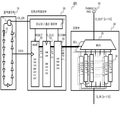
도 3은 본 발명의 일 실시예에 따른 쉬프트레지스터를 이용한 데이터 지연회로를 도시한 블록 구성도이다. 즉, 동작 환경의 변화를 반영하여 변화하는 클럭을 생성하는 클럭발진부(10)로 간단한 링 오실레이터(ring oscillator)를 도시하였다.3 is a block diagram illustrating a data delay circuit using a shift register according to an exemplary embodiment of the present invention. That is, a simple ring oscillator is illustrated as the
도 3을 참조하면, 클럭발진 인에이블 신호(CK_EN)가 하이레벨(로직 ‘1’)로 천이되면 논리곱(11) 로직을 통해 클럭의 발진이 일어난다. 링 오실레이터는 각 버퍼의 지연으로 인하여 신호가 늦게 전파되는 레이스(race)현상을 이용하는 것으로 링 내부에 삽입된 인버터(12)에 의하여 반전된 신호가 지연되어 전파되면서 반전을 일으키며 입력되어 클럭출력(CKO)을 발생시킨다. 이 링오실레이터로 구성된 클럭발진부는 지연부(30)에 사용되는 지연셀의 동작부의 동작환경을 그대로 반영할 수 있도록 버퍼, 인버터 및 별도 지연셀을 사용할 수 있다.Referring to FIG. 3, when the clock oscillation enable signal CK_EN transitions to a high level (logic '1'), a clock oscillation occurs through the logic of the
동작환경의 변화에 따라 클럭발진부에서 발생한 출력클럭(CKO)의 주파수가 변하게 되며, 주파수의 변화는 지연셀의 지연 크기가 얼마나 변했는가를 나타낸다. 도3의 실시예에서 출력클럭(CKO)를 입력받는 지연선택제어부(20)는 내부의 쉬프트레지스터(22)를 구비하여 출력클럭(CKO)에 동기되어 쉬프트레지스터(22)의 값을 쉬프트한다. 쉬프트 레지스터(22)는 클럭 모니터링이 필요없을 경우 모니터갱신제어부에서 출력되는 리셋(RESET) 신호를 입력받아 리셋상태를 유지하며, 모니터링을 위하여 클럭인에이블(CK_EN)이 인에블되면 출력클럭(CKO)가 안정화된 후에 쉬프트레지스터(22)가 쉬프트된다. 클럭인에이블(CK_EN)이 디스에이블되어 출력클럭(CKO)의 발진이 멈추면 쉬프트레지스터(22)의 출력 (SFT_O)은 캡쳐레지스터(23) 클럭(C_CLK)에 동기되어 캡쳐레지스터(23)로 저장되어 캡쳐레지스터(23) 출력신호(CAP_O)를 생성한다. 지연선택제어부(20)은 캡쳐레지스터(23) 출력신호(CAP_O)를 이용하여 지연부(30)에 선택신호를 제공한다. 보정회로(24)는 캡쳐레지스터(23) 출력신호(CAP_O)를 입력받아 최종적인 지연선택신호(COMP_O)를 지연부(30)에 제공한다. 예를 들어, 쉬프트레지스터(22)가 출력클럭(CKO)에 동기되어 쉬프트 될 때, 최하위비트의 레지스터는 리셋값이 로직 ‘1’을 가지며, 입력값은 로직 ‘0’을 갖는다, 최하위비트의 레지스터를 제외한 나머지 쉬프트레지스터는 리셋값이 로직 ‘0’를 가지며 입력값은 앞단의 쉬프트레지스터의 출력을 받는다. 따라서, 출력클럭(CKO)에 동기되어 쉬프트레지스터는 최하위의 로직 ‘1’값을 상위로 쉬프트시키고, 결과적으로 쉬프트레지스터(22)는 단 하나의 레지스터만이 로직 ‘1’을 갖는 다. 이때, 쉬프트레지스터(22)의 출력의 비트수가 2N-bit (N은 자연수)이고, 지연부(30)의 필요한 선택신호(SEL)의 비트수가 N-bit이라면, 보정회로(24)는 최하위비트부터 최상위비트까지 2-bit씩 논리합(OR)를 하여 총 N-bit의 지연선택신호(COMP_O)를 출력하여 지연부(30)의 선택신호(SEL)와 1대 1로 차례대로 연결한다. 이때, N-bit의 지연선택신호(COMP_O) 신호의 최하위비트는 지연부(30) 선택신호(SEL)의 최하위비트와 연결되며, COMP_O의 상위비트들도 차례로 지연부(30)의 선택신호(SEL)의 상위비트들과 차례로 연결한다. 여기서, 지연부(30)의 복수의 지연패스는 선택신호(SEL)의 값이 클수록 큰 지연패스를 선택하도록 하면, 지연부에 입력되는 데이터 입력신호는 다수의 지연패스에 구비된 지연셀의 지연크기 변화와 무관하게 일정한 크기만큼 지연되어 출력된다. 한편. 지연선택신호(COMP_O)와 지연부(30) 선택신호(SEL)의 bit별 연결 순서를 바꾸면 지연셀의 지연크기의 변화와 반대의 지연크기를 갖는 지연패스를 입력신호에 제공할 수 있다.As the operating environment changes, the frequency of the output clock CKO generated by the clock oscillator changes, and the change in frequency indicates how the delay size of the delay cell changes. In the embodiment of FIG. 3, the delay
즉, 지연셀을 선택하는 기준은 지연크기를 동작환경에따라 지연셀 하나를 사용했을 때보다 지연 크기를 작게 만들거나, 반대로 크게 만드는 등의 목적에 따라 보정회로(24)의 구성은 여러가지로 구현가능하다.That is, the criterion for selecting the delay cell may be implemented in various ways in the configuration of the
한편, 쉬프트레지스터(22)의 필요한 비트수를 줄이기위하여 출력클럭(CKO) 와 쉬프트레지스터(22) 입력사이에 클럭분주기(clock divider)를 구비할 수도 있으며, 캡쳐레지스터(23)의 비트수를 줄이기 위하여 상술한 논리합을 이용하거나 논리곱 혹은 반전 등과 같은 논리조합 회로를 쉬프트레지스터(22)의 출력과 캡쳐레지스터(23)사이에 위치시킬 수도 있다.On the other hand, a clock divider may be provided between the output clock CKO and the input of the
도 4는 도 3의 동작신호들의 타이밍 도이다. 4 is a timing diagram of operation signals of FIG. 3.
도 4를 참조하면, 클럭 인에이블 신호(CK_EN)가 하이레벨이 되면 클럭발진기가 발진하여 출력클럭(CKO)를 발생시키고 쉬프트레지스터(22)가 출력클럭(CKO)에 동기되어 쉬프트하면서 최하위 비트는 초기값 로직’1’을 차례로 상위 비트로 쉬프트 된다. 클럭 쉬프트가 종료된 후에 쉬프트 레지스터(22)의 결과값을 보면 일정한 클럭 인에블시간동안 얼마나 클럭이 발생했는지를 알 수 있으며, 이를 기준으로 클럭발진기의 주파수를 예측하고, 지연셀을 선택하는 기준으로 삼는다. 클럭모니터링이 끝나면 클럭인에이블(CK_EN)이 로우레벨(로직’0’)이 되어 클럭 발진이 멈추게 되며, 캡쳐레지스터(23)의 클럭(C_CLK)에 동기되어 쉬프트레지스터(22)의 출력(SFT_O)가 캡쳐레지스터(23)로 저장된다. 보정회로(24)는 캡쳐레지스터(22)의 출력(CAP_O)을 기준으로 보정을 행하여 지연부(30) 선택신호(COMP_O)를 발생시킨다. 보정회로(24)에서 선택신호를 만드는 기준은 상술한 바와 같이 여러가지 목적에 맞게 다양하게 구현이 가능하므로, 동작환경을 목적한대로 보상해주는 다양한 알고리즘(algorithm)이 사용될 수 있다.Referring to FIG. 4, when the clock enable signal CK_EN becomes high, the clock oscillator oscillates to generate the output clock CKO, and the
도 5는 본 발명의 다른 실시예에 따른 카운트레지스터를 이용한 데이터 지연회로를 도시한 블록 구성도이다. 5 is a block diagram illustrating a data delay circuit using a count register according to another exemplary embodiment of the present invention.
도 5를 참조하면, 카운트레지스터(25)를 이용하여 출력클럭(CKO)을 모니터링하면 보정회로(24)에서 카운트레지스터(25)값을 해석하여 지연부(30) 선택신호(SEL)를 생성하게 된다. 도 3과 마찬가지로 클럭 인에이블(CK_EN)이 하이레벨로 천이하면 클럭발진기(10)가 발진하고, 클럭발진기(10)에서 발생한 출력클럭(CKO)에 동기되어 카운트레지스터(25)가 출력클럭(CKO)을 카운트한다. 클럭인에이블(CK_EN)신호가 로우레벨로 천이되면 클럭 모니터링이 종료되며, 캡쳐레지스터(23)가 카운트레지스터(25)의 클럭(C_CLK)에 동기되어 새로운 값으로 저장된다. 보정회로 (24)는 카운터 레지스터(23)의 출력값을 디코딩(decoding)하여 지연부(30) 선택신호(SEL)를 최종적으로 생성한다. 예를 들어 캡쳐레지스터(23)의 비트수가 N-bit (N은 자연수)이고, 지연부의 지연패스가 2N개이고 선택신호의 비트수가 N-bit라면, 캡쳐레지스터(23)의 출력(CAP_O)을 바이패스(bypass)시켜서 지연부(30) 선택신호(SEL)와 1대 1로 연결한다. 캡쳐레지스터(23)의 출력 (CAP_O)의 최하위비트부터 상위비트가 지연부(30) 선택신호(SEL)와 최하위비트부터 상위비트로 차례대로 연결되었을 경우, 지연셀의 지연크기가 작아진 환경에서 클럭발진기의 출력클럭(CKO)의 주파수가 높아진다. 출력클럭(CKO)의 주파수가 높을수록 지연선택신호의 값은 높아지므로, 선택신호의 값이 높을수록 큰 지연을 갖도록 지연부의 지연패스를 구성하면, 동작환경 변화에의하여 줄어든 지연크기를 보상해 줄 수 있다. 반면, 보정회로(24)에서 각 비트의 순서를 역순으로 연결하였을 경우에는 지연크기를 반대로 보상해주는 효과를 얻을 수도 있다.Referring to FIG. 5, when the output clock CKO is monitored using the
보정회로(24)에서 선택신호를 만드는 기준은 상술한 바와 같이 여러가지 목적에 맞게 다양한 논리회로로 구현이 가능하므로, 동작환경을 목적한대로 보상해주는 다양한 알고리즘(algorithm)이 사용될 수 있다.Since the standard for generating the selection signal in the
도 6는 도 5의 동작신호들의 타이밍 도이다.6 is a timing diagram of operation signals of FIG. 5.
도 6을 참조하면, 클럭 인에이블(CK_EN)이 하이레벨이 되면 클럭발진기가 발 진하면서 출력클럭(CKO)를 발생시키고 카운트레지스터(25)가 출력클럭(CKO)에 동기되어 쉬프트하면서 일정시간 내에 발생한 출력클럭(CKO)을 카운트한다. 클럭인에이블(CK_EN)이 로우레벨로 천이된후, 카운트레지스터(25)의 출력값을 확인하면 일정한 클럭인에블 시간동안 발생한 클럭수를 알 수 있으며, 이를 기준으로 클럭발진기의 주파수를 예측하고, 지연셀을 선택하는 기준으로 삼는다. 클럭모니터링이 끝나면 클럭인에이블(CK_EN)이 로우레벨(로직’0’)이 되어 클럭 발진이 멈추게 되며, 캡쳐레지스터(23) 클럭(C_CLK)에 동기되어 카운트레지스터(25)의 출력(CNT_O)이 캡쳐레지스터(23)로 저장된다. 보정회로(24)는 캡쳐레지스터(22)의 출력(CAP_O)을 기준으로 보정을 행하여 보정신호(COMP_O)를 생성하여 지연부(30) 선택신호(SEL)로 연결한다. 보정회로(24)에서 선택신호를 만드는 기준은 상술한 바와 같이 여러가지 목적에 맞게 다양하게 구현이 가능하므로, 동작환경을 목적한대로 보상해주는 다양한 알고리즘(algorithm)이 사용될 수 있다.Referring to FIG. 6, when the clock enable CK_EN becomes high, the clock oscillator oscillates to generate the output clock CKO, and the
도 7은 본 발명의 지연회로를 반도체 칩의 입력패드에 적용된 예를 도시한 블록 구성도이고, 도 8은 본 발명의 지연회로를 반도체 칩의 출력패드에 적용된 예를 도시한 블록 구성도이다.7 is a block diagram illustrating an example in which the delay circuit of the present invention is applied to an input pad of a semiconductor chip, and FIG. 8 is a block diagram illustrating an example in which the delay circuit of the present invention is applied to an output pad of a semiconductor chip.
도 7과 도 8을 참조하면, 반도체 칩간의 지연신호를 고려하여 입력 패드(40)를 거쳐서 들어오는 신호를 원하는 기준으로 지연크기를 보정해주거나, 출력 패드(50)를 통하여 다른 칩으로 전달되는 신호의 지연신호의 크기를 재조정할 필요가 있을 경우에도 마찬가지로 지연신호를 보정해준다. 반도체 칩은 PCB상에서 신호가 전달될 때, 출력패드(50)의 지연, PCB에서의 지연(도시되지 않음), 입력패드(40)의 지연이 누적되어 전달되므로, 지연된 신호의 타이밍이 동작범위에 들지 않으면 제대로 동작하지 않을 수 있다. 따라서, 동작환경에 맞는 지연회로를 입력패드(40) 나 출력패드(50)에 구비하여 동작환경 변화에서 오는 지연신호 때문에 발생하는 불안정한 동작들을 제거할 수 있다. 데이터의 지연크기를 조정하는 방법은 도 3및 도 5에서 상술한 바와 같다. 즉, 본 발명의 지연회로를 사용하면 입력패드(40) 및 출력패드(50)에서 조정이 필요한 데이터 지연크기를 자동으로 의도한대로 조정할 수 있는 특징이 있다. 예를 들어, 칩의 동작환경에 의하여 칩 내부의 지연크기가 커졌을 때, 입력단에서 들어오는 신호가 상대적으로 빠르게 입력될 경우에는 좀더 긴 지연크기를 갖는 지연패스를 선택하도록 할 수 있으며, 반대로 입력단에서 들어오는 신호가 상대적으로 느리게 입력될 경우에는 좀더 작은 지연크기를 갖는 지연패스를 선택하도록 할 수 있게 된다.Referring to FIGS. 7 and 8, in consideration of the delay signal between the semiconductor chips, a signal for correcting the delay size based on a desired reference for a signal input through the
도 9는 본 발명의 외부 쿨링팬(cooling fan) 제어신호를 적용한 예를 도시한 블록 구성도이다. 즉, 지연선택 제어부가 단순 지연부(30) 선택신호만을 생성하는 것이 아니라 보다 적극적으로 반도체 칩의 외부로 출력되어 쿨링팬(cooling fan)(90)과 온도 제어 장치를 제어함으로써 데이터 신호의 지연신호가 원하는 지연크기를 갖을 수 있도록 하는 본 발명의 다른 실시예이다.FIG. 9 is a block diagram illustrating an example in which an external cooling fan control signal of the present invention is applied. That is, the delay selection control unit not only generates the selection signal of the
도 9를 참조하면, 보정회로(24)에서는 클럭발진기의 출력클럭(CKO)을 모니터링하여 지연셀의 선택신호를 생성하는데, 외부에 쿨링팬을 제어하는 신호를 추가로 생성함으로써 동작온도가 일정범위를 유지하도록 하여 온도보상과 지연셀 선택을 조합하여 목적하는 지연신호의 지연크기를 생성할 수 있다. 이와 같이 외부에 쿨링 팬을 부가적으로 제어함으로써, 복수개의 지연셀의 개수를 줄이면서도 의도한대로 입력 데이터 지연크기를 조정할 수 있다.Referring to FIG. 9, the
도 10은 본 발명의 메모리카드의 입출력 데이터의 지연크기를 제어하는 예를 도시한 블록 구성도이다.10 is a block diagram showing an example of controlling the delay size of input / output data of the memory card of the present invention.
도 10을 참조하면, 본 발명의 지연제어 회로를 메모리카드(memory card)(600)에 적용한 실시예이다. 입출력의 지연신호의 지연크기가 호환성 문제로 중요한 관심사가 되는 메모리카드에서는 입출력 신호의 지연크기를 내부적으로 보상해 줌으로써 복잡한 제어를 필요치 않게 한다. 일반적으로 메모리카드 입출력신호에는 데이터신호, 클럭신호, 읽기/쓰기 제어신호등 여러가지 신호들이 있으며, 마찬가지로 제조공정 및 동작전압, 동작온도에 따라서 입출력신호의 지연크기가 달라질 수 있다. 더구나, 메모리카드와 메모리호스트와의 호환성은 매우 중요하기 때문에 여러 회사의 메모리카드 및 여러 회사의 메모리 호스트의 호환성에서 입출력신호의 지연은 안정적인 동작을 보장하는 매우 중요한 요소이다. 본 발명의 지연회로를 메모리카드의 입력 및 출력 패드에 사용하면 매번 CPU가 개입하지 않아도 동작환경을 모니터링하여 자동으로 의도한 지연신호를 생성할 수 있다. 또한, 도 10에서 입력신호에 대한 지연부(30)와 출력신호에 대한 지연부(31)가 별도로 구비하여, 메모리카드 입출력 패드를 통하여 입출력되는 신호에 대하여 메모리카드 내부에서 입력과 출력을 지연신호의 크기를 각각 제어하는 실시예를 도시하였다. 각 입력지연부(30)와 출력지연부(31)는 지연선택제어부(26)에서 발생한 입력 지연선택신호(SEL_IN) 및 출력 지연선택신호(SEL_OUT)를 이용하여 각 입력신호 및 출력신호의 지연크기를 조정하며, 조정방법은 도 3및 도 5에서 상술한 바와 같이 제어한다.Referring to FIG. 10, the delay control circuit of the present invention is applied to a
도 11은 본 발명의 데이터 지연 동작을 도식화한 플로우차트이다.11 is a flowchart illustrating the data delay operation of the present invention.
도 11을 참조하면, 제어신호의 전원이 인가된 후, 동작환경의 변화가 발생하여 지연부 선택신호의 갱신이 필요하다고 판단(720)되면 동작환경의 변화를 클럭발진기의 주파수를 이용하여 측정한다.(730) 측정이 완료되면, 동작환경의 변화량을 지연부의 제어신호로 변환한다.(740) 생성된 지연부 제어신호를 지연부의 복수의 지연패스 중 하나를 선택하도록 지연부 선택신호와 연결한다.(750) 선택된 지연패스를 거쳐서 데이터 신호가 지연된다.(760) 동작중 환경이 변화하여 지연선택신호의 갱신이 필요할 경우 마찬가지 과정을 되풀이한다.Referring to FIG. 11, when it is determined that a change in the operating environment occurs and an update of the delay selection signal is necessary after the power of the control signal is applied (720), the change in the operating environment is measured using the frequency of the clock oscillator. When the measurement is completed, the change amount of the operating environment is converted into a control signal of the delay unit. (740) The generated delay unit control signal is connected to the delay unit selection signal to select one of a plurality of delay paths of the delay unit. (750) The data signal is delayed through the selected delay path. (760) The same process is repeated when the environment is changed and the delay selection signal needs to be updated.
도 12는 본발명의 하나의 실시예를 이용한 데이터 지연 방법을 구체적으로 도식화한 플로우챠트이다.12 is a flowchart specifically illustrating a data delay method using an embodiment of the present invention.
도 12를 참조하면, 지연부 선택신호의 갱신이 필요하다고 판단(820)되면 클럭발진기의 클럭 주파수 모니터링 회로를 초기화하고, 클럭발진기를 인에이블 시킨다(830). 클럭발진기의 출력클럭의 주파수 모니터링이 끝나면(840), 클럭발진기를 디스에이블 시키고(850)하고, 캡쳐 레지스터를 갱신한다.(860) 캡쳐레지스터의 출력을 기준으로 보정을 수행하고(870) 지연선택신호를 생성한다.(880) 이후 동작중 환경이 변화하여 지연선택신호의 갱신이 필요할 경우 마찬가지 과정을 되풀이한다.Referring to FIG. 12, if it is determined that an update of the delay select signal is necessary (820), the clock frequency monitoring circuit of the clock oscillator is initialized and the clock oscillator is enabled (830). When the frequency monitoring of the output clock of the clock oscillator is finished (840), the clock oscillator is disabled (850) and the capture register is updated (860). The correction is performed based on the output of the capture register (870) and delay selection is performed. In operation 880, if the environment changes during the operation and the delay selection signal needs to be updated, the same process is repeated.
이상과 같이 본 발명은 동작환경의 변화를 반영하는 클럭을 생성하는 클럭발진기를 사용하여 복수의 지연패스들 중에서 원하는 지연패스를 자동으로 선택하게 하는 데이터 지연크기 제어를 가능하게 한다.As described above, the present invention enables a data delay size control to automatically select a desired delay path among a plurality of delay paths by using a clock oscillator for generating a clock reflecting a change in an operating environment.
이상 도면과 명세서에서 최적 실시예가 개시되었다. 여기서 특정한 용어들이 사용되었으나, 이는 단지 본 발명을 설명하기 위한 목적에서 사용된 것이지 의미한정이나 특허청구범위에 기재된 본 발명의 범위를 제한하기 위하여 사용된 것은 아니다. 그러므로 본 기술 분야의 통상의 지식을 가진 자라면 이로부터 다양한 변형 및 균등한 타 실시예가 가능하다는 점을 이해할 것이다. 따라서, 본 발명의 진정한 기술적 보호 범위는 첨부된 특허청구범위의 기술적 사상에 의해 정해져야 할 것이다.The best embodiment has been disclosed in the drawings and specification above. Although specific terms have been used herein, they are used only for the purpose of describing the present invention and are not intended to limit the scope of the invention as defined in the claims or the claims. Therefore, those skilled in the art will understand that various modifications and equivalent other embodiments are possible from this. Therefore, the true technical protection scope of the present invention will be defined by the technical spirit of the appended claims.
상기에서 살펴본 본 발명은 반도체 장치의 반도체 칩 설계시 칩의 동작 환경(온도, 전압, 제조공정)의 변화에 상관없이 예상된 지연값을 생성하는 효과가 있으며, 선택적으로 외부 시스템과 인터페이스 조건을 조정할 수 있는 효과가 있다. 이를 통해 다양한 동작 모드 및 환경에서도 신뢰성있는 제품의 제작이 가능하다.The present invention as described above has the effect of generating the expected delay value regardless of the change in the operating environment (temperature, voltage, manufacturing process) of the chip when designing the semiconductor chip of the semiconductor device, and selectively adjusts the interface conditions with the external system It can be effective. This enables the production of reliable products in various operating modes and environments.
Claims (21)
Priority Applications (4)
| Application Number | Priority Date | Filing Date | Title |
|---|---|---|---|
| KR1020060009805A KR100675009B1 (en) | 2006-02-01 | 2006-02-01 | Data Delay Control Circuits and Methods |
| US11/669,296 US7696802B2 (en) | 2006-02-01 | 2007-01-31 | Data delay control circuit and method |
| CNA2007100079422A CN101013883A (en) | 2006-02-01 | 2007-02-01 | Data delay control circuit and method |
| US12/726,565 US8305127B2 (en) | 2006-02-01 | 2010-03-18 | Data delay control circuit and method |
Applications Claiming Priority (1)
| Application Number | Priority Date | Filing Date | Title |
|---|---|---|---|
| KR1020060009805A KR100675009B1 (en) | 2006-02-01 | 2006-02-01 | Data Delay Control Circuits and Methods |
Publications (1)
| Publication Number | Publication Date |
|---|---|
| KR100675009B1 true KR100675009B1 (en) | 2007-01-29 |
Family
ID=38014998
Family Applications (1)
| Application Number | Title | Priority Date | Filing Date |
|---|---|---|---|
| KR1020060009805A Expired - Fee Related KR100675009B1 (en) | 2006-02-01 | 2006-02-01 | Data Delay Control Circuits and Methods |
Country Status (3)
| Country | Link |
|---|---|
| US (2) | US7696802B2 (en) |
| KR (1) | KR100675009B1 (en) |
| CN (1) | CN101013883A (en) |
Families Citing this family (14)
| Publication number | Priority date | Publication date | Assignee | Title |
|---|---|---|---|---|
| KR100675009B1 (en) * | 2006-02-01 | 2007-01-29 | 삼성전자주식회사 | Data Delay Control Circuits and Methods |
| US7508250B1 (en) | 2008-07-28 | 2009-03-24 | International Business Machines Corporation | Testing for normal or reverse temperature related delay variations in integrated circuits |
| JP5304280B2 (en) * | 2009-01-30 | 2013-10-02 | 株式会社ニコン | Phase adjusting device and camera |
| US8683164B2 (en) * | 2009-02-04 | 2014-03-25 | Micron Technology, Inc. | Stacked-die memory systems and methods for training stacked-die memory systems |
| CN102117094A (en) * | 2009-12-31 | 2011-07-06 | 张永 | Chip speed self-adaptive technical scheme |
| TWI459721B (en) * | 2012-01-03 | 2014-11-01 | Global Unichip Corp | Gated voltage controlled oscillator and clock and data recovery circuit |
| KR101418045B1 (en) * | 2013-01-18 | 2014-07-14 | 연세대학교 산학협력단 | Temperature sensor and temperature sensing method |
| JP6237310B2 (en) * | 2014-02-14 | 2017-11-29 | 株式会社ソシオネクスト | Semiconductor integrated circuit |
| CN104934058B (en) * | 2014-03-17 | 2018-12-04 | 中芯国际集成电路制造(上海)有限公司 | Temperature-compensating delay circuit for EEPROM |
| JP6764299B2 (en) * | 2016-09-30 | 2020-09-30 | ルネサスエレクトロニクス株式会社 | Semiconductor device |
| CN111596192B (en) * | 2019-02-21 | 2023-03-24 | 中芯国际集成电路制造(上海)有限公司 | Measuring circuit and measuring method thereof |
| KR102747274B1 (en) * | 2019-12-27 | 2024-12-26 | 엘지디스플레이 주식회사 | Display apparatus |
| TWI757819B (en) | 2020-08-06 | 2022-03-11 | 華邦電子股份有限公司 | Delay control device and tunable delay device |
| CN115549657B (en) * | 2022-10-21 | 2025-08-22 | 长鑫存储技术有限公司 | Oscillation circuit and memory |
Citations (8)
| Publication number | Priority date | Publication date | Assignee | Title |
|---|---|---|---|---|
| JPH1083677A (en) | 1996-09-09 | 1998-03-31 | Hitachi Ltd | Semiconductor storage device and semiconductor integrated circuit |
| KR19980056179A (en) * | 1996-12-28 | 1998-09-25 | 김영환 | Sense Amplifier Enable Signal Generation Circuit of Semiconductor Memory Devices |
| KR20020055160A (en) * | 2000-12-28 | 2002-07-08 | 박종섭 | Bit-line sensing start timing control device |
| KR20040058532A (en) * | 2002-12-27 | 2004-07-05 | 주식회사 하이닉스반도체 | Delay circuit |
| JP2004364252A (en) | 2003-05-31 | 2004-12-24 | Hynix Semiconductor Inc | Digital delay-locked loop |
| KR20050052716A (en) * | 2003-12-01 | 2005-06-07 | 주식회사 하이닉스반도체 | Semiconductor device having an automatic controlled delay circuit and method therefor |
| KR20050076202A (en) * | 2004-01-20 | 2005-07-26 | 삼성전자주식회사 | Dleay signal generator circuit and memory system including the same |
| KR20050116708A (en) * | 2004-06-08 | 2005-12-13 | 삼성전자주식회사 | Semiconductor memory device controlling sense amplifying time according to bitline leakage current and drving method of the same |
Family Cites Families (9)
| Publication number | Priority date | Publication date | Assignee | Title |
|---|---|---|---|---|
| US5087842A (en) | 1988-01-06 | 1992-02-11 | Digital Equipment Corporation | Delay circuit having one of a plurality of delay lines which may be selected to provide an operation of a ring oscillator |
| US5561692A (en) * | 1993-12-09 | 1996-10-01 | Northern Telecom Limited | Clock phase shifting method and apparatus |
| JP2000357951A (en) * | 1999-06-15 | 2000-12-26 | Mitsubishi Electric Corp | Delay circuit, clock generation circuit, and phase synchronization circuit |
| KR100393217B1 (en) | 2001-03-09 | 2003-07-31 | 삼성전자주식회사 | Memory module having control circuit for operating memory devices and data buffer by same clock frequency |
| CN1393992A (en) * | 2001-07-02 | 2003-01-29 | 朗迅科技公司 | Delay compensating circuit containing feedback loop |
| JP2003023343A (en) | 2001-07-10 | 2003-01-24 | Mitsubishi Electric Corp | Delay signal generation circuit |
| JP2003216269A (en) | 2002-01-18 | 2003-07-31 | Mitsubishi Electric Corp | Semiconductor device |
| CN100465847C (en) | 2004-03-31 | 2009-03-04 | 华为技术有限公司 | Fan speed control method |
| KR100675009B1 (en) * | 2006-02-01 | 2007-01-29 | 삼성전자주식회사 | Data Delay Control Circuits and Methods |
-
2006
- 2006-02-01 KR KR1020060009805A patent/KR100675009B1/en not_active Expired - Fee Related
-
2007
- 2007-01-31 US US11/669,296 patent/US7696802B2/en not_active Expired - Fee Related
- 2007-02-01 CN CNA2007100079422A patent/CN101013883A/en active Pending
-
2010
- 2010-03-18 US US12/726,565 patent/US8305127B2/en not_active Expired - Fee Related
Patent Citations (8)
| Publication number | Priority date | Publication date | Assignee | Title |
|---|---|---|---|---|
| JPH1083677A (en) | 1996-09-09 | 1998-03-31 | Hitachi Ltd | Semiconductor storage device and semiconductor integrated circuit |
| KR19980056179A (en) * | 1996-12-28 | 1998-09-25 | 김영환 | Sense Amplifier Enable Signal Generation Circuit of Semiconductor Memory Devices |
| KR20020055160A (en) * | 2000-12-28 | 2002-07-08 | 박종섭 | Bit-line sensing start timing control device |
| KR20040058532A (en) * | 2002-12-27 | 2004-07-05 | 주식회사 하이닉스반도체 | Delay circuit |
| JP2004364252A (en) | 2003-05-31 | 2004-12-24 | Hynix Semiconductor Inc | Digital delay-locked loop |
| KR20050052716A (en) * | 2003-12-01 | 2005-06-07 | 주식회사 하이닉스반도체 | Semiconductor device having an automatic controlled delay circuit and method therefor |
| KR20050076202A (en) * | 2004-01-20 | 2005-07-26 | 삼성전자주식회사 | Dleay signal generator circuit and memory system including the same |
| KR20050116708A (en) * | 2004-06-08 | 2005-12-13 | 삼성전자주식회사 | Semiconductor memory device controlling sense amplifying time according to bitline leakage current and drving method of the same |
Also Published As
| Publication number | Publication date |
|---|---|
| US7696802B2 (en) | 2010-04-13 |
| US8305127B2 (en) | 2012-11-06 |
| CN101013883A (en) | 2007-08-08 |
| US20070176661A1 (en) | 2007-08-02 |
| US20100182064A1 (en) | 2010-07-22 |
Similar Documents
| Publication | Publication Date | Title |
|---|---|---|
| US7696802B2 (en) | Data delay control circuit and method | |
| JP4450586B2 (en) | Semiconductor integrated circuit | |
| JP5579979B2 (en) | Semiconductor device, internal signal timing circuit, and delay time measuring method | |
| TWI473113B (en) | Duty cycle correction circuit and semiconductor integrated circuit apparatus including the same | |
| JP4416580B2 (en) | Delay control device | |
| KR101811133B1 (en) | Reception circuit, method for adjusting timing in reception circuit, and semiconductor device | |
| US8856578B2 (en) | Integrated circuit device including skew adjustment circuit and skew adjustment method | |
| US7889581B2 (en) | Digital DLL circuit | |
| US20100052739A1 (en) | Device and control method of device | |
| US7574638B2 (en) | Semiconductor device tested using minimum pins and methods of testing the same | |
| US8008967B2 (en) | Power supply voltage adjusting device | |
| JP5331902B2 (en) | Signal restoration circuit, latency adjustment circuit, memory controller, processor, computer, signal restoration method, and latency adjustment method | |
| CN1818688B (en) | System including an operating speed detection apparatus, an operating speed detection apparatus and method thereof | |
| US7586351B2 (en) | Apparatus and method for controlling delay of signal | |
| JP5673842B2 (en) | Semiconductor device | |
| JP5005928B2 (en) | Interface circuit and storage control device including the interface circuit | |
| JP2012100058A (en) | Delay circuit, delay control device, memory control device and information terminal apparatus | |
| US8194496B2 (en) | Circuit and method for recovering clock data in highly integrated semiconductor memory apparatus | |
| JP4248074B2 (en) | System having an operation timing control function | |
| JP2011150759A (en) | Memory interface circuit, semiconductor device, and memory interface method | |
| JP3776895B2 (en) | Phase adjustment circuit | |
| JP2012044489A (en) | Skew adjusting circuit | |
| KR100557573B1 (en) | Semiconductor memory device | |
| JP2008022466A (en) | Clock generating circuit |
Legal Events
| Date | Code | Title | Description |
|---|---|---|---|
| A201 | Request for examination | ||
| PA0109 | Patent application |
St.27 status event code: A-0-1-A10-A12-nap-PA0109 |
|
| PA0201 | Request for examination |
St.27 status event code: A-1-2-D10-D11-exm-PA0201 |
|
| D13-X000 | Search requested |
St.27 status event code: A-1-2-D10-D13-srh-X000 |
|
| D14-X000 | Search report completed |
St.27 status event code: A-1-2-D10-D14-srh-X000 |
|
| E701 | Decision to grant or registration of patent right | ||
| PE0701 | Decision of registration |
St.27 status event code: A-1-2-D10-D22-exm-PE0701 |
|
| GRNT | Written decision to grant | ||
| PR0701 | Registration of establishment |
St.27 status event code: A-2-4-F10-F11-exm-PR0701 |
|
| PR1002 | Payment of registration fee |
St.27 status event code: A-2-2-U10-U11-oth-PR1002 Fee payment year number: 1 |
|
| PG1601 | Publication of registration |
St.27 status event code: A-4-4-Q10-Q13-nap-PG1601 |
|
| PR1001 | Payment of annual fee |
St.27 status event code: A-4-4-U10-U11-oth-PR1001 Fee payment year number: 4 |
|
| PR1001 | Payment of annual fee |
St.27 status event code: A-4-4-U10-U11-oth-PR1001 Fee payment year number: 5 |
|
| FPAY | Annual fee payment |
Payment date: 20111229 Year of fee payment: 6 |
|
| PR1001 | Payment of annual fee |
St.27 status event code: A-4-4-U10-U11-oth-PR1001 Fee payment year number: 6 |
|
| R18-X000 | Changes to party contact information recorded |
St.27 status event code: A-5-5-R10-R18-oth-X000 |
|
| FPAY | Annual fee payment |
Payment date: 20130102 Year of fee payment: 7 |
|
| PR1001 | Payment of annual fee |
St.27 status event code: A-4-4-U10-U11-oth-PR1001 Fee payment year number: 7 |
|
| LAPS | Lapse due to unpaid annual fee | ||
| PC1903 | Unpaid annual fee |
St.27 status event code: A-4-4-U10-U13-oth-PC1903 Not in force date: 20140123 Payment event data comment text: Termination Category : DEFAULT_OF_REGISTRATION_FEE |
|
| PC1903 | Unpaid annual fee |
St.27 status event code: N-4-6-H10-H13-oth-PC1903 Ip right cessation event data comment text: Termination Category : DEFAULT_OF_REGISTRATION_FEE Not in force date: 20140123 |