KR100655082B1 - Phase change memory device and manufacturing method thereof - Google Patents
Phase change memory device and manufacturing method thereof Download PDFInfo
- Publication number
- KR100655082B1 KR100655082B1 KR1020050128477A KR20050128477A KR100655082B1 KR 100655082 B1 KR100655082 B1 KR 100655082B1 KR 1020050128477 A KR1020050128477 A KR 1020050128477A KR 20050128477 A KR20050128477 A KR 20050128477A KR 100655082 B1 KR100655082 B1 KR 100655082B1
- Authority
- KR
- South Korea
- Prior art keywords
- phase change
- contact
- lower electrode
- contact plug
- memory device
- Prior art date
- Legal status (The legal status is an assumption and is not a legal conclusion. Google has not performed a legal analysis and makes no representation as to the accuracy of the status listed.)
- Expired - Fee Related
Links
Images


Classifications
-
- H—ELECTRICITY
- H10—SEMICONDUCTOR DEVICES; ELECTRIC SOLID-STATE DEVICES NOT OTHERWISE PROVIDED FOR
- H10N—ELECTRIC SOLID-STATE DEVICES NOT OTHERWISE PROVIDED FOR
- H10N70/00—Solid-state devices having no potential barriers, and specially adapted for rectifying, amplifying, oscillating or switching
- H10N70/20—Multistable switching devices, e.g. memristors
- H10N70/231—Multistable switching devices, e.g. memristors based on solid-state phase change, e.g. between amorphous and crystalline phases, Ovshinsky effect
-
- H—ELECTRICITY
- H10—SEMICONDUCTOR DEVICES; ELECTRIC SOLID-STATE DEVICES NOT OTHERWISE PROVIDED FOR
- H10B—ELECTRONIC MEMORY DEVICES
- H10B63/00—Resistance change memory devices, e.g. resistive RAM [ReRAM] devices
- H10B63/30—Resistance change memory devices, e.g. resistive RAM [ReRAM] devices comprising selection components having three or more electrodes, e.g. transistors
-
- H—ELECTRICITY
- H10—SEMICONDUCTOR DEVICES; ELECTRIC SOLID-STATE DEVICES NOT OTHERWISE PROVIDED FOR
- H10N—ELECTRIC SOLID-STATE DEVICES NOT OTHERWISE PROVIDED FOR
- H10N70/00—Solid-state devices having no potential barriers, and specially adapted for rectifying, amplifying, oscillating or switching
- H10N70/011—Manufacture or treatment of multistable switching devices
- H10N70/061—Shaping switching materials
- H10N70/063—Shaping switching materials by etching of pre-deposited switching material layers, e.g. lithography
-
- H—ELECTRICITY
- H10—SEMICONDUCTOR DEVICES; ELECTRIC SOLID-STATE DEVICES NOT OTHERWISE PROVIDED FOR
- H10N—ELECTRIC SOLID-STATE DEVICES NOT OTHERWISE PROVIDED FOR
- H10N70/00—Solid-state devices having no potential barriers, and specially adapted for rectifying, amplifying, oscillating or switching
- H10N70/801—Constructional details of multistable switching devices
- H10N70/821—Device geometry
- H10N70/826—Device geometry adapted for essentially vertical current flow, e.g. sandwich or pillar type devices
-
- H—ELECTRICITY
- H10—SEMICONDUCTOR DEVICES; ELECTRIC SOLID-STATE DEVICES NOT OTHERWISE PROVIDED FOR
- H10N—ELECTRIC SOLID-STATE DEVICES NOT OTHERWISE PROVIDED FOR
- H10N70/00—Solid-state devices having no potential barriers, and specially adapted for rectifying, amplifying, oscillating or switching
- H10N70/801—Constructional details of multistable switching devices
- H10N70/841—Electrodes
- H10N70/8418—Electrodes adapted for focusing electric field or current, e.g. tip-shaped
-
- H—ELECTRICITY
- H10—SEMICONDUCTOR DEVICES; ELECTRIC SOLID-STATE DEVICES NOT OTHERWISE PROVIDED FOR
- H10N—ELECTRIC SOLID-STATE DEVICES NOT OTHERWISE PROVIDED FOR
- H10N70/00—Solid-state devices having no potential barriers, and specially adapted for rectifying, amplifying, oscillating or switching
- H10N70/801—Constructional details of multistable switching devices
- H10N70/881—Switching materials
- H10N70/882—Compounds of sulfur, selenium or tellurium, e.g. chalcogenides
- H10N70/8825—Selenides, e.g. GeSe
-
- H—ELECTRICITY
- H10—SEMICONDUCTOR DEVICES; ELECTRIC SOLID-STATE DEVICES NOT OTHERWISE PROVIDED FOR
- H10N—ELECTRIC SOLID-STATE DEVICES NOT OTHERWISE PROVIDED FOR
- H10N70/00—Solid-state devices having no potential barriers, and specially adapted for rectifying, amplifying, oscillating or switching
- H10N70/801—Constructional details of multistable switching devices
- H10N70/881—Switching materials
- H10N70/882—Compounds of sulfur, selenium or tellurium, e.g. chalcogenides
- H10N70/8828—Tellurides, e.g. GeSbTe
-
- G—PHYSICS
- G11—INFORMATION STORAGE
- G11C—STATIC STORES
- G11C2213/00—Indexing scheme relating to G11C13/00 for features not covered by this group
- G11C2213/50—Resistive cell structure aspects
- G11C2213/52—Structure characterized by the electrode material, shape, etc.
Landscapes
- Engineering & Computer Science (AREA)
- Manufacturing & Machinery (AREA)
- Semiconductor Memories (AREA)
Abstract
본 발명은 상변화 메모리 소자 및 그 제조방법에 관한 것이다. 본 발명에서는, 상변화 메모리 소자의 하부전극과 상변화 물질막 사이에 구비되는 콘택 플러그를 형성함에 있어서, 상변화 물질막과 접하는 탑 영역에 비해 하부전극과 접하는 바텀 영역의 면적을 보다 크게 구현함을 특징으로 한다. 그 결과, 상기 콘택 플러그와 접하고 있는 상변화 물질막에 대해서는 전류 밀도가 증가하여 구동시 전력 소모를 최소화할 수 있게 된다. 그리고, 콘택 플러그의 바텀 영역과 하부전극과의 접촉 계면에서는 오믹 콘택 효과가 향상되어 상변화 메모리 소자의 리세트 및 세트 동작 특성이 보다 향상된다. 또한, 탑 영역에 비해 바텀 영역의 면적이 보다 넓은 상기 콘택 플러그의 구조적 특징으로 인해 층간절연막 사이에 콘택 플러그가 단단히 고정된다. 따라서, 후속의 공정 또는 외부의 물리적인 힘에 의해 콘택 플러그를 구성하는 도전물이 들뜨거나 이탈되는 문제점이 해소된다.The present invention relates to a phase change memory device and a method of manufacturing the same. In the present invention, in forming a contact plug provided between the bottom electrode and the phase change material film of the phase change memory device, the area of the bottom area in contact with the bottom electrode is larger than that of the top area in contact with the phase change material film. It is characterized by. As a result, the current density increases with respect to the phase change material film in contact with the contact plug, thereby minimizing power consumption during driving. The ohmic contact effect is improved at the contact interface between the bottom region of the contact plug and the lower electrode, thereby further improving the reset and set operation characteristics of the phase change memory device. In addition, the contact plug is firmly fixed between the interlayer insulating films due to the structural feature of the contact plug having a larger area of the bottom region than the top region. Therefore, the problem that the conductive material constituting the contact plug is lifted or released by a subsequent process or an external physical force is solved.
Description
도 1a 및 도 1b는 종래 기술에 따른 상변화 메모리 소자의 단면구조를 나타낸다. 1A and 1B show a cross-sectional structure of a phase change memory device according to the prior art.
도 2는 상변화 메모리 소자의 메모리 셀 어레이를 나타낸다.2 illustrates a memory cell array of a phase change memory device.
도 3은 메모리 셀 어레이를 구성하는 상변화 메모리 소자의 구조를 나타낸다.3 illustrates a structure of a phase change memory device constituting a memory cell array.
도 4는 상변화 메모리 소자에 적용된 상변화 물질막의 온도 및 시간에 대한 결정 구조 변화 곡선을 나타낸다. 4 illustrates a crystal structure change curve with respect to temperature and time of a phase change material film applied to a phase change memory device.
도 5는 본 발명의 실시예에 따른 상변화 메모리 소자의 단면구조를 나타낸다.5 illustrates a cross-sectional structure of a phase change memory device according to an embodiment of the present invention.
도 6a 내지 도 6h는 본 발명의 실시예에 따른 상변화 메모리 소자의 제조방법을 순차적으로 나타내는 단면도들이다.6A through 6H are cross-sectional views sequentially illustrating a method of manufacturing a phase change memory device according to an exemplary embodiment of the present invention.
도 7a 내지 도 7c는 본 발명의 또 다른 실시예에 따른 상변화 메모리 소자의 제조방법을 순차적으로 나타내는 단면도들이다.7A to 7C are cross-sectional views sequentially illustrating a method of manufacturing a phase change memory device according to still another embodiment of the present invention.
< 도면의 주요 부분에 대한 부호의 설명 ><Description of Symbols for Main Parts of Drawings>
200: 반도체 기판 202: 하부전극200: semiconductor substrate 202: lower electrode
204: 제1층간절연막 206: 제2층간절연막204: first interlayer insulating film 206: second interlayer insulating film
208: 포토 마스크 패턴 210: 개구208: photo mask pattern 210: opening
214: 제1콘택홀 218: 제2콘택홀214: first contact hole 218: second contact hole
220: 콘택 플러그홀 222: 도전물220: contact plug hole 222: conductive material
224: 콘택 플러그 226,226a: 상변화 물질막224: contact plug 226,226a: phase change material film
228,228a: 도전막(하부전극) 230,230a: 산화막228,228a: conductive film (lower electrode) 230,230a: oxide film
본 발명은 반도체 메모리 소자 및 그 제조방법에 관한 것으로서, 보다 상세하게는 상변화 메모리 소자 및 그 제조방법에 관한 것이다.The present invention relates to a semiconductor memory device and a method of manufacturing the same, and more particularly, to a phase change memory device and a method of manufacturing the same.
데이터를 저장하기 위해 사용되는 반도체 메모리 소자들은 일반적으로 휘발성 메모리 소자와 비휘발성 메모리 소자로 구분될 수 있다. 먼저 DRAM(Dynamic Random Access Memory)이나 SRAM(Static Rrandom Access Memory)으로 대표되는 휘발성 메모리 소자는 데이터의 입출력 동작은 빠르지만 전원 공급이 중단됨에 따라 저장된 데이터를 소실하는 특성이 있다. 또한, 상기 디램은 주기적인 리프레쉬 동작이 필요하며, 높은 저하 저장능력이 요구된다. 따라서, 디램 소자의 경우에는 캐패시턴스를 증가시키기 위해 많은 노력들이 시도되고 있다. 그 예로서, 캐패시터의 하부전극의 표면적을 증가시켜 캐패시턴스를 증가시키는 방법이 보편적으로 실시되고 있기는 하나, 하부전극의 표면적을 증가시킴에 따라 디램 소자의 집적도가 저하되는 단점이 있다.Semiconductor memory devices used to store data may be generally classified into volatile memory devices and nonvolatile memory devices. First, a volatile memory device represented by DRAM (Dynamic Random Access Memory) or SRAM (Static Rrandom Access Memory) has a characteristic of fast data input / output operation but loss of stored data as power supply is interrupted. In addition, the DRAM requires a periodic refresh operation and a high degradation storage capacity. Therefore, many efforts have been made to increase capacitance in the case of DRAM devices. For example, although a method of increasing capacitance by increasing the surface area of the lower electrode of the capacitor is generally practiced, there is a disadvantage in that the integration degree of the DRAM device decreases as the surface area of the lower electrode is increased.
한편, 이이피롬(Electrically Erasable Programmable Read Only Memory)을 기반으로 하는 낸드(NAND) 또는 노아(NOR) 타입의 플래쉬 메모리로 대표되는 비휘발성 메모리 소자는 전원 공급이 중단되더라도 데이터가 그대로 유지되는 특성이 있다. 이러한 비휘발성 메모리 소자들은 반도체 기판에 차례로 적층된 게이트 절연막, 부유게이트, 유전체막 및 제어게이트로 구성된 게이트 패턴을 갖는다. 그리고, 이러한 비휘발성 메모리 소자에 데이터를 기입 및 소거하는 원리는 게이트 절연막을 통하여 전하를 터널링시키는 방법을 사용하는데, 이때 전원전압에 비하여 높은 동작 전압이 요구된다. 이로 인하여, 플래쉬 기억 소자들은 기입동작 및 소거동작에 필요한 전압을 형성하기 위한 승압 회로가 요구되는 바, 디자인룰을 증가시킨다는 취약점을 가지고 있다. On the other hand, nonvolatile memory devices represented by NAND or NOR flash memory based on an electrically erasable programmable read only memory have a characteristic that data is retained even when the power supply is interrupted. . Such nonvolatile memory devices have a gate pattern including a gate insulating film, a floating gate, a dielectric film, and a control gate, which are sequentially stacked on a semiconductor substrate. In addition, the principle of writing and erasing data in such a nonvolatile memory device uses a method of tunneling charges through a gate insulating layer, which requires a higher operating voltage than a power supply voltage. For this reason, the flash memory devices have a vulnerability in that they require a boost circuit for forming voltages required for the write operation and the erase operation, thereby increasing the design rule.
따라서, 정보 통신 분야의 급속한 발달과 컴퓨터와 같은 정보 매체의 급속한 대중화에 따라 그 기능적인 면에 있어서 초고속 동작이 가능하고 대용량의 메모리 저장 능력을 가지는 차세대 반도체 메모리 소자에 대한 수요가 점차 증가하고 있다. 차세대 반도체 메모리 소자는 디램등의 휘발성 메모리 소자 및 플래쉬 메모리등의 비휘발성 메모리 소자의 장점을 취하여 개발된 것이다. 따라서, 구동시 전력 소모량이 적으면서도 데이터의 유지 및 리드/라이트 동작 특성이 우수하다는 장점이 있다. 이러한 차세대 반도체 메모리 소자로서는, FRAM(Ferroelectric Random Access Memory), MRAM(Magnetic Random Access Memory), PRAM(Phase-change Random Access Memory) 또는 NFGM등이 있다.Therefore, with the rapid development of the information communication field and the rapid popularization of information media such as computers, the demand for next-generation semiconductor memory devices capable of ultra-fast operation in terms of their functionalities and having a large memory storage capacity is increasing. Next-generation semiconductor memory devices are developed by taking advantage of volatile memory devices such as DRAM and nonvolatile memory devices such as flash memory. Accordingly, there is an advantage in that the data retention and the read / write operation characteristics are excellent while the power consumption is small while driving. Such next-generation semiconductor memory devices include ferroelectric random access memory (FRAM), magnetic random access memory (MRAM), phase-change random access memory (PRAM), and NFGM.
상기한 차세대 메모리 소자중 특히 상기 PRAM(상변화 메모리 소자)은 단순한 구조를 가지면서도 저렴한 비용으로 고집적화를 이룰 수 있으며, 고속 동작이 가능하다는 장점으로 인해 최근들어 가장 주목받는 차세대 메모리 소자중의 하나로 떠오르고 있다. 이러한 상변화 기억 소자에서의 데이터 저장은 상변화 물질막의 결정 구조 변화에 의한 저항 차이를 이용하여 이루어진다. 이러한 상변화 물질로서는, 게르마늄(Ge), 안티몬(Sb) 및 텔루늄(Te)으로 구성된 칼코겐 화합물(GST: Ge-Sb-Te)이 사용될 수 있는데, 상변화 물질은 공급되는 전류의 크기 및 공급 시간에 의존하여 결정 구조가 달라진다. 즉, 상변화 물질막에 높은 크기의 전류 펄스를 단시간 인가하여 상변화 물질막의 온도를 용융점 부근까지 높인 후, 급냉(약 1ns 미만)시키면 열을 받은 상변화 물질막 부분은 저항이 높은 비정질 상태로 된다(리세트). 반면, 상대적으로 낮은 크기의 전류 펄스를 장시간 인가하여 상변화 물질막의 온도를 용융 온도보다 낮은 결정화 온도로 유지하여 결정화시킨 후, 냉각시키면 열을 받은 상변화 물질막 부분은 저항이 낮은 결정 상태가 된다(세트).Among the above-mentioned next-generation memory devices, the PRAM (phase change memory device), in particular, has a simple structure and can be highly integrated at a low cost. have. Data storage in such a phase change memory device is made using a difference in resistance due to a change in crystal structure of the phase change material film. As the phase change material, a chalcogenide compound (GST: Ge-Sb-Te) composed of germanium (Ge), antimony (Sb), and tellurium (Te) may be used. The crystal structure depends on the feeding time. That is, by applying a high current pulse to the phase change material film for a short time to increase the temperature of the phase change material film to near the melting point, and then rapidly cooling (less than about 1 ns), the phase change material film portion subjected to heat becomes amorphous in a high resistance state. (Reset). On the other hand, when a relatively low magnitude current pulse is applied for a long time, the temperature of the phase change material film is kept at a crystallization temperature lower than the melting temperature and crystallized. (set).
이처럼, 상변화 물질막은 그 결정 구조에 따라서 저항의 크기가 달라지는 특성(결정 상태는 저항이 작고, 비정질 상태는 저항이 크다)을 가지며, 이러한 특성을 이용하여 "1" 또는 "0"의 데이터를 프로그램하고 소거하게 되는 것이다. 이러한 상변화 메모리 소자에 대한 구조 및 그 제조과정이 미국특허 6,936,840호 또는 6,908,812호등에 제시되어 있다.As described above, the phase change material film has a characteristic in which the magnitude of the resistance varies depending on the crystal structure (the crystal state is small in resistance, and the amorphous state is large in resistance), and the data of "1" or "0" is used using this characteristic. It will be programmed and erased. The structure of the phase change memory device and its fabrication process are disclosed in US Pat. No. 6,936,840 or 6,908,812.
하기 도 1a 및 도 1b에는 종래 기술에 따른 상변화 메모리 소자의 단면구조가 도시되어 있다.1A and 1B illustrate a cross-sectional structure of a phase change memory device according to the prior art.
먼저, 도 1a를 참조하면, 예컨대 p타입(또는 n타입)의 반도체 기판(10) 상부에 하부전극(12)이 형성되어 있다. 그리고, 상기 하부전극(12) 상부에는 층간절연막(14)을 관통하는 콘택 플러그(16)가 형성되어 있다. 그리고, 상기 콘택 플러그(16) 상부에는 상변화 물질막(18) 및 상부전극(20)이 형성되어 있다.First, referring to FIG. 1A, for example, a
따라서, 상기 상변화 물질막(18)의 온도를 용융점(약 610℃) 이상으로 높인 후, 급냉(quenching)시키다. 그러면, 열을 받은 상변화 물질막 부분(22)이 비정질 상태(amorphous state)로 변화되어 리세트(프로그램) 동작(데이터 "1" 저장)을 수행하게 된다.Accordingly, the temperature of the phase
한편, 상기 비정질 상태의 상변화 물질막에 결정화 온도보다는 높고 용융온도보다는 낮은 온도를 인가한 뒤, 서서히 냉각시킨다. 그러면, 열을 받은 상변화 물질막 부분(24)은 결정 상태(crystallization state)로 변화되어 세트(소거) 동작(데이터 "0" 저장)을 수행하게 된다.Meanwhile, a temperature higher than the crystallization temperature and lower than the melting temperature is applied to the amorphous phase change material film, and then gradually cooled. Then, the heated phase change
그러나, 상기와 같은 상변화 메모리 소자에 있어서, 구동시의 전력 소모를 줄이기 위하여, 상변화 물질막(18)과 콘택 플러그(16)간의 접촉 면적을 줄여 전류 밀도를 증대시키는 방안이 제안되었다. 즉, 콘택 플러그(16)와 상변화 물질막(18)의 접촉 계면에서 형성되는 주울 열에 의해 상변화 물질막(18)의 결정 구조가 변화된다. 그리고, 이러한 상변화 물질막(18)의 결정 구조 변화는 단위 면적당 인가되는 전류에 의해 형성되는 주울 열을 이용하여 상변화 물질막을 일정 온도로 상승시 킨 뒤, 전류를 오프(off)함에 의해 기대되는 현상이다. 따라서, 상변화 물질막의 결정 상태를 변화시키는데 필요한 전류 크기를 줄이기 위하여, 상기 상변화 물질막(18)과 콘택 플러그(16)간의 접촉 면적을 줄이는 방안이 제안된 것이다. 그리고, 상변화 물질막(18)과 콘택 플러그(16)간의 접촉 면적을 줄이기 위한 방법으로서, 하부전극(12)과 상변화 물질막(18) 사이에 형성되는 콘택 플러그(16)의 사이즈를 축소시키게 된 것이다.However, in the phase change memory device as described above, in order to reduce power consumption during driving, a method of increasing the current density by reducing the contact area between the phase
이처럼 콘택 플러그(16)의 사이즈를 축소시킬 경우, 집적도를 증가시킬 수 있는 효과와 함께 상변화 물질막(18)과 콘택 플러그(16)간의 접촉 면적이 협소해져 구동시의 전력 소모를 줄일 수 있는 효과를 얻을 수 있게 되었다. 그러나, 콘택 플러그(16)의 사이즈가 줄어듦으로 인하여 하부전극(12)과의 접촉 면적 또한 줄어들어 오믹 콘택 효과가 저하되는 문제점이 도출되었다. 즉, 하부전극(12)과 콘택 플러그(16)는 오믹 접촉(저항성 접촉)을 이루고 있으므로, 상기 하부전극(12)과 콘택 플러그(16)간의 접촉 계면이 협소할수록 접촉 저항이 증가하게 된다. 그 결과, 하부전극(12)과 콘택 플러그(16)간 계면에서의 전류 세기가 약화되어(I=1/R, R=1/A), 결과적으로 상변화 메모리 소자의 리세트 및 세트 동작 특성이 저하된다.In this case, when the size of the
상기와 같은 종래의 문제점들을 해결하기 위한 본 발명의 목적은, 하부전극과 콘택 플러그간의 접촉 면적을 보다 증가시킬 수 있는 상변화 메모리 소자 및 그 제조방법을 제공함에 있다.SUMMARY OF THE INVENTION An object of the present invention for solving the above problems is to provide a phase change memory device and a method of manufacturing the same, which can further increase the contact area between the lower electrode and the contact plug.
본 발명의 다른 목적은, 하부전극과 콘택 플러그간의 접촉 저항을 낮추어 오믹 콘택 효과를 보다 향상시킬 수 있는 상변화 메모리 소자 및 그 제조방법을 제공함에 있다.Another object of the present invention is to provide a phase change memory device capable of further improving an ohmic contact effect by lowering a contact resistance between a lower electrode and a contact plug, and a method of manufacturing the same.
본 발명의 다른 목적은, 리세트 및 세트 동작 특성을 향상시킬 수 있는 상변화 메모리 소자 및 그 제조방법을 제공함에 있다.Another object of the present invention is to provide a phase change memory device capable of improving reset and set operating characteristics and a method of manufacturing the same.
상기한 목적들을 달성하기 위한 본 발명에 따른 상변화 메모리 소자는, 반도체 기판 상부에 형성되어 있는 하부전극; 상기 하부전극 상부에 형성되어 있는 상변화 물질막; 상기 하부전극과 상변화 물질막 사이에 형성되어 있으며, 상기 하부전극의 상부와 접하는 면적이 상기 상변화 물질막의 하부와 접하는 면적보다 넓은 콘택 플러그; 및 상기 상변화 물질막 상부에 형성되어 있는 상부전극을 포함함을 특징으로 한다.A phase change memory device according to the present invention for achieving the above objects, the lower electrode formed on the semiconductor substrate; A phase change material film formed on the lower electrode; A contact plug formed between the lower electrode and the phase change material layer, the contact plug having a larger area in contact with the upper portion of the lower electrode than the lower area of the phase change material film; And an upper electrode formed on the phase change material film.
또한, 상기한 목적들을 달성하기 위한 본 발명에 따른 상변화 메모리 소자의 제조방법은, 반도체 기판 상부에 하부전극을 형성하는 단계와; 상기 하부전극 상부에 층간절연막을 형성하는 단계와; 상기 층간절연막을 관통하며, 탑 영역에 비해 바텀 영역의 단면적이 보다 큰 콘택 플러그를 형성하는 단계와; 상기 콘택 플러그 상부에 상변화 물질막 및 상부전극을 형성하는 단계를 포함함을 특징으로 한다.In addition, a method of manufacturing a phase change memory device according to the present invention for achieving the above object comprises the steps of forming a lower electrode on the semiconductor substrate; Forming an interlayer insulating film on the lower electrode; Forming a contact plug penetrating the interlayer insulating film and having a larger cross-sectional area of the bottom region than that of the top region; And forming a phase change material film and an upper electrode on the contact plug.
여기서, 상기 콘택 플러그 형성단계는, 상기 층간절연막 상부에 식각 마스크 패턴을 형성하는 단계와; 상기 식각 마스크 패턴에 의해 노출된 층간절연막에 대하 여 식각 공정을 실시하여, 상기 하부전극을 노출시키는 콘택 플러그홀을 형성하는 단계와; 상기 콘택 플러그홀에 도전물을 필링하는 단계로 이루어짐을 특징으로 한다.The forming of the contact plug may include forming an etch mask pattern on the interlayer insulating layer; Performing an etching process on the interlayer insulating layer exposed by the etching mask pattern to form a contact plug hole exposing the lower electrode; And filling a conductive material in the contact plug hole.
또한, 상기한 목적들을 달성하기 위한 본 발명에 따른 상변화 메모리 소자의 제조방법은, 반도체 기판 상부에 하부전극을 형성하는 단계와; 상기 하부전극 상부에 제1층간절연막 및 상기 제1층간절연막과 식각 선택비를 가지는 제2층간절연막을 차례로 증착하는 단계와; 상기 제2층간절연막에 대해 제1식각 공정을 식각하여 상기 제1층간절연막을 노출시키는 제1콘택홀을 형성하는 단계와; 상기 제1콘택홀에 의해 노출된 제1층간절연막에 대해 제2식각 공정을 실시하여, 상기 제1콘택홀에 비해 보다 큰 수평거리를 가지며 상기 하부전극을 노출시키는 제2콘택홀을 형성하는 단계와; 상기 제1콘택홀 및 제2콘택홀 내부에 도전물을 필링하여 전류 공급을 위한 콘택 플러그를 형성하는 단계와; 상기 콘택 플러그 상부에 상변화 물질막 및 상부전극을 형성하는 단계를 포함함을 특징으로 한다.In addition, a method of manufacturing a phase change memory device according to the present invention for achieving the above object comprises the steps of forming a lower electrode on the semiconductor substrate; Sequentially depositing a first interlayer dielectric layer and a second interlayer dielectric layer having an etch selectivity with the first interlayer dielectric layer on the lower electrode; Etching a first etching process with respect to the second interlayer insulating film to form a first contact hole exposing the first interlayer insulating film; Performing a second etching process on the first interlayer insulating layer exposed by the first contact hole to form a second contact hole having a greater horizontal distance than the first contact hole and exposing the lower electrode; Wow; Filling a conductive material in the first contact hole and the second contact hole to form a contact plug for supplying current; And forming a phase change material film and an upper electrode on the contact plug.
이하, 첨부된 도면을 참조하여 본 발명을 보다 상세히 설명하기로 한다. 본 발명은 이하에서 개시되는 실시예에 한정되는 것이 아니라 본 발명의 카테고리를 벗어나지 않는 범위내에서 다른 다양한 형태로 구현될 수 있으며, 단지 본 실시예는 본 발명의 개시가 완전하도록 하며, 통상의 지식을 가진 자에게 발명의 범주를 완전하게 알려주기 위해 제공되는 것이다.Hereinafter, with reference to the accompanying drawings will be described in detail the present invention. The present invention is not limited to the embodiments disclosed below, but can be embodied in various other forms without departing from the scope of the present invention, and only the embodiments allow the disclosure of the present invention to be complete and common knowledge It is provided to fully inform the person of the scope of the invention.
PC를 비롯한 휴대용 전화기, 디지털 카메라, DVD, MP3는 물론 산업용 벤딩머쉰이나 통신네트워크등과 같은 최근 급성장하는 정보통신 분야 및 전자기기에 휘발 성 메모리 소자 및 비휘발성 메모리 소자의 장점을 가지는 차세대 반도체 메모리 소자가 적극적으로 활용되고 있다. 이러한 차세대 반도체 메모리 소자는 초고속, 대용량의 저장 능력 및 저 소비전력 특성을 앞세워 그 적용분야 또한 점차 확장되고 있다. 특히, 차세대 반도체 메모리 소자중에서도 상변화 메모리 소자는 단순한 구조를 가지면서도 저렴한 비용으로 고집적화를 이룰 수 있으며, 고속 동작이 가능하다는 장점으로 인하여 휴대용 전화기 또는 개인정보단말기(PDA)등에 적극적으로 사용되고 있다.Next-generation semiconductor memory devices that have advantages of volatile memory devices and nonvolatile memory devices such as PCs, portable telephones, digital cameras, DVDs, MP3s, as well as information and communication fields such as industrial bending machines and communication networks. Is actively being used. These next-generation semiconductor memory devices are expanding their application fields due to their high speed, large capacity, and low power consumption. In particular, among the next-generation semiconductor memory devices, phase change memory devices have a simple structure and can be highly integrated at low cost, and are actively used in portable telephones or personal digital assistants (PDAs) due to the advantages of high speed operation.
하기, 도 2에는 상변화 메모리 소자의 메모리 셀 어레이가 도시되어 있다.2 illustrates a memory cell array of a phase change memory device.
도 2를 참조하면, n개의 워드라인(WL0~WLn-1)과 m개의 비트라인(BL0~BLm-1)에 상변화 메모리 소자들(Unit Cell:UC)이 메트릭스 구조로 배열되어 있다. 그리고, 도면상에 도시되지는 않았지만, 상기 각각의 비트라인에는 센스앰프가 구비되어 있다.Referring to FIG. 2, phase change memory devices Unit Cell UC are arranged in a matrix structure on n word lines WL0 to WLn−1 and m bit lines BL0 to
도 3에는 상기 메모리 셀 어레이를 구성하는 상변화 메모리 소자의 구조가 도시되어 있다.3 illustrates a structure of a phase change memory device constituting the memory cell array.
도 3을 참조하면, 워드라인에는 상변화 메모리 소자의 게이트가 연결되어 있다. 그리고, 비트라인에는 상변화 메모리 소자의 가변저항이 연결되어 있다. 상기 가변저항 C는 상기 GST막을 포함하며, 상부전극은 통상의 비트라인 콘택(도시되지 않음)을 통하여 비트라인 BL에 연결된다.Referring to FIG. 3, a gate of a phase change memory device is connected to a word line. A variable resistor of the phase change memory device is connected to the bit line. The variable resistor C includes the GST film, and an upper electrode is connected to the bit line BL through a normal bit line contact (not shown).
상변화 물질막으로 이루어진 가변저항체 C는 공급되는 전류량과 공급시간에 따라 그 물질의 결정상태가 바뀌게 된다. 이때, 상변환 물질막으로 이루어진 가변 저항 C로의 전류공급은 억세스 트랜지스터 M이 턴온되어 비트라인 BL로부터 접지전압으로의 전류경로가 형성됨에 의해 이루어진다.The variable resistor C made of a phase change material film changes its crystal state according to the amount of current supplied and the time of supply. At this time, the current supply to the variable resistor C made of the phase change material film is formed by turning on the access transistor M to form a current path from the bit line BL to the ground voltage.
하기 도 4에는 상변화 메모리 소자에 적용된 상변화 물질막의 온도 및 시간에 대한 결정 구조 변화 곡선이 도시되어 있다.4 shows a crystal structure change curve with respect to temperature and time of a phase change material film applied to a phase change memory device.
도 4를 참조하면, 전류를 공급함에 의해 상변화 물질막을 시간 T1동안 용융온도(melting Temperature:Tm, 약 610℃) 보다 높은 온도로 가열한다. 그리고 나서, 급속히 냉각(quenching)시키면, 상기 상변화 물질막은 결정 구조가 불규칙적인 비정질 상태로 변하게 된다(라인 L1). 이때는 프로그램 상태, 즉 리세트 상태로서 데이터 "1"이 저장된다.Referring to FIG. 4, the phase change material film is heated to a temperature higher than the melting temperature (Tm, about 610 ° C.) for a time T1 by supplying a current. Then, rapidly quenching causes the phase change material film to change into an amorphous state with irregular crystal structure (line L1). At this time, data "1" is stored as a program state, that is, a reset state.
한편, 상변화 물질막을 결정화 온도(crystllization Temperature:Tc, 약 450℃)보다 높고 용융온도(약 610℃)보다는 낮은 온도에서 T1보다 긴 시간 T2동안 가열한다. 그리고 나서, 서서히 냉각시키면 상기 상변화 물질막은 결정 구조가 규칙성을 띠는 결정 상태로 변한다(라인 L2). 이때는 소거 상태, 즉 세트 상태로서 데이터 "0"이 저장된다.Meanwhile, the phase change material film is heated for a time T2 longer than T1 at a temperature higher than the crystllization temperature (Tc, about 450 ° C.) and lower than the melting temperature (about 610 ° C.). Then, upon slow cooling, the phase change material film changes to a crystalline state in which the crystal structure is regular (line L2). At this time, data "0" is stored as an erase state, that is, a set state.
상기와 같은 상변화 물질막의 결정 구조 변화시, 비정질 상태로 변화된 상변화 물질막의 비저항(relative resistance)이 결정 상태로 변화된 상변화 물질막에 비해 높다. 따라서, 리드 동작에서는 상변화 물질막으로 이루어진 가변저항 C를 통하여 흐르는 전류에 따른 전압차를 이용하여 데이터 "1" 또는 "0"을 감지하는 것이다. When the crystal structure of the phase change material film is changed as described above, the relative resistance of the phase change material film changed to the amorphous state is higher than that of the phase change material film changed to the crystalline state. Accordingly, in the read operation, data “1” or “0” is sensed by using a voltage difference corresponding to a current flowing through the variable resistor C made of a phase change material film.
그러나, 상기와 같은 동작 특성을 가지는 상변화 메모리 소자에 있어서, 구 동시 전력 소모를 줄이기 위하여 상변화 물질막과 하부전극 사이에 구비되는 콘택 플러그의 사이즈를 축소시켰다. 그 결과, 구동시의 전력 소모를 줄일 수 있는 효과는 얻을 수 있었으나, 하부전극과 콘택 플러그간의 접촉 면적 또한 감소되어 하부전극과 콘택 플러그간의 접촉 계면에 있어서의 접촉 저항을 자유롭게 제어할 수 없는 문제점이 발생하였다.However, in the phase change memory device having the above operating characteristics, the size of the contact plug provided between the phase change material film and the lower electrode is reduced in order to reduce the old simultaneous power consumption. As a result, the effect of reducing the power consumption during driving can be obtained, but the contact area between the lower electrode and the contact plug is also reduced, which makes it difficult to freely control the contact resistance at the contact interface between the lower electrode and the contact plug. Occurred.
따라서, 본 발명에서는 구동시의 전력 소모는 최소화면서도 하부전극과 콘택 플러그간의 오믹 콘택 효과를 극대화하여 하부전극과 콘택간의 접촉 저항을 자유롭게 제어함으로써, 리세트 및 세트 동작 특성을 향상시킬 수 있는 개선된 상변화 메모리 소자 및 그 제조방법을 제안하게 된 것이다.Accordingly, in the present invention, while minimizing power consumption during driving, the ohmic contact effect between the lower electrode and the contact plug is maximized to freely control the contact resistance between the lower electrode and the contact, thereby improving the reset and set operating characteristics. It is proposed a phase change memory device and a method of manufacturing the same.
그러면, 하기 도면들을 참조하여 본 발명의 바람직한 실시예에 따른 상변화 메모리 소자 및 그러한 상변화 메모리 소자의 제조방법을 구체적으로 살펴보기로 하자.Next, a phase change memory device and a method of manufacturing the phase change memory device according to an exemplary embodiment of the present invention will be described in detail with reference to the following drawings.
먼저, 도 5에는 본 발명의 바람직한 실시예에 따른 상변화 메모리 소자의 단면구조가 도시되어 있다.First, FIG. 5 illustrates a cross-sectional structure of a phase change memory device according to a preferred embodiment of the present invention.
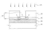
도 5를 참조하면, 통상의 얕은 트렌치 소자분리(Shallow Trench Isolation: 102)에 의해 액티브 영역(active area) 및 필드 영역(field area)이 구분되어 있는 반도체 기판(100)에 도전막(104), 베리어막(106) 및 측벽스페이서(108)로 구성되는 게이트 영역(110)이 형성되어 있다. 여기서, 상기 도전막(104)은 폴리실리콘 또는 폴리실리콘과 실리사이드막의 이중구조로 형성할 수 있다. 그리고, 상기 게이트 영역(110)과 트렌치 소자분리막(102) 사이에는 불순물(3B족의 B, 또는 5B족의 P, As) 이온주입에 의한 소오스/드레인 영역(112)이 형성되어 있다. 그리고, 상기 소오스/드레인 영역(112) 상부에는 콘택(116) 및 하부전극(118)이 형성되어 있다. Referring to FIG. 5, a
그리고, 상기 콘택(116) 및 하부전극(118)은 제1층간절연막(114)에 의해 둘러싸여 있으며, 상기 하부전극(118) 상부에는 산화막(120) 및 질화막(122)을 관통하는 콘택 플러그(124)가 형성되어 있다. 그리고, 상기 콘택 플러그(124) 상부에는 제2층간절연막(130)에 의해 둘러싸인 상변화 물질막(126) 및 상부전극(128)이 형성되어 있다. 그리고, 상기 상부전극(128)은 비아 콘택(132)을 통해 금속배선(134)과 연결되어 있다.The
여기서, 상기 하부전극(118)과 상변화 물질막(126)을 연결하는 콘택 플러그(124)는 본 발명에 따른 상변화 메모리 소자의 핵심구성으로서, 하부전극(118)에 접촉되는 바텀 영역에 비해 상변화 물질막(126)에 접촉되는 탑 영역의 면적이 상대적으로 크게(예컨대, 돛 형상, 바텀 영역에 비해 탑 영역의 단면이 보다 작은 원뿔 형상, 凸 형상) 형성되어 있다. 여기서, 상기 콘택 플러그(124)의 탑 영역은 높은 전류 밀도를 보장하여 구동시 전력 소모를 최소화할 수 있는 면적(약 50nm)을 가지도록 형성한다. 그리고, 상기 콘택 플러그(124)의 바텀 영역은 하부전극(118)과의 접촉 계면에서의 오믹 콘택 효과를 보다 향상시킬 수 있는 면적으로 형성한다.Here, the
그러면, 하기에서는 도 6a 내지 도 6h를 참조하여 본 발명에 따른 상변화 메모리 소자의 핵심 구성인 콘택 플러그 제조 과정을 순차적으로 살펴보기로 하자.Next, a process of manufacturing a contact plug, which is a core component of the phase change memory device according to the present invention, will be described sequentially with reference to FIGS. 6A to 6H.
먼저, 도 6a를 참조하면, 예컨대 B(붕소)와 같은 3B족 불순물이 도우핑되어 있는 p타입(또는 P, As와 같은 5B족 불순물이 도우핑되어 있는 n타입)의 반도체 기 판(200) 상부에 하부전극(202)을 형성한다. 여기서, 상기 하부전극(202)은, 예컨대 텅스텐막으로 형성할 수 있다.First, referring to FIG. 6A, a
계속해서, 상기 하부전극(202) 상부에 50~500Å 두께로 제1층간절연막(204)을 증착한다. 이때, 상기 제1층간절연막(204)은, 예컨대 SiO2, HTO(High Temperature Oxide), MTO(Middle Temperature Oxide), MTON2O(Middle Temperature Oxide Nitride Oxide), TEOS, USG, SOG, 또는 고밀도 플라즈마 산화막(HDP:High Density Plasma oxide)으로 형성할 수 있다. 이어서, 상기 제1층간절연막(204) 상부에 제2층간절연막(206)을 500~950Å 두께로 증착한다. 이때, 상기 제2층간절연막(206)은 상기 제1층간절연막(206)에 대하여 식각 선택비를 가지는 물질막으로서, 예컨대, Si3N4과 같은 질화막으로 형성하는 것이 바람직하다. 그리고, 상기 제1층간절연막(204) 및 제2층간절연막(206)은 압력, 온도, 인가되는 에너지 및 기압에 따라, 대기압 분위기하에서 이루어지는 APCVD(Atmospheric Pressure Chemical Vapor Deposition), 저압 분위기하에서 이루어지는 LPCVD(Low Pressure CVD), 플라즈마 분위기하에서 이루어지는 PECVD(Plasma Enhanced CVD) 공정을 통해 증착할 수 있다.Subsequently, a first
도 6b를 참조하면, 상기 제2층간절연막(206) 상부에, 상기 제2층간절연막(206)을 식각하기 위한 포토 마스크 패턴(208)을 형성한다. 여기서, 상기 포토 마스크 패턴(208)은, 상기 제2층간절연막(206) 상부에 포지티브 또는 네거티브 타입의 포토레지스트를 도포한 뒤, 노광 및 현상 공정을 실시하여 형성될 수 있다. 그 리고, 상기 인접한 포토 마스크 패턴(208) 사이의 개구(210)의 수평거리는, 구동시 전력 소모를 줄이기 위하여 50nm 이하로 형성한다. Referring to FIG. 6B, a
이어서, 상기 포토 마스크 패턴(208)을 자기정렬된 식각마스크로서 이용하여 상기 제2층간절연막(206)에 대하여 건식 식각 공정(212)을 실시한다. 이때, 상기 건식 식각 공정(212)은 예컨대, 가스 플라즈마, 이온빔, 또는 스퍼터링을 이용하여 실시할 수 있다. 이때, 가스 플라즈마를 이용할 경우, 프로세스 챔버 내부의 압력은 예컨대 35mT, RF 파워는 400W로 유지하는 것이 바람직하다. 그리고, CH2F2(20SCCM), O2(20SCCM) 및 Ar(180SCCM)을 프로세스 챔버 내부로 주입하여 약 57초간 식각 공정을 실시한다.Subsequently, a
도 6c를 참조하면, 상기 건식 식각 공정(212)에 대한 결과가 도시되어 있다. 상기 건식 식각 공정은(212) 이방성 식각 특성을 가진다. 따라서, 도 6c에 도시된 것과 같이, 상기 포토 마스크 패턴(208)의 개구(210)에 의해 노출된 제2층간절연막(206)이 하부로 수직 식각되어, 상기 제1층간절연막(202)을 노출시키는 제1콘택홀(214)이 형성된다. 이때, 상기 제1콘택홀(214)의 수평거리는, 상기 건식 식각 공정(212)시 식각 마스크로서 이용된 포토 마스크 패턴(208)의 개구(210) 수평거리에 따라 50nm 이하로 형성된다. Referring to FIG. 6C, the results for the
계속해서, 도 6d를 참조하면, 상기 제1콘택홀(214)이 형성되어 있는 반도체 기판(200)에 대하여 포토 마스크 패턴을 비롯한 식각 공정에 의한 공정 부산물(by-product)을 말끔히 제거하기 위한 에싱(ashing) 공정을 실시한다.6D, an ashing for neatly removing process by-products by an etching process including a photomask pattern with respect to the
계속해서, 상기 제1콘택홀(214)에 의해 노출된 상기 제1층간절연막(204)을 식각하기 위한 습식 식각 공정(216)을 실시한다. 상기 습식 식각 공정(216)시 프로세스 챔버 내부의 압력은 예컨대 40mT, RF 파워는 45W로 유지하는 것이 바람직하다. 그리고, CF4(80SCCM) 및 O2(20SCCM)을 식각 에천트로서 이용하여 약 30초간 식각 공정을 실시한다. 이러한 습식 식각 공정(216)은 등방성 식각 특징을 가진다. 따라서, 상기 습식 식각 공정(216)을 실시하게 되면, 상기 제1콘택홀(214)에 의해 노출된 제1층간절연막(참조부호 A) 영역뿐 아니라 제2층간절막(106) 하부(참조부호 B) 영역에 대해서도 식각이 진행된다.Subsequently, a
통상적으로, 습식 에천트가 사용되는 습식 식각 공정은 등방석 식각 공정이므로 식각타겟막의 가로길이 및 세로길이가 동일한 비율로 식각되는 특징이 있다. 그러므로, 상기 제1층간절연막(204)에 대하여 습식 식각 공정(216)을 실시하게 되면, 제1콘택홀(214)에 의해 노출된 영역(참조부호 A)이 식각되는 두께와 동일한 길이만큼 제2층간절연막(206) 하부(참조부호 B)로도 식각 공정이 진행된다. 즉, 상기 제1콘택홀(214)에 의해 노출된 제2층간절연막(206)의 에지영역으로 언더컷 식각이 진행된다. 그 결과, 상기 제1콘택홀(214) 하부로 상기 제1콘택홀(214)에 비해 보다 큰 수평거리를 가지는 제2콘택홀(218)이 형성된다. 그리고, 이처럼 형성된 제1콘택홀(214) 및 제2콘택홀(218)은 전체적으로 콘택 플러그홀(220)을 이루게 된다. 그리고 상기 콘택 플러그홀(220) 내부에는 후속의 공정을 통해 도전물이 필링됨으로써, 하부전극(202)과 상변화 물질막(도시되지 않음)을 서로 전기적으로 연결하는 콘택 플러그, 즉 상변화 물질막에 전류를 인가해주는 노드로서 기능하는 콘택 플러그가 형성된다.Typically, since the wet etching process using the wet etchant is an isotropic etching process, the horizontal and vertical lengths of the etching target layer are etched at the same ratio. Therefore, when the
도 6e에는 상기 콘택 플러그홀(220) 내부에 도전물을 필링하는 과정이 도시되어 있다. 도 6e를 참조하면, 먼저, 상기 제1콘택홀(214)을 형성하기 위한 건식 식각 공정(212) 및 제2콘택홀(218)을 형성하기 위한 습식 식각 공정(216)을 실시하는 과정에서 데미지를 입은 하부전극(202) 표면을 제거하기 위한 등방성 식각 공정을 실시한다. 이러한 등방성 식각 공정은 하부전극(202) 표면의 데미지층을 제거하기 위한 추가적인 공정이다. 그러나, 하부전극(202)이 텅스텐일 경우에는 데미지층 제거를 위한 등방성 식각 공정은 필수적으로 실시하는 것이 바람직하며, 이때 식각 에천트로서는 CF4, NF3 및 O2가 사용될 수 있다. 그리고, 도면상으로 표현하지는 않았으나, 상기와 같은 등방성 식각 공정을 실시하면, 하부전극(202) 표면의 소정 두께가 등방성 식각되어 오목한 형상을 나타낸다.6E illustrates a process of filling a conductive material in the
이어서, 상기와 같은 등방성 식각 공정을 실시하여 하부전극(202) 표면의 데미지층을 제거한 뒤, 상기 반도체 기판(200) 전면 상부에 도전물(222)을 증착한다. 그 결과, 상기 콘택 플러그홀(220) 내부에 도전물이 필링된다. 이때, 상기 도전물(222)로서는, 도핑된 폴리실리콘, 텅스텐, 알루미늄, 탄탈륨 또는 구리가 이용될 수 있다.Subsequently, the damage layer on the surface of the
도 6f를 참조하면, 상기 도전물(222)이 증착되어 있는 반도체 기판(200)에 대하여, 에치백(etch back) 또는 화학적 기계 연마(CMP:Chemical Mechanical Polishing) 공정등과 같은 표면 평탄화 공정을 실시한다. 그 결과, 상기 제2층간절연막(206) 상부의 도전물은 모두 제거되고, 콘택 플러그홀(220) 내부에만 도전물이 존재하게 되어 凸 형상(또는 돛 형상, 바텀 영역에 비해 탑 영역의 단면이 보다 작은 원뿔 형상) 의 콘택 플러그(224)가 형성된다. Referring to FIG. 6F, a surface planarization process, such as an etch back or chemical mechanical polishing (CMP) process, is performed on the
상기 도 6f에 도시된 것과 같이, 탑 영역의 수평거리(C)에 비해 바텀 영역의 수평거리(D)가 상대적으로 넓은 凸 형상의 콘택 플러그(224)는 본 발명의 상변화 메모리 소자에 있어서의 핵심 구성이다. 따라서, 본 발명에서는 상기 콘택 플러그(224)의 탑 영역의 수평거리(C)는 약 50nm로 형성하였다. 그리고, 상기 콘택 플러그(224)의 바텀 영역의 수평거리(D)는 제1층간절연막(204)의 증착두께에 따라 달라지게 된다. 즉, "1nm=10Å" 이라는 관계식에 의하여, 제1층간절연막(204)을 10Å 두께로 형성하였을 경우에는 콘택 플러그(224)의 바텀 영역의 수평거리(D)는 52nm가 된다(좌우 양측으로 각각 1nm씩 증가되므로). 따라서, 본 발명에서와 같이 상기 제1층간절연막(204)을 50~500Å 두께로 증착할 경우, 상기 콘택 플러그(224)의 바텀 영역의 수평거리(D)는 60~150nm로 탄력적으로 변화될 수 있다. 즉, 상기 바텀 영역의 수평거리(D)는 탑 영역의 수평거리(C)에 비해 "제1층간절연막의 두께×2" 에 해당되는 길이만큼 보다 크게 형성되어진다.As shown in FIG. 6F, the 플러그 -shaped
상변화 메모리 소자를 구현함에 있어서, 상변화 물질막과 콘택 플러그간의 접촉 면적은 작고, 하부전극과 콘택 플러그간의 접촉 면적은 넓을수록 상변화 메모리 소자의 전기적 특성이 우수해진다. 즉, 콘택 플러그를 통해 상변화 물질막에 전류를 인가할 시에는 상변화 물질막과 콘택 플러그간의 접촉 계면이 작아야 상변화 물질막측으로 인가되는 전류 밀도를 증가시켜 구동시 전력 소모를 최소화할 수 있게 된다.In implementing the phase change memory device, the smaller the contact area between the phase change material film and the contact plug and the larger the contact area between the lower electrode and the contact plug, the better the electrical characteristics of the phase change memory device. That is, when current is applied to the phase change material film through the contact plug, the contact interface between the phase change material film and the contact plug must be small to increase the current density applied to the phase change material film side to minimize power consumption during driving. do.
한편, 상기 콘택 플러그와 하부전극은 오믹 접촉(저항성 접촉)을 이루고 있는데, 콘택 플러그와 하부전극간의 접촉 계면이 협소할수록 접촉 저항을 제어하는 것이 어려워진다. 따라서, 본 발명에서와 같이, 콘택 플러그의 탑 영역에 비하여 바텀 영역의 수평거리를 상대적으로 크게 형성함으로써, 콘택 플러그와 하부전극간의 접촉 계면을 증가시켜 접촉 저항을 보다 용이하게 제어할 수 있도록 한다(오믹 콘택 효과 향상). 그 결과, 전체 상변화 메모리 소자의 리세트 및 세트 동작 특성을 향상시킬 수 있게 된다.On the other hand, the contact plug and the lower electrode is in ohmic contact (resistive contact), the narrower the contact interface between the contact plug and the lower electrode becomes difficult to control the contact resistance. Therefore, as in the present invention, the horizontal distance of the bottom region is made relatively larger than the top region of the contact plug, thereby increasing the contact interface between the contact plug and the lower electrode so that the contact resistance can be more easily controlled ( Improved ohmic contact effects). As a result, the reset and set operating characteristics of the entire phase change memory element can be improved.
이어서, 도 6g를 참조하면, 상기 콘택 플러그(224)가 형성되어 있는 반도체 기판(200) 전면 상부에 상변화 물질막(226)을 증착한다. 이러한 상변화 물질막(226)은 상변화 메모리 소자가 독창적인 특성을 나타내도록 하는 주요 구성 요소로서, Ge, Sb, Te, Se, Bi, Pb, Sn, As, S, Si, P, O 및 이들의 혼합물 또는 합금으로 구성되는 물질군에서 선택되는 물질중의 어느 하나로 형성할 수 있다. 보다 구체적으로, 게르마늄(Ge), 비스티윰(Sb) 및 텔루리윰(Te)으로 조성된 켈코겐 화합물(GST 또는 Ge-Sb-Te)이 대표적으로 사용될 수 있다. 또한, 상기한 GST 이외에 사용될 수 있는 켈코겐 화합물로는, As-Sb-Te, As-Gb-Te, As-Gb-Sb-Te, Sn-Sn-Te, In-Sn-Sn-Te, Ag-In-Sb-Te, 5A족 원소(Ta, Nb, V)-Sb-Te, 5A족 원소(Ta, Nb, V)-Sb-Se, 6A족 원소(W, Mo, Cr)-Sb-Te, 6A족 원소(W, Mo, Cr)-Sb-Se 등이 사용될 수 있다. 또한, 상기 화합물에 질소를 더 포함시켜 사용하는 것도 가능하다. 그리고, 이 러한 상변화 물질막(226)은, 예컨대 100℃~300℃의 온도하에서 약 100Å~1000Å 두께로 형성하는 것이 바람직하다.Next, referring to FIG. 6G, a phase
이어서, 상기 상변화 물질막(226) 상부에 상부전극용 도전막(228)을 증착한다. 이러한 도전막(228)으로서는, 질소를 포함하는 도전성 물질, 금속, 금속과 금속 실리사이드의 이중막, 합금, 금속 산화질화물 또는 도전성 탄소화합물로 형성할 수 있다. 보다 구체적으로, TiN, TaN, WN, MoN, NbN, TiSiN, TiAlN, TiBN, ZrSiN, WSiN, WBN, ZrAlN, MoSiN, MoAlN, TaSiN, TaAlN등과 같이 질소 원소를 포함하는 도전성 물질, 또는 Ti, W, Mo, Ta, TiSi, TaSi, TiW, TiON, TiAlON, WON, TaON 등으로 이루어진 그룹에서 선택된 어느 하나 또는 이들의 조합으로 이루어진 도전성 물질막으로 형성할 수 있다.Subsequently, an upper electrode
이어서, 상기 도전막(228) 상부에 SiO2, HTO, MTO, MTON2O, TEOS, USG, SOG, 또는 HDP등의 산화막(230)을 증착한다.Subsequently, an
도 6h를 참조하면, 통상의 사진식각 공정을 실시하여 상기 산화막 패턴(230a)을 형성한다. 그리고, 상기 산화막 패턴(230a)을 식각 마스크로서 이용하여 하부의 도전막(228) 및 상변화 물질막(226)을 식각한다.Referring to FIG. 6H, the
그 결과, 상기 플러그 패턴(224) 상부에는 상변화 물질막(226a) 및 하부전극(228a)이 형성된다. 이어서, 도면상으로 도시하지는 않았으나, 상기 결과물에 캡핑층, 비트라인과의 연결을 위한 비아 콘택을 형성하고, 메탈 공정을 진행함으로써, 상변화 메모리 소자를 완성하게 된다.As a result, a phase
이상, 도 6a 내지 도 6h를 참조하여, 본 발명의 바람직한 실시예에 따른 상변화 메모리 소자의 제조방법을 살펴보았다.6A to 6H, the method of manufacturing the phase change memory device according to the preferred embodiment of the present invention has been described.
종래에는 구동시의 전력 소모를 줄이기 위하여 상변화 물질막과 콘택 플러그간의 접촉 면적을 축소시켰다. 그로 인해, 상변화 물질막측으로 인가되는 전류 밀도를 높여 구동시의 전력 소모를 줄일 수 있는 효과는 얻을 수 있었다. 그러나, 콘택 플러그 사이즈가 줄어듦에 따라 하부전극과 콘택 플러그간의 접촉 면적 또한 감소되어 하부전극과 콘택 플러그간의 접촉 저항을 정밀하게 제어하기 어려워져 상변화 메모리 소자의 리세트 및 세트 동작 특성이 저하되는 문제점이 있었다.Conventionally, the contact area between the phase change material film and the contact plug is reduced in order to reduce power consumption during driving. Therefore, the effect of reducing the power consumption during driving by increasing the current density applied to the phase change material film side was obtained. However, as the contact plug size decreases, the contact area between the lower electrode and the contact plug is also reduced, making it difficult to precisely control the contact resistance between the lower electrode and the contact plug, thereby reducing the reset and set operation characteristics of the phase change memory device. There was this.
따라서, 본 발명에서는 상기와 같은 종래의 문제점을 해소하고자, 상변화 물질막(226a)과의 접촉 면적에 비해 하부전극(202)과의 접촉 면적을 상대적으로 크게 형성한 凸 형상의 콘택 플러그(224)를 구현하게 된 것이다. 즉, 상기 상변화 물질막(226a)과 접촉되는 콘택 플러그의 탑 영역(C)은 높은 전류 밀도가 유지되어 구동시 전력 소모를 최소화할 수 있는 면적(약 50nm)을 가지도록 형성한다. 그리고, 상기 하부전극(202)과 접촉되는 바텀 영역(D)은 공정 오류(콘택 플러그 형성을 위한 도전막 필링시 보이드가 발생되는 문제점)를 유발시키지 않는 범위내에서 콘택 플러그(224)와 하부전극(202)간의 오믹 콘택 효과를 보다 향상시킬 수 있는 면적으로 형성한다. 그 결과, 상변화 물질막(226a)과의 접촉 계면에 대해서는 높은 전류 밀도가 유지되어 구동시 전력 소모를 최소화할 수 있게 된다. 그리고, 하부전극(202)과의 접촉 계면에 대해서는 오믹 콘택 효과가 증대되어 상변화 메모리 소자의 리세트 및 세트 동작 특성이 보다 우수해진다(I=1/R, R=1/A).Accordingly, in the present invention, in order to solve the above-described problems, the
또한, 콘택 플러그를 형성함에 있어서, 직선측벽을 가지는 원통구조로 형성할 경우, 후속 공정 진행을 진행하거나 외부에서 가해지는 물리적인 힘에 의하여 콘택 플러그를 이루고 있는 도전물이 들뜨거나 이탈되는 경우가 있다. 그러나, 본 발명에서와 같이, 탑 영역에 비해 바텀 영역의 면적이 보다 큰 凸 형상으로 콘택 플러그(224)를 형성할 경우, 콘택 플러그(224)를 구성하는 도전물질이 층간절연막(204,206) 사이에 단단히 고정되어 들뜸 또는 이탈이 방지되는 부가적인 효과를 기대할 수 있게 된다.In addition, in forming the contact plug, when forming a cylindrical structure having a straight side wall, the conductive material constituting the contact plug may be lifted or released due to the progress of the subsequent process or by a physical force applied from the outside. . However, as in the present invention, when the
한편, 도 7a 내지 도 7c에는 본 발명의 또 다른 실시예에 따른 상변화 메모리 소자의 제조방법을 순차적으로 나타내는 단면도들이다.7A to 7C are cross-sectional views sequentially illustrating a method of manufacturing a phase change memory device according to still another embodiment of the present invention.
상기 도 6a 내지 도 6h를 통해 설명된 상변화 메모리 소자와 비교할 때, 도 7a 내지 도 7c을 통해 설명되어질 상변화 메모리 소자는 플러그 콘택의 구조 및 그 제조방법이 서로 다르다. 따라서, 플러그 콘택 이외의 타 구성 요소에 대해서는 상기 도 6a 내지 도 6h를 참조하여 설명된다.Compared with the phase change memory device described with reference to FIGS. 6A through 6H, the structure of the plug contact and the manufacturing method thereof differ from those described with reference to FIGS. 7A through 7C. Therefore, other components other than the plug contact will be described with reference to FIGS. 6A to 6H.
먼저, 도 7a를 참조하면, 예컨대 B(붕소)와 같은 3B족 불순물이 도우핑되어 있는 p타입(또는 P, As와 같은 5B족 불순물이 도우핑되어 있는 n타입)의 반도체 기판(300) 상부에 하부전극(302)을 형성한다. 여기서, 상기 하부전극(302)은, 예컨대 텅스텐막으로 형성할 수 있다.First, referring to FIG. 7A, an upper portion of a
계속해서, 상기 하부전극(302) 상부에 약 1000Å 두께로 층간절연막(304)을 증착한다. 이때, 상기 층간절연막(304)은, 예컨대 SiO2, HTO(High Temperature Oxide), MTO(Middle Temperature Oxide), MTON2O(Middle Temperature Oxide Nitride Oxide), TEOS, USG, SOG, 고밀도 플라즈마 산화막(HDP:High Density Plasma oxide) 또는 Si3N4과 같은 질화막으로 형성할 수 있다. 그리고, 상기 층간절연막(304)은 압력, 온도, 인가되는 에너지 및 기압에 따라, 대기압 분위기하에서 이루어지는 APCVD(Atmospheric Pressure Chemical Vapor Deposition), 저압 분위기하에서 이루어지는 LPCVD(Low Pressure CVD), 플라즈마 분위기하에서 이루어지는 PECVD(Plasma Enhanced CVD) 공정을 통해 증착할 수 있다.Subsequently, an
도 7b를 참조하면, 상기 층간절연막(304) 상부에 포토 마스크 패턴(306)을 형성한다. 이때, 상기 포토 마스크 패턴(306)의 개구(308)는 수평거리는 최종적으로 형성되어질 콘택 플러그의 탑 영역 수평 거리에 비해 보다 좁게 형성하는 것이 바람직하다. 즉, 구동시 소비 전력 감소를 위하여, 콘택 플러그의 탑 영역의 수평 거리를 50nm로 설정할 경우, 상기 포토 마스크 패턴(306)의 개구(308)는 50nm 보다 작은 수평 거리를 유지하도록 형성한다.Referring to FIG. 7B, a
따라서, 상기 포토 마스크 패턴(306)을 자기정렬된 식각마스크로서 이용하여 상기 층간절연막(304)에 대하여 습식 식각 공정(310)을 실시한다. 그 결과, 상기 층간절연막(304)을 관통하며, 상기 하부전극(302)의 상부 표면을 노출시키는 플러그 콘택홀(312)이 형성된다. 이때, 상기 습식 식각 공정(310)은 등방성 식각 특징을 가진다. 따라서, 상기 플러그 콘택홀(312)의 측벽 프로파일은 도 7b에 도시된 것과 같이 곡선형을 나타낼 수 있다. 그리고, 상기 포토 마스크 패턴(306)으로 인 해 상기 습식 식각 공정(310) 초반에 층간절연막(304)에 대한 식각이 저지됨으로 인해, 상기 플러그 콘택홀(312)의 탑 영역은 바텀 영역에 비해 수평거리가 보다 작게 형성된다.Accordingly, the
도 7c를 참조하면, 상기 포토 마스크 패턴(306)을 제거한 뒤, 상기 플러그 콘택홀(312) 내부에 도전물을 필링하여 플러그 콘택(314)을 형성한다. 상기 플러그 콘택홀(312) 내부에 필링되는 도전물로서는, 도핑된 폴리실리콘, 텅스텐, 알루미늄, 탄탈륨 또는 구리가 이용될 수 있다.Referring to FIG. 7C, after removing the
이어서, 상기 플러그 콘택(314) 상부에 상변화 물질막(316), 상부전극(318) 및 산화막(320)을 차례로 증착한다. 여기서, 상기 상변화 물질막(316)은 Ge, Sb, Te, Se, Bi, Pb, Sn, As, S, Si, P, O 및 이들의 혼합물 또는 합금으로 구성되는 물질군에서 선택되는 물질중의 어느 하나로 형성할 수 있다. 보다 구체적으로, 게르마늄(Ge), 비스티윰(Sb) 및 텔루리윰(Te)으로 조성된 켈코겐 화합물(GST 또는 Ge-Sb-Te)이 대표적으로 사용될 수 있다. 또한, 상기한 GST 이외에 사용될 수 있는 켈코겐 화합물로는, As-Sb-Te, As-Gb-Te, As-Gb-Sb-Te, Sn-Sn-Te, In-Sn-Sn-Te, Ag-In-Sb-Te, 5A족 원소(Ta, Nb, V)-Sb-Te, 5A족 원소(Ta, Nb, V)-Sb-Se, 6A족 원소(W, Mo, Cr)-Sb-Te, 6A족 원소(W, Mo, Cr)-Sb-Se 등이 사용될 수 있다. 또한, 상기 화합물에 질소를 더 포함시켜 사용하는 것도 가능하다. 그리고, 상부전극(318)은 질소를 포함하는 도전성 물질, 금속, 금속과 금속 실리사이드의 이중막, 합금, 금속 산화질화물 또는 도전성 탄소화합물로 형성할 수 있다. 보다 구체적으로, TiN, TaN, WN, MoN, NbN, TiSiN, TiAlN, TiBN, ZrSiN, WSiN, WBN, ZrAlN, MoSiN, MoAlN, TaSiN, TaAlN등과 같이 질소 원소를 포함하는 도전성 물질, 또는 Ti, W, Mo, Ta, TiSi, TaSi, TiW, TiON, TiAlON, WON, TaON 등으로 이루어진 그룹에서 선택된 어느 하나 또는 이들의 조합으로 이루어진 도전성 물질막으로 형성할 수 있다. 그리고, 상기 산화막(320)은 SiO2, HTO, MTO, MTON2O, TEOS, USG, SOG, 또는 HDP등의 산화막으로 형성할 수 있다.Subsequently, a phase
이어서, 도면상에 도시하지는 않았지만, 상기 결과물에 캡핑층, 비트라인과의 연결을 위한 비아 콘택을 형성하고, 메탈 공정을 진행함으로써, 상변화 메모리 소자를 완성하게 된다.Subsequently, although not shown in the figure, a via contact for connecting the capping layer and the bit line is formed on the resultant, and a metal process is performed to complete the phase change memory device.
이와 같이, 상기 플러그 콘택(314)을 형성함에 있어서, 탑 영역의 수평거리(E)에 비해 바텀 영역(F)의 수평거리가 상대적으로 넓게 형성함으로 인해 상변화 메모리 소자의 전기적 특성이 향상된다. 즉, 상기 상변화 물질막(316)에 전류를 인가할 시에는 상기 플러그 콘택(314)의 탑 영역과 상변화 물질막(316)간의 접촉 계면(50nm 이하)이 작아 구동시 전력 소모를 줄일 수 있게 된다. 그리고, 상기 콘택 플러그(314)의 바텀 영역과 하부전극(302)간의 접촉 계면(50nm 이상)에서는 오믹 접촉(저항성 접촉) 특성이 향상되어 결과적으로 전체 상변화 메모리 소자의 리세트 및 세트 동작 특성이 우수해지는 효과를 얻을 수 있게 된다. As described above, in forming the
상기한 바와 같이 본 발명에서는, 상변화 물질막으로 전류를 공급하는 콘택 플러그를 형성함에 있어서, 상변화 물질막과 접하는 탑 영역에 비해 하부전극과 접하는 바텀 영역의 면적을 보다 크게 형성한다. 그 결과, 상변화 물질막에 대해서는 높은 전류 밀도가 보장되어 구동시 전력 소모를 최소화할 수 있게 된다. 그리고, 하부전극과의 접촉 계면은 증가되어 오믹 콘택 효과가 향상됨으로써, 상변화 메모리 소자의 리세트 및 세트 동작 특성이 우수해지는 효과를 얻을 수 있게 된다.As described above, in the present invention, in forming the contact plug for supplying current to the phase change material film, the area of the bottom area in contact with the lower electrode is larger than the top area in contact with the phase change material film. As a result, high current density is ensured for the phase change material film, thereby minimizing power consumption during driving. In addition, the contact interface with the lower electrode is increased to improve the ohmic contact effect, thereby obtaining an effect of excellent reset and set operation characteristics of the phase change memory device.
또한, 탑 영역에 비해 바텀 영역의 면적이 보다 넓은 상기 콘택 플러그의 구조적 특징으로 인해 후속의 공정 또는 외부의 물리적인 힘에 의해 콘택 플러그를 구성하는 도전물이 들뜨거나 이탈되는 문제점이 방지되는 부가적인 효과를 얻을 수 있게 된다.In addition, due to the structural feature of the contact plug having a larger area of the bottom area than the top area, an additional problem is prevented that the conductive material constituting the contact plug is lifted or released by a subsequent process or external physical force. You will get the effect.
Claims (20)
Priority Applications (3)
| Application Number | Priority Date | Filing Date | Title |
|---|---|---|---|
| KR1020050128477A KR100655082B1 (en) | 2005-12-23 | 2005-12-23 | Phase change memory device and manufacturing method thereof |
| TW095143634A TW200737502A (en) | 2005-12-23 | 2006-11-24 | Phase-change memory device and methods of fabricating the same |
| US11/643,702 US20070210348A1 (en) | 2005-12-23 | 2006-12-22 | Phase-change memory device and methods of fabricating the same |
Applications Claiming Priority (1)
| Application Number | Priority Date | Filing Date | Title |
|---|---|---|---|
| KR1020050128477A KR100655082B1 (en) | 2005-12-23 | 2005-12-23 | Phase change memory device and manufacturing method thereof |
Publications (1)
| Publication Number | Publication Date |
|---|---|
| KR100655082B1 true KR100655082B1 (en) | 2006-12-08 |
Family
ID=37732472
Family Applications (1)
| Application Number | Title | Priority Date | Filing Date |
|---|---|---|---|
| KR1020050128477A Expired - Fee Related KR100655082B1 (en) | 2005-12-23 | 2005-12-23 | Phase change memory device and manufacturing method thereof |
Country Status (3)
| Country | Link |
|---|---|
| US (1) | US20070210348A1 (en) |
| KR (1) | KR100655082B1 (en) |
| TW (1) | TW200737502A (en) |
Cited By (10)
| Publication number | Priority date | Publication date | Assignee | Title |
|---|---|---|---|---|
| KR100825767B1 (en) * | 2006-12-05 | 2008-04-29 | 한국전자통신연구원 | Phase change memory device and manufacturing method thereof |
| KR100935591B1 (en) * | 2007-12-26 | 2010-01-07 | 주식회사 하이닉스반도체 | Phase change memory device capable of improving contact resistance and reset current and manufacturing method thereof |
| US7767994B2 (en) | 2006-12-05 | 2010-08-03 | Electronics And Telecommunications Research Institute | Phase-change random access memory device and method of manufacturing the same |
| US7772101B2 (en) | 2007-08-10 | 2010-08-10 | Hynix Semiconductor Inc. | Phase-change memory device and method for manufacturing the same |
| US7777214B2 (en) | 2008-01-25 | 2010-08-17 | Samsung Electronics Co., Ltd. | Phase change memory device with a novel electrode |
| KR100985757B1 (en) * | 2008-05-26 | 2010-10-06 | 주식회사 하이닉스반도체 | A method of manufacturing a phase change memory device having a lower electrode contact layer |
| US7939366B2 (en) | 2007-07-25 | 2011-05-10 | Samsung Electronics Co., Ltd. | Phase change memory devices and methods of forming the same |
| KR101124340B1 (en) * | 2010-12-13 | 2012-03-16 | 주식회사 하이닉스반도체 | Phase-Change Memory Device and Fabrication Method Thereof |
| KR20120054885A (en) * | 2010-11-22 | 2012-05-31 | 삼성전자주식회사 | Non-volatile memory device having bottom electrode |
| KR101548241B1 (en) | 2013-12-31 | 2015-08-28 | (재)한국나노기술원 | manufacturing method of semiconductor devices with trench and semiconductor devices thereby |
Families Citing this family (37)
| Publication number | Priority date | Publication date | Assignee | Title |
|---|---|---|---|---|
| KR100679270B1 (en) * | 2006-01-27 | 2007-02-06 | 삼성전자주식회사 | Phase change memory device and manufacturing method thereof |
| US7772120B2 (en) * | 2007-01-09 | 2010-08-10 | International Business Machines Corporation | Chemical vapor deposition method for the incorporation of nitrogen into materials including germanium and antimony |
| TWI333273B (en) * | 2007-05-02 | 2010-11-11 | Powerchip Technology Corp | Methods for reducing a contact area between heating electrode and phase-change material layer, phase-change memory devices and methods for fabricating the same |
| TW200913249A (en) * | 2007-09-04 | 2009-03-16 | Ind Tech Res Inst | Phase-change memory and fabrication method thereof |
| JP5063337B2 (en) * | 2007-12-27 | 2012-10-31 | 株式会社日立製作所 | Semiconductor device |
| US7768812B2 (en) | 2008-01-15 | 2010-08-03 | Micron Technology, Inc. | Memory cells, memory cell programming methods, memory cell reading methods, memory cell operating methods, and memory devices |
| US8378328B2 (en) * | 2008-02-22 | 2013-02-19 | International Business Machines Corporation | Phase change memory random access device using single-element phase change material |
| US7855435B2 (en) * | 2008-03-12 | 2010-12-21 | Qimonda Ag | Integrated circuit, method of manufacturing an integrated circuit, and memory module |
| US7579210B1 (en) * | 2008-03-25 | 2009-08-25 | Ovonyx, Inc. | Planar segmented contact |
| US8034655B2 (en) | 2008-04-08 | 2011-10-11 | Micron Technology, Inc. | Non-volatile resistive oxide memory cells, non-volatile resistive oxide memory arrays, and methods of forming non-volatile resistive oxide memory cells and memory arrays |
| US8211743B2 (en) | 2008-05-02 | 2012-07-03 | Micron Technology, Inc. | Methods of forming non-volatile memory cells having multi-resistive state material between conductive electrodes |
| US7786463B2 (en) * | 2008-05-20 | 2010-08-31 | Seagate Technology Llc | Non-volatile multi-bit memory with programmable capacitance |
| US8134137B2 (en) | 2008-06-18 | 2012-03-13 | Micron Technology, Inc. | Memory device constructions, memory cell forming methods, and semiconductor construction forming methods |
| US9343665B2 (en) | 2008-07-02 | 2016-05-17 | Micron Technology, Inc. | Methods of forming a non-volatile resistive oxide memory cell and methods of forming a non-volatile resistive oxide memory array |
| US8411477B2 (en) | 2010-04-22 | 2013-04-02 | Micron Technology, Inc. | Arrays of vertically stacked tiers of non-volatile cross point memory cells, methods of forming arrays of vertically stacked tiers of non-volatile cross point memory cells, and methods of reading a data value stored by an array of vertically stacked tiers of non-volatile cross point memory cells |
| US8427859B2 (en) | 2010-04-22 | 2013-04-23 | Micron Technology, Inc. | Arrays of vertically stacked tiers of non-volatile cross point memory cells, methods of forming arrays of vertically stacked tiers of non-volatile cross point memory cells, and methods of reading a data value stored by an array of vertically stacked tiers of non-volatile cross point memory cells |
| US8289763B2 (en) | 2010-06-07 | 2012-10-16 | Micron Technology, Inc. | Memory arrays |
| US8351242B2 (en) | 2010-09-29 | 2013-01-08 | Micron Technology, Inc. | Electronic devices, memory devices and memory arrays |
| US8759809B2 (en) | 2010-10-21 | 2014-06-24 | Micron Technology, Inc. | Integrated circuitry comprising nonvolatile memory cells having platelike electrode and ion conductive material layer |
| US8796661B2 (en) | 2010-11-01 | 2014-08-05 | Micron Technology, Inc. | Nonvolatile memory cells and methods of forming nonvolatile memory cell |
| US8526213B2 (en) | 2010-11-01 | 2013-09-03 | Micron Technology, Inc. | Memory cells, methods of programming memory cells, and methods of forming memory cells |
| US9454997B2 (en) | 2010-12-02 | 2016-09-27 | Micron Technology, Inc. | Array of nonvolatile memory cells having at least five memory cells per unit cell, having a plurality of the unit cells which individually comprise three elevational regions of programmable material, and/or having a continuous volume having a combination of a plurality of vertically oriented memory cells and a plurality of horizontally oriented memory cells; array of vertically stacked tiers of nonvolatile memory cells |
| US8431458B2 (en) | 2010-12-27 | 2013-04-30 | Micron Technology, Inc. | Methods of forming a nonvolatile memory cell and methods of forming an array of nonvolatile memory cells |
| US8791447B2 (en) | 2011-01-20 | 2014-07-29 | Micron Technology, Inc. | Arrays of nonvolatile memory cells and methods of forming arrays of nonvolatile memory cells |
| US8488365B2 (en) | 2011-02-24 | 2013-07-16 | Micron Technology, Inc. | Memory cells |
| KR20120104031A (en) * | 2011-03-11 | 2012-09-20 | 삼성전자주식회사 | Phase change material layer, method of forming a phase change layer, phase change memory device and method of manufacturing a phase change memory device |
| US8537592B2 (en) | 2011-04-15 | 2013-09-17 | Micron Technology, Inc. | Arrays of nonvolatile memory cells and methods of forming arrays of nonvolatile memory cells |
| TWI549229B (en) * | 2014-01-24 | 2016-09-11 | 旺宏電子股份有限公司 | Multiple phase change materials in a memory device for system on a chip application |
| KR102307633B1 (en) * | 2014-12-10 | 2021-10-06 | 삼성전자주식회사 | Semiconductor device and method for manufacturing the same |
| US10634938B2 (en) * | 2017-03-30 | 2020-04-28 | Massachusetts Institute Of Technology | GSST and applications in optical devices |
| KR102421766B1 (en) * | 2017-07-07 | 2022-07-18 | 삼성전자주식회사 | Three-dimensional semiconductor device and method for fabricating the same |
| WO2019152593A1 (en) | 2018-01-31 | 2019-08-08 | Massachusetts Institute Of Technology | Methods and apparatus for modulating light with phase-change materials |
| CN111640746A (en) * | 2019-09-17 | 2020-09-08 | 福建省晋华集成电路有限公司 | Semiconductor device, forming method thereof and memory |
| US11558957B2 (en) * | 2020-06-12 | 2023-01-17 | Raytheon Company | Shape memory thermal capacitor and methods for same |
| CN117693284A (en) * | 2022-08-25 | 2024-03-12 | 华为技术有限公司 | Gate tube materials, phase change memory chips, storage devices and electronic equipment |
| US12114583B1 (en) | 2023-08-01 | 2024-10-08 | Huazhong University Of Science And Technology | Se-based selector material, selector unit and method for preparing the same |
| CN117156957A (en) * | 2023-08-01 | 2023-12-01 | 华中科技大学 | Se-based gate tube material, gate tube unit and preparation method of Se-based gate tube material |
Family Cites Families (11)
| Publication number | Priority date | Publication date | Assignee | Title |
|---|---|---|---|---|
| JP2001077232A (en) * | 1999-09-06 | 2001-03-23 | Mitsubishi Electric Corp | Semiconductor device and method of manufacturing the same |
| US6534781B2 (en) * | 2000-12-26 | 2003-03-18 | Ovonyx, Inc. | Phase-change memory bipolar array utilizing a single shallow trench isolation for creating an individual active area region for two memory array elements and one bipolar base contact |
| US6946840B1 (en) * | 2001-03-08 | 2005-09-20 | General Electric Company | Integrated and independently controlled transmit only and receive only coil arrays for magnetic resonance systems |
| US6586761B2 (en) * | 2001-09-07 | 2003-07-01 | Intel Corporation | Phase change material memory device |
| US6861267B2 (en) * | 2001-09-17 | 2005-03-01 | Intel Corporation | Reducing shunts in memories with phase-change material |
| KR100413828B1 (en) * | 2001-12-13 | 2004-01-03 | 삼성전자주식회사 | Semiconductor device and method of making the same |
| US6891747B2 (en) * | 2002-02-20 | 2005-05-10 | Stmicroelectronics S.R.L. | Phase change memory cell and manufacturing method thereof using minitrenches |
| KR100505658B1 (en) * | 2002-12-11 | 2005-08-03 | 삼성전자주식회사 | Semiconductor device having MIM capacitor |
| WO2004057618A2 (en) * | 2002-12-19 | 2004-07-08 | Koninklijke Philips Electronics N.V. | Electric device comprising a layer of phase change material and method of manufacturing the same |
| US7776744B2 (en) * | 2005-09-01 | 2010-08-17 | Micron Technology, Inc. | Pitch multiplication spacers and methods of forming the same |
| US20070099328A1 (en) * | 2005-10-31 | 2007-05-03 | Yuan-Sheng Chiang | Semiconductor device and interconnect structure and their respective fabricating methods |
-
2005
- 2005-12-23 KR KR1020050128477A patent/KR100655082B1/en not_active Expired - Fee Related
-
2006
- 2006-11-24 TW TW095143634A patent/TW200737502A/en unknown
- 2006-12-22 US US11/643,702 patent/US20070210348A1/en not_active Abandoned
Cited By (13)
| Publication number | Priority date | Publication date | Assignee | Title |
|---|---|---|---|---|
| KR100825767B1 (en) * | 2006-12-05 | 2008-04-29 | 한국전자통신연구원 | Phase change memory device and manufacturing method thereof |
| US7767994B2 (en) | 2006-12-05 | 2010-08-03 | Electronics And Telecommunications Research Institute | Phase-change random access memory device and method of manufacturing the same |
| US7939366B2 (en) | 2007-07-25 | 2011-05-10 | Samsung Electronics Co., Ltd. | Phase change memory devices and methods of forming the same |
| KR101019984B1 (en) * | 2007-08-10 | 2011-03-09 | 주식회사 하이닉스반도체 | Phase change memory device and manufacturing method thereof |
| US7772101B2 (en) | 2007-08-10 | 2010-08-10 | Hynix Semiconductor Inc. | Phase-change memory device and method for manufacturing the same |
| KR100935591B1 (en) * | 2007-12-26 | 2010-01-07 | 주식회사 하이닉스반도체 | Phase change memory device capable of improving contact resistance and reset current and manufacturing method thereof |
| US7964498B2 (en) | 2007-12-26 | 2011-06-21 | Hynix Semiconductor Inc. | Phase-change memory device capable of improving contact resistance and reset current and method of manufacturing the same |
| US7777214B2 (en) | 2008-01-25 | 2010-08-17 | Samsung Electronics Co., Ltd. | Phase change memory device with a novel electrode |
| KR100985757B1 (en) * | 2008-05-26 | 2010-10-06 | 주식회사 하이닉스반도체 | A method of manufacturing a phase change memory device having a lower electrode contact layer |
| KR20120054885A (en) * | 2010-11-22 | 2012-05-31 | 삼성전자주식회사 | Non-volatile memory device having bottom electrode |
| KR101685022B1 (en) | 2010-11-22 | 2016-12-12 | 삼성전자 주식회사 | Non-volatile memory device having bottom electrode |
| KR101124340B1 (en) * | 2010-12-13 | 2012-03-16 | 주식회사 하이닉스반도체 | Phase-Change Memory Device and Fabrication Method Thereof |
| KR101548241B1 (en) | 2013-12-31 | 2015-08-28 | (재)한국나노기술원 | manufacturing method of semiconductor devices with trench and semiconductor devices thereby |
Also Published As
| Publication number | Publication date |
|---|---|
| TW200737502A (en) | 2007-10-01 |
| US20070210348A1 (en) | 2007-09-13 |
Similar Documents
| Publication | Publication Date | Title |
|---|---|---|
| KR100655082B1 (en) | Phase change memory device and manufacturing method thereof | |
| US8284596B2 (en) | Integrated circuit including an array of diodes coupled to a layer of resistance changing material | |
| US7545668B2 (en) | Mushroom phase change memory having a multilayer electrode | |
| US7547913B2 (en) | Phase-change memory device using Sb-Se metal alloy and method of fabricating the same | |
| US7875492B2 (en) | Integrated circuit including a memory fabricated using self-aligned processing | |
| EP1710840B1 (en) | Multi-bit memory device having resistive material layers as storage node and methods of manufacturing and operating the same | |
| US7838860B2 (en) | Integrated circuit including vertical diode | |
| US20070206408A1 (en) | Phase change memory fabricated using self-aligned processing | |
| US20060108667A1 (en) | Method for manufacturing a small pin on integrated circuits or other devices | |
| US7977674B2 (en) | Phase change memory device and method of fabricating the same | |
| US7869257B2 (en) | Integrated circuit including diode memory cells | |
| US7888665B2 (en) | Integrated circuit including memory cell having cup-shaped electrode interface | |
| KR100707182B1 (en) | Phase change memory device and manufacturing method | |
| US20090185411A1 (en) | Integrated circuit including diode memory cells | |
| US7671354B2 (en) | Integrated circuit including spacer defined electrode | |
| US20070210334A1 (en) | Phase change memory device and method of fabricating the same | |
| US7485559B2 (en) | Semiconductor device and method of fabricating the same | |
| US7745812B2 (en) | Integrated circuit including vertical diode | |
| KR100682937B1 (en) | Phase change memory device and manufacturing method | |
| US20090101885A1 (en) | Method of producing phase change memory device | |
| US7985693B2 (en) | Method of producing phase change memory device | |
| US20080315171A1 (en) | Integrated circuit including vertical diode | |
| US20060115909A1 (en) | Method for manufacturing a resistively switching memory cell, manufactured memory cell, and memory device based thereon | |
| KR100536599B1 (en) | Phase-Changeable Memory Device Structure | |
| KR101046228B1 (en) | Phase change memory device and manufacturing method thereof |
Legal Events
| Date | Code | Title | Description |
|---|---|---|---|
| A201 | Request for examination | ||
| PA0109 | Patent application |
St.27 status event code: A-0-1-A10-A12-nap-PA0109 |
|
| PA0201 | Request for examination |
St.27 status event code: A-1-2-D10-D11-exm-PA0201 |
|
| E701 | Decision to grant or registration of patent right | ||
| PE0701 | Decision of registration |
St.27 status event code: A-1-2-D10-D22-exm-PE0701 |
|
| GRNT | Written decision to grant | ||
| PR0701 | Registration of establishment |
St.27 status event code: A-2-4-F10-F11-exm-PR0701 |
|
| PR1002 | Payment of registration fee |
St.27 status event code: A-2-2-U10-U11-oth-PR1002 Fee payment year number: 1 |
|
| PG1601 | Publication of registration |
St.27 status event code: A-4-4-Q10-Q13-nap-PG1601 |
|
| FPAY | Annual fee payment |
Payment date: 20091113 Year of fee payment: 4 |
|
| PR1001 | Payment of annual fee |
St.27 status event code: A-4-4-U10-U11-oth-PR1001 Fee payment year number: 4 |
|
| LAPS | Lapse due to unpaid annual fee | ||
| PC1903 | Unpaid annual fee |
St.27 status event code: A-4-4-U10-U13-oth-PC1903 Not in force date: 20101202 Payment event data comment text: Termination Category : DEFAULT_OF_REGISTRATION_FEE |
|
| PC1903 | Unpaid annual fee |
St.27 status event code: N-4-6-H10-H13-oth-PC1903 Ip right cessation event data comment text: Termination Category : DEFAULT_OF_REGISTRATION_FEE Not in force date: 20101202 |
|
| R18-X000 | Changes to party contact information recorded |
St.27 status event code: A-5-5-R10-R18-oth-X000 |
|
| P22-X000 | Classification modified |
St.27 status event code: A-4-4-P10-P22-nap-X000 |
|
| P22-X000 | Classification modified |
St.27 status event code: A-4-4-P10-P22-nap-X000 |