KR100577568B1 - Overlay measurement method and overlay mark used - Google Patents
Overlay measurement method and overlay mark used Download PDFInfo
- Publication number
- KR100577568B1 KR100577568B1 KR1020040079766A KR20040079766A KR100577568B1 KR 100577568 B1 KR100577568 B1 KR 100577568B1 KR 1020040079766 A KR1020040079766 A KR 1020040079766A KR 20040079766 A KR20040079766 A KR 20040079766A KR 100577568 B1 KR100577568 B1 KR 100577568B1
- Authority
- KR
- South Korea
- Prior art keywords
- overlay
- wafer
- mark
- center
- data
- Prior art date
- Legal status (The legal status is an assumption and is not a legal conclusion. Google has not performed a legal analysis and makes no representation as to the accuracy of the status listed.)
- Expired - Fee Related
Links
Images


Classifications
-
- G—PHYSICS
- G03—PHOTOGRAPHY; CINEMATOGRAPHY; ANALOGOUS TECHNIQUES USING WAVES OTHER THAN OPTICAL WAVES; ELECTROGRAPHY; HOLOGRAPHY
- G03F—PHOTOMECHANICAL PRODUCTION OF TEXTURED OR PATTERNED SURFACES, e.g. FOR PRINTING, FOR PROCESSING OF SEMICONDUCTOR DEVICES; MATERIALS THEREFOR; ORIGINALS THEREFOR; APPARATUS SPECIALLY ADAPTED THEREFOR
- G03F7/00—Photomechanical, e.g. photolithographic, production of textured or patterned surfaces, e.g. printing surfaces; Materials therefor, e.g. comprising photoresists; Apparatus specially adapted therefor
- G03F7/70—Microphotolithographic exposure; Apparatus therefor
- G03F7/70483—Information management; Active and passive control; Testing; Wafer monitoring, e.g. pattern monitoring
- G03F7/70605—Workpiece metrology
- G03F7/70616—Monitoring the printed patterns
- G03F7/70633—Overlay, i.e. relative alignment between patterns printed by separate exposures in different layers, or in the same layer in multiple exposures or stitching
-
- G—PHYSICS
- G03—PHOTOGRAPHY; CINEMATOGRAPHY; ANALOGOUS TECHNIQUES USING WAVES OTHER THAN OPTICAL WAVES; ELECTROGRAPHY; HOLOGRAPHY
- G03F—PHOTOMECHANICAL PRODUCTION OF TEXTURED OR PATTERNED SURFACES, e.g. FOR PRINTING, FOR PROCESSING OF SEMICONDUCTOR DEVICES; MATERIALS THEREFOR; ORIGINALS THEREFOR; APPARATUS SPECIALLY ADAPTED THEREFOR
- G03F9/00—Registration or positioning of originals, masks, frames, photographic sheets or textured or patterned surfaces, e.g. automatically
- G03F9/70—Registration or positioning of originals, masks, frames, photographic sheets or textured or patterned surfaces, e.g. automatically for microlithography
- G03F9/7088—Alignment mark detection, e.g. TTR, TTL, off-axis detection, array detector, video detection
-
- H10W46/00—
-
- H10W46/301—
-
- H10W46/501—
Landscapes
- Physics & Mathematics (AREA)
- General Physics & Mathematics (AREA)
- Engineering & Computer Science (AREA)
- Multimedia (AREA)
- Exposure And Positioning Against Photoresist Photosensitive Materials (AREA)
- Exposure Of Semiconductors, Excluding Electron Or Ion Beam Exposure (AREA)
Abstract
본 발명은 생산 수율을 증대 또는 극대화할 수 있는 오버레이 측정방법 및 그에 사용되는 오버레이 마크를 개시한다. 그의 방법은, 소정의 단위 공정이 완료된 웨이퍼를 정렬하는 단계; 상기 웨이퍼 상에 형성된 오버레이 마크를 측정하는 단계; 상기 웨이퍼의 오버레이 측정이 처음으로 수행되었는지를 확인하는 단계; 및 상기 오버레이 측정이 처음으로 수행되었을 경우, 상기 웨이퍼의 중심과 상기 오버레이 마크의 중심간의 거리를 이용하여 오버레이 데이터를 검출하는 단계를 포함함에 의해 웨이퍼의 초기 오버레이 측정 시 오버레이 데이터를 산출토록 하여 이를 후속의 포토 리소그래피 공정에 적용할 수 있기 때문에 생산 수율을 향상시킬 수 있다.The present invention discloses an overlay measurement method and overlay mark used therein that can increase or maximize production yield. The method includes the steps of aligning a wafer on which a predetermined unit process is completed; Measuring an overlay mark formed on the wafer; Confirming whether an overlay measurement of the wafer was performed for the first time; And when the overlay measurement is performed for the first time, detecting overlay data using a distance between the center of the wafer and the center of the overlay mark to calculate overlay data during the initial overlay measurement of the wafer. Since it can be applied to the photolithography process, the production yield can be improved.
포토레지스트(photo-resist), 오버레이(overlay), 이너 마크(inner mark), 아웃 마크(outer mark)Photo-resist, overlay, inner mark, outer mark
Description
도 1은 본 발명의 실시예에 따른 오버레이 측정방법을 설명하기 위한 흐름도. 1 is a flowchart illustrating an overlay measurement method according to an embodiment of the present invention.
도 2는 포토 리소그래피 공정을 수행하기 위한 장비에서의 공정 순서를 개략적으로 나타낸 블록도.2 is a block diagram schematically illustrating a process sequence in equipment for performing a photolithography process.
도 3 내지 도 5는 오버레이 데이터를 설명하기 위해 나타낸 평면도.3 to 5 are plan views illustrating the overlay data.
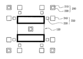
도 6은 본 발명에 따른 오버레이 마크를 나타내는 평면도.6 is a plan view showing an overlay mark according to the present invention;
* 도면의 주요부분에 대한 부호의 설명 *Explanation of symbols on the main parts of the drawings
110 : 코팅 처리부 120 : 얼라인 및 노광 처리부110: coating treatment unit 120: alignment and exposure treatment unit
130 : 현상 처리부 140 : 오버레이 측정장치130: development processing unit 140: overlay measuring device
150 : 칩 영역 160 : 중심선150: chip area 160: centerline
200 : 제 2 오버레이 마크 210 : 제 2 이너 마크200: second overlay mark 210: second inner mark
220 : 제 2 아우터 마크 230 : 제 1 이너 마크220: second outer mark 230: first inner mark
240 : 제 1 아우터 마크 250 : 제 1 오버레이 마크240: first outer mark 250: first overlay mark
본 발명은 오버레이 측정 방법 및 그에 사용되는 오버레이 마크에 관한 것으로, 보다 상세하게는 웨이퍼 상에 초기의 포토 리소그래피 공정이 수행될 경우 오버레이 측정에 의한 오버레이 데이터 산출이 가능한 오버레이 측정 방법 및 그를 사용되는 오버레이 마크에 관한 것이다.The present invention relates to an overlay measurement method and an overlay mark used therein, and more particularly, an overlay measurement method capable of calculating overlay data by overlay measurement when an initial photolithography process is performed on a wafer, and an overlay mark used therein. It is about.
최근, 컴퓨터와 같은 정보 매체의 급속한 보급에 따라 반도체 장치도 비약적으로 발전하고 있다. 그 기능 면에 있어서, 상기 반도체 장치는 고속으로 동작하는 동시에 대용량의 저장 능력을 가질 것이 요구된다. 이러한 요구에 부응하여, 반도체 장치는 집적도, 신뢰도 및 응답 속도 등을 향상시키는 방향으로 제조 기술이 발전되고 있다. In recent years, with the rapid spread of information media such as computers, semiconductor devices are also rapidly developing. In terms of its function, the semiconductor device is required to operate at a high speed and to have a large storage capacity. In response to these demands, manufacturing techniques are being developed for semiconductor devices to improve the degree of integration, reliability, response speed and the like.
이에 따라, 반도체 산업에서 경쟁력 강화를 위한 일환으로 높은 생산 수율을 보장할 수 있는 각각의 단위 공정이 개발되고 있으며, 동시에 각 단위 공정에서의 공정 에러를 측정하는 방법 및 장치도 활발하게 연구되고 있다. 특히 핵심 반도체 제조 공정들 중의 하나인 사진 공정(Photo-lithographic Process)의 경우에도 공정 조건의 변화가 빈번하여 이에 대처할 수 있는 공정 개발 및 이를 수행하기 위한 장치가 필요한 실정이다.Accordingly, each unit process that can guarantee a high production yield is being developed as part of strengthening the competitiveness in the semiconductor industry, and at the same time, methods and apparatuses for measuring process errors in each unit process have been actively studied. In particular, in the case of the photo-lithographic process, which is one of the core semiconductor manufacturing processes, there is a need for a process development and an apparatus for performing the process that can cope with the change in the process conditions frequently.
사진 공정 시에 고려되어야 하는 문제점 중의 하나는 노광 및 현상에 의해 형성되는 포토레지스트 패턴의 미스얼라인(misalign)이다. 상기 미스얼라인은 반도체 장치의 고집적화에 따른 얼라인 마진(align margin)의 축소, 웨이퍼의 대구경화 및 포토 리소그래피 공정의 증가 등에 따라 정확한 얼라인이 점점 어려워지면서, 더욱 심각한 문제점으로 대두되고 있다. 상기 미스얼라인 불량을 방지하기 위해, 웨이퍼에 형성되어 있는 포토레지스트 패턴의 정렬도를 확인하는 작업인 오버레이 측정의 최적화가 필수적으로 요구된다.One of the problems to be considered in the photolithography process is misalignment of the photoresist pattern formed by exposure and development. The misalignment has become a more serious problem as accurate alignment becomes increasingly difficult due to the reduction of the alignment margin due to the high integration of semiconductor devices, the large diameter of the wafer, and the increase of the photolithography process. In order to prevent the misalignment, optimization of overlay measurement, which is an operation of checking the degree of alignment of the photoresist pattern formed on the wafer, is essential.
이와 같은 오버레이 측정을 최적화하기 위한 방법은 미합중국 특허 제5,696,835호 및 제 6,357,131호에 개시되어 있다.Methods for optimizing such overlay measurements are disclosed in US Pat. Nos. 5,696,835 and 6,357,131.
종래의 오버레이 측정방법을 설명하면, 우선, 웨이퍼 상에 포토레지스트 패턴(예를 들어 정렬측정 패턴(alignment measurement pattern))을 형성시키고 하부 패턴층(예를 들어 기준 패턴(reference pattern)과의 중첩된 위치를 측정한다. 이때, 상기 웨이퍼의 각 셀들에 형성된 패턴층들은 너무 복잡하여 오버레이 측정이 이루어질 수 없기 때문에 웨이퍼 칩 영역 외곽의 스크라이브 라인 상에 형성된 오버레이 마크를 이용하여 오버레이 측정이 수행될 수 있다.Referring to the conventional overlay measurement method, first, a photoresist pattern (e.g., an alignment measurement pattern) is formed on a wafer and overlapped with a lower pattern layer (e.g., a reference pattern). In this case, since the pattern layers formed in the cells of the wafer are so complex that overlay measurement cannot be performed, overlay measurement may be performed using overlay marks formed on the scribe line outside the wafer chip area.
상기 오버레이 측정은 일반적으로 하나의 웨이퍼에 구비되는 샷(shot)의 개수에 따른 소정의 비율 또는 웨이퍼의 크기에 따라 수행한다. 또한 상기 웨이퍼의 국부적인 영역이 아니라, 상기 웨이퍼의 전 영역이 포함되도록 측정되는 얼라인 마크들을 지정한다.The overlay measurement is generally performed according to a predetermined ratio or wafer size depending on the number of shots included in one wafer. It also specifies alignment marks that are measured to include the entire area of the wafer, rather than the local area of the wafer.
상기 웨이퍼 상에 형성되어 있는 얼라인 마크에서 측정된 각각의 오버레이 측정 데이터를 회귀분석하여 오버레이 데이터를 산출한다. 상기 오버레이 데이터는 웨이퍼 및 레티클에서 X,Y 방향으로의 틀어진 정도 및 회전 정도를 나타내는 데이터이다. 예컨대, 상기 오버레이 데이터는 웨이퍼 관련 파라미터와, 레티클 관련 파라미터로 나누어진다. 상기 웨이퍼 관련 파라미터는 웨이퍼의 중심을 기준으로 스텝핑 정도가 떨어지는 것으로, 매 샷 이동 시 일정량 씩 점차 변화되면서 밀려 찍히는 것을 의미하며, 레티클 관련 파라미터는 노광장치의 스테이지 성분을 배제했을 때 상기 노광장치의 레티클(reticle) 상의 배율이 노광 시 배율과 달라지는 것을 의미한다.Overlay data is calculated by regression analysis of the respective overlay measurement data measured at the alignment mark formed on the wafer. The overlay data is data indicating the degree of twist and the degree of rotation in the X and Y directions in the wafer and the reticle. For example, the overlay data is divided into wafer related parameters and reticle related parameters. The wafer-related parameter is a stepping degree that is lowered with respect to the center of the wafer, and means that the shot is pushed while being gradually changed by a certain amount during each shot movement. The parameter related to the reticle is the reticle of the exposure apparatus when the stage component of the exposure apparatus is excluded. It means that the magnification on the (reticle) is different from the magnification on exposure.
다음, 오버레이 측정장치는 이와 같이 검출된 오버레이 데이터를 사용하여 보정값을 산출하고, 노광 장치에 피드백하여 이 후에 진행되는 웨이퍼에서 미스 얼라인 불량이 발생되지 않도록 한다.Next, the overlay measuring apparatus calculates a correction value using the detected overlay data, and feeds back to the exposure apparatus so that a misalignment defect does not occur in a subsequent wafer.
하지만, 종래 기술에 따른 오버레이 측정방법은 다음과 같은 문제점이 있었다.However, the overlay measurement method according to the prior art had the following problems.
종래의 오버레이 측정방법은, 웨이퍼 상에 형성되어 있는 얼라인 마크에서 측정된 각각의 오버레이 측정 데이터를 회귀분석하여 오버레이 데이터를 검출한 것이지만, 하부 패턴층이 존재하지 않는 초기 상태의 웨이퍼 상에 형성된 포토레지스트 패턴(액티브 층(Active layer) 또는 첫 번째 층(first layer))의 오버레이 측정 시 오버레이 데이터가 산출되지 않을 수 있기 때문에 생산 수율이 떨어지는 단점이 있었다.Conventional overlay measurement method is a regression analysis of each overlay measurement data measured in the alignment mark formed on the wafer to detect the overlay data, but the photo formed on the wafer in the initial state where the lower pattern layer does not exist The overlay yield of the resist pattern (active layer or first layer) may not be calculated when overlay measurement is performed.
상기와 같은 문제점을 해결하기 위한 본 발명의 목적은, 하부 패턴층이 존재하지 않는 초기 상태의 웨이퍼 상에 형성된 포토레지스트 패턴의 오버레이 측정 시 오버레이 데이터를 산출하여 생산 수율을 증대 또는 극대화할 수 있는 오버레이 측정방법 및 그를 사용한 오버레이 마크를 제공하는 데 있다.An object of the present invention for solving the above problems, an overlay that can increase or maximize the production yield by calculating the overlay data in the overlay measurement of the photoresist pattern formed on the wafer in the initial state where the lower pattern layer does not exist The measurement method and the overlay mark using the same are provided.
상기 목적을 달성하기 위한 본 발명의 양태에 따라, 오버레이 측정방법은, 소정의 단위 공정이 완료된 웨이퍼를 정렬하는 단계; 상기 웨이퍼 상에 형성된 오버레이 마크를 측정하는 단계; 상기 웨이퍼의 오버레이 측정이 처음으로 수행되었는지를 확인하는 단계; 및 상기 오버레이 측정이 처음으로 수행되었을 경우, 상기 웨이퍼의 중심과 상기 오버레이 마크의 중심간의 거리를 이용하여 오버레이 데이터를 검출하는 단계를 포함함을 특징으로 한다.According to an aspect of the present invention for achieving the above object, the overlay measuring method comprises the steps of: aligning a wafer having a predetermined unit process; Measuring an overlay mark formed on the wafer; Confirming whether an overlay measurement of the wafer was performed for the first time; And detecting overlay data using a distance between the center of the wafer and the center of the overlay mark when the overlay measurement is performed for the first time.
또한, 본 발명의 다른 양태는, 소정의 단위 공정이 완료된 웨이퍼를 정렬하는 단계; 상기 웨이퍼 상에 형성된 오버레이 마크를 측정하는 단계; 상기 웨이퍼의 오버레이 측정이 처음으로 수행되었는지를 확인하는 단계; 상기 오버레이 측정이 처음으로 수행되었을 경우, 상기 웨이퍼의 중심과 상기 오버레이 마크의 중심간의 거리를 이용하여 오버레이 데이터를 검출하는 단계; 및 상기 오버레이 데이터가 소정의 오차 범위 내에 존재할 경우, 상기 오버레이 데이터를 이용하여 보상값을 계산하여 후속의 리소그래피 공정에 피드백하여 보정하는 단계를 포함하는 오버레이 측정방법이다.In addition, another aspect of the present invention, the method comprising the steps of aligning the wafer having a predetermined unit process; Measuring an overlay mark formed on the wafer; Confirming whether an overlay measurement of the wafer was performed for the first time; When the overlay measurement is performed for the first time, detecting overlay data using a distance between the center of the wafer and the center of the overlay mark; And if the overlay data is within a predetermined error range, calculating a compensation value using the overlay data and feeding back a correction to a subsequent lithography process.
그리고, 본 발명의 또 다른 양태는, 소정의 단위 공정이 완료된 웨이퍼를 정렬하는 단계; 상기 웨이퍼 상에 형성된 오버레이 마크를 측정하는 단계; 상기 웨이퍼의 오버레이 측정이 처음으로 수행되었는지를 확인하는 단계; 및 상기 오버레이 측정이 처음으로 수행되었을 경우, 상기 웨이퍼의 중심과 상기 오버레이 마크의 중 심간의 거리를 이용하여 오버레이 데이터를 검출하고, 상기 웨이퍼의 오버레이 측정이 복수 번째일 경우, 소정의 오차를 갖는 복수개의 오버레이 마크의 중심간의 거리를 이용하여 오버레이 데이터를 산출하는 단계를 포함하는 오버레이 측정방법이다.In addition, another aspect of the present invention includes the steps of aligning the wafer in which the predetermined unit process is completed; Measuring an overlay mark formed on the wafer; Confirming whether an overlay measurement of the wafer was performed for the first time; And when overlay measurement is performed for the first time, overlay data is detected by using a distance between the center of the wafer and the center of the overlay mark, and when the overlay measurement of the wafer is plural, Calculating overlay data using a distance between centers of two overlay marks.
마지막으로, 본 발명의 또 다른 양태는, 소자가 형성될 웨이퍼 칩 영역의 외곽에 제 1 이너 마크 또는 제 1 아우터 마크가 각각 별도로 형성된 제 1 오버레이 마크; 및 초기의 웨이퍼 리소그래피 공정에 의해 상기 칩 영역 외곽의 모서리에서 그 중심이 일치되는 제 2 이너 마크 및 제 2 아우터 마크가 형성된 적어도 하나이상의 제 2 오버레이 마크를 포함하는 오버레이 측정에 사용되는 오버레이 마크이다.
Lastly, another aspect of the present invention provides a display device comprising: a first overlay mark each having a first inner mark or a first outer mark separately formed on an outer side of a wafer chip region where an element is to be formed; And at least one second overlay mark having a second inner mark and a second outer mark whose centers coincide with each other at an edge outside the chip region by an initial wafer lithography process.
이하, 첨부 도면을 참조하여 본 발명의 실시예를 상세히 설명한다. 그러나, 본 발명의 실시예들은 여러 가지 다른 형태로 변형될 수 있으며, 본 발명의 범위가 아래에서 상술하는 실시예들로 인해 한정되어지는 것으로 해석되어져서는 안 된다. 본 발명의 실시예들은 당업계에서 평균적인 지식을 가진 자에게 본 발명을 보다 완전하게 설명하기 위해서 제공되어지는 것이다. 따라서, 도면에서의 요소의 형상 등은 보다 명확한 설명을 강조하기 위해서 과장되어진 것이며, 도면상에서 동일한 부호로 표시된 요소는 동일한 요소를 의미한다. 그리고 본 발명을 설명함에 있어서, 관련된 공지 기능 혹은 구성에 대한 구체적인 설명이 본 발명의 요지를 불필요하게 흐릴 수 있다고 판단되는 경우 그 상세한 설명을 생략한다.Hereinafter, embodiments of the present invention will be described in detail with reference to the accompanying drawings. However, embodiments of the present invention may be modified in many different forms, and the scope of the present invention should not be construed as being limited by the embodiments described below. Embodiments of the present invention are provided to more completely explain the present invention to those skilled in the art. Accordingly, the shape and the like of the elements in the drawings are exaggerated to emphasize a more clear description, and the elements denoted by the same reference numerals in the drawings means the same elements. In the following description of the present invention, if it is determined that a detailed description of a related known function or configuration may unnecessarily obscure the subject matter of the present invention, the detailed description thereof will be omitted.
도 1은 본 발명의 실시예에 따른 오버레이 측정방법을 설명하기 위한 흐름도이다. 1 is a flowchart illustrating an overlay measurement method according to an embodiment of the present invention.
도 1에 도시된 바와 같이, 본 발명에 따른 오버레이 측정방법은, 먼저, 소정의 포토 리소그래피 공정이 완료된 웨이퍼(W)를 정렬한다. 상기 웨이퍼(W)는 상기 웨이퍼(W)에 형성된 플랫존 또는 노치를 기준으로 일방향으로 정렬된다. 이때, 상기 웨이퍼(W)의 중심 위치가 결정되어진다.As shown in FIG. 1, in the overlay measuring method according to the present invention, first, a wafer W on which a predetermined photolithography process is completed is aligned. The wafer W is aligned in one direction based on the flat zone or notch formed in the wafer W. At this time, the center position of the wafer W is determined.
다음, 상기 웨이퍼(W) 상에서 오버레이 측정이 수행되어야할 다수의 부위를 샘플링하고, 상기 샘플링된 부위들에서 각 오버레이 마크를 측정한다. 상기 웨이퍼(W)에는 다수개의 칩영역 및 오버레이 마크가 형성되어 있지만, 이들을 모두 측정하기 위한 시간과 생산성이 떨어지기 때문에 상기 웨이퍼(W)의 전면에서 무작위로 고르게 샘플링하여 오버레이 측정이 수행된다. 예컨대, 30센치(12인치) 지름을 갖는 웨이퍼(W)의 경우, 약 20에서 40회정도의 오버레이 측정이 수행되는 데, 바람직하게는 약 29번 정도로 수행된다. Next, a plurality of areas are to be sampled on which the overlay measurement is to be performed on the wafer W, and each overlay mark is measured at the sampled areas. Although a plurality of chip areas and overlay marks are formed on the wafer W, since time and productivity for measuring them are all reduced, overlay measurement is performed by randomly and evenly sampling the front surface of the wafer W. For example, in the case of a wafer W having a diameter of 30 centimeters (12 inches), overlay measurements of about 20 to 40 times are performed, preferably about 29 times.
그 다음, 이전의 단위 공정 수행 시의 히스토리 데이터로부터 해당 웨이퍼(W)의 오버레이 측정이 처음 수행되는지를 확인한다. 상기 웨이퍼(W)가 포토 리소그래피 공정을 처음 수행할 경우, 상기 히스토리 데이터에는 상기 웨이퍼(W)가 오버레이 측정을 한 결과가 없지만, 상기 웨이퍼(W)가 이전에 적어도 한번 이상의 포토 리소그래피 공정을 수행하였을 경우, 상기 히스토리 데이터는 상기 웨이퍼(W)가 오버레이 측정한 결과를 가지고 있다.Then, it is checked whether the overlay measurement of the wafer W is performed for the first time from the historical data of the previous unit process. When the wafer W first performs a photolithography process, the history data does not have an overlay measurement result of the wafer W. However, the wafer W may have previously performed at least one photolithography process. In this case, the history data has a result of overlay measurement of the wafer (W).
그후, 상기 웨이퍼(W)가 포토 리소그래피 공정을 처음으로 수행했을 경우, 상기 웨이퍼(W)의 중심과 오버레이 마크의 중심간의 거리를 이용하여 오버레이 데이터를 계산한다. 예컨대, 상기 오버레이 데이터는 웨이퍼 관련 파라미터 및 레티클 관련 데이터로 나누어진다. 반면, 상기 웨이퍼(W)가 이전에 포토 리소그래피 공정을 적어도 한번이상 수행했을 경우, 현 포토 리소그래피 공정에서의 포토레지스트 패턴(예를 들어 정렬측정 패턴(alignment measurement pattern)) 오버레이 마크의 중심과, 하부 패턴층(예를 들어 기준 패턴(reference pattern) 오버레이 마크의 중심간의 거리를 이용하여 오버레이 데이터를 산출한다.Then, when the wafer W first performs a photolithography process, overlay data is calculated using the distance between the center of the wafer W and the center of the overlay mark. For example, the overlay data is divided into wafer related parameters and reticle related data. On the other hand, when the wafer W has previously performed the photolithography process at least once, the center of the photoresist pattern (for example, alignment measurement pattern) overlay mark and the bottom of the current photolithography process, The overlay data is calculated using the distance between the centers of the pattern layers (eg, reference pattern overlay marks).
그리고, 상기 오버레이 데이터가 일정한 오차 범위 내에 존재할 경우, 상기 오버레이 데이터를 이용하여 보상값을 계산하여 후속의 포토 리소그래피 공정에서 노광설비에 적용토록 할 수 있다.When the overlay data exists within a certain error range, a compensation value may be calculated using the overlay data to be applied to an exposure apparatus in a subsequent photolithography process.
마지막으로 상기 오버레이 데이터가 상기 오차 범위밖에 있을 경우, 상기 웨이퍼(W)의 포토 리소그래피 공정을 재작업시켜야 한다.Finally, if the overlay data is outside the error range, the photolithography process of the wafer W must be reworked.
따라서, 본 발명에 따른 오버레이 측정방법은, 하부 패턴층이 존재하지 않는 초기 상태의 웨이퍼(W) 상에 형성된 포토레지스트 패턴(액티브 층(Active layer) 또는 첫 번째 층(first layer))의 오버레이 측정 시 웨이퍼(W)의 중심과 오버레이 마크의 중심간의 거리를 이용하여 오버레이 데이터를 산출하고 후속의 포토 리소그래피 공정을 수행토록 할 수 있기 때문에 생산 수율을 증대 또는 극대화할 수 있다.Therefore, in the overlay measurement method according to the present invention, the overlay measurement of the photoresist pattern (active layer or first layer) formed on the wafer W in the initial state in which the lower pattern layer does not exist. By using the distance between the center of the test wafer W and the center of the overlay mark, the overlay data can be calculated and a subsequent photolithography process can be performed to increase or maximize production yield.
한편, 포토 리소그래피 공정은 크게 코팅 공정, 얼라인 및 노광 공정, 현상 공 정, 오버레이 검사로 구분될 수 있다. 이때, 이들 공정은 스피너 설비, 스텝퍼, 스케너 또는 전자 현미경(Scanning Electron Spectroscopy)과 같은 장비를 통하여 수행된다.On the other hand, the photolithography process can be largely divided into coating process, alignment and exposure process, development process, overlay inspection. At this time, these processes are performed through equipment such as spinner equipment, steppers, scanners or scanning electron spectroscopy.
도 2는 포토 리소그래피 공정을 수행하기 위한 장비에서의 공정 순서를 개략적으로 나타낸 블록도로서, 먼저, 스피너 설비의 코팅 처리부(110)에서는 웨이퍼(W) 표면의 습기를 제거하고, 도포될 포토레지스트와 웨이퍼(W) 표면과의 밀착성을 증가시키기 위하여 프리 베이크 공정과 고압 순수와 브러쉬를 이용하여 웨이퍼(W) 표면의 불순물을 제거하는 스크러빙공정, 균일한 코팅을 위한 스핀공정, 솔벤트를 휘발시키고 포토레지스트를 경화시키는 소프트 베이크 공정 등을 수행한다.FIG. 2 is a block diagram schematically illustrating a process sequence in an apparatus for performing a photolithography process. First, in the
이후, 얼라인 및 노광 처리부(120)는 스텝퍼의 기준마크에 의해 레티클을 정렬시키고, 웨이퍼(W)와 레티클을 정렬시키는 프리 얼라인공정, 웨이퍼(W)의 플랫존을 고정시키는 얼라인 공정, 노출량을 결정하여 포토레지스트를 노광시키는 노광공정등을 포함하여 이루어진다.Subsequently, the alignment and
그리고, 현상 처리부(130)에서는 정재파 효과를 제거하는 포스트 노광공정, UV광과 반응한 부분을 선택적으로 제거하는 현상공정, 웨이퍼(W)에 남겨진 포토레지스트 패턴이 충분히 열적 환경에 견딜 수 있도록 경화시키는 하드 베이크 공정 등을 수행한다.In addition, the developing
다음, 상기 오버레이 측정장치(140)는 상기 노광설비를 통하여 웨이퍼(W)상에 포토레지스트 패턴를 형성시킨 다음에 하부 패턴층과의 오버레이를 측정하여 오버레이 측정 데이터를 검출하고, 상기 오버레이 측정 데이터를 이용하여 오버레이 데 이터를 산출하고, 보정값을 계산하여 후속의 상기 얼라인 및 노광 처리부(120)로 피드백 한다. 상기 오버레이 측정은 상기 포토레지스트 패턴이 정확한 위치에 형성되었는지를 확인하는 작업으로서, 포토 미스얼라인 불량 방지를 위해 반드시 필요한 작업이다. 상기 오버레이 측정장치(140)에서 오버레이 측정이 처음으로 진행되는 해당 웨이퍼(W)에 대해서는 상기 하부 패턴층이 형성되어 있지 않아 오버레이 측정이 불가능하여 기존에는 오버레이 데이터를 산출하는 것이 불가능했다. 그러나, 본 발명의 오버레이 측정방법은 먼저, 오버레이 측정이 처음으로 진행되는 해당 웨이퍼(W)의 오버레이 마크의 위치를 검출하고, 그후, 검출된 오버레이 마크의 중심과 웨이퍼(W)의 중심간의 거리를 이용하여 오버레이 데이터를 산출하여 후속의 얼라인 및 노광처리부(120)에 피드백할 수 있다.Next, the
오버레이 측정 이후, 전자 현미경을 이용하여 포토레지스터 패턴의 현상후 정밀 검사(After Develop Inspection : ADI)를 수행하고, 후속의 열처리를 통한 상기 포토레지스터 패턴의 재유동(reflow) 공정이 수행될 경우 유동후 정밀검사(After Flow Inspection : AFI)를 수행할 수도 있다.After overlay measurement, after developing inspection (ADI) of the photoresist pattern is performed by using an electron microscope, and after the flow if the reflow process of the photoresist pattern through a subsequent heat treatment is performed After flow inspection (AFI) may be performed.
일반적으로, 상기 오버레이 데이터는 상기 웨이퍼(W)의 지정된 위치(예컨대 중심)로부터 각 마크의 중심부까지의 거리인 x,y 와, 웨이퍼(W)(W) 상에 형성된 얼라인먼트 마크들에서 하부 패턴층에 형성된 외측 마크(outer mark)와 상부 패턴층에 형성된 내측 마크(inner mark) 사이의 dx/dy를 측정한 다음, 이하에서의 회귀분석 수식들을 통해 추출할 수 있다.In general, the overlay data is the bottom pattern layer in x, y, which is the distance from the designated position (eg, the center) of the wafer W to the center of each mark, and the alignment marks formed on the wafer W (W). The dx / dy between the outer mark formed on the inner mark and the inner mark formed on the upper pattern layer may be measured, and then extracted through the following regression equations.
도 3 내지 도 5는 오버레이 데이터를 설명하기 위해 나타낸 평면도로서, 상기 오버레이 데이터는 웨이퍼 관련 파라미터와 레티클 관련 파라미터로 구분된다. 상기 웨이퍼 관련 파라미터는 웨이퍼(W)의 중심을 기준으로 스템핑 정도가 떨어져 매 샷의 이동 시 일정량씩 점차 증가 또는 감소되면서 밀려서 찍히는 것을 의미하며, 도 3의 화살표 방향으로 상기 웨이퍼(W)의 팽창 또는 수축에 의해서 나타날 때가 있다. 여기서, 웨이퍼(W)의 중심을 지나는 중심선(160)을 기준으로 상기 화살표의 방향을 따라 칩 영역(150)이 팽창하여 나타남을 알 수 있다. 이때, 상기 웨이퍼 관련 파라미터의 발생원인으로는 스텝퍼 설비에서의 입력값 에러, 스피너 설비에서의 베이크에 의한 수축 팽창, 노광설비에서의 정렬 마크의 상태 및 신호 검출 불량 또는 웨이퍼(W) 상에 형성된 막질의 변화량이 주요한 요인이 된다. 또한, 웨이퍼 관련 파라미터를 자세하게 살펴보면, 오버레이 마크가 좌우, 상하로 어긋난 정도를 보는 오프셋(offset)성분과, 렌즈에 의해 웨이퍼(W) 상의 형성된 패턴이 좌우, 상하로 확대된 정도를 보는 스케일링(scaling)성분과, 오버레이 마크의 중심축이 웨이퍼(W) 중심축에 대해 회전되어 틀어진 정도를 보는 회전(rotation)성분과, 오버레이 마크의 중심축간에 서로 틀어진 정도를 보는 직교(orthogonal)성분들로 구분될 수 있다. 3 to 5 are plan views illustrating overlay data, wherein the overlay data is divided into wafer related parameters and reticle related parameters. The wafer-related parameter means that the stamping degree is lowered with respect to the center of the wafer W, and is pushed and taken while being gradually increased or decreased by a certain amount during each movement of the shot, and the wafer W is expanded in the direction of the arrow of FIG. 3. Or by contraction. Here, it can be seen that the
따라서, 웨이퍼 관련 파라미터는 두 개의 x, y성분을 갖는 평면 직교 좌표계를 이용하여 회귀분석 수식1로 나타낼 수 있다.Therefore, the wafer-related parameters can be represented by regression equation 1 using a planar Cartesian coordinate system having two x and y components.
(수식1)(Formula 1)
dx= Xoff + Xsca * x - Xrot * ydx = Xoff + Xsca * x-Xrot * y
dy= Yoff + Ysca * y - Xrot * xdy = Yoff + Ysca * y-Xrot * x
이때, x방향에서 Xoff는 웨이퍼 오프셋, Xsca는 웨이퍼 스켈링, Xrot는 웨이퍼 회전이고, y방향에서 Yoff는 웨이퍼 오프셋, Ysca는 웨이퍼 스켈링, Yrot는 웨이퍼 회전을 나타내는 상수이다. 또한, 복수개의 오버레이 마크 측정에 따른 누적수식은 각 변수(x,y,dx,dy)에 대한 수열로서 변환될 수 있다.In this case, Xoff is a wafer offset, Xsca is a wafer scaling, Xrot is a wafer rotation, Yoff is a wafer offset, Ysca is a wafer scaling, and Yrot is a constant representing wafer rotation. In addition, the cumulative equation according to the plurality of overlay mark measurements may be converted as a sequence for each variable (x, y, dx, dy).
반면, 레티클 관련 파라미터는 노광설비의 스테이지 성분을 배제하였을 때 레티클 상의 배율이 노광 설비에서의 노광 시점에 비해 배율이 커진 상태 또는 적어진 상태를 의미하며, 도 4 내지 도 5에서 웨이퍼(W)에 형성된 각 셀에서 화살표 방향으로 팽창 또는 수축에 의해 나타날 수 있다. 여기서, 웨이퍼(W)의 중심에 위치한 칩 영역(150)이 중심선(160)을 기준으로 사방으로 팽창하여 나타남을 알 수 있다. 물론, 상기 중심선(160)이 지나지 않는 각 칩 영역(150)에서의 팽창 또는 수축을 나타낼 수도 있다. 이때, 상기 레티클 관련 파라미터의 발생원인은 해당 웨이퍼(W)의 오버레이 측정이 처음으로 진행될 경우 노광 설비 광학계의 정밀도, 해당 웨이퍼(W) 오버레이 측정이 적어도 두 번째 이상 진행될 경우 노광 설비 광학계의 미스얼라인 또는 레티클의 오버레이 마크 불량이 될 수 있다. 또한, 레티클 관련 파라미터를 자세하게 살펴보면, 노광 설비에서의 레티클의 배율이 노광 시 증감됨에 의해 상하로 확대된 정도를 보는 레티클 축소(reduction)성분과, 상기 레티클이 부정확하게 세팅되어 얼라인먼트 패턴의 축이 얼라인먼트 기준축에 대해 틀어진 정도를 보는 레티클 회전(rotation)성분으로 구분될 수 있다. 마찬가지로, 레티클 관련 파라미터는 두 개의 x, y성분을 갖는 평면 직교 좌표계를 이용하여 회귀분석 수식2로 나타낼 수 있다.On the other hand, the parameter related to the reticle refers to a state in which the magnification on the reticle is larger or smaller than the exposure time of the exposure apparatus when the stage component of the exposure apparatus is excluded, and the wafer W is illustrated in FIGS. 4 to 5. Each cell formed can be manifested by expansion or contraction in the direction of the arrow. Here, it can be seen that the
(수식2)(Formula 2)
dx= Xred * x - Xrot * ydx = Xred * x-Xrot * y
dy= Yred * y - Xrot * xdy = Yred * y-Xrot * x
이때, x방향에서 Xred는 레티클 축소(reduction), Xrot는 레티클 회전이고, y방향에서 Yred는 레티클 축소, Yrot는 레티클 회전을 나타내는 상수이다. 마찬가지로, 복수개의 오버레이 마크 측정에 따른 누적수식은 각 변수(x,y,dx,dy)에 대한 수열로서 변환될 수 있다.In this case, Xred is a reticle reduction in the x direction, Xrot is a reticle rotation, Yred is a reticle reduction in the y direction, and Yrot is a constant indicating a reticle rotation. Similarly, the cumulative equation according to the plurality of overlay mark measurements can be converted as a sequence for each variable (x, y, dx, dy).
한편, 상기 웨이퍼(W)의 오버레이 측정이 이와 같은 오버레이 데이터를 이용하여 웨이퍼(W) 초기 이너 마크와 아우터 마크가 필수적으로 요구된다. On the other hand, the overlay measurement of the wafer (W) using the overlay data, such as the initial inner mark and the outer mark of the wafer (W) is essentially required.
도 6은 본 발명에 따른 오버레이 마크를 나타내는 평면도로서, 본 발명의 오버레이 마크는 소자가 형성될 웨이퍼(W) 칩 영역(150)의 외곽에 제 1 이너 마크(230) 또는 제 1 아우터 마크(240)가 각각 별도로 형성된 제 1 오버레이 마크(250)와, 초기의 웨이퍼(W) 포토 리소그래피 공정에 의해 상기 칩 영역(150)외곽의 모서리에서 그 중심이 일치되는 제 2 이너 마크(210) 및 제 2 아우터 마크(220)가 형성된 제 2 오버레이 마크(200)를 포함하여 구성된다.FIG. 6 is a plan view illustrating an overlay mark according to the present invention, wherein the overlay mark of the present invention may include a first
여기서, 제 1 오버레이 마크(250)는 기존의 하부 패턴층 및 상기 하부 패턴층 상부에 형성되는 포토레지스트 패턴을 이용하여 오버레이 마크들간의 거리를 이용하여 오버레이 데이터를 산출하기 위한 것이다.Here, the
반면, 제 2 오버레이 마크(200)는 하부 패턴층이 존재하지 않는 초기(bare) 웨이퍼(W) 상에 형성된 포토레지스트 패턴의 오버레이 측정 시 오버레이 측정 장치에 서 오버레이 마크의 중심을 인식토록 할 수 있다. On the other hand, the
즉, 오버레이 측정장치(140)는 제 1 이너 마크(230) 및 제 1 아우터 마크(240)가 형성된 하부 패턴층과, 상기 하부 패턴층에 배타적으로 제 1 아우터 마크(240) 및 제 1 이너 마크(230)가 형성된 현 포토레지스트 패턴의 오버레이를 측정하여 각각의 상기 제 1 이너 마크(230)의 중심과 제 1 아우터 마크(240)의 중심간의 거리를 이용하여 오버레이 데이터를 산출할 수 있다. 또한, 초기의(bare) 웨이퍼(W) 상에 형성된 제 2 오버레이 마크(200)를 갖는 포토레지스트 패턴의 경우, 상기 오버레이 측정장치(140)에서 중심이 일치된 제 2 이너 마크(210)와 제 2 아우터 마크(220)를 인식하여 오버레이 측정 데이터를 검출하고, 상기 제 2 오버레이 마크(200)의 중심과 웨이퍼(W) 중심간의 거리를 이용하여 오버레이 데이터를 산출할 수 있다.That is, the
이때, 상기 제 2 오버레이 마크(200)는 상기 칩 영역(150)의 중심(예컨대, 4뱅크로 이루어진 셀 영역간의 코어 페리영역)에 형성되어 상기 제 2 오버레이 마크(200)의 중심과 웨이퍼(W) 중심간의 거리를 이용한 오버레이 데이터 산출 시 용이하게 사용될 수 있다.In this case, the
따라서, 본 발명에 따른 오버레이 마크는 기존의 중심이 다른 이너 마크 또는 아우터 마크로 이루어진 제 1 오버레이 마크(250)와, 초기 웨이퍼(W)의 포토 리소그래피 공정 시 하나의 중심을 갖는 이너 마크와 아우터 마크로 이루어진 제 2 오버레이 마크(200)를 이용하여 오버레이 측정장치(140)로 하여금 오버레이 데이터를 산출토록 할 수 있기 때문에 생산 수율을 증대 또는 극대화할 수 있다.Accordingly, the overlay mark according to the present invention includes a
또한, 상기한 실시예의 설명은 본 발명의 더욱 철저한 이해를 제공하기 위하여 도면을 참조로 예를 든 것에 불과하므로, 본 발명을 한정하는 의미로 해석되어서는 안될 것이다. 그리고, 본 발명의 기술분야에서 통상의 지식을 가진 자에게 있어 본 발명의 기본적 원리를 벗어나지 않는 범위 내에서 다양한 변화와 변경이 가능하다. 예컨대, 제 2 오버레이 마크(200)는 칩 영역(150)의 외곽에 어디에 설계되어도 무방함은 물론이다.In addition, the description of the above embodiment is merely given by way of example with reference to the drawings in order to provide a more thorough understanding of the present invention, it should not be construed as limiting the present invention. In addition, various changes and modifications can be made by those skilled in the art without departing from the basic principles of the present invention. For example, the
상술한 바와 같이 본 발명에 의하면, 하부 패턴층이 존재하지 않는 초기 상태의 웨이퍼 상에 형성된 포토레지스트 패턴의 오버레이 측정 시 웨이퍼의 중심과 오버레이 마크의 중심간의 거리를 이용하여 오버레이 데이터를 산출하고 후속의 포토 리소그래피 공정을 수행토록 할 수 있기 때문에 생산 수율을 증대 또는 극대화할 수 있는 효과가 있다.As described above, according to the present invention, the overlay data is calculated by using the distance between the center of the wafer and the center of the overlay mark when measuring the overlay of the photoresist pattern formed on the wafer in the initial state in which the lower pattern layer does not exist. Since the photolithography process can be performed, the production yield can be increased or maximized.
Claims (19)
Priority Applications (2)
| Application Number | Priority Date | Filing Date | Title |
|---|---|---|---|
| KR1020040079766A KR100577568B1 (en) | 2004-10-07 | 2004-10-07 | Overlay measurement method and overlay mark used |
| US11/235,173 US7483156B2 (en) | 2004-10-07 | 2005-09-27 | Method for measuring overlay and overlay mark used therefor |
Applications Claiming Priority (1)
| Application Number | Priority Date | Filing Date | Title |
|---|---|---|---|
| KR1020040079766A KR100577568B1 (en) | 2004-10-07 | 2004-10-07 | Overlay measurement method and overlay mark used |
Publications (2)
| Publication Number | Publication Date |
|---|---|
| KR20060030930A KR20060030930A (en) | 2006-04-12 |
| KR100577568B1 true KR100577568B1 (en) | 2006-05-08 |
Family
ID=36145758
Family Applications (1)
| Application Number | Title | Priority Date | Filing Date |
|---|---|---|---|
| KR1020040079766A Expired - Fee Related KR100577568B1 (en) | 2004-10-07 | 2004-10-07 | Overlay measurement method and overlay mark used |
Country Status (2)
| Country | Link |
|---|---|
| US (1) | US7483156B2 (en) |
| KR (1) | KR100577568B1 (en) |
Families Citing this family (9)
| Publication number | Priority date | Publication date | Assignee | Title |
|---|---|---|---|---|
| KR100850145B1 (en) * | 2006-12-27 | 2008-08-04 | 동부일렉트로닉스 주식회사 | Overlay component correction method in semiconductor overlay measurement equipment |
| US7684038B1 (en) * | 2008-04-04 | 2010-03-23 | Kla-Tencor Corporation | Overlay metrology target |
| US8786054B2 (en) * | 2009-11-16 | 2014-07-22 | Taiwan Semiconductor Manufacturing Company, Ltd. | Structure for integrated circuit alignment |
| KR101675380B1 (en) * | 2010-02-19 | 2016-11-14 | 삼성전자주식회사 | method for correcting overlay and manufacturing method of semiconductor device used the same |
| CN103247550B (en) * | 2013-05-07 | 2016-04-13 | 上海华力微电子有限公司 | The test module of monitoring program stability and method |
| US9354527B2 (en) * | 2013-08-01 | 2016-05-31 | Kabushiki Kaisha Toshiba | Overlay displacement amount measuring method, positional displacement amount measuring method and positional displacement amount measuring apparatus |
| US12354971B2 (en) | 2021-09-08 | 2025-07-08 | Changxin Memory Technologies, Inc. | Semiconductor structure, method for manufacturing same and memory |
| CN115775720B (en) * | 2021-09-08 | 2025-06-06 | 长鑫存储技术有限公司 | Semiconductor structure and manufacturing method thereof, and memory |
| KR20250015898A (en) * | 2023-07-24 | 2025-02-03 | 캐논 가부시끼가이샤 | Lithography method, article manufacturing method, information processing method, computer program, and information processing apparatus |
Citations (1)
| Publication number | Priority date | Publication date | Assignee | Title |
|---|---|---|---|---|
| JPH09246157A (en) * | 1996-03-08 | 1997-09-19 | Hitachi Ltd | Photomask alignment method and exposure apparatus |
Family Cites Families (6)
| Publication number | Priority date | Publication date | Assignee | Title |
|---|---|---|---|---|
| KR0170909B1 (en) * | 1995-09-27 | 1999-03-30 | 김주용 | Overlay detecting method of semiconductor device |
| US6266144B1 (en) | 1999-08-26 | 2001-07-24 | Taiwan Semiconductor Manufacturing Company | Stepper and scanner new exposure sequence with intra-field correction |
| US6357131B1 (en) | 1999-12-20 | 2002-03-19 | Taiwan Semiconductor Manufacturing Company | Overlay reliability monitor |
| JP2001189263A (en) | 1999-12-28 | 2001-07-10 | Toshiba Corp | Misalignment inspection method and charged beam exposure method |
| US6218200B1 (en) * | 2000-07-14 | 2001-04-17 | Motorola, Inc. | Multi-layer registration control for photolithography processes |
| DE10224164B4 (en) * | 2002-05-31 | 2007-05-10 | Advanced Micro Devices, Inc., Sunnyvale | A two-dimensional structure for determining a superposition accuracy by means of scattering measurement |
-
2004
- 2004-10-07 KR KR1020040079766A patent/KR100577568B1/en not_active Expired - Fee Related
-
2005
- 2005-09-27 US US11/235,173 patent/US7483156B2/en not_active Expired - Fee Related
Patent Citations (1)
| Publication number | Priority date | Publication date | Assignee | Title |
|---|---|---|---|---|
| JPH09246157A (en) * | 1996-03-08 | 1997-09-19 | Hitachi Ltd | Photomask alignment method and exposure apparatus |
Also Published As
| Publication number | Publication date |
|---|---|
| KR20060030930A (en) | 2006-04-12 |
| US7483156B2 (en) | 2009-01-27 |
| US20060078808A1 (en) | 2006-04-13 |
Similar Documents
| Publication | Publication Date | Title |
|---|---|---|
| US7666559B2 (en) | Structure and method for determining an overlay accuracy | |
| US6975974B2 (en) | Overlay error model, sampling strategy and associated equipment for implementation | |
| US20110051150A1 (en) | Unique mark and method to determine critical dimension uniformity and registration of reticles combined with wafer overlay capability | |
| KR102124896B1 (en) | Indirect determination of processing parameters | |
| US7288848B2 (en) | Overlay mark for measuring and correcting alignment errors | |
| KR100439472B1 (en) | Method and apparatus for measuring of processing error and method and apparatus for measuring of overlay | |
| KR100577568B1 (en) | Overlay measurement method and overlay mark used | |
| US7084962B2 (en) | Method for detecting positioning errors of circuit patterns during the transfer by means of a mask into layers of a substrate of a semiconductor wafer | |
| CN113611650A (en) | Method for aligning wafer pattern | |
| US20150116686A1 (en) | Edge-dominant alignment method in exposure scanner system | |
| US6727989B1 (en) | Enhanced overlay measurement marks for overlay alignment and exposure tool condition control | |
| JP2003017386A (en) | Alignment method, exposure method, exposure apparatus and device manufacturing method | |
| CN100399529C (en) | Detection device and detection method for exposure machine | |
| KR100714266B1 (en) | Image correction method in manufacturing process of semiconductor device | |
| CN105759563B (en) | Photomask and method for detecting photomask or wafer contamination | |
| KR20030016458A (en) | method for inter-locking tool induce shift data in overlay measuring apparatus | |
| JPH07283109A (en) | Exposure method of semiconductor device and aligner | |
| KR960002287B1 (en) | Stepping pitch measuring method of alignment/exposure apparatus | |
| KR100576425B1 (en) | Overlay Measurement Method Using Photosensitive Film Thickness | |
| KR20050069212A (en) | Stepper and method for aligning shot using the same | |
| JP2005310833A (en) | Substrate-testing apparatus and method | |
| US7175951B1 (en) | Two mask in-situ overlay checking method | |
| KR100375290B1 (en) | Method of analyzing factor responsible for errors in wafer pattern, and apparatus for producing photolithographic mask | |
| US20030211411A1 (en) | Method for monitoring focus in lithography | |
| KR20070095034A (en) | Overlay measurement method |
Legal Events
| Date | Code | Title | Description |
|---|---|---|---|
| A201 | Request for examination | ||
| PA0109 | Patent application |
St.27 status event code: A-0-1-A10-A12-nap-PA0109 |
|
| PA0201 | Request for examination |
St.27 status event code: A-1-2-D10-D11-exm-PA0201 |
|
| PN2301 | Change of applicant |
St.27 status event code: A-3-3-R10-R13-asn-PN2301 St.27 status event code: A-3-3-R10-R11-asn-PN2301 |
|
| PN2301 | Change of applicant |
St.27 status event code: A-3-3-R10-R13-asn-PN2301 St.27 status event code: A-3-3-R10-R11-asn-PN2301 |
|
| D13-X000 | Search requested |
St.27 status event code: A-1-2-D10-D13-srh-X000 |
|
| D14-X000 | Search report completed |
St.27 status event code: A-1-2-D10-D14-srh-X000 |
|
| E902 | Notification of reason for refusal | ||
| PE0902 | Notice of grounds for rejection |
St.27 status event code: A-1-2-D10-D21-exm-PE0902 |
|
| PG1501 | Laying open of application |
St.27 status event code: A-1-1-Q10-Q12-nap-PG1501 |
|
| P11-X000 | Amendment of application requested |
St.27 status event code: A-2-2-P10-P11-nap-X000 |
|
| P13-X000 | Application amended |
St.27 status event code: A-2-2-P10-P13-nap-X000 |
|
| E701 | Decision to grant or registration of patent right | ||
| PE0701 | Decision of registration |
St.27 status event code: A-1-2-D10-D22-exm-PE0701 |
|
| GRNT | Written decision to grant | ||
| PR0701 | Registration of establishment |
St.27 status event code: A-2-4-F10-F11-exm-PR0701 |
|
| PR1002 | Payment of registration fee |
St.27 status event code: A-2-2-U10-U11-oth-PR1002 Fee payment year number: 1 |
|
| PG1601 | Publication of registration |
St.27 status event code: A-4-4-Q10-Q13-nap-PG1601 |
|
| PR1001 | Payment of annual fee |
St.27 status event code: A-4-4-U10-U11-oth-PR1001 Fee payment year number: 4 |
|
| PR1001 | Payment of annual fee |
St.27 status event code: A-4-4-U10-U11-oth-PR1001 Fee payment year number: 5 |
|
| PR1001 | Payment of annual fee |
St.27 status event code: A-4-4-U10-U11-oth-PR1001 Fee payment year number: 6 |
|
| PR1001 | Payment of annual fee |
St.27 status event code: A-4-4-U10-U11-oth-PR1001 Fee payment year number: 7 |
|
| R18-X000 | Changes to party contact information recorded |
St.27 status event code: A-5-5-R10-R18-oth-X000 |
|
| FPAY | Annual fee payment |
Payment date: 20130430 Year of fee payment: 8 |
|
| PR1001 | Payment of annual fee |
St.27 status event code: A-4-4-U10-U11-oth-PR1001 Fee payment year number: 8 |
|
| FPAY | Annual fee payment |
Payment date: 20140430 Year of fee payment: 9 |
|
| PR1001 | Payment of annual fee |
St.27 status event code: A-4-4-U10-U11-oth-PR1001 Fee payment year number: 9 |
|
| LAPS | Lapse due to unpaid annual fee | ||
| PC1903 | Unpaid annual fee |
St.27 status event code: A-4-4-U10-U13-oth-PC1903 Not in force date: 20150502 Payment event data comment text: Termination Category : DEFAULT_OF_REGISTRATION_FEE |
|
| PC1903 | Unpaid annual fee |
St.27 status event code: N-4-6-H10-H13-oth-PC1903 Ip right cessation event data comment text: Termination Category : DEFAULT_OF_REGISTRATION_FEE Not in force date: 20150502 |
|
| P22-X000 | Classification modified |
St.27 status event code: A-4-4-P10-P22-nap-X000 |
|
| P22-X000 | Classification modified |
St.27 status event code: A-4-4-P10-P22-nap-X000 |