KR100560773B1 - Semiconductor memory device capable of controlling burst length without resetting the operating mode and memory system comprising the same - Google Patents
Semiconductor memory device capable of controlling burst length without resetting the operating mode and memory system comprising the same Download PDFInfo
- Publication number
- KR100560773B1 KR100560773B1 KR1020030070311A KR20030070311A KR100560773B1 KR 100560773 B1 KR100560773 B1 KR 100560773B1 KR 1020030070311 A KR1020030070311 A KR 1020030070311A KR 20030070311 A KR20030070311 A KR 20030070311A KR 100560773 B1 KR100560773 B1 KR 100560773B1
- Authority
- KR
- South Korea
- Prior art keywords
- burst
- read
- address
- circuit
- burst length
- Prior art date
- Legal status (The legal status is an assumption and is not a legal conclusion. Google has not performed a legal analysis and makes no representation as to the accuracy of the status listed.)
- Expired - Fee Related
Links
Images


Classifications
-
- G—PHYSICS
- G11—INFORMATION STORAGE
- G11C—STATIC STORES
- G11C11/00—Digital stores characterised by the use of particular electric or magnetic storage elements; Storage elements therefor
- G11C11/21—Digital stores characterised by the use of particular electric or magnetic storage elements; Storage elements therefor using electric elements
- G11C11/34—Digital stores characterised by the use of particular electric or magnetic storage elements; Storage elements therefor using electric elements using semiconductor devices
- G11C11/40—Digital stores characterised by the use of particular electric or magnetic storage elements; Storage elements therefor using electric elements using semiconductor devices using transistors
- G11C11/401—Digital stores characterised by the use of particular electric or magnetic storage elements; Storage elements therefor using electric elements using semiconductor devices using transistors forming cells needing refreshing or charge regeneration, i.e. dynamic cells
- G11C11/4063—Auxiliary circuits, e.g. for addressing, decoding, driving, writing, sensing or timing
- G11C11/407—Auxiliary circuits, e.g. for addressing, decoding, driving, writing, sensing or timing for memory cells of the field-effect type
- G11C11/409—Read-write [R-W] circuits
-
- G—PHYSICS
- G11—INFORMATION STORAGE
- G11C—STATIC STORES
- G11C7/00—Arrangements for writing information into, or reading information out from, a digital store
- G11C7/10—Input/output [I/O] data interface arrangements, e.g. I/O data control circuits, I/O data buffers
- G11C7/1015—Read-write modes for single port memories, i.e. having either a random port or a serial port
- G11C7/1045—Read-write mode select circuits
-
- G—PHYSICS
- G11—INFORMATION STORAGE
- G11C—STATIC STORES
- G11C29/00—Checking stores for correct operation ; Subsequent repair; Testing stores during standby or offline operation
- G11C29/04—Detection or location of defective memory elements, e.g. cell constructio details, timing of test signals
- G11C29/08—Functional testing, e.g. testing during refresh, power-on self testing [POST] or distributed testing
- G11C29/12—Built-in arrangements for testing, e.g. built-in self testing [BIST] or interconnection details
- G11C29/46—Test trigger logic
Landscapes
- Engineering & Computer Science (AREA)
- Microelectronics & Electronic Packaging (AREA)
- Computer Hardware Design (AREA)
- Dram (AREA)
Abstract
여기에 개시되는 메모리 시스템은 메모리와; 그리고 상기 메모리를 제어하는 메모리 컨트롤러를 포함한다. 상기 메모리 컨트롤러는 초기 버스트 길이를 갖도록 상기 메모리의 동작 모드를 설정하고, 읽기/쓰기 동작 모드시 상기 메모리로 버스트 어드레스를 포함하는 어드레스와 함께 액티브 명령 및 읽기/쓰기 명령 중 어느 하나를 출력한다. 상기 메모리의 버스트 길이는 상기 버스트 어드레스에 따라 결정되고, 읽기/쓰기 동작 이후에 상기 초기 버스트 길이로 재설정된다. 이러한 제어 방식에 따르면, 동작 모드의 재설정없이 액티브/읽기/쓰기 명령와 입력되는 외부 신호 (예를 들면, 어드레스)에 의해서 버스트 길이를 가변시킬 수 있다.
The memory system disclosed herein includes a memory; And a memory controller for controlling the memory. The memory controller sets an operation mode of the memory to have an initial burst length, and outputs any one of an active command and a read / write command together with an address including a burst address to the memory in a read / write operation mode. The burst length of the memory is determined according to the burst address and reset to the initial burst length after a read / write operation. According to this control scheme, the burst length can be changed by an active / read / write command and an external signal (for example, an address) inputted without resetting the operation mode.
Description
도 1은 일반적인 반도체 메모리 장치의 버스트 읽기 동작을 설명하기 위한 타이밍도;1 is a timing diagram illustrating a burst read operation of a general semiconductor memory device;
도 2는 본 발명에 따른 메모리 시스템을 개략적으로 보여주는 블록도;2 is a block diagram schematically showing a memory system according to the present invention;
도 3은 본 발명의 바람직한 실시예에 따른 도 1에 도시된 반도체 메모리 장치를 개략적으로 보여주는 블록도;3 is a block diagram schematically showing the semiconductor memory device shown in FIG. 1 in accordance with a preferred embodiment of the present invention;
도 4는 본 발명의 바람직한 실시예에 따른 도 3에 도시된 버스트 길이 제어 회로를 보여주는 블록도;4 is a block diagram showing the burst length control circuit shown in FIG. 3 in accordance with a preferred embodiment of the present invention;
도 5a 및 도 5b는 본 발명의 바람직한 실시예에 따른 도 4에 도시된 버스트 길이 제어 회로를 보여주는 회로도;5A and 5B are circuit diagrams showing the burst length control circuit shown in FIG. 4 in accordance with a preferred embodiment of the present invention;
도 6은 본 발명에 따른 반도체 메모리 장치의 버스트 읽기 동작을 설명하기 위한 타이밍도; 그리고6 is a timing diagram for explaining a burst read operation of the semiconductor memory device according to the present invention; And
도 7은 본 발명에 따른 반도체 메모리 장치의 다른 버스트 읽기 동작을 설명하기 위한 타이밍도이다.7 is a timing diagram illustrating another burst read operation of the semiconductor memory device according to the present invention.
* 도면의 주요 부분에 대한 부호 설명 *Explanation of symbols on the main parts of the drawings
100 : 메모리 셀 어레이 110 : 행 디코더 회로100: memory cell array 110: row decoder circuit
120 : 어드레스 버퍼 회로 130 : 내부 어드레스 발생 회로120: address buffer circuit 130: internal address generating circuit
140 : 열 디코더 회로 150 : 읽기/쓰기 회로140: column decoder circuit 150: read / write circuit
160 : 출력 버퍼 회로 170 : 읽기/쓰기 제어 회로160: output buffer circuit 170: read / write control circuit
180 : 입력 버퍼 회로 190 : 액티브 제어 회로180: input buffer circuit 190: active control circuit
200 : 명령 디코더 회로 210 : 명령 버퍼 회로200: command decoder circuit 210: command buffer circuit
220 : 프로그램 레지스터 230 : 버스트 길이 제어 회로220: program register 230: burst length control circuit
231 : 래치 회로 232, 233 : 디코더 회로231:
234 : 스위치 제어 회로 235 : 선택 회로234: switch control circuit 235: selection circuit
236 : 신호 발생 회로236: signal generating circuit
본 발명은 반도체 메모리 장치에 관한 것으로, 좀 더 구체적으로 버스트 읽기/쓰기 동작 (burst read/write operation)을 수행하는 반도체 메모리 장치에 관한 것이다.The present invention relates to a semiconductor memory device, and more particularly, to a semiconductor memory device that performs a burst read / write operation.
일반적으로, 동기형 DRAM은 연속적인 읽기 또는 쓰기 동작들을 효과적으로 수행하기 위해서 버스트 모드 (burst mode)에서 동작한다. 즉, 버스트 모드에서, 동기형 DRAM은 연속적인 읽기 또는 쓰기 동작들을 수행하기 위해서 외부로부터 입 력된 어드레스 신호에 응답하여 적어도 하나의 내부 어드레스 신호를 발생하며, 그 결과 동작 속도를 향상시킬 수 있다. "버스트 길이"라는 용어는 버스트 모드에서 연속적인 동작들의 수를 나타내는 데 사용된다. 예를 들면, 버스트 길이가 4이고 입력 어드레스가 An인 경우, 동기형 DRAM은, 비록 외부 어드레스를 실질적으로 받아들이지 않지만, 마치 연속적인 입력 클록에 응답하여 어드레스 신호들 (An, An+1, An+2, An+3)을 연속해서 입력받는 것처럼 동작한다.Generally, synchronous DRAMs operate in burst mode to effectively perform successive read or write operations. That is, in burst mode, the synchronous DRAM generates at least one internal address signal in response to an address signal input from the outside in order to perform continuous read or write operations, thereby improving the operation speed. The term "burst length" is used to indicate the number of consecutive operations in burst mode. For example, if the burst length is 4 and the input address is An, the synchronous DRAM, although substantially not accepting the external address, is like address signals An, An + 1, An + in response to a continuous input clock. 2, An + 3) works as if it is continuously input.
잘 알려진 바와 같이, 버스트 길이는 동기형 DRAM의 레지스터 (소위 모드 레지스터라 불림)내에 미리 프로그램된다. 모드 레지스터는 동기형 DRAM의 동작 모드 (버스트 길이, CAS 레이턴시, 등)을 저장하는 데 사용된다. 모드 레지스터는 파워-업시 프로그램된다. 이후, 읽기 또는 쓰기 명령이 입력됨에 따라, 모드 레지스터에 저장된 동작 모드에 의거하여 버스트 읽기 또는 쓰기 동작이 수행될 것이다. 일단 동기형 DRAM의 버스트 길이가 결정되면, 버스트 읽기 동작시 데이터는 고정된 버스트 길이만큼 연속적으로 출력된다 (또는 버스트 쓰기 동작시 데이터는 고정된 버스트 길이만큼 연속적으로 입력된다). 예를 들면, 일반적인 반도체 메모리 장치의 버스트 읽기 동작을 설명하기 위한 타이밍도를 보여주는 도 1을 참조하면, 버스트 길이 (BL)가 2로 설정되는 경우, 액티브 명령 (ACT)과 읽기 명령 (READ)이 정해진 타이밍에 따라 입력된 후 2개의 데이터 워드들 (Di0, Di1)이 연속적으로 출력된다. 버스트 길이 (BL)가 4로 설정되는 경우, 액티브 명령 (ACT)과 읽기 명령 (READ)이 정해진 타이밍에 따라 입력된 후 4개의 데이터 워드들 (Di0, Di1, Di2, Di3)이 연속적으로 출력된다.As is well known, the burst length is preprogrammed into a register of a synchronous DRAM (called a mode register). The mode register is used to store the operating mode (burst length, CAS latency, etc.) of synchronous DRAM. The mode register is programmed at power-up. Then, as a read or write command is input, a burst read or write operation will be performed based on the operation mode stored in the mode register. Once the burst length of the synchronous DRAM is determined, data is continuously output by the fixed burst length in the burst read operation (or data is continuously input by the fixed burst length in the burst write operation). For example, referring to FIG. 1, which shows a timing diagram for explaining a burst read operation of a general semiconductor memory device, when the burst length BL is set to 2, the active command ACT and the read command READ After input according to a predetermined timing, two data words Di0 and Di1 are successively output. When the burst length BL is set to 4, four data words Di0, Di1, Di2, Di3 are continuously output after the active command ACT and the read command READ are input according to a predetermined timing. .
앞서의 설명에 따르면, 일단 버스트 길이가 모드 레지스터에 프로그램되면, 동기형 DRAM은 항상 모드 레지스터에 프로그램된 버스트 길이만큼만 데이터를 연속적으로 출력/입력한다. 사용자의 필요에 따라 버스트 길이/CAS 레이턴시의 변경이 요구될 수 있다. 모드 레지스터에 프로그램된 버스트 길이/CAS 레이턴시는 모드 레지스터를 새롭게 프로그램하거나 특정 기능을 사용함으로써 변경될 수 있다. 이는 결정된 버스트 길이를 변경하기 위해서 버스트 읽기/쓰기 동작을 위한 명령의 입력 전에 모드 레지스터를 재설정하는 데 추가적인 시간이 요구됨을 의미한다. 따라서, 번거로운/추가적인 절차없이 동작 모드 (예를 들면, 버스트 길이, CAS 레이턴시 등)를 변경할 수 있는 새로운 기술이 절실히 요구되고 있다.According to the foregoing description, once the burst length is programmed into the mode register, the synchronous DRAM always continuously outputs / inputs data only by the burst length programmed into the mode register. Depending on the needs of the user, a change in burst length / CAS latency may be required. The burst length / CAS latency programmed into the mode register can be changed by newly programming the mode register or using a specific function. This means that additional time is required to reset the mode register before inputting a command for a burst read / write operation to change the determined burst length. Thus, there is an urgent need for new technologies that can change the mode of operation (eg burst length, CAS latency, etc.) without cumbersome / additional procedures.
본 발명의 목적은 동작 모드의 재설정없이 버스트 길이를 제어할 수 있는 반도체 메모리 장치 및 그것을 포함하는 메모리 시스템을 제공하는 것이다.It is an object of the present invention to provide a semiconductor memory device capable of controlling the burst length without resetting the operation mode and a memory system including the same.
상술한 제반 목적을 달성하기 위한 본 발명의 특징에 따르면, 메모리 시스템은 메모리와; 그리고 상기 메모리를 제어하는 메모리 컨트롤러를 포함한다. 상기 메모리 컨트롤러는 초기 버스트 길이를 갖도록 상기 메모리의 동작 모드를 설정하고, 읽기/쓰기 동작 모드시 상기 메모리로 버스트 어드레스를 포함하는 어드레스와 함께 액티브 명령 및 읽기/쓰기 명령 중 어느 하나를 출력한다. 상기 메모리의 버스트 길이는 상기 버스트 어드레스에 따라 결정되고, 읽기/쓰기 동작 이후에 상기 초기 버스트 길이로 재설정된다.According to a feature of the present invention for achieving the above object, a memory system comprises a memory; And a memory controller for controlling the memory. The memory controller sets an operation mode of the memory to have an initial burst length, and outputs any one of an active command and a read / write command together with an address including a burst address to the memory in a read / write operation mode. The burst length of the memory is determined according to the burst address and reset to the initial burst length after a read / write operation.
이 실시예에 있어서, 상기 메모리 컨트롤로는 상기 액티브 명령과 함께 상기 어드레스를 상기 메모리로 출력한다.In this embodiment, the memory control outputs the address to the memory together with the active command.
이 실시예에 있어서, 상기 메모리 컨트롤로는 상기 읽기/쓰기 명령과 함께 상기 어드레스를 상기 메모리로 출력한다.In this embodiment, the memory control outputs the address to the memory along with the read / write command.
이 실시예에 있어서, 상기 메모리는 상기 동작 모드를 설정할 때 상기 초기 버스트 길이를 저장하도록 그리고 고정 버스트 모드 및 가변 버스트 모드를 나타내는 버스트 모드 정보를 저장하도록 상기 메모리 컨트롤러에 의해서 프로그램되는 프로그램 레지스터를 포함한다.In this embodiment, the memory includes a program register programmed by the memory controller to store the initial burst length when setting the operating mode and to store burst mode information indicative of a fixed burst mode and a variable burst mode. .
이 실시예에 있어서, 상기 메모리의 버스트 길이는 상기 버스트 모드 정보에 따라 상기 프로그램 레지스터에 저장된 값과 상기 액티브 명령 또는 상기 읽기/쓰기 명령과 함께 입력된 버스트 어드레스에 의해서 설정된다.In this embodiment, the burst length of the memory is set by a value stored in the program register and a burst address input together with the active command or the read / write command according to the burst mode information.
본 발명의 다른 특징에 따른 반도체 메모리 장치는 메모리 셀 어레이와; 동작 모드 설정시 버스트 길이 정보와 버스트 모드 정보를 저장하도록 프로그램되되, 상기 버스트 모드 정보는 가변 버스트 모드 및 고정 버스트 모드를 나타내는 프로그램 레지스터와; 그리고 상기 버스트 모드 정보에 따라 상기 메모리 셀 어레이에/로부터 쓰여질/읽혀질 데이터의 버스트 길이를 제어하는 버스트 길이 제어 회로를 포함한다. 상기 버스트 길이는 상기 버스트 모드 정보에 따라 읽기/쓰기 동작 모드시 외부 명령과 함께 제공되는 버스트 어드레스에 의해서 또는 상기 버스트 길이 정보에 의해서 결정된다.According to another aspect of the present invention, a semiconductor memory device may include a memory cell array; Programmed to store burst length information and burst mode information when the operation mode is set, the burst mode information comprising: a program register indicating a variable burst mode and a fixed burst mode; And a burst length control circuit for controlling the burst length of data to be written to / read from the memory cell array in accordance with the burst mode information. The burst length is determined by the burst address provided with an external command in the read / write operation mode or by the burst length information according to the burst mode information.
이 실시예에 있어서, 상기 버스트 어드레스는 상기 외부 명령으로서 액티브 명령와 함께 입력된다.In this embodiment, the burst address is input with an active command as the external command.
이 실시예에 있어서, 상기 버스트 어드레스는 상기 외부 명령으로서 읽기/쓰기 명령과 함께 입력된다.In this embodiment, the burst address is input together with a read / write command as the external command.
이 실시예에 있어서, 상기 버스트 모드 정보가 상기 고정 버스트 모드를 나타낼 때, 상기 버스트 길이 제어 회로는 상기 프로그램 레지스터의 버스트 길이 정보에 따라 상기 버스트 길이를 결정한다.In this embodiment, when the burst mode information indicates the fixed burst mode, the burst length control circuit determines the burst length according to the burst length information of the program register.
이 실시예에 있어서, 상기 버스트 모드 정보가 상기 가변 버스트 모드를 나타낼 때, 상기 버스트 길이 제어 회로는 상기 버스트 어드레스에 따라 상기 버스트 길이를 결정한다.In this embodiment, when the burst mode information indicates the variable burst mode, the burst length control circuit determines the burst length according to the burst address.
이 실시예에 있어서, 상기 버스트 모드 정보가 상기 가변 버스트 모드를 나타낼 때, 상기 버스트 길이는 상기 읽기/쓰기 명령의 동작이 종료된 후 상기 버스트 길이 정보에 의해서 재결정된다.In this embodiment, when the burst mode information indicates the variable burst mode, the burst length is re-determined by the burst length information after the operation of the read / write command is finished.
이 실시예에 있어서, 상기 버스트 모드 정보가 상기 가변 버스트 모드를 나타낼 때, 상기 읽기/쓰기 명령의 동작이 종료될 때 상기 버스트 길이 정보에 의해서 결정된 버스트 길이는 상기 버스트 어드레스의 재입력에 따라 가변된다.In this embodiment, when the burst mode information indicates the variable burst mode, when the operation of the read / write command is terminated, the burst length determined by the burst length information is changed according to the re-input of the burst address. .
이 실시예에 있어서, 상기 버스트 길이 제어 회로는 상기 외부 명령으로서 액티브 명령의 활성화시 상기 버스트 어드레스를 받아들인다.In this embodiment, the burst length control circuit accepts the burst address upon activation of an active command as the external command.
이 실시예에 있어서, 상기 버스트 길이 제어 회로는 상기 외부 명령으로서 읽기/쓰기 명령의 활성화시 상기 버스트 어드레스를 받아들인다.In this embodiment, the burst length control circuit accepts the burst address upon activation of a read / write command as the external command.
본 발명의 또 다른 특징에 따른 반도체 메모리 장치는 행들과 열들로 배열된 메모리 셀들의 어레이와; 모드 설정시 제 1 버스트 어드레스 및 버스트 모드 신호를 저장하도록 프로그램되는 프로그램 레지스터와; 읽기/쓰기 명령 신호에 응답하여 외부 어드레스 중 제 2 버스트 어드레스를 디코딩하는 제 1 디코더 회로와; 상기 프로그램 레지스터로부터의 제 1 버스트 어드레스를 디코딩하는 제 2 디코더 회로와; 상기 버스트 모드 신호 및 상기 읽기/쓰기 명령 신호에 응답하여 선택 신호들을 발생하는 스위치 제어 회로와; 상기 선택 신호들에 응답하여 상기 제 1 디코더 회로의 디코딩 신호들 또는 상기 제 2 디코더 회로의 디코딩 신호들을 선택하는 선택 회로와; 그리고 상기 선택 회로에 의해서 선택된 신호들에 응답하여 버스트 길이 신호들 중 어느 하나를 활성화시키는 신호 발생 회로를 포함한다.A semiconductor memory device according to another aspect of the invention comprises an array of memory cells arranged in rows and columns; A program register programmed to store a first burst address and a burst mode signal at mode setting; A first decoder circuit for decoding a second burst address of the external addresses in response to the read / write command signal; Second decoder circuitry for decoding a first burst address from the program register; A switch control circuit for generating selection signals in response to the burst mode signal and the read / write command signal; A selection circuit for selecting the decoded signals of the first decoder circuit or the decoded signals of the second decoder circuit in response to the select signals; And a signal generation circuit for activating any one of the burst length signals in response to the signals selected by the selection circuit.
이 실시예에 있어서, 반도체 메모리 장치는 상기 활성화된 버스트 길이 신호에 응답하여 내부 어드레스를 순차적으로 발생하는 내부 어드레스 발생 회로와; 상기 내부 어드레스에 응답하여 상기 어레이의 열들을 선택하는 열 선택 회로와; 상기 선택된 열들의 메모리 셀들에/로부터 데이터를 기입/독출하는 기입/독출 회로와; 상기 기입/독출 회로를 통해 독출된 데이터를 외부로 출력하는 데이터 출력 회로와; 그리고 상기 활성화된 버스트 길이 신호의 버스트 길이만큼 데이터가 입출력되도록 상기 활성화된 버스트 길이 신호에 응답하여 상기 기입/독출 회로 및 상기 데이터 출력 회로를 제어하는 제어 회로를 더 포함한다.In this embodiment, the semiconductor memory device comprises: an internal address generating circuit for sequentially generating an internal address in response to the activated burst length signal; A column selection circuit for selecting columns of the array in response to the internal address; Write / read circuitry for writing / reading data to / from memory cells of the selected columns; A data output circuit for outputting data read out through the write / read circuit to the outside; And a control circuit for controlling the write / read circuit and the data output circuit in response to the activated burst length signal so that data is input and output by the burst length of the activated burst length signal.
이 실시예에 있어서, 반도체 메모리 장치는 상기 읽기/쓰기 명령 및 상기 버스트 모드 신호에 응답하여 상기 제 2 버스트 어드레스를 래치하고 상기 래치된 어드레스를 상기 제 1 디코더 회로로 출력하는 래치 회로를 더 포함한다.In this embodiment, the semiconductor memory device further comprises a latch circuit for latching the second burst address and outputting the latched address to the first decoder circuit in response to the read / write command and the burst mode signal. .
이 실시예에 있어서, 상기 프로그램 레지스터는 상기 버스트 모드 신호가 가변 버스트 모드 또는 고정 버스트 모드를 나타내도록 프로그램된다.In this embodiment, the program register is programmed such that the burst mode signal indicates a variable burst mode or a fixed burst mode.
이 실시예에 있어서, 상기 버스트 모드 신호가 상기 가변 버스트 모드를 나타낼 때, 상기 스위치 제어 회로는 상기 읽기/쓰기 명령 신호가 비활성화된 후 상기 제 2 디코더 회로의 출력 신호들이 상기 신호 발생 회로로 전달되도록 상기 스위치 회로를 제어한다.In this embodiment, when the burst mode signal indicates the variable burst mode, the switch control circuit is configured such that output signals of the second decoder circuit are transferred to the signal generation circuit after the read / write command signal is deactivated. Control the switch circuit.
이 실시예에 있어서, 상기 버스트 모드 신호가 상기 고정 버스트 모드를 나타낼 때, 상기 스위치 제어 회로는 상기 제 2 버스트 어드레스의 입력에 관계없이 상기 제 2 디코더 회로의 출력 신호들이 상기 신호 발생 회로로 전달되도록 상기 스위치 회로를 제어한다.In this embodiment, when the burst mode signal indicates the fixed burst mode, the switch control circuit is configured such that output signals of the second decoder circuit are transmitted to the signal generation circuit regardless of the input of the second burst address. Control the switch circuit.
본 발명의 바람직한 실시예들이 참조 도면들에 의거하여 이하 상세히 설명될 것이다.Preferred embodiments of the present invention will be described in detail below on the basis of reference drawings.
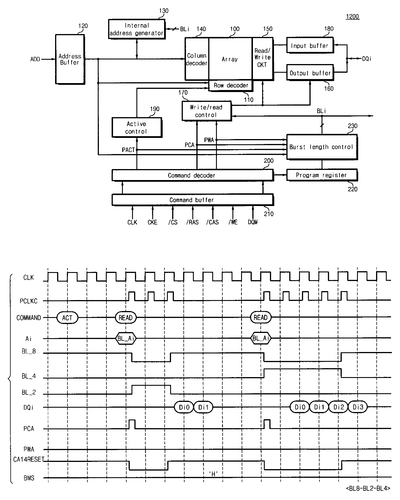
도 2은 본 발명에 따른 메모리 시스템을 개략적으로 보여주는 블록도이다. 도 2를 참조하면, 본 발명의 메모리 시스템 (1000)은 메모리 컨트롤러 (1100)와 반도체 메모리 장치 (1200)를 포함한다. 메모리 컨트롤러 (1100)는 파워-업시 반도체 메모리 장치 (1200)의 동작 모드를 설정한다. 그 다음에, 메모리 컨트롤러 (1100)는 버스트 읽기/쓰기 동작을 수행하도록 반도체 메모리 장치 (1200)로 액티브 명령 및 읽기/쓰기 명령을 순차적으로 출력한다. 특히, 메모리 컨트롤러 (1100)는 액티브 명령 또는 읽기/쓰기 명령과 함께 버스트 길이 정보를 반도체 메모리 장치 (1200)에 제공한다. 반도체 메모리 장치 (1200)는 메모리 컨트롤러 (1100)로부터의 버스트 길이 정보에 따라 출력/입력될 데이터의 버스트 길이를 내부적으로 설정한다. 본 발명에 따른 반도체 메모리 장치 (1200)는 읽기/쓰기 명령 또는 액티브 명령와 함께 입력되는 버스트 길이 정보 (예를 들면, 어드레스 정보)에 따라 동작 모드의 재설정없이 연속적으로 입/출력되는 데이터의 버스트 길이를 내부적으로 설정하며, 그렇게 설정된 버스트 길이에 따라 버스트 읽기/쓰기 동작을 수행한다. 게다가, 본 발명에 따른 반도체 메모리 장치 (1200)는 동작 모드를 설정할 때 결정된 버스트 길이에 따라 버스트 읽기/쓰기 동작을 수행할 수도 있다. 이러한 제어 방식에 따르면, 추가적인/번거로운 절차없이 버스트 길이를 가변시키는 것이 가능하다.2 is a block diagram schematically illustrating a memory system according to the present invention. Referring to FIG. 2, the
도 3은 본 발명의 바람직한 실시예에 따른 도 2에 도시된 반도체 메모리 장치를 개략적으로 보여주는 블록도이다. 도 3을 참조하면, 본 발명에 따른 반도체 메모리 장치는 동기형 DRAM이다. 하지만, 본 발명이 동기형 DRAM에 국한되지 않음은 자명하다.3 is a block diagram schematically illustrating the semiconductor memory device shown in FIG. 2 in accordance with a preferred embodiment of the present invention. Referring to FIG. 3, the semiconductor memory device according to the present invention is a synchronous DRAM. However, it is obvious that the present invention is not limited to synchronous DRAMs.
본 발명에 따른 반도체 메모리 장치 (1200)는 메모리 셀들이 행들과 열들로 배열된 메모리 셀 어레이 (memory cell array) (100)를 포함한다. 행 디코더 회로 (110)는 액티브 제어 회로 (active controller circuit) (190)에 의해서 제어되며, 어드레스 버퍼 회로 (address buffer circuit) (120)를 통해 입력된 행 어드레스에 응답하여 메모리 셀 어레이 (100)의 행들을 선택한다. 어드레스 버퍼 회로 (120)를 통해 입력된 열 어드레스는 내부 어드레스 발생 회로 (internal address generator circuit) (130) 및 열 디코더 회로 (column decoder circuit) (140)로 전달된다. 내부 어드레스 발생 회로 (130)는 버스트 길이 신호들 (BLi, i=1, 2, 4, 8, ...)에 응답하여 입력된 열 어드레스를 순차적으로 증가/감소시킨다. 즉, 내부 어드레스 발생 회로 (130)는 결정된 버스트 길이만큼 내부 열 어드레스들을 순차적으로 발생한다. 열 디코더 회로 (140)는 내부 어드레스 발생 회로 (130) (또는 어드레스 버퍼 회로)로부터의 열 어드레스에 응답하여 메모리 셀 어레이 (100)의 열들을 선택한다.The
읽기/쓰기 회로 (read/write circuit) (150)는, 버스트 읽기 동작시, 읽기/쓰기 제어 회로 (read/write controller circuit) (170)의 제어에 따라 선택된 열들의 메모리 셀들로부터 데이터를 읽고, 그렇게 읽혀진 데이터를 데이터 출력 버퍼 회로 (output buffer circuit) (160)를 통해 외부로 출력한다. 읽기/쓰기 회로 (150)는, 버스트 쓰기 동작시, 읽기/쓰기 제어 회로 (170)의 제어에 따라 입력 버퍼 회로 (input buffer circuit) (180)를 통해 입력된 데이터를 선택된 열들의 메모리 셀들에 저장한다. 읽기/쓰기 제어 회로 (170)는 쓰기 및 읽기 명령 신호들 (PWA, PCA) 및 버스트 길이 신호들 (BLi)에 응답하여 읽기/쓰기 회로 (150) 및 출력 버퍼 회로 (160)를 제어한다. 예를 들면, 읽기/쓰기 제어 회로 (170)는 활성화된 버스트 길이 신호에 의해서 결정된 버스트 길이만큼 데이터가 입/출력되도록 읽기/쓰기 회로 (150) 및 출력 버퍼 회로 (160)를 제어한다.Read /
계속해서 도 3을 참조하면, 명령 디코더 회로 (command decoder circuit) (200)는 정상적인 동작 모드에서 명령 버퍼 회로 (command buffer circuit) (210)를 통해 입력되는 제어 신호들에 응답하여 액티브 명령 신호 (PACT), 읽기 명령 신호 (PCA), 그리고 쓰기 명령 신호 (PWA)를 발생한다. 명령 디코더 회로 (200)는 동 작 모드를 설정하는 구간에서 메모리 장치의 동작 모드들 (예를 들면, 버스트 길이, 버스트 형태, CAS latency, 버스트 모드 정보, 등)을 프로그램하도록 프로그램 레지스터 (220)를 제어한다. 프로그램 레지스터 (220)에 저장된 동작 모드들에 있어서, 버스트 모드 정보는 반도체 메모리 장치 (1200)가 가변 버스트 모드 (variable burst mode)에서 또는 고정 버스트 모드 (fixed burst mode)에서 동작할 지의 여부를 나타낸다. 버스트 길이 제어 회로 (bufer length controller circuit) (230)는 명령 디코더 회로 (200)로부터의 명령 신호들 (PACT, PCA, PWA)에 응답하여 동작하며, 프로그램 레지스터 (220)에 저장된 버스트 길이 값 또는 어드레스 버퍼 회로 (120)를 통해 입력되는 버스트 어드레스에 따라 버스트 길이 신호들 (BLi) 중 하나를 활성화시킨다.3, the
여기서, 반도체 메모리 장치 (1200)가 고정 버스트 모드로 설정될 때, 반도체 메모리 장치 (1200)는 프로그램 레지스터 (220)에 저장된 고정 버스트 길이에 따라 버스트 읽기/쓰기 동작을 수행한다. 반도체 메모리 장치 (1200)가 가변 버스트 모드로 설정될 때, 반도체 메모리 장치 (1200)는 프로그램 레지스터 (220)에 저장된 고정 버스트 길이 뿐만 아니라 명령 (예를 들면, 액티브 명령, 쓰기 명령 또는 읽기 명령)와 함께 입력되는 외부 신호 (예를 들면, 어드레스)에 의해서 결정되는 버스트 길이에 따라 버스트 읽기/쓰기 동작을 수행하며, 이는 이후 상세히 설명될 것이다.Here, when the
도 4는 본 발명의 바람직한 실시예에 따른 도 3에 도시된 버스트 길이 제어 회로를 보여주는 블록도이다.4 is a block diagram showing the burst length control circuit shown in FIG. 3 according to a preferred embodiment of the present invention.
도 4를 참조하면, 버스트 길이 제어 회로 (230)는 프로그램 레지스터 (220)에 저장된 버스트 모드 신호 (BMS)에 따라 동작한다. 예를 들면, 버스트 모드 신호 (BMS)가 고정 버스트 모드를 나타낼 때, 버스트 길이 제어 회로 (230)는 프로그램 레지스터 (220)에 저장된 버스트 길이 값에 따라 버스트 길이 신호들 (BLi) 중 하나를 활성화시킨다. 이에 반해서, 버스트 모드 신호 (BMS)가 가변 버스트 모드를 나타낼 때, 버스트 길이 제어 회로 (230)는 어드레스 버퍼 회로 (120)로부터 출력되는 어드레스 정보에 따라 버스트 길이 신호들 (BLi) 중 하나를 활성화시킨다.Referring to FIG. 4, the burst
버스트 길이 제어 회로 (230)는 래치 회로 (latch circuit) (231), 제 1 및 제 2 디코더 회로들 (first and second decoder circuits) (232, 233), 스위치 제어 회로 (switch controller circuit) (234), 선택 회로 (selector circuit) (235), 그리고 신호 발생 회로 (signal generator circuit) (236)를 포함한다.The burst
먼저, 래치 회로 (231)는 가변 버스트 모드시 (또는 버스트 모드 신호 (BMS)가 하이로 활성화될 때) 액티브/읽기/쓰기 명령의 입력에 따라 어드레스 버퍼 회로 (120)의 출력을 래치한다. 제 1 디코더 회로 (232)는 래치 회로 (231)의 출력을 디코딩하고, 제 2 디코더 회로 (233)는 프로그램 레지스터 (220)로부터의 버스트 길이 데이터를 디코딩한다. 선택 회로 (235)는 스위치 제어 회로 (234)의 제어에 따라 제 1 디코더 회로 (232)의 디코딩 신호들 또는 제 2 디코더 회로 (233)의 디코딩 신호들을 선택한다. 신호 발생 회로 (236)는 선택 회로 (235)에 의해서 선택된 신호들에 응답하여 버스트 길이 신호들 (BLi) 중 어느 하나를 활성화시킨다.First, the
도 5a 및 도 5b는 본 발명의 바람직한 실시예에 따른 도 4에 도시된 버스트 길이 제어 회로를 보여주는 회로도들이다. 먼저, 도 5a를 참조하면, 래치 회로 (231)는 NOR 게이트들 (G1, G3), NAND 게이트들 (G2, G4, G5, G6), 각각이 2개의 인버터들로 구성된 래치들 (LAT1, LAT2, LAT3, LAT4, LAT5), 인버터들 (INV1, INV4, INV11, INV12, INV15, INV16), NMOS 트랜지스터들 (M1, M2), 그리고 전달 게이트들 (TG1, TG2, TG3, TG4, TG5)을 포함하며, 도면에 도시된 바와 같이 연결된다. 제어 신호 (BMS)는 프로그램 레지스터 (220)로부터 출력되는 버스트 모드 정보 (가변 버스트 모드 또는 고정 버스트 모드)를 나타낸다. 제어 신호 (PVCCH)는 파워-업시 활성화되는 펄스 신호이다. 제어 신호 (PVCCH)가 파워-업시 활성화될 때, 래치들 (LAT4, LAT5)은 초기화된다. 읽기 명령 신호 (PCA) 및 쓰기 명령 신호 (PWA)가 모두 로우 레벨로 유지될 때, 전달 게이트들 (TG4, TG5)은 도전되지 않는 반면에 전달 게이트들 (TG1-TG3)은 클록 신호 (PCLKC)의 하이 구간 동안 도전된다.5A and 5B are circuit diagrams showing the burst length control circuit shown in FIG. 4 according to a preferred embodiment of the present invention. First, referring to FIG. 5A, the
이러한 조건에 따르면, 제어 신호 (BMS)가 로우로 비활성화되는 경우 (또는 제어 신호 (BMS)가 고정 버스트 모드를 나타내는 경우), NAND 게이트들 (G4, G5, G6)의 출력들은 어드레스 버퍼 회로 (120)로부터의 어드레스 신호들 (TCA11, TCA12, TCA13)에 관계없이 하이 레벨로 유지된다. 즉, 제어 신호 (BMS)가 비활성화되는 경우 (또는 제어 신호 (BMS)가 고정 버스트 모드를 나타내는 경우), 래치 회로 (231)는 어드레스 버퍼 회로 (120)로부터의 어드레스 신호들 (TCA11, TCA12, TCA13)을 래치하지 않는다. 이에 반해서, 제어 신호 (BMS)가 하이로 활성화되는 경우 (또는 제어 신호 (BMS)가 가변 버스트 모드를 나타내는 경우), 어드레스 버퍼 회로 (120)로부터의 어드레스 신호들 (TCA11, TCA12, TCA13)은 읽기 명령 신호 (PCA) 또는 쓰기 명령 신호 (PWA)가 활성화되는 동안 대응하는 전달 게이트들 (TG1, TG2, TG3)을 통해 대응하는 래치들 (LAT1, LAT2, LAT3)에 각각 래치된다. 그 다음에, 래치들 (LAT2, LAT3)에 래치된 값들은 전달 게이트들 (TG4, TG5)을 통해 래치들 (LAT4, LAT5)로 각각 전달된다. 전달 게이트들 (TG4, TG5)은 읽기 또는 쓰기 명령 신호 (PCA 또는 PWA)가 비활성화된 후 도전되지 않는다. 즉, 래치들 (LAT4, LAT5)에 저장된 값들은 다음의 읽기 또는 쓰기 명령이 입력되기 이전까지 변화되지 않는다.According to this condition, when the control signal BMS is deactivated low (or when the control signal BMS indicates the fixed burst mode), the outputs of the NAND gates G4, G5, and G6 are the
요약하면, 래치 회로 (231)는 반도체 메모리 장치 (1200)가 가변 버스트 모드로 설정되고 읽기 명령 신호 (PCA) 또는 쓰기 명령 신호 (PWA)가 활성화될 때마다 어드레스 버퍼 회로 (120)로부터 출력되는 어드레스 신호들 (TCA11, TCA12, TCA13)을 래치한다.In summary, the
도 5b를 참조하면, 제 1 디코더 회로 (232)는 인버터들 (INV17, INV18)과 NAND 게이트들 (G7, G8, G9, G10)을 포함하며, 도면에 도시된 바와 같이 연결되어 있다. 제 1 디코더 회로 (232)는 래치 회로 (231)로부터 출력되는 어드레스 신호들 (CA12_BL, CA13_BL)을 디코딩한다. 제 2 디코더 회로 (233)는 인버터들 (INV19, INV20, INV21)과 NAND 게이트들 (G11, G12, G13, G14)을 포함하며, 도면에 도시된 바와 같이 연결되어 있다. 제 2 디코더 회로 (233)는 프로그램 레지스터 (220)로부터 출력되는 신호들 (MDST0, MDST1, MDST2)을 디코딩한다. 여기서, 제 1 디코더 회로(232)에 입력되는 신호들 (CA12_BL, CA13_BL)은 정상 동작 모드에서 명령와 함께 입력된 신호들인 반면에, 제 2 디코더 회로(233)에 입력되는 신호들 (MDST0-MDST2)은 동작 모드 설정 구간 동안 입력된 신호들이다.Referring to FIG. 5B, the
계속해서 도 5b를 참조하면, 스위치 제어 회로 (234)는 NOR 게이트 (G15), NAND 게이트들 (G16, G17, G18), 그리고 인버터들 (INV22, INV23, INV24)을 포함하며, 도면에 도시된 바와 같이 연결되어 있다. 스위치 제어 회로 (234)는 제어 신호들 (PCA, PWA, BMS, CA11_BL, CA14RESET)에 응답하여 선택 신호들 (S1, S1B, S2, S2B)을 발생한다. 여기서, 제어 신호 (CA14RESET)는 메모리 장치가 가변 버스트 모드로 설정될 때 초기에 설정된 버스트 길이 값에 의해서 버스트 길이 신호가 활성화되도록 하는 데 사용된다. 예를 들면, 내부 어드레스 발생 회로 (130)가 설정된 버스트 길이만큼 내부 어드레스를 발생한 후 제어 신호 (CA14RSET)가 펄스 형태로 활성화된다. 선택 회로 (235)는 전달 게이트들 (TG6-TG13)로 구성되며, 선택 신호들 (S1, S1B, S2, S2B)에 응답하여 제 1 디코더 회로 (232)의 출력 신호들 또는 제 2 디코더 회로 (233)의 출력 신호들을 선택한다.With continued reference to FIG. 5B, the
제어 신호 (BMS)가 비활성화되는 경우 (또는 제어 신호 (BMS)가 고정 버스트 모드를 나타내는 경우), 선택 신호들 (S1, S1B)은 각각 로우 레벨과 하이 레벨이 되고 선택 신호들 (S2, S2B)은 각각 하이 레벨과 로우 레벨이 된다. 이는 전달 게이트들 (TG6, TG8, TG10, TG12)이 도전되게 한다. 즉, 선택 회로 (235)는 제 2 디코더 회로 (233)의 출력 신호들을 선택한다. 제어 신호 (BMS)가 고정 버스트 모드를 나타낼 때, 읽기 명령 신호 (PCA), 쓰기 명령 신호 (PWA) 및 어드레스 신호 (CA11_BL)에 관계없이 프로그램 레지스터 (220)에 저장된 버스트 길이 값에 의해서 버스트 길이가 결정된다.When the control signal BMS is deactivated (or when the control signal BMS indicates the fixed burst mode), the selection signals S1 and S1B become the low level and the high level, respectively, and the selection signals S2 and S2B Are the high level and the low level, respectively. This causes the transfer gates TG6, TG8, TG10, TG12 to be conductive. That is, the
제어 신호 (BMS)가 활성화되는 경우 (또는 제어 신호 (BMS)가 가변 버스트 모드를 나타내는 경우), 선택 신호들 (S1, S1B, S2, S2B)의 로직 상태들은 어드레스 신호 (CA11_BL), 읽기 명령 신호 (PCA), 쓰기 명령 신호 (PWA), 그리고 제어 신호 (CA14RESET)에 의해서 결정된다. 구체적으로, 어드레스 신호 (CA11_BL)가 하이로 유지되는 경우, 선택 신호들 (S1, S1B)은 읽기 명령 신호 (PCA) 또는 쓰기 명령 신호 (PWA)가 하이로 활성화될 때 각각 하이 레벨과 로우 레벨이 된다. 이는 전달 게이트들 (TG7, TG9, TG11, TG13)이 도전되게 한다. 즉, 제 1 디코더 회로 (232)의 출력 신호들이 신호 발생 회로 (236)로 전달된다. 활성화된 읽기/쓰기 명령 신호 (PCA/PWA)가 비활성화됨에 따라, 선택 신호들 (S1, S1B)은 각각 로우 레벨과 하이 레벨이 된다. 이는 전달 게이트들 (TG7, TG9, TG11, TG13)이 비도전되게 한다. 선택 신호 (S1B)가 하이 레벨이고 제어 신호 (CA14RESET)가 로우 레벨에서 하이 레벨로 천이할 때, 선택 신호들 (S2, S2B)은 각각 하이 레벨과 로우 레벨이 된다. 이는 전달 게이트들 (TG6, TG8, TG10, TG12)이 도전되게 한다. 즉, 제 2 디코더 회로 (233)의 출력 신호들이 신호 발생 회로 (236)로 전달된다. 다시말해서, 가변 버스트 모드에서 외부 어드레스에 의해서 버스트 길이 신호들이 선택적으로 활성화된 후, 버스트 길이 신호들은 프로그램 레지스터 (220)에 저장된 버스트 길이 값에 의해서 초기화된다. 이는 읽기/쓰기 명령과 함께 외부 어드레스 (버스트 길이를 가변시키기 위한 어드레스)가 입력되지 않더라도 버스트 읽기/쓰기 동작이 프로그램 레지스터 (220)에 저장된 버스트 길이 값을 이용하여 수행됨을 의미한다.When the control signal BMS is activated (or when the control signal BMS indicates the variable burst mode), the logic states of the selection signals S1, S1B, S2, S2B are the address signal CA11_BL, the read command signal. (PCA), write command signal (PWA), and control signal (CA14RESET). Specifically, when the address signal CA11_BL is kept high, the selection signals S1 and S1B have a high level and a low level, respectively, when the read command signal PCA or the write command signal PWA is activated high. do. This causes the transfer gates TG7, TG9, TG11, TG13 to be conductive. That is, output signals of the
계속해서 도 5b를 참조하면, 신호 발생 회로 (236)는 래치들 (LAT6, LAT7, LAT8, LAT9), NAND 게이트들 (G19, G22), NOR 게이트들 (G20, G21, G23, G24), 그 리고 인버터들 (INV25, INV26, INV27, INV30, INV35)을 포함하며, 도면에 도시된 바와 같이 연결되어 있다. 신호 발생 회로 (236)는 선택 회로 (235)에 의해서 선택된 신호들에 응답하여 버스트 길이 신호들 (BLi) (이 실시예에 있어서, i=1, 2, 4, 8, 16, FULL) 중 하나를 활성화시킨다.With continued reference to FIG. 5B,
도 6은 본 발명에 따른 반도체 메모리 장치의 버스트 읽기 동작을 설명하기 위한 타이밍도이다. 본 발명에 따른 반도체 메모리 장치의 동작이 참조 도면들에 의거하여 이하 상세히 설명될 것이다. 본 발명에 따른 버스트 읽기 동작을 설명하기에 앞서, 버스트 길이가 8로 설정되고 버스트 모드 신호 (BMS)가 가변 버스트 모드를 나타내도록 프로그램 레지스터 (220)가 프로그램되었다고 가정하자.6 is a timing diagram illustrating a burst read operation of the semiconductor memory device according to the present invention. The operation of the semiconductor memory device according to the present invention will be described in detail below with reference to the accompanying drawings. Prior to describing the burst read operation according to the present invention, assume that the
버스트 읽기 동작은 액티브 명령 (ACT)와 읽기 명령 (READ)이 정해진 타이밍에 따라 메모리 장치 (1200)에 입력될 때 수행된다. 잘 알려진 바와 같이, 읽기 명령 (READ)이 입력될 때 열 어드레스가 어드레스 버퍼 회로 (120)에 제공된다. 본 발명에 따르면, 읽기 명령과 함께 입력되는 열 어드레스는 버스트 어드레스 (BL_Ai) (이 실시예에서, i=11, 12, 13)를 포함한다. 어드레스 버퍼 회로 (120)에 입력된 버스트 어드레스 (TCAi)는 버스트 길이 제어 회로 (230)로 전달된다. 버스트 길이 제어 회로 (230)의 래치 회로 (231)는 읽기 명령 신호 (PCA)이 하이로 활성화될 때 버스트 어드레스 신호들 (TCA11, TCA12, TCA13)을 래치한다. 이때, 버스트 어드레스 신호 (TCA11)가 하이 레벨을 갖는다고 가정하자. 래치 회로 (231)에서 출력된 버스트 어드레스 신호들 (CA12_BL, CA13_BL)은 제 1 디코더 회로 (232)에 의해서 디코딩된다.The burst read operation is performed when the active command ACT and the read command READ are input to the
스위치 제어 회로 (235)는 읽기 명령 신호 (PCA)의 활성화에 응답하여 하이 레벨의 선택 신호 (S1)과 로우 레벨의 선택 신호 (S1B)를 출력한다. 이에 따라, 전달 게이트들 (TG7, TG9, TG11, TG13)이 도전되어 제 1 디코더 회로 (232)의 출력 신호들은 신호 발생 회로 (236)로 전달된다. 이때, 선택 신호들 (S2, S2B)은 로우 레벨과 하이 레벨을 갖는다. 신호 발생 회로 (236)는 제 1 디코더 회로 (232)의 출력 신호들에 응답하여 버스트 길이 신호들 (BL1, BL2, BL4, BL8, BL16) 중 하나 (예를 들면, BL2)를 활성화시킨다. 이후, 내부 어드레스 발생 회로 (130)는 활성화된 버스트 길이 신호에 응답하여 내부 어드레스들을 순차적으로 생성한다. 그리고, 읽기/쓰기 제어 회로 (170)는 설정된 버스트 길이만큼 데이터가 연속적으로 출력되도록 활성화된 버스트 길이 신호에 응답하여 읽기/쓰기 회로 (150) 및 출력 버퍼 회로 (160)를 제어한다.The
도 6에 도시된 바와 같이, 제어 신호 (CA14RESET)가 로우 레벨에서 하이 레벨로 천이함에 따라, 선택 신호 (S2)는 로우 레벨에서 하이 레벨로 천이하고 선택 신호 (S2B)은 하이 레벨에서 로우 레벨로 천이한다. 이는 전달 게이트들 (TG6, TG8, TG10, TG12)이 도전되게 하며, 그 결과 제 2 디코더 회로 (233)의 출력 신호들이 신호 발생 회로 (236)로 전달된다. 즉, 반도체 메모리 장치 (1200)는 초기에 설정된 버스트 길이를 갖는다. 다음의 버스트 읽기/쓰기 동작에서 외부에서 버스트 어드레스가 입력되지 않을 경우, 초기에 설정된 버스트 길이에 따라 버스트 읽기/쓰기 동작이 수행될 것이다. 도 7에 도시된 바와 같이, 만약 버스트 길이 신호 (BL_4)를 선택하기 위한 버스트 어드레스 (BL_Ai)와 함께 읽기 명령이 다시 입력되 면, 버스트 길이 신호 (BL_8)는 비활성화되는 반면에 버스트 길이 신호 (BL_4)가 앞서 설명된 것과 동일한 방법으로 활성화되며, 그것에 대한 설명은 그러므로 생략된다.As shown in Fig. 6, as the control signal CA14RESET transitions from the low level to the high level, the select signal S2 transitions from the low level to the high level and the select signal S2B goes from the high level to the low level. Transition This causes the transfer gates TG6, TG8, TG10, TG12 to be conductive so that the output signals of the
비록 읽기 명령들이 연속적으로 입력되었지만, 읽기 명령 다음에 버스트 어드레스와 함께 쓰기 명령이 입력될 수 있음은 자명하다. 이때, 읽기 명령 신호 (PCA) 대신에 쓰기 명령 신호 (PWA)가 활성화된다는 점을 제외하면, 버스트 쓰기 동작에서의 버스트 길이 제어 스킴은 앞서 설명도니 버스트 읽기 동작의 그것과 동일하다.Although read commands have been entered in succession, it is obvious that a write command may be entered with a burst address following the read command. At this time, except that the write command signal PWA is activated instead of the read command signal PCA, the burst length control scheme in the burst write operation is the same as that of the burst read operation described above.
도 7은 본 발명에 따른 반도체 메모리 장치의 다른 버스트 읽기 동작을 설명하기 위한 타이밍도이다. 도 7에서 알 수 있듯이, 버스트 어드레스가 읽기/쓰기 명령와 함께 입력되는 것이 아니라 액티브 명령과 함께 입력된다. 이러한 경우, 도 5b의 스위치 제어 회로 (234)의 NOR 게이트 (G15)는 읽기 명령 신호, 쓰기 명령 신호 그리고 액티브 명령 신호를 받아들이도록 구성될 것이다. 이러한 점을 제외하면 도 7의 버스트 읽기/쓰기 동작은 도 6에서 설명된 버스트 읽기/쓰기 동작과 동일하며, 그것에 대한 설명은 그러므로 생략될 것이다.7 is a timing diagram illustrating another burst read operation of the semiconductor memory device according to the present invention. As can be seen in FIG. 7, the burst address is input with the active command rather than with the read / write command. In this case, the NOR gate G15 of the
비록 본 발명에 따른 반도체 메모리 장치의 버스트 길이가 동작 모드의 재설정없이 가변되었지만, 본 발명이 이에 국한되지 않음은 자명하다. 예를 들면, 본 발명에 따른 반도체 메모리 장치는 CAS 레이턴시 (또는 프로그램 레지스터에 프로그램되는 모든 동작 모드들)가 읽기/쓰기 명령과 함께 입력된 외부 신호에 의해서 가변되도록 구성될 수 있다. 이상에서, 본 발명에 따른 회로의 구성 및 동작을 상 기한 설명 및 도면에 따라 도시하였지만, 이는 예를 들어 설명한 것에 불과하며 본 발명의 기술적 사상 및 범위를 벗어나지 않는 범위 내에서 다양한 변화 및 변경이 가능함은 물론이다.Although the burst length of the semiconductor memory device according to the present invention is varied without resetting the operation mode, it is obvious that the present invention is not limited thereto. For example, the semiconductor memory device according to the present invention may be configured such that the CAS latency (or all operation modes programmed in the program register) is varied by an external signal input with a read / write command. In the above, the configuration and operation of the circuit according to the present invention are shown according to the above description and drawings, but this is merely described for example, and various changes and modifications are possible within the scope without departing from the spirit and scope of the present invention. Of course.
상술한 바와같이, 동작 모드의 재설정없이 액티브/읽기/쓰기 명령와 입력되는 외부 신호 (예를 들면, 어드레스)에 의해서 버스트 길이를 가변시킬 수 있다.As described above, the burst length can be changed by an active / read / write command and an external signal (for example, an address) inputted without resetting the operation mode.
Claims (20)
Priority Applications (6)
| Application Number | Priority Date | Filing Date | Title |
|---|---|---|---|
| KR1020030070311A KR100560773B1 (en) | 2003-10-09 | 2003-10-09 | Semiconductor memory device capable of controlling burst length without resetting the operating mode and memory system comprising the same |
| US10/951,881 US7042800B2 (en) | 2003-10-09 | 2004-09-29 | Method and memory system in which operating mode is set using address signal |
| DE102004050037.1A DE102004050037B4 (en) | 2003-10-09 | 2004-10-07 | Memory device, memory system and mode of operation network method |
| TW093130620A TWI258143B (en) | 2003-10-09 | 2004-10-08 | Method and memory system in which operating mode is set using address signal |
| CN2004100471843A CN1652248B (en) | 2003-10-09 | 2004-10-09 | Method and memory system in which operating mode is set using address signal |
| JP2004298003A JP2005116167A (en) | 2003-10-09 | 2004-10-12 | Memory system and method for setting operation mode by address signal |
Applications Claiming Priority (1)
| Application Number | Priority Date | Filing Date | Title |
|---|---|---|---|
| KR1020030070311A KR100560773B1 (en) | 2003-10-09 | 2003-10-09 | Semiconductor memory device capable of controlling burst length without resetting the operating mode and memory system comprising the same |
Publications (2)
| Publication Number | Publication Date |
|---|---|
| KR20050034402A KR20050034402A (en) | 2005-04-14 |
| KR100560773B1 true KR100560773B1 (en) | 2006-03-13 |
Family
ID=34420577
Family Applications (1)
| Application Number | Title | Priority Date | Filing Date |
|---|---|---|---|
| KR1020030070311A Expired - Fee Related KR100560773B1 (en) | 2003-10-09 | 2003-10-09 | Semiconductor memory device capable of controlling burst length without resetting the operating mode and memory system comprising the same |
Country Status (2)
| Country | Link |
|---|---|
| US (1) | US7042800B2 (en) |
| KR (1) | KR100560773B1 (en) |
Families Citing this family (12)
| Publication number | Priority date | Publication date | Assignee | Title |
|---|---|---|---|---|
| KR100546339B1 (en) | 2003-07-04 | 2006-01-26 | 삼성전자주식회사 | Semiconductor device capable of selectively implementing a single data strobe mode with a differential data strobe mode and a data inversion scheme |
| KR100618704B1 (en) * | 2004-12-20 | 2006-09-08 | 주식회사 하이닉스반도체 | How to control MRS setting operation of a memory device |
| US8731562B2 (en) | 2005-08-30 | 2014-05-20 | Telefonaktiebolaget L M Ericsson (Publ) | Detection of control messages for HSDPA |
| KR100902048B1 (en) * | 2007-05-14 | 2009-06-15 | 주식회사 하이닉스반도체 | Address Receiving Circuit of Semiconductor Device |
| KR100857450B1 (en) * | 2007-08-10 | 2008-09-10 | 주식회사 하이닉스반도체 | Output Enable Signal Generation Circuit and Method of Semiconductor Memory Device |
| US7859937B2 (en) * | 2009-01-12 | 2010-12-28 | Arm Limited | Apparatus and method for controlling write access to a group of storage elements |
| US8677100B2 (en) * | 2009-07-17 | 2014-03-18 | Macronix International Co., Ltd. | Serial memory interface for extended address space |
| KR20120098325A (en) * | 2011-02-28 | 2012-09-05 | 에스케이하이닉스 주식회사 | Non-volatile memory system and setting method of feature |
| KR102135426B1 (en) * | 2013-12-10 | 2020-07-17 | 에스케이하이닉스 주식회사 | Operation mode setting circuit of semiconductor apparatus and data processing system using the same |
| KR102164019B1 (en) * | 2014-01-27 | 2020-10-12 | 에스케이하이닉스 주식회사 | Burst Length control device and semiconductor device including the same |
| US10534540B2 (en) * | 2016-06-06 | 2020-01-14 | Micron Technology, Inc. | Memory protocol |
| KR102692011B1 (en) * | 2018-11-02 | 2024-08-05 | 에스케이하이닉스 주식회사 | Semiconductor device |
Family Cites Families (11)
| Publication number | Priority date | Publication date | Assignee | Title |
|---|---|---|---|---|
| JPH06267283A (en) | 1993-03-16 | 1994-09-22 | Mitsubishi Electric Corp | Read-only memory writable data and method for writing/ reading data |
| JPH06290582A (en) * | 1993-04-02 | 1994-10-18 | Nec Corp | Semiconductor memory |
| JPH07282580A (en) | 1994-04-13 | 1995-10-27 | Nec Commun Syst Ltd | DRAM power consumption reduction method |
| US5598376A (en) * | 1994-12-23 | 1997-01-28 | Micron Technology, Inc. | Distributed write data drivers for burst access memories |
| KR19980019814A (en) | 1996-09-03 | 1998-06-25 | 김광호 | Burst type memory with variable burst length |
| EP0929075B1 (en) * | 1996-09-26 | 2003-08-20 | Mitsubishi Denki Kabushiki Kaisha | Synchronous type semiconductor memory device |
| US6016066A (en) | 1998-03-19 | 2000-01-18 | Intel Corporation | Method and apparatus for glitch protection for input buffers in a source-synchronous environment |
| JP4011833B2 (en) * | 2000-06-30 | 2007-11-21 | 株式会社東芝 | Semiconductor memory |
| US6633951B2 (en) | 2001-03-15 | 2003-10-14 | Intel Corporation | Method for reducing power consumption through dynamic memory storage inversion |
| KR20030039179A (en) | 2001-11-12 | 2003-05-17 | 삼성전자주식회사 | Synchronous semiconductor memory apparatus capable of accomplishing mode change between single-ended strobe mode and differential strobe mode |
| KR100546339B1 (en) | 2003-07-04 | 2006-01-26 | 삼성전자주식회사 | Semiconductor device capable of selectively implementing a single data strobe mode with a differential data strobe mode and a data inversion scheme |
-
2003
- 2003-10-09 KR KR1020030070311A patent/KR100560773B1/en not_active Expired - Fee Related
-
2004
- 2004-09-29 US US10/951,881 patent/US7042800B2/en not_active Expired - Lifetime
Also Published As
| Publication number | Publication date |
|---|---|
| US7042800B2 (en) | 2006-05-09 |
| KR20050034402A (en) | 2005-04-14 |
| US20050078548A1 (en) | 2005-04-14 |
Similar Documents
| Publication | Publication Date | Title |
|---|---|---|
| JP4159280B2 (en) | Semiconductor memory device | |
| JP4287158B2 (en) | NAND flash memory device | |
| JPH01118297A (en) | Non-volatile semiconductor memory | |
| KR100560773B1 (en) | Semiconductor memory device capable of controlling burst length without resetting the operating mode and memory system comprising the same | |
| KR100902125B1 (en) | Dram for low power consumption and driving method thereof | |
| KR102466965B1 (en) | Semiconductor device | |
| US6930919B2 (en) | NAND-type flash memory device having array of status cells for storing block erase/program information | |
| JP4439033B2 (en) | Semiconductor memory device | |
| CN101022038A (en) | Burst read circuit in semiconductor memory device and burst data read method thereof | |
| KR100719377B1 (en) | Semiconductor memory device that reads data patterns | |
| JP2005116167A (en) | Memory system and method for setting operation mode by address signal | |
| JP5020489B2 (en) | Semiconductor memory device capable of changing the number of banks to be refreshed at the time of refreshing and its operating method | |
| US6377509B2 (en) | Semiconductor integrated circuit | |
| CN120452517A (en) | Rising edge detection for shut-down cycle of multi-cycle operation | |
| JP4327482B2 (en) | Synchronous semiconductor memory device | |
| JP2007200457A (en) | Nonvolatile semiconductor storage device | |
| KR100598907B1 (en) | Flash memory with continuous read / write | |
| CN101427319A (en) | Memories with Clocked Sense Amplifiers | |
| JPH0770213B2 (en) | Semiconductor memory device | |
| KR20020012800A (en) | Nonvolatile memory, system comprising a plurality of nonvolatile memorys, and data read method thereof | |
| TW202213668A (en) | Logic simulation device and logic simulation program | |
| JP4727241B2 (en) | Semiconductor memory device and data writing and reading method for the device | |
| JPH06275066A (en) | Single-clock memory provided with page mode | |
| JPH09180443A (en) | Semiconductor memory circuit | |
| JP2004206850A (en) | Semiconductor storage device |
Legal Events
| Date | Code | Title | Description |
|---|---|---|---|
| A201 | Request for examination | ||
| PA0109 | Patent application |
St.27 status event code: A-0-1-A10-A12-nap-PA0109 |
|
| PA0201 | Request for examination |
St.27 status event code: A-1-2-D10-D11-exm-PA0201 |
|
| R18-X000 | Changes to party contact information recorded |
St.27 status event code: A-3-3-R10-R18-oth-X000 |
|
| P11-X000 | Amendment of application requested |
St.27 status event code: A-2-2-P10-P11-nap-X000 |
|
| P13-X000 | Application amended |
St.27 status event code: A-2-2-P10-P13-nap-X000 |
|
| PG1501 | Laying open of application |
St.27 status event code: A-1-1-Q10-Q12-nap-PG1501 |
|
| E902 | Notification of reason for refusal | ||
| PE0902 | Notice of grounds for rejection |
St.27 status event code: A-1-2-D10-D21-exm-PE0902 |
|
| PN2301 | Change of applicant |
St.27 status event code: A-3-3-R10-R13-asn-PN2301 St.27 status event code: A-3-3-R10-R11-asn-PN2301 |
|
| T11-X000 | Administrative time limit extension requested |
St.27 status event code: U-3-3-T10-T11-oth-X000 |
|
| PN2301 | Change of applicant |
St.27 status event code: A-3-3-R10-R13-asn-PN2301 St.27 status event code: A-3-3-R10-R11-asn-PN2301 |
|
| E13-X000 | Pre-grant limitation requested |
St.27 status event code: A-2-3-E10-E13-lim-X000 |
|
| P11-X000 | Amendment of application requested |
St.27 status event code: A-2-2-P10-P11-nap-X000 |
|
| P13-X000 | Application amended |
St.27 status event code: A-2-2-P10-P13-nap-X000 |
|
| E701 | Decision to grant or registration of patent right | ||
| PE0701 | Decision of registration |
St.27 status event code: A-1-2-D10-D22-exm-PE0701 |
|
| GRNT | Written decision to grant | ||
| PR0701 | Registration of establishment |
St.27 status event code: A-2-4-F10-F11-exm-PR0701 |
|
| PR1002 | Payment of registration fee |
St.27 status event code: A-2-2-U10-U11-oth-PR1002 Fee payment year number: 1 |
|
| PG1601 | Publication of registration |
St.27 status event code: A-4-4-Q10-Q13-nap-PG1601 |
|
| PR1001 | Payment of annual fee |
St.27 status event code: A-4-4-U10-U11-oth-PR1001 Fee payment year number: 4 |
|
| PR1001 | Payment of annual fee |
St.27 status event code: A-4-4-U10-U11-oth-PR1001 Fee payment year number: 5 |
|
| PR1001 | Payment of annual fee |
St.27 status event code: A-4-4-U10-U11-oth-PR1001 Fee payment year number: 6 |
|
| PR1001 | Payment of annual fee |
St.27 status event code: A-4-4-U10-U11-oth-PR1001 Fee payment year number: 7 |
|
| R18-X000 | Changes to party contact information recorded |
St.27 status event code: A-5-5-R10-R18-oth-X000 |
|
| FPAY | Annual fee payment |
Payment date: 20130228 Year of fee payment: 8 |
|
| PR1001 | Payment of annual fee |
St.27 status event code: A-4-4-U10-U11-oth-PR1001 Fee payment year number: 8 |
|
| FPAY | Annual fee payment |
Payment date: 20140228 Year of fee payment: 9 |
|
| PR1001 | Payment of annual fee |
St.27 status event code: A-4-4-U10-U11-oth-PR1001 Fee payment year number: 9 |
|
| FPAY | Annual fee payment |
Payment date: 20150302 Year of fee payment: 10 |
|
| PR1001 | Payment of annual fee |
St.27 status event code: A-4-4-U10-U11-oth-PR1001 Fee payment year number: 10 |
|
| PR1001 | Payment of annual fee |
St.27 status event code: A-4-4-U10-U11-oth-PR1001 Fee payment year number: 11 |
|
| FPAY | Annual fee payment |
Payment date: 20170228 Year of fee payment: 12 |
|
| PR1001 | Payment of annual fee |
St.27 status event code: A-4-4-U10-U11-oth-PR1001 Fee payment year number: 12 |
|
| FPAY | Annual fee payment |
Payment date: 20180228 Year of fee payment: 13 |
|
| PR1001 | Payment of annual fee |
St.27 status event code: A-4-4-U10-U11-oth-PR1001 Fee payment year number: 13 |
|
| PR1001 | Payment of annual fee |
St.27 status event code: A-4-4-U10-U11-oth-PR1001 Fee payment year number: 14 |
|
| PR1001 | Payment of annual fee |
St.27 status event code: A-4-4-U10-U11-oth-PR1001 Fee payment year number: 15 |
|
| PR1001 | Payment of annual fee |
St.27 status event code: A-4-4-U10-U11-oth-PR1001 Fee payment year number: 16 |
|
| PR1001 | Payment of annual fee |
St.27 status event code: A-4-4-U10-U11-oth-PR1001 Fee payment year number: 17 |
|
| PC1903 | Unpaid annual fee |
St.27 status event code: A-4-4-U10-U13-oth-PC1903 Not in force date: 20230308 Payment event data comment text: Termination Category : DEFAULT_OF_REGISTRATION_FEE |
|
| PC1903 | Unpaid annual fee |
St.27 status event code: N-4-6-H10-H13-oth-PC1903 Ip right cessation event data comment text: Termination Category : DEFAULT_OF_REGISTRATION_FEE Not in force date: 20230308 |