KR100558692B1 - Semiconductor Integrated Circuit Manufacturing Method - Google Patents
Semiconductor Integrated Circuit Manufacturing Method Download PDFInfo
- Publication number
- KR100558692B1 KR100558692B1 KR1020020076028A KR20020076028A KR100558692B1 KR 100558692 B1 KR100558692 B1 KR 100558692B1 KR 1020020076028 A KR1020020076028 A KR 1020020076028A KR 20020076028 A KR20020076028 A KR 20020076028A KR 100558692 B1 KR100558692 B1 KR 100558692B1
- Authority
- KR
- South Korea
- Prior art keywords
- electric field
- polishing
- copper
- insulating film
- forming
- Prior art date
- Legal status (The legal status is an assumption and is not a legal conclusion. Google has not performed a legal analysis and makes no representation as to the accuracy of the status listed.)
- Expired - Fee Related
Links
Images


Classifications
-
- H10P52/403—
-
- H10W20/062—
Landscapes
- Mechanical Treatment Of Semiconductor (AREA)
Abstract
반도체 집적회로의 제조방법이 개시된다.A method for manufacturing a semiconductor integrated circuit is disclosed.
본 발명에 따른 반도체 집적회로의 제조방법은 기판 상에 형성된 절연막에 배선을 형성하기 위한 배선용 홈을 형성하는 단계; 상기 배선용 홈을 매입하도록, 상기 절연막 상에 구리층을 형성하는 단계; 및 pH 7∼12의 슬러리를 사용하고, 연마패드와 상기 구리층 사이에 -4 ∼ -1kV/m 또는 1 ∼ 4kV/m의 DC 전기장을 인가하며 화학적 기계적 연마하는 단계를 포함하며, 본 발명에 따르면 Cu 및 SiO2의 연마 선택비를 조절함으로써 디싱 발생을 최소화하여 평탄화를 향상시킬 수 있다. A method for manufacturing a semiconductor integrated circuit according to the present invention includes the steps of forming a groove for wiring for forming a wiring in an insulating film formed on a substrate; Forming a copper layer on the insulating film to fill the wiring groove; And chemical mechanical polishing using a slurry of pH 7-12, applying a DC electric field of -4 to -1 kV / m or 1 to 4 kV / m between the polishing pad and the copper layer. According to this, by adjusting the polishing selectivity of Cu and SiO 2 it is possible to minimize the dishing to improve the planarization.
전기장, 화학적 기계적 연마, 평탄화, 디싱,Electric field, chemical mechanical polishing, planarization, dishing,
Description
도 1은 디싱이 발생하는 메커니즘의 개략도이다.1 is a schematic of the mechanism by which dishing occurs.
도 2는 본 발명의 바람직한 일 실시예에 따라, 연마공정 이전에 구리층까지 적층된 상태의 단면도를 나타낸다.Figure 2 shows a cross-sectional view of the laminated state to the copper layer prior to the polishing process, according to an embodiment of the present invention.
도 3은 본 발명에 따른 화학적 기계적 연마시스템에 대한 개략도이다.3 is a schematic diagram of a chemical mechanical polishing system according to the present invention.
도 4는 Pourbaix 다이아그램을 나타낸다.4 shows a Pourbaix diagram.
도 5는 본 발명에 따라 전기장을 인가하며 화학적 기계적 연마를 하는 개략도를 나타낸다.5 shows a schematic view of applying an electric field and performing chemical mechanical polishing according to the present invention.
도 6은 실시예 1∼4 및 33∼36과 비교예 1 및 9에 있어서, 인가되는 전기장의 세기에 따른 CuO와 Cu의 상대인 인텐시티의 변화를 나타낸다.FIG. 6 shows the changes in the intensities of CuO and Cu relative to the intensity of the electric field applied in Examples 1 to 4 and 33 to 36 and Comparative Examples 1 and 9. FIG.
도 7은 실시예 1∼4 및 29∼32와 비교예 1 및 8에 있어서 인가되는 전기장의 세기에 따른 Cu의 연마속도의 변화를 나타낸다.Fig. 7 shows changes in the polishing rate of Cu depending on the intensity of the electric field applied in Examples 1 to 4 and 29 to 32 and Comparative Examples 1 and 8.
도 8는 실시예 1∼4 및 비교예 1에 있어서, 인가되는 전기장의 세기에 따른 Cu 및 SiO2의 연마속도와 선택도의 변화를 나타낸다.FIG. 8 shows changes in the polishing rate and selectivity of Cu and SiO 2 according to the intensity of the electric field applied in Examples 1 to 4 and Comparative Example 1. FIG.
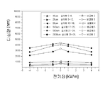
도 9은 실시예 5∼28 및 비교예 2∼7에 있어서, 선폭의 변화 및 인가되는 전 기장의 세기에 따른 디싱량의 변화를 나타낸다.9 shows Examples 5 to 28 and Comparative Examples 2 to 7 showing changes in line width and change in dishing amount according to the intensity of the applied electric field.
도 10은 본 발명에 따라 전기장이 인가됨에 의해 디싱이 감소되는 것을 확인할 수 있는 SEM사진이다. 10 is a SEM photograph to confirm that dishing is reduced by applying an electric field according to the present invention.
<도면의 주요부분에 대한 부호의 설명><Description of the symbols for the main parts of the drawings>
1: 샘플 캐리어 2: 전극1: sample carrier 2: electrode
3: 샘플 웨이퍼 4: 연마 슬러리3: sample wafer 4: polishing slurry
5: 연마 패드 6: 연마 플레이트5: polishing pad 6: polishing plate
7: 슬러리 공급장치 7: slurry feeder
본 발명은 반도체 회로의 제조방법에 관한 것으로서, 더욱 상세하게는 화학적 기계적 연마(Chemical Mechanical Polishing:CMP)시 구리 배선(패턴)의 디싱을 감소시키는 방법에 관한 것이다.BACKGROUND OF THE
종래에는 다층배선구조의 반도체 장치의 배선재료로서 알루미늄(Al)이 많이 사용되어 왔지만, 최근에는 구리가 알루미늄보다 저항이 낮고 전자이동 저항이 높아서 신뢰도가 우수한 회로를 얻을 수 있다는 장점이 있기 때문에 알루미늄의 대체 재료로서 주목을 받고 있다. 그러나, 구리는 상기와 같은 장점에도 불구하고, 구리 할로겐 화합물의 휘발성이 낮기 때문에 식각하는 방법이 부적합하므로 패턴 형성이 쉽지 않다는 문제점이 있었다. 따라서, 이를 극복하기 위한 방법으로서, 화학적 기 계적 연마 공정을 통한 대머신(damascene)법이 개발되었다. Conventionally, aluminum (Al) has been used as a wiring material of a semiconductor device having a multi-layered wiring structure. However, since copper has a lower resistance and higher electron transfer resistance than aluminum, a circuit having excellent reliability can be obtained. It is attracting attention as an alternative material. However, in spite of the above advantages, copper has a problem in that pattern formation is not easy because etching is not suitable because the copper halogen compound has low volatility. Therefore, as a method for overcoming this, a damascene method has been developed through a chemical mechanical polishing process.
대머신 법이란 미리 층간 절연막에 형성된 홈형의 배선 패턴에 금속을 매입하고, 화학적 기계적 연마에 의해 여분의 금속막을 제거하여 배선을 형성하는 공정을 말하는데, 배선의 에칭이 불필요하며 공정을 간략화할 수 있다는 장점이 있다. The damascene method is a process of forming a wiring by embedding a metal into a groove-shaped wiring pattern formed in an interlayer insulating film in advance, and removing excess metal film by chemical mechanical polishing, which eliminates the need for etching of the wiring and can simplify the process. There is an advantage.
한편, 화학적 기계적 연마란 반도체 웨이퍼 평탄화 기술의 하나로서, 알루미나, 실리카 등의 입자로 된 연마 입자 및 산화제를 포함하는 연마액(슬러리)과 연마 패드를 동시에 사용하는 연마법을 말한다. 반도체 칩의 구리 표면은 상기 산화제의 화학적인 작용(산화반응)에 의해 산화물로 변화되며, 연마 입자의 기계적인 힘에 의해 연마되게 된다. 기존의 평탄화 공정에는 레지스트 에치백(Resist Etch back), SOG(Spin on Glass), BPSG 리플로우(BoroPhosphoSilicate Glass Reflow) 등의 기술들이 있으나 기계적인 연마방식은 가공변질층을 형성시키고 이러한 변질층은 반도체 칩상의 결점으로 작용한다는 단점이 있고, 화학적인 연마는 변질층이 생성되지는 않지만 형상정밀도를 얻을 수가 없다는 단점이 있다. 그러나, CMP는 상기 기계적 공정과 화학적 공정의 장점을 접목시킨 방법으로서 기존의 평탄화 공정에 비해 100∼1000배의 평탄화 범위를 갖기 때문에 대형 웨이퍼의 광역 평탄화에 적합한 방법이다. On the other hand, chemical mechanical polishing is one of the semiconductor wafer planarization techniques, and refers to a polishing method that uses a polishing pad (slurry) and a polishing pad simultaneously containing abrasive particles made of particles such as alumina and silica and an oxidant. The copper surface of the semiconductor chip is converted into an oxide by the chemical action (oxidation reaction) of the oxidant, and is polished by the mechanical force of the abrasive particles. Conventional planarization processes include resist etch back, spin on glass (SOG), and BoroPhosphoSilicate Glass Reflow (BPSG), but the mechanical polishing method forms a process-denatured layer. There is a disadvantage in that it acts as a defect on the chip, and chemical polishing does not produce a deterioration layer but has a disadvantage in that shape accuracy cannot be obtained. However, CMP is a method that combines the advantages of the mechanical process and the chemical process, and has a planarization range of 100 to 1000 times that of the conventional planarization process.
화학적 기계적 연마 공정을 이용한 대머신 공정은 상기와 같은 장점에도 불구하고 실제 CMP 공정시 물질 간 연마 선택비, 가해지는 압력분포 및 공동 (cavitation)에 의해 디싱이 발생되기 때문에 배선으로써 구리의 사용이 제한된다는 문제점이 있다. 디싱 현상이란 도 1에 나타낸 바와 같이, CMP에 의해 평탄화 공 정을 거친 후 배선과 산화물의 연마률 차이에 의해 높이의 단차가 생기는데 가장 낮은 지점인 금속배선 중앙부와 층간 절연막 부위 중 가장 높은 노출 지점과의 높이 차이를 나타낸다. Despite the above advantages, the machining process using the chemical mechanical polishing process limits the use of copper as wiring because dishing occurs due to the selection ratio between materials in the actual CMP process, pressure distribution and cavitation applied. There is a problem. As shown in FIG. 1, the dishing phenomenon is a level difference due to the difference in polishing rate between the wiring and the oxide after the planarization process by CMP. Indicates the difference in height.
절연막 표면 상에 배리어층의 잔류물이 남게 되면 접속부 사이에서 단락의 원인이 될 수 있으므로 이러한 잔류물을 완전하게 제거할 필요가 있으며, 이를 위해서 과연마(over polishing)가 행해진다. 디싱은 이처럼 웨이퍼 내의 배리어층의 완벽한 제거를 보장하기 위해 요구되는 과연마단계에서 주로 발생되는데, 절연막으로 사용되는 실리카의 연마율이 패턴으로 사용되는 구리의 연마율보다 작다는 것이 그 주요 원인이 된다. 즉, 도 1에서 보듯이 실리카 위의 금속이 화학적 기계적 연마에 의해 연마 제거된 후, 과연마단계에서 층간절연막인 실리카의 연마 속도와 구리의 연마 속도에 차이가 있기 때문에 구리가 선택적으로 더 많이 연마되어 중앙부가 들어가게 되는 것이다. 또한 연마 패드의 강성이 충분하지 못한 경우에도 디싱이 발생할 수 있는데, 연마 패드의 강성이 충분하지 못한 때에는 실리카의 상위면 아래의 함몰된 부분까지 상기 패드가 휘어져 도달하게 되며 패턴의 가장자리보다는 중심부에 많이 접촉하기 때문이다. 이러한 메커니즘에 의해 발생되는 디싱은 구리 표면이 둥근 접시 모양의 형상을 가지며 배선폭이 넓을수록 디싱의 △X가 커지게 된다. If a residue of the barrier layer remains on the insulating film surface, it may cause a short circuit between the connecting portions, so it is necessary to completely remove such a residue, and for this purpose, over polishing is performed. Dicing occurs mainly in the overpolishing step required to ensure complete removal of the barrier layer in the wafer. The main cause is that the polishing rate of silica used as an insulating film is less than that of copper used as a pattern. . That is, as shown in FIG. 1, after the metal on the silica is polished and removed by chemical mechanical polishing, copper is selectively polished more because the polishing rate of the interlayer insulating film and the polishing rate of copper are different in the overpolishing step. The center is to enter. In addition, dishing may occur even when the stiffness of the polishing pad is not sufficient. When the stiffness of the polishing pad is not sufficient, the pad bends and reaches the recessed portion below the upper surface of the silica. Because of contact. The dish generated by this mechanism has a round plate shape with a copper surface, and the wider the wiring width, the larger the ΔX of the dish.
이처럼 디싱이 발생하게 되면 배선 저항 및 접선 저항이 증가할 뿐만 아니라, 전자 이동 경향(electron migration liability)을 일으킬 우려가 있어 반도체 장치의 신뢰도를 저하시키는 원인이 된다. Such dishing may increase wiring resistance and tangential resistance, and may cause electron migration liability, thereby lowering the reliability of the semiconductor device.
이러한 디싱을 억제시키기 위한 방법으로서, 대한민국 특허출원 제2001-73322호에는 연마 지립, 산화제 및 고급-모노-1차 아민을 함유하는 연마용 슬러리의 사용에 의해 화학적 기계적 연마시 발생되는 디싱 및 에로젼를 억제하는 기술이 개시되어 있으나, 최종적으로 탄탈-기재 배리어막을 제거할 때에는 제 2의 슬러리를 사용하는 공정이 부가되므로 전체 공정이 복잡할 뿐만 아니라, 이 단계에서 비로소 디싱이 발생할 수 있다는 문제점이 있다. As a method for suppressing such dishing, Korean Patent Application No. 2001-73322 discloses dishing and erosion generated during chemical mechanical polishing by the use of a polishing slurry containing abrasive grains, oxidizing agents and higher-mono-primary amines. Although a technique for suppressing is disclosed, a process using a second slurry is added to finally remove the tantalum-based barrier film, and thus, the overall process is complicated and there is a problem that dishing may occur at this stage.
또한, 대한민국 특허출원 제2001-19270호에는 배리어층 상부에 별도의 구리 합금층을 사용함으로써 구리의 디싱량을 감소시키는 기술이 개시되어 있으나 구리 합금층을 성층하는 공정이 추가되므로 공정이 복잡해지며, 최종적으로 배리어층을 제거하는 공정에서는 역시 디싱이 발생할 염려가 있다.In addition, Korean Patent Application No. 2001-19270 discloses a technique for reducing the amount of dishing of copper by using a separate copper alloy layer on the barrier layer, but the process is complicated because the process of forming a copper alloy layer is added. Finally, dishing may occur in the process of removing the barrier layer.
대한민국 특허출원 제2000-52728호에는 전해연마 및 CMP를 복합적으로 이용하여 연마 속도를 향상시킴으로써 디싱 및 에로젼의 발생을 억제하는 기술이 개시되어 있으나, 최종적으로 배리어층을 제거하는 공정에서 별도의 슬러리로 교체해야 하므로 공정이 복잡해질 뿐만 아니라 배리어층은 구리층에 비하여 전기 저항이 크기 때문에 전해연마 속도에서 차이가 나므로 형상정밀도를 얻을 수 없다는 문제점이 있다. Korean Patent Application No. 2000-52728 discloses a technique for suppressing the occurrence of dishing and erosion by improving the polishing rate by using electrolytic polishing and CMP in combination, but in the process of finally removing the barrier layer, a separate slurry In addition to the complicated process, the barrier layer has a problem in that shape accuracy cannot be obtained because the barrier layer has a higher electric resistance than the copper layer, and thus the electrolytic polishing rate is different.
또한, 대한민국 특허출원 제2000-13857호에는 연마입자가 없는 화학적 기계적 연마(제1단계 CMP)와 연마 입자를 가진 화학적 기계적 연마(제2단계 CMP)를 사용하여 금속의 디싱 현상 등을 억제하기 위한 방법이 개시되어 있으나, 공정이 복잡하다는 단점이 있다.In addition, Korean Patent Application No. 2000-13857 discloses the use of chemical mechanical polishing (first step CMP) without abrasive particles and chemical mechanical polishing (second step CMP) with abrasive particles to suppress dishing of metals. Although the method is disclosed, there is a disadvantage that the process is complicated.
한편, 대한민국 특허출원 제1999-64632호에는 물질의 마찰을 이용하는 MCM(Motor Current Method)법으로 센서를 소정의 위치에 설치하여 엔드포인트 디텍션(End Point Detection)을 함으로써 발생되는 디싱과 에로젼을 최소화시키는 방법이 개시되어 있으나, 엔드 포인트를 감지하기 위한 별도의 센서가 필요하며, 연마속도와 백 프레셔를 각 단계마다 조절해야 하는 등 공정이 복잡할 뿐만 아니라 절연막 표면 상에 배리어층의 잔류물이 여전히 남아 있을 수 있다는 문제점이 있다.On the other hand, Korean Patent Application No. 1999-64632 minimizes dishing and erosion generated by performing end point detection by installing a sensor at a predetermined position using a motor current method (MCM) method using friction of materials. Although a method is disclosed, a separate sensor is needed to detect the end point, and the process is complicated, such as the polishing rate and the back pressure must be adjusted at each step, and the residue of the barrier layer on the surface of the insulating film still remains. The problem is that it can remain.
따라서, 본 발명이 이루고자 하는 기술적 과제는 전기장을 인가하는 공정에 의해 절연막과 구리배선의 선택비를 조절함으로써 간단하고 효율적으로 디싱을 억제하여 신뢰도가 높은 반도체 집적회로를 제조하는 방법을 제공하는 것이다. Accordingly, a technical object of the present invention is to provide a method of manufacturing a semiconductor integrated circuit having high reliability by simply and efficiently suppressing dishing by controlling a selectivity ratio between an insulating film and a copper wiring by applying an electric field.
본 발명은 상기 기술적 과제를 달성하기 위하여,
기판 상에 형성된 절연막에 배선을 형성하기 위한 배선용 홈을 형성하는 단계;
상기 배선용 홈을 매입하도록, 상기 절연막 상에 구리층을 형성하는 단계; 및
pH 7∼12의 슬러리를 사용하고, 연마패드와 상기 구리층 사이에 -4∼-1kV/m 또는 1∼4kV/m의 DC 전기장을 인가하며 화학적 기계적 연마하는 단계를 포함하며, 상기 전기장을 인가하는 단계는 반도체 웨이퍼 뒷면 및 연마패드 뒷면에 구리판을 부착하는 것에 의하고, 상기 반도체 웨이퍼와 연마패드 사이에는 전해 전류가 흐르지 않기 때문에 전해연마가 일어나지 않는 것을 특징으로 하는 반도체 집적회로 제조방법을 제공한다.The present invention to achieve the above technical problem,
Forming a wiring groove for forming wiring in the insulating film formed on the substrate;
Forming a copper layer on the insulating film to fill the wiring groove; And
chemical mechanical polishing using a slurry of pH 7-12, applying a DC electric field of -4-1 kV / m or 1-4 kV / m between the polishing pad and the copper layer, applying the electric field The step of attaching a copper plate on the back surface of the semiconductor wafer and the polishing pad, and because the electrolytic current does not flow between the semiconductor wafer and the polishing pad provides a semiconductor integrated circuit manufacturing method characterized in that the electrolytic polishing does not occur.
삭제delete
삭제delete
삭제delete
삭제delete
본 발명의 일 실시예에 의하면, 상기 절연막 상에 배리어막(barrier layer)을 형성하는 단계를 더 포함하는 것이 바람직하다.According to an embodiment of the present invention, it is preferable to further include forming a barrier layer on the insulating film.
또한, 상기 배리어막 상에 시드막(seed layer)으로서 구리막을 형성하는 단계를 더 포함하는 것이 바람직하다.The method may further include forming a copper film on the barrier layer as a seed layer.
본 발명의 바람직한 실시예에 의하면, 상기 화학적 기계적 연마시 절연막 표면이 노출될 때까지는 전기장을 인가하지 않다가 절연막 표면이 노출된 이후에 비로소 전기장을 인가하는 것이 바람직하다.According to a preferred embodiment of the present invention, it is preferable that the electric field is not applied until the surface of the insulating film is exposed during chemical mechanical polishing, but only after the surface of the insulating film is exposed.
본 발명의 다른 실시예에 의하면, 상기 배선용 홈을 형성하는 단계는 배선용 홈 하부에, 콘택트 홀을 추가로 형성하는 단계를 더 포함할 수 있다.According to another exemplary embodiment of the present disclosure, the forming of the wiring groove may further include forming a contact hole under the wiring groove.
이하, 도면을 참조하여 본 발명을 더욱 상세하게 설명한다.Hereinafter, the present invention will be described in more detail with reference to the drawings.
도 2는 본 발명의 바람직한 일 실시예에 따라, 연마공정 이전에 구리층까지 적층된 상태의 단면도를 나타낸다. 본 발명에 따른 반도체 집적회로 제조방법은 이하와 같은 과정을 거쳐 실시된다. 실리콘 등의 반도체로 이루어지는 웨이퍼 상에 실리콘 산화막(SiO2)으로 이루어지는 층간 절연막을 형성한다. 상기 절연막은 예컨대, 감압 CVD(Chemical Vapor Deposituion) 등 공지의 방법으로 형성할 수 있다.Figure 2 shows a cross-sectional view of the laminated state to the copper layer prior to the polishing process, according to an embodiment of the present invention. The semiconductor integrated circuit manufacturing method according to the present invention is carried out through the following process. An interlayer insulating film made of a silicon oxide film (SiO 2 ) is formed on a wafer made of a semiconductor such as silicon. The insulating film can be formed, for example, by a known method such as reduced pressure chemical vapor deposition (CVD).
다음으로, 배리어막을 층간 절연막의 표면, 콘택트 홀 및 배선용 홈 내에 형성한다. 상기 배리어막은 예를 들어, Ta, Ti, TaN, TiN 등의 재료를 스퍼터링 장 치, 진공증착장치 등을 사용한 PVD(Physical Vapor Deposition)법에 의해 100nm 정도의 두께로 성막한다. 상기 배리어막은 배선을 구성하는 재료인 구리가 층간 절연막인 SiO2로 확산되는 것을 방지하고 층간 절연막과의 밀착성을 높이기 위한 것이다. 그 다음으로, 상기 배리어막 상에 배선형성재료와 동일한 재료인 구리로 이루어진 시드막(seed layer)을 약 100nm의 두께로 성막한다. 상기 시드막은 상기 배선용 홈 및 콘택트 홀에 구리를 매입하여 구리층을 형성할 때에 구리 입자의 성장을 촉진하기 위한 것이다.Next, a barrier film is formed in the surface of the interlayer insulating film, the contact hole, and the wiring groove. For example, the barrier film is formed with a thickness of about 100 nm by PVD (Physical Vapor Deposition) method using a sputtering apparatus, a vacuum deposition apparatus, or the like, such as Ta, Ti, TaN, TiN, or the like. The barrier film is intended to prevent copper, which is a material constituting the wiring, from diffusing into SiO 2 , which is an interlayer insulating film, and to improve adhesion with the interlayer insulating film. Subsequently, a seed layer made of copper, which is the same material as the wiring forming material, is formed on the barrier film to a thickness of about 100 nm. The seed film is for promoting growth of copper particles when embedding copper in the wiring groove and contact hole to form a copper layer.
본 발명에 따른 구리층은 약 2000nm의 두께로 형성하며, 상기 구리층을 형성하는 방법은 전해도금법, CVD법 또는 스퍼터링법 등 특별히 제한되지 않는다. 이처럼 형성된 구리층은 상기 구리 시드막과 일체화된다. The copper layer according to the present invention is formed to a thickness of about 2000 nm, the method for forming the copper layer is not particularly limited, such as electroplating, CVD or sputtering. The copper layer thus formed is integrated with the copper seed film.
본 발명에 따른 화학적 기계적 연마 시스템은 도 3에서 볼 수 있는 바와 같이 피가공재를 장착하는 샘플 캐리어(1)와 연마 패드(5)가 부착된 연마 템플레이트(6), 그리고 슬러리 공급장치(7)를 포함하며, 공정후 연마된 웨이퍼 표면의 청결을 위하여 클리닝 장치가 부착되어 있다. 샘플 캐리어(1)와 하부에 있는 연마 플레이트(6)는 일정한 속도로 상호 회전 운동을 하며 동시에 일정한 압력이 가해지고 샘플 캐리어(1)와 연마 플레이트(6) 사이에 연마 슬러리(4)가 공급되며 가공이 이루어진다.The chemical mechanical polishing system according to the present invention uses a
본 발명의 화학적 기계적 연마에 사용되는 슬러리는 연마입자로서 알루미나 또는 실리카 등을 포함하고 산화제로서 과산화수소(H2O2), 수산화암모늄, 암모늄 질 산염 또는 염화 암모늄 등을 포함할 수 있다. 상기 슬러리의 pH는 7∼12의 범위인 것이 바람직한데, 도 4의 Pourbaix 다이아그램에 도시된 바와 같이, 상기 pH 범위를 벗어나는 경우에는 구리층이 Cu2+ 또는 CuO2 2-로 용출되어 구리층이 부식되기 때문에 바람직하지 않다. 이처럼 부식이 발생하면 구리층의 연마속도(Material Removal Rate:MMR)는 증가하게 되지만, 부식에 의해 표면 거칠기 또는 형상정밀도가 열화될 염려가 있기 때문이다.The slurry used in the chemical mechanical polishing of the present invention may include alumina or silica as abrasive particles and hydrogen peroxide (H 2 O 2 ), ammonium hydroxide, ammonium nitrate or ammonium chloride as an oxidizing agent. The pH of the slurry is preferably in the range of 7 to 12, as shown in the Pourbaix diagram of FIG. 4, when the pH is out of the pH range, the copper layer is eluted with Cu 2+ or CuO 2 2− and the copper layer It is not desirable because it is corroded. This is because when the corrosion occurs, the removal rate (MMR) of the copper layer is increased, but the surface roughness or shape precision may be degraded by the corrosion.
본 발명에 의하면, 연마패드와 웨이퍼의 구리층 사이에 -4 ∼ -1kV/m 또는 1 ∼ 4kV/m의 DC 전기장을 인가하며, 이를 위해 웨이퍼의 뒷면 및 연마패드의 뒷면에 얇은 구리 전극(2)판을 설치하였다. 상기 범위 내의 전기장은 웨이퍼의 단위 두께당 가해진 전기장을 의미하며 이를 전압으로 환산하면, -200∼-50V 또는 50∼200V에 해당한다. According to the present invention, a DC electric field of -4 to -1 kV / m or 1 to 4 kV / m is applied between the polishing pad and the copper layer of the wafer. ) Plate was installed. The electric field within the above range means an electric field applied per unit thickness of the wafer, and when converted into voltage, it corresponds to -200 to -50V or 50 to 200V.
본 발명에서 구리의 디싱이 감소하는 이유는 전기장이 인가된 경우에 구리가 안정한 산화물의 형태인 CuO로 전환되는 양이 많아지기 때문이다. 상기 메카니즘은 하기 화학식 1로 나타낼 수 있다.The reason why the dishing of the copper is reduced in the present invention is that when the electric field is applied, the amount of copper is converted into CuO, which is a stable oxide form. The mechanism can be represented by the following formula (1).
O2 + H2O + Cu + 2e- -------> CuO + 2OH- O 2 + H 2 O + Cu + 2e - -------> CuO + 2OH -
CuO는 Cu에 비하여 경도가 높기 때문에 연마속도가 감소되게 된다. 전술한대 로, 과연마단계에서 층간절연막인 SiO2의 연마 속도와 Cu의 연마 속도에 차이가 있기 때문에 Cu가 선택적으로 더 많이 연마되어 중앙부가 들어가게 되는 것이 디싱의 주요요인이며, 이를 억제하기 위해서는 Cu의 연마속도를 감소시키고 SiO2의 연마속도는 증가시킴으로써 SiO2에 대한 Cu의 선택비가 1에 가깝거나 1보다 작도록 하는 것이 필요하다. 본 발명에서는 전기장을 인가함으로써 Cu를 CuO로 산화시키는 것에 의해 Cu의 연마속도를 감소시키는 한편, SiO2의 연마속도를 증가시킴으로써 선택도를 1 이하로 되도록 한다. 상기 SiO2의 연마속도가 전기장을 가할수록 증가하게 되는 이유는 전기장을 인가할수록 연마입자의 분포도가 균일하게 증가하기 때문인 것으로 판단된다. 도 5에는 본 발명에 따라 전기장을 인가하며 화학적 기계적 연마를 하는 방법에 대한 개략도를 도시하였으며, 음전하를 띠는 연마입자를 사용하는 경우에, 전기장이 인가되면 연마입자의 분포가 균일하고 그 분포도가 증가함을 알 수 있다. 본 발명에 사용되는 연마입자는 양전하를 띨 수도 있다.Since CuO has a higher hardness than Cu, the polishing rate is reduced. As described above, since the polishing rate of the interlayer insulating film SiO 2 and the polishing rate of Cu are different in the overpolishing step, the Cu is selectively polished more and the center part enters the dish. reducing the polishing rate and the there is a need to selected to be as close to the ratio of Cu on SiO 2 by increasing the removal rate of SiO 2 less than or equal to 1. In the present invention, the polishing rate of Cu is decreased by oxidizing Cu to CuO by applying an electric field, while the selectivity is made 1 or less by increasing the polishing rate of SiO 2 . The reason why the polishing rate of SiO 2 is increased as the electric field is applied is determined to be that the distribution of abrasive grains is uniformly increased as the electric field is applied. Figure 5 shows a schematic diagram of a method for applying chemical field and chemical mechanical polishing according to the present invention, in the case of using negatively charged abrasive particles, the distribution of the abrasive particles is uniform and the distribution chart when the electric field is applied It can be seen that the increase. The abrasive grains used in the present invention may carry a positive charge.
본 발명에 사용되는 연마패드는 폴리우레탄 소재의 상용 제품으로서 부도체이며, 반도체 웨이퍼에도 연마가 되는 면의 뒷면에 전기장을 인가하기 위한 구리 전극(2)판을 설치하였으므로 상기 연마패드와 구리층 사이에는 전류가 흐르지 않고 다만 직선 전기장만 인가되게 된다. 만일 전류가 흐르게 된다면 이것이 전해전류로 작용하여 구리층이 전해용출될 염려가 있으며, 이에 의해 표면의 거칠기 또는 형상정밀도가 열화될 염려가 있다. The polishing pad used in the present invention is a non-conductor as a commercial product made of polyurethane, and a copper electrode (2) plate for applying an electric field is provided on the back side of the surface to be polished in the semiconductor wafer, so that the polishing pad and the copper layer No current flows, but only a straight electric field is applied. If a current flows, this may act as an electrolytic current, and the copper layer may be electrolytically eluted, thereby degrading the surface roughness or shape accuracy.
한편, 전기장을 인가하는 경우에 Cu의 연마속도가 감소하기 때문에, 적절한 연마속도를 확보하기 위해서는 연마 초기에는 전기장을 인가하지 않고 연마하다가 배리어막 표면이 노출될 때에 비로소 전기장을 인가하며 연마하는 것이 바람직하다. 또한, 절연막 표면이 노출되기 전까지는 전기장을 인가하지 않다가 과연마단계에서 비로소 전기장을 인가하는 것이 더욱 바람직하다. 이처럼 절연막의 표면을 과연마하는 단계에서 비로소 전기장을 인가하면, 초기 연마단계에서 적절한 연마속도를 확보할 수 있으며 절연막이 노출된 이후에는 전기장의 역할에 의해 SiO2의 연마속도는 증가하는 반면 Cu는 산화물로 변화하며 그 연마속도가 감소하게 되므로 선택비가 1이하로 될 수 있기 때문에 적절한 연마속도 및 디싱 감소효과를 동시에 확보할 수 있다는 장점이 있다. On the other hand, since the polishing rate of Cu decreases when an electric field is applied, it is desirable to polish without applying an electric field in the initial stage of polishing in order to secure an appropriate polishing rate, and then apply and polish the electric field only when the barrier film surface is exposed. Do. In addition, it is more preferable to apply the electric field only in the overpolishing step until the electric field is not applied until the surface of the insulating film is exposed. As such, when the electric field is applied at the stage of overpolishing the surface of the insulating film, an appropriate polishing rate can be secured at the initial polishing step.Since the insulating film is exposed, the polishing rate of SiO 2 increases by the role of the electric field, while Cu Since the polishing rate is changed to oxide and the polishing rate is reduced, the selection ratio can be less than 1, so that the appropriate polishing rate and dishing reduction effect can be simultaneously obtained.
본 발명에 따라 화학적 기계적 연마를 할 때에 가해주는 DC 전기장은 -4 ∼ -1kV/m 또는 1 ∼ 4kV/m인 것이 바람직한데, 그 이유는 가해주는 전기장의 절대값이 ±1kV 미만인 때에는 Cu가 CuO로 전환되는 비율이 충분하지 않기 때문에 디싱의 억제효과가 충분하지 않고 ±4kV를 초과하는 때에는 구리의 연마속도가 너무 감소되기 때문에 전체적인 웨이퍼의 평탄화에 바람직하지 않기 때문이다. According to the present invention, the DC electric field applied during chemical mechanical polishing is preferably -4 to -1 kV / m or 1 to 4 kV / m, because Cu is CuO when the absolute value of the applied electric field is less than ± 1 kV. This is because it is not preferable to planarization of the entire wafer because the inhibition rate of dishing is not sufficient because the conversion ratio to is not sufficient, and the polishing rate of copper is too reduced when it exceeds ± 4 kV.
본 발명에 따라, 전기장을 인가하며 화학적 기계적 연마를 하는 방법은 대머신법 뿐만 아니라 배선용 홈의 하부에, 콘택트 홀을 추가로 형성하는 단계를 더 포함하는 듀얼 대머신법에도 적용할 수 있다. According to the present invention, the method of applying the electric field and chemical mechanical polishing can be applied to the dual damascene method further including the step of additionally forming a contact hole in the lower portion of the wiring groove as well as the damascene method.
이하, 본 발명의 바람직한 실시예를 들어 본 발명을 더욱 상세하게 설명하나 본 발명이 이에 의해 제한되는 것은 아니다.Hereinafter, the present invention will be described in more detail with reference to preferred embodiments of the present invention, but the present invention is not limited thereto.
실시예 1Example 1
실리콘 웨이퍼 상에 실리콘 산화막(SiO2)으로 이루어지는 층간 절연막을 감압 CVD법에 의해 3㎛ 두께로 형성하고 배선용 홈을 공지의 포토레지스트 기술 및 에칭기술에 의해 5㎛의 선폭(line width)으로 형성하였다. 그 다음 TaN으로 이루어지는 배리어막을 스퍼터링법에 의해 100nm의 두께로 성막하고, 상기 배리어막 상에 구리로 이루어진 시드막을 스퍼터링법에 의해 약 100nm의 두께로 성막하였다. 다음으로 CVD법에 의해 구리층을 약 2000nm 두께로 형성하고 도 3에 도시된 연마장치를 사용하여 화학적 기계적 연마를 수행하였다. 연마를 하기 전에 상기 웨이퍼를 10분 동안 아세톤에 넣고 탈지한 다음 에어 스트림으로 건조하였다. 상기 웨이퍼를 캐리어에 부착하고, 연마패드(Perforated Rodel IC1000/SubaⅣ stacked polishing pad)를 플레이튼에 부착하였다. 상기 연마패드는 폴리우레탄 소재의 상용 제품으로 1.75mm의 직경을 가지는 원형 구멍이 표면에 분포되어 있다. 다음으로 상기 캐리어를 연마패드가 부착된 플레이튼에 접촉시키고 압력을 가했으며 웨이퍼에 가해진 하중은 55kPa이었다. 연마 가공시 캐리어부와 템플레이트부의 회전 속도는 각각 50rpm이었으며, 슬러리는 자동 드립 피더에 의하여 30ml/min의 속도로 공급하였다. 상기 슬러리는 KIST에서 입수한 것으로서 4.75wt%의 실리카 연마입자가 기본 용액 내에 분산된 것이며, pH는 7이었고, 1 중량%의 H2O2를 산화제로 첨가하였다. 가공되는 웨이퍼 및 연마패드의 뒷면에 설치된 구리 전극을 통해 전기장을 인가하였다. 인가된 전기장은 -4kv/m이었다. 상기 연마시간은 5분 동안 행하였으며 연마공정 후 다이아몬드 블록을 이용해서 컨디셔닝을 수행하였다.An interlayer insulating film made of a silicon oxide film (SiO 2 ) was formed on the silicon wafer to a thickness of 3 μm by a reduced pressure CVD method, and wiring grooves were formed to a line width of 5 μm by a known photoresist technique and an etching technique. . Then, a barrier film made of TaN was formed into a thickness of 100 nm by the sputtering method, and a seed film made of copper was formed into a thickness of about 100 nm by the sputtering method on the barrier film. Next, a copper layer was formed to a thickness of about 2000 nm by CVD, and chemical mechanical polishing was performed using the polishing apparatus shown in FIG. Prior to polishing, the wafer was placed in acetone for 10 minutes, degreased and dried with an air stream. The wafer was attached to a carrier and a polishing pad (Perforated Rodel IC1000 / Suba IV stacked polishing pad) was attached to the platen. The polishing pad is a commercial product made of polyurethane, and a circular hole having a diameter of 1.75 mm is distributed on the surface. Next, the carrier was brought into contact with the platen to which the polishing pad was attached and pressurized, and the load applied to the wafer was 55 kPa. In the polishing process, the rotational speeds of the carrier part and the template part were 50 rpm, respectively, and the slurry was fed at a rate of 30 ml / min by an automatic drip feeder. The slurry was obtained from KIST, in which 4.75 wt% of silica abrasive particles were dispersed in the basic solution, the pH was 7, and 1 wt% of H 2 O 2 was added as an oxidizing agent. The electric field was applied through a copper electrode provided on the back side of the wafer to be processed and the polishing pad. The applied electric field was -4 kv / m. The polishing time was performed for 5 minutes and conditioning was performed using a diamond block after the polishing process.
실시예 2Example 2
가해준 전기장이 -1kv/m인 것을 제외하고는 상기 실시예 1과 동일한 방법으로 반도체 집적회로를 제조하였다.A semiconductor integrated circuit was manufactured in the same manner as in Example 1, except that the applied electric field was -1kv / m.
실시예 3Example 3
가해준 전기장이 1kv/m인 것을 제외하고는 상기 실시예 1과 동일한 방법으로 반도체 집적회로를 제조하였다.A semiconductor integrated circuit was manufactured in the same manner as in Example 1, except that the applied electric field was 1 kv / m.
실시예 4Example 4
가해준 전기장이 4kv/m인 것을 제외하고는 상기 실시예 1과 동일한 방법으로 반도체 집적회로를 제조하였다.A semiconductor integrated circuit was manufactured in the same manner as in Example 1, except that the applied electric field was 4 kv / m.
실시예 5∼28Examples 5 to 28
배선 홈의 선폭과 전기장의 세기를 하기 표 1과 같이 변화시킨 것을 제외하고는 상기 실시예 1과 동일한 방법으로 반도체 집적회로를 제조하였다.A semiconductor integrated circuit was manufactured in the same manner as in Example 1, except that the line width of the wiring groove and the intensity of the electric field were changed as shown in Table 1 below.
실시예 29∼32Examples 29-32
슬러리 내에 산화제인 H2O2를 2중량% 첨가한 것을 제외하고는 상기 실시예 1∼4와 동일한 방법으로 반도체 집적회로를 제조하였다.A semiconductor integrated circuit was manufactured in the same manner as in Examples 1 to 4, except that 2 wt% of H 2 O 2 , which is an oxidizing agent, was added to the slurry.
실시예 33∼36Examples 33-36
pH 7인 슬러리 대신에 pH가 12이며 0.2㎛의 평균 직경을 갖는 실리카 입자가 암모니아 용액속에 12중량% 포함되어 있는 상용 슬러리(Rodel ILD 1300)를 사용한 것을 제외하고는 상기 실시예 1∼4와 동일한 방법으로 반도체 집적회로를 제조하였다.The same as in Examples 1 to 4, except that a commercial slurry (Rodel ILD 1300) containing 12 wt% of silica particles having an average diameter of 0.2 μm in ammonia solution was used instead of the slurry having pH of 7. The semiconductor integrated circuit was manufactured by the method.
비교예 1Comparative Example 1
전기장을 인가하지 않은 것을 제외하고는 상기 실시예 1과 동일한 방법으로 반도체 집적회로를 제조하였다.A semiconductor integrated circuit was manufactured in the same manner as in Example 1, except that no electric field was applied.
비교예 2∼7Comparative Examples 2-7
전기장을 인가하지 않은 것을 제외하고는 상기 실시예 5, 9, 13, 17, 21 및 25와 동일한 방법으로 반도체 집적회로를 제조하였다.A semiconductor integrated circuit was manufactured in the same manner as in Examples 5, 9, 13, 17, 21, and 25, except that no electric field was applied.
비교예 8Comparative Example 8
전기장을 인가하지 않을 것을 제외하고는 상기 실시예 29와 동일한 방법으로 반도체 집적회로를 제조하였다.A semiconductor integrated circuit was manufactured in the same manner as in Example 29, except that no electric field was applied.
비교예 9Comparative Example 9
전기장을 인가하지 않은 것을 제외하고는 상기 실시예 33과 동일한 방법으로 반도체 집적회로를 제조하였다.A semiconductor integrated circuit was manufactured in the same manner as in Example 33, except that no electric field was applied.
시험예 1Test Example 1
전기장의 세기에 따른 CuO의 증가 테스트Increased Test of CuO with Intensity of Electric Field
실시예 1∼4 및 33∼36과 비교예 1 및 9에 있어서, 인가되는 전기장의 세기에 따른 CuO와 Cu의 인텐시티(intensity)의 비를 XRD를 이용하여 측정하고 이를 도 6에 나타내었다. 전기장의 세기가 증가할 수록 Cu0/Cu의 상대값이 커지는 것을 확인할 수 있으며, 전기장을 인가하지 않은 비교예 1의 경우 Cu0/Cu의 상대값이 약 0.42인데 비해 실시예 1 및 4의 경우 즉, ±4 kV/m에서는 Cu0/Cu의 상대값이 약 0.48까지 증가하였고, 비교예 9의 경우에도 Cu0/Cu의 상대값이 약 0.15 인데 비해, 실시예 33의 경우 즉, pH 12의 슬러리를 사용하고 -4 kV/m의 전기장을 인가한 경우에는 Cu0/Cu의 상대값이 약 0.34까지 증가함을 알 수 있다. 이는 슬러리 중의 H2O2의 작용에 의한 CuO 산화층의 형성이 전기장에 의해 영향을 받았다는 것을 의미한다.In Examples 1 to 4 and 33 to 36 and Comparative Examples 1 and 9, the ratio of the intensities of CuO and Cu according to the intensity of the applied electric field was measured using XRD, which is shown in FIG. 6. It can be seen that the relative value of
시험예 2Test Example 2
전기장의 세기에 따른 Cu의 연마속도 테스트Test of Polishing Speed of Cu According to the Strength of Electric Field
실시예 1∼4 및 29∼32와 비교예 1 및 8에 있어서 인가되는 전기장의 세기에 따른 Cu의 연마속도(Material Removal Rate:MRR)를 측정하여 도 7에 나타내었다. 상기 구리의 연마속도는 연마가 종료된 후 남아 있는 구리의 저항값을 측정하고 하기 수학식 1에 의해 현재 남아 있는 구리의 두께를 계산하게 되면 이를 통해 단위시간당 제거되는 구리의 두께를 연마속도로 나타낼 수 있다. In Examples 1 to 4 and 29 to 32 and Comparative Examples 1 and 8, the Cu removal rate (MRR) according to the electric field strength applied was measured and shown in FIG. 7. The polishing rate of the copper is to measure the resistance value of the copper remaining after the polishing is finished and to calculate the thickness of the current copper by the
상기 식에서 R은 저항(resistance)이고Where R is the resistance
ρ는 비저항(resistivity)이며, ρ is the resistivity,
t는 두께(thickness)이다. t is the thickness.
도 7에서 보듯이 전기장의 세기가 증가할수록 구리의 연마속도가 감소하며, 산화제인 H2O2의 양을 2중량%로 증가시킨 실시예 29∼32의 경우에는 구리의 연마속도가 더욱 감소한 것을 알 수 있다.As shown in FIG. 7, the polishing rate of copper decreases as the electric field strength increases, and in Examples 29 to 32 in which the amount of H 2 O 2 , which is an oxidizing agent, was increased to 2 wt%, the polishing rate of copper was further reduced. Able to know.
시험예 3Test Example 3
전기장 세기에 따른 Cu 및 SiOCu and SiO according to electric field strength 22 의 연마속도와 선택도 테스트Polishing rate and selectivity test
실시예 1∼4 및 비교예 1에 있어서, 인가되는 전기장의 세기에 따른 Cu 및 SiO2의 연마속도와 선택도를 측정하여 도 8에 나타내었다. Cu의 연마속도는 이미 설명한 바와 같이 구리의 저항값을 통해 측정하였으며, SiO2의 연마속도는 ellipsometer를 이용하여 측정하였다.In Examples 1 to 4 and Comparative Example 1, the polishing rate and selectivity of Cu and SiO 2 according to the intensity of the applied electric field were measured and shown in FIG. 8. As described above, the polishing rate of Cu was measured by the resistance of copper, and the polishing rate of SiO 2 was measured by using an ellipsometer.
전술한 바와 같이 전기장의 세기가 증가할수록 Cu는 산화물인 CuO로 변하기 때문에 연마속도가 감소하는 반면, SiO2의 경우에는 도 5에 나타나 있는 바와 같이 연마입자의 분포도가 균일하게 증가하기 때문에 연마속도가 감소하게 된다.As described above, as the strength of the electric field increases, the polishing rate decreases because Cu changes to CuO, which is an oxide. In the case of SiO 2, the polishing rate increases because the distribution of abrasive grains is uniformly increased as shown in FIG. 5. Will decrease.
시험예 4Test Example 4
선폭 및 전기장의 세기에 따른 디싱량의 측정Measurement of dishing amount according to line width and electric field strength
실시예 5∼28 및 비교예 2∼7에 있어서, 선폭의 변화 및 인가되는 전기장의 세기에 따른 디싱량을 측정하고 그 결과를 도 9에 나타내었다. 상기 디싱량은 surface profilometer(α-step: Tencor사 제조)에 의해 측정하였다. 도 9를 살펴보면 DC 전기장을 인가하지 않은 상태에서 배선 홈의 선폭이 20㎛인 경우에 구리의 디싱량은 701 nm이었으나 ±2kV/m의 전기장을 인가한 상태에서는 각각 548nm와 579nm로 디싱량이 20% 정도 감소한 것을 알 수 있다. In Examples 5 to 28 and Comparative Examples 2 to 7, the amount of dishing according to the change in the line width and the intensity of the applied electric field was measured, and the results are shown in FIG. 9. The dishing amount was measured by a surface profilometer (α-step: manufactured by Tencor). Referring to FIG. 9, when the line width of the wiring groove is 20 μm without applying the DC electric field, the dishing amount of copper was 701 nm, but when the electric field of ± 2 kV / m was applied, the dishing amount was 548 nm and 579 nm, respectively. It can be seen that the degree is reduced.
한편, 도 10은 실시예 6∼7 및 비교예 2에 있어서 즉, 전기장이 각각 -1, 0, 1kV/m인 경우에, 전기장이 인가됨에 따라 디싱이 감소되는 것을 확인할 수 있는 SEM사진이다. 도면에서 알 수 있듯이, ±1kV/m의 전기장이 가해진 경우에는 디싱량이 매우 미소하여 우수한 평탄화가 이루어졌음을 확인할 수 있다.On the other hand, Figure 10 is a SEM picture in Examples 6 to 7 and Comparative Example 2, that is, when the electric field is -1, 0, 1kV / m, respectively, dishing is reduced as the electric field is applied. As can be seen from the figure, when an electric field of ± 1 kV / m is applied, it can be confirmed that the amount of dishing is very small and excellent planarization has been achieved.
본 발명에 따라 전기장을 인가하며 화학적 기계적 연마를 하는 방법은 반도체 분야의 적용외에도 매우 정밀한 표면을 필요로 하는 각종 전자부품의 가공분야에서 광학용 창의 표면 가공에 이르기까지 다양한 분야에 적용될 수 있다. 특히, 통신기술의 급격한 발전과 더불어 고주파용 필터 분야에서는 표면의 정밀 가공이 보장되어야만 우수한 디바이스의 성능을 기대할 수 있기 때문에 광역평탄화가 필수이기 때문에 상기와 같은 분야에도 본 발명을 응용함으로써 우수한 효과를 거둘 수 있다.According to the present invention, a method of applying an electric field and performing chemical mechanical polishing may be applied to various fields ranging from the processing of various electronic components requiring a very precise surface to the surface processing of an optical window in addition to the application of the semiconductor field. In particular, in the field of high-frequency filter, with the rapid development of communication technology, it is necessary to guarantee the excellent performance of the surface only when the precision processing of the surface is guaranteed. Can be.
본 발명에 따르면 금속과의 연마 선택비에 의하여 디싱 발생을 최소화시킴으 로써 반도체 집적회로의 평탄화를 향상시킬 수 있다. 또한 본 발명은 매우 정밀한 표면을 필요로 하는 각종 전자부품의 가공분야에서 광학용 창의 표면 가공에 이르기까지 적용이 가능하다. According to the present invention, the flattening of the semiconductor integrated circuit can be improved by minimizing dishing by the polishing selectivity with the metal. In addition, the present invention can be applied to the surface processing of the optical window in the field of processing of various electronic components that require a very precise surface.
Claims (6)
Priority Applications (1)
| Application Number | Priority Date | Filing Date | Title |
|---|---|---|---|
| KR1020020076028A KR100558692B1 (en) | 2002-12-02 | 2002-12-02 | Semiconductor Integrated Circuit Manufacturing Method |
Applications Claiming Priority (1)
| Application Number | Priority Date | Filing Date | Title |
|---|---|---|---|
| KR1020020076028A KR100558692B1 (en) | 2002-12-02 | 2002-12-02 | Semiconductor Integrated Circuit Manufacturing Method |
Publications (2)
| Publication Number | Publication Date |
|---|---|
| KR20040048234A KR20040048234A (en) | 2004-06-07 |
| KR100558692B1 true KR100558692B1 (en) | 2006-03-10 |
Family
ID=37343131
Family Applications (1)
| Application Number | Title | Priority Date | Filing Date |
|---|---|---|---|
| KR1020020076028A Expired - Fee Related KR100558692B1 (en) | 2002-12-02 | 2002-12-02 | Semiconductor Integrated Circuit Manufacturing Method |
Country Status (1)
| Country | Link |
|---|---|
| KR (1) | KR100558692B1 (en) |
Families Citing this family (1)
| Publication number | Priority date | Publication date | Assignee | Title |
|---|---|---|---|---|
| KR100900225B1 (en) * | 2006-10-31 | 2009-06-02 | 주식회사 하이닉스반도체 | Copper wiring formation method of semiconductor device using damascene process |
Citations (5)
| Publication number | Priority date | Publication date | Assignee | Title |
|---|---|---|---|---|
| US5840629A (en) * | 1995-12-14 | 1998-11-24 | Sematech, Inc. | Copper chemical mechanical polishing slurry utilizing a chromate oxidant |
| US5948697A (en) * | 1996-05-23 | 1999-09-07 | Lsi Logic Corporation | Catalytic acceleration and electrical bias control of CMP processing |
| KR20010030284A (en) * | 1999-09-07 | 2001-04-16 | 이데이 노부유끼 | Method for producing semiconductor device, polishing apparatus, and polishing method |
| KR20010059537A (en) * | 1999-12-30 | 2001-07-06 | 박종섭 | A method for planarization of semiconductor device |
| US6440295B1 (en) * | 1998-07-09 | 2002-08-27 | Acm Research, Inc. | Method for electropolishing metal on semiconductor devices |
-
2002
- 2002-12-02 KR KR1020020076028A patent/KR100558692B1/en not_active Expired - Fee Related
Patent Citations (5)
| Publication number | Priority date | Publication date | Assignee | Title |
|---|---|---|---|---|
| US5840629A (en) * | 1995-12-14 | 1998-11-24 | Sematech, Inc. | Copper chemical mechanical polishing slurry utilizing a chromate oxidant |
| US5948697A (en) * | 1996-05-23 | 1999-09-07 | Lsi Logic Corporation | Catalytic acceleration and electrical bias control of CMP processing |
| US6440295B1 (en) * | 1998-07-09 | 2002-08-27 | Acm Research, Inc. | Method for electropolishing metal on semiconductor devices |
| KR20010030284A (en) * | 1999-09-07 | 2001-04-16 | 이데이 노부유끼 | Method for producing semiconductor device, polishing apparatus, and polishing method |
| KR20010059537A (en) * | 1999-12-30 | 2001-07-06 | 박종섭 | A method for planarization of semiconductor device |
Also Published As
| Publication number | Publication date |
|---|---|
| KR20040048234A (en) | 2004-06-07 |
Similar Documents
| Publication | Publication Date | Title |
|---|---|---|
| US6326299B1 (en) | Method for manufacturing a semiconductor device | |
| US6451697B1 (en) | Method for abrasive-free metal CMP in passivation domain | |
| US6656842B2 (en) | Barrier layer buffing after Cu CMP | |
| US6743268B2 (en) | Chemical-mechanical planarization of barriers or liners for copper metallurgy | |
| KR100746883B1 (en) | Method of manufacturing semiconductor device | |
| US6569349B1 (en) | Additives to CMP slurry to polish dielectric films | |
| US7104267B2 (en) | Planarized copper cleaning for reduced defects | |
| US7208404B2 (en) | Method to reduce Rs pattern dependence effect | |
| US7033409B2 (en) | Compositions for chemical mechanical planarization of tantalum and tantalum nitride | |
| WO2013112490A1 (en) | Slurry for cobalt applications | |
| US9984895B1 (en) | Chemical mechanical polishing method for tungsten | |
| US6858540B2 (en) | Selective removal of tantalum-containing barrier layer during metal CMP | |
| CA2456225A1 (en) | Forming a semiconductor structure using a combination of planarizing methods and electropolishing | |
| US6555477B1 (en) | Method for preventing Cu CMP corrosion | |
| WO2017147767A1 (en) | Chemical mechanical polishing method | |
| US7361582B2 (en) | Method of forming a damascene structure with integrated planar dielectric layers | |
| US6350678B1 (en) | Chemical-mechanical polishing of semiconductors | |
| JP4864402B2 (en) | Manufacturing method of semiconductor device | |
| US10640682B2 (en) | Chemical mechanical polishing method for tungsten | |
| US10633557B2 (en) | Chemical mechanical polishing method for tungsten | |
| KR100558692B1 (en) | Semiconductor Integrated Circuit Manufacturing Method | |
| US10633558B2 (en) | Chemical mechanical polishing method for tungsten | |
| US6984587B2 (en) | Integrated polishing and electroless deposition | |
| WO2017147768A1 (en) | Method of chemical mechanical polishing a substrate |
Legal Events
| Date | Code | Title | Description |
|---|---|---|---|
| A201 | Request for examination | ||
| PA0109 | Patent application |
St.27 status event code: A-0-1-A10-A12-nap-PA0109 |
|
| PA0201 | Request for examination |
St.27 status event code: A-1-2-D10-D11-exm-PA0201 |
|
| PG1501 | Laying open of application |
St.27 status event code: A-1-1-Q10-Q12-nap-PG1501 |
|
| D13-X000 | Search requested |
St.27 status event code: A-1-2-D10-D13-srh-X000 |
|
| D14-X000 | Search report completed |
St.27 status event code: A-1-2-D10-D14-srh-X000 |
|
| R17-X000 | Change to representative recorded |
St.27 status event code: A-3-3-R10-R17-oth-X000 |
|
| E902 | Notification of reason for refusal | ||
| PE0902 | Notice of grounds for rejection |
St.27 status event code: A-1-2-D10-D21-exm-PE0902 |
|
| T11-X000 | Administrative time limit extension requested |
St.27 status event code: U-3-3-T10-T11-oth-X000 |
|
| T11-X000 | Administrative time limit extension requested |
St.27 status event code: U-3-3-T10-T11-oth-X000 |
|
| T11-X000 | Administrative time limit extension requested |
St.27 status event code: U-3-3-T10-T11-oth-X000 |
|
| E13-X000 | Pre-grant limitation requested |
St.27 status event code: A-2-3-E10-E13-lim-X000 |
|
| P11-X000 | Amendment of application requested |
St.27 status event code: A-2-2-P10-P11-nap-X000 |
|
| P13-X000 | Application amended |
St.27 status event code: A-2-2-P10-P13-nap-X000 |
|
| P11-X000 | Amendment of application requested |
St.27 status event code: A-2-2-P10-P11-nap-X000 |
|
| P11-X000 | Amendment of application requested |
St.27 status event code: A-2-2-P10-P11-nap-X000 |
|
| P13-X000 | Application amended |
St.27 status event code: A-2-2-P10-P13-nap-X000 |
|
| PE0801 | Dismissal of amendment |
St.27 status event code: A-2-2-P10-P12-nap-PE0801 |
|
| E90F | Notification of reason for final refusal | ||
| PE0902 | Notice of grounds for rejection |
St.27 status event code: A-1-2-D10-D21-exm-PE0902 |
|
| P11-X000 | Amendment of application requested |
St.27 status event code: A-2-2-P10-P11-nap-X000 |
|
| P13-X000 | Application amended |
St.27 status event code: A-2-2-P10-P13-nap-X000 |
|
| E701 | Decision to grant or registration of patent right | ||
| PE0701 | Decision of registration |
St.27 status event code: A-1-2-D10-D22-exm-PE0701 |
|
| GRNT | Written decision to grant | ||
| PR0701 | Registration of establishment |
St.27 status event code: A-2-4-F10-F11-exm-PR0701 |
|
| PR1002 | Payment of registration fee |
St.27 status event code: A-2-2-U10-U11-oth-PR1002 Fee payment year number: 1 |
|
| PG1601 | Publication of registration |
St.27 status event code: A-4-4-Q10-Q13-nap-PG1601 |
|
| PN2301 | Change of applicant |
St.27 status event code: A-5-5-R10-R11-asn-PN2301 |
|
| PN2301 | Change of applicant |
St.27 status event code: A-5-5-R10-R14-asn-PN2301 |
|
| PN2301 | Change of applicant |
St.27 status event code: A-5-5-R10-R13-asn-PN2301 St.27 status event code: A-5-5-R10-R11-asn-PN2301 |
|
| PR1001 | Payment of annual fee |
St.27 status event code: A-4-4-U10-U11-oth-PR1001 Fee payment year number: 4 |
|
| PR1001 | Payment of annual fee |
St.27 status event code: A-4-4-U10-U11-oth-PR1001 Fee payment year number: 5 |
|
| PR1001 | Payment of annual fee |
St.27 status event code: A-4-4-U10-U11-oth-PR1001 Fee payment year number: 6 |
|
| PR1001 | Payment of annual fee |
St.27 status event code: A-4-4-U10-U11-oth-PR1001 Fee payment year number: 7 |
|
| FPAY | Annual fee payment |
Payment date: 20130111 Year of fee payment: 8 |
|
| PR1001 | Payment of annual fee |
St.27 status event code: A-4-4-U10-U11-oth-PR1001 Fee payment year number: 8 |
|
| PN2301 | Change of applicant |
St.27 status event code: A-5-5-R10-R11-asn-PN2301 |
|
| PN2301 | Change of applicant |
St.27 status event code: A-5-5-R10-R14-asn-PN2301 |
|
| FPAY | Annual fee payment |
Payment date: 20140314 Year of fee payment: 9 |
|
| PR1001 | Payment of annual fee |
St.27 status event code: A-4-4-U10-U11-oth-PR1001 Fee payment year number: 9 |
|
| PR1001 | Payment of annual fee |
St.27 status event code: A-4-4-U10-U11-oth-PR1001 Fee payment year number: 10 |
|
| FPAY | Annual fee payment |
Payment date: 20160317 Year of fee payment: 11 |
|
| PR1001 | Payment of annual fee |
St.27 status event code: A-4-4-U10-U11-oth-PR1001 Fee payment year number: 11 |
|
| PR1001 | Payment of annual fee |
St.27 status event code: A-4-4-U10-U11-oth-PR1001 Fee payment year number: 12 |
|
| R18-X000 | Changes to party contact information recorded |
St.27 status event code: A-5-5-R10-R18-oth-X000 |
|
| LAPS | Lapse due to unpaid annual fee | ||
| PC1903 | Unpaid annual fee |
St.27 status event code: A-4-4-U10-U13-oth-PC1903 Not in force date: 20180303 Payment event data comment text: Termination Category : DEFAULT_OF_REGISTRATION_FEE |
|
| P22-X000 | Classification modified |
St.27 status event code: A-4-4-P10-P22-nap-X000 |
|
| PC1903 | Unpaid annual fee |
St.27 status event code: N-4-6-H10-H13-oth-PC1903 Ip right cessation event data comment text: Termination Category : DEFAULT_OF_REGISTRATION_FEE Not in force date: 20180303 |
|
| P22-X000 | Classification modified |
St.27 status event code: A-4-4-P10-P22-nap-X000 |