KR100550643B1 - Semiconductor memory device - Google Patents
Semiconductor memory device Download PDFInfo
- Publication number
- KR100550643B1 KR100550643B1 KR1020040070848A KR20040070848A KR100550643B1 KR 100550643 B1 KR100550643 B1 KR 100550643B1 KR 1020040070848 A KR1020040070848 A KR 1020040070848A KR 20040070848 A KR20040070848 A KR 20040070848A KR 100550643 B1 KR100550643 B1 KR 100550643B1
- Authority
- KR
- South Korea
- Prior art keywords
- data
- global
- input
- bus
- path
- Prior art date
- Legal status (The legal status is an assumption and is not a legal conclusion. Google has not performed a legal analysis and makes no representation as to the accuracy of the status listed.)
- Expired - Fee Related
Links
Images


Classifications
-
- G—PHYSICS
- G11—INFORMATION STORAGE
- G11C—STATIC STORES
- G11C29/00—Checking stores for correct operation ; Subsequent repair; Testing stores during standby or offline operation
- G11C29/02—Detection or location of defective auxiliary circuits, e.g. defective refresh counters
- G11C29/022—Detection or location of defective auxiliary circuits, e.g. defective refresh counters in I/O circuitry
-
- G—PHYSICS
- G11—INFORMATION STORAGE
- G11C—STATIC STORES
- G11C11/00—Digital stores characterised by the use of particular electric or magnetic storage elements; Storage elements therefor
- G11C11/21—Digital stores characterised by the use of particular electric or magnetic storage elements; Storage elements therefor using electric elements
- G11C11/34—Digital stores characterised by the use of particular electric or magnetic storage elements; Storage elements therefor using electric elements using semiconductor devices
- G11C11/40—Digital stores characterised by the use of particular electric or magnetic storage elements; Storage elements therefor using electric elements using semiconductor devices using transistors
- G11C11/401—Digital stores characterised by the use of particular electric or magnetic storage elements; Storage elements therefor using electric elements using semiconductor devices using transistors forming cells needing refreshing or charge regeneration, i.e. dynamic cells
- G11C11/4063—Auxiliary circuits, e.g. for addressing, decoding, driving, writing, sensing or timing
- G11C11/407—Auxiliary circuits, e.g. for addressing, decoding, driving, writing, sensing or timing for memory cells of the field-effect type
- G11C11/4076—Timing circuits
-
- G—PHYSICS
- G11—INFORMATION STORAGE
- G11C—STATIC STORES
- G11C11/00—Digital stores characterised by the use of particular electric or magnetic storage elements; Storage elements therefor
- G11C11/21—Digital stores characterised by the use of particular electric or magnetic storage elements; Storage elements therefor using electric elements
- G11C11/34—Digital stores characterised by the use of particular electric or magnetic storage elements; Storage elements therefor using electric elements using semiconductor devices
- G11C11/40—Digital stores characterised by the use of particular electric or magnetic storage elements; Storage elements therefor using electric elements using semiconductor devices using transistors
- G11C11/401—Digital stores characterised by the use of particular electric or magnetic storage elements; Storage elements therefor using electric elements using semiconductor devices using transistors forming cells needing refreshing or charge regeneration, i.e. dynamic cells
- G11C11/4063—Auxiliary circuits, e.g. for addressing, decoding, driving, writing, sensing or timing
- G11C11/407—Auxiliary circuits, e.g. for addressing, decoding, driving, writing, sensing or timing for memory cells of the field-effect type
- G11C11/409—Read-write [R-W] circuits
- G11C11/4091—Sense or sense/refresh amplifiers, or associated sense circuitry, e.g. for coupled bit-line precharging, equalising or isolating
-
- G—PHYSICS
- G11—INFORMATION STORAGE
- G11C—STATIC STORES
- G11C11/00—Digital stores characterised by the use of particular electric or magnetic storage elements; Storage elements therefor
- G11C11/21—Digital stores characterised by the use of particular electric or magnetic storage elements; Storage elements therefor using electric elements
- G11C11/34—Digital stores characterised by the use of particular electric or magnetic storage elements; Storage elements therefor using electric elements using semiconductor devices
- G11C11/40—Digital stores characterised by the use of particular electric or magnetic storage elements; Storage elements therefor using electric elements using semiconductor devices using transistors
- G11C11/401—Digital stores characterised by the use of particular electric or magnetic storage elements; Storage elements therefor using electric elements using semiconductor devices using transistors forming cells needing refreshing or charge regeneration, i.e. dynamic cells
- G11C11/4063—Auxiliary circuits, e.g. for addressing, decoding, driving, writing, sensing or timing
- G11C11/407—Auxiliary circuits, e.g. for addressing, decoding, driving, writing, sensing or timing for memory cells of the field-effect type
- G11C11/409—Read-write [R-W] circuits
- G11C11/4093—Input/output [I/O] data interface arrangements, e.g. data buffers
-
- G—PHYSICS
- G11—INFORMATION STORAGE
- G11C—STATIC STORES
- G11C29/00—Checking stores for correct operation ; Subsequent repair; Testing stores during standby or offline operation
- G11C29/02—Detection or location of defective auxiliary circuits, e.g. defective refresh counters
-
- G—PHYSICS
- G11—INFORMATION STORAGE
- G11C—STATIC STORES
- G11C29/00—Checking stores for correct operation ; Subsequent repair; Testing stores during standby or offline operation
- G11C29/02—Detection or location of defective auxiliary circuits, e.g. defective refresh counters
- G11C29/028—Detection or location of defective auxiliary circuits, e.g. defective refresh counters with adaption or trimming of parameters
-
- G—PHYSICS
- G11—INFORMATION STORAGE
- G11C—STATIC STORES
- G11C29/00—Checking stores for correct operation ; Subsequent repair; Testing stores during standby or offline operation
- G11C29/04—Detection or location of defective memory elements, e.g. cell constructio details, timing of test signals
- G11C29/50—Marginal testing, e.g. race, voltage or current testing
- G11C29/50012—Marginal testing, e.g. race, voltage or current testing of timing
-
- G—PHYSICS
- G11—INFORMATION STORAGE
- G11C—STATIC STORES
- G11C5/00—Details of stores covered by group G11C11/00
- G11C5/06—Arrangements for interconnecting storage elements electrically, e.g. by wiring
- G11C5/063—Voltage and signal distribution in integrated semi-conductor memory access lines, e.g. word-line, bit-line, cross-over resistance, propagation delay
-
- G—PHYSICS
- G11—INFORMATION STORAGE
- G11C—STATIC STORES
- G11C7/00—Arrangements for writing information into, or reading information out from, a digital store
- G11C7/06—Sense amplifiers; Associated circuits, e.g. timing or triggering circuits
-
- G—PHYSICS
- G11—INFORMATION STORAGE
- G11C—STATIC STORES
- G11C7/00—Arrangements for writing information into, or reading information out from, a digital store
- G11C7/10—Input/output [I/O] data interface arrangements, e.g. I/O data control circuits, I/O data buffers
- G11C7/1048—Data bus control circuits, e.g. precharging, presetting, equalising
-
- G—PHYSICS
- G11—INFORMATION STORAGE
- G11C—STATIC STORES
- G11C7/00—Arrangements for writing information into, or reading information out from, a digital store
- G11C7/22—Read-write [R-W] timing or clocking circuits; Read-write [R-W] control signal generators or management
-
- G—PHYSICS
- G11—INFORMATION STORAGE
- G11C—STATIC STORES
- G11C2207/00—Indexing scheme relating to arrangements for writing information into, or reading information out from, a digital store
- G11C2207/10—Aspects relating to interfaces of memory device to external buses
- G11C2207/105—Aspects related to pads, pins or terminals
Landscapes
- Engineering & Computer Science (AREA)
- Microelectronics & Electronic Packaging (AREA)
- Computer Hardware Design (AREA)
- Dram (AREA)
Abstract
본 발명은 데이터 폭 옵션에 따라 데이터 입/출력핀을 통해 인가된 데이터가 글로벌 I/O버스에 도달하기 까지 걸리는 지연시간이 달라지는 스큐문제를 해결하기 위한 반도체메모리소자를 제공하기 위한 것으로, 이를 위한 본 발명으로 칩의 일측방에 형성된 제1 데이터입출력패드; 칩의 타측방에 형성된 제2 데이터입출력패드; 상기 제1 데이터입출력패드로 부터 데이터를 전달받는 제1 글로벌데이터버스; 상기 제2 데이터입출력패드로 부터 데이터를 전달받는 제2 글로벌데이터버스; 상기 제1 데이터입출력패드로 부터 상기 제1 글로벌데이터버스로 데이터를 전달하는 제1 데이터경로; 상기 제2 데이터입출력패드로 부터 상기 제2 글로벌데이터버스로 데이터를 전달하는 제2 데이터경로; 및 데이터 폭 옵션에 따라 상기 제2 데이터입출력패드에 입력된 데이터를 상기 제1 글로벌데이터버스에 전달하기 위한 제3 데이터경로를 포함하며, 상기 제2 데이터경로와 상기 제3 데이터경로는 실질적으로 동일한 데이터전달 시간을 갖도록 구성된 것을 특징으로 하는 반도체메모리소자를 제공한다.The present invention is to provide a semiconductor memory device for solving the skew problem that the delay time before the data applied through the data input / output pin to reach the global I / O bus is changed according to the data width option, A first data input / output pad formed on one side of a chip according to the present invention; A second data input / output pad formed on the other side of the chip; A first global data bus receiving data from the first data input / output pad; A second global data bus receiving data from the second data input / output pad; A first data path transferring data from the first data input / output pad to the first global data bus; A second data path transferring data from the second data input / output pad to the second global data bus; And a third data path for transferring data input to the second data input / output pad to the first global data bus according to a data width option, wherein the second data path and the third data path are substantially the same. There is provided a semiconductor memory device characterized in that it is configured to have a data transfer time.
스큐, 글로벌 라인, 데이터폭 옵션, 클럭 주파수, 수율Skew, Global Line, Data Width Options, Clock Frequency, Yield
Description
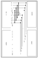
도 1은 종래기술에 따른 반도체메모리소자의 평면도.1 is a plan view of a semiconductor memory device according to the prior art.
도 2는 종래기술에 따른 반도체메모리소자의 입/출력패드로 부터 글로벌 I/O버스까지의 경로를 도시한 도면.2 is a view showing a path from an input / output pad of a semiconductor memory device according to the prior art to a global I / O bus.
도 3은 본 발명의 일 실시예에 따른 반도체메모리소자의 입/출력패드로 부터 글로벌 I/O 버스 까지의 경로를 도시한 도면.3 is a diagram illustrating a path from an input / output pad of a semiconductor memory device to a global I / O bus according to an embodiment of the present invention.
도 4는 본 발명의 일 실시예에 따른 반도체메모리소자의 평면도.4 is a plan view of a semiconductor memory device according to an embodiment of the present invention.
* 도면의 주요 부분에 대한 부호의 설명* Explanation of symbols for the main parts of the drawings
50 : 글로벌 라인50: Global Line
520, 540, 560 : 데이터 경로520, 540, 560: data path
본 발명은 반도체 설계 기술에 관한 것으로, 특히 데이터 폭 옵션에 따른 데 이터 스큐를 줄인 반도체메모리소자에 관한 것이다.BACKGROUND OF THE INVENTION 1. Field of the Invention The present invention relates to semiconductor design technology, and more particularly, to a semiconductor memory device having reduced data skew according to data width options.
통상적으로 데이터 입/출력핀(DQ)을 통해 입력된 데이터를 메모리 셀 어레이로 전달하기 위한 데이터 버스를 글로벌 I/O버스(GIO)라 하며, 셀 어레이 내부에는 각 비트라인과 글로벌 I/O버스(GIO) 간의 데이터 전달을 위한 계층적인 I/O버스 구조를 포함하고 있다.In general, a data bus for transferring data input through a data input / output pin (DQ) to a memory cell array is referred to as a global I / O bus (GIO), and each bit line and global I / O bus inside a cell array. It includes a hierarchical I / O bus structure for data transfer between GIOs.
한편, DDR SDRAM과 같은 반도체메모리소자는 16개의 데이터 입/출력핀(DQ)과 16개의 글로벌 I/O 버스(GIO)를 구비하여 ×4, ×8, ×16 데이터 폭 옵션을 지원한다. 따라서, ×16 모드를 선택한 경우에는 각각의 데이터 입/출력핀(DQ)과 그에 대응하는 각각의 글로벌 I/O 버스(GIO)를 통해 데이터를 전송하면 되나, ×4 또는 ×8 모드를 선택한 경우에는 데이터 입/출력핀(DQ)과 글로벌 I/O 버스(GIO)가 1:1로 매칭되지 않기 때문에 데이터 입/출력핀(DQ)을 통해 입력된 데이터를 특정 글로벌 I/O 버스(GIO)로 전달하기 위한 멀티플렉싱 과정이 필요하며, 데이터 멀티플렉서가 이러한 역할을 수행한다.Meanwhile, semiconductor memory devices, such as DDR SDRAM, have 16 data input / output pins (DQ) and 16 global I / O buses (GIO) to support × 4, × 8, and × 16 data width options. Therefore, when the x16 mode is selected, data can be transferred through each data input / output pin (DQ) and the corresponding global I / O bus (GIO), but the x4 or x8 mode is selected. Since the data input / output pins (DQ) and the global I / O bus (GIO) do not match 1: 1, data input through the data input / output pins (DQ) is not assigned to a specific global I / O bus (GIO). A multiplexing process is required to deliver the data, and the data multiplexer plays this role.
또한, DRAM에서, 액티브 커맨드를 인가하고 이어 읽기커맨드 또는 쓰기커맨드를 인가하기 까지 걸리는 시간을 tRCD(RAS to CAS Delay)라고 한다.In DRAM, the time taken to apply an active command and then to a read command or a write command is referred to as tRCD (RAS to CAS Delay).
도 1은 종래기술에 따른 반도체메모리소자의 평면도로서, 데이터 입력패드를 통해 인가된 데이터가 메모리뱅크에 전달되기 까지의 경로를 간략히 나타낸다.FIG. 1 is a plan view of a semiconductor memory device according to the related art, and briefly illustrates a path from which data applied through a data input pad is transferred to a memory bank.
도 1을 참조하면, 반도체메모리소자는 메모리뱅크(BANK0, BANK1, BANK2, BANK3)와, 데이터를 메모리뱅크에 전달하기 위한 글로벌 I/O 버스(UGIO0, UGIO1, …, LGIO2, LGIO3)와, 외부로 부터 데이터를 인가받기 위한 데이터 입/출력패드 (UDQ0, UDQ1, …, LDQ2, LDQ3)와, 데이터 입/출력패드(UDQ0, UDQ1, …, LDQ2, LDQ3)로 부터 글로벌 I/O버스(UGIO0, UGIO1, …, LGIO2, LGIO3)로 데이터를 전달하기 위한 데이터 경로와, 데이터 경로와 데이터 경로 사이에 연결된 글로벌 라인(50)을 구비한다.Referring to FIG. 1, a semiconductor memory device may include a memory bank BANK0, BANK1, BANK2, BANK3, a global I / O bus for transferring data to a memory bank, UGIO0, UGIO1,..., LGIO2, LGIO3, and an external device. Data I / O pads (UDQ0, UDQ1, ..., LDQ2, LDQ3) to receive data from the data I / O bus (UGIO0) from the data I / O pads (UDQ0, UDQ1, ..., LDQ2, LDQ3) , UGIO1,..., LGIO2, LGIO3) and a
참고적으로, DDR 반도체메모리소자인 경우에는 데이터 입/출력패드 마다 2개의 글로벌 라인을 필요로한다. 또한, DDR II 반도체메모리소자의 경우에는 입/출력패드 마다 4개의 글로벌 라인을 필요로 하며, ×8모드에서 동작하는 경우에는 총 32개의 글로벌 라인을 필요로 한다.For reference, in case of a DDR semiconductor memory device, two global lines are required for each data input / output pad. In addition, in the case of the DDR II semiconductor memory device, four global lines are required for each input / output pad, and when operating in the x8 mode, a total of 32 global lines are required.
도 2는 도 1의 반도체메모리소자가 데이터 폭 옵션에 따라 데이터 입/출력패드로 인가된 데이터를 글로벌 I/O버스로 전달하는 경로를 보다 상세히 도시한 도면이다.FIG. 2 is a diagram illustrating in more detail a path through which the semiconductor memory device of FIG. 1 transfers data applied to a data input / output pad to a global I / O bus according to a data width option.
도 2를 참조하면, 종래기술에 따른 반도체메모리소자는 외부로부터 데이터를 인가받기 위한 데이터 입/출력패드(12, 14)와, 데이터스트로브신호(UDQS, LDQS)에 응답하여 인가된 데이터를 정렬하여 출력하기 위한 버퍼부(22, 24)와, 데이터폭옵션신호(×4, ×8)에 응답하여 버퍼부(22,24)의 출력신호를 선택하기 위한 데이터 멀티플렉서(32, 34)와, 구동신호(BAYBD)에 응답하여 데이터 멀티플렉서(32, 34)의 출력신호를 감지 및 증폭하여 버스인가신호(DINSTBp)에 응답하여 글로벌 I/O버스(U_GIO, L_GIO)에 인가하기 위한 입력데이터 감지증폭기(42, 44)를 구비한다.Referring to FIG. 2, the semiconductor memory device according to the related art arranges the data input /
한편, 전술한 바와같이 반도체메모리소자는 데이터 폭 옵션에 따라 액티브되는 데이터 입/출력패드가 달라진다.Meanwhile, as described above, the data input / output pads that are activated vary according to the data width option.
구체적으로 살펴보면, ×16모드에서는 모든 데이터 입/출력패드가 활성화되므로, UDQ/UDM 패드(12) 및 LDQ/LDM 패드(14)로 인가되는 데이터는 각각의 경로를 통해 해당 글로벌 I/O 버스 UGIO 및 LGIO로 인가되는 반면, ×4 또는 ×8 모드에서는 LDQ/LDM패드(14)만이 액티브되므로, 이를 통해 인가된 데이터는 어드레스에 따라 글로벌 I/O버스 UGIO 또는 LGIO로 인가된다. 즉, ×4 또는 ×8모드에서 데이터는 LDQ/LDM패드(14)로 입력되지만 실리게되는 글로벌 I/O버스는 어드레스에 따라 UGIO가 될수도 있다.In detail, since all data input / output pads are activated in the x16 mode, data applied to the UDQ /
이와같이, ×8, ×4 모드에서 LDQ/LDM 패드(14)로 입력된 데이터를 UGIO로 전송해야하는 경우, UGIO에 연결된 U_데이터 멀티플렉서(42)가 UDQ/UDM 패드(12) 쪽에 배치되어있기 때문에, L_버퍼부(24)의 출력데이터를 U_데이터 멀티플렉서(32)까지 글로벌 라인(50)을 통해 전달해야 된다.As described above, when data input to the LDQ /
따라서, LDQ/LDM 패드(14)로 인가된 데이터를 LGIO로 전송하는 경우에 비해 UGIO로 전송하는 경우 더 오랜 시간이 걸리는데, 이는 LDQ/LDM패드(14)로 인가된 데이터가 UGIO로 전송되기 위해서는 글로벌라인(50)을 거쳐야되므로, 글로벌 라인에 의한 지연만큼 스큐(skew)가 발생하는 것이다.Therefore, it takes longer to transmit data to the UGIO than to the data transmitted to the LDQ /
한편, DRAM은 내부적으로 클럭 신호에 동기되어 동작하도록 되어있기 때문에, LDQ/LDM 패드(14)로 인가된 데이터가 UGIO로 전송되는 경우나 LGIO로 전송되는 경우, 모두 하나의 클럭신호에 동기되어 동작해야 한다.On the other hand, since the DRAM operates internally in synchronization with the clock signal, when the data applied to the LDQ /
그런데, 전술한 바와같이 LDQ/LDM패드(14)로 인가된 데이터가 UGIO로 전송되는 경우와, LGIO로 전송되는 경우 사이에 스큐가 발생하게 되면, 하나의 클럭신호 에 동기하여 동작하도록 타이밍을 조절하는 것이 힘들어진다. 즉, 타이밍 조절에 있어서의 마진이 스큐만큼 줄어드는 것이다.However, as described above, when skew occurs between the data applied to the LDQ /
또한, 요즘과 같이 메모리의 동작이 고속화됨에 따라 클럭의 주기가 짧아지는 경우에는 타이밍 마진을 확보하는 것이 더욱 어렵다.In addition, it is more difficult to secure a timing margin when the clock cycle becomes shorter as the operation of the memory becomes faster as in the past.
그러므로, 종래기술에 따른 반도체메모리소자를 사용하는 경우, 데이터 스큐가 발생하여, 스펙에 따른 클럭 주파수를 얻을 수 없어 칩이 페일되는 문제점이 발생한다.Therefore, in the case of using the semiconductor memory device according to the prior art, data skew occurs, so that the clock frequency according to the specification cannot be obtained, thereby causing a chip failure.
본 발명은 상기와 같은 종래 기술의 문제점을 해결하기 위하여 제안된 것으로, 데이터 폭 옵션에 따라 데이터 입/출력핀을 통해 인가된 데이터가 글로벌 I/O버스에 도달하기 까지 걸리는 지연시간이 달라지는 스큐문제를 해결하기 위한 반도체메모리소자를 제공하는데 그 목적이 있다.
The present invention has been proposed to solve the above problems of the prior art, and the skew problem of varying the delay time until the data applied through the data input / output pin reaches the global I / O bus depends on the data width option. It is an object of the present invention to provide a semiconductor memory device for solving the problem.
상기의 기술적 과제를 달성하기 위한 본 발명의 일 측면에 따른 반도체메모리소자는 칩의 일측방에 형성된 제1 데이터입출력패드; 칩의 타측방에 형성된 제2 데이터입출력패드; 상기 제1 데이터입출력패드로 부터 데이터를 전달받는 제1 글로벌데이터버스; 상기 제2 데이터입출력패드로 부터 데이터를 전달받는 제2 글로벌데이터버스; 상기 제1 데이터입출력패드로 부터 상기 제1 글로벌데이터버스로 데이터 를 전달하는 제1 데이터경로; 상기 제2 데이터입출력패드로 부터 상기 제2 글로벌데이터버스로 데이터를 전달하는 제2 데이터경로; 및 데이터 폭 옵션에 따라 상기 제2 데이터입출력패드에 입력된 데이터를 상기 제1 글로벌데이터버스에 전달하기 위한 제3 데이터경로를 포함하며, 상기 제2 데이터경로와 상기 제3 데이터경로는 실질적으로 동일한 데이터전달 시간을 갖도록 구성된 것을 특징으로 한다.According to one aspect of the present invention, a semiconductor memory device includes: a first data input / output pad formed on one side of a chip; A second data input / output pad formed on the other side of the chip; A first global data bus receiving data from the first data input / output pad; A second global data bus receiving data from the second data input / output pad; A first data path transferring data from the first data input / output pad to the first global data bus; A second data path transferring data from the second data input / output pad to the second global data bus; And a third data path for transferring data input to the second data input / output pad to the first global data bus according to a data width option, wherein the second data path and the third data path are substantially the same. Characterized in that configured to have a data transfer time.
이하, 본 발명이 속하는 기술분야에서 통상의 지식을 가진 자가 본 발명의 기술적 사상을 용이하게 실시할 수 있을 정도로 상세히 설명하기 위하여, 본 발명의 가장 바람직한 실시예를 첨부된 도면을 참조하여 설명하기로 한다.DETAILED DESCRIPTION Hereinafter, exemplary embodiments of the present invention will be described with reference to the accompanying drawings so that those skilled in the art may easily implement the technical idea of the present invention. do.
도 3은 본 발명의 일 실시예에 따른 반도체메모리소자의 평면도로서, 살펴보면 메모리뱅크(BANK0, BANK1, BANK2, BANK3)와, 칩의 일측방 및 타측방에 형성되어 외부로 부터 데이터를 인가받는 데이터 입/출력패드(UDQ0 ∼ UDQ3, …, LDQ0 ∼ LDQ3, …)와, 데이터를 메모리뱅크(BANK0, BANK1, BANK2, BANK3)에 전달하기 위한 글로벌 I/O 버스(UGI0 ∼ UGI3, …, LGI0 ∼ LGI03, …)와, 각각의 데이터 입/출력패드(UDQ0 ∼ UDQ3, …, LDQ0 ∼ LDQ3, …)에 인가된 데이터를 글로벌 I/O 버스(UGI0 ∼ UGI3, …, LGI0 ∼ LGI03, …)에 전달하기 위한 데이터경로(520, 560)와, 데이터폭옵션에 따라 데이터 입/출력패드 LDQ0 ∼ LDQ3, …에 인가된 데이터를 글로벌 I/O 버스 UGI0 ∼ UGIO3, …에 전달하기 위한 데이터 경로 540를 구비한다.FIG. 3 is a plan view of a semiconductor memory device according to an embodiment of the present invention. Referring to FIG. 3, the memory banks BANK0, BANK1, BANK2, and BANK3 are formed on one side and the other side of the chip to receive data from the outside. Input / output pads (UDQ0 to UDQ3, ..., LDQ0 to LDQ3, ...) and global I / O buses (UGI0 to UGI3, ..., LGI0 to LGI03, ..., and data applied to each of the data input / output pads UDQ0-UDQ3, ..., LDQ0-LDQ3, ... are transferred to the global I / O buses UGI0-UGI3, ..., LGI0-LGI03, ...). Data input / output pads LDQ0 to LDQ3,... According to the
이와같이 전술한 본 발명에 따른 반도체메모리소자는 데이터 입/출력패드 LDQ0 ∼ LDQ3, …로 인가된 데이터를 글로벌 I/O 버스 UGI0 ∼ UGIO3, …로 전송하기 위한 데이터 경로 540를 별도로 구비하므로서, 데이터 입/출력패드 LDQ0 ∼ LDQ3, …로 인가된 데이터를 글로벌 I/O 버스 UGI0 ∼ UGIO3, … 또는 LGI0 ∼ LGI03, …로 전송하는데 따른 지연시간이 동일하여져 종래와 같은 스큐문제가 발생하지 않는다. 따라서, 데이터 스트로브신호와 내부클럭 사이의 시간차이를 의미하는 tDQSS를 정교하게 조절할 수 있어 스펙에 따른 클럭 주파수를 얻을 수 있다. 칩의 수율이 향상된다.As described above, the semiconductor memory device according to the present invention includes the data input / output pads LDQ0 to LDQ3,... The data applied to the global I / O buses UGI0 to UGIO3,... The data input / output pads LDQ0 to LDQ3,... The data applied to the global I / O buses UGI0 to UGIO3,... Or LGI0 to LGI03,... The delay time for transmitting the data is the same, so that the skew problem does not occur as in the prior art. Therefore, tDQSS, which represents a time difference between the data strobe signal and the internal clock, can be finely adjusted to obtain a clock frequency according to the specification. The yield of the chip is improved.
또한, 전술한 본 발명에 따른 반도체메모리소자는 데이터 입/출력패드 LDQ0 ∼ LDQ3, …로 인가된 데이터를 글로벌 I/O 버스 UGI0 ∼ UGIO3, …로 전송하기 위한 종래의 글로벌라인을 필요로 하지 않는다. 즉, DDR 반도체메모리소자는 각 데이터입/출력패드 당 2개의 글로벌 라인을 줄일 수 있다. DDR II 반도체메모리소자는 각 데이터 입/출력 패드 당 4개의 글로벌 라인을 줄일 수 있으며, ×8 모드인 경우에는 총 32개의 글로벌 라인을 줄일 수 있다.In addition, the semiconductor memory device according to the present invention described above includes data input / output pads LDQ0 to LDQ3,. The data applied to the global I / O buses UGI0 to UGIO3,... There is no need for a conventional global line to transmit to. That is, the DDR semiconductor memory device can reduce two global lines for each data input / output pad. DDR II semiconductor memory devices can reduce four global lines per data input / output pad, and in total, 32 global lines can be reduced in the x8 mode.
도 4는 도 3의 반도체메모리소자가 데이터 폭 옵션에 따라 데이터 입/출력패드로 인가된 데이터를 글로벌 I/O버스로 전달하는 경로를 보다 상세히 도시한 도면이다.FIG. 4 is a diagram illustrating a path in which the semiconductor memory device of FIG. 3 transfers data applied to a data input / output pad to a global I / O bus according to a data width option.
도 4를 참조하여 각 데이터 입/출력패드(120, 140)에 인가된 데이터를 글로벌 I/O버스에 전달하기 위한 데이터 경로(520, 540, 560, 도 3참조)를 살펴보면, 각 데이터 경로는 데이터스트로브신호(UDQS, LDQS)에 응답하여 데이터 입/출력패드(120, 140)로 인가된 데이터를 정렬하여 출력하기 위한 버퍼부(220, 240)와, 데이터 폭 옵션(×4, ×8)에 따라 버퍼부(220, 240)의 출력신호를 선택하여 전달하기 위한 데이터 멀티플렉서(320, 340, 360)와, 구동신호(BAYBD)에 응답하여 데이터 멀 티플렉서(320, 340, 360)의 출력신호를 감지 및 증폭하고, 버스인가신호(DINSTBp)에 응답하여 증폭된 신호를 글로벌 I/O 버스(UGIO, LGIO)에 전달하기 위한 입력데이터 감지증폭기(420, 440, 460)를 포함한다.Referring to FIG. 4, a
그리고 LDQ/LDM 패드(140)로 인가된 데이터를 글로벌 I/O 버스 LGIO 및 UGIO로 전달하기 위한 각각의 데이터 경로는 L_버퍼부(240)를 공유한다.Each data path for transferring data applied to the LDQ /
다음에서는 전술한 반도체메모리소자가 ×4 또는 ×8모드에서 LDQ/LDM 패드(140)에 입력된 데이터를 글로벌 I/O 버스 UGIO로 전송하는 과정을 간략히 살펴보도록 한다.Next, the process of transferring the data input to the LDQ /
먼저, LDQ/LDM 패드(140)에 입력된 데이터는 L_버퍼부(240)를 거쳐 정렬되며, 데이터 폭 옵션(×4, ×8)에 의해 U_데이터 멀티플렉서(340)가 선택되어 U_입력데이터 감지증폭기(440)로 전달된다. 또한, 구동신호(BAYBD)에 의해 액티브된 U_입력데이터 감지증폭기(440)가 데이터를 감지 및 증폭한 뒤 버스인가신호(DINSTBp)에 응답하여 글로벌 I/O버스 UGIO에 데이터를 인가한다.First, the data input to the LDQ /
참고적으로, ×16 모드의 경우 UDQ/UDM 패드(120)로 인가된 데이터는 경로에 따른 U_버퍼부(220), U_데이터 멀티플렉서(320), U_데이터 감지증폭기(420)를 거쳐 글로벌 I/O 버스 UGIO에 전달되며, LDQ/LDM 패드(140)로 인가된 데이터 역시도 자신의 경로에 따라 글로벌 I/O버스 LGIO로 전달된다.For reference, in the case of the x16 mode, data applied to the UDQ /
그러므로, 전술한 본 발명에 따른 반도체메모리소자는 데이터 입/출력패드로 인가된 데이터를 해당 글로벌 I/O버스에 전송하기 위한 경로를 가질 뿐만 아니라, 데이터 폭 옵션에 따라 다른 글로벌 I/O버스에 전송하기 위한 경로도 별도로 구비 한다. 즉, 종래와 같이 다른 글로벌 I/O 버스로의 데이터 전송 시 기존 경로를 공유하기 위한 글로벌 라인이 필요치 않으므로, 글로벌 라인으로 인한 스큐를 제거할 수 있다. 이와같이 스큐를 제거할 수 있으므로, 스펙에 따른 클럭의 주파수 확보가 가능하여 칩의 수율을 향상시킨다.Therefore, the semiconductor memory device according to the present invention described above not only has a path for transferring data applied to the data input / output pad to the corresponding global I / O bus, but also to other global I / O buses according to the data width option. The path for transmission is also provided separately. In other words, since a global line for sharing an existing path is not required when transmitting data to another global I / O bus as in the related art, skew due to the global line can be eliminated. Since skew can be eliminated in this way, the frequency of the clock according to the specification can be secured, thereby improving chip yield.
이상에서 설명한 본 발명은 전술한 실시예 및 첨부된 도면에 의해 한정되는 것이 아니고, 본 발명의 기술적 사상을 벗어나지 않는 범위 내에서 여러 가지 치환, 변형 및 변경이 가능하다는 것이 본 발명이 속한 기술분야에서 통상의 지식을 가진 자에게 있어 명백할 것이다.The present invention described above is not limited to the above-described embodiments and the accompanying drawings, and various substitutions, modifications, and changes are possible in the art without departing from the technical spirit of the present invention. It will be clear to those of ordinary knowledge.
전술한 본 발명에 따른 반도체메모리소자는 데이터 입/출력패드로 인가된 데이터를 해당 글로벌 I/O버스에 전송하기 위한 경로를 가질 뿐만 아니라, 데이터 폭 옵션에 따라 다른 글로벌 I/O버스에 전송하기 위한 경로도 별도로 구비하므로, 데이터간의 스큐를 제거할 수 있어 스펙에서 요구하는 클럭 주파수를 확보할 수 있다.
The semiconductor memory device according to the present invention described above not only has a path for transferring data applied to a data input / output pad to a corresponding global I / O bus, but also transfers to another global I / O bus according to a data width option. A separate path is also provided, so that skew between data can be eliminated, thereby securing a clock frequency required by the specification.
Claims (5)
Priority Applications (2)
| Application Number | Priority Date | Filing Date | Title |
|---|---|---|---|
| KR1020040070848A KR100550643B1 (en) | 2004-09-06 | 2004-09-06 | Semiconductor memory device |
| US11/024,907 US7616630B2 (en) | 2004-09-06 | 2004-12-30 | Semiconductor memory device |
Applications Claiming Priority (1)
| Application Number | Priority Date | Filing Date | Title |
|---|---|---|---|
| KR1020040070848A KR100550643B1 (en) | 2004-09-06 | 2004-09-06 | Semiconductor memory device |
Publications (1)
| Publication Number | Publication Date |
|---|---|
| KR100550643B1 true KR100550643B1 (en) | 2006-02-09 |
Family
ID=35460391
Family Applications (1)
| Application Number | Title | Priority Date | Filing Date |
|---|---|---|---|
| KR1020040070848A Expired - Fee Related KR100550643B1 (en) | 2004-09-06 | 2004-09-06 | Semiconductor memory device |
Country Status (2)
| Country | Link |
|---|---|
| US (1) | US7616630B2 (en) |
| KR (1) | KR100550643B1 (en) |
Cited By (1)
| Publication number | Priority date | Publication date | Assignee | Title |
|---|---|---|---|---|
| US7940576B2 (en) | 2008-04-30 | 2011-05-10 | Hynix Semiconductor Inc. | Semiconductor device |
Families Citing this family (7)
| Publication number | Priority date | Publication date | Assignee | Title |
|---|---|---|---|---|
| US7227805B2 (en) * | 2004-05-10 | 2007-06-05 | Hynix Semiconductor Inc. | Semiconductor memory device having a global data bus |
| KR100735527B1 (en) * | 2006-02-13 | 2007-07-04 | 삼성전자주식회사 | Semiconductor memory device including two pad rows |
| WO2008063199A1 (en) * | 2006-11-20 | 2008-05-29 | Rambus Inc. | Memory systems and methods for dynamically phase adjusting a write strobe and data to account for receive-clock drift |
| KR101917295B1 (en) * | 2011-10-27 | 2018-11-14 | 에스케이하이닉스 주식회사 | Semiconductor memory device |
| US9779813B2 (en) | 2015-09-11 | 2017-10-03 | Macronix International Co., Ltd. | Phase change memory array architecture achieving high write/read speed |
| KR102643710B1 (en) * | 2016-09-20 | 2024-03-06 | 에스케이하이닉스 주식회사 | Resistance variable memory apparatus |
| US11061431B2 (en) * | 2018-06-28 | 2021-07-13 | Micron Technology, Inc. | Data strobe multiplexer |
Citations (3)
| Publication number | Priority date | Publication date | Assignee | Title |
|---|---|---|---|---|
| KR20000042413A (en) * | 1998-12-24 | 2000-07-15 | 김영환 | Device for selectively driving global input/output line in semiconductor memory device |
| KR20020058586A (en) * | 2000-12-30 | 2002-07-12 | 박종섭 | Method for Transition X16 to X4 and X8 of Same Memory |
| KR20030028473A (en) * | 2001-03-21 | 2003-04-08 | 마이크론 테크놀로지, 인크 | Memory device and method having data path with multiple prefetch I/O configurations |
Family Cites Families (15)
| Publication number | Priority date | Publication date | Assignee | Title |
|---|---|---|---|---|
| US5280474A (en) * | 1990-01-05 | 1994-01-18 | Maspar Computer Corporation | Scalable processor to processor and processor-to-I/O interconnection network and method for parallel processing arrays |
| US5604710A (en) * | 1994-05-20 | 1997-02-18 | Mitsubishi Denki Kabushiki Kaisha | Arrangement of power supply and data input/output pads in semiconductor memory device |
| JP3184085B2 (en) * | 1996-03-01 | 2001-07-09 | 株式会社東芝 | Semiconductor storage device |
| JP3825862B2 (en) * | 1997-02-27 | 2006-09-27 | 株式会社ルネサステクノロジ | Synchronous dynamic semiconductor memory device |
| JP4156706B2 (en) * | 1998-05-29 | 2008-09-24 | 株式会社東芝 | Semiconductor memory device |
| JP2000011681A (en) * | 1998-06-22 | 2000-01-14 | Mitsubishi Electric Corp | Synchronous semiconductor memory device |
| US6115300A (en) * | 1998-11-03 | 2000-09-05 | Silicon Access Technology, Inc. | Column redundancy based on column slices |
| JP3557114B2 (en) * | 1998-12-22 | 2004-08-25 | 株式会社東芝 | Semiconductor storage device |
| KR100363079B1 (en) * | 1999-02-01 | 2002-11-30 | 삼성전자 주식회사 | Multi-bank memory device having shared IO sense amplifier by adjacent memory banks |
| JP3668064B2 (en) * | 1999-08-27 | 2005-07-06 | 株式会社東芝 | Semiconductor memory device |
| KR20020002133A (en) | 2000-06-29 | 2002-01-09 | 박종섭 | Column redundancy circuit |
| JP4684394B2 (en) * | 2000-07-05 | 2011-05-18 | エルピーダメモリ株式会社 | Semiconductor integrated circuit device |
| US6803782B2 (en) * | 2002-03-21 | 2004-10-12 | John Conrad Koob | Arrayed processing element redundancy architecture |
| JP4025584B2 (en) | 2002-05-31 | 2007-12-19 | エルピーダメモリ株式会社 | Semiconductor memory device |
| KR100499417B1 (en) | 2003-07-15 | 2005-07-05 | 주식회사 하이닉스반도체 | A method for masking the ringing in SDRAM and the device therefor |
-
2004
- 2004-09-06 KR KR1020040070848A patent/KR100550643B1/en not_active Expired - Fee Related
- 2004-12-30 US US11/024,907 patent/US7616630B2/en active Active
Patent Citations (3)
| Publication number | Priority date | Publication date | Assignee | Title |
|---|---|---|---|---|
| KR20000042413A (en) * | 1998-12-24 | 2000-07-15 | 김영환 | Device for selectively driving global input/output line in semiconductor memory device |
| KR20020058586A (en) * | 2000-12-30 | 2002-07-12 | 박종섭 | Method for Transition X16 to X4 and X8 of Same Memory |
| KR20030028473A (en) * | 2001-03-21 | 2003-04-08 | 마이크론 테크놀로지, 인크 | Memory device and method having data path with multiple prefetch I/O configurations |
Cited By (2)
| Publication number | Priority date | Publication date | Assignee | Title |
|---|---|---|---|---|
| US7940576B2 (en) | 2008-04-30 | 2011-05-10 | Hynix Semiconductor Inc. | Semiconductor device |
| KR101075497B1 (en) * | 2008-04-30 | 2011-10-20 | 주식회사 하이닉스반도체 | Semiconductor memory device |
Also Published As
| Publication number | Publication date |
|---|---|
| US20050276146A1 (en) | 2005-12-15 |
| US7616630B2 (en) | 2009-11-10 |
Similar Documents
| Publication | Publication Date | Title |
|---|---|---|
| US9640233B2 (en) | Semiconductor memory device having inverting circuit and controlling method there of | |
| US7590013B2 (en) | Semiconductor memory devices having variable additive latency | |
| JP4684394B2 (en) | Semiconductor integrated circuit device | |
| US6396766B1 (en) | Semiconductor memory architecture for minimizing input/output data paths | |
| KR100550643B1 (en) | Semiconductor memory device | |
| US10431274B2 (en) | Semiconductor memory device | |
| KR20080087440A (en) | Semiconductor memory device | |
| KR100252050B1 (en) | Synchronous DRAM and data transfer method with multiple memory banks sharing column select lines | |
| KR101097437B1 (en) | Semiconductor memory apparatus and data inout/output method thereof | |
| KR100438779B1 (en) | Synchronous semiconductor memory device comprising multi-bank scheme | |
| JP4704541B2 (en) | Semiconductor integrated circuit device | |
| US7577038B2 (en) | Data input/output multiplexer of semiconductor device | |
| US20220293163A1 (en) | Column selector architecture with edge mat optimization | |
| KR100734323B1 (en) | Semiconductor memory device with distributed data input / output lines | |
| US7209393B2 (en) | Semiconductor memory device and method for multiplexing write data thereof | |
| KR100968443B1 (en) | Semiconductor memory device | |
| US20030156486A1 (en) | Semiconductor memory device capable of reading at high speed | |
| US9396773B2 (en) | Semiconductor device | |
| US20090273365A1 (en) | Data input/output multiplexer of semiconductor device | |
| KR100703834B1 (en) | Memory Chip Architecture for High Speed Operation | |
| US7907466B2 (en) | Semiconductor memory apparatus | |
| KR20140029977A (en) | Semiconductor memory apparatus | |
| KR20140043867A (en) | Semiconductor memory device | |
| US20050102476A1 (en) | Random access memory with optional column address strobe latency of one | |
| KR20080007940A (en) | Split bank structure semiconductor memory device and data input / output method |
Legal Events
| Date | Code | Title | Description |
|---|---|---|---|
| A201 | Request for examination | ||
| PA0109 | Patent application |
St.27 status event code: A-0-1-A10-A12-nap-PA0109 |
|
| PA0201 | Request for examination |
St.27 status event code: A-1-2-D10-D11-exm-PA0201 |
|
| D13-X000 | Search requested |
St.27 status event code: A-1-2-D10-D13-srh-X000 |
|
| D14-X000 | Search report completed |
St.27 status event code: A-1-2-D10-D14-srh-X000 |
|
| E701 | Decision to grant or registration of patent right | ||
| PE0701 | Decision of registration |
St.27 status event code: A-1-2-D10-D22-exm-PE0701 |
|
| GRNT | Written decision to grant | ||
| PR0701 | Registration of establishment |
St.27 status event code: A-2-4-F10-F11-exm-PR0701 |
|
| PR1002 | Payment of registration fee |
St.27 status event code: A-2-2-U10-U11-oth-PR1002 Fee payment year number: 1 |
|
| PG1601 | Publication of registration |
St.27 status event code: A-4-4-Q10-Q13-nap-PG1601 |
|
| PR1001 | Payment of annual fee |
St.27 status event code: A-4-4-U10-U11-oth-PR1001 Fee payment year number: 4 |
|
| PR1001 | Payment of annual fee |
St.27 status event code: A-4-4-U10-U11-oth-PR1001 Fee payment year number: 5 |
|
| PR1001 | Payment of annual fee |
St.27 status event code: A-4-4-U10-U11-oth-PR1001 Fee payment year number: 6 |
|
| PR1001 | Payment of annual fee |
St.27 status event code: A-4-4-U10-U11-oth-PR1001 Fee payment year number: 7 |
|
| PN2301 | Change of applicant |
St.27 status event code: A-5-5-R10-R13-asn-PN2301 St.27 status event code: A-5-5-R10-R11-asn-PN2301 |
|
| PN2301 | Change of applicant |
St.27 status event code: A-5-5-R10-R13-asn-PN2301 St.27 status event code: A-5-5-R10-R11-asn-PN2301 |
|
| FPAY | Annual fee payment |
Payment date: 20130128 Year of fee payment: 8 |
|
| PR1001 | Payment of annual fee |
St.27 status event code: A-4-4-U10-U11-oth-PR1001 Fee payment year number: 8 |
|
| FPAY | Annual fee payment |
Payment date: 20140122 Year of fee payment: 9 |
|
| PR1001 | Payment of annual fee |
St.27 status event code: A-4-4-U10-U11-oth-PR1001 Fee payment year number: 9 |
|
| FPAY | Annual fee payment |
Payment date: 20150121 Year of fee payment: 10 |
|
| PR1001 | Payment of annual fee |
St.27 status event code: A-4-4-U10-U11-oth-PR1001 Fee payment year number: 10 |
|
| PN2301 | Change of applicant |
St.27 status event code: A-5-5-R10-R13-asn-PN2301 St.27 status event code: A-5-5-R10-R11-asn-PN2301 |
|
| FPAY | Annual fee payment |
Payment date: 20160121 Year of fee payment: 11 |
|
| PR1001 | Payment of annual fee |
St.27 status event code: A-4-4-U10-U11-oth-PR1001 Fee payment year number: 11 |
|
| P22-X000 | Classification modified |
St.27 status event code: A-4-4-P10-P22-nap-X000 |
|
| FPAY | Annual fee payment |
Payment date: 20170124 Year of fee payment: 12 |
|
| PR1001 | Payment of annual fee |
St.27 status event code: A-4-4-U10-U11-oth-PR1001 Fee payment year number: 12 |
|
| FPAY | Annual fee payment |
Payment date: 20180122 Year of fee payment: 13 |
|
| PR1001 | Payment of annual fee |
St.27 status event code: A-4-4-U10-U11-oth-PR1001 Fee payment year number: 13 |
|
| P22-X000 | Classification modified |
St.27 status event code: A-4-4-P10-P22-nap-X000 |
|
| PR1001 | Payment of annual fee |
St.27 status event code: A-4-4-U10-U11-oth-PR1001 Fee payment year number: 14 |
|
| PR1001 | Payment of annual fee |
St.27 status event code: A-4-4-U10-U11-oth-PR1001 Fee payment year number: 15 |
|
| PR1001 | Payment of annual fee |
St.27 status event code: A-4-4-U10-U11-oth-PR1001 Fee payment year number: 16 |
|
| PR1001 | Payment of annual fee |
St.27 status event code: A-4-4-U10-U11-oth-PR1001 Fee payment year number: 17 |
|
| PC1903 | Unpaid annual fee |
St.27 status event code: A-4-4-U10-U13-oth-PC1903 Not in force date: 20230203 Payment event data comment text: Termination Category : DEFAULT_OF_REGISTRATION_FEE |
|
| PC1903 | Unpaid annual fee |
St.27 status event code: N-4-6-H10-H13-oth-PC1903 Ip right cessation event data comment text: Termination Category : DEFAULT_OF_REGISTRATION_FEE Not in force date: 20230203 |