JPWO2002078144A1 - Semiconductor device and crystal growth method - Google Patents
Semiconductor device and crystal growth method Download PDFInfo
- Publication number
- JPWO2002078144A1 JPWO2002078144A1 JP2002576070A JP2002576070A JPWO2002078144A1 JP WO2002078144 A1 JPWO2002078144 A1 JP WO2002078144A1 JP 2002576070 A JP2002576070 A JP 2002576070A JP 2002576070 A JP2002576070 A JP 2002576070A JP WO2002078144 A1 JPWO2002078144 A1 JP WO2002078144A1
- Authority
- JP
- Japan
- Prior art keywords
- antimony
- layer
- indium
- nitrogen
- mixed crystal
- Prior art date
- Legal status (The legal status is an assumption and is not a legal conclusion. Google has not performed a legal analysis and makes no representation as to the accuracy of the status listed.)
- Pending
Links
Images


Classifications
-
- H10P14/2901—
-
- B—PERFORMING OPERATIONS; TRANSPORTING
- B82—NANOTECHNOLOGY
- B82Y—SPECIFIC USES OR APPLICATIONS OF NANOSTRUCTURES; MEASUREMENT OR ANALYSIS OF NANOSTRUCTURES; MANUFACTURE OR TREATMENT OF NANOSTRUCTURES
- B82Y20/00—Nanooptics, e.g. quantum optics or photonic crystals
-
- H—ELECTRICITY
- H01—ELECTRIC ELEMENTS
- H01S—DEVICES USING THE PROCESS OF LIGHT AMPLIFICATION BY STIMULATED EMISSION OF RADIATION [LASER] TO AMPLIFY OR GENERATE LIGHT; DEVICES USING STIMULATED EMISSION OF ELECTROMAGNETIC RADIATION IN WAVE RANGES OTHER THAN OPTICAL
- H01S5/00—Semiconductor lasers
- H01S5/20—Structure or shape of the semiconductor body to guide the optical wave ; Confining structures perpendicular to the optical axis, e.g. index or gain guiding, stripe geometry, broad area lasers, gain tailoring, transverse or lateral reflectors, special cladding structures, MQW barrier reflection layers
- H01S5/22—Structure or shape of the semiconductor body to guide the optical wave ; Confining structures perpendicular to the optical axis, e.g. index or gain guiding, stripe geometry, broad area lasers, gain tailoring, transverse or lateral reflectors, special cladding structures, MQW barrier reflection layers having a ridge or stripe structure
- H01S5/223—Buried stripe structure
- H01S5/2231—Buried stripe structure with inner confining structure only between the active layer and the upper electrode
-
- H—ELECTRICITY
- H01—ELECTRIC ELEMENTS
- H01S—DEVICES USING THE PROCESS OF LIGHT AMPLIFICATION BY STIMULATED EMISSION OF RADIATION [LASER] TO AMPLIFY OR GENERATE LIGHT; DEVICES USING STIMULATED EMISSION OF ELECTROMAGNETIC RADIATION IN WAVE RANGES OTHER THAN OPTICAL
- H01S5/00—Semiconductor lasers
- H01S5/30—Structure or shape of the active region; Materials used for the active region
- H01S5/34—Structure or shape of the active region; Materials used for the active region comprising quantum well or superlattice structures, e.g. single quantum well [SQW] lasers, multiple quantum well [MQW] lasers or graded index separate confinement heterostructure [GRINSCH] lasers
- H01S5/343—Structure or shape of the active region; Materials used for the active region comprising quantum well or superlattice structures, e.g. single quantum well [SQW] lasers, multiple quantum well [MQW] lasers or graded index separate confinement heterostructure [GRINSCH] lasers in AIIIBV compounds, e.g. AlGaAs-laser, InP-based laser
-
- H10P14/22—
-
- H10P14/24—
-
- H10P14/2911—
-
- H10P14/3216—
-
- H10P14/3221—
-
- H10P14/3222—
-
- H10P14/3416—
-
- H10P14/3418—
-
- H10P14/3421—
-
- H10P14/3422—
-
- H10P14/3824—
-
- H—ELECTRICITY
- H01—ELECTRIC ELEMENTS
- H01S—DEVICES USING THE PROCESS OF LIGHT AMPLIFICATION BY STIMULATED EMISSION OF RADIATION [LASER] TO AMPLIFY OR GENERATE LIGHT; DEVICES USING STIMULATED EMISSION OF ELECTROMAGNETIC RADIATION IN WAVE RANGES OTHER THAN OPTICAL
- H01S2304/00—Special growth methods for semiconductor lasers
-
- H—ELECTRICITY
- H01—ELECTRIC ELEMENTS
- H01S—DEVICES USING THE PROCESS OF LIGHT AMPLIFICATION BY STIMULATED EMISSION OF RADIATION [LASER] TO AMPLIFY OR GENERATE LIGHT; DEVICES USING STIMULATED EMISSION OF ELECTROMAGNETIC RADIATION IN WAVE RANGES OTHER THAN OPTICAL
- H01S5/00—Semiconductor lasers
- H01S5/10—Construction or shape of the optical resonator, e.g. extended or external cavity, coupled cavities, bent-guide, varying width, thickness or composition of the active region
- H01S5/1003—Waveguide having a modified shape along the axis, e.g. branched, curved, tapered, voids
-
- H—ELECTRICITY
- H01—ELECTRIC ELEMENTS
- H01S—DEVICES USING THE PROCESS OF LIGHT AMPLIFICATION BY STIMULATED EMISSION OF RADIATION [LASER] TO AMPLIFY OR GENERATE LIGHT; DEVICES USING STIMULATED EMISSION OF ELECTROMAGNETIC RADIATION IN WAVE RANGES OTHER THAN OPTICAL
- H01S5/00—Semiconductor lasers
- H01S5/30—Structure or shape of the active region; Materials used for the active region
- H01S5/32—Structure or shape of the active region; Materials used for the active region comprising PN junctions, e.g. hetero- or double- heterostructures
- H01S5/323—Structure or shape of the active region; Materials used for the active region comprising PN junctions, e.g. hetero- or double- heterostructures in AIIIBV compounds, e.g. AlGaAs-laser, InP-based laser
- H01S5/3235—Structure or shape of the active region; Materials used for the active region comprising PN junctions, e.g. hetero- or double- heterostructures in AIIIBV compounds, e.g. AlGaAs-laser, InP-based laser emitting light at a wavelength longer than 1000 nm, e.g. InP-based 1300 nm and 1500 nm lasers
- H01S5/32358—Structure or shape of the active region; Materials used for the active region comprising PN junctions, e.g. hetero- or double- heterostructures in AIIIBV compounds, e.g. AlGaAs-laser, InP-based laser emitting light at a wavelength longer than 1000 nm, e.g. InP-based 1300 nm and 1500 nm lasers containing very small amounts, usually less than 1%, of an additional III or V compound to decrease the bandgap strongly in a non-linear way by the bowing effect
- H01S5/32366—(In)GaAs with small amount of N
-
- H—ELECTRICITY
- H01—ELECTRIC ELEMENTS
- H01S—DEVICES USING THE PROCESS OF LIGHT AMPLIFICATION BY STIMULATED EMISSION OF RADIATION [LASER] TO AMPLIFY OR GENERATE LIGHT; DEVICES USING STIMULATED EMISSION OF ELECTROMAGNETIC RADIATION IN WAVE RANGES OTHER THAN OPTICAL
- H01S5/00—Semiconductor lasers
- H01S5/30—Structure or shape of the active region; Materials used for the active region
- H01S5/34—Structure or shape of the active region; Materials used for the active region comprising quantum well or superlattice structures, e.g. single quantum well [SQW] lasers, multiple quantum well [MQW] lasers or graded index separate confinement heterostructure [GRINSCH] lasers
- H01S5/343—Structure or shape of the active region; Materials used for the active region comprising quantum well or superlattice structures, e.g. single quantum well [SQW] lasers, multiple quantum well [MQW] lasers or graded index separate confinement heterostructure [GRINSCH] lasers in AIIIBV compounds, e.g. AlGaAs-laser, InP-based laser
- H01S5/34306—Structure or shape of the active region; Materials used for the active region comprising quantum well or superlattice structures, e.g. single quantum well [SQW] lasers, multiple quantum well [MQW] lasers or graded index separate confinement heterostructure [GRINSCH] lasers in AIIIBV compounds, e.g. AlGaAs-laser, InP-based laser emitting light at a wavelength longer than 1000nm, e.g. InP based 1300 and 1500nm lasers
-
- H—ELECTRICITY
- H01—ELECTRIC ELEMENTS
- H01S—DEVICES USING THE PROCESS OF LIGHT AMPLIFICATION BY STIMULATED EMISSION OF RADIATION [LASER] TO AMPLIFY OR GENERATE LIGHT; DEVICES USING STIMULATED EMISSION OF ELECTROMAGNETIC RADIATION IN WAVE RANGES OTHER THAN OPTICAL
- H01S5/00—Semiconductor lasers
- H01S5/30—Structure or shape of the active region; Materials used for the active region
- H01S5/34—Structure or shape of the active region; Materials used for the active region comprising quantum well or superlattice structures, e.g. single quantum well [SQW] lasers, multiple quantum well [MQW] lasers or graded index separate confinement heterostructure [GRINSCH] lasers
- H01S5/343—Structure or shape of the active region; Materials used for the active region comprising quantum well or superlattice structures, e.g. single quantum well [SQW] lasers, multiple quantum well [MQW] lasers or graded index separate confinement heterostructure [GRINSCH] lasers in AIIIBV compounds, e.g. AlGaAs-laser, InP-based laser
- H01S5/34346—Structure or shape of the active region; Materials used for the active region comprising quantum well or superlattice structures, e.g. single quantum well [SQW] lasers, multiple quantum well [MQW] lasers or graded index separate confinement heterostructure [GRINSCH] lasers in AIIIBV compounds, e.g. AlGaAs-laser, InP-based laser characterised by the materials of the barrier layers
Landscapes
- Physics & Mathematics (AREA)
- Optics & Photonics (AREA)
- General Physics & Mathematics (AREA)
- Chemical & Material Sciences (AREA)
- Engineering & Computer Science (AREA)
- Nanotechnology (AREA)
- Condensed Matter Physics & Semiconductors (AREA)
- Electromagnetism (AREA)
- Biophysics (AREA)
- Crystallography & Structural Chemistry (AREA)
- Life Sciences & Earth Sciences (AREA)
- Geometry (AREA)
- Semiconductor Lasers (AREA)
Abstract
発光特性を改善するために、半導体レーザ装置(100)は、窒素と、アンチモンと、窒素及びアンチモン以外の一種類以上のV族元素をV族組成として含むIII−V族化合物半導体層(106)を井戸層として備えている。このようなIII−V族化合物半導体層は、インジウムを含む複数の原料を同時に供給する工程と、インジウムを含まずアンチモンを含む複数の原料を同時に供給する工程とを少なくとも含むサイクルを繰り返すことにより形成される。In order to improve emission characteristics, the semiconductor laser device (100) includes a group III-V compound semiconductor layer (106) containing nitrogen, antimony, and at least one group V element other than nitrogen and antimony as a group V composition. As a well layer. Such a group III-V compound semiconductor layer is formed by repeating a cycle including at least a step of simultaneously supplying a plurality of raw materials containing indium and a step of simultaneously supplying a plurality of raw materials containing antimony without containing indium. Is done.
Description
技術分野
本発明は、窒素と、窒素以外の一種類以上のV族元素とを共にV族組成として含むIII−V族化合物半導体結晶を用いた半導体装置、及びその結晶成長方法に関する。
背景技術
近年、III−V族化合物半導体の利用分野を大きく広げる新しい材料系として、V族組成比数%以下の窒素と、砒素,燐とをV族組成として含むIII−V化合物混晶半導体材料が提案された。砒素、燐といったV族元素と窒素とは、原子半径(窒素:0.070nmに対し、砒素:0.118nm、燐:0.110nm)や、電気陰性度(窒素:3.5に対し、砒素:2.4、燐:2.5)が大きく異なることから、窒素と砒素、あるいは窒素と燐、あるいは窒素と砒素と燐とを混晶化することにより特異な物性が生じる。例えばGaInNAsの場合、GaInAsに、それよりも禁制帯幅の大きなGaInNを数%程度混晶化したものと考えられるが、混晶化に伴う禁制帯幅の変化のボーイングが非常に大きく、禁制帯幅の大きな系を数%混晶化しているにもかかわらず混晶化に伴って禁制帯幅が急激に狭くなる現象が見られる。
このようにして得られるGaInNAsは、安価で良質なGaAs基板に概ね格子整合させつつ(あるいは数%以下の歪量で)光ファイバー通信に重要な波長1.3μm、1.55μm、あるいはそれよりも長波長で発光する発光デバイスの発光層に利用することができ、工業的に重要である。
また、このGaInNAsをはじめとする窒素と砒素、あるいは窒素と燐、あるいは窒素と砒素と燐とを混晶化したIII−V族化合物混晶半導体材料を半導体レーザの活性層材料として用いた場合、半導体レーザの温度特性が格段に向上することがJapanese Journal of Applied Physics,Vol.35,part 1,No.2B,Feb.1996,pp.1273−1275(第一従来例)に示されている。すなわち、GaInAsの砒素の一部を窒素に置換した場合、当該混晶半導体材料の禁制帯における伝導帯のエネルギーレベルが低下し、GaAs等の他の材料とのヘテロ接合における伝導帯のエネルギー差ΔEcが大きくなることから、活性層として用いた当該混晶半導体材料への電子の閉じ込めが著しく強くなり、半導体レーザの特性温度T0が著しく大きくなるものである。
Photonics Technology Letters,Vol.10,No.4,April 1998,p.487(第二従来例)には、上記の構成の半導体レーザがより具体的に示されている。すなわち、活性層をGa0.7In0.3N0.01As0.99から成る量子井戸層とGaAsから成るガイド層とで構成し、これをAl0.3Ga0.7Asから成る上下クラッド層で挟んだ半導体レーザ構造をGaAs基板上に作製し、GaAs基板との格子整合系で構築された半導体レーザとしては初めて波長1.31μmにおける室温連続発振が報告されている。
前述の窒素と窒素以外のV族元素(砒素,隣等)とをV族組成に有する混晶系には非常に大きな非混和領域(ミシビリティギャップ)があり、熱平衡状態では安定な混晶系を作らず、窒素を結晶中に混晶化することが困難となっている。この為、混晶中の窒素混晶比を大きくするに連れて発光特性が急激に悪化する問題が生じる。本願発明者の検討によると、窒素の混晶比を増すに連れてフォトルミネッセンスの発光強度が指数関数的に低下することがわかった。
発明の開示
本発明は上記の問題を解決することを目的としたものである。つまり、窒素と窒素以外のV族元素(砒素,燐等)とを混晶化したIII−V族化合物混晶半導体材料の発光特性を著しく改善することが出来る混晶の構成を提供すると共に、優れた特性を有する半導体装置を提供するものである。また、そのような結晶の作製方法を提供する。
本発明の半導体装置は、窒素と、アンチモンと、窒素及びアンチモン以外の一種類以上のV族元素をV族組成として含むIII−V族化合物半導体層を備えたことを特徴とするものである。
このように、アンチモンを、意図的にIII−V族化合物半導体層の組成として取り込んで混晶化させることにより、所定の波長、歪量における各組成の混晶比の組合わせを変化させる点、特に窒素混晶比を低減させた混晶比設計が可能となり、より特性(特に発光特性)に優れたものが得られる。
好適な実施態様においては、上記III−V族化合物半導体層のアンチモンのV族組成比y(0<y<1)が0.02以上である。
混晶比yが0.02以上で1未満のアンチモンの混晶化によるバンドギャップボーイングの効果により、従来よりも少ない窒素組成で所望の禁制帯幅,歪量の該混晶を得ることが出来る。
また、好適な実施態様においては、上記III−V族化合物半導体層に隣接して、他のIII−V族化合物半導体層を備え、上記III−V族化合物半導体層と、該III−V族化合物半導体層との伝導帯のバンド不連続値が250meV以上である。
また、上記他のIII−V族化合物半導体層は、GaAs、またはGaAsと略格子整合するAlGaAs、GaInP、InGaAsPのいずれかのうちから選択したIII−V族化合物半導体であることが好ましい。さらには、上記III−V族化合物半導体層は、波長約1.3μmで発光し、かつアンチモンのV族組成比y(0<y<1)が、
y≦−0.041×ε+0.173 … (1)
ただし、εは歪量(%)
を満たすことが好ましい。
伝導帯のバンド不連続値が250meV以上、あるいはアンチモンの混晶組成が式(1)を満たすことにより、ヘテロ接合を利用した半導体装置(特に発光素子)においては、アンチモンを混晶化しながらも、より特性(特に発光素子における温度特性)の優れたものが得られるようになる。
また、好適な実施態様においては、上記III−V族化合物半導体層は、アルミニウムをそのIII族組成として含む。
さらに、好適な実施態様においては、上記アルミニウムによる禁制帯幅の拡大分を打ち消すために必要なアンチモン組成比以上の量のアンチモンが混晶化されて含まれている。
また、好適な実施態様においては、上記III−V族化合物半導体層における、窒素及びアンチモン以外のV族元素が、砒素である。
また、好適な実施態様においては、上記III−V族化合物半導体層が半導体レーザ素子の活性層、より詳しくは、井戸層をなし、その共振器長が無限大の場合に閾値電流密度が0.3kA/cm2以下である。
本発明の結晶成長方法は、窒素と、アンチモンと、窒素及びアンチモン以外の一種類以上のV族元素をV族組成として含み、かつインジウムをIII族組成として含むIII−V族化合物半導体層の結晶成長方法であり、少なくともインジウムを含む複数の原料を同時に供給する工程Aと、インジウムを含まず、アンチモンを含む複数の原料を同時に供給する工程Bとを有し、該工程Aと該工程Bとを含むサイクルを、一回以上繰り返すことにより結晶成長を行う。
この結晶成長方法は、インジウム原料とアンチモン原料とを時間的に分離(つまり、工程Aと工程Bとに分離)することによって、インジウムを含む混晶に対するアンチモンの混晶化効率の低下と結晶性の悪化を回避できる。
上記サイクルは、上記工程Aと上記工程Bとの間に、インジウムおよびアンチモンを含まない原料を供給して、インジウムおよびアンチモンを含まない層を形成する工程Cを更に含んでいてもよい。
工程Cで形成されるインジウムおよびアンチモンを含まない層の存在により、工程Aで形成されるインジウムを含む層と工程Bで形成されるアンチモンを含む層とが直接接触しないので、工程AとBとを連続して行なう場合には生じ易いこれら両層の界面での非混和性の問題が回避される。
また、上記サイクルは、上記工程A、Bのうちの後の方の工程の後に、インジウムおよびアンチモンを含まない原料を供給して、インジウムおよびアンチモンを含まない層を形成する工程Dを更に含んでいてもよい。
この場合、工程Dで形成されるインジウムおよびアンチモンを含まない層によって、インジウムの表面偏析やアンチモンの熱蒸発を抑制可能である。
なお、上記工程Cおよび工程Dにおいて形成されるインジウムおよびアンチモンを含まない層は、好ましくは、GaAsである。
また、上記工程Cおよび工程Dにおいて形成されるインジウムおよびアンチモンを含まない層の層厚は、好ましくは、1分子層以上、2分子層以下である。このような層厚であれば、下側の層を完全に覆い隠すことができ、しかも、全体の結晶組成に及ぼす影響を最小限に抑えることができる。
窒素原料は、上記工程Aまたは上記工程Bで供給してもよいし、これに代えて、あるいは、これに加えて、上記サイクルが、III族元素源となる原料を含まず、窒素源となる原料を含む構成元素の原料を供給する工程Eをさらに含んでもよい。また、サイクルに含まれる全工程において窒素原料を供給してもよい。
上記サイクルが工程Eを含む場合、上記工程Eの前に、アルミニウム源を含む構成元素の原料を供給する工程Fをさらに含んでいてもよい。これは、特に、窒素原料として、熱分解効率が余り高くないアンモニア等を用いた場合に有効であり、工程Eの前に工程Fを実施することにより、窒素原料の利用効率を高めることができる。
発明を実施するための最良の形態
(実施の形態1)
図1に、本願発明の半導体装置の一形態である半導体レーザ素子100を示す。この半導体レーザ素子100はGaAs基板の上に構成され、波長1.3μmでレーザ発振するように設計されている。図1の構成において、活性層である井戸層106を構成する化合物半導体層に最適化された量のSbが混晶化されている点に特徴がある。各部の詳細は次の通りである。
半導体レーザ素子100は、波長1.3μmでレーザ発振した。共振器長(L)を300μmとした時のレーザ発振開始時の閾値電流密度Jthは0.4kA/cm2であり、低電流でのレーザ発振が見られた。素子温度20℃から90℃における特性温度T0は187Kであり、温度特性に優れていた。
図2に、この半導体レーザ素子の閾値電流密度Jthと共振器長Lの関係について示す。比較のため、後述する比較例1の半導体レーザ素子の場合についても示している。図2中、E1は実施形態1を、C1は比較例1を表す。図2から明らかなように、実施形態1の半導体レーザ素子のL→∞での閾値電流密度Jth(つまり1/L→0に外挿した時の値)は0.19kA/cm2であった。
(実施の形態2,3)
実施形態1で詳細を説明した半導体レーザ構造の井戸層106を、
実施形態2では、i−Ga0.67In0.33N0.0052As0.9748Sb0.02,7nm,歪量2.4%に、
実施形態3では、i−Ga0.735In0.265N0.0032As0.9218Sb0.075,7nm,歪量2.4%に、
置換した構造の半導体レーザを作製した。作製方法等の詳細は実施形態1と同じであるが、井戸層の各元素の組成が異なる。
上記の半導体レーザ素子についても、作製方法、リッジの幅は、実施形態1と同じである。
何れの半導体レーザ素子についても、波長1.3μmでレーザ発振した。共振器長L→∞での閾値電流密度Jthは、実施形態2において0.3kA/cm2、実施形態3において0.22kA/cm2であり、低電流でのレーザ発振が見られた。素子温度20℃から90℃における特性温度T0は、実施形態2,3において、それぞれ182K,180Kであり、温度特性に優れていた。
(比較例1)
実施形態1で詳細を説明した半導体レーザ構造の井戸層106を、
i−Ga0.65In0.35N0.006As0.994,7nm,歪量2.4%
に置換した構造の半導体レーザを作製した。作製方法等の詳細は実施形態1と同じであるが、井戸層に、従来例と同様にアンチモンが混晶化されていない点が異なる。
上記の半導体レーザ素子についても、作製方法、リッジの幅は、実施形態1と同じである。
この半導体レーザ素子についても、波長1.3μmでレーザ発振した。素子温度20℃から90℃における特性温度T0は183Kであった。
図2に、この半導体レーザ素子の閾値電流密度Jthと共振器長Lの関係について示す。共振器長Lを1/L→0に外挿した時の閾値電流密度Jthは、2.0kA/cm2であった。
(比較例2)
実施形態1で詳細を説明した半導体レーザ構造の井戸層106を、
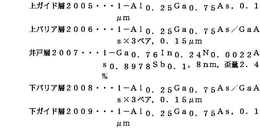
i−Ga0.76In0.24N0.0022As0.8978Sb0.1,7nm,歪量2.4%
に置換した構造の半導体レーザを作製した。作製方法等の詳細は実施形態1と同じであるが、井戸層の各元素の組成が異なる。
上記の半導体レーザ素子についても、作製方法、リッジの幅は、実施形態1と同じである。
この半導体レーザ素子についても、波長1.3μmでレーザ発振した。共振器長L→∞での閾値電流密度Jthは、0.19kA/cm2であった。素子温度20℃から90℃における特性温度T0は120Kであった。
以下に、実施形態1〜3、比較例1,2を参照しながら、本発明の作用と効果について述べる。
比較例1では、GaAsに35%のインジウムと0.6%の窒素とを混晶化することによって当該層の禁制帯幅を狭くし、波長1.3μmで発光する禁制帯幅である0.96eVに調節している。GaAsにインジウムを混晶化した場合、禁制帯幅はGaAsよりも狭くなり、また、格子定数が大きくなる。一方、窒素を混晶化した場合には、禁制帯幅は同じくGaAsよりも狭くなり、また、格子定数は逆に小さくなる。GaAsにインジウムと窒素とを共に混晶化することによって禁制帯幅を狭くし、所定の波長で発光し、所定の歪量を有するように混晶比の組み合わせを決定する。この時、インジウムの混晶比を大きくし過ぎると、格子定数がGaAsから大きく離れるために格子が歪み、結晶欠陥が入りやすくなる。インジウム混晶比の上限はこの歪量の設定値から制限される。
一方、窒素の混晶比は大きくするに連れ、前述の様に、発光特性が急激に悪化する問題がある。窒素混晶比の上限は、この点から制限される。上記の混晶比の制限を念頭におき、混晶材料GaInNAsの禁制帯幅を発光波長1.3μmに調節した結果、比較例1の井戸層が成り立っている。比較例1の場合、井戸層の歪量は2.4%となっている。井戸層の歪量の設定は、通常、他の諸特性との兼ね合いから0〜+3%付近の値に任意に設定される。
一方、実施形態1〜3及び比較例2では、比較例1がGa,In,N,Asの4種類の元素から成っていたのに対し、更に2%以上のSbを混晶化している点に特徴がある。アンチモンは、原子半径がインジウムと同程度で、かつインジウムと同様にGaAsに混晶化すると、禁制帯幅を狭くし、格子定数を大きくする方向に作用する。本願発明者は、従来のGaInNAs混晶において、インジウム混晶比を減らし、その減らした代わりにアンチモンを混晶化することを試みたところ、窒素混晶比を従来よりも少なくしても所望の禁制帯幅の混晶が得られることを見出した。
これは、GaInNAs混晶においてインジウム混晶比を減らす代わりにアンチモンを数〜数十%程度混晶化した場合に、新たに混晶化されたアンチモンに伴うバンドギャップボーイングによる禁制帯幅縮小効果が新たに付加され、窒素混晶比が小さくても所定の狭い禁制帯幅の結晶を得ることが出来るようになるという本願発明者による知見に基づいている。つまり、GaInNAsSb混晶において、アンチモンはインジウムよりもより禁制帯の縮小効率が高くなる現象に基づいている。このことをより具体的に示すために、図3A,3Bには、波長1.3μm,歪量2.4%のGaInNAs混晶にアンチモンを混晶化したGa1− xInxNzAs1−y−zSbyにおけるアンチモン混晶比yとインジウム混晶比x,窒素混晶比zの関係について図示して説明する。この図上の各プロットがそれぞれ実施形態1〜3(図中それぞれE1,E2,E3で表す。)及び比較例1,2(図中、C1,C2で表す。)の構成に対応する。各プロットの構成においては、発光波長、歪量はいずれも1.3μm、2.4%に保たれている。図3A,3Bにおける横軸はアンチモン混晶比yであり、y=0の場合が比較例1に相当する。
ここで、比較例1のGaInNAs混晶にアンチモンを混晶化した場合、図3A,3Bからわかるように、発光波長1.3μm,歪量2.4%の混晶が得られる為のインジウムと窒素の混晶比x,zは、アンチモンの混晶化yと共に減少する方向にシフトする。特にアンチモンを4.5%混晶化した実施形態1の構成においては、アンチモンを混晶化しない場合(比較例1)に対して窒素混晶比を2/3の値に低減することが出来ることがわかった。
図4には、実施形態1〜3(図中それぞれE1,E2,E3で表す。)及び比較例1,2(図中それぞれC1,C2で表す。)の各構成における半導体レーザの、共振器長Lを1/L→0に外挿した時の閾値電流密度Jthをアンチモン混晶比の関数としてプロットしたものである。先に述べたように、窒素混晶比が増加した場合に発光特性が指数関数的に悪化することを考慮すると、アンチモンを混晶化することによって窒素混晶比を2/3にまで減らすことが出来た実施形態1の構成は、著しく発光特性を向上させることにつながり、レーザ素子における発振閾値電流密度の低減、更には発振効率の上昇につながる。特に、アンチモンの混晶比を2%以上とすると、比較例1に対して発振閾値電流密度を大幅に低減することが可能であることが図4からわかり、アンチモンを混晶化することにより初めて発振閾値電流密度0.3kA/cm2以下の優れた半導体レーザを得ることが可能となることがわかった。
更にアンチモン混晶比を増やせば、更に少ない窒素混晶比で波長1.3μmを実現出来、より優れた特性が得られるかのようにも思えるが、アンチモン混晶比の増加・インジウム及び窒素混晶比の減少は、バリア層(図1においては上ガイド層105,下ガイド層107がバリア層として機能している)とのヘテロ接合における伝導帯のエネルギー差ΔEcを小さくすることになり、井戸層への電子の閉じ込めが弱くなるデメリットが生じることがわかった。図5A,5Bに、発光波長1.3μm,歪量2.4%のGa1−xInxNzAs1−y−zSbyとバリア層として用いたGaAsとのヘテロ接合のΔEc,特性温度T0と、アンチモン混晶比yとの相関を示す。
なお、図5Aおよび5Bにおける横軸であるアンチモン混晶比yを変化させた時、インジウム組成xと窒素組成zとは、混晶材料の禁制帯幅及び歪量が一定に保たれるように、図3Aおよび3Bに示した相関に従って変化している。図5Aおよび5Bより、GaInNAs混晶において、アンチモンを混晶化することはΔEcを低下させ、井戸層への電子の閉じ込めを弱くすることになるわけであるが、アンチモン混晶比が7.5%以下であればΔEcは250meV以上が得られ、この場合に180K以上のT0が保たれることがわかる。比較例2のように、アンチモン混晶比を7.5%より大きくすると、T0は急激に小さくなり、好ましくない(比較例2)。このように、バリア層とのバンド不連続の大きさに応じてアンチモンの混晶比を適切な範囲に設定する必要がある。
(実施の形態4,5)
実施形態1で詳細を説明した半導体レーザ構造の井戸層106を、
実施形態4では、i−Ga0.817In0.183N0.0065As0.8985Sb0.095,7nm,歪量1.9%に、
実施形態5では、i−Ga0.95In0.05N0.0122As0.8598Sb0.128,7nm,歪量1.1%に、
置換した構造の半導体レーザを作製した。作製方法等の詳細は実施形態1と同じであるが、井戸層の各元素の組成が異なる。
上記の半導体レーザ素子についても、作製方法、リッジの幅、共振器長は、実施形態1と同じである。
何れの半導体レーザ素子についても、波長1.3μmでレーザ発振した。共振器長Lが300μmの場合におけるレーザ発振開始時の閾値電流密度は、実施形態4,5において、それぞれ0.39kA/cm2,0.42kA/cm2であり、低電流密度でのレーザ発振が見られた。素子温度20℃から90℃における特性温度T0は、実施形態4,5において、それぞれ188K,181Kであり、温度特性に優れていた。
実施形態4,5及び実施形態3における各半導体レーザ素子の井戸層においては、何れも波長1.3μmであり、また、各レーザ素子の井戸層とGaAsバリア層との伝導帯のエネルギー差ΔEcは何れも250meVとなるように井戸層の混晶比が設定、歪量が異なっている。実施形態1〜3において、図5Aを参照しながら説明したように、GaInNAsへアンチモンを混晶化した場合、アンチモン混晶比の増大とともに井戸層とバリア層との伝導帯のエネルギー差ΔEcが低減し、ΔEcを適度な大きさとする為にはアンチモン混晶比に最適な範囲があることを述べた。このアンチモン混晶比の最適な範囲については、バリア層の禁制帯幅・GaInNAsSb混晶の禁制帯幅・インジウム組成・窒素組成等の組み合わせに依存する。
しかしながら、本願発明者は、このアンチモン混晶比の適切な範囲は、バリア層の材料・混晶の禁制帯幅を固定した場合、混晶の歪量の関数として表現することが出来ることを見出した。図6に、バリア層としてGaAsを用いた実施形態3〜5の各構造の歪量ε(%)とアンチモン混晶比yとの関係を図示する。実施形態3〜5(図中、E3〜E5で表す。)では何れも波長1.3μmでありかつΔEc=250meVであることから、図6の各点を結ぶラインがアンチモン混晶比yの上限値の歪量ε依存性ということになる。図6における各点を結ぶラインは、概ね、
y=−0.041×ε+0.173
で近似することが出来る。
このラインで与えられる値以下のアンチモン混晶比y、すなわち
y≦−0.041×ε+0.173 … (1)
で表現される(但し、0<y<1)。図6における斜線領域で混晶を作製すればΔEcが250meV以上となる混晶を作製することが出来、温度特性に優れた半導体レーザが得られることになる。
なお、式(1)は、バリア層がGaAsの場合について導出した式であるが、バリア層がAlGaAs,GaInP,InGaAsPであっても式(1)を満たしていることが望ましい。なぜならば、バリア層がAlGaAsの場合、AlGaAsはGaAsよりも伝導帯のエネルギーレベルが高い為、式(1)を満たしていれば必然的にΔEc≧250meVが確保されるからである。また、GaInP,InGaAsPについては、GaAsと概ね格子整合する組成においては、伝導帯のエネルギーレベルがGaAsと同程度であることから、同様に式(1)を満たしていればΔEc≧250meVが確保されることになる。
(実施の形態6)
図7に、本願発明の半導体装置の一形態である半導体レーザ素子700を示す。この半導体レーザ素子700は、波長1.55μmでレーザ発振するように設計されている点に特徴がある。各部の詳細は次の通りである。
半導体レーザ素子700は、波長1.55μmでレーザ発振した。レーザ発振開始時の閾値電流密度は0.55A/cm2であり、素子温度20℃から90℃における特性温度T0は205Kであった。このように、波長が異なっても2%以上のアンチモンが混晶化されていることにより、アンチモンを混晶化しない場合よりも優れた特性を有する半導体レーザ素子を得ることが出来た。また、アンチモンを混晶化しながらも隣接する層707,709とのヘテロ接合においてはΔEc=300meVの大きな伝導帯バンドギャップ不連続値が確保されており、高い温度特性が得られている。
(実施の形態7)
図8に、本願発明の半導体装置の一形態である半導体レーザ素子800を示す。この半導体レーザ素子800は活性層が多重量子井戸構造であり、各井戸層に、更にアルミニウムが混晶化されている点に特徴がある。各部の詳細は次の通りである。
半導体レーザ素子803は、波長1.3μmでレーザ発振した。レーザ発振開始時の閾値電流密度は0.35A/cm2であり、素子温度20℃から90℃における特性温度T0は195Kであった。このように、GaInNAsSbに更にアルミニウムが混晶化されていても、2%以上のアンチモンが混晶化されていることにより、優れた特性を有する半導体レーザ素子を得ることが出来る。また、アンチモンを混晶化しながらも隣接する層805,807,809とのヘテロ接合においては約300meVの大きな伝導帯バンドギャップ不連続値が確保されており、高い温度特性が得られている。なお、AlGaInNAsSbによって井戸層を構成した半導体レーザ素子は、必ずしも波長1.3μmでレーザ発振するものに限られるわけではなく、1.55μmなどの他の波長であってもよい。
(実施の形態8)
本実施形態においては、原料の間欠供給によってGaInNAsSb混晶を作製する方法について説明する。
ここでは、III族原料,砒素原料,アンチモン原料にはそれぞれの固体金属ソースを用い、窒素原料にはECRプラズマにより活性化されたN2ガスを用い、MBE法により、GaAs(100)基板の上に、基板温度480℃にて結晶成長を行った。図9Aに、結晶成長時の原料の間欠供給の1サイクル分のシーケンスを示す。このシーケンスにおいては、アンチモン供給時(工程12b)にインジウムが供給されていない点にポイントがある。このシーケンスを1サイクル実行するのに4秒を要し、工程12aと工程12bとからなる1サイクルで1分子層相当のGa0.8In0.2N0.01As0.93Sb0.06混晶が結晶成長するように原料ビームの強度を調節した。より具体的には、ガリウム分子線を1.5×10⁻⁷torr、インジウム分子線を3.0×10⁻⁷torr、砒素分子線を前半は1.0×10⁻⁵torr,後半は0.8×10⁻⁵torr、窒素ガス供給量を0.5cc/min、アンチモン分子線を5.0×10−7torrとした。このサイクルを22回繰り返すことにより、62nmの混晶結晶を成長した。
この混晶結晶の、室温におけるPL(フォトルミネッセンス)発光波長は1.3μm、発光の半値全幅は20meVであり、発光強度は非常に強いものであった。
(比較例3)
比較のため、各原料の分子線強度を実施形態8に示した値と同じにしたまま、全ての原料ビームを同時に供給することにより混晶の結晶成長を行った。なお、砒素分子線は0.8×10⁻⁵torrとした。この場合、成長された混晶のアンチモン混晶比は0.01であり、実施形態8の場合の約1/6程度であって、膜中へのアンチモンの取り込みが少なくなることがわかった。また、PL発光強度は実施形態8に対して1/10程度、発光の半値幅は37meVであった。
以下、実施形態8と比較例3とを参照しながら、本発明の作用・効果について説明する。
本願発明者は、GaInNAsSb混晶を成長する際に、インジウム混晶比が高くなるに連れて、膜中へのアンチモンの取り込み効率が著しく低下し、原料効率の点で問題があるとともに、発光特性が悪化することを見出した。これは、インジウムとアンチモンとを両方含む混晶系においては非混和領域が大きく、膜中にインジウムとアンチモンとを同時に取り込むことが難しくなっているためであると思われる。
実施形態8はこの問題を解決するためになされたものである。すなわち、インジウムとアンチモンとの原料供給のタイミングが時間的に分離されているため、アンチモンを供給するタイミングにおいてはインジウムが同時に供給されていないことによって膜中へのアンチモンの取り込み効率が著しく向上しているものである。また、このように非混和性の問題を避けながら結晶成長を行っているため、発光特性においても優れたものが出来るようになるわけである。
なお、図9Aにおいては、インジウム供給時にはアンチモンは一切供給していないが、図9Bに示すようにインジウム供給時(工程13a)にもアンチモンを供給していても問題はない。この時、インジウムと同時に供給されたアンチモンは膜中へ取り込まれにくいが、それに引き続いてインジウムを供給しない状態でアンチモンを供給するシーケンス(工程13b)を設けておけば、それでよい。また、実施形態8においては、インジウムと同時にガリウム,砒素,窒素を、アンチモンと同時にガリウム,砒素を供給しているが、インジウムあるいはアンチモンと同時に供給する他の原料分子線の種類は上記の組み合わせに限定されるものではない。例えば、インジウムと同時にガリウム,砒素を供給し、アンチモンと同時にガリウム,砒素,窒素を供給するシーケンスを設定し、それを繰り返してもよい。また、1サイクルあたりの成長層厚は必ずしも1分子層である必要はなく、2分子層、5分子層、あるいはそれ以上、もしくは自然数でなくとも1.5分子層などの任意の分子層数であってもよい。
なお、実施形態8では基板温度を480℃としたが、基板温度は400℃から500℃の範囲において任意に設定することが出来る。基板温度が400℃よりも低い場合には発光特性の悪化が見られ、基板温度が500℃よりも高い場合には平坦な結晶の成長が困難であった。
(実施の形態9)
図10に、本願発明の半導体装置の一形態である、光通信システムに用いられる光送受信モジュールについて説明する。
図10に、光送受信モジュール1000の略図(斜視図)を示す。基地局から光ファイバー1007を通して送られてきた波長1.3μmの光信号は、a点から光導波路1003に結合され、光導波路1003を導波する。Y分岐部1006では導波されてきた光信号が50:50に分岐され、一方がb点を通して受光用ディテクター部1005に達し、送られてきた光信号が電気信号に変換される。一方送信機能としては、半導体レーザ部1002によって電気信号が光信号に変換され、c点を通して導波路1003に結合され、a点から光ファイバー1007へ送信される。出力モニター部1004は、半導体レーザ1002の光出力を後方からモニターするものである。
この光送受信モジュール1000を構成する送信用半導体レーザ部1002、受光用ディテクター部1005、送信用半導体レーザの出力モニター部1004、光導波路部1003は、GaAs基板1001の上に一回の結晶成長により作製されており、それぞれの微小素子がモノリシック集積されている。送信用半導体レーザ部1002、受光用ディテクター部1005、送信用半導体レーザの出力モニター部1004の層構造は、実施形態1で示したものと同一であり、量子井戸活性層あるいはコア層の井戸層部にGaInNAsSbからなる半導体材料が用いられて高性能化されている。光導波路部1003には、上面から亜鉛が熱拡散され、コア層の量子井戸構造が無秩序化されており、波長1.3μmの光に対して透明となっている。それぞれの微小素子は、ドライエッチングにより加工・分離されている。
この光送受信モジュールでは、送信用半導体レーザ部1002、受光用ディテクター部1005、送信用半導体レーザの出力モニター部1004の井戸層において、砒素と窒素を組成として含むIII−V族化合物半導体材料が用いられているが、更にアンチモンを含むことにより、半導体レーザ部においては低消費電力化、ディテクター・モニター部においては光−電気変換効率が大幅に向上しており、システム全体の性能の向上をはかることができている。
なお、本実施形態においては、層構造として実施形態1で説明したものと同一のものを用いた場合について説明した。一方、これまでに他の実施形態で示してきた種々の組成の組み合わせ、混晶比等を用いて同様のシステムを構築しても同様に高性能なシステムが構築されることは言うまでもない。
上記においては光ファイバー通信システムへの応用について示したが、光ファイバーを用いない空間光伝送システム、あるいは光ディスク用のピックアップ、あるいは光によるセンサー機能を有する光計測システム、レーザを利用した医療用機器などの他の応用システムにおいて同様の構成が可能であり、同様の効果が得られることは言うまでもない。また、必ずしもモノリシック型でなくとも、半導体レーザ部や受光用ディテクター部を外部から貼り付けたハイブリッド型であってもよいことは言うまでもない。
(実施の形態10)
図11に、本願発明の半導体装置の一形態である半導体レーザ素子1100を示す。この半導体レーザ素子1100は活性層が多重量子井戸構造を有するもので、各井戸層にアルミニウムとアンチモンとが混晶化されている点に特徴がある。各部の詳細は次の通りである。
井戸層i−Al0.05Ga0.95−xInxNzAs1−y−zSbyの組成比は、井戸層からの発光波長が1.3μmとなり、かつ井戸層の歪量が2.0%あるいは2.5%となるx,y,zの組み合わせを合計8点選んだ。図12は歪量2.0%、図13は歪量2.5%の場合のx,y,zの組み合わせを、Sb組成比yの関数として図示している。また同時に、得られた井戸層とGaAsから成るバリア層あるいはガイド層との伝導帯のバンド不連続値ΔEcについても図示している。
特定の発光波長(1.3μm)で発光し、一定の歪量(2.0%または2.5%)を有する井戸層i−Al0.05Ga0.95−xInxNzAs1−y−zSbyの組成比に関して、アンチモン混晶比yを増加させるに連れて、インジウム混晶比x及び窒素混晶比zを小さくすることが出来ることが図12,13からわかる。
本願発明者等は、Applied Physics Letters,Vol.78,No.10,2001,p.1364において、窒素と窒素以外のV族元素とを混晶化したIII−V族化合物半導体結晶を結晶成長する際に、アルミニウムを添加しながらMBE法にて結晶成長を行うことによって、アンモニア等の窒素原料の利用効率が著しく増加させることが出来るようになる技術に関して報告している。アルミニウムの混晶化にはこのような利点がある一方で、アルミニウム組成が増すに連れて禁制帯幅が広がってしまう点に問題がある。例えばGaInNAsにアルミニウムを混晶化した場合、アルミニウムによる禁制帯幅の広がりを打ち消す為にはインジウム混晶比や窒素混晶比を増加させる必要があった。特に、窒素混晶比の増加に連れて指数関数的に結晶性(特に発光特性)が悪化するこの混晶系では、窒素の混晶比を増加しなければならないことは重大な問題となり、この混晶系を発光デバイスの発光層に用いた場合には、発光効率の低下、消費電力の増大、素子寿命の短命化につながる。
一方、本願発明においては、アンチモンが混晶化されていることにより、アンチモンの混晶化による効果によって禁制帯幅の縮小が生じており、図12,13に見られるように、一定の禁制帯幅を得るのに必要な窒素混晶比z・インジウム混晶比xを減らすことが出来ている。図12,13において、例えばアンチモン混晶比y=0.08の場合を例に取ると、歪量2.0%とした図12においては窒素混晶比はz=0.01、歪量2.5%とした図13においては窒素混晶比はz=0.006となっている。これは、アルミニウムを混晶化しないGaInNAsで同歪量、同禁制帯幅を実現しようとした場合の窒素混晶比と同等の値となっている。つまり、GaInNAsにアルミニウムとアンチモンとを同時に混晶化した場合、アンチモンは、アルミニウムによる禁制帯幅の拡大分をキャンセルするように作用していることに相当し、アルミニウムを混晶化したことに伴う問題点を解決する方向に作用していることがわかる。GaInNAs等にアルミニウムを含む場合、出来るだけ少ない窒素混晶比で所望の禁制帯幅(=発光波長),歪量を有する優れた結晶を得ようとする場合、アルミニウムとアンチモンとを同時に混晶化することが効果的であると言える。
なお、図12,13の各プロットで示した混晶組成にて作製された半導体レーザ素子1100は、いずれも波長1.3μmでレーザ発振した。レーザ発振開始時の閾値電流は25mAであり、素子温度20℃から90℃における特性温度T0は190Kであった。このように、2%以上のアンチモンが混晶化されていることにより、優れた特性を有する半導体レーザ素子を得ることが出来ている。また、アンチモンを混晶化しながらも隣接する層とのヘテロ接合においては250meV以上の大きな伝導帯バンドギャップ不連続値が確保されており、高い温度特性が得られている。なお、AlGaInNAsSbによって井戸層を構成した半導体レーザ素子は、必ずしも波長1.3μmでレーザ発振するものに限られるわけではなく、1.55μmなどの他の波長であってもよいことは言うまでも無い。
(実施の形態11)
本実施形態においては、原料の間欠供給によってGaInNAsSb混晶を作製する方法について説明する。ここでは、波長1.3μmで発光するGaAs/GaInNAsSb/GaAs単一量子井戸を作製した。
結晶成長は、ガスソース分子線エピタキシャル成長(GS−MBE)法により行った。III族原料,砒素原料,アンチモン原料にはそれぞれの固体金属ソース(金属ガリウム,金属インジウム,金属砒素(As4),金属アンチモン)を用い、窒素原料にはジメチルヒドラジン(DMeHy)を用いた。DMeHyは、ガス状の原料を、クラッキングやプラズマ励起を行わずにガスセルを通して真空チャンバー内に導入し、基板に照射した。基板にはGaAs(100)を用い、結晶成長は基板温度400℃にて行った。
Ga,As4原料を同時に供給することによって層厚1μmのGaAs下バリア層を結晶成長した後、ウエル層であるGaInNAsSbを、図14に示す原料供給シーケンスにて成長を行った。すなわち、まず工程14aにてGa,Sb,Asの原料分子線を9秒間供給した。ここでは、3秒間で、層厚1原子層相当のGaが供給されるように、Gaのビーム強度を2.5×10⁻⁷torrとした。As4,Sbのビーム強度は8.0×10⁻⁶torr,8×10−7torrである。次に工程14bにてIn,Asの原料分子線を9秒間供給した。ここでは、Inのビーム強度を1.6×10⁻⁷torrとした。続いて工程14cにてAs4分子線だけを5秒間照射した。ここではAs4のビーム強度を5.0×10⁻⁶torrにまで低減した。続いて工程14dにて3×10⁻⁶torrのDMeHy分子線とAs4分子線を60秒間照射した。次に、工程14eにて3秒間As4分子線の供給量を行った。ここではAs4のビーム強度を8.0×10⁻⁶torrにまで上昇させた。この工程14aから工程14eよりなる1サイクルを4回繰り返し、層厚約50nmのGaInNAsSb量子井戸を結晶成長した。
作製された井戸層の混晶の各組成の混晶比はGa0.87In0.13N0.01As0.89Sb0.1であった。この混晶結晶の、室温におけるPL(フォトルミネッセンス)発光波長は1.3μm、発光の半値全幅は28meVであり、発光強度は非常に強いものであった。なお、図14における工程14aと工程14bの順序を入れ替えて実施しても同様の結果となった。
以下、実施形態11を参照しながら、本発明の作用・効果について説明する。本願発明者の検討によると、実施形態8で説明したように、アンチモンの混晶化に関して、インジウムを含まない材料系(例えばGaAsやAlGaAs)にアンチモンを混晶化することは容易であるのに対し、インジウムを含む材料系(例えばGaInAs)にアンチモンを混晶化するすることは非常に困難であることがわかった。これは、インジウムを含む混晶系とアンチモンを含む混晶系とを混合した場合の非混和領域が非常に大きくなる為であり、インジウムを含む系とアンチモンを含む系とは安定した混晶相を作らないことによると思われる。
また、アンチモンを効率よく混晶化するには、非平衡度が高い成長条件が望ましく、特に基板温度は400℃から500℃程度の範囲に設定することが望ましいことがわかった。このように基板温度を低くした場合、実施形態8のように窒素原料がプラズマにより活性化されている場合には問題はないが、本実施形態のようにプラズマ活性化されていない分子原料を用いた場合には、原料の熱分解不足により、窒素の添加効率の著しい低下が生じることになる。
本実施形態は、アンチモンの混晶化に有利な低温においても、窒素の添加効率の低下を生じさせない成長シーケンスを示したものである。図14において、工程14aではインジウムを供給しないでアンチモンを供給することによってアンチモンの混晶化を行い、工程14bではインジウムの混晶化を行っている点については実施形態8と同様である。ここでは、その後に工程14dを設けている点に特徴がある。すなわち、III族原料の供給を行わず、窒素原料であるDMeHyを供給しているので、成長層表面に十分な窒素原子を吸着させることが出来るようになっているものである。基板温度400℃という低温ではDMeHyの熱分解は十分ではないが、DMeHyの供給量を適切に設定し、かつ工程14dの時間を適切に設定している為、熱分解の不十分さをDMeHyの供給量と供給時間によって決まる積算供給量によって補償することが出来ている。つまり、III族原料の供給及びアンチモンの混晶化プロセスである工程14a,14bと、窒素の混晶化プロセスである工程14dとを分離することにより、窒素原料の供給条件・供給時間を、III族原料やアンチモンの供給条件・供給時間に左右されることなく設定出来、所望の混晶を得ることが出来るようになったものである。
なお、図14における工程14a,14bは、図15における工程15a,15bのように、入れ替わっていても問題はない。また図9Bを参照しながら説明したように、インジウムを供給する際にもアンチモンを供給していても問題はない。また、III族原料を供給していない工程でもアンチモンを供給していても問題はない。また、ここでは窒素原料は工程14dまたは工程15dだけに供給したが、必ずしもこの工程だけに供給する必要はなく、他の工程で窒素原料を供給してもよく、全ての工程で供給することも可能である。
また、上記の例ではプロセス1サイクル当りの成長層厚を3分子層であるとしたが、必ずしも3分子層である必要はなく、1分子層、5分子層、あるいはそれ以上、もしくは自然数でなくとも1.5分子層などの任意の分子層数であってもよいことは言うまでもない。
窒素原料として、例えばアンモニア(NH3)など、実施形態11で用いたDMeHyよりも熱分解効率が悪いガスを用いた場合、実施形態10で説明したように窒素原料の利用効率を高める為にアルミニウムを添加するのが望ましい。また、アルミニウムによる禁制帯幅の拡大をキャンセルするようにアンチモン混晶比を設定するのが望ましい。このようにアルミニウムを添加しながら窒素の利用を高める時には、図16に示す結晶成長シーケンスを用いることが出来る。すなわち、工程16a,16bでGa,In,As,Sbの混晶化を行った後に工程16cにてAl原料とNH3とを供給し始め、その後に工程16dにてNH3の供給を続けることにより、工程16cにて供給されて結晶表面に付着したアルミニウムの高い反応性を利用しながらNH3からの窒素原子の表面吸着を促進することが出来るようになる。このようなプロセスを用いることにより、アンチモンの混晶化に必要な低温成長と、アルミニウムによる低温での窒素原料の利用効率の向上効果と、アルミニウムとアンチモンの同時混晶化による実施形態10にて示した効果とを全て達成するのに望ましい結晶成長方法となる。
なお、ここでは工程16cにてアルミニウムとNH3とを同時に供給を開始したが、必ずしも同時である必要はなく、NH3は、例えば工程16dだけに供給してもよいし、全工程で供給していてもよい。アルミニウムの供給は、上記の例ではインジウムやガリウムといった他のIII族原料を供給し終わってから再表面に供給したが、インジウムやガリウムと同時であっても問題はない。ただし、その場合には窒素原料の供給を行っている間のアルミニウムの表面露出が少なくなるため、窒素原料の利用効率の向上作用はやや低下する場合がある。
このようにInとSbの原料を時間的に分離して供給し、空間的に分離することによって、非混和性に起因する結晶性の悪化と膜中へのSbの取り込みの低下という問題を回避することが出来るようになったわけであるが、Sb供給前に、InもSbも含まない中間層を挟む図17に示す成長シーケンスを用いた場合、Sbの混晶化を行う為のSb供給工程において下地のInの悪影響を受けなくなり、結晶性の向上とSbの取り込み効率の向上に対して効果的であった。すなわち、In源を含みSb源を含まない原料を供給する工程17aを実施した後、In源もSb源も含まない原料を供給する工程17bを実施し、引き続いてIn源を含まずSb源を含む原料を供給する工程17cを実施する。これにより、工程17aによって形成されるInを含む層と、工程17cによって形成されるSbを含む層の間に、InもSbも含まない中間層(ここではGaAs)が工程17bによって形成されることになり、Inを含む層とSbを含む層とは、その界面も含めて接することがなくなる。よって、Inを含む層とSbを含む層との界面での非混和性の問題が回避されるようになり、結果としてより結晶性に優れた結晶が得られるようになる。なお、工程17aと工程17cとは入れ替わっていてもよい。また、この時の中間層としてはGaAsであることが望ましい。この中間層は、下地を完全に覆い隠す必要があることから1分子層以上である必要があり、また全体の結晶組成に及ぼす影響が少なくなるよう2分子層以下程度であることが望ましい。また、図18に示すように工程18eからのIII族の供給をストップする工程の直前に工程18dに示すようなInもSbも含まないキャップ層を成長することも可能である。このキャップ層により、Inの表面偏析やSbの熱蒸発を抑制することが出来る。このキャップ層もGaAsであることが望ましく、層厚は1分子層以上2分子層以下程度とするのが望ましい。なお、III族元素やSbを供給する各工程は必ずしも連続している必要はなく、例えばAsだけを供給する成長中断時間を設けてもよい。このことは他の全ての実施形態に当てはまる。また各工程でAs供給量は一定とする必要もなく、変化してもよい。例えば図19におけるIn供給工程である工程19aにおけるAs供給量を高めた場合、Inのマイグレーションを抑えて表面の平坦化が促進される効果や、Inの表面偏析を抑制してSbとの空間的分離がより強くなる効果が期待される。
(実施の形態12)
図20に、本願発明の半導体装置の一形態である半導体レーザ素子2000を示す。この半導体レーザ素子2000はGaAs基板を用いて作製され、波長1.3μmでレーザ発振するように設計されている。各部の詳細は次の通りである。
半導体レーザ素子2000は、波長1.3μmでレーザ発振した。共振器長(L)を300μmとした時のレーザ発振開始時の閾値電流密度Jthは0.2kA/cm2であり、低電流でのレーザ発振が見られた。素子温度20℃から90℃における特性温度T0は195Kであり、温度特性に優れていた。
実施形態1〜6においては井戸層であるGaInNAsSbに隣接する層(バリア層またはガイド層)としてGaAsを用いた例を示していたのに対し、本実施形態においてはGaAsよりも禁制帯幅が広いAlGaAsを用いている。その為、GaAsをバリア層として用いた場合よりも、井戸層とバリア層とのヘテロ接合における伝導帯のエネルギー差ΔEcを大きくすることが出来るため、井戸層のアンチモン混晶比をより大きくすることが出来た。それによって井戸層の窒素混晶比をより小さくしても所定の波長の混晶を得ることが出来るようになり、十分な温度特性を保ったまま、より低しきい値電流でのレーザ発振が生じるようになった。上記の構成においては、井戸層であるGaInNAsSbとそれに隣接するAlGaAsとのヘテロ接合における伝導帯のエネルギー差ΔEcとして約300meVの大きな値が確保されている。
なお、図20の構成において下ガイド層から上ガイド層に至る各層の構成は上記に示したものに限られるわけではなく、
また、図20の構成において下ガイド層から上ガイド層に至る各層の構成を、
なお、上記の如く井戸層に隣接するバリア層の禁制帯幅を広げることによって井戸層のアンチモン組成を高くすることが出来るわけであるが、インジウムを含む混晶系とアンチモンを含む混晶系とを混合した場合に生じる非混和領域(ミシビリティギャップ)の影響により、良好な結晶性を保ちつつ混晶化することが出来るアンチモン混晶比にはインジウム混晶比に応じた上限があることがわかった。本願発明者による検討によると、インジウム混晶比が10%,20%,30%の各々の場合に、良好な結晶性を保ちつつ混晶化することが出来るアンチモンの混晶比はそれぞれ30%,20%,10%が上限であった。つまり、インジウム混晶比とアンチモン混晶比の合計が40%以下であることが必要となっている。
なお、本発明は上記の各実施形態に示した特定の結晶系、混晶組成、バンドギャップ波長、ヘテロ接合の組み合わせ、デバイス構造に限定されるものではないことは言うまでもない。特にデバイスについては半導体レーザに限定されるものではなく、発光ダイオード、受光素子、光導波路素子、太陽電池などの任意の光デバイス、あるいはトランジスタ、FET、HEMTなどの電子デバイスの任意の層の作製へ適用することが可能である。
また、本願の実施形態ではIII−V族化合物半導体に数%の窒素を混晶化する場合を取り上げたが、実施形態として詳細を説明した以外のIII族元素(B,Tl等)やV族元素(P,Bi)が適宜混晶化されていてもよいし、不純物元素(C,Zn,Be,Mg,Te,S,Se,Si等)が適宜含まれていてもよい。また、基板についても実施形態に示したものに限定されるものではなく、別の基板を用いても同様の効果が得られる。例えばInGaAs基板などのその他のIII−V族化合物半導体基板、ZnSe基板などのII−VI族化合物半導体基板、Ge,SiC基板などのIV族半導体基板、ガラス・プラスチック・セラミックス等を用いることができる。
これまで示してきた全ての実施形態において、結晶成長方法としては、それぞれの実施形態において示された結晶方法に限定されるものではなく、他の方法を適宜選択し得る。例えば、真空蒸着法、真空スパッタ法、常圧CVD法、MO−MBE法、光CVD法、プラズマCVD法などにも適用することが可能な技術である。
また、結晶成長に用いる各構成元素の原料については、実施形態に記述した特定の原料、あるいはそれぞれの原料の特定の組み合わせに限定されるものではなく、任意の原料を任意の組み合わせで用いることができることは言うまでもない。また、結晶成長により形成された混晶について、各組成の混晶比の組み合わせについても実施形態に記述した特定の値の組み合わせに限定されるものではなく、任意の混晶比の組み合わせとすることが可能である。また、何れも量子井戸構造における井戸層に本願の混晶を適用した場合について示してきたが、その際における井戸数、歪量、井戸層厚に関して制限はない。また、バリア層にも圧縮または引っ張りの歪を導入してもよい。また、量子井戸構造のみならず、バルク結晶であってもよい。
なお、これまでの記述の中で「上」と示された方向は基板から離れる方向を示しており、「下」は基板へ近づく方向を示している。結晶成長は「下」から「上」の方向へ向かって進行する。
以上の説明から明らかなように、本願発明によれば、窒素と、窒素を除くV族元素を含むIII−V族化合物半導体層において、更にアンチモンを混晶化することにより、より特性(特に発光特性)に優れた結晶が得られるようになり、その層を用いた半導体装置において、より特性の優れたものが得られるようになる。特に、発光装置における低い閾値電流密度、高い特性温度を得るのに有効である。
また、本願発明の結晶成長方法では、インジウムとアンチモンとを含む混晶を成長する際のアンチモンの混晶化効率の向上と、結晶性(特に発光特性)の向上を達成することが出来る。
【図面の簡単な説明】
図1は、半導体レーザ装置の斜視図である。
図2は、閾値電流密度と共振器長との相関を示す図である。
図3Aおよび3Bはそれぞれ、GaInNAsSbにおけるアンチモン混晶比yとインジウム混晶比xおよびアンチモン混晶比yと窒素混晶比zとの相関を示す図である。
図4は、閾値電流密度とアンチモン混晶比との相関を示す図である。
図5Aおよび5Bはそれぞれ、ヘテロ接合のΔEcおよび特性温度T0と、アンチモン混晶比xとの相関を示す図である。
図6は、混晶の歪量とアンチモン混晶比の上限との相関を示す図である。
図7は、半導体レーザ装置の斜視図である。
図8は、半導体レーザ装置の斜視図である。
図9Aおよび9Bは、GaInNAsSb成長時の原料供給シーケンスを示す図である。
図10は、光送受信モジュールの斜視図である。
図11は、本発明の半導体装置の一実施形態である半導体レーザ素子の斜視図である。
図12は、発光波長1.3μm、歪量2.0%となるAl0.05Ga0.95−xInxNzAs1−y−zSbyの組成比の組み合わせを、Sb組成比yの関数として図示したものである。また、隣接するGaAs障壁層との伝導帯のバンド不連続値ΔEcについても図示している。
図13は、発光波長1.3μm、歪量2.5%となるAl0.05Ga0.95−xInxNzAs1−y−zSbyの組成比の組み合わせを、Sb組成比yの関数として図示したものである。また、隣接するGaAs障壁層との伝導帯のバンド不連続値ΔEcについても図示している。
図14は、本発明の結晶成長方法の一実施形態である原料の間欠供給によってGaInNAsSb混晶を作製する方法を説明する図であり、各原料を供給するタイミングを示している。
図15は、本発明の結晶成長方法の一実施形態である原料の間欠供給によってGaInNAsSb混晶を作製する方法の変形例を説明する図であり、各原料を供給するタイミングを示している。
図16は、本発明の結晶成長方法の一実施形態である原料の間欠供給によってAlGaInNAsSb混晶を作製する方法の変形例を説明する図であり、各原料を供給するタイミングを示している。
図17は、実施形態11における原料供給シーケンスの変形例を示す図である。
図18は、実施形態11における原料供給シーケンスの変形例を示す図である。
図19は、実施形態11における原料供給シーケンスの変形例を示す図である。
図20は、実施形態12における半導体レーザ装置の斜視図である。Technical field
The present invention relates to a semiconductor device using a group III-V compound semiconductor crystal containing both nitrogen and at least one kind of group V element other than nitrogen as a group V composition, and a crystal growth method thereof.
Background art
In recent years, as a new material system which greatly expands the field of use of III-V compound semiconductors, III-V compound mixed crystal semiconductor materials containing nitrogen having a group V composition ratio of several percent or less, arsenic, and phosphorus as group V compositions have been proposed. Was done. Group V elements such as arsenic and phosphorus and nitrogen have an atomic radius (nitrogen: 0.070 nm, arsenic: 0.118 nm, phosphorus: 0.110 nm) and electronegativity (nitrogen: 3.5, arsenic : 2.4, phosphorus: 2.5), a unique physical property is produced by mixed crystallizing nitrogen and arsenic, or nitrogen and phosphorus, or nitrogen, arsenic and phosphorus. For example, in the case of GaInNAs, it is considered that GaInN mixed with GaInAs having a band gap larger than that of GaInAs by about several% is mixed. However, the change in the band gap caused by the mixed crystal is very large, and the band gap is very large. A phenomenon is seen in which the forbidden band width sharply narrows due to the mixed crystal in spite of the fact that the system having a large width is mixed with several%.
The GaInNAs obtained in this way can have a wavelength of 1.3 μm, 1.55 μm, or longer, which is important for optical fiber communication, while being substantially lattice-matched to a low-cost, high-quality GaAs substrate (or with a strain amount of several percent or less). It can be used for a light emitting layer of a light emitting device that emits light at a wavelength, and is industrially important.
In addition, when using a Ga-InNAs or other III-V compound mixed crystal semiconductor material in which nitrogen and arsenic, or nitrogen and phosphorus, or nitrogen, arsenic and phosphorus are mixed, as an active layer material of a semiconductor laser, The remarkable improvement in the temperature characteristics of a semiconductor laser is described in Japanese Journal of Applied Physics, Vol. 35,
Photonics Technology Letters, Vol. 10, No. 4, April 1998, p. No. 487 (second conventional example) shows the semiconductor laser having the above configuration more specifically. That is, the active layer is made of Ga0.7In0.3N0.01As0.99Composed of a quantum well layer composed of Al and a guide layer composed of GaAs.0.3Ga0.7A semiconductor laser structure in which a semiconductor laser structure sandwiched between upper and lower cladding layers made of As is formed on a GaAs substrate, and continuous oscillation at room temperature at a wavelength of 1.31 μm has been reported for the first time as a semiconductor laser constructed using a lattice matching system with the GaAs substrate.
A mixed crystal system having the above-mentioned nitrogen and a non-nitrogen group V element (arsenic, neighbor, etc.) in a group V composition has a very large immiscible region (miscibility gap) and is stable in a thermal equilibrium state. Therefore, it is difficult to mix nitrogen in the crystal without forming a crystal. For this reason, there arises a problem that the emission characteristics are rapidly deteriorated as the nitrogen mixed crystal ratio in the mixed crystal is increased. According to the study by the present inventors, it has been found that the emission intensity of photoluminescence decreases exponentially as the mixed crystal ratio of nitrogen increases.
Disclosure of the invention
The present invention has been made to solve the above problems. In other words, the present invention provides a mixed crystal structure capable of remarkably improving the light emission characteristics of a III-V compound mixed crystal semiconductor material in which nitrogen and a group V element other than nitrogen (arsenic, phosphorus, etc.) are mixed. An object of the present invention is to provide a semiconductor device having excellent characteristics. Further, a method for producing such a crystal is provided.
The semiconductor device of the present invention is characterized by including a III-V compound semiconductor layer containing nitrogen, antimony, and at least one group V element other than nitrogen and antimony as a group V composition.
As described above, antimony is intentionally taken as the composition of the group III-V compound semiconductor layer and mixed and crystallized, thereby changing the combination of the mixed crystal ratio of each composition at a predetermined wavelength and strain. In particular, it is possible to design a mixed crystal ratio in which the nitrogen mixed crystal ratio is reduced, and to obtain a material having more excellent characteristics (especially, emission characteristics).
In a preferred embodiment, the group V composition ratio y (0 <y <1) of antimony in the group III-V compound semiconductor layer is 0.02 or more.
Due to the effect of bandgap bowing due to the mixed crystal of antimony having a mixed crystal ratio y of 0.02 or more and less than 1, a mixed crystal having a desired bandgap and a desired strain can be obtained with a smaller nitrogen composition than before. .
In a preferred embodiment, another III-V compound semiconductor layer is provided adjacent to the III-V compound semiconductor layer, and the III-V compound semiconductor layer and the III-V compound semiconductor layer are provided. The band discontinuity value of the conduction band with the semiconductor layer is 250 meV or more.
Further, it is preferable that the other group III-V compound semiconductor layer is a group III-V compound semiconductor selected from GaAs or any one of AlGaAs, GaInP, and InGaAsP substantially lattice-matched with GaAs. Further, the III-V group compound semiconductor layer emits light at a wavelength of about 1.3 μm, and the group V composition ratio y (0 <y <1) of antimony is:
y ≦ −0.041 × ε + 0.173 (1)
Where ε is the amount of strain (%)
It is preferable to satisfy the following.
When the band discontinuity value of the conduction band is 250 meV or more, or the mixed crystal composition of antimony satisfies the formula (1), in a semiconductor device using a heterojunction (especially, a light emitting element), while antimony is mixed, More excellent characteristics (in particular, temperature characteristics of the light emitting element) can be obtained.
In a preferred embodiment, the group III-V compound semiconductor layer contains aluminum as its group III composition.
Further, in a preferred embodiment, mixed crystal of antimony is contained in an amount equal to or more than the antimony composition ratio necessary for canceling the increase in the forbidden band width caused by aluminum.
In a preferred embodiment, the group V element other than nitrogen and antimony in the III-V compound semiconductor layer is arsenic.
In a preferred embodiment, the group III-V compound semiconductor layer forms an active layer of a semiconductor laser device, more specifically, a well layer, and has a threshold current density of 0. 3kA / cm2It is as follows.
The crystal growth method of the present invention is directed to a crystal of a III-V compound semiconductor layer containing nitrogen, antimony, and at least one group V element other than nitrogen and antimony as a group V composition, and containing indium as a group III composition. A growth method, comprising a step A of simultaneously supplying a plurality of raw materials containing at least indium, and a step B of simultaneously supplying a plurality of raw materials containing antimony containing no indium, wherein the step A and the step B Is repeated one or more times to perform crystal growth.
This crystal growth method temporally separates an indium raw material and an antimony raw material (that is, separates into a step A and a step B), thereby lowering the efficiency of antimony mixed crystal with respect to the mixed crystal containing indium and reducing the crystallinity. Can be avoided.
The above cycle may further include a step C of forming a layer containing no indium and antimony by supplying a raw material containing no indium and antimony between the above step A and the above step B.
Since the layer containing indium formed in step A and the layer containing antimony formed in step B do not directly contact with each other due to the presence of the layer containing no indium and antimony formed in step C, steps A and B The problem of immiscibility at the interface between these two layers, which tends to occur when the process is performed continuously, is avoided.
Further, the cycle further includes a step D of forming a layer containing no indium and antimony by supplying a raw material containing no indium and antimony after the latter of the above steps A and B. It may be.
In this case, the indium and antimony-free layer formed in step D can suppress surface segregation of indium and thermal evaporation of antimony.
The layer that does not contain indium and antimony and is formed in step C and step D is preferably GaAs.
Further, the layer thickness of the layer not containing indium and antimony formed in the above steps C and D is preferably not less than 1 molecular layer and not more than 2 molecular layers. With such a layer thickness, the lower layer can be completely covered and the influence on the entire crystal composition can be minimized.
The nitrogen source may be supplied in the above step A or the above step B. Alternatively, or in addition to this, the above-mentioned cycle becomes a nitrogen source without containing a raw material serving as a group III element source. The method may further include a step E of supplying a raw material of a constituent element including the raw material. Further, a nitrogen raw material may be supplied in all the steps included in the cycle.
When the cycle includes the step E, the cycle may further include a step F of supplying a raw material of a constituent element including an aluminum source before the step E. This is particularly effective when using ammonia or the like, whose thermal decomposition efficiency is not so high, as the nitrogen source. By performing the step F before the step E, the utilization efficiency of the nitrogen source can be increased. .
BEST MODE FOR CARRYING OUT THE INVENTION
(Embodiment 1)
FIG. 1 shows a
The
FIG. 2 shows the threshold current density J of this semiconductor laser device.thThe relationship between and the resonator length L will be described. For comparison, the case of a semiconductor laser device of Comparative Example 1 described later is also shown. In FIG. 2, E1 represents
(
The
In the second embodiment, i-Ga0.67In0.33N0.0052As0.9748Sb0.02, 7 nm, strain amount 2.4%,
In the third embodiment, i-Ga0.735In0.265N0.0032As0.9218Sb0.075, 7 nm, strain amount 2.4%,
A semiconductor laser having a substituted structure was manufactured. Details of the fabrication method and the like are the same as those of the first embodiment, but the composition of each element of the well layer is different.
The manufacturing method and the ridge width of the above-described semiconductor laser device are the same as those of the first embodiment.
Each of the semiconductor laser devices oscillated at a wavelength of 1.3 μm. Threshold current density J at resonator length L → ∞thIs 0.3 kA / cm in the second embodiment.20.23 kA / cm in the third embodiment2And laser oscillation at a low current was observed. Characteristic temperature T at
(Comparative Example 1)
The
i-Ga0.65In0.35N0.006As0.994, 7 nm, strain 2.4%
Was fabricated. The details of the manufacturing method and the like are the same as those of the first embodiment, except that antimony is not mixed-crystallized in the well layer as in the conventional example.
The manufacturing method and the ridge width of the above-described semiconductor laser device are the same as those of the first embodiment.
This semiconductor laser device also oscillated at a wavelength of 1.3 μm. Characteristic temperature T at
FIG. 2 shows the threshold current density J of this semiconductor laser device.thThe relationship between and the resonator length L will be described. Threshold current density J when the resonator length L is extrapolated from 1 / L to 0thIs 2.0 kA / cm2Met.
(Comparative Example 2)
The
i-Ga0.76In0.24N0.0022As0.8978Sb0.1, 7 nm, strain 2.4%
Was fabricated. Details of the fabrication method and the like are the same as those of the first embodiment, but the composition of each element of the well layer is different.
The manufacturing method and the ridge width of the above-described semiconductor laser device are the same as those of the first embodiment.
This semiconductor laser device also oscillated at a wavelength of 1.3 μm. Threshold current density J at resonator length L → ∞thIs 0.19 kA / cm2Met. Characteristic temperature T at
Hereinafter, the operation and effects of the present invention will be described with reference to
In Comparative Example 1, the forbidden band width of the layer was narrowed by mixing 35% of indium and 0.6% of nitrogen in GaAs, and the band gap of 0.1% which emits light at a wavelength of 1.3 μm. It is adjusted to 96 eV. When indium is mixed with GaAs, the band gap becomes narrower than that of GaAs, and the lattice constant becomes larger. On the other hand, when nitrogen is mixed, the forbidden band width becomes smaller than that of GaAs, and the lattice constant becomes smaller. By mixing indium and nitrogen together in GaAs, the forbidden band width is narrowed, light is emitted at a predetermined wavelength, and a combination of mixed crystal ratios is determined so as to have a predetermined strain amount. At this time, if the mixed crystal ratio of indium is too large, the lattice constant is largely apart from GaAs, so that the lattice is distorted and crystal defects are likely to be formed. The upper limit of the indium mixed crystal ratio is limited by the set value of the strain amount.
On the other hand, as the mixed crystal ratio of nitrogen is increased, there is a problem that the light emission characteristics are rapidly deteriorated as described above. The upper limit of the nitrogen mixed crystal ratio is limited from this point. The well layer of Comparative Example 1 is established as a result of adjusting the forbidden band width of the mixed crystal material GaInNAs to 1.3 μm in light of the above limitation of the mixed crystal ratio. In the case of Comparative Example 1, the strain amount of the well layer was 2.4%. The setting of the strain amount of the well layer is usually set arbitrarily to a value of about 0 to + 3% in consideration of other characteristics.
On the other hand, in the first to third embodiments and the comparative example 2, the comparative example 1 is composed of four kinds of elements of Ga, In, N, and As, whereas 2% or more of Sb is mixed crystal. There is a feature. When antimony has the same atomic radius as indium and is mixed with GaAs in the same manner as indium, it acts to narrow the forbidden band width and increase the lattice constant. The present inventor has attempted to reduce the indium mixed crystal ratio in the conventional GaInNAs mixed crystal and to mix antimony instead of the reduced indium mixed crystal ratio. It has been found that a mixed crystal having a forbidden band width can be obtained.
This is because when the antimony is mixed several to several tens% instead of reducing the indium mixed crystal ratio in the GaInNAs mixed crystal, the bandgap bowing accompanying the newly mixed antimony reduces the forbidden band width. It is based on the inventor's finding that a newly added crystal having a predetermined narrow band gap can be obtained even when the nitrogen mixed crystal ratio is small. That is, in GaInNAsSb mixed crystal, antimony is based on the phenomenon that the forbidden band reduction efficiency is higher than that of indium. To show this more specifically, FIGS. 3A and 3B show a GaInNAs mixed crystal having a wavelength of 1.3 μm and a strain amount of 2.4% mixed with antimony.1- xInxNzAs1-yzSbyThe relationship between the antimony mixed crystal ratio y, the indium mixed crystal ratio x, and the nitrogen mixed crystal ratio z in FIG. The plots on this diagram correspond to the configurations of
Here, when antimony is mixed with the GaInNAs mixed crystal of Comparative Example 1, as can be seen from FIGS. 3A and 3B, indium for obtaining a mixed crystal having an emission wavelength of 1.3 μm and a strain of 2.4% is obtained. The mixed crystal ratio x, z of nitrogen shifts in a decreasing direction with the mixed crystal y of antimony. In particular, in the configuration of
FIG. 4 shows the resonators of the semiconductor lasers in the configurations of
It seems that if the antimony mixed crystal ratio is further increased, a wavelength of 1.3 μm can be realized with a lower nitrogen mixed crystal ratio, and more excellent characteristics can be obtained. The decrease in the crystal ratio reduces the energy difference ΔEc of the conduction band at the heterojunction with the barrier layer (in FIG. 1, the
When the antimony mixed crystal ratio y on the horizontal axis in FIGS. 5A and 5B is changed, the indium composition x and the nitrogen composition z are adjusted so that the forbidden band width and strain amount of the mixed crystal material are kept constant. , According to the correlations shown in FIGS. 3A and 3B. 5A and 5B, in GaInNAs mixed crystal, making antimony into a mixed crystal lowers ΔEc and weakens the confinement of electrons in the well layer, but the antimony mixed crystal ratio is 7.5. % Or less, ΔEc is 250 meV or more, and in this case, T of 180 K or more is obtained.0It can be seen that is maintained. As in Comparative Example 2, when the mixed crystal ratio of antimony is larger than 7.5%, T0Rapidly decreases, which is not preferable (Comparative Example 2). Thus, it is necessary to set the mixed crystal ratio of antimony in an appropriate range according to the size of the band discontinuity with the barrier layer.
(Embodiments 4 and 5)
The
In the fourth embodiment, i-Ga0.817In0.183N0.0065As0.8985Sb0.095, 7nm, strain amount 1.9%,
In the fifth embodiment, i-Ga0.95In0.05N0.0122As0.8598Sb0.128, 7 nm, distortion amount 1.1%,
A semiconductor laser having a substituted structure was manufactured. Details of the fabrication method and the like are the same as those of the first embodiment, but the composition of each element of the well layer is different.
The manufacturing method, ridge width, and resonator length of the above-described semiconductor laser device are the same as those of the first embodiment.
Each of the semiconductor laser devices oscillated at a wavelength of 1.3 μm. The threshold current densities at the start of laser oscillation when the resonator length L is 300 μm are 0.39 kA / cm in Embodiments 4 and 5, respectively.2, 0.42 kA / cm2And laser oscillation at a low current density was observed. Characteristic temperature T at
In each of the well layers of the semiconductor laser devices according to the fourth, fifth, and third embodiments, the wavelength is 1.3 μm, and the energy difference ΔEc of the conduction band between the well layer of each laser device and the GaAs barrier layer is: In each case, the mixed crystal ratio of the well layer is set so as to be 250 meV, and the strain amount is different. As described with reference to FIG. 5A in
However, the present inventor has found that the appropriate range of the antimony mixed crystal ratio can be expressed as a function of the amount of strain of the mixed crystal when the material of the barrier layer and the forbidden band width of the mixed crystal are fixed. Was. FIG. 6 illustrates the relationship between the strain amount ε (%) and the antimony mixed crystal ratio y in each of the structures of
y = −0.041 × ε + 0.173
Can be approximated by
Antimony mixed crystal ratio y equal to or less than the value given by this line, that is,
y ≦ −0.041 × ε + 0.173 (1)
(Where 0 <y <1). If a mixed crystal is produced in the shaded region in FIG. 6, a mixed crystal having ΔEc of 250 meV or more can be produced, and a semiconductor laser having excellent temperature characteristics can be obtained.
The expression (1) is derived from the case where the barrier layer is made of GaAs. However, it is preferable that the expression (1) is satisfied even when the barrier layer is made of AlGaAs, GaInP, or InGaAsP. This is because, when the barrier layer is made of AlGaAs, AlGaAs has a higher conduction band energy level than GaAs, so that if Eq. (1) is satisfied, ΔEc ≧ 250 meV is necessarily secured. For GaInP and InGaAsP, the energy level of the conduction band is almost the same as that of GaAs in a composition that is substantially lattice-matched with GaAs, so that if Eq. (1) is satisfied, ΔEc ≧ 250 meV is similarly secured. Will be.
(Embodiment 6)
FIG. 7 shows a
The
(Embodiment 7)
FIG. 8 shows a
The
(Embodiment 8)
In the present embodiment, a method for producing a GaInNAsSb mixed crystal by intermittent supply of a raw material will be described.
Here, a solid metal source is used for the group III raw material, the arsenic raw material, and the antimony raw material, and N activated by ECR plasma is used for the nitrogen raw material.2Crystal growth was performed at a substrate temperature of 480 ° C. on a GaAs (100) substrate by MBE using a gas. FIG. 9A shows a sequence for one cycle of intermittent supply of the raw material during crystal growth. The point of this sequence is that indium is not supplied when antimony is supplied (
The PL (photoluminescence) emission wavelength of this mixed crystal at room temperature was 1.3 μm, the full width at half maximum of emission was 20 meV, and the emission intensity was very strong.
(Comparative Example 3)
For comparison, a mixed crystal was grown by simultaneously supplying all the material beams while keeping the molecular beam intensity of each material the same as the value shown in the eighth embodiment. The arsenic molecular beam is 0.8 × 10⁻⁵torr. In this case, the antimony mixed crystal ratio of the grown mixed crystal was 0.01, which was about 1/6 of that of the eighth embodiment, and it was found that the incorporation of antimony into the film was reduced. The PL emission intensity was about 1/10 of that of the eighth embodiment, and the half width of the emission was 37 meV.
Hereinafter, the operation and effect of the present invention will be described with reference to Embodiment 8 and Comparative Example 3.
The inventor of the present application has found that when growing a GaInNAsSb mixed crystal, as the indium mixed crystal ratio increases, the efficiency of incorporation of antimony into the film significantly decreases, and there is a problem in terms of raw material efficiency and emission characteristics. Was found to be worse. This is presumably because in a mixed crystal system containing both indium and antimony, the immiscible region is large, making it difficult to incorporate indium and antimony into the film at the same time.
Embodiment 8 has been made to solve this problem. In other words, since the supply timings of indium and antimony are separated in time, at the timing of supplying antimony, the indium is not supplied at the same time, so that the efficiency of incorporation of antimony into the film is significantly improved. Is what it is. In addition, since the crystal growth is performed while avoiding the problem of immiscibility, it is possible to obtain an excellent light emitting characteristic.
Note that in FIG. 9A, no antimony is supplied at the time of supplying indium, but there is no problem even if antimony is supplied at the time of supplying indium (
Although the substrate temperature is set to 480 ° C. in the eighth embodiment, the substrate temperature can be arbitrarily set within a range of 400 ° C. to 500 ° C. When the substrate temperature was lower than 400 ° C., the emission characteristics deteriorated. When the substrate temperature was higher than 500 ° C., it was difficult to grow flat crystals.
(Embodiment 9)
FIG. 10 illustrates an optical transceiver module used in an optical communication system, which is one mode of the semiconductor device of the present invention.
FIG. 10 shows a schematic diagram (perspective view) of the
The transmitting
In this optical transceiver module, a group III-V compound semiconductor material containing arsenic and nitrogen as a composition is used in the well layers of the transmitting
In this embodiment, the case where the same layer structure as that described in the first embodiment is used has been described. On the other hand, needless to say, even if a similar system is constructed using various combinations of compositions, mixed crystal ratios, and the like described in the other embodiments, a similarly high-performance system is constructed.
In the above, the application to the optical fiber communication system has been described. However, a spatial light transmission system without using an optical fiber, a pickup for an optical disk, an optical measurement system having a sensor function by light, a medical device using a laser, and the like. It is needless to say that the same configuration is possible in the application system and the same effect can be obtained. Further, it is needless to say that the type is not necessarily a monolithic type, but may be a hybrid type in which a semiconductor laser unit and a light receiving detector unit are externally attached.
(Embodiment 10)
FIG. 11 shows a
Well layer i-Al0.05Ga0.95-xInxNzAs1-yzSbyA total of eight combinations of x, y, and z were selected so that the emission wavelength from the well layer was 1.3 μm and the strain amount of the well layer was 2.0% or 2.5%. FIG. 12 shows a combination of x, y, and z for a strain amount of 2.0% and FIG. 13 as a function of the Sb composition ratio y for a strain amount of 2.5%. At the same time, the band discontinuity ΔE of the conduction band between the obtained well layer and the barrier layer or the guide layer made of GaAs.cIs also illustrated.
A well layer i-Al that emits light at a specific emission wavelength (1.3 μm) and has a certain amount of strain (2.0% or 2.5%)0.05Ga0.95-xInxNzAs1-yzSbyIt can be seen from FIGS. 12 and 13 that the indium mixed crystal ratio x and the nitrogen mixed crystal ratio z can be reduced as the antimony mixed crystal ratio y is increased.
The inventors of the present application have disclosed Applied Physics Letters, Vol. 78, no. 10, 2001, p. In 1364, when growing a III-V compound semiconductor crystal in which nitrogen and a group V element other than nitrogen are mixed and crystallized, the crystal growth is performed by MBE while adding aluminum, whereby ammonia and the like are grown. It reports on technologies that can significantly increase the utilization efficiency of nitrogen sources. While aluminum alloy has such advantages, it has a problem in that the forbidden band becomes wider as the aluminum composition increases. For example, when GaInNAs is mixed with aluminum, it is necessary to increase the indium mixed crystal ratio and the nitrogen mixed crystal ratio in order to cancel the expansion of the band gap caused by aluminum. In particular, in this mixed crystal system in which the crystallinity (especially the emission characteristics) deteriorates exponentially with an increase in the nitrogen mixed crystal ratio, it is a serious problem that the nitrogen mixed crystal ratio must be increased. When the mixed crystal system is used for the light emitting layer of the light emitting device, the light emitting efficiency is reduced, the power consumption is increased, and the life of the element is shortened.
On the other hand, in the present invention, since the antimony is mixed, the forbidden band width is reduced due to the effect of the antimony mixed crystal, and as shown in FIGS. The nitrogen mixed crystal ratio z and the indium mixed crystal ratio x required to obtain the width can be reduced. 12 and 13, for example, when the antimony mixed crystal ratio y = 0.08, the nitrogen mixed crystal ratio is z = 0.01 and the strain amount is 2 in FIG. In FIG. 13 in which 0.5% is set, the nitrogen mixed crystal ratio is z = 0.006. This is a value equivalent to the nitrogen mixed crystal ratio when trying to realize the same strain and the same forbidden bandwidth with GaInNAs in which aluminum is not mixed crystal. In other words, when aluminum and antimony are simultaneously mixed and crystallized in GaInNAs, antimony is equivalent to acting to cancel the expansion of the forbidden band width due to aluminum, and is caused by the mixed crystal of aluminum. It can be seen that it works in the direction to solve the problem. When GaInNAs or the like contains aluminum, in order to obtain an excellent crystal having a desired forbidden band width (= emission wavelength) and distortion with a nitrogen mixed crystal ratio as small as possible, aluminum and antimony are simultaneously crystallized. Can be said to be effective.
Each of the
(Embodiment 11)
In the present embodiment, a method for producing a GaInNAsSb mixed crystal by intermittent supply of a raw material will be described. Here, a GaAs / GaInNAsSb / GaAs single quantum well emitting at a wavelength of 1.3 μm was fabricated.
The crystal growth was performed by a gas source molecular beam epitaxial growth (GS-MBE) method. Group III raw materials, arsenic raw materials, and antimony raw materials include solid metal sources (metal gallium, metal indium, metal arsenic (As)4), Metal antimony) and dimethylhydrazine (DMeHy) as the nitrogen source. DMeHy introduced a gaseous raw material into a vacuum chamber through a gas cell without performing cracking or plasma excitation, and irradiated the substrate. GaAs (100) was used for the substrate, and crystal growth was performed at a substrate temperature of 400 ° C.
Ga, As4After crystal growth of the GaAs lower barrier layer having a thickness of 1 μm by simultaneously supplying raw materials, GaInNAsSb as a well layer was grown by a raw material supply sequence shown in FIG. That is, first, in
The mixed crystal ratio of each composition of the mixed crystal of the manufactured well layer was Ga.0.87In0.13N0.01As0.89Sb0.1Met. The PL (photoluminescence) emission wavelength at room temperature of this mixed crystal was 1.3 μm, the full width at half maximum of emission was 28 meV, and the emission intensity was very strong. Note that the same result was obtained even when the order of the
Hereinafter, the operation and effect of the present invention will be described with reference to the eleventh embodiment. According to the study by the inventor of the present application, as described in the eighth embodiment, it is easy to mix antimony in a material system containing no indium (for example, GaAs or AlGaAs). On the other hand, it has been found that it is very difficult to mix antimony in a material system containing indium (for example, GaInAs). This is because the immiscible region becomes extremely large when a mixed crystal system containing indium and a mixed crystal system containing antimony are mixed, and a stable mixed crystal phase is obtained between the system containing indium and the system containing antimony. It seems that it is not made.
In addition, it has been found that, in order to efficiently mix antimony, a growth condition having a high non-equilibrium degree is desirable, and it is particularly desirable to set the substrate temperature in a range of about 400 ° C. to 500 ° C. When the substrate temperature is lowered in this manner, there is no problem in the case where the nitrogen source is activated by plasma as in Embodiment 8, but a molecular source that is not plasma-activated as in this embodiment is used. In this case, the efficiency of nitrogen addition is significantly reduced due to insufficient thermal decomposition of the raw material.
The present embodiment shows a growth sequence that does not cause a decrease in nitrogen addition efficiency even at a low temperature that is advantageous for mixed crystal formation of antimony. In FIG. 14, as in Embodiment 8, the mixed crystal of antimony is performed by supplying antimony without supplying indium in
Note that there is no problem even if the
In the above example, the growth layer thickness per one process cycle is three molecular layers. However, the growth layer is not necessarily three molecular layers, and is not one molecular layer, five molecular layers or more, or a natural number. Needless to say, any number of molecular layers such as 1.5 molecular layers may be used.
As a nitrogen source, for example, ammonia (NH3), When a gas having a lower thermal decomposition efficiency than DMeHy used in the eleventh embodiment is used, it is desirable to add aluminum in order to increase the utilization efficiency of the nitrogen source as described in the tenth embodiment. Further, it is desirable to set the antimony mixed crystal ratio so as to cancel the expansion of the forbidden band width due to aluminum. To increase the utilization of nitrogen while adding aluminum in this manner, the crystal growth sequence shown in FIG. 16 can be used. That is, after performing a mixed crystal of Ga, In, As, and Sb in steps 16a and 16b, an Al raw material and NH3And then supply
Here, aluminum and NH are used in step 16c.3Were started at the same time, but it is not always necessary to3May be supplied to only the
In this way, by supplying the In and Sb raw materials in a temporally separated manner and spatially separating them, it is possible to avoid the problems of deterioration of crystallinity due to immiscibility and reduction of incorporation of Sb into the film. Before the Sb supply, when the growth sequence shown in FIG. 17 sandwiching the intermediate layer containing neither In nor Sb is used, the Sb supply step for performing the mixed crystal of Sb is performed. In this case, there was no adverse effect of the underlying In, which was effective for improving the crystallinity and the efficiency for taking in Sb. That is, after carrying out the
(Embodiment 12)
FIG. 20 shows a
The
In addition, in the configuration of FIG. 20, the configuration of each layer from the lower guide layer to the upper guide layer is not limited to the above-described configuration.
Further, in the configuration of FIG. 20, the configuration of each layer from the lower guide layer to the upper guide layer is
As described above, the antimony composition of the well layer can be increased by widening the forbidden band width of the barrier layer adjacent to the well layer; however, a mixed crystal system containing indium and a mixed crystal system containing antimony can be used. Due to the effect of the immiscible region (miscibility gap) that occurs when the alloy is mixed, there is an upper limit corresponding to the indium mixed crystal ratio in the antimony mixed crystal ratio that can form a mixed crystal while maintaining good crystallinity. all right. According to the study by the present inventors, when the indium mixed crystal ratio is 10%, 20%, and 30%, the mixed crystal ratio of antimony that can be mixed while maintaining good crystallinity is 30%. , 20% and 10% were the upper limits. That is, it is necessary that the total of the indium mixed crystal ratio and the antimony mixed crystal ratio is 40% or less.
Needless to say, the present invention is not limited to the specific crystal system, mixed crystal composition, bandgap wavelength, combination of heterojunction, and device structure shown in each of the above embodiments. In particular, the device is not limited to a semiconductor laser, but can be used for manufacturing any optical device such as a light emitting diode, a light receiving device, an optical waveguide device, a solar cell, or any electronic device such as a transistor, a FET, and a HEMT. It is possible to apply.
Further, in the embodiment of the present application, the case of mixing a few% of nitrogen into the III-V compound semiconductor is taken up. However, a group III element (B, Tl, etc.) or a V The element (P, Bi) may be appropriately mixed and crystallized, or an impurity element (C, Zn, Be, Mg, Te, S, Se, Si, etc.) may be appropriately included. Also, the substrate is not limited to the one described in the embodiment, and similar effects can be obtained by using another substrate. For example, another group III-V compound semiconductor substrate such as an InGaAs substrate, a group II-VI compound semiconductor substrate such as a ZnSe substrate, a group IV semiconductor substrate such as a Ge or SiC substrate, a glass plastic ceramic, or the like can be used.
In all the embodiments described so far, the crystal growth method is not limited to the crystal method shown in each embodiment, and other methods can be appropriately selected. For example, the technique can be applied to a vacuum deposition method, a vacuum sputtering method, a normal pressure CVD method, an MO-MBE method, an optical CVD method, a plasma CVD method, and the like.
Further, the raw materials of the respective constituent elements used for crystal growth are not limited to the specific raw materials described in the embodiment or the specific combinations of the respective raw materials, and any raw materials may be used in any combination. It goes without saying that you can do it. Further, regarding the mixed crystal formed by the crystal growth, the combination of the mixed crystal ratios of the respective compositions is not limited to the combination of the specific values described in the embodiment, but may be any combination of the mixed crystal ratios. Is possible. In each case, the case where the mixed crystal of the present invention is applied to a well layer in a quantum well structure has been described, but there is no limitation on the number of wells, the amount of strain, and the thickness of the well layer. Further, compression or tensile strain may be introduced into the barrier layer. Further, not only the quantum well structure but also a bulk crystal may be used.
In the above description, the direction indicated as “up” indicates a direction away from the substrate, and the “down” indicates a direction approaching the substrate. Crystal growth proceeds from “down” to “up”.
As is apparent from the above description, according to the present invention, in the III-V compound semiconductor layer containing nitrogen and a group V element other than nitrogen, the antimony is further mixed and crystallized to further improve the characteristics (in particular, light emission). As a result, a crystal having excellent characteristics can be obtained, and a semiconductor device using the layer can have higher characteristics. In particular, it is effective for obtaining a low threshold current density and a high characteristic temperature in a light emitting device.
Further, according to the crystal growth method of the present invention, it is possible to achieve an improvement in the efficiency of mixed crystal formation of antimony when growing a mixed crystal containing indium and antimony, and an improvement in crystallinity (particularly, emission characteristics).
[Brief description of the drawings]
FIG. 1 is a perspective view of a semiconductor laser device.
FIG. 2 is a diagram illustrating a correlation between the threshold current density and the resonator length.
3A and 3B are diagrams showing the correlation between the antimony mixed crystal ratio y and the indium mixed crystal ratio x and the antimony mixed crystal ratio y and the nitrogen mixed crystal ratio z in GaInNAsSb, respectively.
FIG. 4 is a diagram showing a correlation between the threshold current density and the antimony mixed crystal ratio.
5A and 5B are diagrams showing the correlation between ΔEc and the characteristic temperature T0 of the heterojunction and the antimony mixed crystal ratio x, respectively.
FIG. 6 is a diagram showing a correlation between the amount of strain of the mixed crystal and the upper limit of the antimony mixed crystal ratio.
FIG. 7 is a perspective view of the semiconductor laser device.
FIG. 8 is a perspective view of the semiconductor laser device.
9A and 9B are diagrams showing a raw material supply sequence at the time of growing GaInNAsSb.
FIG. 10 is a perspective view of the optical transceiver module.
FIG. 11 is a perspective view of a semiconductor laser device as one embodiment of the semiconductor device of the present invention.
FIG. 12 shows an Al having an emission wavelength of 1.3 μm and a strain of 2.0%.0.05Ga0.95-xInxNzAs1-yzSbyIs shown as a function of the Sb composition ratio y. Further, a band discontinuity value ΔEc of a conduction band with an adjacent GaAs barrier layer is also illustrated.
FIG. 13 shows that the emission wavelength is 1.3 μm and the strain amount is 2.5%.0.05Ga0.95-xInxNzAs1-yzSbyIs shown as a function of the Sb composition ratio y. Further, a band discontinuity value ΔEc of a conduction band with an adjacent GaAs barrier layer is also illustrated.
FIG. 14 is a view for explaining a method for producing a GaInNAsSb mixed crystal by intermittent supply of a raw material, which is one embodiment of the crystal growth method of the present invention, and shows the timing of supplying each raw material.
FIG. 15 is a view for explaining a modification of the method for producing a GaInNAsSb mixed crystal by intermittent supply of raw materials, which is one embodiment of the crystal growth method of the present invention, and shows the timing of supplying each raw material.
FIG. 16 is a view for explaining a modification of the method for producing an AlGaInNAsSb mixed crystal by intermittent supply of raw materials, which is one embodiment of the crystal growth method of the present invention, and shows the timing of supplying each raw material.
FIG. 17 is a diagram showing a modification of the raw material supply sequence in the eleventh embodiment.
FIG. 18 is a diagram showing a modification of the raw material supply sequence according to the eleventh embodiment.
FIG. 19 is a diagram showing a modification of the raw material supply sequence according to the eleventh embodiment.
FIG. 20 is a perspective view of a semiconductor laser device according to the twelfth embodiment.
Claims (21)
波長約1.3μmで発光し、かつアンチモンのV族組成比y(0<y<1)が、
y≦−0.041×ε+0.173 … (1)
ただし、εは歪量(%)
を満たすことを特徴とする請求項1に記載の半導体装置。The III-V compound semiconductor layer is
It emits light at a wavelength of about 1.3 μm, and the group V composition ratio y (0 <y <1) of antimony is
y ≦ −0.041 × ε + 0.173 (1)
Where ε is the amount of strain (%)
The semiconductor device according to claim 1, wherein the following condition is satisfied.
少なくともインジウムを含む複数の原料を同時に供給する工程A(12a,13a,14b,15a,16b,17a,18a,19a)と、
インジウムを含まず、アンチモンを含む複数の原料を同時に供給する工程B(12b,13b,14a,15b,16a,17c,18c,19c)とを有し、
該工程Aと該工程Bとを含むサイクルを、一回以上繰り返すことにより結晶成長を行うことを特徴とする結晶成長方法。A group III-V compound semiconductor layer containing nitrogen, antimony, and at least one group V element other than nitrogen and antimony as a group V composition, and containing indium as a group III composition (106; 708; 806, 808; 1106 2007); and
Step A (12a, 13a, 14b, 15a, 16b, 17a, 18a, 19a) of simultaneously supplying a plurality of raw materials containing at least indium;
Step B (12b, 13b, 14a, 15b, 16a, 17c, 18c, 19c) of simultaneously supplying a plurality of materials containing antimony without containing indium;
A crystal growth method, wherein a crystal growth is performed by repeating a cycle including the step A and the step B at least once.
Applications Claiming Priority (5)
| Application Number | Priority Date | Filing Date | Title |
|---|---|---|---|
| JP2001088935 | 2001-03-27 | ||
| JP2001088935 | 2001-03-27 | ||
| JP2001237560 | 2001-08-06 | ||
| JP2001237560 | 2001-08-06 | ||
| PCT/JP2002/002739 WO2002078144A1 (en) | 2001-03-27 | 2002-03-22 | Semiconductor device and method of crystal growth |
Publications (1)
| Publication Number | Publication Date |
|---|---|
| JPWO2002078144A1 true JPWO2002078144A1 (en) | 2004-07-15 |
Family
ID=26612122
Family Applications (1)
| Application Number | Title | Priority Date | Filing Date |
|---|---|---|---|
| JP2002576070A Pending JPWO2002078144A1 (en) | 2001-03-27 | 2002-03-22 | Semiconductor device and crystal growth method |
Country Status (3)
| Country | Link |
|---|---|
| US (1) | US7141829B2 (en) |
| JP (1) | JPWO2002078144A1 (en) |
| WO (1) | WO2002078144A1 (en) |
Families Citing this family (20)
| Publication number | Priority date | Publication date | Assignee | Title |
|---|---|---|---|---|
| US6750120B1 (en) * | 2002-12-12 | 2004-06-15 | Xerox Corporation | Method and apparatus for MOCVD growth of compounds including GaAsN alloys using an ammonia precursor with a catalyst |
| JP2004273587A (en) * | 2003-03-06 | 2004-09-30 | Sony Corp | Semiconductor light emitting device |
| JP4639649B2 (en) * | 2004-03-26 | 2011-02-23 | 住友電気工業株式会社 | Method for growing III-V compound semiconductor layer, epitaxial wafer, and semiconductor device |
| JP2005286192A (en) * | 2004-03-30 | 2005-10-13 | Sumitomo Electric Ind Ltd | Optical integrated device |
| JP4643184B2 (en) * | 2004-06-29 | 2011-03-02 | シャープ株式会社 | Semiconductor device, system, and method of manufacturing semiconductor device |
| DE102005004582A1 (en) * | 2005-01-26 | 2006-07-27 | Philipps-Universität Marburg | III/V Semiconductor, useful to prepare e.g. luminescence diode, vertical external cavity surface emitting laser diode, modulator structure or detector structure, comprises a semiconducting metal composition |
| SE528653C2 (en) * | 2005-05-30 | 2007-01-09 | Phoxtal Comm Ab | Integrated chip |
| US9250044B1 (en) * | 2009-05-29 | 2016-02-02 | Soraa Laser Diode, Inc. | Gallium and nitrogen containing laser diode dazzling devices and methods of use |
| US9800017B1 (en) | 2009-05-29 | 2017-10-24 | Soraa Laser Diode, Inc. | Laser device and method for a vehicle |
| GB0911134D0 (en) * | 2009-06-26 | 2009-08-12 | Univ Surrey | Optoelectronic devices |
| JP2012151505A (en) * | 2009-08-01 | 2012-08-09 | Sumitomo Electric Ind Ltd | Epitaxial wafer and manufacturing method of the same |
| JP6649693B2 (en) * | 2015-04-17 | 2020-02-19 | 学校法人 名城大学 | Nitride semiconductor light emitting device and method of manufacturing the same |
| US11437774B2 (en) | 2015-08-19 | 2022-09-06 | Kyocera Sld Laser, Inc. | High-luminous flux laser-based white light source |
| US10692683B2 (en) * | 2017-09-12 | 2020-06-23 | Intevac, Inc. | Thermally assisted negative electron affinity photocathode |
| US10879420B2 (en) | 2018-07-09 | 2020-12-29 | University Of Iowa Research Foundation | Cascaded superlattice LED system |
| US11239637B2 (en) | 2018-12-21 | 2022-02-01 | Kyocera Sld Laser, Inc. | Fiber delivered laser induced white light system |
| US11421843B2 (en) | 2018-12-21 | 2022-08-23 | Kyocera Sld Laser, Inc. | Fiber-delivered laser-induced dynamic light system |
| US12152742B2 (en) | 2019-01-18 | 2024-11-26 | Kyocera Sld Laser, Inc. | Laser-based light guide-coupled wide-spectrum light system |
| US12000552B2 (en) | 2019-01-18 | 2024-06-04 | Kyocera Sld Laser, Inc. | Laser-based fiber-coupled white light system for a vehicle |
| US11884202B2 (en) | 2019-01-18 | 2024-01-30 | Kyocera Sld Laser, Inc. | Laser-based fiber-coupled white light system |
Family Cites Families (3)
| Publication number | Priority date | Publication date | Assignee | Title |
|---|---|---|---|---|
| JP2000312054A (en) | 1998-04-28 | 2000-11-07 | Sharp Corp | Method of manufacturing semiconductor element and semiconductor element |
| JP2001024282A (en) | 1999-07-09 | 2001-01-26 | Hitachi Ltd | Method of manufacturing semiconductor device using group III-V mixed crystal semiconductor and optical communication system |
| AU2002231019A1 (en) * | 2000-12-15 | 2002-06-24 | Stanford University | Laser diode with nitrogen incorporating barrier |
-
2002
- 2002-03-22 JP JP2002576070A patent/JPWO2002078144A1/en active Pending
- 2002-03-22 US US10/473,035 patent/US7141829B2/en not_active Expired - Fee Related
- 2002-03-22 WO PCT/JP2002/002739 patent/WO2002078144A1/en not_active Ceased
Also Published As
| Publication number | Publication date |
|---|---|
| WO2002078144A1 (en) | 2002-10-03 |
| US20040084667A1 (en) | 2004-05-06 |
| US7141829B2 (en) | 2006-11-28 |
Similar Documents
| Publication | Publication Date | Title |
|---|---|---|
| JP3830051B2 (en) | Nitride semiconductor substrate manufacturing method, nitride semiconductor substrate, optical semiconductor device manufacturing method, and optical semiconductor device | |
| JPWO2002078144A1 (en) | Semiconductor device and crystal growth method | |
| US6984840B2 (en) | Optical semiconductor device having an epitaxial layer of III-V compound semiconductor material containing N as a group V element | |
| JP3854693B2 (en) | Manufacturing method of semiconductor laser | |
| JP4259709B2 (en) | Quantum well active layer | |
| JPWO1997011518A1 (en) | Semiconductor material, manufacturing method of semiconductor material, and semiconductor device | |
| JPWO2004055900A1 (en) | Semiconductor laminated structure having non-uniform quantum dots, light emitting diode using the same, semiconductor laser diode, semiconductor optical amplifier, and manufacturing method thereof | |
| US5508522A (en) | Method for producing a group II-VI compound semiconductor thin film and a group II-VI compound semiconductor device | |
| JPH09116225A (en) | Semiconductor light emitting device | |
| JP4084506B2 (en) | Manufacturing method of semiconductor light emitting device | |
| JP4078891B2 (en) | Compound semiconductor epitaxial wafer manufacturing method and compound semiconductor epitaxial wafer | |
| JP2000277867A (en) | Semiconductor laser device | |
| JP3192560B2 (en) | Semiconductor light emitting device | |
| JP2000150398A (en) | Method for forming compound semiconductor layer, compound semiconductor device, and system using compound semiconductor device | |
| JP3857159B2 (en) | III-V compound semiconductor growth method, semiconductor element, and semiconductor device | |
| JPH10200207A (en) | Manufacture of semiconductor laser | |
| JP4006055B2 (en) | Compound semiconductor manufacturing method and compound semiconductor device | |
| JP2006294818A (en) | Method for manufacturing compound semiconductor device | |
| JP4002323B2 (en) | Method for producing compound semiconductor | |
| JP2004221428A (en) | Optical semiconductor device and method of manufacturing the same | |
| JP2002359442A (en) | Compound semiconductor laminated structure, compound semiconductor laminated structure, semiconductor light emitting element, optical communication device, and method of manufacturing compound semiconductor laminated structure | |
| JPH05226781A (en) | Method for manufacturing semiconductor light emitting device | |
| JP2865160B2 (en) | Manufacturing method of semiconductor laser | |
| JP2004259857A (en) | Semiconductor device, method of manufacturing semiconductor device, and application system using semiconductor device | |
| JPH08316571A (en) | Semiconductor laser and manufacturing method thereof |
Legal Events
| Date | Code | Title | Description |
|---|---|---|---|
| A621 | Written request for application examination |
Free format text: JAPANESE INTERMEDIATE CODE: A621 Effective date: 20040728 |
|
| A131 | Notification of reasons for refusal |
Free format text: JAPANESE INTERMEDIATE CODE: A131 Effective date: 20080819 |
|
| A02 | Decision of refusal |
Free format text: JAPANESE INTERMEDIATE CODE: A02 Effective date: 20081216 |