JP7665134B2 - DETECTION APPARATUS AND DETECTION METHOD - Google Patents
DETECTION APPARATUS AND DETECTION METHOD Download PDFInfo
- Publication number
- JP7665134B2 JP7665134B2 JP2021165834A JP2021165834A JP7665134B2 JP 7665134 B2 JP7665134 B2 JP 7665134B2 JP 2021165834 A JP2021165834 A JP 2021165834A JP 2021165834 A JP2021165834 A JP 2021165834A JP 7665134 B2 JP7665134 B2 JP 7665134B2
- Authority
- JP
- Japan
- Prior art keywords
- detection
- antenna
- transducer
- detection elements
- transducers
- Prior art date
- Legal status (The legal status is an assumption and is not a legal conclusion. Google has not performed a legal analysis and makes no representation as to the accuracy of the status listed.)
- Active
Links
Images


Landscapes
- Investigating Or Analyzing Materials By The Use Of Ultrasonic Waves (AREA)
Description
この発明は、検出装置および検出方法に関する。 This invention relates to a detection device and a detection method.
従来、特許文献1に記載された検出素子が知られている。図36は、特許文献1に記載された検出素子の断面図である。図36を参照して、検出素子100は、基板101~103と、振動子104と、アンテナ105~108とを備える。基板101は、凹部111と、支持部材112とを有する。基板102は、貫通孔を有する。基板103は、凹部131と、支持部材132と、送廃液口133とを有する。その結果、基板103を積層することによって空間部SPが形成される。
Conventionally, a detection element described in
支持部材112は、基板101を厚み方向に貫通し、凹部111の底面111Aから凹部131の底面131Aへ向かって突出している。そして、支持部材112は、金属からなる。
The
支持部材132は、凹部131の底面131Aから凹部111の底面111Aへ向かって突出している。支持部材132(132c)は、基板103を厚み方向に貫通する。支持部材132(132a),132(132b)は、基板103と同じ材料からなり、支持部材132(132c)は、金属からなる。
The
支持部材112,132の各々は、円柱形状からなる。送廃液口133は、基板103の外表面から凹部131の底面131Aに至るまで基板103を厚み方向に貫通する。
Each of the
アンテナ105は、底面111Aおよび支持部材112を覆うように凹部111内に配置され、導電性薄膜からなる。
The
アンテナ106は、基板101において、凹部111の底面111Aと反対側の表面に配置され、支持部材112に接する。その結果、アンテナ106は、アンテナ105に電気的に接続される。そして、アンテナ106は、アンテナ105と同じ導電性薄膜からなる。
The antenna 106 is disposed on the surface of the
アンテナ107は、底面131Aおよび支持部材132を覆うように凹部131内に配置される。そして、アンテナ107は、アンテナ105と同じ導電性薄膜からなる。
アンテナ108は、基板103において、凹部131の底面131Aと反対側の表面に配置され、支持部材132(132c)に接する。その結果、アンテナ108は、アンテナ107に電気的に接続される。
The
振動子104は、例えば、アンテナ7に接して配置される。
The
検出素子100においては、アンテナ105,106によって電磁場が振動子104に印加されると、振動子104が共振周波数で振動し、アンテナ107,108は、振動子104の振動信号からなる受信信号を検出する。
In the
検出対象物が振動子104に付着すると、振動子104の共振周波数が時間とともに減衰するので、振動子104の振動信号からなる受信信号に基づいて、共振周波数の減衰量(変化量)を検出して検出対象物を検出する。
When an object to be detected adheres to the
特許文献1においては、アンテナ105,106を介して電磁場を振動子104に印加することが記載されているが、電磁場を検出素子100に供給する方法については、記載されていないため、電磁場の供給源を検出素子100内に設けずに、検出素子100によって検出対象物を検出できるか否かは、不明である。
そこで、この発明の実施の形態によれば、電磁場の供給源を備えない検出素子を用いて検出対象物を検出可能な検出装置を提供する。 Therefore, according to an embodiment of the present invention, a detection device is provided that can detect an object to be detected using a detection element that does not have an electromagnetic field source.
また、この発明の実施の形態によれば、電磁場の供給源を備えない検出素子を用いて検出対象物を検出可能な検出方法を提供する。 In addition, according to an embodiment of the present invention, a detection method is provided that can detect an object to be detected using a detection element that does not have an electromagnetic field source.
(構成1)
この発明の実施の形態によれば、検出装置は、M(Mは、1以上の整数)個の検出素子と、送受信装置と、検出回路とを備える。M個の検出素子の各々は、振動子と、第1の受信アンテナと、第1の送信アンテナとを含む。送受信装置は、M個の検出素子にそれぞれ含まれる振動子の個数をそれぞれn1,n2,・・・,nM(n1,n2,・・・,nMの各々は、1以上の整数)としたとき、M個の検出素子におけるN(Nは、1以上の整数であり、N=n1+n2+・・・+nMを満たす。)個の振動子のそれぞれを共振周波数で振動させる電磁場を発生する発生回路と、発生回路によって発生された電磁場をM個の検出素子におけるM個の第1の受信アンテナへ無線給電する第2の送信アンテナと、M個の検出素子におけるM個の第1の送信アンテナからM個の検出素子におけるM個の受信信号を無線によって受信する第2の受信アンテナとを含む。検出回路は、第2の受信アンテナによって受信されたM個の受信信号に基づいて検出対象物を検出する。そして、M個の受信信号の各々は、50MHz以上の共振周波数で振動する振動波形からなる。M個の第1の受信アンテナは、第2の送信アンテナから無線給電された電磁場を受信し、その受信した電磁場に基づいた振動電場をそれぞれn1個の振動子、n2個の振動子、・・・、およびnM個の振動子に印加する。M個の検出素子におけn1個の振動子、n2個の振動子、・・・、およびnM個の振動子は、共振周波数で振動可能に支持されるとともに、振動電場が印加されると、M個の受信信号を発生する。M個の第1の送信アンテナは、n1個の振動子、n2個の振動子、・・・、およびnM個の振動子によって発生されたM個の受信信号を無線によって第2の受信アンテナへ送信する。検出回路は、第2の受信アンテナによって受信されたM個の受信信号に基づいて、1個の受信信号における共振周波数の変化量を検出することによって検出対象物を検出する検出処理をM個の受信信号の全てについて実行する。
(Configuration 1)
According to an embodiment of the present invention, the detection device includes M (M is an integer equal to or greater than 1) detection elements, a transmission/reception device, and a detection circuit. Each of the M detection elements includes a vibrator, a first receiving antenna, and a first transmitting antenna. The transmission/reception device includes a generating circuit that generates an electromagnetic field that vibrates each of the N ( N is an integer equal to or greater than 1, and N= n1 + n2 +...+ nM ) vibrators in the M detection elements at a resonant frequency when the number of vibrators included in each of the M detection elements is n1, n2,..., nM (each of n1 , n2 ,..., nM is an integer equal to or greater than 1), a second transmitting antenna that wirelessly feeds the electromagnetic field generated by the generating circuit to the M first receiving antennas in the M detection elements, and a second receiving antenna that wirelessly receives M reception signals in the M detection elements from the M first transmitting antennas in the M detection elements. The detection circuit detects the detection target based on the M reception signals received by the second receiving antenna. Each of the M reception signals is composed of a vibration waveform that vibrates at a resonant frequency of 50 MHz or more. The M first receiving antennas receive an electromagnetic field wirelessly fed from the second transmitting antenna, and apply an oscillating electric field based on the received electromagnetic field to n 1 transducers, n 2 transducers, ..., and n M transducers, respectively. The n 1 transducers, n 2 transducers, ..., and n M transducers in the M detection elements are supported so as to be vibrated at a resonant frequency, and generate M reception signals when an oscillating electric field is applied. The M first transmitting antennas wirelessly transmit the M reception signals generated by the n 1 transducers, n 2 transducers, ..., and n M transducers to the second receiving antenna. The detection circuit performs a detection process for all M received signals received by the second receiving antenna, detecting the amount of change in resonant frequency in one received signal to detect the object to be detected.
(構成2)
構成1において、n1個の振動子、n2個の振動子、・・・、およびnM個の振動子を、それぞれ、第1の振動子、第2の振動子、・・・、および第Mの振動子としたとき、M個の受信信号は、第1の振動子、第2の振動子、・・・、および第Mの振動子が振動電場に起因して振動するときの第1の振動波形からなるM個の検出素子におけるM個の第1の受信信号と、第1の振動子、第2の振動子、・・・、および第Mの振動子が検出対象物の影響を受けて振動するときの第2の振動波形からなるM個の検出素子におけるM個の第2の受信信号とを含む。第2の受信アンテナは、M個の第1の受信信号を受信した後に、M個の第2の受信信号を受信する。検出回路は、M個の第1の受信信号に基づいて第1の振動子、第2の振動子、・・・、および第Mの振動子のM個の第1の共振周波数を求める処理を実行し、M個の第2の受信信号に基づいて第1の振動子、第2の振動子、・・・、および第Mの振動子のM個の第2の共振周波数を求める処理を実行し、第1の共振周波数から第2の共振周波数を減算した共振周波数の変化量を求める処理をM個の第1および第2の共振周波数の全てについて実行してM個の共振周波数の変化量を求める処理を実行し、1個の共振周波数の変化量に基づいて検出対象物を検出する処理をM個の共振周波数の変化量の全てについて実行してM個の検出素子における検出対象物を検出する処理を実行する。
(Configuration 2)
In the
(構成3)
構成1または構成2において、M個の検出素子の各々において、第1の受信アンテナおよび第1の送信アンテナは、1個のアンテナである第1のアンテナ部材からなる。第2の送信アンテナおよび第2の受信アンテナは、第1のアンテナ部材と異なる1個のアンテナである第2のアンテナ部材からなる。第2のアンテナ部材は、発生回路によって発生された電磁場を、一定期間、M個の検出素子におけるM個の第1のアンテナ部材へ無線給電し、電磁場のM個の第1のアンテナ部材への無線給電を停止した後、M個の第1のアンテナ部材からM個の受信信号を無線によって受信する。M個の検出素子において、M個の第1のアンテナ部材は、第2のアンテナ部材によって無線給電された電磁場を受信し、その受信した電磁場に基づいた振動電場を、一定期間、n1個の振動子、n2個の振動子、・・・、およびnM個の振動子にそれぞれ印加し、振動電場のn1個の振動子、n2個の振動子、・・・、およびnM個の振動子への印加を停止した後、n1個の振動子、n2個の振動子、・・・、およびnM個の振動子によって発生されたM個の受信信号を無線によって第2のアンテナ部材へ送信する。
(Configuration 3)
In the
(構成4)
構成3において、第1のアンテナ部材の形状は、棒形状、または振動子の平面に対向する平面における渦巻形状である。
(Configuration 4)
In
(構成5)
構成1または構成2において、M個の検出素子の各々において、第1の受信アンテナは、1個のアンテナである第1のアンテナ部材からなり、第1の送信アンテナは、各々が第1のアンテナ部材と異なり、かつ、nm(mは、1~Mのいずれか)個の振動子に対応して設けられたnm(mは、1~Mのいずれか)個の第2のアンテナ部材からなる。第2の送信アンテナは、第3のアンテナ部材からなり、第2の受信アンテナは、第3のアンテナ部材と異なる第4のアンテナ部材からなる。第3のアンテナ部材は、発生回路によって発生された電磁場をM個の検出素子におけるM個の第1のアンテナ部材へ無線給電する。第4のアンテナ部材は、M個の受信信号をM個の検出素子におけるn1個の第2のアンテナ部材、n2個の第2のアンテナ部材、・・・、およびnM個の第2のアンテナ部材から無線によって受信する。M個の検出素子の各々において、第1のアンテナ部材は、第3のアンテナ部材によって無線給電された電磁場を受信し、その受信した電磁場に基づいた振動電場をnm(mは、1~Mのいずれか)個の振動子に印加する。M個の検出素子の各々において、nm(mは、1~Mのいずれか)個の第2のアンテナ部材は、nm(mは、1~Mのいずれか)個の振動子によって発生された受信信号を無線によって第4のアンテナ部材へ送信する。
(Configuration 5)
In
(構成6)
構成5において、第1のアンテナ部材の形状は、棒形状、または振動子の平面に対向する平面における渦巻形状であり、nm(mは、1~Mのいずれか)個の第2のアンテナ部材の各々は、棒形状、または振動子の平面に対向する平面における渦巻形状である。
(Configuration 6)
In
(構成7)
構成1から構成6のいずれかにおいて、M個の検出素子の各々において、nm(nmは、2以上の整数であり、mは、1~Mのいずれか)個の振動子は、相互に異なるnm(nmは、2以上の整数であり、mは、1~Mのいずれか)個の共振周波数でそれぞれ振動するnm(nmは、2以上の整数であり、mは、1~Mのいずれか)個の振動波形が重畳された重畳振動波形からなる重畳受信信号を受信信号として発生する。M個の検出素子の各々において、第1の送信アンテナは、重畳受信信号を受信信号として無線によって第2の受信アンテナへ送信する。検出回路は、第2の受信アンテナによって受信されたM個の受信信号であるM個の重畳受信信号のうちの1個の重畳受信信号に基づいてnm(nmは、2以上の整数であり、mは、1~Mのいずれか)個の振動波形を検出し、その検出したnm(nmは、2以上の整数であり、mは、1~Mのいずれか)個の振動波形のうちの1つの振動波形に基づいて検出処理を実行することをnm(nmは、2以上の整数であり、mは、1~Mのいずれか)個の振動波形の全てについて実行して相互に異なるnm(nmは、2以上の整数であり、mは、1~Mのいずれか)個の検出対象物を検出することをm=1~Mの全てについて実行し、相互に異なるN(Nは、2以上の整数)個の検出対象物を検出する。
(Configuration 7)
In any of
(構成8)
構成7において、N(Nは、2以上の整数)個の検出対象物は、応力、圧力、ガス、生体物質および温度の少なくとも2つを含む。
(Configuration 8)
In
(構成9)
構成1から構成8のいずれかにおいて、M個の検出素子は、人が立ち入ることができない建物内に設置される。
(Configuration 9)
In any of
(構成10)
構成1から構成8のいずれかにおいて、M個の検出素子は、構造物の内部に設置される。
(Configuration 10)
In any of
(構成11)
構成1から構成8のいずれかにおいて、M個の検出素子は、生体内に設置される。
(Configuration 11)
In any of
(構成12)
構成1から構成11のいずれかにおいて、M個の検出素子の各々は、基材と、第1の支持部材と、第2の支持部材と、第1の送信アンテナと、第1の受信アンテナと、nm(mは、1~Mのいずれか)個の振動子とを含む。基材は、第1の面と第1の面に対向する第2の面とを有する空間部を含む。第1の支持部材は、空間部の第1の面から第2の面の方向へ突出する。第2の支持部材は、空間部の第2の面から第1の面の方向へ突出する。第1の送信アンテナおよび第1の受信アンテナは、空間部内において第1および第2の面の少なくとも1つの面側に配置される。nm(mは、1~Mのいずれか)個の振動子は、空間部内において振動可能に第1の送信アンテナおよび/または第1の受信アンテナに接して配置される。第1の支持部材または第2の支持部材は、nm(mは、1~Mのいずれか)個の振動子が第1の面または第2の面に接触するのを防止するようにnm(mは、1~Mのいずれか)個の振動子を支持する。
(Configuration 12)
In any one of
(構成13)
また、この発明の実施の形態によれば、検出方法は、
M(Mは、1以上の整数)個の検出素子にそれぞれ含まれる振動子の個数をそれぞれn1,n2,・・・,nM(n1,n2,・・・,nMの各々は、1以上の整数)としたとき、M個の検出素子におけるN(Nは、1以上の整数であり、N=n1+n2+・・・+nMを満たす。)個の振動子のそれぞれを共振周波数で振動させる電磁場を送信アンテナによってM個の検出素子に無線給電する第1のステップと、
n1個の振動子、n2個の振動子、・・・、およびnM個の振動子が電磁場に基づいた振動電場の印加に応じてそれぞれ50MHz以上の共振周波数で振動するときの振動波形からなるM個の受信信号を受信アンテナによってM個の検出素子から受信する第2のステップと、
M個の受信信号に基づいて、1個の受信信号における共振周波数の変化量を検出することによって検出対象物を検出する処理を検出回路によってM個の受信信号の全てについて実行する第3のステップとを備える。
(Configuration 13)
According to an embodiment of the present invention, the detection method includes:
a first step of wirelessly feeding, via a transmitting antenna, an electromagnetic field that vibrates each of N (N is an integer equal to or greater than 1 and satisfies N = n1 + n2 +...+ nM ) oscillators in the M detection elements at a resonant frequency, where the number of oscillators included in each of M detection elements ( M is an integer equal to or greater than 1) is n1, n2 , ..., nM (each of n1, n2 , ..., nM is an integer equal to or greater than 1), to the M detection elements;
a second step of receiving M reception signals from the M detection elements by a receiving antenna, the M reception signals being vibration waveforms obtained when the n 1 transducers, the n 2 transducers, ..., and the n M transducers vibrate at a resonant frequency of 50 MHz or more in response to application of an oscillating electric field based on an electromagnetic field;
and a third step of detecting the object to be detected by detecting the amount of change in resonant frequency in one of the M received signals based on the M received signals using the detection circuit for all of the M received signals.
(構成14)
構成13において、n1個の振動子、n2個の振動子、・・・、およびnM個の振動子を、それぞれ、第1の振動子、第2の振動子、・・・、および第Mの振動子としたとき、M個の受信信号は、第1の振動子、第2の振動子、・・・、および第Mの振動子が振動電場に起因して振動するときの第1の振動波形からなるM個の検出素子におけるM個の第1の受信信号と、第1の振動子、第2の振動子、・・・、および第Mの振動子が検出対象物の影響を受けて振動するときの第2の振動波形からなるM個の検出素子におけるM個の第2の受信信号とを含む。第2のステップにおいて、M個の第1の受信信号が受信アンテナによって受信された後に、M個の第2の受信信号が受信アンテナによって受信される。
(Configuration 14)
In the configuration 13, when the n1 transducers, the n2 transducers, ..., and the nM transducers are respectively the first transducer, the second transducer, ..., and the Mth transducer, the M reception signals include M first reception signals in the M detection elements consisting of a first vibration waveform when the first transducer, the second transducer, ..., and the Mth transducer vibrate due to an oscillating electric field, and M second reception signals in the M detection elements consisting of a second vibration waveform when the first transducer, the second transducer, ..., and the Mth transducer vibrate under the influence of the detection object. In the second step, after the M first reception signals are received by the receiving antenna, the M second reception signals are received by the receiving antenna.
第3のステップは、
M個の第1の受信信号に基づいて第1の振動子、第2の振動子、・・・、および第Mの振動子のM個の第1の共振周波数を求める処理を検出回路によって実行する第1のサブステップと、
M個の第2の受信信号に基づいて第1の振動子、第2の振動子、・・・、および第Mの振動子のM個の第2の共振周波数を求める処理を検出回路によって実行する第2のサブステップと、
第1の共振周波数から第2の共振周波数を減算した共振周波数の変化量を求める処理をM個の第1および第2の共振周波数の全てについて実行してM個の共振周波数の変化量を求める処理を検出回路によって実行する第3のサブステップと、
1個の共振周波数の変化量に基づいて検出対象物を検出する処理をM個の共振周波数の変化量の全てについて実行してM個の検出素子における検出対象物を検出する処理を検出回路によって実行する第4のサブステップとを含む。
The third step is:
a first sub-step of executing a process of determining M first resonant frequencies of the first transducer, the second transducer, ..., and the Mth transducer based on the M first received signals by a detection circuit;
a second sub-step of executing, by a detection circuit, a process of determining M second resonant frequencies of the first transducer, the second transducer, ..., and the Mth transducer based on the M second received signals;
a third sub-step of executing, by a detection circuit, a process of calculating a change amount of a resonance frequency obtained by subtracting the second resonance frequency from the first resonance frequency for all of the M first and second resonance frequencies to calculate a change amount of the M resonance frequencies;
and a fourth substep of detecting the object to be detected based on the amount of change in one resonant frequency for all of the M amounts of change in the resonant frequency, thereby detecting the object to be detected in the M detection elements by the detection circuit.
(構成15)
構成13または構成14の第1のステップにおいて、電磁場は、振動子の共振周波数よりも高い周波数の搬送波に重畳されてM個の検出素子に無線給電される。
(Configuration 15)
In the first step of configuration 13 or
(構成16)
構成13から構成15のいずれかの第1のステップにおいて、電磁場は、送信アンテナおよび受信アンテナを構成し、かつ、1個のアンテナである送受信アンテナによって、一定期間、M個の検出素子に無線給電され、第2のステップにおいて、M個の受信信号は、一定期間が経過した後に、送受信アンテナによって受信される。
(Configuration 16)
In a first step of any of configurations 13 to 15, an electromagnetic field is wirelessly fed to M detection elements for a certain period of time by a single antenna, the transmitting/receiving antenna, which constitutes a transmitting antenna and a receiving antenna, and in a second step, M receiving signals are received by the transmitting/receiving antenna after the certain period has elapsed.
(構成17)
構成13または構成16のいずれかにおいて、M個の検出素子の各々において、nm(nmは、2以上の整数であり、mは、1~Mのいずれか)個の振動子は、共振周波数が相互に異なる複数の振動子からなる。
(Configuration 17)
In either configuration 13 or
電磁場の供給源を備えない検出素子を用いて検出対象物を検出できる。 The object to be detected can be detected using a detection element that does not have an electromagnetic field source.
本発明の実施の形態について図面を参照しながら詳細に説明する。なお、図中同一または相当部分には同一符号を付してその説明は繰返さない。 The embodiment of the present invention will be described in detail with reference to the drawings. Note that the same or corresponding parts in the drawings are given the same reference numerals and their description will not be repeated.
[実施の形態1]
図1は、この発明の実施の形態1による検出装置の概略図である。図1を参照して、この発明の実施の形態1による検出装置10は、送受信装置1と、検出回路2と、M(Mは、1以上の整数)個の検出素子3-1~3-Mとを備える。
[Embodiment 1]
Fig. 1 is a schematic diagram of a detection device according to
送受信装置1は、本体部11と、送信アンテナ12と、受信アンテナ13とを含む。本体部11は、振動子を共振周波数で振動させるための電磁場EWを発生する発生回路と、振動子の振動波形からなる受信信号を受信する受信回路とを内蔵する。電磁場EWは、例えば、50MHz以上の周波数で振動する電磁場である。
The transmitting/
送信アンテナ12は、ケーブル14によって本体部11の発生回路に電気的に接続される。受信アンテナ13は、ケーブル15によって本体部11の受信回路に電気的に接続される。
The transmitting antenna 12 is electrically connected to the generating circuit of the
送信アンテナ12は、ケーブル14を介して発生回路から電磁場EWが供給されると、電磁場EWをM個の検出素子3-1~3-Mに無線給電する。この場合、送信アンテナ12は、一定期間、電磁場EWをM個の検出素子3-1~3-Mに無線給電し、一定期間が経過すると、電磁場EWのM個の検出素子3-1~3-Mへの無線給電を停止してもよい。また、送信アンテナ12は、検出対象物の検出期間中、電磁場EWのM個の検出素子3-1~3-Mへの無線給電を継続してもよい。
When the electromagnetic field EW is supplied from the generating circuit via the
受信アンテナ13は、M個の検出素子3-1~3-MからM個の受信信号を無線によって受信し、ケーブル15を介してM個の受信信号を本体部11の受信回路へ供給する。
The receiving antenna 13 wirelessly receives M reception signals from the M detection elements 3-1 to 3-M, and supplies the M reception signals to the receiving circuit of the
本体部11の受信回路は、受信アンテナ13からM個の受信信号を受信し、ケーブル16を介してM個の受信信号を検出回路2へ供給する。
The receiving circuit of the
検出回路2は、本体部11の受信回路からケーブル16を介してM個の受信信号を受け、その受けたM個の受信信号に基づいて、後述する方法によって、検出素子3-1~3-Mにおける検出対象物を検出する。
The
M個の検出素子3-1~3-Mの各々は、振動子を内蔵する。M個の検出素子3-1~3-Mは、送受信装置1の送信アンテナ12からの電磁場EWが届く領域において、相互に異なる位置に配置される。そして、M個の検出素子3-1~3-Mは、送受信装置1の送信アンテナ12によって電磁場EWが無線給電されると、その無線給電された電磁場EWに基づいて電場Eを振動子に印加し、振動子の振動波形からなる受信信号を無線によって送受信装置1の受信アンテナ13へ送信する。
Each of the M detection elements 3-1 to 3-M incorporates a vibrator. The M detection elements 3-1 to 3-M are arranged at mutually different positions in an area where the electromagnetic field EW from the transmitting antenna 12 of the
図2は、図1に示す検出素子3-1の斜視図である。図3は、図2に示す線III-III間における検出素子3-1の断面図である。図4は、図2に示すA方向から見た検出素子3-1の平面図である。なお、図2および図4においては、アンテナが省略されている。また、図2においては、見易くするために振動子24の外形だけが示されている。
Figure 2 is a perspective view of the detection element 3-1 shown in Figure 1. Figure 3 is a cross-sectional view of the detection element 3-1 taken along line III-III in Figure 2. Figure 4 is a plan view of the detection element 3-1 as viewed from direction A in Figure 2. Note that the antenna is omitted in Figures 2 and 4. Also, in Figure 2, only the outline of the
図2から図4を参照して、検出素子3-1は、基板21~23と、振動子24と、アンテナ25~28とを備える。
Referring to Figures 2 to 4, the detection element 3-1 includes
基板21は、凹部211と、支持部材212とを有する。基板23は、凹部231と、支持部材232と、送廃液口233とを有する。支持部材212は、基板21を厚み方向に貫通し、凹部211の底面211Aから凹部231の底面231Aへ向かって突出している。そして、支持部材212は、金属からなり、例えば、タングステン(W)からなる。なお、支持部材212は、W以外の金属からなっていてもよい。
The
支持部材232は、凹部231の底面231Aから凹部211の底面211Aへ向かって突出している。なお、支持部材232(232c)は、基板23を厚み方向に貫通する。そして、支持部材232(232a),232(232b)は、基板23と同じ材料からなり、支持部材232(232c)は、金属からなり、例えば、Wからなる。なお、支持部材232(232c)は、W以外の金属からなっていてもよい。
The
基板23の凹部231は、基板21の凹部211に対向している。支持部材212,232の各々は、例えば、円柱形状からなる。送廃液口233は、基板23の外表面から凹部231の底面231Aに至るまで基板23を厚み方向に貫通する。
The
アンテナ25は、底面211Aおよび支持部材212を覆うように凹部211内に配置される。そして、アンテナ25は、導電性薄膜からなる。より具体的には、アンテナ25は、密着層/電極層の積層構造からなる。そして、密着層は、例えば、チタン(Ti)またはクロム(Cr)からなり、電極層は、例えば、金(Au)または白金(Pt)からなる。
The
アンテナ26は、基板21において、凹部211の底面211Aと反対側の表面に配置され、支持部材212に接する。そして、アンテナ26は、図3の紙面において、基板21~23の面内方向に沿って基板21~23よりも右側に突出している。その結果、支持部材212は、金属からなるので、アンテナ26は、アンテナ25に電気的に接続される。また、アンテナ26は、アンテナ25と同じ導電性薄膜からなる。
The
アンテナ27は、底面231Aおよび支持部材232を覆うように凹部231内に配置される。そして、アンテナ27は、アンテナ25と同じ導電性薄膜からなる。
The
アンテナ28は、基板23において、凹部231の底面231Aと反対側の表面に配置され、支持部材232(232c)に接する。そして、アンテナ28は、図3の紙面において、基板21~23の面内方向に沿って基板21~23よりも右側に突出している。その結果、支持部材232(232c)は、金属からなるので、アンテナ28は、アンテナ27に電気的に接続される。そして、アンテナ28は、アンテナ25と同じ導電性薄膜からなる。
The
基板21は、陽極接合によって基板22の一方の面に接合される。基板23は、凹部231が凹部211に対向するように陽極接合によって基板22の他方の面に接合される。その結果、基板22および凹部221,231によって空間部SPが形成される。
振動子24は、例えば、流線形の平面形状を有し、例えば、水晶からなる。そして、振動子24は、例えば、36mm2の面積を有する。振動子24は、軸X1に対して対称になるように空間部SP内に配置される。振動子24は、空間部SP内において、支持部材232を覆うアンテナ27に接して配置されるとともに支持部材212を覆うアンテナ25の極近傍に配置される。図3においては、3個の支持部材212が図示されているが、実際には、図2,4に示すように、3個よりも多くの支持部材212が凹部211内に形成されている。支持部材232についても同様である。そして、N1個の支持部材212およびN2個の支持部材232が設けられる。N1個およびN2個の各々は、振動子24が撓みによって凹部211の底面211Aまたは凹部231の底面231Aに接触するのを防止することができる個数である。N1個の具体的な数値は、振動子24が撓みによって凹部211の底面211Aに接触するのを防止することができるように支持部材212間の距離を考慮して決定され、N2個の具体的な数値は、振動子24が撓みによって凹部231の底面231Aに接触するのを防止することができるように支持部材232間の距離を考慮して決定される。なお、N1およびN2は、相互に同じであってもよく、相互に異なっていてもよい。
The
空間部SPは、流線形の平面形状を有する。即ち、空間部SPは、振動子24の平面形状と相似な平面形状を有する。そして、空間部SPは、軸X1に対して対称になるように配置される。空間部SPには、例えば、4個の突出部PRJ1~PRJ4が配置されている。そして、突出部PRJ1~PRJ4は、空間部SPの内側に向かって突出している。振動子24は、4個の突出部PRJ1~PRJ4に接するように空間部SP内に配置される。振動子24が4個の突出部PRJ1~PRJ4に接することによって、検査対象の液体が空間部SP内に導入されても、振動子24が底面211A,231Aと平行な方向に移動するのを抑制できる(図4参照)。
The space SP has a streamlined planar shape. In other words, the space SP has a planar shape similar to that of the
空間部SPが流線形の平面形状を有するので、例えば、検出対象物を含む液体は、導入口215および流路213を経て空間部SPへ入ると、空間部SPの全体に広がって空間部SP内を流れ、流路214を経て排出口216へ到達する。従って、空間部SPの平面形状を流線形にすることによって、検出対象物を含む液体が空間部SP内で滞留するのを抑制できる。その結果、振動子24の平面部分の全体によって検出対象物を検出できる。
Since the space SP has a streamlined planar shape, for example, when a liquid containing the detection target enters the space SP via the
図3においては、例えば、振動子24がアンテナ27に接するように配置されている。この場合、振動子24とアンテナ25との間隔は、例えば、5μmである。なお、検出素子3-1のアンテナ26が下地に接して配置された場合、振動子24がアンテナ25に接して配置され、この場合、振動子24とアンテナ27との間隔は、5μmである。このように、検出素子3-1においては、振動子24は、アンテナ25(またはアンテナ27)に接して配置されるか、アンテナ27(またはアンテナ25)の極近傍に配置される。
In FIG. 3, for example, the
基板21~23が相互に接合されることによって、流路213,214、導入口215および排出口216が形成される。
By joining the
流路213は、一方端が導入口215に連通し、他方端が空間部SPに連通する。流路214は、一方端が排出口216に連通し、他方端が空間部SPに連通する。導入口215は、流路213の一方端に連通する。排出口216は、流路214の一方端に連通する。
One end of the
基板21,23の各々は、例えば、ガラスからなる。基板22は、例えば、シリコン(Si)からなる。振動子24の厚みは、一般的には、10μmよりも薄く、例えば、3μmである。
Each of the
検出素子3-1において、アンテナ25,26(またはアンテナ27,28)は、送受信装置1の送信アンテナ12によって電磁場EWが無線給電されると、その無線給電された電磁場EWに基づいた電場Eを振動子24に印加する。
In the detection element 3-1, when an electromagnetic field EW is wirelessly fed by the transmitting antenna 12 of the transmitting/
振動子24は、アンテナ25,26(またはアンテナ27,28)によって電場Eが印加されると、振動する。アンテナ25,26が電場Eを振動子24に印加した場合、アンテナ27,28は、振動子24が電場Eによって振動したときの振動波形からなる受信信号を受信する。また、アンテナ27,28が電場Eを振動子24に印加した場合、アンテナ25,26は、振動子24が電場Eによって振動したときの振動波形からなる受信信号を受信する。従って、検出素子3-1においては、アンテナ25,26によって電場Eを振動子24に印加し、アンテナ27,28によって振動子24の振動波形からなる受信信号を受信してもよく、アンテナ27,28によって電場Eを振動子24に印加し、アンテナ25,26によって振動子24の振動波形からなる受信信号を受信してもよい。
The
アンテナ25,26(またはアンテナ27,28)によって電場Eを振動子24に印加し、アンテナ27,28(またはアンテナ25,26)によって振動子24の振動波形からなる受信信号を受信する場合、検出対象物を含む液体が空間部SP内に導入され、振動子24の振動が微弱であっても、振動子24は、アンテナ25(またはアンテナ27)に接して配置されるか、アンテナ27(またはアンテナ25)の極近傍に配置されるので、振動子24の振動波形からなる受信信号を確実に検出できる。
When an electric field E is applied to the
基板21の厚みD1は、例えば、250μmであり、基板22の厚みD2は、例えば、数μm~数十μmであり、基板23の厚みD3は、例えば、250μmである。
The thickness D1 of the
空間部SPの幅(図3の紙面の左右方向の寸法)は、例えば、2mmであり、空間部SPの高さ(図3の紙面の上下方向の寸法)は、例えば、50μmである。図3の紙面に垂直な方向における空間部SPの長さは、例えば、2.9mmである。支持部材212の底面211Aからの高さ(図3の紙面の上下方向の寸法)および支持部材232の底面231Aからの高さ(図3の紙面の上下方向の寸法)は、例えば、5μmである。
The width of the space SP (the dimension in the left-right direction on the paper of FIG. 3) is, for example, 2 mm, and the height of the space SP (the dimension in the up-down direction on the paper of FIG. 3) is, for example, 50 μm. The length of the space SP in the direction perpendicular to the paper of FIG. 3 is, for example, 2.9 mm. The height from the
なお、図1に示す検出素子3-2~3-Mの各々も、図2~図4において説明した検出素子3-1と同じ構造からなり、検出素子3-2~3-Mの各々において、振動子24への電場Eの印加および振動子24からの受信信号の受信も、図2~図4において説明した検出素子3-1における振動子24への電場Eの印加および振動子24からの受信信号の受信と同じである。
Each of the detection elements 3-2 to 3-M shown in FIG. 1 has the same structure as the detection element 3-1 described in FIG. 2 to FIG. 4, and in each of the detection elements 3-2 to 3-M, the application of the electric field E to the
図5は、図3に示すアンテナ26,28の形状を示す図である。図5の(a)を参照して、アンテナ26,28の各々は、棒形状のアンテナからなる。また、図5の(b)を参照して、アンテナ26,28の各々は、金属線を渦巻状に巻いた渦巻形状のアンテナからなる。渦巻形状のアンテナは、振動子24の平面(上面または底面)に対向する平面における渦巻形状を有する。更に、図5の(c)を参照して、アンテナ26,28の各々は、金属平板を折り畳んだ折畳構造のアンテナからなる。ここで、金属平板を折り畳む方向は、振動子24の平面(上面または底面)に垂直な方向である。
Figure 5 is a diagram showing the shapes of the
このように、アンテナ26,28の各々は、棒形状のアンテナ、渦巻形状のアンテナおよび折畳構造のアンテナのいずれかからなる。
Thus, each of
そして、アンテナ26,28は、相互に同じ形状のアンテナからなっていてもよく、相互に異なる形状のアンテナからなっていてもよい。
The
図6から図11は、それぞれ、図2から図4に示す検出素子3-1の製造方法を示す第1から第6の工程図である。 Figures 6 to 11 are first to sixth process diagrams showing the manufacturing method of the detection element 3-1 shown in Figures 2 to 4, respectively.
なお、図6および図7は、ガラスプロセスの工程図を示し、図8は、SOI(Silicon On Insulator)基板プロセスを示し、図9および図10は、水晶プロセスを示し、図11は、パッケージプロセスを示す。 Note that Figures 6 and 7 show the steps of the glass process, Figure 8 shows the SOI (Silicon On Insulator) substrate process, Figures 9 and 10 show the quartz process, and Figure 11 shows the packaging process.
図6を参照して、ガラスプロセスが開始されると、ショットジャパン社製の型番がGW4-009-Aであるガラス基板300を準備する(工程A-1)。ガラス基板300は、円柱形状を有する複数の金属部材301を所定の間隔で含む。複数の金属部材301の各々は、ガラス基板300を厚み方向に貫通する。そして、複数の金属部材301の各々は、タングステン(W)からなり、例えば、80μm~100μmの直径を有する。ガラス基板300においては、金属部材301とガラスとが密着しており、金属部材301とガラスとの間から液体および気体が漏れることはない。
Referring to FIG. 6, when the glass process is started, a
ガラス基板300を準備すると、ガラス基板300の両面にレジストを塗布し、その塗布した一方の面のレジストをフォトリソグラフィによってパターニングしてレジストパターン310を作製する(工程A-2)。または、両面に金属薄膜を成膜した後、両面にレジストを塗布し、その塗布した一方の面のレジストをフォトリソグラフィによってパターンニングして、金属薄膜をエッチングすることによって、金属マスクパターン310を作製する。
When the
そして、レジストパターン(または金属マスクパターン)310をマスクとして、バッファードフッ酸を用いてガラス基板300を、例えば、5μmの深さまでウェットエッチングし、凹部231および支持部材232を有する基板23を作製する(工程A-3)。この場合、ウェットエッチングによって、金属部材301の一部が露出し、支持部材232となる。
Then, using the resist pattern (or metal mask pattern) 310 as a mask, the
なお、工程A-2,A-3によって、図2に示す流路213,214を構成する部分、導入口215を構成する部分、および排出口216を構成する部分も作製される。
In addition, steps A-2 and A-3 also produce the parts that make up the
その後、基板23の凹部231と反対側の表面に、スパッタリングによってクロム(Cr)および金(Au)を順次堆積し、導電性薄膜302を形成する(工程A-4)。この場合、Crの厚みは、例えば、30~40nmであり、Auの厚みは、例えば、200nmである。
After that, chromium (Cr) and gold (Au) are deposited in sequence by sputtering on the surface of the
引き続いて、導電性薄膜302の表面にレジストを塗布し、その塗布したレジストをフォトリソグラフィによってパターンニングしてレジストパターン311を作製する(工程A-5)。
Next, a resist is applied to the surface of the conductive
そして、レジストパターン311をマスクとして導電性薄膜302をエッチングし、アンテナ28を作製する(工程A-6)。この場合、アンテナ28は、金属部材(W)からなる支持部材232に接して作製される。なお、導電性薄膜302のエッチングは、例えば、導電性薄膜302が金(Au)である場合、ヨウ素系エッチング液(例えば、ヨウ化カリウムとヨウ素の混合溶液)を用いて行われ、また、導電性薄膜302がクロム(Cr)である場合、硝酸系エッチング液(例えば、硝酸第二セリウムアンモニウムと硝酸等の混合溶液)を用いて行われる。
Then, the conductive
工程A-6の後、基板23の凹部231側の表面にレジストを塗布し、その塗布したレジストをフォトリソグラフィによってパターニングしてレジストパターン312を作製する(工程A-7)。この場合、基板23の凹部231の端部に形成された傾斜部上に配置されたレジストパターン312の幅wrは、例えば、10~50μmであり、レジストパターン312の厚みは、例えば、4μmである。
After step A-6, a resist is applied to the surface of the
図7を参照して、工程A-7の後、レジストパターン312をマスクとして、基板23の凹部231側の表面の全体に、スパッタリングによってCrおよび白金(Pt)を順次堆積し、導電性薄膜303を形成する(工程A-8)。この場合、Crの厚みは、例えば、30~40nmであり、Ptの厚みは、例えば、100nm~200nmである。
Referring to FIG. 7, after step A-7, Cr and platinum (Pt) are sequentially deposited by sputtering over the entire surface of the
そして、レジストパターン312を除去し、アンテナ27を凹部231内に形成する(工程A-9)。この場合、レジストパターン312上に形成された導電性薄膜303は、リフトオフによって除去される。なお、レジストパターン312は、例えば、ネガレジストのOMR-100(東京応化工業(株))であり、フォトリソグラフィ後の現像には、専用のOMR現像液を用い、また、レジストは、硫酸と過酸化水素水を3:1で混合した混合液を用いて除去される。その後、除去された金属薄膜のバリを除去する目的で、純水中に浸しつつ超音波洗浄を行う。
Then, the resist
その後、機械加工によって、基板23に送廃液口233を形成する(工程A-10)。なお、送廃液口233は、円柱形状を有し、直径は、例えば、1mmである。これによって、ガラスプロセスが終了する。
Then, a liquid supply/
なお、ガラスプロセスの工程A-1~工程A-10を順次実行することによって、基板23と、基板23に形成されたアンテナ27,28とを含む構造物COMP1が作製される。また、ガラスプロセスの工程A-1~工程A-9を順次実行することによって、基板21と、基板21に形成されたアンテナ25,26とを含む構造物COMP2が作製される。
By sequentially carrying out steps A-1 to A-10 of the glass process, structure COMP1 is produced, which includes
次に、SOI基板プロセスについて説明する。図8を参照して、SOI基板プロセスが開始されると、SOI基板320を準備する(工程B-1)。SOI基板320は、支持層321と、酸化膜層(BOX層)322と、活性層323とを含む。支持層321および活性層323は、単結晶シリコンからなり、酸化膜層322は、シリコン酸化膜(SiO2)からなる。支持層321は、例えば、300μmの厚みを有し、酸化膜層322は、例えば、1μmの厚みを有し、活性層323は、例えば、10μmの厚みを有する。
Next, the SOI substrate process will be described. With reference to FIG. 8, when the SOI substrate process is started, an
SOI基板320を準備すると、SOI基板320の活性層323の表面にレジストを塗布し、その塗布したレジストをフォトリソグラフィによってパターニングしてレジストパターン313を作製する(工程B-2)。
Once the
そして、レジストパターン313をマスクとして、ドライエッチングによって活性層323の一部を除去する(工程B-3)。この場合、ボッシュプロセスと呼ばれるSF6によるエッチングと、C4F8による側壁保護とを交互に繰り返すエッチング手法が用いられる。なお、活性層323の一部をドライエッチングすることによって、流路213,214を構成する部分、導入口215を構成する部分および排出口216を構成する部分も形成される。
Then, using the resist
工程B-3の後、上述した構造物COMP2の基板21と、SOI基板320の活性層323とが接するように陽極接合する(工程B-4)。この場合、陽極接合は、例えば、350℃の温度で600Vの電圧を印加して行われる。
After step B-3, the
その後、SF6ガスとO2ガスとの混合ガスを用いたプラズマエッチングによって支持層321(シリコン)をエッチングする(工程B-5)。この場合、エッチング時の圧力は、10Paであり、パワーは、1kWであり、ステージ温度は、20℃である。そして、SF6ガスとO2ガスの混合ガスを用いたプラズマエッチング装置としては、RIE-10NR(サムコ株式会社製)を用いることができる。なお、CF4ガスを用いて支持層121(シリコン)をエッチングしてもよい。 Thereafter, the support layer 321 (silicon) is etched by plasma etching using a mixed gas of SF6 gas and O2 gas (step B-5). In this case, the pressure during etching is 10 Pa, the power is 1 kW, and the stage temperature is 20°C. As a plasma etching apparatus using a mixed gas of SF6 gas and O2 gas, RIE-10NR (manufactured by Samco Corporation) can be used. Note that the support layer 121 (silicon) may also be etched using CF4 gas.
工程B-5の後、CHF3ガスを用いてプラズマエッチングによって酸化膜層322をエッチングする(工程B-6)。この場合、エッチング時の圧力は、20Paであり、パワーは、100Wであり、ステージ温度は、20℃である。そして、プラズマエッチング装置としては、RIE-800iPC(サムコ株式会社製)を用いることができる。また、プラズマエッチングによる酸化膜層322除去の際、プラズマ中のイオンが、アンテナ25の金属薄膜に衝突し、金属が飛散することを防止する目的で、バッファードフッ酸を用いたウェットエッチングにより酸化膜層322を除去してもよい。
After step B-5, the
酸化膜層322をエッチングすることによって、基板21に基板22が接合された構造物COMP3が作製される。これによって、SOI基板プロセスが終了する。
By etching the
引き続いて、水晶プロセスについて説明する。図9を参照して、水晶プロセスが開始されると、接着剤331によってATカット水晶基板332をシリコン基板330に張り合わせる(工程C-1)。その後、CMP(Chemical Mechanical Polishing)により、水晶基板を研磨し、所望の板厚に調整する。
Next, the quartz crystal process will be described. Referring to FIG. 9, when the quartz crystal process starts, an AT-cut
そして、ATカット水晶基板332の表面にレジストを塗布し、その塗布したレジストをフォトリソグラフィによってパターニングしてレジストパターン314を作製する(工程C-2)。
Then, a resist is applied to the surface of the AT-cut
その後、レジストパターン314をマスクとして、CHF3ガスを用いたプラズマエッチングによってATカット水晶基板332をエッチングし、振動子24を作製する(工程C-3)。この場合、エッチング時の圧力は、20Paであり、パワーは、100Wであり、ステージ温度は、20℃である。そして、プラズマエッチング装置としては、RIE-800iPC(サムコ株式会社製)を用いることができる。
Thereafter, the AT-cut
引き続いて、O2ガスを用いたプラズマによって、接着剤331の表面に高エネルギー状態の酸素(酸素ラジカル)を照射し、接着剤331を構成する炭素と結合させ、CO2として気化、分解させ、アッシングによって振動子24に接していない接着剤331を除去する(工程C-4)。この場合、アッシングの圧力は、10Paであり、パワーは、1kWであり、ステージ温度は、20℃である。
Subsequently, high-energy oxygen (oxygen radicals) is irradiated onto the surface of the adhesive 331 by plasma using O2 gas, which bonds with the carbon constituting the adhesive 331, vaporizes and decomposes as CO2 , and the adhesive 331 not in contact with the
工程C-4の後、大気中で、振動子24の表面にポリイミド333を塗布する(工程C-5)。
After step C-4,
そして、上述したガラスプロセスによって作製した構造物COMP1のアンテナ27に、ポリイミド333(=接着剤)によって振動子24を接着する(工程C-6)。
Then, the
図10を参照して、工程C-6の後、図6の工程B-5と同じ方法によって、シリコン基板330を除去する(工程C-7)。
Referring to FIG. 10, after step C-6, the
そして、工程C-4と同じアッシングによって、接着剤331を除去する(工程C-8)。これによって、水晶プロセスが終了する。なお、水晶プロセスによって作製された構造物をCOMP4とする。 Then, adhesive 331 is removed by the same ashing as in step C-4 (step C-8). This completes the crystal process. The structure produced by the crystal process is referred to as COMP4.
最後に、パッケージプロセスについて説明する。図11を参照して、パッケージプロセスが開始されると、図8に示す構造物COMP3の基板22を、図10に示す構造物COMP4の基板23に陽極接合によって接合する(工程D-1)。この接合によって、振動子24は、構造物COMP3のアンテナ25に微弱な力で接し、またはアンテナ25との間で微小隙間(数μm~数十μm)を有する状態で配置される。なお、陽極接合の条件は、上述した条件と同じである。
Finally, the packaging process will be described. Referring to FIG. 11, when the packaging process is started, the
そして、東レ株式会社の製品名TOS-02の除去剤を用いて、振動子24とアンテナ27との間のポリイミド333(=接着剤)を除去する(工程D-2)。この場合、ポリイミド333(=接着剤)は、製品名TOS-02の除去剤の溶液を用いて除去される。製品名TOS-02の除去剤は、塩基性の除去剤であり、N-メチル-2-ピロリドン(NMP)と、モノエタノールアミン(MEA)と、プロピレングリコールモノメチルエーテル(PGME)と、テトラメチルアンモニウムヒドロキシド(TMAH)と、水とを含む。
Then, the polyimide 333 (=adhesive) between the
N-メチル-2-ピロリドン(NMP)の含有量は、例えば、10~50重量%であり、モノエタノールアミン(MEA)の含有量は、例えば、10~50重量%であり、プロピレングリコールモノメチルエーテル(PGME)の含有量は、例えば、10~50重量%であり、テトラメチルアンモニウムヒドロキシド(TMAH)の含有量は、例えば、0.1~10重量%であり、水の含有量は、例えば、0.5~30重量%である。 The content of N-methyl-2-pyrrolidone (NMP) is, for example, 10 to 50% by weight, the content of monoethanolamine (MEA) is, for example, 10 to 50% by weight, the content of propylene glycol monomethyl ether (PGME) is, for example, 10 to 50% by weight, the content of tetramethylammonium hydroxide (TMAH) is, for example, 0.1 to 10% by weight, and the content of water is, for example, 0.5 to 30% by weight.
なお、ポリイミド333(=接着剤)は、塩基性の溶液に限らず、酸性の溶液または有機系の溶液によって除去されてもよい。 The polyimide 333 (=adhesive) can be removed not only with a basic solution, but also with an acidic solution or an organic solution.
ポリイミド333(=接着剤)を除去することによって、振動子24は、空間部SP内において、アンテナ27に接触するとともに、アンテナ25の極近傍(例えば、振動子24とアンテナ25との距離が5μm)に配置される。これによって、パッケージプロセスが終了し、検出素子3-1が完成する。
By removing the polyimide 333 (= adhesive), the
上述した検出素子3-1の製造方法によれば、ガラスプロセスにおいて、厚み方向に貫通する金属部材301を含むガラス基板300の一方の表面側を部分的にエッチングして、凹部211および支持部材212を有する基板21と、凹部231および支持部材232を有する基板23とを作成する。そして、基板21の凹部211内にアンテナ25を形成し、基板21の凹部211と反対側の表面にアンテナ26を形成する。また、基板23の凹部231内にアンテナ27を形成し、基板23の凹部231と反対側の表面にアンテナ28を形成する。
According to the manufacturing method of the detection element 3-1 described above, in a glass process, one surface side of the
凹部231内に形成されたアンテナ27に振動子24を接着させた構造物COMP4の基板23と、構造物COMP3の基板22とを陽極接合によって接合してパッケージする。
The
その結果、振動子24は、アンテナ25,27のいずれかに一方に接触し、アンテナ25,27のいずれか他方の極近傍に配置される。
As a result, the
従って、振動子24の振動が微弱であっても、振動子24の振動信号からなる受信信号を確実に受信できる検出素子3-1を製造できる。
Therefore, it is possible to manufacture a detection element 3-1 that can reliably receive a reception signal consisting of a vibration signal from the
また、上述した検出素子3-1の製造方法によれば、基本共振周波数が1GHz以上(振動子24の厚みが1.7μm以下)の検出素子3-1を実現できる。従って、バイオセンサーとして使用した場合、理論的な感度として、既存品であるBiolin Scientific社の水晶振動子バイオセンサーの8万倍程度の感度を実現できる。
In addition, according to the manufacturing method of the detection element 3-1 described above, it is possible to realize a detection element 3-1 with a fundamental resonance frequency of 1 GHz or more (with a thickness of the
更に、上述した検出素子3-1の製造方法によれば、振動子24は、シリコン基板330に固定された状態でアンテナ27に接着され(図9の工程C-6参照)、その後、アンテナ27に接着された状態で、アンテナ27との接着面と反対側の表面が露出される(図10の工程C-7,C-8参照)。そして、振動子24は、アンテナ27に接着された状態でパッケージされる(図11の工程D-1,D-2参照)。
Furthermore, according to the manufacturing method of the detection element 3-1 described above, the
従って、検出素子3-1の製造工程においては、振動子24のみをピンセット等で操作することはないので、振動子24の厚みが10μmよりも薄くなっても、振動子24の破損を防止して検出素子3-1を製造できる。
Therefore, in the manufacturing process of the detection element 3-1, the
なお、図1に示す検出素子3-2~3-Mの各々も、図6から図11において説明した製造方法によって製造され、検出素子3-1と同じ効果を有する。 Note that each of the detection elements 3-2 to 3-M shown in FIG. 1 is manufactured by the manufacturing method described in FIG. 6 to FIG. 11, and has the same effect as the detection element 3-1.
図12は、入力電圧Vinおよび受信信号Rのタイミングチャートである。図13は、共振周波数のタイミングチャートである。 Figure 12 is a timing chart of the input voltage Vin and the received signal R. Figure 13 is a timing chart of the resonant frequency.
図12および図13を参照して、検出素子3-1における検出対象物の検出方法について説明する。検出対象物を検出する場合、送受信装置1の発生回路は、50MHz以上の周波数を有する入力電圧Vinからなる電磁場EWを発生し、その発生した電磁場EWを送信アンテナ12へ出力する。送受信装置1の送信アンテナ12は、発生回路から電磁場EWを受け、その受けた電磁場EWをM個の検出素子3-1~3-Mへ無線給電する。なお、送受信装置1の発生回路は、50MHz以上の周波数を有する入力電圧Vinを1GHzの搬送波に重畳して電磁場EW_SUPを発生し、送信アンテナ12は、電磁場EW_SUPをM個の検出素子3-1~3-Mへ無線給電してもよい。
The method of detecting an object to be detected by the detection element 3-1 will be described with reference to Figures 12 and 13. When detecting an object to be detected, the generating circuit of the
M個の検出素子3-1~3-Mの各々において、アンテナ25,26は、送受信装置1の送信アンテナ12から無線給電された電磁場EWを受信し、その受信した電磁場EWの入力電圧Vin(振動波形からなる入力電圧)に基づいて生成される振動電場Eを、タイミングt1からタイミングt2までの間、振動子24に印加する。そして、M個の検出素子3-1~3-Mの各々において、アンテナ25,26は、タイミングt2以降、入力電圧Vin(振動波形からなる入力電圧)に基づいて生成される振動電場Eの振動子24への印加を停止する。
In each of the M detection elements 3-1 to 3-M, the
なお、アンテナ25,26は、電磁波EW_SUPを受信した場合、電磁波EW_SUPから入力電圧Vinを抽出し、その抽出した入力電圧Vin(振動波形からなる入力電圧)に基づいて生成される振動電場Eを、タイミングt1からタイミングt2までの間、振動子24に印加する。
When the
振動子24は、振動電場Eが印加されると、逆圧電効果によって共振し、表面に電位分布が発生する。
When an oscillating electric field E is applied to the
そうすると、アンテナ27は、振動子24の表面に発生した電位分布を振動波形からなる受信信号Rとして受信する。この場合、アンテナ27は、検出対象物が振動子24に付着していなければ、振動波形からなる受信信号R0を受信し、検出対象物が振動子24に付着していれば、振動波形からなる受信信号R1を受信する。そして、アンテナ27は、その受信した受信信号R0,R1を支持部材232(導体部材からなる支持部材232)およびアンテナ28を介して無線によって送受信装置1へ送信する。
The
送受信装置1の受信回路は、受信アンテナ13を介して受信信号R0,R1を受信し、その受信した受信信号R0,R1を検出回路2へ出力する。
The receiving circuit of the
検出回路2は、送受信装置1の受信回路から受信信号R0を受信すると、その受信した受信信号R0の共振周波数f0を検出する。また、検出回路2は、送受信装置1の受信回路から受信信号R1を受信すると、その受信した受信信号R1の共振周波数f1(<f0)を検出する。そして、検出回路2は、共振周波数の変化量Δf=f0-f1を検出し、検出対象物が振動子24に付着したことを検知する。
When the
なお、図12に示した発振・検出方法は一例にすぎない。例えば、ネットワークアナライザーを用いて、その透過応答(S12やS21)、反射応答(S11やS22)を計測することによっても、同様に、共振周波数を測定することができる。 Note that the oscillation and detection method shown in Figure 12 is only one example. For example, the resonant frequency can also be measured by using a network analyzer to measure the transmission response (S12 or S21) and the reflection response (S11 or S22).
検出対象物が振動子24に付着すると、振動子24の質量が大きくなるので、振動子24の共振周波数f1は、検出対象物が振動子24に付着しない場合に比べ、低下する。
When the object to be detected adheres to the
従って、検出回路2は、入力電圧Vinがアンテナ25,26へ印加された後、受信信号Rをアンテナ27,28から受信し、検出対象物が振動子24に付着していないとき、受信信号Rから共振周波数f0を検出し、検出対象物が振動子24に付着すると、共振周波数f1まで徐々に変化する共振周波数fを検出する(図13参照)。そして、検出回路2は、共振周波数fの変化量Δf=f0-f1を検出し、検出対象物が振動子24に付着したことを検知する。
Therefore, after the input voltage Vin is applied to the
振動子24の共振周波数をfとし、振動子24の質量をmとし、振動子24の質量の変化量(=検出対象物の質量)をΔmとした場合、振動子24の共振周波数の変化量Δfは、次式によって表される。
If the resonant frequency of the
Δf=f・Δm/m・・・(1)
このように、共振周波数の変化量Δfは、振動子24の質量の変化量Δm、すなわち、検出対象物の質量に比例し、振動子24の質量mに反比例する。従って、検出対象物の質量が大きくなる程、または振動子24の質量(=厚み)が小さくなる程、共振周波数fの変化量Δfが大きくなり、検出対象物の振動子24への付着を検知し易くなる。また、共振周波数の変化量Δfは、温度、圧力および応力等による振動子24の形状変化によってももたらされるので、共振周波数の変化量Δfを検出することによって、温度、圧力および応力等を検出対象物として検出することができる。
Δf=f・Δm/m...(1)
In this way, the change Δf in the resonant frequency is proportional to the change Δm in the mass of the
検出素子3-1~3-Mにおいては、導入口215および流路213を介して検査対象の液体を空間部SPに導入し、流路214および排出口216を介して空間部SPから検査対象の液体を排出しながら、即ち、検査対象の液体を循環させながら、上述した方法によって検出対象物の検出が行なわれる。
In detection elements 3-1 to 3-M, the liquid to be tested is introduced into space SP via
この場合、振動子24は、上述したように、支持部材212上のアンテナ25または支持部材232上のアンテナ27に接触するのみであるので、アンテナ25,26によって電磁場EWに基づいた電場Eが印加されると、自由に振動する。従って、振動子24の安定な振動を確保して検出対象物を検出できる。
In this case, as described above, the
また、無電極振動子等を用いた場合、振動子表面における検体(検査溶液または検査ガス)の電気的・磁気的性質に応じて、振動子の共振周波数が変化する。これは、振動の電気的・磁気的境界条件が変化するためである。この原理を用いて、標的の蛋白質または有機ガス等の検出も可能となる。 In addition, when an electrodeless vibrator is used, the resonant frequency of the vibrator changes depending on the electrical and magnetic properties of the specimen (test solution or test gas) on the vibrator surface. This is because the electrical and magnetic boundary conditions of the vibration change. Using this principle, it is also possible to detect target proteins or organic gases.
上述したように、検出素子3-1~3-Mにおいては、アンテナ25,26およびアンテナ27,28のいずれか一方によって電磁場EWに基づいた電場Eを振動子24に印加し、アンテナ5,26およびアンテナ27,28のいずれか他方によって振動子24の振動信号からなる受信信号を受信するので、振動子24の厚さによる制限を受けないため、高効率な無線駆動を行うことができる。より具体的には、アンテナ25,27と振動子24との距離を飛躍的に縮めることができるため、振動子24の励振および信号受信を効果的に行うことができる。また、励振のために印加する電磁波出力を低減でき、また、振動子24からの発生電場が微弱であっても、検出対象物を容易に検出できる。
As described above, in the detection elements 3-1 to 3-M, an electric field E based on the electromagnetic field EW is applied to the
また、空間部SPおよび振動子24の平面形状を流線形にすることによって、標的ガスまたは標的溶液が均一に振動子24の表面に流れ込み、振動子24の全面を検査領域として使用することができ、検出素子3-1~3-Mの感度を向上できる。
In addition, by making the planar shape of the space SP and the
更に、既存の水晶振動子センサーは、発振回路を使用して水晶振動子を励振しているため、水晶振動子の表面の各電極に、同時に、高い電位と低い電位とが印加される。電解質などの溶液中では電極間におけるリーク電流を生じるため、励振させることができない。その結果、振動子の片面しか検出面として使用できない(片面のみが溶液と接触した状態で使用する)。 Furthermore, existing quartz crystal sensors use an oscillator circuit to excite the quartz crystal, so high and low potentials are applied simultaneously to each electrode on the surface of the quartz crystal. In electrolytes and other solutions, leakage current occurs between the electrodes, making it impossible to excite the crystal. As a result, only one side of the crystal crystal can be used as the detection surface (only one side is used in contact with the solution).
一方、実施の形態1による検出素子3-1~3-Mは、アンテナ25,26およびアンテナ27,28のいずれか一方によって電場Eを振動子24に印加して振動子24を励振させるため、アンテナ25,26およびアンテナ27,28のいずれか他方へのリーク電流を考慮する必要がない。その理由は、次のとおりである。検出素子3-1~3-Mにおいては、(1)アンテナ25,26およびアンテナ27,28のいずれか一方のアンテナから電場Eを振動子24に印加し、(2)逆圧電効果を介して振動子を振動し、(3)振動する振動子24の表面に圧電効果による電場が発生し、(4)アンテナ25,26およびアンテナ27,28のいずれか他方のアンテナで発生電場を検出するというように、駆動の工程が時系列的に分かれており、アンテナ25,26およびアンテナ27,28の両方に同時に通電させる必要がないからである。その結果、振動子24の全体を溶液中に浸漬することができ、振動子24の両面を検出面として使用できる。
On the other hand, in the detection elements 3-1 to 3-M according to the first embodiment, the electric field E is applied to the
図14は、検出対象物の例を示す図である。図14を参照して、検出素子3-1~3-Mの各々は、例えば、バイオセンサー、温度センサー、力(応力)センサーおよびガスセンサーとして用いることができる。 Figure 14 is a diagram showing examples of detection targets. Referring to Figure 14, each of the detection elements 3-1 to 3-M can be used as, for example, a biosensor, a temperature sensor, a force (stress) sensor, and a gas sensor.
検出素子3-1~3-Mの各々がバイオセンサーである場合、振動子24は、標的物質が付着すると、質量負荷が増加するため、振動子24の共振周波数が図13に示すように低下する。標的物質は、例えば、タンパク質等の生体物質である。従って、検出素子3-1~3-Mの各々をバイオセンサーとして用いることができる。
When each of the detection elements 3-1 to 3-M is a biosensor, when a target substance adheres to the
また、検出素子3-1~3-Mの各々が温度センサーである場合、振動子24は、温度変化によって弾性定数が変化するため、振動子24の共振周波数が図13に示すように低下する。従って、検出素子3-1~3-Mの各々を温度センサーとして用いることができる。
In addition, if each of the detection elements 3-1 to 3-M is a temperature sensor, the elastic constant of the
更に、検出素子3-1~3-Mの各々が力(応力)センサーである場合、外力が振動子24に印加されると、振動子24の形状が変化するため、振動子24の共振周波数が図13に示すように低下する。従って、検出素子3-1~3-Mの各々を力(応力)センサーとして用いることができる。
Furthermore, if each of the detection elements 3-1 to 3-M is a force (stress) sensor, when an external force is applied to the
更に、検出素子3-1~3-Mの各々がガスセンサーである場合、特定のガスに感応する感応膜が振動子24の表面に設けられる。特定のガスが水素(H2)ガスである場合、感応膜は、例えば、パラジウム(Pd)である。また、特定のガスが水素(H2)ガス以外である場合、感応膜は、多孔質膜である。各種のガスが多孔質膜に吸着するので、多孔質膜を感応膜として用いることができる。そして、標的ガスが感応膜に付着すると、振動子24の質量増加に加え、振動子24の形状が変化するため、振動子24の共振周波数が図13に示すように低下する。従って、検出素子3-1~3-Mの各々をガスセンサーとして用いることができる。
Furthermore, when each of the detection elements 3-1 to 3-M is a gas sensor, a sensitive film sensitive to a specific gas is provided on the surface of the
なお、感応膜を備える検出素子を作製する場合、図9の工程(C-4)と工程(C-5)との間に振動子24の露出面に感応膜を形成する工程を追加することによって、図6から図11に示す製造方法によって、ガスセンサーとして機能する検出素子を作製できる。この場合、工程(C-5)において、ポリイミド333が感応膜の表面に塗布される。
When manufacturing a detection element with a sensitive film, a process for forming a sensitive film on the exposed surface of the
検出素子3-1~3-Mの各々がバイオセンサー、力(応力)センサーおよびガスセンサーとして用いられる場合、振動子24は、水晶からなる。水晶は、温度安定性が良いので、温度変化の影響を除去して検出対象物を検出できるからである。
When each of the detection elements 3-1 to 3-M is used as a biosensor, a force (stress) sensor, and a gas sensor, the
また、検出素子3-1~3-Mの各々が温度センサーとして用いられる場合、振動子24は、リチウムナイオベート(LiNbO3)からなる。
Furthermore, when each of the detection elements 3-1 to 3-M is used as a temperature sensor, the
検出素子3-1~3-Mの各々が力(応力)センサーである場合、真空中または窒素雰囲気中(一般的には、不活性ガス中)で振動子24を封止することによって検出素子3-1~3-Mの各々を作製する。また、振動子24は、振動子24の面内方向の両端(図3の紙面において左右方向の振動子24の両端)が基板22に接触するサイズを有する。振動子24の面内方向の両端を空間部SPの側壁(基板22)に接触させることによって、振動子24は、振動子24の面内方向の両端に力(応力)を受けて形状が変化するので、力(応力)を検出できる。
When each of the detection elements 3-1 to 3-M is a force (stress) sensor, each of the detection elements 3-1 to 3-M is fabricated by sealing the
また、検出素子3-1~3-Mの各々がガスセンサーである場合、真空中または窒素雰囲気中で振動子24を封止することによって検出素子3-1~3-Mの各々を作製する。
In addition, when each of the detection elements 3-1 to 3-M is a gas sensor, each of the detection elements 3-1 to 3-M is fabricated by sealing the
このように、検出素子3-1をバイオセンサー、温度センサー、力(応力)センサーおよびガスセンサーとして用いることができるので、検出装置10において、M=4である場合(即ち、検出素子の個数が4個である場合)、例えば、検出素子3-1をバイオセンサーとして用い、検出素子3-2を力(応力)センサーとして用い、検出素子3-3を温度センサーとして用い、検出素子3-4をガスセンサーとして用いることができる。
In this way, the detection element 3-1 can be used as a biosensor, a temperature sensor, a force (stress) sensor, and a gas sensor. In the
この場合、検出素子3-1~3-4は、それぞれ、異なる検出対象物を検出するので、検出素子3-1~3-4の4個の振動子24の共振周波数が相互に異なる。例えば、振動子24の厚みを変えることによって振動子24の共振周波数を変えることができるので、検出素子3-1~3-4の4個の振動子24は、相互に異なる厚みを有する。
In this case, since each of the detection elements 3-1 to 3-4 detects a different object to be detected, the resonant frequencies of the four
そして、送受信装置1は、電磁場EWを送信アンテナ12によって4個の検出素子3-1~3-4に無線給電するとともに、4個の検出素子3-1~3-4からそれぞれ受信信号R0_1,R0_2,R0_3,R0_4;R1_1,R1_2,R1_3,R1_4を受信アンテナ13によって受信する。ここで、検出素子3-1~3-4の4個の振動子24は、相互に異なる共振周波数で振動するので、受信信号R0_1,R0_2,R0_3,R0_4および受信信号R1_1,R1_2,R1_3,R1_4は、相互に異なる共振周波数で振動する振動波形からなる。
The transmitter/
従って、検出回路2は、受信信号R0_1,R1_1に基づいて検出素子3-1の振動子24の共振周波数の変化量Δf_1(=R0_1-R1_1)を検出して生体物質を検出し、受信信号R02,R1_2に基づいて検出素子3-2の振動子24の共振周波数の変化量Δf_2(=R0_2-R1_2)を検出して力(応力)を検出し、受信信号R0_3,R1_3に基づいて検出素子3-3の振動子24の共振周波数の変化量Δf_3(=R0_3-R1_3)を検出して温度を検出し、受信信号R0_4,R1_4に基づいて検出素子3-4の振動子24の共振周波数の変化量Δf_4(=R0_4-R1_4)を検出してガスを検出する。
Therefore, the
これによって、検出装置10は、同時に、異なる検出対象物を検出できる。
This allows the
図15は、圧力を検出する検出素子の概略図である。図15を参照して、検出素子3-1Aは、図3に示す検出素子3-1に針部材30を追加したものであり、その他は、検出素子3-1と同じである。
Figure 15 is a schematic diagram of a detection element that detects pressure. With reference to Figure 15, detection element 3-1A is the same as detection element 3-1 shown in Figure 3, with a
針部材30は、基板21およびアンテナ25を厚み方向に貫通し、針部材30の先端部と振動子24との間隔がアンテナ25(支持部材212の底面231A側の先端部を覆うアンテナ25)と振動子24との間隔(=5μm)よりも小さくなるように配置される。
The
針部材30は、基板21と、基板21に形成されたアンテナ25,26とを含む構造物COMP2を図6および図7に示すガラスプロセスを用いて作製するときのガラス基板100を厚み方向に貫通する金属部材301によって構成される。
The
そして、針部材30を構成する金属部材301は、支持部材212を構成することになる金属部材301よりも長く、ガラス基板300を準備する工程(A-1)の段階において、先端部がガラス基板300の上面(図6の工程(A-1)に示すガラス基板300の上面)から突出している。
The
従って、検出素子3-1Aは、図6から図11において説明した製造方法に従って製造される。 Therefore, the detection element 3-1A is manufactured according to the manufacturing method described in Figures 6 to 11.
基板23側が下地に接して配置された検出素子3-1Aにおいて、基板21の上面(凹部211の底面211Aと反対側の面)に圧力が印加されると、針部材30は、凹部231の底面231Aの方向へ移動し、振動子24を凹部231の底面231Aの方向へ押す。その結果、振動子24は、凹部231の底面231A側へ突出するように撓むので、振動子24の形状が変化し、振動子24の共振周波数が図13に示すように低下する。
In detection element 3-1A, in which the
従って、振動子24の共振周波数の変化量Δfを検出することによって圧力を検出することができる。
Therefore, pressure can be detected by detecting the change Δf in the resonant frequency of the
検出素子3-1~3-Mの各々は、圧力を検出する場合、図15に示す検出素子3-1Aからなる。 When detecting pressure, each of the detection elements 3-1 to 3-M consists of the detection element 3-1A shown in FIG. 15.
図16は、受信信号の振幅と周波数との関係を示す図である。図16において、縦軸は、受信信号の振幅を表わし、横軸は、周波数を表す。また、曲線k1~k6は、それぞれ、送受信装置1と検出素子3-1との距離が1.5m,3m,5m,7m,10m,20mであるときの受信信号の振幅と周波数との関係を示す。更に、検出素子3-1のサイズは、6×6×0.5mm3(6mm角、0.5mmの厚み)である。更に、送受信装置1は、116MHzの入力電圧Vinからなる電磁場EWを50Wの送信パワーで検出素子3-1に無線給電した。
Fig. 16 is a diagram showing the relationship between the amplitude and frequency of a received signal. In Fig. 16, the vertical axis represents the amplitude of the received signal, and the horizontal axis represents the frequency. Curves k1 to k6 respectively show the relationship between the amplitude and frequency of the received signal when the distance between the
図16を参照して、送受信装置1と検出素子3-1との距離が1.5m~20mの範囲である場合、送受信装置1は、入力電圧Vinからなる電磁場EWを検出素子3-1に無線給電し、検出素子3-1から受信信号Rを受信して共振周波数(曲線k1~k6において、振幅が最大であるときの周波数)を検出することができた。
Referring to FIG. 16, when the distance between the
なお、図16に示されていないが、送受信装置1と検出素子3-1との距離が6m,8m,9m,11m,12m,13m,14m,15m,16m,17m,18mである場合についても、送受信装置1は、入力電圧Vinからなる電磁場EWを検出素子3-1に無線給電し、検出素子3-1から受信信号Rを受信して共振周波数を検出できることを確認済である。
Although not shown in FIG. 16, it has been confirmed that the
図16において説明したように、発明者は、入力電圧Vinからなる電磁場EWの供給源を検出素子3-1に設けなくても、検出素子3-1に含まれる振動子24を送信アンテナ12によって発振させることができることを見出した。そして、振動子24の共振周波数を遠隔で計測することができた。即ち、検出素子3-1に設けた電極によって振動電場を振動子24に供給しなくても、電磁場EWの電場成分を用いて振動子24を遠隔で発振させることができた。
As explained in FIG. 16, the inventor discovered that the
このように、検出装置10においては、電磁場EWの供給源を検出素子3-1に設けなくても、送受信装置1によって検出素子3-1の振動子24を発振させ、振動子24の共振周波数を計測できるので、半永久的に遠隔で検出素子3-1(振動子24)の信号を受信できる。
In this way, in the
従って、検出素子3-1を以下に示す応用例に用いることができる。 Therefore, the detection element 3-1 can be used in the following application examples.
[応用例]
図17は、図1に示す検出装置10の応用例を示す図である。図17の(a)を参照して、検出素子3-1を原子力発電所の内部に設置し、送受信装置1および検出回路2を原子力発電所の外部に設置する。
[Application example]
Fig. 17 is a diagram showing an application example of the
そして、送受信装置1は、電磁場EWを送信アンテナ12によって検出素子3-1に無線給電し、検出素子3-1からの受信信号を受信アンテナ13によって受信する。そして、検出回路2は、送受信装置1から受信信号を受け、その受けた受信信号に基づいて共振周波数の変化量を検出して原子力発電所内のガス等を検出する。
The transmitter/
なお、検出素子3-1の設置場所は、原子力発電所内に限らず、一般的には、人が立ち入ることができない場所である。 The installation location of the detection element 3-1 is not limited to inside a nuclear power plant, but is generally a place where people cannot enter.
図17の(b)を参照して、検出素子3-1は、上述したように、6×6×0.5mm3(6mm角、0.5mmの厚み)の小さいサイズを有するので、検出素子3-1を動物の内部に埋め込むことができる。 Referring to FIG. 17(b), as described above, detection element 3-1 has a small size of 6×6×0.5 mm 3 (6 mm square, 0.5 mm thick), so that detection element 3-1 can be embedded inside an animal.
そして、送受信装置1は、電磁場EWを送信アンテナ12によって検出素子3-1に無線給電し、検出素子3-1からの受信信号を受信アンテナ13によって受信する。検出回路2は、送受信装置1から受信信号を受け、その受けた受信信号に基づいて共振周波数の変化量を検出して動物の局所部分における温度を検出する。
The transmitter/
検出素子3-1を人の体内に埋め込むことも可能であり、上述した方法によって、人の体内の局所部分における温度を検出することができる。生体内の局所部分における温度は、最も重要な生体情報であり、例えば、呼吸にともなう気管または肺の局所的な温度変化の様子は、喘息の発症メカニズムの解明において重要である。従って、検出装置10を用いて生体内の局所的な温度変化を計測することによって、喘息の発症メカニズムの解明に寄与できる。
It is also possible to implant the detection element 3-1 inside the human body, and the temperature at a local part inside the human body can be detected by the method described above. The temperature at a local part inside the living body is the most important biological information, and for example, the local temperature changes in the trachea or lungs that accompany breathing are important in elucidating the mechanism of asthma onset. Therefore, measuring local temperature changes inside the living body using the
図17の(c)を参照して、検出素子3-1を高速道路およびビル等のコンクリートに埋め込み、送受信装置1および検出回路2をトラックに搭載する。そして、トラックが検出素子3-1の設置場所の周辺に到着すると、送受信装置1は、電磁場EWを送信アンテナ12によって検出素子3-1に無線給電し、検出素子3-1からの受信信号を受信アンテナ13によって受信する。検出回路2は、送受信装置1から受信信号を受け、その受けた受信信号に基づいて共振周波数の変化量を検出してコンクリート内の温度または力を半永久的に検出する。コンクリート内の温度または力を半永久的に検出することによって、コンクリートの劣化状態を検知し、コンクリートの劣化部分を修理することによって事故を未然に防止することができる。
Referring to FIG. 17(c), the detection element 3-1 is embedded in concrete on a highway, in a building, etc., and the
検出装置10においては、検出素子3-1の振動子24の共振周波数を遠隔で計測することができるとの特徴によって、検出装置10の応用分野を広くできる。その結果、検出装置10は、広い応用分野において、安心・安全・健康な社会を構築するための貢献が期待される製品である。
The
図18は、図1に示す検出装置10の動作を説明するためのフローチャートである。なお、図18においては、M個の検出素子3-1~3-Mが送受信装置1の送信アンテナ12によって送信された電磁波EWの到達範囲内に配置されていることを前提とし、M個の検出素子3-1~3-MにおけるM個の振動子24のM個の共振周波数が相互に異なることを前提とする。
Figure 18 is a flowchart for explaining the operation of the
図18を参照して、検出装置10の動作が開始されると、送受信装置1の本体部11は、タイミングtが、電磁場EWをM個の検出素子3-1~3-Mに無線給電するタイミングTSPであるか否かを判定する(ステップS1)。
Referring to FIG. 18, when the operation of the
ステップS1において、タイミングtが、電磁場EWをM個の検出素子3-1~3-Mに無線給電するタイミングTSPであると判定されると、送受信装置1の発生回路は、電磁場EWを発生し、送信アンテナ12は、発生回路によって発生された電磁場EWをM個の検出素子3-1~3-Mに無線給電する(ステップS2)。
In step S1, when it is determined that the timing t is the timing TSP for wirelessly feeding the electromagnetic field EW to the M detection elements 3-1 to 3-M, the generating circuit of the
M個の検出素子3-1~3-Mの各々は、送信アンテナ12から電磁場EWを無線によって受信する(ステップS3)。 Each of the M detection elements 3-1 to 3-M wirelessly receives the electromagnetic field EW from the transmitting antenna 12 (step S3).
そして、M個の検出素子3-1~3-Mの各々において、電磁場EWに基づいた振動電場Eがアンテナ25,26(またはアンテナ27,28)によって振動子24に印加される(ステップS4)。
Then, in each of the M detection elements 3-1 to 3-M, an oscillating electric field E based on the electromagnetic field EW is applied to the
その後、M個の検出素子3-1~3-Mの各々において、アンテナ27,28(またはアンテナ25,26)は、振動子24の振動波形からなる受信信号R0(t)を振動子24から受信し(ステップS5)、その後、振動子24の振動波形からなる受信信号R1(t)を振動子24から受信する(ステップS6)。ここで、受信信号R0(t)は、振動子4が振動電場Eのみに起因して振動するときの受信信号であり、受信信号R1(t)は、振動子24が検出対象物の影響を受けて振動するときの受信信号である。そして、受信信号R0(t),R1(t)は、時間tの関数である。
Then, in each of the M detection elements 3-1 to 3-M, the
そうすると、M個の検出素子3-1~3-Mの各々において、アンテナ27,28(またはアンテナ25,26)は、受信信号R0(t),R1(t)を無線によって送信する(ステップS7)。
Then, in each of the M detection elements 3-1 to 3-M, the
そして、送受信装置1の受信アンテナ13は、M個の受信信号R0_1(t)~R0_M(t)が重畳された受信信号R0_SPM_D(t)と、M個の受信信号R1_1(t)~R1_M(t)が重畳された受信信号R1_SPM_D(t)とを無線によって順次受信し(ステップS8)、その受信した受信信号R0_SPM_D(t),R1_SPM_D(t)を送受信装置1の受信回路へ出力する。送受信装置1の受信回路は、受信信号R0_SPM_D(t),R1_SPM_D(t)を受けると、その受けた受信信号R0_SPM_D(t),R1_SPM_D(t)を検出回路2へ出力する。
Then, the receiving antenna 13 of the
検出回路2は、受信信号R0_SPM_D(t),R1_SPM_D(t)を受けると、その受けた受信信号R0_SPM_D(t)を1個の時間においてフーリエ変換してM個の周波数成分R0_1(f)~R0_M(f)を取得し(ステップS9)、受信信号R1_SPM_D(t)をk(kは、3以上の整数)個の時間t1~tkにおいてフーリエ変換してk組の周波数成分{R1_1(f)~R1_M(f)}_1~{R1_1(f)~R1_M(f)}_kを取得する(ステップS10)。
When the
ここで、R1_1(f)_1~R1_1(f)_kは、k個の時間t1~tkにおける検出素子3-1からの受信信号R1(t)の周波数成分を表わし、R1_2(f)_1~R1_2(f)_kは、k個の時間t1~tkにおける検出素子3-2からの受信信号R1(t)の周波数成分を表わし、以下、同様にして、R1_M(f)_1~R1_M(f)_kは、k個の時間t1~tkにおける検出素子3-Mからの受信信号R1(t)の周波数成分を表わす。 Here, R1_1(f)_1 to R1_1(f)_k represent the frequency components of the received signal R1(t) from detection element 3-1 at k times t 1 to t k , R1_2(f)_1 to R1_2(f)_k represent the frequency components of the received signal R1(t) from detection element 3-2 at k times t 1 to t k , and similarly, R1_M(f)_1 to R1_M(f)_k represent the frequency components of the received signal R1(t) from detection element 3-M at k times t 1 to t k .
ステップS10の後、検出回路2は、i=1を設定する(ステップS11)。そして、検出回路2は、周波数成分R0_i(f)に基づいて共振周波数f0_iを検出し(ステップS12)、周波数成分R1_i(f)_1~R1_i(f)_kに基づいて共振周波数f1_i_1~f1_i_kを検出する(ステップS13)。
After step S10, the
そうすると、検出回路2は、共振周波数f0_i,f1_i_1~f1_i_kに基づいて共振周波数の変化量Δf_iが時間tに対して低下することを検出することによって検出素子3-iにおいて検出対象物Dm_iが検出されたことを検知する(ステップS14)。この場合、検出回路2は、Δf_i_1=f0_i-f1_i_1、Δf_i_2=f0_i-f1_i_2、・・・、Δf_i_k=f0_i-f1_i_kを算出し、k個の時間t1~tkを説明変数とし、k個の変化量Δf_i_1~Δf_i_kを目的変数とする回帰関数RGFを最小二乗法によって求める。そして、検出回路2は、その求めた回帰関数RGFの変化量Δf_i(目的関数)が時間(説明変数)に対して図13に示すように徐々に低下するとき、検出素子3-iにおいて検出対象物Dm_iが検出されたことを検知する。
Then, the
ステップS14の後、検出回路2は、i=Mであるか否かを判定する(ステップS15)。
After step S14, the
ステップS15において、i=Mでないと判定されたとき、検出回路2は、i=i+1を設定する(ステップS16)。その後、一連の動作は、ステップS12へ移行し、ステップS15において、i=Mであると判定されるまで、ステップS12~ステップS16が繰り返し実行される。
If it is determined in step S15 that i is not equal to M, the
そして、ステップS15において、i=Mであると判定されると判定されると、一連の動作が終了する。 Then, in step S15, when it is determined that i=M, the series of operations ends.
図19は、受信信号R0_SPM_D(t),R1_SPM_D(t)を示す概念図である。また、図20は、受信信号R0_SPM_D(t),R1_SPM_D(t)をフーリエ変換したときの周波数成分を示す概念図である。なお、図20において、k個の時間t1~tkのkをk=4とする。 Fig. 19 is a conceptual diagram showing received signals R0_SPM_D(t) and R1_SPM_D(t). Fig. 20 is a conceptual diagram showing frequency components obtained by Fourier transforming received signals R0_SPM_D(t) and R1_SPM_D(t). In Fig. 20, k in k times t 1 to t k is set to k=4.
図19を参照して、受信信号R0_SPM_D(t)は、時間tに対して、M個の検出素子3-1~3-MにおけるM個の振動子24が振動電場Eのみによって振動しているときのM個の振動子24からの受信信号R0_1(t)~R0_M(t)が重畳された振動波形からなる。
Referring to FIG. 19, the received signal R0_SPM_D(t) is composed of a vibration waveform in which the received signals R0_1(t) to R0_M(t) from the
また、受信信号R1_SPM_D(t)は、時間tに対して、M個の検出素子3-1~3-MにおけるM個の振動子24が検出対象物の影響を受けて振動しているときのM個の振動子24からの受信信号R1_1(t)~R1_M(t)が重畳された振動波形からなる。
The received signal R1_SPM_D(t) is composed of a vibration waveform in which the received signals R1_1(t) to R1_M(t) from the
そして、1個の時間t0において、受信信号R0_SPM_D(t)をフーリエ変換すると、図20に示すM個の周波数成分R0_1(f),R0_2(f),・・・,R0_M(f)が得られる。 Then, when the received signal R0_SPM_D(t) is Fourier transformed at one time t0 , M frequency components R0_1(f), R0_2(f), . . . , R0_M(f) shown in FIG. 20 are obtained.
そして、R0_1(f),R0_2(f),・・・,R0_M(f)において、“R0”は、振動子24が振動電場Eのみに起因したときの受信信号を表し、“1”,“2”,・・・,“M”は、それぞれ、検出素子3-1~3-Mを表す引数であり、“f”は、周波数を表す。
In R0_1(f), R0_2(f), ..., R0_M(f), "R0" represents the received signal when the
また、k個の時間t1~tkにおいて、受信信号R1_SPM_D(t)をフーリエ変換すると、図20に示すk(=4)個の周波数成分R1_1(f)_1,R1_1(f)_2,・・・,R1_1(f)_k;R1_2(f)_1,R1_2(f)_2,・・・,R1_2(f)_k;・・・;R1_M(f)_1,R1_M(f)_2,・・・,R1_M(f)_kが得られる。 Furthermore, when the received signal R1_SPM_D(t) is Fourier transformed at k times t1 to tk , k (=4) frequency components R1_1(f)_1, R1_1(f)_2, ..., R1_1(f)_k; R1_2(f)_1, R1_2(f)_2, ..., R1_2(f)_k; ...; R1_M(f)_1, R1_M(f)_2, ..., R1_M(f)_k shown in FIG. 20 are obtained.
そして、R1_1(f)_1,R1_1(f)_2,・・・,R1_1(f)_kにおいて、“R1”は、振動子24が検出対象物の影響を受けて振動したときの受信信号を表し、“1”は、検出素子3-1を表わし、“1”,“2”,・・・,“k”は、フーリエ変換する時間(k個の時間t1~tk)を表す引数である。
In R1_1(f)_1, R1_1(f)_2, ..., R1_1(f)_k, "R1" represents the received signal when the
R1_2(f)_1,R1_2(f)_2,・・・,R1_2(f)_k;・・・;R1_M(f)_1,R1_M(f)_2,・・・,R1_M(f)_kについても同様である。 The same applies to R1_2(f)_1, R1_2(f)_2, ..., R1_2(f)_k; ...; R1_M(f)_1, R1_M(f)_2, ..., R1_M(f)_k.
そして、周波数成分R0_1(f)に基づいて、周波数成分R0_1(f)の振幅が最大になるときの周波数が1番目の検出素子3-1の共振周波数f0_1として検出され、周波数成分R0_2(f)に基づいて、周波数成分R0_2(f)の振幅が最大になるときの周波数が2番目の検出素子3-2の共振周波数f0_2として検出され、以下、同様にして、周波数成分R0_M(f)に基づいて、周波数成分R0_M(f)の振幅が最大になるときの周波数がM番目の検出素子3-Mの共振周波数f0_Mとして検出される(図20参照)。 Then, based on the frequency component R0_1(f), the frequency at which the amplitude of the frequency component R0_1(f) is maximum is detected as the resonant frequency f0_1 of the first detection element 3-1, and based on the frequency component R0_2(f), the frequency at which the amplitude of the frequency component R0_2(f) is maximum is detected as the resonant frequency f0_2 of the second detection element 3-2, and similarly, based on the frequency component R0_M(f), the frequency at which the amplitude of the frequency component R0_M(f) is maximum is detected as the resonant frequency f0_M of the Mth detection element 3-M (see FIG. 20).
また、周波数成分R1_1(f)_1に基づいて、周波数成分R1_1(f)_1の振幅が最大になるときの周波数が1番目の検出素子3-1の時間t1における共振周波数f1_1_1として検出され、周波数成分R1_1(f)_2に基づいて、周波数成分R1_1(f)_2の振幅が最大になるときの周波数が1番目の検出素子3-1の時間t2における共振周波数f1_1_2として検出され、以下、同様にして、周波数成分R1_1(f)_kに基づいて、周波数成分R1_1(f)_kの振幅が最大になるときの周波数が1番目の検出素子3-1の時間tkにおける共振周波数f1_1_kとして検出される(図20参照)。 Furthermore, based on the frequency component R1_1(f)_1, the frequency when the amplitude of the frequency component R1_1(f)_1 is maximum is detected as the resonant frequency f1_1_1 of the first detection element 3-1 at time t 1 , and based on the frequency component R1_1(f)_2, the frequency when the amplitude of the frequency component R1_1(f)_2 is maximum is detected as the resonant frequency f1_1_2 of the first detection element 3-1 at time t 2. Similarly, based on the frequency component R1_1(f)_k, the frequency when the amplitude of the frequency component R1_1(f)_k is maximum is detected as the resonant frequency f1_1_k of the first detection element 3-1 at time t k (see FIG. 20).
更に、周波数成分R1_2(f)_1に基づいて、周波数成分R1_2(f)_1の振幅が最大になるときの周波数が2番目の検出素子3-2の時間t1における共振周波数f1_2_1として検出され、周波数成分R1_2(f)_2に基づいて、周波数成分R1_2(f)_2の振幅が最大になるときの周波数が2番目の検出素子3-2の時間t2における共振周波数f1_2_2として検出され、以下、同様にして、周波数成分R1_2(f)_kに基づいて、周波数成分R1_2(f)_kの振幅が最大になるときの周波数が2番目の検出素子3-2の時間tkにおける共振周波数f1_2_kとして検出される(図20参照)。 Furthermore, based on the frequency component R1_2(f)_1, the frequency when the amplitude of the frequency component R1_2(f)_1 is maximum is detected as the resonant frequency f1_2_1 of the second detection element 3-2 at time t 1 , and based on the frequency component R1_2(f)_2, the frequency when the amplitude of the frequency component R1_2(f)_2 is maximum is detected as the resonant frequency f1_2_2 of the second detection element 3-2 at time t 2. Similarly, based on the frequency component R1_2(f)_k, the frequency when the amplitude of the frequency component R1_2(f)_k is maximum is detected as the resonant frequency f1_2_k of the second detection element 3-2 at time t k (see FIG. 20).
以下、同様にして、周波数成分R1_M(f)_1に基づいて、周波数成分R1_M(f)_1の振幅が最大になるときの周波数がM番目の検出素子3-Mの時間t1における共振周波数f1_M_1として検出され、周波数成分R1_M(f)_2に基づいて、周波数成分R1_M(f)_2の振幅が最大になるときの周波数がM番目の検出素子3-Mの時間t2における共振周波数f1_M_2として検出され、以下、同様にして、周波数成分R1_M(f)_kに基づいて、周波数成分R1_M(f)_kの振幅が最大になるときの周波数がM番目の検出素子3-Mの時間tkにおける共振周波数f1_M_kとして検出される(図20参照)。 Similarly, based on the frequency component R1_M(f)_1, the frequency when the amplitude of the frequency component R1_M(f)_1 is maximum is detected as the resonant frequency f1_M_1 of the M-th detection element 3-M at time t 1 , and based on the frequency component R1_M(f)_2, the frequency when the amplitude of the frequency component R1_M(f)_2 is maximum is detected as the resonant frequency f1_M_2 of the M-th detection element 3-M at time t 2 , and similarly, based on the frequency component R1_M(f)_k, the frequency when the amplitude of the frequency component R1_M(f)_k is maximum is detected as the resonant frequency f1_M_k of the M-th detection element 3-M at time t k (see FIG. 20).
そうすると、検出回路2は、共振周波数f0_1,f1_1_1~f1_1_kに基づいて、上述した方法によって、1番目の検出素子3-1における共振周波数の変化量Δf_1の時間依存性を示す回帰関数RGF_1を求め、共振周波数f0_2,f1_2_1~f1_2_kに基づいて、上述した方法によって、2番目の検出素子3-2における共振周波数の変化量Δf_2の時間依存性を示す回帰関数RGF_2を求め、以下、同様にして、共振周波数f0_M,f1_M_1~f1_M_kに基づいて、M番目の検出素子3-Mにおける共振周波数の変化量Δf_Mの時間依存性を示す回帰関数RGF_Mを求める。
Then, the
そして、検出回路2は、回帰関数RGF_1の変化量Δf_1(目的関数)が時間(説明変数)に対して図13に示すように徐々に低下するとき、検出素子3-1において検出対象物Dm_1が検出されたことを検知し、回帰関数RGF_2の変化量Δf_2(目的関数)が時間(説明変数)に対して図13に示すように徐々に低下するとき、検出素子3-2において検出対象物Dm_2が検出されたことを検知し、以下、同様にして、回帰関数RGF_Mの変化量Δf_M(目的関数)が時間(説明変数)に対して図13に示すように徐々に低下するとき、検出素子3-Mにおいて検出対象物Dm_Mが検出されたことを検知する(図18のステップS14参照)。
Then, when the change Δf_1 (objective function) of the regression function RGF_1 gradually decreases with time (explanatory variable) as shown in FIG. 13, the
図18に示すフローチャートのステップS1において、タイミングtが、電磁場EWをM個の検出素子3-1~3-Mに無線給電するタイミングTSPであるか否かを判定するのは、次の理由による。 In step S1 of the flowchart shown in FIG. 18, the reason why it is determined whether or not the timing t is the timing TSP at which the electromagnetic field EW is wirelessly fed to the M detection elements 3-1 to 3-M is as follows.
検出装置10においては、送受信装置1は、遠隔で、電磁場EWをM個の検出素子3-1~3-Mに無線給電してM個の検出素子3-1~3-MにおけるM個の振動子24の共振周波数を計測してM個の検出素子3-1~3-Mにおける検出対象物を検出することを半永久的に実行する。そして、M個の検出素子3-1~3-Mは、電磁場EWの供給源を備えておらず、送受信装置1が電磁場EWをM個の検出素子3-1~3-Mに無線給電すれば、M個の検出素子3-1~3-Mが動作する。その結果、送受信装置1は、常に、電磁場EWをM個の検出素子3-1~3-Mに無線給電する必要は無く、検出対象物を検出すべきタイミングTSPになったときに電磁場EWをM個の検出素子3-1~3-Mに無線給電すればよいからである。
In the
また、ステップS8において、受信信号R0_1(t)は、検出素子3-1における受信信号R0(振動子24が振動電場Eのみに起因して振動しているときの受信信号)を表わし、受信信号R1_1(t)は、検出素子3-1における受信信号R1(振動子24が検出対象物の影響を受けて振動しているときの受信信号)を表わす。受信信号R0_2(t),R1_2(t)~R0_M(t),R1_M(t)についても同様である。
In addition, in step S8, the received signal R0_1(t) represents the received signal R0 in the detection element 3-1 (the received signal when the
そして、M個の検出素子3-1~3-Mは、それぞれ、受信信号R0_1(t),R1_1~R0_M(t),R1_M(t)をアンテナ27,28(またはアンテナ25,26)によってほぼ同時に送信すると考えられるので、ステップS8において、送受信装置1の受信アンテナ13は、M個の受信信号R0_1(t)~R0_M(t)が重畳された受信信号R0_SPM_D(t)と、M個の受信信号R1_1(t)~R1_M(t)が重畳された受信信号R1_SPM_D(t)とを無線によって順次受信することになる。
The M detection elements 3-1 to 3-M are considered to transmit the received signals R0_1(t), R1_1 to R0_M(t), and R1_M(t) almost simultaneously via the
更に、M=1である場合、検出回路2は、ステップS10において、受信信号R1_SPM_D(t)をk個の時間t1~tkにおいてフーリエ変換したとき、k組の周波数成分{R1_1(f)~R1_M(f)}_1~{R1_1(f)~R1_M(f)}_kを取得することになる。その結果、ステップS12~ステップS14が1回だけ実行されることになる。
Furthermore, when M=1, the
更に、M個の検出素子3-1~3-Mが、例えば、4個の検出素子3-1~3-4からなる場合、検出装置10は、図18に示すフローチャートを実行することによって、4個の検出素子3-1~3-4がそれぞれ図14において説明したバイオセンサー、力(応力)センサー、温度センサーおよびガスセンサーとして機能し、生体物質、力(応力)、温度およびガスを検出対象物として一度に検出することができる。
Furthermore, if the M detection elements 3-1 to 3-M are, for example, four detection elements 3-1 to 3-4, the
更に、検出回路2は、検出素子3-1~3-Mの識別情報IDと、検出素子3-1~3-Mにおける振動子24の共振周波数との対応関係を示す対応表を内蔵する。
Furthermore, the
検出素子3-1~3-Mの識別情報IDと、検出素子3-1~3-Mにおける振動子24の共振周波数との対応関係を示す対応表を表1に示す。
Table 1 shows the correspondence between the identification information ID of the detection elements 3-1 to 3-M and the resonant frequency of the
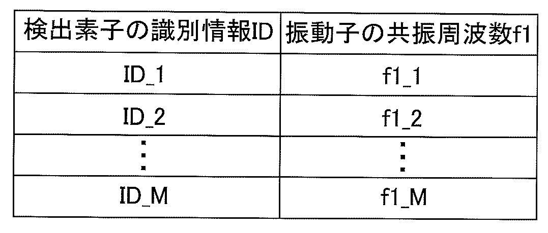
表1において、ID_1~ID_Mは、それぞれ、検出素子3-1~3-Mの識別情報を表わし、f1_1~f1_Mは、それそれ、検出素子3-1~3-Mにおける振動子24の共振周波数(振動子24が検出対象物の影響を受けて振動しているときの共振周波数)を表す。
In Table 1, ID_1 to ID_M respectively represent the identification information of the detection elements 3-1 to 3-M, and f1_1 to f1_M respectively represent the resonant frequency of the
そして、共振周波数f1_1~f1_Mは、それそれ、検出素子3-1~3-Mの識別情報ID_1~ID_Mに対応付けられる。 The resonant frequencies f1_1 to f1_M are then associated with the identification information ID_1 to ID_M of the detection elements 3-1 to 3-M, respectively.
検出回路2は、図18に示すフローチャートを実行して検出対象物Dm_iが検出されたことを検知したとき、表1に示す対応表を参照して、ステップS13において検出した共振周波数f1_i_1~f1_i_kに一致する共振周波数f1(f1_1~f1_Mのいずれか)を検出し、その検出した共振周波数f1(f1_1~f1_Mのいずれか)に対応付けられた検出素子の識別情報ID(ID_1~ID_Mのいずれか)を検出して、検出対象物Dm_iを検出した検出素子(検出素子3-1~3-Mのいずれか)を特定する。また、検出回路2は、共振周波数f1(f1_1~f1_Mのいずれか)に基づいて検出対象物Dm_i(温度およびガス等のいずれか)を特定する。
When the
その結果、M個の検出素子3-1~3-Mを所定の領域内に配置することによって、所定の領域内において少なくとも1つの検出対象物を検出した範囲を特定することができる。 As a result, by arranging M detection elements 3-1 to 3-M within a specified area, it is possible to identify the range within the specified area in which at least one detection object is detected.
また、所定の領域内において少なくとも1つの検出対象物を検出した範囲を特定することを所定の時間間隔で繰り返し実行することによって、所定の領域内において少なくとも1つの検出対象物を検出した範囲が変化したか否かを検出できる。 In addition, by repeatedly identifying the range in which at least one detection object is detected within a specified area at a specified time interval, it is possible to detect whether the range in which at least one detection object is detected within the specified area has changed.
図21は、実施の形態1による別の検出装置の概略図である。実施の形態1による検出装置は、図21に示す検出装置10Aであってもよい。
Figure 21 is a schematic diagram of another detection device according to
図21を参照して、検出装置10Aは、図1に示す検出装置10の送信アンテナ12および受信アンテナ13をアンテナ17に変えたものであり、その他は、図1に示す検出装置10と同じである。
Referring to FIG. 21, the
検出装置10Aにおいて、アンテナ17は、発生回路によって発生された電磁場EWを、一定期間、M個の検出素子3-1~3-Mに無線給電し、一定期間が経過すると、電磁場EWのM個の検出素子3-1~3-Mへの無線給電を停止する。その後、アンテナ17は、M個の検出素子3-1~3-Mから受信信号Rを受信し、その受信した受信信号Rを受信回路へ出力する。
In the
このように、アンテナ17は、送信アンテナ12および受信アンテナ13の両方の機能を果たす1個のアンテナである。
In this way,
検出装置10Aの動作は、図18に示すフローチャートにおいて、ステップS2を「電磁場EWを発生し、その発生した電磁場EWを、アンテナ17によって、一定期間、M個の検出素子3-1~3-Mに無線給電するステップ」に変え、ステップS8を「アンテナ17がM個の受信信号R0_1(t)~R0_M(t)が重畳された受信信号R0_SPM_D(t)と、M個の受信信号R1_1(t)~R1_M(t)が重畳された受信信号R1_SPM_D(t)とを無線によって受信するステップ」に変えたフローチャートに従って実行される。
The operation of the
図22は、実施の形態1における別の検出素子の概略図である。実施の形態1における検出素子は、図22に示す検出素子3-1Bであってもよい。
Figure 22 is a schematic diagram of another detection element in
図22を参照して、検出素子3-1Bは、図2から図4に示す検出素子3-1のアンテナ27,28を削除したものであり、その他は、検出素子3-1と同じである。その結果、検出素子3-1Bは、アンテナ25,26からなる1個のアンテナ部材を有する。
Referring to FIG. 22, detection element 3-1B is the same as detection element 3-1 shown in FIGS. 2 to 4 except that
検出素子3-1Bは、図6から図11に示す製造方法において、図6および図7に示すガラスプロセスにおける工程(A-4)~工程(A-9)を削除して構造物COMP1を作製し、その後、図6および図7に示すガラスプロセスにおける工程(A-1)~工程(A-9)を実行して構造物COMP2を作製する製造方法によって作製される。この場合、構造物COMP1は、工程(A-3)が終了した基板23に送廃液口233を形成した構造からなる。
Detection element 3-1B is produced by a manufacturing method shown in Figures 6 to 11 in which structure COMP1 is produced by eliminating steps (A-4) to (A-9) in the glass process shown in Figures 6 and 7, and then structure COMP2 is produced by carrying out steps (A-1) to (A-9) in the glass process shown in Figures 6 and 7. In this case, structure COMP1 has a structure in which a liquid supply/
検出素子3-1Bにおいては、アンテナ25,26(1個のアンテナ部材)は、一定期間、送受信装置1(または送受信装置1A)から無線給電された電磁場EWを無線によって受信し、その受信した電磁場EWに基づく振動電場Eを振動子24に印加する。その後、アンテナ25,26(1個のアンテナ部材)は、振動子24の振動波形からなる受信信号R0(t),R1(t)を受信し、その受信した受信信号R0(t),R1(t)を無線によって送受信装置1(または送受信装置1A)へ順次送信する。
In the detection element 3-1B, the
なお、検出素子3-1Bは、アンテナ25,26に代えてアンテナ27,28を備えていてもよい。この場合、アンテナ27,28は、1個のアンテナ部材を構成する。つまり、検出素子3-1Bは、アンテナ25,26からなる1個のアンテナ部材と、アンテナ27,28からなる1個のアンテナ部材とのうちのいずれか一方を備えていればよい。
The detection element 3-1B may be equipped with
検出素子3-1Bがアンテナ25,26に代えてアンテナ27,28を備える場合、検出素子3-1Bは、図6から図11に示す製造方法において、図6および図7に示すガラスプロセスを実行して図7に示す構造物COMP1を作製し、その後、図6および図7に示すガラスプロセスにおける工程(A-4)~工程(A-10)を削除して構造物COMP2を作製する製造方法によって作製される。この場合、構造物COMP2は、工程(A-3)に示す“凹部231”および“支持部材232”に代えてそれぞれ“凹部211”および“支持部材212”が形成された基板21からなる。
When the detection element 3-1B has
図1に示す検出装置10のM個の検出素子3-1~3-Mの各々が検出素子3-1Bからなる場合、検出装置10の動作は、図18に示すフローチャートにおいて、ステップS2を「電磁場EWを発生し、その発生した電磁場EWを、送信アンテナ12によって、一定期間、M個の検出素子3-1(3-1B)~3-M(3-1B)に無線給電するステップ」に変え、ステップS3を「アンテナ25,26(またはアンテナ27,28)が電磁場EWを無線によって、一定期間、受信するステップ」に変え、ステップS7を「アンテナ25,26(またはアンテナ27,28)が受信信号R0(t),R1(t)を無線によって送信するステップ」に変えたフローチャートに従って実行される。
When each of the M detection elements 3-1 to 3-M of the
また、図21に示す検出装置10AのM個の検出素子3-1~3-Mの各々が検出素子3-1Bからなる場合、検出装置10Aの動作は、図18に示すフローチャートにおいて、ステップS2を「電磁場EWを発生し、その発生した電磁場EWを、アンテナ17によって、一定期間、M個の検出素子3-1~3-Mに無線給電するステップ」に変え、ステップS3を「アンテナ25,26(またはアンテナ27,28)が電磁場EWを無線によって、一定期間、受信するステップ」に変え、ステップS7を「アンテナ25,26(またはアンテナ27,28)が受信信号R0(t),R1(t)を無線によって送信するステップ」に変え、ステップS8を「アンテナ17が、M個の受信信号R0_1(t)~R0_M(t)が重畳された受信信号R0_SPM_D(t)と、M個の受信信号R1_1(t)~R1_M(t)が重畳された受信信号R1_SPM_D(t)とを無線によって順次受信するステップ」に変えたフローチャートに従って実行される。
In addition, when each of the M detection elements 3-1 to 3-M of the
M個の検出素子3-1~3-MにおけるM個の振動子24のM個の共振周波数が同じである場合の検出装置10の動作について説明する。
The operation of the
この場合、送受信装置1は、発生回路および受信回路に追加して制御回路を備える。制御回路は、検出素子3-1~3-Mの識別情報ID_1~ID_Mと、送受信装置1の位置を基準とした検出素子3-1~3-Mの配置位置の方向θ3-1~θ3-Mとを相互に対応付けた対応表を保持する。検出素子3-1~3-Mの識別情報ID_1~ID_Mと、送受信装置1の位置を基準とした検出素子3-1~3-Mの配置位置の方向θ3-1~θ3-Mとの対応関係を示す対応表を表2に示す。
In this case, the transmitting/
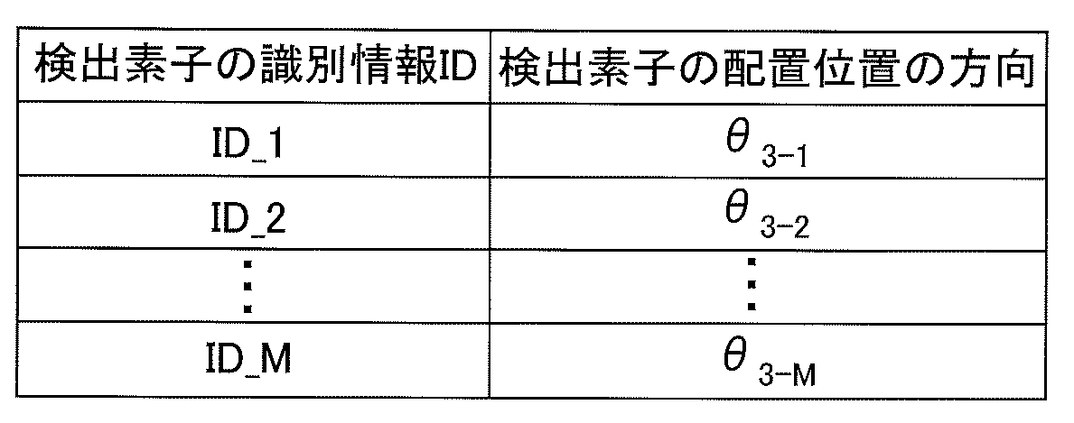
表2において、検出素子3-1~3-Mの配置位置の方向θ3-1~θ3-Mは、それぞれ、検出素子3-1~3-Mの識別情報ID_1~ID_Mに対応付けられる。 In Table 2, the directions θ 3-1 to θ 3- M of the arrangement positions of the detection elements 3-1 to 3- M correspond to the identification information ID_1 to ID_M of the detection elements 3-1 to 3-M, respectively.
送受信装置1の位置を[x1,y1]とし、検出素子3-1の位置を[x3-1,y3-1]とすると、方向θ3-1は、次式によって算出される。
If the position of the transmitting/
θ3-1=tan-1[|y3-1-y1|/|x3-1-x1|]・・・(2)
検出素子3-2~3-Mの位置をそれぞれ[x3-2,y3-2]~[x3-M,y3-M]とすると、式(2)の“x3-1”,“y3-1”に代えてそれぞれ“x3-2”,“y3-2”を式(2)に代入することによって方向θ3-2が算出され、以下、同様にして、式(2)の“x3-1”,“y3-1”に代えてそれぞれ“x3-M”,“y3-M”を式(2)に代入することによって方向θ3-Mが算出される。
θ 3-1 = tan -1 [|y 3-1 -y 1 |/|x 3-1 -x 1 |]...(2)
If the positions of detection elements 3-2 to 3-M are [ x3-2 , y3-2 ] to [ x3-M , y3 -M ], respectively, the direction θ3-2 is calculated by substituting " x3-2 " and " y3-2 " into equation (2) in place of " x3-1 " and " y3-1 " respectively, and similarly, the direction θ3 -M is calculated by substituting "x3 - M " and "y3 - M " into equation (2) in place of "x3-1" and " y3-1 " respectively.
送受信装置1の発生回路は、電磁場EWを発生し、その発生した電磁場EWを搬送波(例えば、1GHzの搬送波)に重畳して送信アンテナ12へ供給する。制御回路は、電磁場EWを検出素子3-1に無線給電する場合、表2に示す対応表を参照して、識別情報ID_1に対応付けられた方向θ3-1に基づいて、電磁場EWが重畳された搬送波を、方向θ3-1を有する指向性の電波によって送信するように送信アンテナ12を制御する。送受信装置1の制御回路は、電磁場EWが重畳された搬送波をそれぞれ検出素子3-2~3-Mへ無線給電する場合も、同様にして、電磁場EWが重畳された搬送波を、それぞれ、方向θ3-2~θ3-Mを有する指向性の電波によって送信するように送信アンテナ12を制御する。
The generating circuit of the transmitting/
なお、指向性を有する電波の送信方法は、周知であるので、その詳細についての説明は、省略する。 The method of transmitting directional radio waves is well known, so a detailed explanation will be omitted.
図23は、図1に示す検出装置10の動作を説明するための別のフローチャートである。なお、図23においては、M個の検出素子3-1~3-Mが送受信装置1の送信アンテナ12によって送信された電磁波EWの到達範囲内に配置されていることを前提とし、M個の検出素子3-1~3-MにおけるM個の振動子24のM個の共振周波数が相互に同じであることを前提とする。
Figure 23 is another flowchart for explaining the operation of the
図23に示すフローチャートは、図18に示すフローチャートのステップS2をステップS21,S22に変え、図18に示すフローチャートのステップS8~S16をステップS23~S28に変えたものであり、その他は、図18に示すフローチャートと同じである。 The flowchart shown in FIG. 23 is the same as the flowchart shown in FIG. 18, except that step S2 in the flowchart shown in FIG. 18 is replaced with steps S21 and S22, and steps S8 to S16 in the flowchart shown in FIG. 18 are replaced with steps S23 to S28.
図23を参照して、検出装置10の動作が開始されると、上述したステップS1が実行され、ステップS1において、タイミングtが、電磁場EWをM個の検出素子3-1~3-Mに無線給電するタイミングTSPであると判定されると、送受信装置1の制御回路は、i=1を設定する(ステップS21)。
Referring to FIG. 23, when the operation of the
そして、発生回路は、電磁場EWを発生し、その発生した電磁場EWを搬送波に重畳して送信アンテナ12へ供給する。制御回路は、表2に示す対応表を参照して、送受信装置1から検出素子3-iへの方向θ3-iに基づいて、電磁場EWが重畳された搬送波を、方向θ3-iを有する指向性の電波によって送信するように送信アンテナ12を制御する。そうすると、送信アンテナ12は、制御回路からの制御に従って、発生回路からの搬送波(電磁場EWが重畳された搬送波)を、方向θ3-iを有する指向性の電波によって検出素子3-iに無線給電する(ステップS22)。
The generating circuit then generates an electromagnetic field EW, superimposes the generated electromagnetic field EW on a carrier wave, and supplies the superimposed electromagnetic field EW to the transmitting antenna 12. The control circuit refers to the correspondence table shown in Table 2, and controls the transmitting antenna 12 based on the direction θ 3-i from the transmitting/
ステップS22の後、検出素子3-iは、図18において説明したステップS3~S7を順次実行する。 After step S22, the detection element 3-i sequentially executes steps S3 to S7 described in FIG. 18.
ステップS7の後、送受信装置1の受信回路は、受信アンテナ13を介して受信信号R0(t)_i,R1(t)_iを無線によって順次受信し(ステップS23)、その受信した受信信号R0(t)_i,R1(t)_iを検出回路2へ出力する。
After step S7, the receiving circuit of the transmitting/
検出回路2は、受信信号R0(t)_i,R1(t)_iを受け、その受けた受信信号R0(t)_iに基づいて共振周波数f0(t)_iを検出し(ステップS24)、受信信号R1(t)_iに基づいて共振周波数f1(t)_iを検出する(ステップS25)。
The
そして、検出回路2は、共振周波数f0(t)_i,f1(t)_iに基づいて共振周波数の変化量Δf(t)_iが時間tに対して低下することを検出することによって検出素子3-iにおいて検出対象物Dm_iが検出されたことを検知する(ステップS26)。
Then, the
その後、検出回路2は、i=Mであるか否かを判定する(ステップS27)。
Then, the
ステップS27において、i=Mでないと判定されたとき、検出回路2は、i=i+1を設定する(ステップS28)。その後、一連の動作は、ステップS22へ移行し、ステップS27において、i=Mであると判定されるまで、ステップS22,S3~S7,S23~ステップS28が繰り返し実行される。
If it is determined in step S27 that i is not equal to M, the
そして、ステップS27において、i=Mであると判定されると判定されると、一連の動作が終了する。 Then, in step S27, if it is determined that i=M, the series of operations ends.
図23に示すフローチャートによれば、電磁場EWを1個の検出素子3-iに無線給電し、1個の検出素子3-iから受信した受信信号R0(t)_i,R1(t)_iに基づいて検出素子3-iにおいて検出対象物Dm_iが検出されたことを検知すること(ステップS24~S26参照)をM個の検出素子3-1~3-Mの全てについて実行するので、M個の検出素子3-1~3-MにおけるM個の振動子24のM個の共振周波数が同じであっても、M個の検出素子3-1~3-Mにおいて同じ検出対象物が検出されたことを遠隔で正確に検知できる。
According to the flowchart shown in FIG. 23, the electromagnetic field EW is wirelessly fed to one detection element 3-i, and detection of the detection object Dm_i in the detection element 3-i is detected based on the reception signals R0(t)_i, R1(t)_i received from the one detection element 3-i (see steps S24 to S26) is performed for all M detection elements 3-1 to 3-M. Therefore, even if the M resonant frequencies of the
そして、M個の検出素子3-1~3-Mを所定の領域内に配置することによって所定の領域内において1個の検出対象物を検出した範囲を特定することができる。 By arranging M detection elements 3-1 to 3-M within a specified area, it is possible to identify the range within the specified area in which a single detection target is detected.
また、所定の領域内において1個の検出対象物を検出した範囲を特定することを所定の時間間隔で繰り返し実行することによって、所定の領域内において1個の検出対象物を検出した範囲が変化したか否かを検出できる。 In addition, by repeatedly identifying the range in which a single detection target is detected within a specified area at a specified time interval, it is possible to detect whether the range in which a single detection target is detected within a specified area has changed.
検出装置10Aの動作は、図23に示すフローチャートにおいて、ステップS22を「電磁場EWを発生し、アンテナ17が、発生回路からの電磁場EWが重畳された搬送波を、方向θ3-iを有する指向性の電波によって、一定の期間、検出素子3-iに無線給電するステップ」に変え、ステップS23を「アンテナ17が受信信号R0(t)_i,R1(t)_iを無線によって順次受信するステップ」に変えたフローチャートに従って実行される。
The operation of the
図1に示す検出装置10のM個の検出素子3-1~3-Mの各々が検出素子3-1Bからなる場合、検出装置10の動作は、図23に示すフローチャートにおいて、ステップS22を「電磁場EWを発生し、その発生した電磁場EWが重畳された搬送波を、方向θ3-iを有する指向性の電波によって、一定期間、検出素子3-iに無線給電するステップ」に変え、ステップS3を「アンテナ25,26(またはアンテナ27,28)が搬送波(電磁場EWが重畳された搬送波)を無線によって、一定期間、受信するステップ」に変え、ステップS7を「アンテナ25,26(またはアンテナ27,28)が受信信号R0(t)_i,R1(t)_iを無線によって送信するステップ」に変えたフローチャートに従って実行される。
When each of the M detection elements 3-1 to 3-M of the
また、図21に示す検出装置10AのM個の検出素子3-1~3-Mの各々が検出素子3-1Bからなる場合、検出装置10Aの動作は、図23に示すフローチャートにおいて、ステップS22を「電磁場EWを発生し、アンテナ17が、発生回路からの電磁場EWが重畳された搬送波を、方向θ3-iを有する指向性の電波によって、一定期間、検出素子3-iに無線給電するステップ」に変え、ステップS3を「アンテナ25,26(またはアンテナ27,28)が搬送波(電磁場EWが重畳された搬送波)を無線によって、一定期間、受信するステップ」に変え、ステップS7を「アンテナ25,26(またはアンテナ27,28)が受信信号R0(t)_i,R1(t)_iを無線によって送信するステップ」に変え、ステップS23を「アンテナ17が受信信号R0(t)_i,R1(t)_iを無線によって受信するステップ」に変えたフローチャートに従って実行される。
21, when each of the M detection elements 3-1 to 3-M of the
図23に示すフローチャートについてのその他の説明は、図18に示すフローチャートについての説明と同じである。 The rest of the explanation for the flowchart shown in FIG. 23 is the same as the explanation for the flowchart shown in FIG. 18.
図24は、実施の形態1による検出対象物の検出方法を示すフローチャートである。図24を参照して、検出対象物の検出が開始されると、送受信装置1は、電磁場EWをM個の検出素子3-1~3-Mに無線給電する(ステップS51)。
Figure 24 is a flowchart showing a method for detecting an object to be detected according to
そして、送受信装置1は、M個の検出素子3-1~3-MにおけるM個の振動子24の電場E(電磁場EWに基づいた電場)のみに起因した振動波形からなる受信信号R0_SPM_D(t)を無線によってM個の検出素子3-1~3-Mから受信する(ステップS52)。
Then, the transmission/
また、送受信装置1は、M個の検出素子3-1~3-MにおけるM個の振動子24の検出対象物の影響を受けて振動するときの振動波形からなる受信信号R1_SPM_D(t)を無線によってM個の検出素子3-1~3-Mから受信する(ステップS53)。
The transmitter/
そうすると、検出回路2は、受信信号R0_SPM_D(t)に基づいてM個の検出素子3-1~3-MのM個の振動子24のM個の共振周波数f0(t)_1~f0(t)_Mを検出する(ステップS54)。
Then, the
引き続いて、検出回路2は、受信信号R1_SPM_D(t)に基づいてM個の検出素子3-1~3-MのM個の振動子24のM個の共振周波数f1(t)_1~f1(t)_Mを検出する(ステップS55)。
Then, the
そして、検出回路2は、M個の共振周波数f0(t)_1~f0(t)_MおよびM個の共振周波数f1(t)_1~f1(t)_Mに基づいて、共振周波数の変化量Δf(t)_1~Δf(t)_Mが時間tに対して低下することを検出することによってM個の検出素子3-1~3-Mにおいて検出対象物が検出されたことを検知する(ステップS56)。
Then, based on the M resonant frequencies f0(t)_1 to f0(t)_M and the M resonant frequencies f1(t)_1 to f1(t)_M, the
これによって、検出対象物の検出が終了する。 This completes the detection of the object to be detected.
図24に示す検出対象物の検出方法において、ステップS51における電磁場EWのM個の検出素子3-1~3-Mへの無線給電は、図18に示すフローチャートのステップS2を実行することによって実現される。 In the method for detecting an object to be detected shown in FIG. 24, the wireless power supply to the M detection elements 3-1 to 3-M of the electromagnetic field EW in step S51 is realized by executing step S2 of the flowchart shown in FIG. 18.
また、図24に示す検出対象物の検出方法において、ステップS52における受信信号R0_SPM_D(t)の無線によるM個の検出素子3-1~3-Mからの受信は、図18に示すフローチャートのステップS8を実行することによって実現される。 In addition, in the method for detecting an object to be detected shown in FIG. 24, the wireless reception of the received signal R0_SPM_D(t) from M detection elements 3-1 to 3-M in step S52 is realized by executing step S8 in the flowchart shown in FIG. 18.
更に、図24に示す検出対象物の検出方法において、ステップS53における受信信号R1_SPM_D(t)の無線によるM個の検出素子3-1~3-Mからの受信は、図18に示すフローチャートのステップS8を実行することによって実現される。 Furthermore, in the method for detecting an object to be detected shown in FIG. 24, the wireless reception of the received signal R1_SPM_D(t) from M detection elements 3-1 to 3-M in step S53 is realized by executing step S8 in the flowchart shown in FIG. 18.
更に、図24に示す検出対象物の検出方法において、ステップS54におけるM個の共振周波数f0(t)_1~f0(t)_Mの検出は、図18に示すフローチャートのステップS12をi=1~Mの全てについて実行することによって実現され、ステップS55におけるM個の共振周波数f1(t)_1~f1(t)_Mの検出は、図18に示すフローチャートのステップS13をi=1~Mの全てについて実行することによって実現され、ステップS56における「M個の検出素子3-1~3-Mにおいて検出対象物が検出されたことを検知すること」は、図18に示すフローチャートのステップS14をi=1~Mの全てについて実行することによって実現される。 Furthermore, in the method for detecting an object to be detected shown in FIG. 24, the detection of M resonant frequencies f0(t)_1 to f0(t)_M in step S54 is realized by executing step S12 of the flowchart shown in FIG. 18 for all i=1 to M, the detection of M resonant frequencies f1(t)_1 to f1(t)_M in step S55 is realized by executing step S13 of the flowchart shown in FIG. 18 for all i=1 to M, and "detecting that an object to be detected has been detected in M detection elements 3-1 to 3-M" in step S56 is realized by executing step S14 of the flowchart shown in FIG. 18 for all i=1 to M.
また、図24に示す検出対象物の検出方法においては、指向性の電波を用いて電磁場EWをM個の検出素子3-1~3-Mへ無線給電してもよい。 In addition, in the method for detecting an object to be detected shown in FIG. 24, the electromagnetic field EW may be wirelessly fed to M detection elements 3-1 to 3-M using directional radio waves.
この場合、ステップS51において、送受信装置1は、指向性の電波によって搬送波(電磁場EWが重畳された搬送波)を1個の検出素子3-iに無線給電することをM個の検出素子3-1~3-Mの全てについて実行する。このとき、指向性の電波によって搬送波(電磁場EWが重畳された搬送波)を1個の検出素子3-iに無線給電することをM個の検出素子3-1~3-Mの全てについて実行することは、図23に示すフローチャートのステップS22をi=1~Mの全てについて実行することによって実現される。
In this case, in step S51, the transmission/
また、ステップS52において、送受信装置1は、受信信号R0_SPM_D(t)に代えて、M個の検出素子3-1~3-MからM個の受信信号R0(t)_1~R0(t)_Mを無線によって受信する。この時、ステップS52におけるM個の受信信号R0(t)_1~R0(t)_Mの受信は、図23に示すフローチャートのステップS23をi=1~Mの全てについて実行することによって実現される。
In addition, in step S52, the
更に、ステップS53において、送受信装置1は、受信信号R1_SPM_D(t)に代えて、M個の検出素子3-1~3-MからM個の受信信号R1(t)_1~R1(t)_Mを無線によって受信する。この時、ステップS53におけるM個の受信信号R1(t)_1~R1(t)_Mの受信は、図23に示すフローチャートのステップS23をi=1~Mの全てについて実行することによって実現される。
Furthermore, in step S53, the
更に、ステップS54において、検出回路2は、受信信号R0_SPM_D(t)に代えて、M個の検出素子3-1~3-MからのM個の受信信号R0(t)_1~R0(t)_Mに基づいて、M個の共振周波数f0(t)_1~f0(t)_Mを検出する。この時、ステップS54におけるM個の共振周波数f0(t)_1~f0(t)_Mの検出は、図23に示すフローチャートのステップS24をi=1~Mの全てについて実行することによって実現される。
Furthermore, in step S54, the
更に、ステップS55において、検出回路2は、受信信号R1_SPM_D(t)に代えて、M個の検出素子3-1~3-MからのM個の受信信号R1(t)_1~R1(t)_Mに基づいて、M個の共振周波数f1(t)_1~f1(t)_Mを検出する。この時、ステップS55におけるM個の共振周波数f1(t)_1~f1(t)_Mの検出は、図23に示すフローチャートのステップS25をi=1~Mの全てについて実行することによって実現される。
Furthermore, in step S55, the
更に、ステップS56において、M個の共振周波数f0(t)_1~f0(t)_MおよびM個の共振周波数f1(t)_1~f1(t)_Mに基づいて、共振周波数の変化量Δf(t)_1~Δf(t)_Mが時間tに対して低下することを検出することによってM個の検出素子3-1~3-Mにおいて検出対象物が検出されたことを検知することは、図23に示すフローチャートのステップS26をi=1~Mの全てについて実行することによって実現される。 Furthermore, in step S56, based on the M resonant frequencies f0(t)_1 to f0(t)_M and the M resonant frequencies f1(t)_1 to f1(t)_M, the amount of change in the resonant frequencies Δf(t)_1 to Δf(t)_M is detected over time t, thereby detecting that the object to be detected has been detected in the M detection elements 3-1 to 3-M, by executing step S26 of the flowchart shown in FIG. 23 for all of i = 1 to M.
従って、図24に示す検出対象物の検出方法は、上述した実施の形態1における説明に基づいた検出方法である。
Therefore, the detection method for the detection target shown in FIG. 24 is a detection method based on the explanation in the above-mentioned
なお、実施の形態1においては、検出素子3-1~3-Mの各々において、基板21は、複数の支持部材212を有し、基板23は、複数の支持部材232を有するが、複数の支持部材212は、少なくとも1個が金属からなっていればよく、複数の支持部材232は、少なくとも1個が金属からなっていればよい。複数の支持部材212の少なくとも1個が金属からなっていれば、アンテナ26を電気的にアンテナ25に接続でき、複数の支持部材232の少なくとも1個が金属からなっていれば、アンテナ28を電気的にアンテナ27に接続できるからである。
In the first embodiment, in each of the detection elements 3-1 to 3-M, the
また、支持部材212および支持部材232の各々は、円柱形状に限らず、三角柱、四角柱、および五角柱等の形状を有していてもよく、長さ方向に垂直な方向における断面形状は、任意の形状からなっていてもよい。
In addition, each of the
更に、空間部SPおよび振動子24の平面形状は、流線形に限らず、楕円形状であってもよい。
Furthermore, the planar shape of the space SP and the
[実施の形態2]
図25は、実施の形態2による検出装置の概略図である。図25を参照して、実施の形態2による検出装置10Bは、図1に示す検出装置10のM個の検出素子3-1~3-MをM個の検出素子4-1~4-Mに変えたものであり、その他は、検出装置10と同じである。M個の検出素子4-1~4-Mの各々は、複数の振動子24を含む。
[Embodiment 2]
Fig. 25 is a schematic diagram of a detection device according to
図26は、図25に示す検出素子4-1の概略図である。なお、図26は、複数の振動子24が3個の振動子24である場合について検出素子4-1の概略図を示す。
Figure 26 is a schematic diagram of the detection element 4-1 shown in Figure 25. Note that Figure 26 shows a schematic diagram of the detection element 4-1 in the case where the
図26を参照して、検出素子4-1は、素子ユニットUnit_1~Unit_3と基台400とを含む。素子ユニットUnit_1~Unit_3は、所定の間隔で基台400上に固定される。素子ユニットUnit_1~Unit_3の各々は、図2から図4に示す検出素子3-1と同じ構成からなる。
Referring to FIG. 26, the detection element 4-1 includes element units Unit_1 to Unit_3 and a
その結果、検出素子4-1は、素子ユニットUnit_1~Unit_3を基台400上に所定の間隔で一列に配列した構成からなる。
As a result, the detection element 4-1 is configured by arranging element units Unit_1 to Unit_3 in a row at a predetermined interval on the
検出素子4-1において、素子ユニットUnit_1~Unit_3に含まれる3個の振動子24は、相互に異なる共振周波数(即ち、例えば、相互に異なる厚み)を有する。
In the detection element 4-1, the three
図25に示す検出素子4-2~4-Mの各々も、図26に示す検出素子4-1と同じ構成からなる。 Each of the detection elements 4-2 to 4-M shown in FIG. 25 has the same configuration as the detection element 4-1 shown in FIG. 26.
図27は、素子ユニットの配列構造を示す概略図である。図27を参照して、検出素子4-1がp×q(p,qの一方は、2以上の整数であり、p,qの他方は、1以上の整数である)個の素子ユニットUnit_11~Unit_pqを含む場合、p×q個の素子ユニットUnit_11~Unit_pqは、p行q列の行列状に配置される。そして、検出素子4-2~4-Mの各々も、検出素子4-1と同じようにp行q列の行列状に配置されたp×q個の素子ユニットUnit_11~Unit_pqを含む。 Figure 27 is a schematic diagram showing the arrangement of element units. With reference to Figure 27, when detection element 4-1 includes p x q element units Unit_11 to Unit_pq (one of p and q is an integer of 2 or more, and the other of p and q is an integer of 1 or more), the p x q element units Unit_11 to Unit_pq are arranged in a matrix of p rows and q columns. Similarly to detection element 4-1, each of detection elements 4-2 to 4-M also includes p x q element units Unit_11 to Unit_pq arranged in a matrix of p rows and q columns.
検出素子4-1~4-Mの各々において、p×q個の素子ユニットUnit_11~Unit_pqにおけるp×q個の振動子24は、相互に異なる共振周波数(即ち、例えば、相互に異なる厚み)を有する。
In each of the detection elements 4-1 to 4-M, the p×
このように、検出素子4-1~4-Mにおいては、複数の素子ユニットUnitは、列状に配列されていてもよく、行列状に配列されていてもよい。 In this way, in the detection elements 4-1 to 4-M, the multiple element units Unit may be arranged in a row or in a matrix.
そして、検出素子4-1~4-Mの各々に含まれる振動子24の個数は、検出対象物の種類の総数以下である。
The number of
また、検出素子4-1~4-Mは、相互に同じ個数の振動子24(即ち、相互に同じ個数の素子ユニットUnit)を備えていてもよく、相互に異なる個数の振動子24(即ち、相互に異なる個数の素子ユニットUnit)を備えていてもよい。 Furthermore, the detection elements 4-1 to 4-M may each have the same number of transducers 24 (i.e., the same number of element units), or may each have a different number of transducers 24 (i.e., a different number of element units).
検出素子4-1~4-Mが相互に同じ個数の振動子24(即ち、相互に同じ個数の素子ユニットUnit)を備える場合、検出装置10Bは、検出素子4-1~4-Mを用いて個数および種類が相互に同じである検出対象物を検出し、または検出素子4-1~4-Mを用いて個数が相互に同じであり、かつ、種類が相互に異なる検出対象物を検出する。
When the detection elements 4-1 to 4-M have the same number of transducers 24 (i.e., the same number of element units), the
個数および種類が相互に同じである検出対象物を検出するとき、M個の検出素子4-1~4-Mは、M個の検出素子4-1~4-Mにおいて相互に同じ個数および相互に同じ共振周波数の振動子24を含む。一方、個数が相互に同じであり、かつ、種類が相互に異なる検出対象物を検出するとき、M個の検出素子4-1~4-Mは、M個の検出素子4-1~4-Mにおいて個数が相互に同じであり、かつ、共振周波数が相互に少なくとも1つ異なる振動子24を含む。
When detecting objects that are the same in number and type, the M detection elements 4-1 to 4-M include the same number of
図28は、図25に示す検出装置10Bの動作を説明するためのフローチャートである。なお、図28においては、M個の検出素子4-1~4-Mが送受信装置1の送信アンテナ12によって送信された電磁場EWの到達範囲内に配置されていることを前提とする。
Figure 28 is a flowchart for explaining the operation of the
図28に示すフローチャートは、図23に示すフローチャートのステップS4~ステップS7をそれぞれステップS4A~ステップS7Aに変え、図23に示すフローチャートのステップS23~ステップS26をステップS23A,S24Aに変えたものであり、その他は、図23に示すフローチャートと同じである。 The flowchart shown in FIG. 28 is the same as the flowchart shown in FIG. 23, except that steps S4 to S7 of the flowchart shown in FIG. 23 are replaced with steps S4A to S7A, and steps S23 to S26 of the flowchart shown in FIG. 23 are replaced with steps S23A and S24A.
図28を参照して、検出装置10Bの動作が開始されると、上述したステップS1,S21,S22,S3が順次実行される。なお、実施の形態2においては、ステップS22において、「電磁場EWが重畳された搬送波は、検出素子4-iに無線給電される」ことになる。
Referring to FIG. 28, when the operation of the
そして、ステップS3の後、検出素子4-iにおいて、アンテナ25,26(またはアンテナ27,28)は、電磁場EWに基づいた振動電場Eを複数の振動子24に印加する(ステップS4A)。
Then, after step S3, in the detection element 4-i, the
その後、検出素子4-iにおいて、アンテナ27,28(またはアンテナ25,26)は、複数の振動子24の振動波形からなる複数の受信信号R0_1(t)~R0_jmax(t)が重畳された受信信号R0_SPM_SC(t)_iを複数の振動子24から受信する(ステップS5A)。
Thereafter, in the detection element 4-i, the
引き続いて、検出素子4-iにおいて、アンテナ27,28(またはアンテナ25,26)は、複数の振動子24の振動波形からなる複数の受信信号R1_1(t)~R1_jmax(t)が重畳された受信信号R1_SPM_SC(t)_iを複数の振動子24から受信する(ステップS6A)。
Subsequently, in the detection element 4-i, the
そうすると、検出素子4-iにおいて、アンテナ27,28(またはアンテナ25,26)は、受信信号R0_SPM_SC(t)_i,R1_SPM_SC(t)_iを無線によって送信する(ステップS7A)。
Then, in the detection element 4-i, the
送受信装置1の受信回路は、受信アンテナ13を介して、受信信号R0_SPM_SC(t)_i,R1_SPM_SC(t)_iを無線によって受信し(ステップS23A)、その受信した受信信号R0_SPM_SC(t)_i,R1_SPM_SC(t)_iを検出回路2へ出力する。
The receiving circuit of the transmitting/
検出回路2は、受信信号R0_SPM_SC(t)_i,R1_SPM_SC(t)_iを受信回路から受け、その受けた受信信号R0_SPM_SC(t)_i,R1_SPM_SC(t)_iに基づいて複数の共振周波数の変化量{Δf_1~Δf_jmax}_iを検出して複数の検出対象物{Dm_1~Dm_jmax}_iを検出する(ステップS24A)。
The
その後、上述したステップS27が実行され、ステップS27において、i=Mでないと判定されたとき、ステップS27において、i=Mであると判定されるまで、ステップS22,S3,S4A~7A,S23A,S24A,S27,S28が繰り返し実行される。 Then, step S27 described above is executed, and if it is determined in step S27 that i=M is not satisfied, steps S22, S3, S4A-7A, S23A, S24A, S27, and S28 are repeatedly executed until it is determined in step S27 that i=M is satisfied.
そして、ステップS27において、i=Mであると判定されると、一連の動作が終了する。 Then, in step S27, when it is determined that i=M, the series of operations ends.
図29は、図28のステップS24Aの詳細な動作を説明するためのフローチャートである。 Figure 29 is a flowchart explaining the detailed operation of step S24A in Figure 28.
図29を参照して、図28のステップS23Aの後、検出回路2は、受信信号R0_SPM_SC(t)_iを1個の時間においてフーリエ変換して周波数成分R0_1(f)_i~R0_jmax(f)_iを取得する(ステップS31)。
29, after step S23A in FIG. 28,
そして、検出回路2は、受信信号R0_SPM_SC(t)_iをk個の時間t1~tkにおいてフーリエ変換して周波数成分{R1_1(f)_i~R1_jmax(f)_i}_1~{R1_1(f)_i~R1_jmax(f)_i}_kを取得する(ステップS32)。
Then,
その後、検出回路2は、j=1を設定し(ステップS33)、周波数成分{R0_j(f)_iに基づいて共振周波数f0_j_iを検出する(ステップS34)。
Then, the
引き続いて、検出回路2は、周波数成分{R1_j(f)_i}_1~{R1_j(f)_i}_kに基づいてそれぞれ共振周波数{f1_j_i}_1~{f1_j_i}_kを検出する(ステップS35)。
Then, the
そうすると、検出回路2は、図18のステップS14において説明した方法によって、共振周波数f0_j_iおよび共振周波数{f1_j_i}_1~{f1_j_i}_kに基づいて共振周波数の変化量Δf_j_iが時間tに対して低下することを検出することによって検出素子4-iにおいて検出対象物Dm_j_iが検出されたことを検知する(ステップS36)。
Then, the
そして、検出回路2は、j=jmaxであるか否かを判定する(ステップS37)。ステップS37において、j=jmaxでないと判定されたとき、検出回路2は、j=j+1を設定する(ステップS38)。その後、一連の動作は、ステップS34へ移行し、ステップS37において、j=jmaxであると判定されるまで、ステップS34~ステップS38が繰り返し実行される。そして、ステップS37において、j=jmaxであると判定されると、一連の動作は、図28のステップS27へ移行する。
Then, the
図29に示すフローチャートにおいて、ステップS34~S36がj=1~jmaxの全てについて実行されることによって、検出素子4-iにおけるjmax個の共振周波数の変化量Δf_1_i~Δf_jmax_iが検出される。従って、jmax個の共振周波数の変化量Δf_1_i~Δf_jmax_iは、図28に示すフローチャートのステップS24Aにおける複数の変化量{Δf_1~Δf_jmax}_iに等しい。 In the flowchart shown in Fig. 29, steps S34 to S36 are executed for all j = 1 to j max , thereby detecting j max amounts of change Δf_1_i to Δf_j max _i in the resonant frequency of the detection element 4-i. Therefore, the j max amounts of change Δf_1_i to Δf_j max _i in the resonant frequency are equal to the multiple amounts of change {Δf_1 to Δf_j max }_i in step S24A of the flowchart shown in Fig. 28.
図30は、受信信号R0_SPM_SC(t),R1_SPM_SC(t)を示す概念図である。また、図31は、受信信号R0_SPM_SC(t),R1_SPM_SC(t)をフーリエ変換したときの周波数成分を示す概念図である。 Figure 30 is a conceptual diagram showing the received signals R0_SPM_SC(t) and R1_SPM_SC(t). Also, Figure 31 is a conceptual diagram showing the frequency components when the received signals R0_SPM_SC(t) and R1_SPM_SC(t) are Fourier transformed.
なお、図30および図31は、1個の検出素子4-iにおける受信信号R0_SPM_SC(t),R1_SPM_SC(t)および受信信号R0_SPM_SC(t),R1_SPM_SC(t)をフーリエ変換したときの周波数成分を示す。また、図31において、k個の時間t1~tkのkをk=4とする。 30 and 31 show the frequency components obtained by Fourier transforming the received signals R0_SPM_SC(t) and R1_SPM_SC(t) in one detection element 4-i and the received signals R0_SPM_SC(t) and R1_SPM_SC(t). In addition, in FIG. 31, k in k times t 1 to t k is k=4.
図30を参照して、受信信号R0_SPM_SC(t)は、1個の検出素子4-iにおいて、時間tに対して、jmax個の振動子24が振動電場Eのみに起因して振動しているときのjmax個の振動子24からの受信信号R0_1(t)~R0_jmax(t)が重畳された振動波形からなる。 Referring to FIG. 30, in one detection element 4-i, the reception signal R0_SPM_SC(t) is composed of a vibration waveform in which reception signals R0_1(t) to R0_j max (t) from j max transducers 24 are superimposed when the j max transducers 24 are vibrating due only to the vibration electric field E for a time t.
また、受信信号R1_SPM_SC(t)は、1個の検出素子4―iにおいて、時間tに対して、jmax個の振動子24が検出対象物の影響を受けて振動しているときのjmax個の振動子24からの受信信号R1_1(t)~R1_jmax(t)が重畳された振動波形からなる。 Furthermore, the reception signal R1_SPM_SC(t) is composed of a vibration waveform in which reception signals R1_1(t) to R1_j max (t) from j max transducers 24 are superimposed when the j max transducers 24 are vibrating under the influence of the detection object for a time t in one detection element 4-i.
そして、1個の時間t0において、受信信号R0_SPM_SC(t)をフーリエ変換すると、図31に示すjmax個の周波数成分R0_1(f)_i,R0_2(f)_i,・・・,R0_jmax(f)_iが得られる。 Then, when the received signal R0_SPM_SC(t) is Fourier transformed at one time t0 , jmax frequency components R0_1(f)_i, R0_2(f)_i, . . . , R0_jmax (f)_i shown in FIG. 31 are obtained.
R0_1(f)_i,R0_2(f)_i,・・・,R0_jmax(f)_iの各部の説明を表3に示す。 Table 3 shows an explanation of each part of R0_1(f)_i, R0_2(f)_i, . . . , R0_jmax (f)_i.
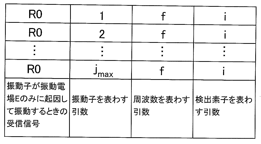
また、k個の時間t1~tkにおいて、受信信号R1_SPM_SC(t)をフーリエ変換すると、図31に示すk(=4)個の周波数成分R1_1(f)_i_1~R1_1(f)_i_2,・・・,R1_1(f)_i_k;R1_2(f)_i_1~R1_2(f)_i_2,・・・,R1_2(f)_i_k;・・・;R1_jmax(f)_i_1~R1_jmax(f)_i_2,・・・,R1_jmax(f)_i_kが得られる。 Furthermore, when the received signal R1_SPM_SC(t) is Fourier transformed at k times t1 to tk , k (=4) frequency components R1_1(f)_i_1 to R1_1(f)_i_2, ..., R1_1(f)_i_k; R1_2(f)_i_1 to R1_2(f)_i_2, ..., R1_2(f)_i_k; ...; R1_j max (f)_i_1 to R1_j max (f)_i_2, ..., R1_j max (f)_i_k shown in Figure 31 are obtained.
R1_1(f)_i_1~R1_1(f)_i_2,・・・,R1_1(f)_i_kの各部の説明を表4に示す。 Table 4 shows the explanation of each part of R1_1(f)_i_1 to R1_1(f)_i_2, ..., R1_1(f)_i_k.
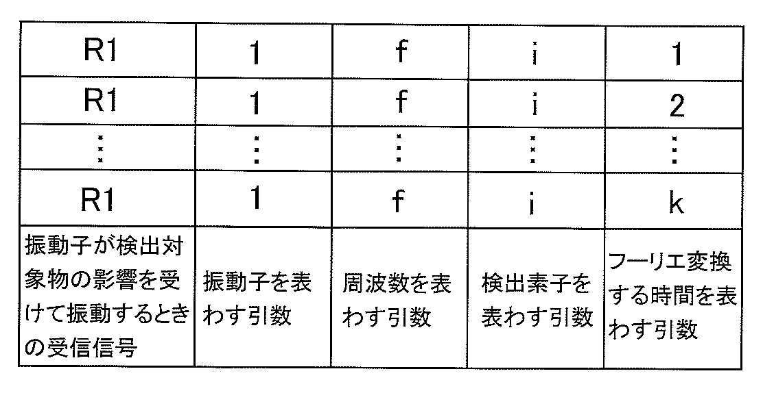
なお、R1_2(f)_i_1~R1_2(f)_i_2,・・・,R1_2(f)_i_k;・・・;R1_jmax(f)_i_1~R1_jmax(f)_i_2,・・・,R1_jmax(f)_i_kの各部の説明も、表4に示す通りである。 Note that the explanation of each part of R1_2(f)_i_1 to R1_2(f)_i_2, ..., R1_2(f)_i_k; ...; R1_j max (f)_i_1 to R1_j max (f)_i_2, ..., R1_j max (f)_i_k is also as shown in Table 4.
そして、周波数成分R0_1(f)_iに基づいて、周波数成分R0_1(f)_iの振幅が最大になるときの周波数が検出素子4-iにおける1番目の振動子24の共振周波数f0_1_iとして検出され、周波数成分R0_2(f)_iに基づいて、周波数成分R0_2(f)_iの振幅が最大になるときの周波数が検出素子4-iにおける2番目の振動子24の共振周波数f0_2_iとして検出され、以下、同様にして、周波数成分R0_jmax(f)_iに基づいて、周波数成分R0_jmax(f)_iの振幅が最大になるときの周波数が検出素子4-iにおけるjmax番目の振動子24の共振周波数f0_jmax_iとして検出される(図31参照)。
Then, based on the frequency component R0_1(f)_i, the frequency when the amplitude of the frequency component R0_1(f)_i is maximum is detected as the resonant frequency f0_1_i of the
また、周波数成分R1_1(f)_i_1に基づいて、周波数成分R1_1(f)_i_1の振幅が最大になるときの周波数が検出素子4-iにおける1番目の振動子24の時間t1における共振周波数f1_1_i_1として検出され、周波数成分R1_1(f)_i_2に基づいて、周波数成分R1_1(f)_i_2の振幅が最大になるときの周波数が検出素子4-iにおける1番目の振動子24の時間t2における共振周波数f1_1_i_2として検出され、以下、同様にして、周波数成分R1_1(f)_i_kに基づいて、周波数成分R1_1(f)_i_kの振幅が最大になるときの周波数が検出素子4-iにおける1番目の振動子24の時間tkにおける共振周波数f1_1_i_kとして検出される(図31参照)。
Furthermore, based on the frequency component R1_1(f)_i_1, the frequency when the amplitude of the frequency component R1_1(f)_i_1 is maximum is detected as the resonant frequency f1_1_i_1 of the
更に、周波数成分R1_2(f)_i_1に基づいて、周波数成分R1_2(f)_i_1の振幅が最大になるときの周波数が検出素子4-iにおける2番目の振動子24の時間t1における共振周波数f1_2_i_1として検出され、周波数成分R1_2(f)_i_2に基づいて、周波数成分R1_2(f)_i_2の振幅が最大になるときの周波数が検出素子4-iにおける2番目の振動子24の時間t2における共振周波数f1_2_i_2として検出され、以下、同様にして、周波数成分R1_2(f)_i_kに基づいて、周波数成分R1_2(f)_i_kの振幅が最大になるときの周波数が検出素子4-iにおける2番目の振動子24の時間tkにおける共振周波数f1_2_i_kとして検出される(図31参照)。
Furthermore, based on the frequency component R1_2(f)_i_1, the frequency when the amplitude of the frequency component R1_2(f)_i_1 is maximum is detected as the resonant frequency f1_2_i_1 of the
以下、同様にして、周波数成分R1_jmax(f)_i_1に基づいて、周波数成分R1_jmax(f)_i_1の振幅が最大になるときの周波数が検出素子4-iにおけるjmax番目の振動子24の時間t1における共振周波数f1_jmax_i_1として検出され、周波数成分R1_jmax(f)_i_2に基づいて、周波数成分R1_jmax(f)_i_2の振幅が最大になるときの周波数が検出素子4-iにおけるjmax番目の振動子24の時間t2における共振周波数f1_jmax_i_2として検出され、以下、同様にして、周波数成分R1_jmax(f)_i_kに基づいて、周波数成分R1_jmax(f)_i_kの振幅が最大になるときの周波数が検出素子4-iにおけるjmax番目の振動子24の時間tkにおける共振周波数f1_jmax_i_kとして検出される(図31参照)。
Thereafter, in a similar manner, based on the frequency component R1_jmax (f)_i_1, the frequency at which the amplitude of the frequency component R1_jmax (f)_i_1 is maximized is detected as the resonant frequency f1_jmax_i_1 of the jmax -
そうすると、共振周波数f0_1_iから共振周波数f1_1_i_1~f1_1_i_kを減算することによって、検出素子4-iにおける1番目の振動子24における共振周波数の変化量Δf_1_iが検出され、共振周波数f0_2_iから共振周波数f1_2_i_1~f1_2_i_kを減算することによって、検出素子4-iにおける2番目の振動子24における共振周波数の変化量Δf_2_iが検出され、以下、同様にして、共振周波数f0_jmax_iから共振周波数f1_jmax_i_1~f1_jmax_i_kを減算することによって、検出素子4-iにおけるjmax番目の振動子24における共振周波数の変化量Δf_jmax_iが検出される(図31参照)。
Then, by subtracting the resonant frequencies f1_1_i_1 to f1_1_i_k from the resonant frequency f0_1_i, the amount of change Δf_1_i in the resonant frequency of the
そして、共振周波数の変化量Δf_1_i,Δf_2_i,・・・,Δf_jmax_iが時間tに対して低下していることを検出することによって、それぞれ、検出素子4-iにおける1番目の振動子24、2番目の振動子24、・・・、jmax番目の振動子24が検出対象物を検出したことが検知される(図28のステップS24A(=図29に示すフローチャート)参照)。
Then, by detecting that the amounts of change in resonant frequency Δf_1_i, Δf_2_i, ..., Δf_j max _i decrease with time t, it is detected that the
上述した図28に示すフローチャート(図29に示すフローチャートを含む)によれば、ステップS27において、i=Mであると判定されるまで、ステップS22,S3,S4A~S7A,S23A,S24A,S27,S28を繰り返し実行することによって、M個の検出素子4-1~4-Mの各々において、jmax個の振動子24によって、相互に異なるjmax個の検出対象物が検出される。
According to the flowchart shown in FIG. 28 (including the flowchart shown in FIG. 29) described above, by repeatedly executing steps S22, S3, S4A to S7A, S23A, S24A, S27, and S28 until it is determined in step S27 that i=M,
この場合、M個の検出素子4-1~4-Mの各々が、共振周波数f0_1,f1_1を有する振動子24(j=1)と、共振周波数f0_2,f1_2を有する振動子24(j=2)と、共振周波数f0_3,f1_3を有する振動子24(j=jmax(=3))とのjmax(=3)個の振動子24を備え、f0_1=f0_2=f0_3およびf1_1=f1_2=f1_3である場合、M個の検出素子4-1~4-Mにおいて、jmax(=3)個の振動子24の共振周波数f0,f1が相互に同じであるので、M個の検出素子4-1~4-Mの各々は、同じ3種類の検出対象物を検出する。そして、M個の検出素子4-1~4-Mの各々において検出される検出対象物の種類の個数は、3個に限らず、2個以上であればよい。
In this case, each of the M detection elements 4-1 to 4-M includes a vibrator 24 (j=1) having a resonant frequency f0_1, f1_1, a vibrator 24 (j=2) having a resonant frequency f0_2, f1_2, and a vibrator 24 (j= jmax (=3)) having a resonant frequency f0_3, f1_3, i.e., jmax (=3)
また、例えば、M=3として、検出素子4-1が共振周波数f0_1,f1_1を有する振動子24(j=1)と、共振周波数f0_2,f1_2を有する振動子24(jmax=2)とのjmax(=2)個の振動子24を備え、検出素子4-2が共振周波数f0_3,f1_3を有する振動子24(j=1)と、共振周波数f0_4,f1_4を有する振動子24(jmax=2)とのjmax(=2)個の振動子24を備え、検出素子4-3が共振周波数f0_5,f1_5を有する振動子24(j=1)と、共振周波数f0_6,f1_6を有する振動子24(jmax=2)とのjmax(=2)個の振動子24を備え、f0_1≠f0_2≠f0_3≠f0_4≠f0_5≠f0_6およびf1_1≠f1_2≠f1_3≠f1_4≠f1_5≠f1_6である場合、検出素子4-1~4-3は、相互に異なる2種類の検出対象物を検出する。即ち、検出素子4-1~4-3は、相互に同じ個数(=2個)の振動子24を備えるが、共振周波数f0_1~f0_6が相互に異なり、かつ、共振周波数f1_1~f1_6が相互に異なるので、検出素子4-1~4-3においてそれぞれ検出される2種類の検出対象物が相互に異なる。そして、検出素子4-1~4-3においてそれぞれ検出される検出対象物の種類の個数は、2個に限らず、2個以上であればよい。
For example, assuming M=3, the detection element 4-1 includes j max (=2)
更に、例えば、M=3として、検出素子4-1が共振周波数f0_1,f1_1を有する振動子24(j=1)と、共振周波数f0_2,f1_2を有する振動子24(jmax=2)とのjmax(=2)個の振動子24を備え、検出素子4-2が共振周波数f0_3,f1_3を有する振動子24(j=1)と、共振周波数f0_4,f1_4を有する振動子24(j=2)と、共振周波数f0_5,f1_5を有する振動子24(jmax=3)とのjmax(=3)個の振動子24を備え、検出素子4-3が共振周波数f0_6,f1_6を有する振動子24(j=1)と、共振周波数f0_7,f1_7を有する振動子24(j=2)と、共振周波数f0_8,f1_8を有する振動子24(j=3)と、共振周波数f0_9,f1_9を有する振動子24(jmax=4)とのjmax(=4)個の振動子24を備え、f0_1≠f0_2,f0_3≠f0_4≠f0_5,f0_6≠f0_7≠f0_8≠f0_9およびf1_1≠f1_2,f1_3≠f1_4≠f1_5,f1_6≠f1_7≠f1_8≠f1_9である場合、検出素子4-1は、2種類の検出対象物を検出し、検出素子4-2は、3種類の検出対象物を検出し、検出素子4-3は、4種類の検出対象物を検出する。即ち、検出素子4-1~4-3が相互に異なる個数の振動子24を備え、検出素子4-1~4-3の各々において複数の振動子24の複数の共振周波数f0,f1が相互に異なる場合、相互に異なる種類の検出対象物を検出する。
Furthermore, for example, assuming M=3, the detection element 4-1 includes j max (=2)
このように、検出装置10Bにおいては、1個の検出素子4-i(i=1~Mのいずれか)が備える複数の振動子24の複数の共振周波数が相互に異なっていればよい。
In this way, in the
図28に示すフローチャート(図29に示すフローチャートを含む)についてのその他の説明は、図18に示すフローチャートについての説明と同じである。 The rest of the explanation for the flowchart shown in FIG. 28 (including the flowchart shown in FIG. 29) is the same as the explanation for the flowchart shown in FIG. 18.
図32は、実施の形態2における別の検出素子の概略図である。実施の形態2における検出素子は、図32に示す検出素子4-1Aであってもよい。
Figure 32 is a schematic diagram of another detection element in
図32を参照して、検出素子4-1Aは、図26に示す検出素子4-1に接続部材41,42,51,52を追加したものであり、その他は、図26に示す検出素子4-1と同じである。
Referring to FIG. 32, detection element 4-1A is the same as detection element 4-1 shown in FIG. 26 except that
接続部材41は、素子ユニットUnit_1のアンテナ26と素子ユニットUnit_2のアンテナ26とを電気的に接続する。接続部材42は、素子ユニットUnit_2のアンテナ26と素子ユニットUnit_3のアンテナ26とを電気的に接続する。そして、接続部材41,42の各々は、アンテナ26と同じ導電性薄膜からなる。
The
接続部材51は、一方端側が基台400を厚み方向に貫通して素子ユニットUnit_1のアンテナ28に電気的に接続され、他方端側が基台400を厚み方向に貫通して素子ユニットUnit_2のアンテナ28に電気的に接続される。接続部材52は、一方端側が基台400を厚み方向に貫通して素子ユニットUnit_2のアンテナ28に電気的に接続され、他方端側が基台400を厚み方向に貫通して素子ユニットUnit_3のアンテナ28に電気的に接続される。そして、接続部材51,52の各々は、アンテナ28と同じ導電性薄膜からなる。
One end of the
素子ユニットUnit_1~Unit_3の各々において、アンテナ26は、アンテナ25に電気的に接続されているので、素子ユニットUnit_1~Unit_3において、アンテナ25,26および接続部材41,42は、1個のアンテナ40を構成する。
In each of the element units Unit_1 to Unit_3, the
また、素子ユニットUnit_1~Unit_3の各々において、アンテナ28は、アンテナ27に電気的に接続されているので、素子ユニットUnit_1~Unit_3において、アンテナ27,28および接続部材51,52は、1個のアンテナ50を構成する。
In addition, in each of the element units Unit_1 to Unit_3, the
なお、検出素子4-1Aは、接続部材51,52を備えていなくてもよい。この場合、検出素子4-1Aは、1個のアンテナ40と、3個の振動子24に対応して設けられた3個のアンテナ(3個のアンテナの各々がアンテナ27,28からなる)とを備える。
The detection element 4-1A does not have to include the
また、検出素子4-1Aは、接続部材41,42を備えていなくてもよい。この場合、検出素子4-1Aは、3個の振動子24に対応して設けられた3個のアンテナ(3個のアンテナの各々がアンテナ25,26からなる)と、1個のアンテナ50とを備える。
The detection element 4-1A may not have the
検出装置10Bにおいては、検出素子4-1~4-Mの各々が検出素子4-1Aからなっていてもよい。この場合、検出装置10Bの動作は、図28に示すフローチャート(図29に示すフローチャートを含む)のステップS3を「アンテナ40が搬送波(電磁場EWが重畳された搬送波)を無線によって受信するステップ」に変え、ステップS4Aを「アンテナ40が電磁場EWに基づいた振動電場Eを複数の振動子24に印加するステップ」に変え、ステップS5Aを「アンテナ50が受信信号R0_SPM_SC(t)_iを複数の振動子から受信するステップ」に変え、ステップS6Aを「アンテナ50が受信信号R1_SPM_SC(t)_iを複数の振動子から受信するステップ」に変え、ステップS7Aを「アンテナ50が受信信号R0_SPM_SC(t)_iおよび受信信号R1_SPM_SC(t)_iを無線によって送信するステップ」に変えたフローチャートに従って実行される。
In the
図33は、実施の形態2による別の検出装置の概略図である。実施の形態2による検出装置は、図33に示す検出装置10Cであってもよい。
Figure 33 is a schematic diagram of another detection device according to
図33を参照して、検出装置10Cは、図25に示す検出装置10Bの送信アンテナ12および受信アンテナ13をアンテナ17に変えたものであり、その他は、図25に示す検出装置10Bと同じである。
Referring to FIG. 33, the detection device 10C is the same as the
検出装置10Bにおいて、アンテナ17は、発生回路によって発生された電磁場EWを、一定期間、M個の検出素子4-1~4-Mに無線給電し、一定期間が経過すると、電磁場EWのM個の検出素子4-1~4-Mへの無線給電を停止する。その後、アンテナ17は、検出素子4-i(検出素子4-1~4-Mのいずれか)から受信信号R0_SPM_SC(t)_i,R1_SPM_SC(t)_iを受信し、その受信した受信信号R0_SPM_SC(t)_i,R1_SPM_SC(t)_iを受信回路へ出力する。
In the
このように、アンテナ17は、送信アンテナ12および受信アンテナ13の両方の機能を果たす1個のアンテナである。
In this way,
検出装置10Cの動作は、図28に示すフローチャート(図29に示すフローチャートを含む)において、ステップS22を「電磁場EWを発生し、その発生した電磁場EWが重畳された搬送波を、アンテナ17によって、一定期間、指向性の電波によって検出素子4-iに無線給電するステップ」に変え、ステップS23Aを「アンテナ17が受信信号R0_SPM_SC(t)_i,R1_SPM_SC(t)_iを無線によって受信するステップ」に変えたフローチャートに従って実行される。
The operation of the detection device 10C is performed according to the flowchart shown in FIG. 28 (including the flowchart shown in FIG. 29) in which step S22 is changed to "a step of generating an electromagnetic field EW, and wirelessly feeding the carrier wave on which the generated electromagnetic field EW is superimposed to the detection element 4-i by the
図34は、実施の形態2における更に別の検出素子の概略図である。実施の形態2における検出素子は、図34に示す検出素子4-1Bであってもよい。
Figure 34 is a schematic diagram of yet another detection element in
図34を参照して、検出素子4-1Bは、図26に示す検出素子4-1における素子ユニットUnit_1~Unit_3のアンテナ27,28を削除したものであり、その他は、検出素子4-1と同じである。その結果、検出素子4-1Bにおける素子ユニットUnit_1~Unit_3の各々は、アンテナ25,26からなる1個のアンテナ部材を有する。
Referring to FIG. 34, detection element 4-1B is the same as detection element 4-1 except that
検出素子4-1Bは、図6から図11に示す製造方法において、図6および図7に示すガラスプロセスにおける工程(A-4)~工程(A-9)を削除して構造物COMP1を作製し、その後、図6および図7に示すガラスプロセスにおける工程(A-1)~工程(A-9)を実行して構造物COMP2を作製することを素子ユニットUnit_1~Unit_3の個数分だけ実行する製造方法によって作製される。この場合、構造物COMP1は、工程(A-3)が終了した基板23に送廃液口233を形成した構造からなる。
Detection element 4-1B is produced by a manufacturing method shown in Figures 6 to 11 in which steps (A-4) to (A-9) in the glass process shown in Figures 6 and 7 are deleted to produce structure COMP1, and then steps (A-1) to (A-9) in the glass process shown in Figures 6 and 7 are carried out to produce structure COMP2, and this manufacturing method is carried out the same number of times as the number of element units Unit_1 to Unit_3. In this case, structure COMP1 has a structure in which a liquid supply/
検出素子4-1Bにおいては、アンテナ25,26(1個のアンテナ部材)は、一定期間、送受信装置1(または送受信装置1A)から無線給電された搬送波(電磁場EWが重畳された搬送波)を無線によって受信し、その受信した搬送波の電磁場EWに基づいた振動電場Eを振動子24に印加する。その後、アンテナ25,26(1個のアンテナ部材)は、振動子24から振動波形からなる受信信号R0_SPM_SC(t)_i,R1_SPM_SC(t)_iを受信し、その受信した受信信号R0_SPM_SC(t)_i,R1_SPM_SC(t)_iを無線によって送受信装置1(または送受信装置1A)へ送信する。
In the detection element 4-1B, the
なお、検出素子4-1Bは、アンテナ25,26に代えてアンテナ27,28を備えていてもよい。この場合、アンテナ27,28は、1個のアンテナ部材を構成する。つまり、検出素子4-1Bは、アンテナ25,26からなる1個のアンテナと、アンテナ27,28からなる1個のアンテナとのうちのいずれか一方を備えていればよい。
The detection element 4-1B may be equipped with
検出素子4-1Bがアンテナ25,26に代えてアンテナ27,28を備える場合、検出素子4-1Bは、図6から図11に示す製造方法において、図6および図7に示すガラスプロセスを実行して図7に示す構造物COMP1を作製し、その後、図6および図7に示すガラスプロセスにおける工程(A-4)~工程(A-10)を削除して構造物COMP2を作製することを素子ユニットUnit_1~Unit_3の個数分だけ実行する製造方法によって作製される。この場合、構造物COMP2は、工程(A-3)に示す凹部231および支持部材232が形成された基板21からなる。
When the detection element 4-1B has
図25に示す検出装置10BのM個の検出素子4-1~4-Mの各々が検出素子4-1Bからなる場合、検出装置10Bの動作は、図28に示すフローチャート(図29に示すフローチャートを含む)において、ステップS22を「電磁場EWを発生し、その発生した電磁場EWが重畳された搬送波を、送信アンテナ12によって、一定期間、指向性の電波によって検出素子4-i(4-1B)に無線給電するステップ」に変え、ステップS3を「アンテナ25,26(またはアンテナ27,28)が搬送波(電磁場EWが重畳された搬送波)を無線によって、一定期間、受信するステップ」に変え、ステップS4Aを「電磁場EWに基づいた振動電場Eを、一定期間、複数の振動子24に印加するステップ」に変え、ステップS5Aを「一定期間が経過した後、アンテナ25,26(またはアンテナ27,28)が受信信号R0_SPM_SC(t)_iを複数の振動子24から受信するステップ」に変え、ステップS6Aを「一定期間が経過した後、アンテナ25,26(またはアンテナ27,28)が受信信号R1_SPM_SC(t)_iを複数の振動子24から受信するステップ」に変え、ステップS7Aを「アンテナ25,26(またはアンテナ27,28)が受信信号R0_SPM_SC(t)_i,R1_SPM_SC(t)_iを無線によって送信するステップ」に変えたフローチャートに従って実行される。
25, when each of the M detection elements 4-1 to 4-M of the
また、図33に示す検出装置10CのM個の検出素子4-1~4-Mの各々が検出素子4-1Bからなる場合、検出装置10Cの動作は、図28に示すフローチャート(図29に示すフローチャートを含む)において、ステップS22を「電磁場EWを発生し、その発生した電磁場EWが重畳された搬送波を、アンテナ17によって、一定期間、指向性の電波によって検出素子4-i(4-1B)に無線給電するステップ」に変え、ステップS3を「アンテナ25,26(またはアンテナ27,28)が搬送波(電磁場EWが重畳された搬送波)を無線によって、一定期間、受信するステップ」に変え、ステップS4Aを「電磁場EWに基づいた振動電場Eを、一定期間、複数の振動子24に印加するステップ」に変え、ステップS5Aを「一定期間が経過した後、アンテナ25,26(またはアンテナ27,28)が受信信号R0_SPM_SC(t)_iを複数の振動子24から受信するステップ」に変え、ステップS6Aを「一定期間が経過した後、アンテナ25,26(またはアンテナ27,28)が受信信号R1_SPM_SC(t)_iを複数の振動子24から受信するステップ」に変え、ステップS7Aを「アンテナ25,26(またはアンテナ27,28)が受信信号R0_SPM_SC(t)_i,R1_SPM_SC(t)_iを無線によって送信するステップ」に変え、ステップS23Aを「アンテナ17が、受信信号R0_SPM_SC(t)_i,R1_SPM_SC(t)_iを無線によって受信するステップ」に変えたフローチャートに従って実行される。
In addition, when each of the M detection elements 4-1 to 4-M of the detection device 10C shown in FIG. 33 is a detection element 4-1B, the operation of the detection device 10C is as follows: in the flowchart shown in FIG. 28 (including the flowchart shown in FIG. 29), step S22 is changed to "a step of generating an electromagnetic field EW and wirelessly feeding the carrier wave on which the generated electromagnetic field EW is superimposed to the detection element 4-i (4-1B) by directional radio waves via the
図35は、実施の形態2による検出対象物の検出方法を示すフローチャートである。図35を参照して、検出対象物の検出が開始されると、送受信装置1は、電磁場EWをM個の検出素子4-1~4-Mに無線給電する(ステップS61)。
Figure 35 is a flowchart showing a method for detecting an object to be detected according to
そして、送受信装置1は、M個の検出素子4-1~4-Mの各々における複数(jmax個)の振動子24の電場E(電磁場EWに基づいた電場)のみに起因した振動波形からなる複数(jmax個)の受信信号R0_1(t)~R0_jmax(t)が重畳された受信信号R0_SPM_SC(t)_iを無線によってM個の検出素子4-1~4-Mの各々から受信する(ステップS62)。
Then, the transmission/
また、送受信装置1は、M個の検出素子4-1~4-Mの各々における複数(jmax個)の振動子24の検出対象物の影響を受けた振動波形からなる複数(jmax個)の受信信号R1_1(t)~R1_jmax(t)が重畳された受信信号R1_SPM_SC(t)_iを無線によってM個の検出素子4-1~4-Mの各々から受信する(ステップS63)。
The transmission/
そうすると、検出回路2は、M組の複数(jmax個)の受信信号{R0_1(t)~R0_jmax(t)}_1~{R0_1(t)~R0_jmax(t)}_Mに基づいて、上述した方法によって、M個の検出素子4-1~4-MにおけるM組の複数(jmax個)の共振周波数{f0_1~f0_jmax}_1~{f0_1~f0_jmax}_Mを検出する(ステップS64)。
Then, based on the M sets of multiple (j max ) received signals {R0_1(t) to R0_j max (t)}_1 to {R0_1(t) to R0_j max (t)}_M, the
また、検出回路2は、M組の複数(jmax個)の受信信号{R1_1(t)~R1_jmax(t)}_1~{R1_1(t)~R1_jmax(t)}_Mに基づいて、上述した方法によって、M個の検出素子4-1~4-MにおけるM組の複数(jmax個)の共振周波数{f1_1~f1_jmax}_1~{f1_1~f1_jmax}_Mを検出する(ステップS65)。
Furthermore,
そして、検出回路2は、共振周波数f0_1~f0_jmaxからそれぞれ共振周波数f1_1~f1_jmaxを減算して共振周波数の変化量Δf_1~Δf_jmaxを求めることをM組の複数(jmax個)の共振周波数{f0_1~f0_jmax}_1~{f0_1~f0_jmax}_MおよびM組の複数(jmax個)の共振周波数{f1_1~f1_jmax}_1~{f1_1~f1_jmax}_Mの全てについて実行してM組の共振周波数の変化量{Δf_1~Δf_jmax}_1~{Δf_1~Δf_jmax}_Mを検出する(ステップS66)。
Then, the
その後、検出回路2は、上述した方法によって変化量Δf_jに基づいて検出対象物を検出することをM組の変化量{Δf_1~Δf_jmax}_1~{Δf_1~Δf_jmax}_Mの全てについて実行してM個の検出素子4-1~4-MにおけるM組の複数(jmax個)の検出対象物{Dm_1~Dm_jmax}_1~{Dm_1~Dm_jmax}_Mを検出する(ステップS67)。これによって、検出対象物の検出が終了する。
Thereafter, the
図35に示す検出対象物の検出方法においては、ステップS61において、電磁場EWをM個の検出素子4-1~4-Mへ無線給電することは、図28に示すフローチャート(図29に示すフローチャートを含む)のステップS22をi=1~Mの全てについて実行することによって実現される。 In the method for detecting an object to be detected shown in FIG. 35, in step S61, the electromagnetic field EW is wirelessly supplied to M detection elements 4-1 to 4-M by executing step S22 of the flowchart shown in FIG. 28 (including the flowchart shown in FIG. 29) for all i=1 to M.
また、図35に示す検出対象物の検出方法においては、ステップS62において、受信信号R0_SPM_SC(t)_iを無線によってM個の検出素子4-1~4-Mの各々から受信すること、およびステップS63において、受信信号R1_SPM_SC(t)_iを無線によってM個の検出素子4-1~4-Mの各々から受信することは、図28に示すフローチャート(図29に示すフローチャートを含む)のステップS23Aをi=1~Mの全てについて実行することによって実現される。 In the method of detecting an object to be detected shown in FIG. 35, in step S62, receiving the reception signal R0_SPM_SC(t)_i wirelessly from each of the M detection elements 4-1 to 4-M, and in step S63, receiving the reception signal R1_SPM_SC(t)_i wirelessly from each of the M detection elements 4-1 to 4-M, are realized by executing step S23A of the flowchart shown in FIG. 28 (including the flowchart shown in FIG. 29) for all i=1 to M.
更に、図35に示す検出対象物の検出方法においては、ステップS64におけるM組の複数(jmax個)の共振周波数{f0_1~f0_jmax}_1~{f0_1~f0_jmax}_Mの検出は、図28に示すフローチャート(図29に示すフローチャートを含む)のステップS24Aに含まれるステップS34をj=1~jmaxの全てについて実行することをi=1~Mの全てについて実行することによって実現される。 Furthermore, in the detection method of the detection target object shown in FIG. 35, the detection of M sets of multiple (j max ) resonant frequencies {f0_1 to f0_j max }_1 to {f0_1 to f0_j max }_M in step S64 is realized by executing step S34 included in step S24A of the flowchart shown in FIG. 28 (including the flowchart shown in FIG. 29) for all j=1 to j max , for all i=1 to M.
更に、図35に示す検出対象物の検出方法においては、ステップS65におけるM組の複数(jmax個)の共振周波数{f1_1~f1_jmax}_1~{f1_1~f1_jmax}_Mの検出は、図28に示すフローチャート(図29に示すフローチャートを含む)のステップS24Aに含まれるステップS35をj=1~jmaxの全てについて実行することをi=1~Mの全てについて実行することによって実現される。 Furthermore, in the detection method of the detection target object shown in FIG. 35, the detection of M sets of multiple (j max ) resonant frequencies {f1_1 to f1_j max }_1 to {f1_1 to f1_j max }_M in step S65 is realized by executing step S35 included in step S24A of the flowchart shown in FIG. 28 (including the flowchart shown in FIG. 29) for all j=1 to j max , for all i=1 to M.
更に、図35に示す検出対象物の検出方法においては、ステップS66におけるM組の変化量{Δf_1~Δf_jmax}_1~{Δf_1~Δf_jmax}_Mの検出、およびステップS67におけるM組の複数(jmax個)の検出対象物{Dm_1~Dm_jmax}_1~{Dm_1~Dm_jmax}_Mの検出は、図28に示すフローチャート(図29に示すフローチャートを含む)のステップS24Aに含まれるステップS36をj=1~jmaxの全てについて実行することをi=1~Mの全てについて実行することによって実現される。 Furthermore, in the detection method of the detection object shown in FIG. 35, the detection of M sets of change amounts {Δf_1 to Δf_j max }_1 to {Δf_1 to Δf_j max }_M in step S66 and the detection of M sets of a plurality (j max ) of detection objects {Dm_1 to Dm_j max }_1 to {Dm_1 to Dm_j max }_M in step S67 are realized by executing step S36 included in step S24A of the flowchart shown in FIG. 28 (including the flowchart shown in FIG. 29) for all j=1 to jmax , that is, for all i=1 to M.
従って、図35に示す検出対象物の検出方法は、上述した実施の形態2における説明に基づいた検出方法である。 Therefore, the detection method for the detection target shown in FIG. 35 is based on the explanation in the second embodiment described above.
実施の形態2についてのその他の説明は、実施の形態1における説明と同じである。
The rest of the explanation for
上述した実施の形態1においては、M個の検出素子3-1~3-Mを備える検出装置10(または検出装置10A)において、送受信装置1(または送受信装置1A)が電磁場EWをM個の検出素子3-1~3-Mに無線給電し、M個の検出素子3-1~3-Mから受信信号R0_SPM_D(t),R1_SPM_D(t)(または受信信号R0(t)_i,R1(t)_i)を受信し、検出回路2が受信信号R0_SPM_D(t),R1_SPM_D(t)(または受信信号R0(t)_i,R1(t)_i)に基づいて、M個の検出素子3-1~3-Mにおける検出対象物を検出することを説明した。この場合、M個の検出素子3-1~3-Mの各々は、1個の振動子24を含む。
In the above-described first embodiment, in the detection device 10 (or
また、上述した実施の形態2においては、M個の検出素子4-1~4-Mを備える検出装置10B(または検出装置10C)において、送受信装置1(または送受信装置1A)が搬送波(電磁場EWが重畳された搬送波)をM個の検出素子4-1~4-Mに無線給電し、M個の検出素子4-1~4-Mから受信信号R0_SPM_SC(t)_i,R1_SPM_SC(t)_i(i=1~M)を受信し、検出回路2が受信信号R0_SPM_SC(t)_i,R1_SPM_SC(t)_i(i=1~M)に基づいて、M個の検出素子4-1~4-Mにおける検出対象物を検出することを説明した。この場合、M個の検出素子4-1~4-Mの各々は、共振周波数が相互に異なる複数の振動子24を含む。
In the above-mentioned second embodiment, in the
従って、この発明の実施の形態においては、M個の検出素子にそれぞれ含まれる振動子24の個数をそれぞれn1,n2,・・・,nM(n1,n2,・・・,nMの各々は、1以上の整数)としたとき、M個の検出素子DE_1,DE_2,・・・,DE_Mは、それぞれ、n1個の振動子24、n2個の振動子24、・・・、nM個の振動子24を含む。その結果、M個の検出素子DE_1~DE_Mにおける振動子24の総数Nは、1以上の整数であり、N=n1+n2+・・・+nMを満たす。
Therefore, in this embodiment of the present invention, when the numbers of
M個の検出素子DE_1~DE_Mと、M個の検出素子DE_1~DE_Mにおける振動子24の個数n1~nMと、振動子24の共振周波数との関係を表5に示す。
Table 5 shows the relationship between the M detection elements DE_1 to DE_M, the numbers n 1 to n M of the

n1~nMの各々が“1”である場合、M個の検出素子DE_1~DE_MにおけるM個の振動子24は、それぞれ、共振周波数f_rsn_1~f_rsn_Mを有する。そして、M個の共振周波数f_rsn_1~f_rsn_Mは、相互に同じであってもよく、相互に異なっていてもよい。また、M個の共振周波数f_rsn_1~f_rsn_Mは、相互に同じ共振周波数からなるグループと、相互に異なる共振周波数からなるグループとを含んでいてもよい。
When each of n 1 to n M is "1", the
n1~nMの各々が“2”以上である場合、検出素子DE_1におけるn1個の振動子24は、それぞれ、相互に異なるn1個の共振周波数f_rsn_1_1,f_rsn_1_2,・・・,f_rsn_1_n1を有し、検出素子DE_2におけるn2個の振動子24は、それぞれ、相互に異なるn2個の共振周波数f_rsn_2_1,f_rsn_2_2,・・・,f_rsn_2_n2を有し、検出素子DE_3におけるn3個の振動子24は、それぞれ、相互に異なるn3個の共振周波数f_rsn_3_1,f_rsn_3_2,・・・,f_rsn_3_n3を有し、以下、同様にして、検出素子DE_MにおけるnM個の振動子24は、それぞれ、相互に異なるnM個の共振周波数f_rsn_M_1,f_rsn_M_2,・・・,f_rsn_M_nMを有する。そして、n1,n2,・・・,nMは、相互に同じであってもよく、相互に異なっていてもよい。また、n1,n2,・・・,nMは、相互に同じ個数からなるグループと、相互に異なる個数からなるグループとを含んでいてもよい。例えば、M=10であるとき、n1,n2,・・・,n10は、相互に同じ個数n2=n3=n5からなるグループと、相互に異なる個数n1≠n4≠n7≠n8からなるグループとを含んでいてもよい。 When each of n 1 to n M is equal to or greater than "2", the n 1 oscillators 24 in the detection element DE_1 have n 1 resonant frequencies f_rsn_1_1, f_rsn_1_2, ..., f_rsn_1_n 1 that are different from one another, the n 2 oscillators 24 in the detection element DE_2 have n 2 resonant frequencies f_rsn_2_1, f_rsn_2_2, ..., f_rsn_2_n 2 that are different from one another, the n 3 oscillators 24 in the detection element DE_3 have n 3 resonant frequencies f_rsn_3_1, f_rsn_3_2, ..., f_rsn_3_n 3 that are different from one another, and similarly, the n M oscillators 24 in the detection element DE_M have n The resonant frequency f_rsn_M_1, f_rsn_M_2, ..., f_rsn_M_nM is M. The n1 , n2 , ..., nM may be the same as each other or different from each other. The n1 , n2 , ..., nM may include a group of the same number of elements and a group of different numbers of elements. For example, when M=10, the n1 , n2 , ..., n10 may include a group of the same number of elements n2 = n3 = n5 and a group of different numbers of elements n1 ≠ n4 ≠ n7 ≠ n8 .
n1~nMの各々が“1”以上である場合、M個の検出素子DE_1~DE_Mは、振動子24の個数が1個である検出素子のグループと、振動子24の個数が複数である検出素子のグループとを含んでいてもよい。そして、振動子24の個数が複数である検出素子のグループにおいて、各検出素子の複数の振動子24は、相互に異なる共振周波数を有する。
When each of n 1 to n M is equal to or greater than "1", the M detection elements DE_1 to DE_M may include a group of detection elements having one
上述した実施の形態によれば、検出装置は、
各々が、振動子と、第1の受信アンテナと、第1の送信アンテナとを含むM(Mは、1以上の整数)個の検出素子と、
M個の検出素子にそれぞれ含まれる振動子の個数をそれぞれn1,n2,・・・,nM(n1,n2,・・・,nMの各々は、1以上の整数)としたとき、M個の検出素子におけるN(Nは、1以上の整数であり、N=n1+n2+・・・+nMを満たす。)個の振動子のそれぞれを共振周波数で振動させる電磁場を発生する発生回路と、発生回路によって発生された電磁場をM個の検出素子におけるM個の第1の受信アンテナへ無線給電する第2の送信アンテナと、M個の検出素子におけるM個の第1の送信アンテナからM個の検出素子におけるM個の受信信号を無線によって受信する第2の受信アンテナとを含む送受信装置と、
第2の受信アンテナによって受信されたM個の受信信号に基づいて検出対象物を検出する検出回路とを備え、
M個の受信信号の各々は、50MHz以上の共振周波数で振動する振動波形からなり、
M個の第1の受信アンテナは、第2の送信アンテナから無線給電された電磁場を受信し、その受信した電磁場に基づいた振動電場をそれぞれn1個の振動子、n2個の振動子、・・・、およびnM個の振動子に印加し、
M個の検出素子におけるn1個の振動子、n2個の振動子、・・・、およびnM個の振動子は、共振周波数で振動可能に支持されるとともに、振動電場が印加されると、M個の受信信号を発生し、
M個の第1の送信アンテナは、n1個の振動子、n2個の振動子、・・・、およびnM個の振動子によって発生されたM個の受信信号を無線によって第2の受信アンテナへ送信し、
検出回路は、第2の受信アンテナによって受信されたM個の受信信号に基づいて、1個の受信信号における共振周波数の変化量を検出することによって検出対象物を検出する検出処理をM個の受信信号の全てについて実行するものであればよい。
According to the above-described embodiment, the detection device includes:
M (M is an integer equal to or greater than 1) detector elements each including a transducer, a first receiving antenna, and a first transmitting antenna;
a transmitting /receiving device including: a generating circuit that generates an electromagnetic field that vibrates each of the N oscillators (N is an integer equal to or greater than 1 and satisfies N= n1 + n2 +...+nM) in the M detecting elements at a resonant frequency, where the numbers of oscillators included in the M detecting elements are n1, n2, ..., nM (each of n1 , n2 , ..., nM is an integer equal to or greater than 1); a second transmitting antenna that wirelessly feeds the electromagnetic field generated by the generating circuit to M first receiving antennas in the M detecting elements; and a second receiving antenna that wirelessly receives M receiving signals in the M detecting elements from the M first transmitting antennas in the M detecting elements;
a detection circuit that detects a detection target based on the M reception signals received by the second reception antenna,
Each of the M received signals is composed of a vibration waveform that vibrates at a resonant frequency of 50 MHz or more;
M first receiving antennas receive electromagnetic fields wirelessly fed from the second transmitting antennas, and apply oscillating electric fields based on the received electromagnetic fields to n 1 transducers, n 2 transducers, ..., and n M transducers, respectively;
The n1 transducers, n2 transducers, ..., and nM transducers in the M detection elements are supported so as to be capable of vibrating at a resonant frequency, and generate M reception signals when an oscillating electric field is applied thereto;
The M first transmitting antennas wirelessly transmit M receiving signals generated by the n 1 transducers, the n 2 transducers, ..., and the n M transducers to the second receiving antenna;
The detection circuit may be configured to perform a detection process for all M received signals received by the second receiving antenna, in order to detect the object to be detected by detecting the amount of change in resonant frequency in one received signal.
また、検出方法は、
M(Mは、1以上の整数)個の検出素子にそれぞれ含まれる振動子の個数をそれぞれn1,n2,・・・,nM(n1,n2,・・・,nMの各々は、1以上の整数)としたとき、M個の検出素子におけるN(Nは、1以上の整数であり、N=n1+n2+・・・+nMを満たす。)個の振動子のそれぞれを共振周波数で振動させる電磁場を送信アンテナによってM個の検出素子に無線給電する第1のステップと、
n1個の振動子、n2個の振動子、・・・、およびnM個の振動子が電磁場に基づいた振動電場の印加に応じてそれぞれ50MHz以上の共振周波数で振動する振動波形からなるM個の受信信号を受信アンテナによってM個の検出素子から受信する第2のステップと、
M個の受信信号に基づいて、1個の受信信号における共振周波数の変化量を検出することによって検出対象物を検出する処理を検出回路によってM個の受信信号の全てについて実行する第3のステップとを備えていればよい。
The detection method is as follows:
a first step of wirelessly feeding, via a transmitting antenna, an electromagnetic field that vibrates each of N (N is an integer equal to or greater than 1 and satisfies N = n1 + n2 +...+ nM ) oscillators in the M detection elements at a resonant frequency, where the number of oscillators included in each of M detection elements ( M is an integer equal to or greater than 1) is n1, n2 , ..., nM (each of n1, n2 , ..., nM is an integer equal to or greater than 1), to the M detection elements;
a second step of receiving M reception signals from the M detection elements by a receiving antenna, the M reception signals being vibration waveforms in which the n 1 transducers, the n 2 transducers, ..., and the n M transducers vibrate at a resonant frequency of 50 MHz or more in response to application of an oscillating electric field based on an electromagnetic field;
and a third step of detecting the object to be detected by detecting the amount of change in resonant frequency in one of the M received signals based on the M received signals using the detection circuit for all M received signals.
この発明の実施の形態においては、アンテナ25,26(またはアンテナ27,28)は、「第1の受信アンテナ」を構成し、アンテナ27,28(またはアンテナ25,26)は、「第1の送信アンテナ」を構成する。
In this embodiment of the invention,
また、この発明の実施の形態においては、複数の素子ユニットUnit_1~Unit_3において、3個の振動子24に対応して設けられた3組のアンテナ27,28(または3組のアンテナ25,26)は、「nm(mは、1~Mのいずれか)個の第2のアンテナ部材」を構成する。
Furthermore, in this embodiment of the present invention, in the multiple element units Unit_1 to Unit_3, the three sets of
更に、この発明の実施の形態においては、送信アンテナ12は、「第2の送信アンテナ」または「第3のアンテナ部材」を構成し、受信アンテナ13は、「第2の受信アンテナ」または「第4のアンテナ部材」を構成する。 Furthermore, in this embodiment of the invention, the transmitting antenna 12 constitutes a "second transmitting antenna" or a "third antenna member", and the receiving antenna 13 constitutes a "second receiving antenna" or a "fourth antenna member".
更に、この発明の実施の形態においては、アンテナ25,26(またはアンテナ27,28)は、「第1のアンテナ部材」を構成し、アンテナ17は、「第2のアンテナ部材」を構成する。
Furthermore, in this embodiment of the invention,
更に、この発明の実施の形態においては、アンテナ17は、「第2のアンテナ部材」または「送受信アンテナ」を構成する。
Furthermore, in this embodiment of the invention,
更に、この発明の実施の形態においては、アンテナ40(またはアンテナ50)は、「第1の受信アンテナ」を構成し、アンテナ50(またはアンテナ40)は、「第1の送信アンテナ」を構成する。 Furthermore, in this embodiment of the invention, antenna 40 (or antenna 50) constitutes the "first receiving antenna," and antenna 50 (or antenna 40) constitutes the "first transmitting antenna."
更に、この発明の実施の形態においては、アンテナ40(またはアンテナ50)は、「第1のアンテナ部材」を構成する。 Furthermore, in this embodiment of the present invention, antenna 40 (or antenna 50) constitutes the "first antenna member."
更に、この発明の実施の形態においては、受信信号R0_SPM_D(t),R1_SPM_D(t)は、「M個の受信信号」を構成する。また、受信信号R0_SPM_D(t)は、「M個の第1の受信信号」を構成し、受信信号R1_SPM_D(t)は、「M個の第2の受信信号」を構成する。 Furthermore, in this embodiment of the invention, the received signals R0_SPM_D(t) and R1_SPM_D(t) constitute "M received signals." Also, the received signal R0_SPM_D(t) constitutes "M first received signals," and the received signal R1_SPM_D(t) constitutes "M second received signals."
更に、この発明の実施の形態においては、図18のステップS12をi=1~Mの全てについて実行したときのM個の共振周波数f0_1~f0_Mは、「M個の第1の共振周波数」を構成する。 Furthermore, in this embodiment of the invention, the M resonant frequencies f0_1 to f0_M obtained when step S12 in FIG. 18 is executed for all i=1 to M constitute the "M first resonant frequencies."
更に、この発明の実施の形態においては、図18のステップS13をi=1~Mの全てについて実行したときの“M個の共振周波数f1_1_1~f1_M_1”、“M個の共振周波数f1_1_2~f1_M_2”、・・・、および“M個の共振周波数f1_1_k~f1_M_k”のそれぞれは、「M個の第2の共振周波数」を構成する。 Furthermore, in this embodiment of the invention, when step S13 in FIG. 18 is executed for all i=1 to M, each of "M resonant frequencies f1_1_1 to f1_M_1", "M resonant frequencies f1_1_2 to f1_M_2", ... and "M resonant frequencies f1_1_k to f1_M_k" constitutes "M second resonant frequencies".
更に、この発明の実施の形態においては、図18のステップS14をi=1~Mの全てについて実行したときの共振周波数の変化量Δf_1~Δf_Mは、「M個の共振周波数の変化量」を構成する。 Furthermore, in this embodiment of the invention, the amounts of change in resonant frequency Δf_1 to Δf_M when step S14 in FIG. 18 is executed for all i=1 to M constitute "M amounts of change in resonant frequency."
更に、この発明の実施の形態においては、図23のステップS23をi=1~Mの全てについて実行したときの受信信号R0(t)_1~R0(t)_M,R1(t)_1~R1(t)_Mは、「M個の受信信号」を構成し、受信信号R0(t)_1~R0(t)_Mは、「M個の第1の受信信号」を構成し、受信信号R1(t)_1~R1(t)_Mは、「M個の第2の受信信号」を構成する。 Furthermore, in an embodiment of the present invention, when step S23 in FIG. 23 is executed for all i=1 to M, the received signals R0(t)_1 to R0(t)_M and R1(t)_1 to R1(t)_M constitute "M received signals", the received signals R0(t)_1 to R0(t)_M constitute "M first received signals", and the received signals R1(t)_1 to R1(t)_M constitute "M second received signals".
更に、この発明の実施の形態においては、図23のステップS24をi=1~Mの全てについて実行したときの共振周波数f0(t)_1~f0(t)_Mは、「M個の第1の共振周波数」を構成する。 Furthermore, in this embodiment of the invention, the resonant frequencies f0(t)_1 to f0(t)_M obtained when step S24 in FIG. 23 is executed for all i=1 to M constitute "M first resonant frequencies."
更に、この発明の実施の形態においては、図23のステップS25をi=1~Mの全てについて実行したときの共振周波数f1(t)_1~f1(t)_Mは、「M個の第2の共振周波数」を構成する。 Furthermore, in this embodiment of the invention, the resonant frequencies f1(t)_1 to f1(t)_M obtained when step S25 in FIG. 23 is executed for all i=1 to M constitute "M second resonant frequencies."
更に、この発明の実施の形態においては、図23のステップS26をi=1~Mの全てについて実行したときの共振周波数の変化量Δf(t)_1~Δf(t)_Mは、「M個の共振周波数の変化量」を構成する。 Furthermore, in this embodiment of the invention, the change amounts Δf(t)_1 to Δf(t)_M in the resonant frequency when step S26 in FIG. 23 is executed for all i=1 to M constitute "M change amounts in the resonant frequency."
更に、この発明の実施の形態においては、図28のステップS23Aをi=1~Mの全てについて実行したときの受信信号R0_SPM_SC(t)_1~R0_SPM_SC(t)_M,R1_SPM_SC(t)_1~R1_SPM_SC(t)_Mは、「M個の受信信号」を構成し、受信信号R0_SPM_SC(t)_1~R0_SPM_SC(t)_Mは、「M個の第1の受信信号」を構成し、受信信号R1_SPM_SC(t)_1~R1_SPM_SC(t)_Mは、「M個の第2の受信信号」を構成する。 Furthermore, in this embodiment of the invention, when step S23A in FIG. 28 is executed for all i=1 to M, the received signals R0_SPM_SC(t)_1 to R0_SPM_SC(t)_M and R1_SPM_SC(t)_1 to R1_SPM_SC(t)_M constitute "M received signals", the received signals R0_SPM_SC(t)_1 to R0_SPM_SC(t)_M constitute "M first received signals", and the received signals R1_SPM_SC(t)_1 to R1_SPM_SC(t)_M constitute "M second received signals".
更に、この発明の実施の形態においては、図28のステップS24Aをi=1~Mの全てについて実行したとき、図29のフローチャートがi=1~Mの全てについて実行されるので、図29のステップS34をi=1~Mの全てについて実行したときの共振周波数f0_j_1~f0_j_Mは、「M個の第1の共振周波数」を構成し、図29のステップS35をi=1~Mの全てについて実行したときの“共振周波数{f1_j_1}_1~{f1_j_M}_1”~“共振周波数{f1_j_1}_k~{f1_j_M}_k”のそれぞれは、「M個の第2の共振周波数」を構成し、図29のステップS36をi=1~Mの全てについて実行したときの共振周波数の変化量Δf_j_1~Δf_j_Mは、「M個の共振周波数の変化量」を構成する。 Furthermore, in this embodiment of the invention, when step S24A in FIG. 28 is executed for all i=1 to M, the flowchart in FIG. 29 is executed for all i=1 to M, so that the resonant frequencies f0_j_1 to f0_j_M when step S34 in FIG. 29 is executed for all i=1 to M constitute "M first resonant frequencies", and the "resonant frequencies {f1_j_1}_1 to {f1_j_M}_1" to "resonant frequencies {f1_j_1}_k to {f1_j_M}_k" when step S35 in FIG. 29 is executed for all i=1 to M constitute "M second resonant frequencies", and the change amounts Δf_j_1 to Δf_j_M in the resonant frequencies when step S36 in FIG. 29 is executed for all i=1 to M constitute "M change amounts in the resonant frequencies".
更に、この発明の実施の形態においては、受信信号R0_SPM_SC(t)_i,R1_SPM_SC(t)_iは、「nm(nmは、2以上の整数であり、mは、1~Mのいずれか)個の振動波形が重畳された重畳振動波形からなる重畳受信信号」を構成し、図28のステップS23Aをi=1~Mの全てについて実行したときの受信信号R0_SPM_SC(t)_1~R0_SPM_SC(t)_M,R1_SPM_SC(t)_1~R1_SPM_SC(t)_Mは、「M個の重畳受信信号」を構成し、受信信号R0_SPM_SC(t)_1~R0_SPM_SC(t)_Mは、「M個の第1の重畳受信信号」を構成し、受信信号R1_SPM_SC(t)_1~R1_SPM_SC(t)_Mは、「M個の第2の重畳受信信号」を構成する。 Furthermore, in this embodiment of the present invention, the received signals R0_SPM_SC(t)_i and R1_SPM_SC(t)_i are expressed as "n m (n where m is an integer of 2 or more, and m is any one of 1 to M) vibration waveforms are superimposed on each other to constitute a "superimposed received signal consisting of a superimposed vibration waveform in which a number of vibration waveforms are superimposed," and the received signals R0_SPM_SC(t)_1 to R0_SPM_SC(t)_M and R1_SPM_SC(t)_1 to R1_SPM_SC(t)_M when step S23A of FIG. 28 is executed for all of i = 1 to M constitute "M superimposed received signals," the received signals R0_SPM_SC(t)_1 to R0_SPM_SC(t)_M constitute "M first superimposed received signals," and the received signals R1_SPM_SC(t)_1 to R1_SPM_SC(t)_M constitute "M second superimposed received signals."
今回開示された実施の形態はすべての点で例示であって制限的なものではないと考えられるべきである。本発明の範囲は、上記した実施の形態の説明ではなくて特許請求の範囲によって示され、特許請求の範囲と均等の意味および範囲内でのすべての変更が含まれることが意図される。 The embodiments disclosed herein should be considered to be illustrative and not restrictive in all respects. The scope of the present invention is indicated by the claims, not by the description of the embodiments above, and is intended to include all modifications within the meaning and scope of the claims.
この発明は、検出装置および検出方法に適用される。 This invention applies to a detection device and a detection method.
1,1A 送受信装置、2 検出回路、3-1~3-M,3-1A,3-1B,4-1~4-M,4-1A,4-1B 検出素子、10,10A,10B,10C 検出装置、11 本体部、12 送信アンテナ、13 受信アンテナ、14~16 ケーブル、21~23 基板、24 振動子、17,25~28 アンテナ、30 針部材、41,42,51,52 接続部材、211,231 凹部、211A,231A 底面、212,212A,232,232a,232b,232c,232A 支持部材、213,214 流路、215 導入口、216 排出口、233 送廃液口、400 基台。 1, 1A Transmitting and Receiving Device, 2 Detection Circuit, 3-1 to 3-M, 3-1A, 3-1B, 4-1 to 4-M, 4-1A, 4-1B Detection Element, 10, 10A, 10B, 10C Detection Device, 11 Main Body, 12 Transmitting Antenna, 13 Receiving Antenna, 14 to 16 Cable, 21 to 23 Board, 24 Transducer, 17, 25 to 28 Antenna, 30 Needle Member, 41, 42, 51, 52 Connection Member, 211, 231 Recess, 211A, 231A Bottom, 212, 212A, 232, 232a, 232b, 232c, 232A Support Member, 213, 214 Flow Channel, 215 Inlet, 216 Outlet, 233 Liquid Supply/Waste Port, 400 Base.
Claims (15)
前記M個の検出素子にそれぞれ含まれる前記振動子の個数をそれぞれn1,n2,・・・,nM(n1,n2,・・・,nMの各々は、2以上の整数)としたとき、前記M個の検出素子におけるN(Nは、1以上の整数であり、N=n1+n2+・・・+nMを満たす。)個の振動子のそれぞれを共振周波数で振動させる電磁場を発生する発生回路と、前記発生回路によって発生された前記電磁場を前記M個の検出素子におけるM個の前記第1の受信アンテナへ無線給電する第2の送信アンテナと、前記M個の検出素子におけるM個の前記第1の送信アンテナから前記M個の検出素子におけるM個の受信信号を無線によって受信する第2の受信アンテナとを含む送受信装置と、
前記第2の受信アンテナによって受信された前記M個の受信信号に基づいて検出対象物を検出する検出回路とを備え、
前記M個の受信信号の各々は、50MHz以上の前記共振周波数で振動する振動波形からなり、
前記M個の第1の受信アンテナは、前記第2の送信アンテナから無線給電された前記電磁場を受信し、その受信した電磁場に基づいた振動電場をそれぞれ前記n1個の振動子、前記n2個の振動子、・・・、および前記nM個の振動子に印加し、
前記M個の検出素子における前記n1個の振動子、前記n2個の振動子、・・・、および前記nM個の振動子は、前記共振周波数で振動可能に支持されるとともに、前記振動電場が印加されると、前記M個の受信信号を発生し、
前記M個の第1の送信アンテナは、前記n1個の振動子、前記n2個の振動子、・・・、および前記nM個の振動子によって発生された前記M個の受信信号を無線によって前記第2の受信アンテナへ送信し、
前記検出回路は、前記第2の受信アンテナによって受信された前記M個の受信信号に基づいて、1個の前記受信信号における前記共振周波数の変化量を検出することによって前記検出対象物を検出する検出処理を前記M個の受信信号の全てについて実行し、
前記M個の検出素子の各々において、前記n m (n m は、2以上の整数であり、mは、1~Mのいずれか)個の振動子は、相互に異なる前記n m (n m は、2以上の整数であり、mは、1~Mのいずれか)個の前記共振周波数でそれぞれ振動する前記n m (n m は、2以上の整数であり、mは、1~Mのいずれか)個の振動波形が重畳された重畳振動波形からなる重畳受信信号を前記受信信号として発生し、
前記M個の検出素子の各々において、前記第1の送信アンテナは、前記重畳受信信号を前記受信信号として無線によって前記第2の受信アンテナへ送信し、
前記検出回路は、前記第2の受信アンテナによって受信された前記M個の受信信号であるM個の前記重畳受信信号のうちの1個の前記重畳受信信号に基づいて前記n m (n m は、2以上の整数であり、mは、1~Mのいずれか)個の振動波形を検出し、その検出したn m (n m は、2以上の整数であり、mは、1~Mのいずれか)個の振動波形のうちの1つの振動波形に基づいて前記検出処理を実行することを前記n m (n m は、2以上の整数であり、mは、1~Mのいずれか)個の振動波形の全てについて実行して相互に異なるn m (n m は、2以上の整数であり、mは、1~Mのいずれか)個の前記検出対象物を検出することをm=1~Mの全てについて実行し、相互に異なるN(Nは、2以上の整数)個の前記検出対象物を検出し、
前記M個の検出素子は、前記第2の送信アンテナからの電磁場EWが届く領域において、相互に異なる位置に配置される、検出装置。 M (M is an integer equal to or greater than 2 ) detection elements each including a transducer, a first receiving antenna, and a first transmitting antenna;
a transmission/reception device including: a generating circuit that generates an electromagnetic field that vibrates each of the N ( N is an integer equal to or greater than 1, and N=n1 + n2 + ... + nM ) oscillators in the M detection elements at a resonant frequency, where the numbers of the oscillators included in the M detection elements are n1 , n2, ..., nM (each of n1, n2, ..., nM is an integer equal to or greater than 2); a second transmitting antenna that wirelessly feeds the electromagnetic field generated by the generating circuit to the M first receiving antennas in the M detection elements; and a second receiving antenna that wirelessly receives the M reception signals in the M detection elements from the M first transmitting antennas in the M detection elements;
a detection circuit that detects a detection target based on the M reception signals received by the second reception antenna,
Each of the M received signals has a vibration waveform that vibrates at the resonant frequency of 50 MHz or more,
The M first receiving antennas receive the electromagnetic fields wirelessly fed from the second transmitting antenna, and apply oscillating electric fields based on the received electromagnetic fields to the n 1 transducers, the n 2 transducers, ..., and the n M transducers, respectively;
The n1 transducers, the n2 transducers, ..., and the nM transducers in the M detection elements are supported so as to be vibrated at the resonant frequency, and generate the M reception signals when the oscillating electric field is applied thereto;
The M first transmitting antennas wirelessly transmit the M receiving signals generated by the n 1 transducers, the n 2 transducers, ..., and the n M transducers to the second receiving antenna;
the detection circuit performs a detection process for detecting the detection target by detecting an amount of change in the resonant frequency in one of the M reception signals based on the M reception signals received by the second reception antenna , for all of the M reception signals;
In each of the M detection elements, the n m (n m is an integer of 2 or more, m is any one of 1 to M) transducers generate, as the reception signal, a superimposed vibration waveform in which the n m (n m is an integer of 2 or more, m is any one of 1 to M) vibration waveforms that respectively vibrate at the n m (n m is an integer of 2 or more, m is any one of 1 to M) mutually different resonant frequencies are superimposed;
In each of the M detector elements, the first transmitting antenna wirelessly transmits the superimposed receiving signal as the receiving signal to the second receiving antenna;
the detection circuit detects the n m (n m is an integer of 2 or more , m is any one of 1 to M) vibration waveforms based on one of the M superimposed received signals, which are the M received signals received by the second receiving antenna, and executes the detection process based on one of the detected n m (n m is an integer of 2 or more, m is any one of 1 to M) vibration waveforms for all of the n m (n m is an integer of 2 or more, m is any one of 1 to M) vibration waveforms to detect mutually different n m (n m is an integer of 2 or more, m is any one of 1 to M) detection objects for all m = 1 to M, thereby detecting mutually different N (N is an integer of 2 or more) detection objects;
A detection device , wherein the M detection elements are arranged at different positions from each other in a region where an electromagnetic field EW from the second transmitting antenna reaches .
前記M個の受信信号は、前記第1の振動子、前記第2の振動子、・・・、および前記第Mの振動子が前記振動電場に起因して振動するときの第1の振動波形からなる前記M個の検出素子におけるM個の第1の受信信号と、前記第1の振動子、前記第2の振動子、・・・、および前記第Mの振動子が前記検出対象物の影響を受けて振動するときの第2の振動波形からなる前記M個の検出素子におけるM個の第2の受信信号とを含み、
前記第2の受信アンテナは、前記M個の第1の受信信号を受信した後に、前記M個の第2の受信信号を受信し、
前記検出回路は、
前記M個の第1の受信信号に基づいて前記第1の振動子、前記第2の振動子、・・・、および前記第Mの振動子のM個の第1の共振周波数を求める処理を実行し、
前記M個の第2の受信信号に基づいて前記第1の振動子、前記第2の振動子、・・・、および前記第Mの振動子のM個の第2の共振周波数を求める処理を実行し、
前記第1の共振周波数から前記第2の共振周波数を減算した共振周波数の変化量を求める処理を前記M個の第1および第2の共振周波数の全てについて実行してM個の前記共振周波数の変化量を求める処理を実行し、
1個の前記共振周波数の変化量に基づいて検出対象物を検出する処理を前記M個の共振周波数の変化量の全てについて実行して前記M個の検出素子における検出対象物を検出する処理を実行する、請求項1に記載の検出装置。 When the n1 transducers, the n2 transducers, ..., and the nM transducers are respectively a first transducer, a second transducer, ..., and an M-th transducer,
The M reception signals include M first reception signals in the M detection elements, which are composed of a first vibration waveform when the first transducer, the second transducer, ..., and the M transducer vibrate due to the oscillating electric field, and M second reception signals in the M detection elements, which are composed of a second vibration waveform when the first transducer, the second transducer, ..., and the M transducer vibrate due to the influence of the detection object,
the second receiving antenna receives the M second received signals after receiving the M first received signals;
The detection circuit includes:
Executing a process of obtaining M first resonant frequencies of the first transducer, the second transducer, ..., and the M transducer based on the M first received signals;
Executing a process of obtaining M second resonant frequencies of the first transducer, the second transducer, ..., and the M transducer based on the M second received signals;
a process of calculating a change amount of a resonance frequency obtained by subtracting the second resonance frequency from the first resonance frequency for all of the M first and second resonance frequencies to calculate a change amount of the M resonance frequencies;
The detection device according to claim 1 , further comprising: a process for detecting an object to be detected based on the amount of change in one of the resonant frequencies for all of the M amounts of change in the resonant frequencies, thereby executing a process for detecting an object to be detected in the M detection elements.
前記第2の送信アンテナおよび前記第2の受信アンテナは、前記第1のアンテナ部材と異なる1個のアンテナである第2のアンテナ部材からなり、
前記第2のアンテナ部材は、前記発生回路によって発生された前記電磁場を、一定期間、前記M個の検出素子におけるM個の前記第1のアンテナ部材へ無線給電し、前記電磁場の前記M個の第1のアンテナ部材への無線給電を停止した後、前記M個の第1のアンテナ部材から前記M個の受信信号を無線によって受信し、
前記M個の検出素子において、前記M個の第1のアンテナ部材は、前記第2のアンテナ部材によって無線給電された前記電磁場を受信し、その受信した電磁場に基づいた前記振動電場を、前記一定期間、前記n1個の振動子、前記n2個の振動子、・・・、および前記nM個の振動子にそれぞれ印加し、前記振動電場の前記n1個の振動子、前記n2個の振動子、・・・、および前記nM個の振動子への印加を停止した後、前記n1個の振動子、前記n2個の振動子、・・・、および前記nM個の振動子によって発生された前記M個の受信信号を無線によって前記第2のアンテナ部材へ送信する、請求項1または請求項2に記載の検出装置。 In each of the M detector elements, the first receiving antenna and the first transmitting antenna are each composed of a first antenna member that is a single antenna;
the second transmitting antenna and the second receiving antenna are each a second antenna member that is a single antenna different from the first antenna member;
the second antenna member wirelessly feeds the electromagnetic field generated by the generating circuit to the M first antenna members in the M detection elements for a certain period of time, and after stopping the wireless feeding of the electromagnetic field to the M first antenna members, wirelessly receives the M reception signals from the M first antenna members;
3. The detection device according to claim 1 or 2, wherein in the M detection elements, the M first antenna members receive the electromagnetic field wirelessly fed by the second antenna member, apply the oscillating electric field based on the received electromagnetic field to the n1 oscillators, the n2 oscillators, ..., and the nM oscillators, respectively, for the certain period of time, and after stopping the application of the oscillating electric field to the n1 oscillators, the n2 oscillators, ..., and the nM oscillators, wirelessly transmit the M reception signals generated by the n1 oscillators, the n2 oscillators, ..., and the nM oscillators to the second antenna member.
前記第2の送信アンテナは、第3のアンテナ部材からなり、
前記第2の受信アンテナは、前記第3のアンテナ部材と異なる第4のアンテナ部材からなり、
前記第3のアンテナ部材は、前記発生回路によって発生された前記電磁場を前記M個の検出素子におけるM個の前記第1のアンテナ部材へ無線給電し、
前記第4のアンテナ部材は、前記M個の受信信号を前記M個の検出素子におけるn1個の前記第2のアンテナ部材、n2個の前記第2のアンテナ部材、・・・、およびnM個の前記第2のアンテナ部材から無線によって受信し、
前記M個の検出素子の各々において、前記第1のアンテナ部材は、前記第3のアンテナ部材によって無線給電された前記電磁場を受信し、その受信した電磁場に基づいた前記振動電場を前記nm(mは、1~Mのいずれか)個の振動子に印加し、
前記M個の検出素子の各々において、前記nm(mは、1~Mのいずれか)個の第2のアンテナ部材は、前記nm(mは、1~Mのいずれか)個の振動子によって発生された受信信号を無線によって前記第4のアンテナ部材へ送信する、請求項1または請求項2に記載の検出装置。 In each of the M detection elements, the first receiving antenna is made up of a first antenna member which is one antenna, and the first transmitting antenna is made up of n m (m is any one of 1 to M) second antenna members each different from the first antenna member and provided corresponding to n m (m is any one of 1 to M) transducers;
the second transmitting antenna comprises a third antenna member;
the second receiving antenna comprises a fourth antenna member different from the third antenna member;
the third antenna member wirelessly supplies the electromagnetic field generated by the generating circuit to the M first antenna members in the M detection elements;
the fourth antenna member wirelessly receives the M reception signals from n 1 second antenna members, n 2 second antenna members, ..., and n M second antenna members in the M detection elements;
In each of the M detection elements, the first antenna member receives the electromagnetic field wirelessly fed by the third antenna member, and applies the oscillating electric field based on the received electromagnetic field to the n m (m is any value from 1 to M) transducers;
The detection device described in claim 1 or claim 2, wherein in each of the M detection elements, the n m (m is any of 1 to M) second antenna members wirelessly transmit reception signals generated by the n m (m is any of 1 to M) transducers to the fourth antenna member.
前記nm(mは、1~Mのいずれか)個の第2のアンテナ部材の各々は、棒形状、または前記振動子の平面に対向する平面における渦巻形状である、請求項5に記載の検出装置。 the first antenna member has a rod shape or a spiral shape in a plane opposite to a plane of the transducer;
6. The detection device according to claim 5, wherein each of the n m (m is any value from 1 to M) second antenna members is rod-shaped or spiral-shaped in a plane opposite to a plane of the transducer.
第1の面と前記第1の面に対向する第2の面とを有する空間部を含む基材と、
前記空間部の前記第1の面から前記第2の面の方向へ突出した第1の支持部材と、
前記空間部の前記第2の面から前記第1の面の方向へ突出した第2の支持部材と、
前記空間部内において前記第1および第2の面の少なくとも1つの面側に配置された前記第1の送信アンテナおよび前記第1の受信アンテナと、
前記空間部内において振動可能に前記第1の送信アンテナおよび/または前記第1の受信アンテナに接して配置された前記nm(mは、1~Mのいずれか)個の振動子とを含み、
前記第1の支持部材または前記第2の支持部材は、前記nm(mは、1~Mのいずれか)個の振動子が前記第1の面または前記第2の面に接触するのを防止するように前記nm(mは、1~Mのいずれか)個の振動子を支持する、請求項1から請求項10のいずれか1項に記載の検出装置。 Each of the M detection elements
A substrate including a space having a first surface and a second surface opposite to the first surface;
a first support member protruding from the first surface of the space toward the second surface;
a second support member protruding from the second surface of the space toward the first surface;
the first transmitting antenna and the first receiving antenna disposed on at least one of the first and second surfaces in the space;
the n m (m is any one of 1 to M) transducers arranged in contact with the first transmitting antenna and/or the first receiving antenna so as to be vibrable within the space,
The detection device according to any one of claims 1 to 10, wherein the first support member or the second support member supports the n m (m is any one of 1 to M) transducers so as to prevent the n m (m is any one of 1 to M) transducers from contacting the first surface or the second surface.
前記n1個の振動子、前記n2個の振動子、・・・、および前記nM個の振動子が前記電磁場に基づいた振動電場の印加に応じてそれぞれ50MHz以上の共振周波数で振動する振動波形からなるM個の受信信号を受信アンテナによって前記M個の検出素子から受信する第2のステップと、
前記M個の受信信号に基づいて、1個の前記受信信号における前記共振周波数の変化量を検出することによって検出対象物を検出する処理を検出回路によって前記M個の受信信号の全てについて実行する第3のステップとを備え、
前記M個の検出素子の各々において、前記n m (n m は、2以上の整数であり、mは、1~Mのいずれか)個の振動子は、前記共振周波数が相互に異なる複数の振動子からなり、
前記M個の検出素子は、前記送信アンテナからの電磁場EWが届く領域において、相互に異なる位置に配置される、検出方法。 a first step of wirelessly feeding, to M detection elements (where M is an integer of 2 or more), an electromagnetic field that vibrates each of N (where N is an integer of 1 or more and satisfies N= n1 + n2 + ... + nM ) transducers in the M detection elements at a resonant frequency, where the number of transducers included in each of M detection elements is n1, n2 , ..., nM (where n1, n2 , ..., nM are each an integer of 2 or more);
a second step of receiving M reception signals from the M detection elements by a receiving antenna, the M reception signals being vibration waveforms in which the n 1 transducers, the n 2 transducers, ..., and the n M transducers vibrate at a resonance frequency of 50 MHz or more in response to application of an oscillating electric field based on the electromagnetic field;
a third step of detecting an object to be detected by detecting an amount of change in the resonant frequency in one of the M received signals based on the M received signals using a detection circuit , for all of the M received signals;
In each of the M detection elements, the n m (n m is an integer of 2 or more, and m is any one of 1 to M) transducers are composed of a plurality of transducers having mutually different resonant frequencies,
A detection method in which the M detection elements are arranged at different positions from each other in a region reached by an electromagnetic field EW from the transmitting antenna .
前記M個の受信信号は、前記第1の振動子、前記第2の振動子、・・・、および前記第Mの振動子が前記振動電場に起因して振動するときの第1の振動波形からなる前記M個の検出素子におけるM個の第1の受信信号と、前記第1の振動子、前記第2の振動子、・・・、および前記第Mの振動子が前記検出対象物の影響を受けて振動するときの第2の振動波形からなる前記M個の検出素子におけるM個の第2の受信信号とを含み、
前記第2のステップにおいて、前記M個の第1の受信信号が前記受信アンテナによって受信された後に、前記M個の第2の受信信号が前記受信アンテナによって受信され、
前記第3のステップは、
前記M個の第1の受信信号に基づいて前記第1の振動子、前記第2の振動子、・・・、および前記第Mの振動子のM個の第1の共振周波数を求める処理を前記検出回路によって実行する第1のサブステップと、
前記M個の第2の受信信号に基づいて前記第1の振動子、前記第2の振動子、・・・、および前記第Mの振動子の振動子のM個の第2の共振周波数を求める処理を前記検出回路によって実行する第2のサブステップと、
前記第1の共振周波数から前記第2の共振周波数を減算した共振周波数の変化量を求める処理を前記M個の第1および第2の共振周波数の全てについて実行してM個の前記共振周波数の変化量を求める処理を前記検出回路によって実行する第3のサブステップと、
1個の前記共振周波数の変化量に基づいて検出対象物を検出する処理を前記M個の共振周波数の変化量の全てについて実行して前記M個の検出素子における検出対象物を検出する処理を前記検出回路によって実行する第4のサブステップとを含む、請求項12に記載の検出方法。 When the n1 transducers, the n2 transducers, ..., and the nM transducers are respectively a first transducer, a second transducer, ..., and an M-th transducer,
The M reception signals include M first reception signals in the M detection elements, which are composed of a first vibration waveform when the first transducer, the second transducer, ..., and the M transducer vibrate due to the oscillating electric field, and M second reception signals in the M detection elements, which are composed of a second vibration waveform when the first transducer, the second transducer, ..., and the M transducer vibrate due to the influence of the detection object,
In the second step, after the M first received signals are received by the receiving antennas, the M second received signals are received by the receiving antennas;
The third step includes:
a first sub-step of executing, by the detection circuit, a process of determining M first resonant frequencies of the first transducer, the second transducer, ..., and the M transducer based on the M first received signals;
a second sub-step of executing, by the detection circuit, a process of determining M second resonant frequencies of the first transducer, the second transducer, ..., and the Mth transducer based on the M second received signals;
a third sub-step of executing, by the detection circuit, a process of calculating a change amount of a resonance frequency obtained by subtracting the second resonance frequency from the first resonance frequency for all of the M first and second resonance frequencies to calculate a change amount of the M resonance frequencies;
and a fourth substep of detecting the detection target object based on the amount of change in one of the resonant frequencies for all of the M amounts of change in the resonant frequencies by the detection circuit, thereby detecting the detection target object in the M detection elements.
前記第2のステップにおいて、前記M個の受信信号は、前記一定期間が経過した後に、前記送受信アンテナによって受信される、請求項12から請求項14のいずれか1項に記載の検出方法。 In the first step, the electromagnetic field is wirelessly fed to the M detection elements for a certain period of time by a transmitting/receiving antenna which constitutes the transmitting antenna and the receiving antenna and is a single antenna;
The detection method according to claim 12 , wherein in the second step, the M received signals are received by the transmitting/receiving antennas after the certain period has elapsed.
Priority Applications (1)
| Application Number | Priority Date | Filing Date | Title |
|---|---|---|---|
| JP2021165834A JP7665134B2 (en) | 2021-10-08 | 2021-10-08 | DETECTION APPARATUS AND DETECTION METHOD |
Applications Claiming Priority (1)
| Application Number | Priority Date | Filing Date | Title |
|---|---|---|---|
| JP2021165834A JP7665134B2 (en) | 2021-10-08 | 2021-10-08 | DETECTION APPARATUS AND DETECTION METHOD |
Publications (2)
| Publication Number | Publication Date |
|---|---|
| JP2023056564A JP2023056564A (en) | 2023-04-20 |
| JP7665134B2 true JP7665134B2 (en) | 2025-04-21 |
Family
ID=86004991
Family Applications (1)
| Application Number | Title | Priority Date | Filing Date |
|---|---|---|---|
| JP2021165834A Active JP7665134B2 (en) | 2021-10-08 | 2021-10-08 | DETECTION APPARATUS AND DETECTION METHOD |
Country Status (1)
| Country | Link |
|---|---|
| JP (1) | JP7665134B2 (en) |
Citations (7)
| Publication number | Priority date | Publication date | Assignee | Title |
|---|---|---|---|---|
| JP2007516509A (en) | 2003-06-10 | 2007-06-21 | スミスズ ディテクション インコーポレイティド | Sensor device |
| JP2007308121A (en) | 2006-05-22 | 2007-11-29 | Alps Electric Co Ltd | Transponder for tire air pressure monitoring system |
| JP2008026099A (en) | 2006-07-20 | 2008-02-07 | Osaka Industrial Promotion Organization | Resonant vibrator mass detector |
| JP2009250843A (en) | 2008-04-08 | 2009-10-29 | Fukuda Crystal Laboratory | Piezoelectric vibrator, temperature sensor, and temperature measurement method |
| JP2014048246A (en) | 2012-09-03 | 2014-03-17 | National Univ Corp Shizuoka Univ | Physical quantity detection system, physical quantity detection method, and physical quantity detection program |
| JP6001342B2 (en) | 2012-06-18 | 2016-10-05 | 国立大学法人大阪大学 | Vibration detection element and detection element using the same |
| JP2019138628A (en) | 2018-02-06 | 2019-08-22 | 国立大学法人大阪大学 | Detection element and manufacturing method thereof |
Family Cites Families (1)
| Publication number | Priority date | Publication date | Assignee | Title |
|---|---|---|---|---|
| US8438912B2 (en) * | 2010-03-29 | 2013-05-14 | Japan Science And Technology Agency | Detection device |
-
2021
- 2021-10-08 JP JP2021165834A patent/JP7665134B2/en active Active
Patent Citations (7)
| Publication number | Priority date | Publication date | Assignee | Title |
|---|---|---|---|---|
| JP2007516509A (en) | 2003-06-10 | 2007-06-21 | スミスズ ディテクション インコーポレイティド | Sensor device |
| JP2007308121A (en) | 2006-05-22 | 2007-11-29 | Alps Electric Co Ltd | Transponder for tire air pressure monitoring system |
| JP2008026099A (en) | 2006-07-20 | 2008-02-07 | Osaka Industrial Promotion Organization | Resonant vibrator mass detector |
| JP2009250843A (en) | 2008-04-08 | 2009-10-29 | Fukuda Crystal Laboratory | Piezoelectric vibrator, temperature sensor, and temperature measurement method |
| JP6001342B2 (en) | 2012-06-18 | 2016-10-05 | 国立大学法人大阪大学 | Vibration detection element and detection element using the same |
| JP2014048246A (en) | 2012-09-03 | 2014-03-17 | National Univ Corp Shizuoka Univ | Physical quantity detection system, physical quantity detection method, and physical quantity detection program |
| JP2019138628A (en) | 2018-02-06 | 2019-08-22 | 国立大学法人大阪大学 | Detection element and manufacturing method thereof |
Also Published As
| Publication number | Publication date |
|---|---|
| JP2023056564A (en) | 2023-04-20 |
Similar Documents
| Publication | Publication Date | Title |
|---|---|---|
| US6820469B1 (en) | Microfabricated teeter-totter resonator | |
| US7788979B2 (en) | Monolithic antenna excited acoustic transduction device | |
| JP2009204584A (en) | Chemical sensor device, and material measuring device equipped with it | |
| US6823720B1 (en) | Method for chemical sensing using a microfabricated teeter-totter resonator | |
| Li et al. | An AlN piezoelectric micromachined ultrasonic transducer-based liquid density sensor | |
| JP4981998B2 (en) | Detection element | |
| JP7665134B2 (en) | DETECTION APPARATUS AND DETECTION METHOD | |
| JPH03500213A (en) | Acoustic scanning microscope that inspects objects in the near field of a resonant acoustic oscillator | |
| JPH1048068A (en) | Electromagnetic ultrasonic transducer | |
| Jaakkola et al. | Piezoelectrically transduced single-crystal-silicon plate resonators | |
| JP6950890B2 (en) | Detection element and its manufacturing method | |
| JP3974766B2 (en) | Surface acoustic wave device | |
| US12000909B2 (en) | Measuring device for weak and slowly changing magnetic fields, in particular for biomagnetic fields | |
| JPH11248465A (en) | Oscillator and oscillation type gyroscope and method for measuring rotational angular velocity | |
| JP4039284B2 (en) | Method for manufacturing mass measuring piezoelectric vibrator, mass measuring piezoelectric vibrator and mass measuring apparatus | |
| JP6001342B2 (en) | Vibration detection element and detection element using the same | |
| JP4568377B1 (en) | L-mode guided wave sensor and its usage | |
| JP4924109B2 (en) | Substance measuring device and substance measuring method | |
| KR100849466B1 (en) | Micro piezoelectric cantilever sensor and oscillation circuit for it | |
| Mauc et al. | A new miniature magnetometer based on a quartz MEMS resonator and a stack of magnetic materials | |
| JP7421178B2 (en) | Vibration detection element and its manufacturing method | |
| JP2005156355A (en) | Method and apparatus for measuring young's modulus | |
| US11313716B2 (en) | Vibration detection element and method for manufacturing the same | |
| JP3988179B2 (en) | Method and apparatus for measuring frequency of piezoelectric vibration element | |
| Park | Capacitive micromachined ultrasonic transducer (CMUT) for chemical detection in air |
Legal Events
| Date | Code | Title | Description |
|---|---|---|---|
| A621 | Written request for application examination |
Free format text: JAPANESE INTERMEDIATE CODE: A621 Effective date: 20240402 |
|
| A977 | Report on retrieval |
Free format text: JAPANESE INTERMEDIATE CODE: A971007 Effective date: 20241031 |
|
| A131 | Notification of reasons for refusal |
Free format text: JAPANESE INTERMEDIATE CODE: A131 Effective date: 20241105 |
|
| A601 | Written request for extension of time |
Free format text: JAPANESE INTERMEDIATE CODE: A601 Effective date: 20241224 |
|
| A521 | Request for written amendment filed |
Free format text: JAPANESE INTERMEDIATE CODE: A523 Effective date: 20250203 |
|
| TRDD | Decision of grant or rejection written | ||
| A01 | Written decision to grant a patent or to grant a registration (utility model) |
Free format text: JAPANESE INTERMEDIATE CODE: A01 Effective date: 20250328 |
|
| A61 | First payment of annual fees (during grant procedure) |
Free format text: JAPANESE INTERMEDIATE CODE: A61 Effective date: 20250331 |
|
| R150 | Certificate of patent or registration of utility model |
Ref document number: 7665134 Country of ref document: JP Free format text: JAPANESE INTERMEDIATE CODE: R150 |