JP7640930B2 - Semiconductor Device - Google Patents
Semiconductor Device Download PDFInfo
- Publication number
- JP7640930B2 JP7640930B2 JP2020212973A JP2020212973A JP7640930B2 JP 7640930 B2 JP7640930 B2 JP 7640930B2 JP 2020212973 A JP2020212973 A JP 2020212973A JP 2020212973 A JP2020212973 A JP 2020212973A JP 7640930 B2 JP7640930 B2 JP 7640930B2
- Authority
- JP
- Japan
- Prior art keywords
- region
- semiconductor
- type
- trench
- conductivity type
- Prior art date
- Legal status (The legal status is an assumption and is not a legal conclusion. Google has not performed a legal analysis and makes no representation as to the accuracy of the status listed.)
- Active
Links
Images


Classifications
-
- H—ELECTRICITY
- H10—SEMICONDUCTOR DEVICES; ELECTRIC SOLID-STATE DEVICES NOT OTHERWISE PROVIDED FOR
- H10D—INORGANIC ELECTRIC SEMICONDUCTOR DEVICES
- H10D62/00—Semiconductor bodies, or regions thereof, of devices having potential barriers
- H10D62/10—Shapes, relative sizes or dispositions of the regions of the semiconductor bodies; Shapes of the semiconductor bodies
- H10D62/124—Shapes, relative sizes or dispositions of the regions of semiconductor bodies or of junctions between the regions
- H10D62/126—Top-view geometrical layouts of the regions or the junctions
-
- H—ELECTRICITY
- H10—SEMICONDUCTOR DEVICES; ELECTRIC SOLID-STATE DEVICES NOT OTHERWISE PROVIDED FOR
- H10D—INORGANIC ELECTRIC SEMICONDUCTOR DEVICES
- H10D30/00—Field-effect transistors [FET]
- H10D30/60—Insulated-gate field-effect transistors [IGFET]
- H10D30/64—Double-diffused metal-oxide semiconductor [DMOS] FETs
- H10D30/66—Vertical DMOS [VDMOS] FETs
- H10D30/665—Vertical DMOS [VDMOS] FETs having edge termination structures
-
- H—ELECTRICITY
- H10—SEMICONDUCTOR DEVICES; ELECTRIC SOLID-STATE DEVICES NOT OTHERWISE PROVIDED FOR
- H10D—INORGANIC ELECTRIC SEMICONDUCTOR DEVICES
- H10D30/00—Field-effect transistors [FET]
- H10D30/60—Insulated-gate field-effect transistors [IGFET]
- H10D30/64—Double-diffused metal-oxide semiconductor [DMOS] FETs
- H10D30/66—Vertical DMOS [VDMOS] FETs
- H10D30/668—Vertical DMOS [VDMOS] FETs having trench gate electrodes, e.g. UMOS transistors
-
- H—ELECTRICITY
- H10—SEMICONDUCTOR DEVICES; ELECTRIC SOLID-STATE DEVICES NOT OTHERWISE PROVIDED FOR
- H10D—INORGANIC ELECTRIC SEMICONDUCTOR DEVICES
- H10D62/00—Semiconductor bodies, or regions thereof, of devices having potential barriers
- H10D62/10—Shapes, relative sizes or dispositions of the regions of the semiconductor bodies; Shapes of the semiconductor bodies
- H10D62/102—Constructional design considerations for preventing surface leakage or controlling electric field concentration
- H10D62/103—Constructional design considerations for preventing surface leakage or controlling electric field concentration for increasing or controlling the breakdown voltage of reverse-biased devices
- H10D62/105—Constructional design considerations for preventing surface leakage or controlling electric field concentration for increasing or controlling the breakdown voltage of reverse-biased devices by having particular doping profiles, shapes or arrangements of PN junctions; by having supplementary regions, e.g. junction termination extension [JTE]
- H10D62/106—Constructional design considerations for preventing surface leakage or controlling electric field concentration for increasing or controlling the breakdown voltage of reverse-biased devices by having particular doping profiles, shapes or arrangements of PN junctions; by having supplementary regions, e.g. junction termination extension [JTE] having supplementary regions doped oppositely to or in rectifying contact with regions of the semiconductor bodies, e.g. guard rings with PN or Schottky junctions
- H10D62/107—Buried supplementary regions, e.g. buried guard rings
-
- H—ELECTRICITY
- H10—SEMICONDUCTOR DEVICES; ELECTRIC SOLID-STATE DEVICES NOT OTHERWISE PROVIDED FOR
- H10D—INORGANIC ELECTRIC SEMICONDUCTOR DEVICES
- H10D62/00—Semiconductor bodies, or regions thereof, of devices having potential barriers
- H10D62/10—Shapes, relative sizes or dispositions of the regions of the semiconductor bodies; Shapes of the semiconductor bodies
- H10D62/124—Shapes, relative sizes or dispositions of the regions of semiconductor bodies or of junctions between the regions
- H10D62/126—Top-view geometrical layouts of the regions or the junctions
- H10D62/127—Top-view geometrical layouts of the regions or the junctions of cellular field-effect devices, e.g. multicellular DMOS transistors or IGBTs
-
- H—ELECTRICITY
- H10—SEMICONDUCTOR DEVICES; ELECTRIC SOLID-STATE DEVICES NOT OTHERWISE PROVIDED FOR
- H10D—INORGANIC ELECTRIC SEMICONDUCTOR DEVICES
- H10D62/00—Semiconductor bodies, or regions thereof, of devices having potential barriers
- H10D62/80—Semiconductor bodies, or regions thereof, of devices having potential barriers characterised by the materials
- H10D62/83—Semiconductor bodies, or regions thereof, of devices having potential barriers characterised by the materials being Group IV materials, e.g. B-doped Si or undoped Ge
- H10D62/832—Semiconductor bodies, or regions thereof, of devices having potential barriers characterised by the materials being Group IV materials, e.g. B-doped Si or undoped Ge being Group IV materials comprising two or more elements, e.g. SiGe
- H10D62/8325—Silicon carbide
-
- H—ELECTRICITY
- H10—SEMICONDUCTOR DEVICES; ELECTRIC SOLID-STATE DEVICES NOT OTHERWISE PROVIDED FOR
- H10D—INORGANIC ELECTRIC SEMICONDUCTOR DEVICES
- H10D84/00—Integrated devices formed in or on semiconductor substrates that comprise only semiconducting layers, e.g. on Si wafers or on GaAs-on-Si wafers
- H10D84/101—Integrated devices comprising main components and built-in components, e.g. IGBT having built-in freewheel diode
- H10D84/141—VDMOS having built-in components
- H10D84/146—VDMOS having built-in components the built-in components being Schottky barrier diodes
-
- H—ELECTRICITY
- H10—SEMICONDUCTOR DEVICES; ELECTRIC SOLID-STATE DEVICES NOT OTHERWISE PROVIDED FOR
- H10D—INORGANIC ELECTRIC SEMICONDUCTOR DEVICES
- H10D30/00—Field-effect transistors [FET]
- H10D30/01—Manufacture or treatment
- H10D30/021—Manufacture or treatment of FETs having insulated gates [IGFET]
- H10D30/028—Manufacture or treatment of FETs having insulated gates [IGFET] of double-diffused metal oxide semiconductor [DMOS] FETs
- H10D30/0291—Manufacture or treatment of FETs having insulated gates [IGFET] of double-diffused metal oxide semiconductor [DMOS] FETs of vertical DMOS [VDMOS] FETs
- H10D30/0297—Manufacture or treatment of FETs having insulated gates [IGFET] of double-diffused metal oxide semiconductor [DMOS] FETs of vertical DMOS [VDMOS] FETs using recessing of the gate electrodes, e.g. to form trench gate electrodes
-
- H—ELECTRICITY
- H10—SEMICONDUCTOR DEVICES; ELECTRIC SOLID-STATE DEVICES NOT OTHERWISE PROVIDED FOR
- H10D—INORGANIC ELECTRIC SEMICONDUCTOR DEVICES
- H10D8/00—Diodes
- H10D8/60—Schottky-barrier diodes
Landscapes
- Electrodes Of Semiconductors (AREA)
- Metal-Oxide And Bipolar Metal-Oxide Semiconductor Integrated Circuits (AREA)
Description
この発明は、半導体装置に関する。 This invention relates to a semiconductor device.
従来、パワー半導体素子においては、素子のオン抵抗の低減を図るため、トレンチ構造を有する縦型MOSFET(Metal Oxied Semiconductor Field Effect Transistor:絶縁ゲート型電解効果トランジスタ)が作製(製造)されている。縦型MOSFETでは、チャネルが基板表面に対して平行に形成されるプレーナー構造よりも基板表面に対して垂直に形成されるトレンチ構造の方が単位面積当たりのセル密度を増やすことができるため、単位面積当たりの電流密度を増やすことができ、コスト面において有利である。 Conventionally, in power semiconductor elements, vertical MOSFETs (Metal Oxidized Semiconductor Field Effect Transistors) with a trench structure have been fabricated (manufactured) to reduce the on-resistance of the element. In vertical MOSFETs, a trench structure in which the channel is formed perpendicular to the substrate surface allows for a higher cell density per unit area than a planar structure in which the channel is formed parallel to the substrate surface, and therefore allows for a higher current density per unit area, which is advantageous in terms of cost.
縦型MOSFETは、ソース・ドレイン間にボディダイオードとしてp型ベース層とn型ドリフト層とで形成される寄生pnダイオードを内蔵する。このため、インバータに用いる還流ダイオード(FWD:Free Wheeling Diode)を省略することができ、低コスト化および小型化に貢献する。しかしながら、半導体基板として炭化珪素基板を用いる場合、シリコン(Si)基板を用いた場合に比べて寄生pnダイオードが高いビルトインポテンシャルを持つため、寄生pnダイオードのオン抵抗が高くなり損失増大を招く。また、寄生pnダイオードがオンして通電した場合、寄生pnダイオードのバイポーラ動作により経時的に特性が変化(経年劣化)し、順方向劣化やターンオン損失の増加が生じる。 A vertical MOSFET incorporates a parasitic pn diode formed of a p-type base layer and an n-type drift layer as a body diode between the source and drain. This allows the free wheeling diode (FWD) used in the inverter to be omitted, contributing to lower costs and smaller size. However, when a silicon carbide substrate is used as the semiconductor substrate, the parasitic pn diode has a higher built-in potential than when a silicon (Si) substrate is used, resulting in a higher on-resistance of the parasitic pn diode and increased losses. In addition, when the parasitic pn diode is turned on and current is conducted, the bipolar operation of the parasitic pn diode causes the characteristics to change over time (aging degradation), resulting in forward degradation and increased turn-on losses.
この問題について、回路上にショットキーバリアダイオード (SBD:Schottky Barrier Diode)をMOSFETと並列に接続し、還流時にはSBDに電流が流れ、寄生pnダイオードに電流が流れないようにすることができる。しかしながら、SBDのチップがMOSFETと同数程度必要になるためコスト増になる。 To address this issue, a Schottky Barrier Diode (SBD) can be connected in parallel with the MOSFET on the circuit, so that current flows through the SBD during reflux and no current flows through the parasitic pn diode. However, this increases costs because the same number of SBD chips as MOSFETs are required.
このため、基板表面にp型のチャネル部を貫通するコンタクトトレンチを形成し、トレンチ内壁にSBDを内包させ、還流時の電流をPiNダイオードではなく内蔵SBDに流す技術が提案されている(例えば、下記特許文献1参照)。
For this reason, a technology has been proposed in which a contact trench is formed on the substrate surface that penetrates the p-type channel portion, an SBD is embedded in the inner wall of the trench, and the current during return flows through the built-in SBD instead of the PiN diode (see, for example,
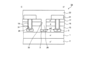
図13は、従来のSBD内蔵の炭化珪素半導体装置の構造を示す上面図である。図14は、従来のSBD内蔵の炭化珪素半導体装置の構造を示す図13のC-C’部分の断面図である。図13に示すように、SBD内蔵の炭化珪素半導体装置150は、素子構造が形成されオン状態のときに電流が流れる活性領域140と、活性領域140の周囲を囲んで耐圧を保持するエッジ領域142と、活性領域140とエッジ領域142との間のツナギ領域141と、を備える。活性領域140は図13で一点鎖線で囲まれた領域である。
Figure 13 is a top view showing the structure of a conventional silicon carbide semiconductor device with an SBD built in. Figure 14 is a cross-sectional view of part C-C' in Figure 13 showing the structure of a conventional silicon carbide semiconductor device with an SBD built in. As shown in Figure 13, a silicon
また、図14に示すように、炭化珪素からなる半導体基体(以下、炭化珪素基体とする)のおもて面(後述するp型ベース層116側の面)側に一般的なトレンチゲート構造のMOSゲートを備える。炭化珪素基体(半導体チップ)は、炭化珪素からなるn+型支持基板(以下、n+型炭化珪素基板とする)102上にn-型ドリフト層101、電流拡散領域であるn型領域115およびp型ベース層116となる各炭化珪素層を順にエピタキシャル成長させてなる。
14, a MOS gate having a general trench gate structure is provided on the front surface (the surface on the side of p-
n+型炭化珪素基板102上にn-型ドリフト層101となるn-型層をエピタキシャル成長させて、n+型炭化珪素基板102のおもて面(n-型ドリフト層101側の面)側に、p型ベース層116、n+型ソース領域117、トレンチゲート131、ゲート絶縁膜119およびゲート電極120からなるMOSゲート構造が設けられている。また、符号118、121および122は、それぞれp++型コンタクト領域、層間絶縁膜およびソース電極である。
An n - type layer to become n -
n型領域115には、トレンチゲート131の底面全体を覆うように第1p+型領域103が選択的に設けられている。また、n型領域115には、トレンチSBD132の底面全体を覆うように第1p+型領域103が選択的に設けられている。第1p+型領域103は、n-型ドリフト層101に達しない深さで設けられている。また、エッジ領域142では、第1p+型領域103の全面上に第2p+型領域104が設けられている。
A first p + -
また、トレンチSBD132は、内壁がソース電極122と接続するショットキーメタル126で覆われ、内壁に露出する半導体領域と当該ショットキーメタル126とのショットキーを形成したトレンチである。このように、図13では、ソース・ドレイン間に寄生pnダイオードと並列に寄生ショットキーダイオード(内蔵SBD)を設けている。
The trench SBD 132 is a trench whose inner wall is covered with Schottky
ソース電極122に正電圧が印加され、n+型炭化珪素基板102の裏面に設けられたドレイン電極(不図示)に負電圧が印加されたとき(MOSFETのオフ時)、p型ベース層116とn-型ドリフト層101との間のpn接合が順バイアスされる。図13において、MOSFETのオフ時に寄生pnダイオードがオンする前に寄生ショットキーダイオードがオンするように設計することで、寄生pnダイオードのバイポーラ動作を抑止し、バイポーラ動作による経年劣化を防止することができる。
When a positive voltage is applied to
また、n型領域、第1p+型領域および第2p+型領域を設け、ゲート電極に接続されるゲート電極パッドと深さ方向に対向する領域において、第1p+型領域を、トレンチゲートの幅方向に間を空けて設けることで、電流領域までPiNダイオードをバイポーラ動作させず、順方向電圧の劣化やターンオン時の損失を減少できる半導体装置が公知である(例えば、下記特許文献2参照)。
In addition, a semiconductor device is known that provides an n-type region, a first p + type region, and a second p + type region, and provides the first p + type region with a space in the width direction of the trench gate in a region that faces in the depth direction to a gate electrode pad connected to the gate electrode, thereby preventing the PiN diode from operating in bipolar mode up to the current region, and reducing deterioration of the forward voltage and loss at turn-on (see, for example,
ここで、図15は、従来のSBD内蔵の炭化珪素半導体装置の構造を示す図13のA-A’部分の断面図である。また、図16は、従来のSBD内蔵の炭化珪素半導体装置の構造を示す図13のB-B’部分の断面図である。図15および図16に示すように、ツナギ領域141では、第1p+型領域103上に第2p+型領域104が設けられている。また、p型ベース層116の表面層に、トレンチSBD132と接するp++型コンタクト領域118が設けられている。このため、ツナギ領域141において、トレンチSBD132は、周囲がp型領域(p型ベース層116、p++型コンタクト領域118、第1p+型領域103および第2p+型領域104)で囲まれている構造となっている。
Here, FIG. 15 is a cross-sectional view of the A-A' portion of FIG. 13 showing the structure of a conventional silicon carbide semiconductor device with an SBD built in. FIG. 16 is a cross-sectional view of the B-B' portion of FIG. 13 showing the structure of a conventional silicon carbide semiconductor device with an SBD built in. As shown in FIG. 15 and FIG. 16, in the
これにより、ツナギ領域141では、トレンチSBD132は寄生ショットキーダイオードとして機能せず、寄生pnダイオードのバイポーラ動作を抑止することができない。寄生pnダイオードがオンして通電した場合、寄生pnダイオードのバイポーラ動作により、ホール電流が図15および図16の経路Dのように流れ、ホール電流と電子電流による再結合によって発生したエネルギーにより、積層欠陥が発生・拡張する。
As a result, in the
このため、ツナギ領域141は、活性領域140の内部よりも、寄生pnダイオードのバイポーラ動作により経時的に特性が変化(経年劣化)し、順方向劣化やターンオン損失の増加が生じるという課題がある。
As a result, the characteristics of the
この発明は、上述した従来技術による問題点を解消するため、順方向電圧の劣化やターンオン時の損失を減少できる半導体装置を提供することを目的とする。 The purpose of this invention is to provide a semiconductor device that can reduce the degradation of forward voltage and loss at turn-on in order to solve the problems of the conventional technology described above.
上述した課題を解決し、本発明の目的を達成するため、この発明にかかる半導体装置は、次の特徴を有する。第1導電型の半導体基板のおもて面に、前記半導体基板よりも不純物濃度の低い第1導電型の第1半導体層が設けられる。前記第1半導体層の、前記半導体基板側に対して反対側に第2導電型の第2半導体層が設けられる。前記第2半導体層の内部に選択的に、前記半導体基板よりも不純物濃度の高い第1導電型の第1半導体領域が設けられる。前記第1半導体層の内部に、第2導電型の第2半導体領域が設けられる。前記第1半導体層の表面層に、前記第2半導体領域と底面が接する第2導電型の第3半導体領域が設けられる。前記第1半導体領域および前記第2半導体層を貫通して前記第1半導体層に達し、底面が前記第2半導体領域と接する第1トレンチおよび第2トレンチが設けられる。前記第1トレンチの内部にゲート絶縁膜を介してゲート電極が設けられる。前記第2トレンチの内部にショットキー電極が設けられる。オン状態のときに電流が流れる活性領域と、前記活性領域の周囲を囲んで耐圧を保持するエッジ領域との間の領域において、前記第2トレンチの側壁は、前記第2半導体領域および前記第3半導体領域と接していない。前記エッジ領域に、耐圧を向上させるための接合終端構造および第2導電型の第4半導体領域を備え、前記第2半導体領域と前記第4半導体領域との間の幅は、前記活性領域における隣り合う前記第2半導体領域間の幅以上であり、かつ、前記第2半導体領域から前記接合終端構造までの距離より狭い。
In order to solve the above-mentioned problems and achieve the object of the present invention, the semiconductor device according to the present invention has the following features. A first semiconductor layer of a first conductivity type having a lower impurity concentration than the semiconductor substrate is provided on a front surface of a semiconductor substrate of a first conductivity type. A second semiconductor layer of a second conductivity type is provided on the opposite side of the first semiconductor layer to the semiconductor substrate. A first semiconductor region of a first conductivity type having a higher impurity concentration than the semiconductor substrate is selectively provided inside the second semiconductor layer. A second semiconductor region of a second conductivity type is provided inside the first semiconductor layer. A third semiconductor region of a second conductivity type is provided in a surface layer of the first semiconductor layer, the bottom surface of which is in contact with the second semiconductor region. A first trench and a second trench are provided, which penetrate the first semiconductor region and the second semiconductor layer to reach the first semiconductor layer and have a bottom surface in contact with the second semiconductor region. A gate electrode is provided inside the first trench via a gate insulating film. A Schottky electrode is provided inside the second trench. In a region between an active region through which a current flows in an on-state and an edge region surrounding the active region to maintain a breakdown voltage, a sidewall of the second trench does not contact the second semiconductor region and the third semiconductor region. The edge region is provided with a junction termination structure for improving a breakdown voltage and a fourth semiconductor region of a second conductivity type, the width between the second semiconductor region and the fourth semiconductor region being equal to or greater than the width between adjacent second semiconductor regions in the active region and being narrower than the distance from the second semiconductor region to the junction termination structure.
上述した課題を解決し、本発明の目的を達成するため、この発明にかかる半導体装置は、次の特徴を有する。第1導電型の半導体基板のおもて面に、前記半導体基板よりも不純物濃度の低い第1導電型の第1半導体層が設けられる。前記第1半導体層の、前記半導体基板側に対して反対側に第2導電型の第2半導体層が設けられる。前記第2半導体層の内部に選択的に、前記半導体基板よりも不純物濃度の高い第1導電型の第1半導体領域が設けられる。前記第1半導体層の内部に、第2導電型の第2半導体領域が設けられる。前記第1半導体層の表面層に、前記第2半導体領域と底面が接する第2導電型の第3半導体領域が設けられる。前記第1半導体領域および前記第2半導体層を貫通して前記第1半導体層に達し、底面が前記第2半導体領域と接する第1トレンチおよび第2トレンチが設けられる。前記第1トレンチの内部にゲート絶縁膜を介してゲート電極が設けられる。前記第2トレンチの内部にショットキー電極が設けられる。オン状態のときに電流が流れる活性領域と、前記活性領域の周囲を囲んで耐圧を保持するエッジ領域との間の領域において、前記第2トレンチの側壁は、前記第2半導体領域および前記第3半導体領域と接していない。前記第2半導体層の内部に選択的に設けられ、前記第1半導体領域と接する、前記第2半導体層よりも不純物濃度の高い第2導電型の第5半導体領域を備え、前記領域において、前記第5半導体領域は、前記第2トレンチの前記エッジ領域側の側面より、前記活性領域側にある。In order to solve the above-mentioned problems and achieve the object of the present invention, the semiconductor device according to the present invention has the following features. A first semiconductor layer of a first conductivity type having a lower impurity concentration than the semiconductor substrate is provided on a front surface of a semiconductor substrate of a first conductivity type. A second semiconductor layer of a second conductivity type is provided on the opposite side of the first semiconductor layer to the semiconductor substrate. A first semiconductor region of a first conductivity type having a higher impurity concentration than the semiconductor substrate is selectively provided inside the second semiconductor layer. A second semiconductor region of a second conductivity type is provided inside the first semiconductor layer. A third semiconductor region of a second conductivity type is provided in a surface layer of the first semiconductor layer, the bottom surface of which is in contact with the second semiconductor region. A first trench and a second trench are provided, which penetrate the first semiconductor region and the second semiconductor layer to reach the first semiconductor layer and have a bottom surface in contact with the second semiconductor region. A gate electrode is provided inside the first trench via a gate insulating film. A Schottky electrode is provided inside the second trench. In a region between an active region through which a current flows in an on-state and an edge region surrounding the active region to maintain a breakdown voltage, a sidewall of the second trench is not in contact with the second semiconductor region and the third semiconductor region. A fifth semiconductor region of a second conductivity type having a higher impurity concentration than the second semiconductor layer is selectively provided inside the second semiconductor layer and in contact with the first semiconductor region, and in the region, the fifth semiconductor region is located closer to the active region than the side surface of the second trench on the edge region side.
上述した発明によれば、ツナギ領域において、トレンチSBD(第2トレンチ)の側壁は、第1、第2p+型領域(第2導電型の第2、第3半導体領域)と接していない。これにより、ツナギ領域でも、トレンチSBDを寄生ショットキーダイオードとして機能させることができる。このため、SBD内蔵の炭化珪素半導体装置のドレイン側に負バイアスがかかった際、ツナギ領域でも寄生ショットキーダイオードを動作させることによって寄生pnダイオードのバイポーラ動作を抑止することができ、順方向劣化やターンオン損失の増加を抑制できる。 According to the above-mentioned invention, in the transition region, the sidewall of the trench SBD (second trench) is not in contact with the first and second p + -type regions (second and third semiconductor regions of the second conductivity type). This allows the trench SBD to function as a parasitic Schottky diode even in the transition region. Therefore, when a negative bias is applied to the drain side of the silicon carbide semiconductor device incorporating the SBD, the parasitic Schottky diode can be operated even in the transition region to suppress the bipolar operation of the parasitic pn diode, thereby suppressing forward degradation and an increase in turn-on loss.
本発明にかかる半導体装置によれば、順方向電圧の劣化やターンオン時の損失を減少できるという効果を奏する。 The semiconductor device of the present invention has the effect of reducing the degradation of the forward voltage and the loss during turn-on.
以下に添付図面を参照して、この発明にかかる半導体装置の好適な実施の形態を詳細に説明する。本明細書および添付図面においては、nまたはpを冠記した層や領域では、それぞれ電子または正孔が多数キャリアであることを意味する。また、nやpに付す+および-は、それぞれそれが付されていない層や領域よりも高不純物濃度および低不純物濃度であることを意味する。なお、以下の実施の形態の説明および添付図面において、同様の構成には同一の符号を付し、重複する説明を省略する。また、本明細書では、ミラー指数の表記において、“-”はその直後の指数につくバーを意味しており、指数の前に“-”を付けることで負の指数をあらわしている。 Below, with reference to the attached drawings, a preferred embodiment of the semiconductor device according to the present invention will be described in detail. In this specification and the attached drawings, in layers and regions prefixed with n or p, electrons or holes, respectively, are the majority carriers. In addition, + and - appended to n or p respectively mean that the impurity concentration is higher or lower than that of layers or regions to which they are not appended. Note that in the following description of the embodiment and the attached drawings, similar configurations are given the same reference numerals, and duplicated explanations will be omitted. In addition, in this specification, in the notation of Miller indices, "-" means a bar attached to the index immediately following it, and adding "-" before an index indicates a negative index.
(実施の形態)
本発明にかかる半導体装置は、シリコンよりもバンドギャップが広い半導体(以下、ワイドバンドギャップ半導体とする)を用いて構成される。ここでは、ワイドバンドギャップ半導体として例えば炭化珪素(SiC)を用いた半導体装置(炭化珪素半導体装置)の構造を例に説明する。図1は、実施の形態にかかる炭化珪素半導体装置の構造を示す上面図である。図2は、実施の形態にかかる炭化珪素半導体装置の構造を示す図1のA-A’部分の断面図である。図3は、実施の形態にかかる炭化珪素半導体装置の構造を示す図1のB-B’部分の断面図である。図4は、実施の形態にかかる炭化珪素半導体装置の構造を示す図1のC-C’部分の断面図である。
(Embodiment)
The semiconductor device according to the present invention is configured using a semiconductor having a wider band gap than silicon (hereinafter, referred to as wide band gap semiconductor). Here, the structure of a semiconductor device (silicon carbide semiconductor device) using, for example, silicon carbide (SiC) as the wide band gap semiconductor will be described as an example. FIG. 1 is a top view showing the structure of a silicon carbide semiconductor device according to an embodiment. FIG. 2 is a cross-sectional view of an A-A' portion of FIG. 1 showing the structure of a silicon carbide semiconductor device according to an embodiment. FIG. 3 is a cross-sectional view of a B-B' portion of FIG. 1 showing the structure of a silicon carbide semiconductor device according to an embodiment. FIG. 4 is a cross-sectional view of a C-C' portion of FIG. 1 showing the structure of a silicon carbide semiconductor device according to an embodiment.
図1に示すように、SBD内蔵の炭化珪素半導体装置50は、素子構造が形成されオン状態のときに基板の厚さ方向に主電流が流れる活性領域40と、活性領域40の周囲を囲んで耐圧を保持するエッジ領域42と、活性領域40とエッジ領域42との間のツナギ領域41と、から構成される。活性領域40は図1で一点鎖線で囲まれた領域である。ツナギ領域41とは、図2に示すように、後述するトレンチゲート31の側面がp型領域で覆われMOSとして機能していない領域である。図2および図3には、1つの単位セル(素子の機能単位)のみを示し、これらに隣接する他の単位セルを図示省略する。図1~3に示す実施の形態にかかる炭化珪素半導体装置は、炭化珪素からなる半導体基体(炭化珪素基体:半導体チップ)のおもて面(後述するp型ベース層16側の面)側にMOSゲートを備えたMOSFETである。
As shown in FIG. 1, the silicon
炭化珪素基体は、炭化珪素からなるn+型支持基板(第1導電型の半導体基板)2上にn-型ドリフト層(第1導電型の第1半導体層)1およびp型ベース層(第2導電型の第2半導体層)16となる各炭化珪素層を順にエピタキシャル成長させてなる。活性領域40において、MOSゲートは、p型ベース層16と、n+型ソース領域(第1導電型の第1半導体領域)17、ゲート絶縁膜19およびゲート電極20で構成される。具体的には、n-型ドリフト層1のソース側(後述するソース電極22側)の表面層には、p型ベース層16に接するようにn型領域15が設けられていてもよい。n型領域15は、キャリアの広がり抵抗を低減させる、いわゆる電流拡散層(Current Spreading Layer:CSL)である。このn型領域15は、例えば、基体おもて面(炭化珪素基体のおもて面)に平行な方向に一様に設けられている。図2および図3では、n型領域15の記載を省略している。
The silicon carbide substrate is formed by epitaxially growing silicon carbide layers, which become an n - type drift layer (first semiconductor layer of first conductivity type) 1 and a p-type base layer (second semiconductor layer of second conductivity type) 16, in order on an n + type support substrate (semiconductor substrate of first conductivity type) 2 made of silicon carbide. In the
n型領域15(n型領域15が設けられていない場合は、n-型ドリフト層1、以下(1)と称する)の内部には、第1p+型領域(第2導電型の第2半導体領域)3が選択的に設けられている。活性領域40では、第1p+型領域3は、後述するトレンチゲート(第1トレンチ)31の底面および後述するトレンチSBD(第2トレンチ)32の底面に接するように設けられている。また、n型領域15(1)の表面層には、第2p+型領域(第2導電型の第3半導体領域)4が選択的に設けられている。第2p+型領域4は、底面が第1p+型領域3と接するように設けられている。
A first p + -type region (second semiconductor region of a second conductivity type) 3 is selectively provided inside the n-type region 15 (when the n-
n型領域15が設けられている場合、第1p+型領域3は、p型ベース層16とn型領域15との界面よりもドレイン側に深い位置から、n型領域15とn-型ドリフト層1との界面に達しない深さで設けられている。第1p+型領域3を設けることで、トレンチゲート31、トレンチSBD32の底面付近に、第1p+型領域3とn型領域15(1)との間のpn接合を形成することができる。第1p+型領域3および第2p+型領域4は、p型ベース層16よりも不純物濃度が高い。
When n-
また、p型ベース層16の内部には、n+型ソース領域17が選択的に設けられている。互いに接するようにn+型ソース領域17およびp++型コンタクト領域(第2導電型の第5半導体領域)18がそれぞれ選択的に設けられていてもよい。この場合、p++型コンタクト領域18の深さは例えばn+型ソース領域17と同じ深さでもよいし、n+型ソース領域17よりも深くてもよい。
An n +
トレンチゲート31は、基体おもて面からn+型ソース領域17およびp型ベース層16を貫通してn型領域15(1)に達する。トレンチゲート31の内部には、トレンチゲート31の側壁に沿ってゲート絶縁膜19が設けられ、ゲート絶縁膜19の内側にゲート電極20が設けられている。ゲート電極20のソース側端部は、基体おもて面から外側に突出していてもいなくてもよい。ゲート電極20は、ゲート電極パッド(不図示)に電気的に接続されている。層間絶縁膜21は、トレンチゲート31に埋め込まれたゲート電極20を覆うように基体おもて面全面に設けられている。
The
トレンチSBD32は、基体おもて面からn+型ソース領域17およびp型ベース層16を貫通してn型領域15(1)に達する。トレンチSBD32の内部には、トレンチSBD32の側壁に沿って、ソース電極22と接続するショットキーメタル26で覆われ、内壁に露出する半導体領域と当該ショットキーメタル26とのショットキー接合を形成する。また、ショットキーメタル26の内側には酸化膜、例えば、二酸化珪素(SiO2)が設けられてもよい。
Trench SBD32 reaches n-type region 15(1) from the front surface of the substrate through n + -
ここで、図1および図3に示すように、エッジ領域42では、第1p+型領域3上に、第2p+型領域4が形成されたp+型領域(第1p+領域3と第2p+型領域4をあわせた領域をp+型領域と称する。第2導電型の第4半導体領域)5が設けられている。また、図1に示すように、トレンチゲート31は、ゲートランナー(不図示)と接続するためエッジ領域42まで伸びている。図2に示すように、トレンチゲート31は、ツナギ領域41でMOSとして機能させないため、トレンチゲート31の側壁および底面は第1、第2p+型領域3、4と接している。
Here, as shown in FIG. 1 and FIG. 3, in the
一方、図1~図3に示すようにツナギ領域41において、トレンチSBD32の側壁は、第1、第2p+型領域3、4と接していない。つまり、従来のSBD内蔵の炭化珪素半導体装置において、トレンチSBD132の周囲を埋めているp+型領域5の一部を開口させることで、実施の形態のトレンチSBD32では、側壁がn型領域15(1)と接するようにしている。これにより、ツナギ領域41でも、トレンチSBD32を寄生ショットキーダイオードとして機能させるようにすることができる。このため、SBD内蔵の炭化珪素半導体装置のドレイン側に負バイアスがかかった際、ツナギ領域41でも寄生ショットキーダイオードを動作させることによって寄生pnダイオードのバイポーラ動作を抑止することができ、順方向劣化やターンオン損失の増加を抑制できる。
On the other hand, as shown in FIGS. 1 to 3, in the
図5は、実施の形態にかかる炭化珪素半導体装置の外観を示す上面図である。図5に示すように、トレンチSBD32およびトレンチゲート31は、n+型炭化珪素基板1の結晶方向が<11-20>である方向にストライプ状に設けられている。エッジ領域42には、電界を緩和または分散させることで高耐圧半導体装置全体の耐圧を向上させるため、接合終端(JTE:Junction Termination Extension)構造として、JTE領域43が設けられている。JTE領域43の外側に、チャネルストッパとして機能するn+型半導体領域(不図示)が設けられている。
5 is a top view showing the appearance of the silicon carbide semiconductor device according to the embodiment. As shown in FIG. 5, the
実施の形態では、エッジ領域42に設けられたp+型領域5とトレンチSBD32の底部に設けられた第1p+型領域3との間の幅w1(図3参照)は、活性領域40における隣り合う第1p+型領域3間の幅w2(JFET領域の幅、図14参照)以上であることが好ましい。さらに、幅w1は、第1p+型領域3からJTE領域43までの距離w3(図5参照)より狭いことが好ましい。このようにすることで、実施の形態で、従来と同程度の耐圧を維持することができる。
In the embodiment, the width w1 (see FIG. 3) between the p + -
また、従来のSBD内蔵の炭化珪素半導体装置では、ツナギ領域141において、p型ベース層116の表面層にp++型コンタクト領域118が設けられ、トレンチSBD132の側壁を取り囲んでいる(図13、図15、図16参照)。これにより、ツナギ領域141で寄生pnダイオードが動作しやすくなっていた。これに対して、実施の形態では、p++型コンタクト領域18が設けられている場合、図3に示すように、ツナギ領域41において、p++型コンタクト領域18の位置をトレンチSBD32のエッジ領域42側の側面よりも内側(活性領域40側)にしている。これにより、p++型コンタクト領域18、p型ベース層16、n-型ドリフト層1が縦に並ぶ構造を取り除き、ツナギ領域41で寄生pnダイオードが動作しにくくしている。
In the conventional silicon carbide semiconductor device with an SBD built in, the p ++
ソース電極22は、層間絶縁膜21に開口されたコンタクトホールを介してn+型ソース領域17に接するとともに、層間絶縁膜21によってゲート電極20と電気的に絶縁されている。p++型コンタクト領域18が設けられている場合、ソース電極22は、p++型コンタクト領域18とも接する。ソース電極22と層間絶縁膜21との間に、例えばソース電極22からゲート電極20側への金属原子の拡散を防止するバリアメタルを設けてもよい。ソース電極22上には、ソース電極パッド(不図示)が設けられている。炭化珪素半導体装置50の裏面(n+型ドレイン領域となるn+型炭化珪素基板1の裏面)には、ドレイン電極(不図示)が設けられている。
The source electrode 22 contacts the n +
(実施の形態にかかる半導体装置の製造方法)
次に、実施の形態にかかる半導体装置の製造方法について説明する。図6~9は、実施の形態にかかる炭化珪素半導体装置の製造途中の状態を示す断面図である。まず、n+型ドレイン領域となるn+型炭化珪素基板2を用意する。次に、n+型炭化珪素基板2のおもて面に、上述したn-型ドリフト層1をエピタキシャル成長させる。例えば、n-型ドリフト層1を形成するためのエピタキシャル成長の条件を、n-型ドリフト層1の不純物濃度が3×10¹⁵/cm3程度となるように設定してもよい。ここまでの状態が図6に記載される。
(Method of Manufacturing a Semiconductor Device According to an Embodiment)
Next, a method for manufacturing the semiconductor device according to the embodiment will be described. Figures 6 to 9 are cross-sectional views showing a state during the manufacturing of the silicon carbide semiconductor device according to the embodiment. First, an n + type
次に、n-型ドリフト層1の上に、下側n型領域15a(n型領域15を形成しない場合、n-型ドリフト層1と同程度の不純物のn型層、以下n型層と略する)をエピタキシャル成長させる。例えば、下側n型領域15aを形成するためのエピタキシャル成長の条件を、下側n型領域15aの不純物濃度が1×10¹⁷/cm3程度となるように設定してもよい。この下側n型領域15aは、n型領域15の一部である。次に、フォトリソグラフィおよびp型不純物のイオン注入により、下側n型領域15a(n型層)の表面層に、第1p+型領域3を選択的に形成する。例えば、第1p+型領域3を形成するためのイオン注入時のドーズ量を、不純物濃度が5×1018/cm3程度となるように設定してもよい。ツナギ領域41およびエッジ領域42でも、同様に第1p+型領域3を選択的に形成する。ここまでの状態が図7に記載される。
Next, on the n -
次に、下側n型領域15a(n型層)、第1p+型領域3の上に、上側n型領域15b(n型層)をエピタキシャル成長させる。例えば、上側n型領域15bを形成するためのエピタキシャル成長の条件を、下側n型領域15aの不純物濃度と同程度となるように設定してもよい。この上側n型領域15bは、n型領域15の一部であり、下側n型領域15aと上側n型領域15bを合わせて、n型領域15となる。次に、フォトリソグラフィおよびp型不純物のイオン注入により、上側n型領域15b(n型層)の表面層に、第2p+型領域4を選択的に形成する。例えば、第2p+型領域4を形成するためのイオン注入時のドーズ量を、不純物濃度が第1p+型領域3と同程度となるように設定してもよい。第1p+型領域3と第2p+型領域4とをあわせた領域を第1、第2p+型領域3、4と称する。ツナギ領域41およびエッジ領域42でも、同様に第2p+型領域4を選択的に形成する。第2p+型領域4を形成する際に、ツナギ領域41でトレンチSBD32の側壁が第2p+型領域4と接しないように形成する。ここまでの状態が図8に記載される。
Next, the upper n-
次に、上側n型領域15bおよび第2p+型領域4の上に、p型ベース層16をエピタキシャル成長させる。例えば、p型ベース層16を形成するためのエピタキシャル成長の条件を、p型ベース層16の不純物濃度が4×10¹⁷/cm3程度となるように設定してもよい。
Next, the p-
次に、フォトリソグラフィおよびn型不純物のイオン注入により、p型ベース層16の表面層にn+型ソース領域17を選択的に形成する。例えば、n+型ソース領域17を形成するためのイオン注入時のドーズ量を、不純物濃度が3×10²⁰/cm3程度となるように設定してもよい。
Next, by photolithography and ion implantation of an n-type impurity, an n + -
次に、フォトリソグラフィおよびp型不純物のイオン注入により、p型ベース層16の表面層に、n+型ソース領域17に接するようにp++型コンタクト領域18を選択的に形成してもよい。例えば、p++型コンタクト領域18を形成するためのイオン注入時のドーズ量を、不純物濃度が3×10²⁰/cm3程度となるように設定してもよい。n+型ソース領域17とp++型コンタクト領域18との形成順序を入れ替えてもよい。次に、フォトリソグラフィおよびp型不純物のイオン注入により、エッジ領域42にJTE領域43を形成する。イオン注入が全て終わった後に、活性化アニールを施す。ここまでの状態が図9に記載される。
Next, the p ++
次に、フォトリソグラフィおよびエッチングにより、n+型ソース領域17およびp型ベース層16を貫通して、n型領域15(1)に達するトレンチゲート31を形成する。トレンチゲート31の底部は、第1p+型領域3に達してもよいし、p型ベース層16と第1p+型領域3に挟まれたn型領域15(1)内に位置していてもよい。続いて、トレンチゲート31を形成するために用いたマスクを除去する。また、トレンチ形成時のマスクには酸化膜を用いる。また、トレンチエッチング後に、トレンチゲート31のダメージを除去するための等方性エッチングや、トレンチゲート31の底部およびトレンチゲート31の開口部の角を丸めるための水素アニールを施してもよい。等方性エッチングと水素アニールはどちらか一方のみを行ってもよい。また、等方性エッチングを行った後に水素アニールを行ってもよい。
Next, a
次に、フォトリソグラフィおよびエッチングにより、n+型ソース領域17およびp型ベース層16を貫通して、n型領域15(1)に達するトレンチSBD32を形成する。トレンチSBD32の底部は、第1p+型領域3に達してもよいし、p型ベース層16と第1p+型領域3に挟まれたn型領域15(1)内に位置していてもよい。続いて、トレンチSBD32を形成するために用いたマスクを除去する。この際、トレンチゲート31の端Tと、p+型領域5の距離w1は、トレンチゲート31間の間隔w2以上となり、距離w1が、第1p+型領域3とJTE領域43との幅w3より狭くなるように形成する。ここまでの状態が図10に記載される。
Next, a trench SBD32 is formed by photolithography and etching, penetrating the n +
次に、炭化珪素基体のおもて面およびトレンチゲート31の内壁に沿ってゲート絶縁膜19を形成する。次に、トレンチゲート31に埋め込むように例えばポリシリコンを堆積しエッチングすることで、トレンチゲート31の内部にゲート電極20となるポリシリコンを残す。その際、エッチバックしてポリシリコンを基体表部より内側に残すようにエッチングしてもよく、パターニングとエッチングを施すことでポリシリコンが基体表部より外側に突出していてもよい。
Next, a
次に、トレンチSBD32内壁に沿って金属膜を、例えばチタン(Ti)で形成する。次に、例えば500℃以下程度の温度の窒素(N2)雰囲気で熱処理(アニール)することで、トレンチSBD32の内壁に金属膜と半導体領域とのショットキー接合を形成する。
Next, a metal film made of, for example, titanium (Ti) is formed along the inner wall of the
次に、ゲート電極20を覆うように、炭化珪素基体のおもて面全面に層間絶縁膜21を形成する。層間絶縁膜21は、例えば、NSG(None-doped Silicate Glass:ノンドープシリケートガラス)、PSG(Phospho Silicate Glass)、BPSG(Boro Phospho Silicate Glass)、HTO(High Temperature Oxide)、あるいはそれらの組み合わせで形成される。次に、層間絶縁膜21およびゲート絶縁膜19をパターニングしてコンタクトホールを形成し、n+型ソース領域17を露出させる。p++型コンタクト領域18を形成した場合、n+型ソース領域17およびp++型コンタクト領域18を露出させる。
Next, an
次に、層間絶縁膜21を覆うようにバリアメタルを形成してパターニングし、n+型ソース領域17およびp++型コンタクト領域18を再度露出させる。次に、n+型ソース領域17に接するように、ソース電極22を形成する。ソース電極22は、バリアメタルを覆うように形成されてもよいし、コンタクトホール内にのみ残してもよい。
Next, a barrier metal is formed and patterned so as to cover the
次に、コンタクトホールを埋め込むようにソース電極パッドを形成する。ソース電極パッドを形成するために堆積した金属層の一部をゲート電極パッドとしてもよい。n+型炭化珪素基板2の裏面には、ドレイン電極のコンタクト部にスパッタ蒸着などを用いてニッケル(Ni)膜、チタン(Ti)膜などの金属膜を形成する。この金属膜は、Ni膜、Ti膜を複数組み合わせて積層してもよい。その後、金属膜がシリサイド化してオーミックコンタクトを形成するように、高速熱処理(RTA:Rapid Thermal Annealing)などのアニールを施す。その後、例えばTi膜、Ni膜、金(Au)を順に積層した積層膜などの厚い膜を電子ビーム(EB:Electron Beam)蒸着などで形成し、ドレイン電極を形成する。
Next, a source electrode pad is formed so as to fill the contact hole. A part of the metal layer deposited to form the source electrode pad may be used as a gate electrode pad. On the back surface of the n + type
上述したエピタキシャル成長およびイオン注入においては、n型不純物(n型ドーパント)として、例えば、炭化珪素に対してn型となる窒素(N)やリン(P)、ヒ素(As)、アンチモン(Sb)などを用いればよい。p型不純物(p型ドーパント)として、例えば、炭化珪素に対してp型となるホウ素(B)やアルミニウム(Al)、ガリウム(Ga)、インジウム(In)、タリウム(Tl)などを用いればよい。このようにして、図1~図4に示すMOSFETが完成する。 In the above-mentioned epitaxial growth and ion implantation, for example, nitrogen (N), phosphorus (P), arsenic (As), antimony (Sb), etc., which are n-type with respect to silicon carbide, may be used as n-type impurities (n-type dopants). For example, boron (B), aluminum (Al), gallium (Ga), indium (In), thallium (Tl), etc., which are p-type with respect to silicon carbide, may be used as p-type impurities (p-type dopants). In this way, the MOSFET shown in Figures 1 to 4 is completed.
図11は、従来のSBD内蔵の炭化珪素半導体装置のホール電流密度を示す図である。図12は、実施の形態にかかる炭化珪素半導体装置のホール電流密度を示す図である。図11および図12は、Vds=-5V、150℃の逆バイアス状態でのホール電流密度のシミュレーション結果を示す。図11および図12において、縦軸は、炭化珪素基体のおもて面からの深さを示し、単位はμmである。また、横軸は、活性領域40のトレンチSBD32の端部(図1のT)からの長さを示し、単位はμmである。
Figure 11 is a diagram showing the hole current density of a conventional silicon carbide semiconductor device with an embedded SBD. Figure 12 is a diagram showing the hole current density of a silicon carbide semiconductor device according to an embodiment. Figures 11 and 12 show simulation results of the hole current density in a reverse bias state at Vds = -5V and 150°C. In Figures 11 and 12, the vertical axis indicates the depth from the front surface of the silicon carbide substrate in μm. The horizontal axis indicates the length from the end of the
図11および図12に示すように、実施の形態にかかる炭化珪素半導体装置では、ツナギ領域41のホール電流密度が、従来のSBD内蔵の炭化珪素半導体装置より大幅に低くなっている。このため、実施の形態にかかる炭化珪素半導体装置では、n+型炭化珪素基板1に入るホールが減少して、積層欠陥の発生・拡張を抑止できる。
11 and 12 , in the silicon carbide semiconductor device according to the embodiment, the hole current density in the
以上、説明したように、実施の形態によれば、ツナギ領域41において、トレンチSBDの側壁は、第1、第2p+型領域と接していない。これにより、ツナギ領域41でも、トレンチSBDを寄生ショットキーダイオードとして機能させることができる。このため、SBD内蔵の炭化珪素半導体装置のドレイン側に負バイアスがかかった際、ツナギ領域41でも寄生ショットキーダイオードを動作させることによって寄生pnダイオードのバイポーラ動作を抑止することができ、順方向劣化やターンオン損失の増加を抑制できる。
As described above, according to the embodiment, in the
以上において本発明は本発明の趣旨を逸脱しない範囲で種々変更可能であり、上述した各実施の形態において、例えば各部の寸法や不純物濃度等は要求される仕様等に応じて種々設定される。また、上述した各実施の形態では、MOSFETを例に説明しているが、これに限らず、所定のゲート閾値電圧に基づいてゲート駆動制御されることで電流を導通および遮断する種々な炭化珪素半導体装置にも広く適用可能である。ゲート駆動制御される炭化珪素半導体装置として、例えばIGBT(Insulated Gate Bipolar Transistor:絶縁ゲート型バイポーラトランジスタ)などが挙げられる。また、上述した各実施の形態では、ワイドバンドギャップ半導体として炭化珪素を用いた場合を例に説明しているが、炭化珪素以外の例えば窒化ガリウム(GaN)などのワイドバンドギャップ半導体にも適用可能である。また、各実施の形態では第1導電型をn型とし、第2導電型をp型としたが、本発明は第1導電型をp型とし、第2導電型をn型としても同様に成り立つ。 The present invention can be modified in various ways without departing from the spirit of the present invention. In each of the above-mentioned embodiments, for example, the dimensions and impurity concentration of each part are set in various ways according to the required specifications. In addition, in each of the above-mentioned embodiments, a MOSFET is used as an example, but the present invention can be widely applied to various silicon carbide semiconductor devices that conduct and cut off current by being gate-driven and controlled based on a predetermined gate threshold voltage. Examples of silicon carbide semiconductor devices that are gate-driven and controlled include IGBTs (Insulated Gate Bipolar Transistors). In each of the above-mentioned embodiments, silicon carbide is used as a wide band gap semiconductor, but the present invention can also be applied to wide band gap semiconductors other than silicon carbide, such as gallium nitride (GaN). In each of the above-mentioned embodiments, the first conductivity type is n-type and the second conductivity type is p-type, but the present invention is similarly valid even if the first conductivity type is p-type and the second conductivity type is n-type.
以上のように、本発明にかかる半導体装置は、電力変換装置や種々の産業用機械などの電源装置などに使用されるパワー半導体装置に有用であり、特にトレンチゲート構造の炭化珪素半導体装置に適している。 As described above, the semiconductor device according to the present invention is useful for power semiconductor devices used in power conversion devices and power supply devices for various industrial machines, and is particularly suitable for silicon carbide semiconductor devices with a trench gate structure.
1、101 n-型ドリフト層
2、102 n+型炭化珪素基板
3、103 第1p+型領域
4、104 第2p+型領域
5 p+型領域
15、115 n型領域
15a 下側n型領域
15b 上側n型領域
16、116 p型ベース層
17、117 n+型ソース領域
18、118 p++型コンタクト領域
19、119 ゲート絶縁膜
20、120 ゲート電極
21、121 層間絶縁膜
22、122 ソース電極
26、126 ショットキーメタル
31、131 トレンチゲート
32、132 トレンチSBD
40、140 活性領域
41、141 ツナギ領域
42、142 エッジ領域
43 JTE領域
50、150 SBD内蔵の炭化珪素半導体装置
1, 101 n -
40, 140
Claims (2)
前記半導体基板のおもて面に設けられた、前記半導体基板よりも不純物濃度の低い第1導電型の第1半導体層と、
前記第1半導体層の、前記半導体基板側に対して反対側に設けられた第2導電型の第2半導体層と、
前記第2半導体層の内部に選択的に設けられた、前記半導体基板よりも不純物濃度の高い第1導電型の第1半導体領域と、
前記第1半導体層の内部に設けられた、第2導電型の第2半導体領域と、
前記第1半導体層の表面層に設けられ、前記第2半導体領域と底面が接する第2導電型の第3半導体領域と、
前記第1半導体領域および前記第2半導体層を貫通して前記第1半導体層に達し、底面が前記第2半導体領域と接する第1トレンチおよび第2トレンチと、
前記第1トレンチの内部にゲート絶縁膜を介して設けられたゲート電極と、
前記第2トレンチの内部に設けられたショットキー電極と、
を備え、
オン状態のときに電流が流れる活性領域と、前記活性領域の周囲を囲んで耐圧を保持するエッジ領域との間の領域において、前記第2トレンチの側壁は、前記第2半導体領域および前記第3半導体領域と接していなく、
前記エッジ領域に、耐圧を向上させるための接合終端構造および第2導電型の第4半導体領域を備え、
前記第2半導体領域と前記第4半導体領域との間の幅は、前記活性領域における隣り合う前記第2半導体領域間の幅以上であり、かつ、前記第2半導体領域から前記接合終端構造までの距離より狭いことを特徴とする半導体装置。 a semiconductor substrate of a first conductivity type;
a first semiconductor layer of a first conductivity type provided on a front surface of the semiconductor substrate and having a lower impurity concentration than the semiconductor substrate;
a second semiconductor layer of a second conductivity type provided on the opposite side of the first semiconductor layer with respect to the semiconductor substrate;
a first semiconductor region of a first conductivity type selectively provided within the second semiconductor layer and having a higher impurity concentration than the semiconductor substrate;
a second semiconductor region of a second conductivity type provided within the first semiconductor layer;
a third semiconductor region of a second conductivity type provided in a surface layer of the first semiconductor layer and having a bottom surface in contact with the second semiconductor region;
a first trench and a second trench that penetrate the first semiconductor region and the second semiconductor layer to reach the first semiconductor layer and have a bottom surface in contact with the second semiconductor region;
a gate electrode provided inside the first trench via a gate insulating film;
a Schottky electrode provided inside the second trench;
Equipped with
In a region between an active region through which a current flows in an on-state and an edge region surrounding the active region and maintaining a withstand voltage, a sidewall of the second trench is not in contact with the second semiconductor region and the third semiconductor region;
a junction termination structure for improving a breakdown voltage and a fourth semiconductor region of a second conductivity type are provided in the edge region;
A semiconductor device, characterized in that the width between the second semiconductor region and the fourth semiconductor region is greater than or equal to the width between adjacent second semiconductor regions in the active region, and is narrower than the distance from the second semiconductor region to the junction termination structure .
前記半導体基板のおもて面に設けられた、前記半導体基板よりも不純物濃度の低い第1導電型の第1半導体層と、a first semiconductor layer of a first conductivity type provided on a front surface of the semiconductor substrate and having a lower impurity concentration than the semiconductor substrate;
前記第1半導体層の、前記半導体基板側に対して反対側に設けられた第2導電型の第2半導体層と、a second semiconductor layer of a second conductivity type provided on the opposite side of the first semiconductor layer with respect to the semiconductor substrate;
前記第2半導体層の内部に選択的に設けられた、前記半導体基板よりも不純物濃度の高い第1導電型の第1半導体領域と、a first semiconductor region of a first conductivity type selectively provided within the second semiconductor layer and having a higher impurity concentration than the semiconductor substrate;
前記第1半導体層の内部に設けられた、第2導電型の第2半導体領域と、a second semiconductor region of a second conductivity type provided within the first semiconductor layer;
前記第1半導体層の表面層に設けられ、前記第2半導体領域と底面が接する第2導電型の第3半導体領域と、a third semiconductor region of a second conductivity type provided in a surface layer of the first semiconductor layer and having a bottom surface in contact with the second semiconductor region;
前記第1半導体領域および前記第2半導体層を貫通して前記第1半導体層に達し、底面が前記第2半導体領域と接する第1トレンチおよび第2トレンチと、a first trench and a second trench that penetrate the first semiconductor region and the second semiconductor layer to reach the first semiconductor layer and have a bottom surface in contact with the second semiconductor region;
前記第1トレンチの内部にゲート絶縁膜を介して設けられたゲート電極と、a gate electrode provided inside the first trench via a gate insulating film;
前記第2トレンチの内部に設けられたショットキー電極と、a Schottky electrode provided inside the second trench;
を備え、Equipped with
オン状態のときに電流が流れる活性領域と、前記活性領域の周囲を囲んで耐圧を保持するエッジ領域との間の領域において、前記第2トレンチの側壁は、前記第2半導体領域および前記第3半導体領域と接していなく、In a region between an active region through which a current flows in an on-state and an edge region surrounding the active region and maintaining a withstand voltage, a sidewall of the second trench is not in contact with the second semiconductor region and the third semiconductor region;
前記第2半導体層の内部に選択的に設けられ、前記第1半導体領域と接する、前記第2半導体層よりも不純物濃度の高い第2導電型の第5半導体領域を備え、a fifth semiconductor region of a second conductivity type selectively provided within the second semiconductor layer and in contact with the first semiconductor region, the fifth semiconductor region having an impurity concentration higher than that of the second semiconductor layer;
前記領域において、前記第5半導体領域は、前記第2トレンチの前記エッジ領域側の側面より、前記活性領域側にあることを特徴とする半導体装置。In the region, the fifth semiconductor region is located closer to the active region than the side surface of the second trench on the edge region side.
Priority Applications (1)
| Application Number | Priority Date | Filing Date | Title |
|---|---|---|---|
| US17/558,004 US12119399B2 (en) | 2020-06-19 | 2021-12-21 | Semiconductor device including vertical MOSFET and Schottky barrier diode |
Applications Claiming Priority (2)
| Application Number | Priority Date | Filing Date | Title |
|---|---|---|---|
| JP2020106596 | 2020-06-19 | ||
| JP2020106596 | 2020-06-19 |
Publications (2)
| Publication Number | Publication Date |
|---|---|
| JP2022002290A JP2022002290A (en) | 2022-01-06 |
| JP7640930B2 true JP7640930B2 (en) | 2025-03-06 |
Family
ID=79244449
Family Applications (1)
| Application Number | Title | Priority Date | Filing Date |
|---|---|---|---|
| JP2020212973A Active JP7640930B2 (en) | 2020-06-19 | 2020-12-22 | Semiconductor Device |
Country Status (2)
| Country | Link |
|---|---|
| US (1) | US12119399B2 (en) |
| JP (1) | JP7640930B2 (en) |
Families Citing this family (2)
| Publication number | Priority date | Publication date | Assignee | Title |
|---|---|---|---|---|
| JP2023110952A (en) * | 2022-01-31 | 2023-08-10 | 国立研究開発法人産業技術総合研究所 | semiconductor equipment |
| JP2024011224A (en) * | 2022-07-14 | 2024-01-25 | 富士電機株式会社 | silicon carbide semiconductor device |
Citations (3)
| Publication number | Priority date | Publication date | Assignee | Title |
|---|---|---|---|---|
| JP2015076592A (en) | 2013-10-11 | 2015-04-20 | 住友電気工業株式会社 | Silicon carbide semiconductor device and manufacturing method of the same |
| JP2018182234A (en) | 2017-04-20 | 2018-11-15 | 富士電機株式会社 | Silicon carbide semiconductor device and method of manufacturing silicon carbide semiconductor device |
| JP2019216223A (en) | 2018-06-14 | 2019-12-19 | 富士電機株式会社 | Semiconductor device |
Family Cites Families (8)
| Publication number | Priority date | Publication date | Assignee | Title |
|---|---|---|---|---|
| JPH08204179A (en) | 1995-01-26 | 1996-08-09 | Fuji Electric Co Ltd | Silicon Carbide Trench MOSFET |
| US20120306009A1 (en) * | 2011-06-03 | 2012-12-06 | Suku Kim | Integration of superjunction mosfet and diode |
| JP6740759B2 (en) * | 2016-07-05 | 2020-08-19 | 株式会社デンソー | Silicon carbide semiconductor device and manufacturing method thereof |
| JP6696328B2 (en) * | 2016-07-05 | 2020-05-20 | 株式会社デンソー | Silicon carbide semiconductor device and manufacturing method thereof |
| JP6914624B2 (en) * | 2016-07-05 | 2021-08-04 | 株式会社デンソー | Silicon carbide semiconductor device and its manufacturing method |
| JP6988140B2 (en) * | 2017-04-12 | 2022-01-05 | 富士電機株式会社 | Silicon Carbide Semiconductor Device and Method for Manufacturing Silicon Carbide Semiconductor Device |
| JP7029711B2 (en) * | 2017-11-29 | 2022-03-04 | 国立研究開発法人産業技術総合研究所 | Semiconductor device |
| JP7243094B2 (en) * | 2018-09-11 | 2023-03-22 | 富士電機株式会社 | semiconductor equipment |
-
2020
- 2020-12-22 JP JP2020212973A patent/JP7640930B2/en active Active
-
2021
- 2021-12-21 US US17/558,004 patent/US12119399B2/en active Active
Patent Citations (3)
| Publication number | Priority date | Publication date | Assignee | Title |
|---|---|---|---|---|
| JP2015076592A (en) | 2013-10-11 | 2015-04-20 | 住友電気工業株式会社 | Silicon carbide semiconductor device and manufacturing method of the same |
| JP2018182234A (en) | 2017-04-20 | 2018-11-15 | 富士電機株式会社 | Silicon carbide semiconductor device and method of manufacturing silicon carbide semiconductor device |
| JP2019216223A (en) | 2018-06-14 | 2019-12-19 | 富士電機株式会社 | Semiconductor device |
Also Published As
| Publication number | Publication date |
|---|---|
| US20220199823A1 (en) | 2022-06-23 |
| US12119399B2 (en) | 2024-10-15 |
| JP2022002290A (en) | 2022-01-06 |
Similar Documents
| Publication | Publication Date | Title |
|---|---|---|
| JP7509254B2 (en) | Semiconductor Device | |
| JP7563526B2 (en) | Method for manufacturing an insulated gate semiconductor device | |
| US10276666B2 (en) | Semiconductor device | |
| JP6930197B2 (en) | Semiconductor devices and manufacturing methods for semiconductor devices | |
| JP2019054064A (en) | Semiconductor device | |
| US10439060B2 (en) | Semiconductor device and method of manufacturing semiconductor device | |
| JP7459975B2 (en) | Insulated gate semiconductor device | |
| JP7683677B2 (en) | Semiconductor Device | |
| JP7029711B2 (en) | Semiconductor device | |
| JP7768317B2 (en) | Semiconductor Devices | |
| JP7379880B2 (en) | semiconductor equipment | |
| JP7625903B2 (en) | Insulated gate semiconductor device | |
| JP7172216B2 (en) | Semiconductor devices and semiconductor circuit devices | |
| JP7290973B2 (en) | semiconductor equipment | |
| JP7640930B2 (en) | Semiconductor Device | |
| JP7501000B2 (en) | Semiconductor Device | |
| JP7476502B2 (en) | Semiconductor Device | |
| JP7661711B2 (en) | Silicon carbide semiconductor device | |
| JP7643179B2 (en) | Silicon carbide semiconductor device | |
| US12426330B2 (en) | Semiconductor device | |
| JP7731660B2 (en) | Semiconductor device and method for manufacturing the same | |
| JP7585661B2 (en) | Semiconductor Device |
Legal Events
| Date | Code | Title | Description |
|---|---|---|---|
| A711 | Notification of change in applicant |
Free format text: JAPANESE INTERMEDIATE CODE: A711 Effective date: 20211210 |
|
| A521 | Request for written amendment filed |
Free format text: JAPANESE INTERMEDIATE CODE: A821 Effective date: 20211213 |
|
| A621 | Written request for application examination |
Free format text: JAPANESE INTERMEDIATE CODE: A621 Effective date: 20231117 |
|
| A977 | Report on retrieval |
Free format text: JAPANESE INTERMEDIATE CODE: A971007 Effective date: 20240816 |
|
| A131 | Notification of reasons for refusal |
Free format text: JAPANESE INTERMEDIATE CODE: A131 Effective date: 20240820 |
|
| A521 | Request for written amendment filed |
Free format text: JAPANESE INTERMEDIATE CODE: A523 Effective date: 20241018 |
|
| A521 | Request for written amendment filed |
Free format text: JAPANESE INTERMEDIATE CODE: A821 Effective date: 20241018 |
|
| TRDD | Decision of grant or rejection written | ||
| A01 | Written decision to grant a patent or to grant a registration (utility model) |
Free format text: JAPANESE INTERMEDIATE CODE: A01 Effective date: 20250114 |
|
| A61 | First payment of annual fees (during grant procedure) |
Free format text: JAPANESE INTERMEDIATE CODE: A61 Effective date: 20250204 |
|
| R150 | Certificate of patent or registration of utility model |
Ref document number: 7640930 Country of ref document: JP Free format text: JAPANESE INTERMEDIATE CODE: R150 |