JP7607071B2 - Magnetic sensor device, inverter device, battery device, electric motor and vehicle - Google Patents
Magnetic sensor device, inverter device, battery device, electric motor and vehicle Download PDFInfo
- Publication number
- JP7607071B2 JP7607071B2 JP2023070123A JP2023070123A JP7607071B2 JP 7607071 B2 JP7607071 B2 JP 7607071B2 JP 2023070123 A JP2023070123 A JP 2023070123A JP 2023070123 A JP2023070123 A JP 2023070123A JP 7607071 B2 JP7607071 B2 JP 7607071B2
- Authority
- JP
- Japan
- Prior art keywords
- magnetic field
- value
- detection signal
- magnetic
- target
- Prior art date
- Legal status (The legal status is an assumption and is not a legal conclusion. Google has not performed a legal analysis and makes no representation as to the accuracy of the status listed.)
- Active
Links
- 230000005291 magnetic effect Effects 0.000 title claims description 375
- 238000001514 detection method Methods 0.000 claims description 156
- 230000008859 change Effects 0.000 claims description 27
- 239000004020 conductor Substances 0.000 claims description 16
- 230000000694 effects Effects 0.000 claims description 15
- 230000004907 flux Effects 0.000 claims description 8
- 230000005415 magnetization Effects 0.000 description 29
- 238000010586 diagram Methods 0.000 description 14
- 230000004044 response Effects 0.000 description 8
- 230000005290 antiferromagnetic effect Effects 0.000 description 4
- 230000007423 decrease Effects 0.000 description 4
- 238000000034 method Methods 0.000 description 4
- 239000000758 substrate Substances 0.000 description 4
- 230000005294 ferromagnetic effect Effects 0.000 description 3
- 238000005259 measurement Methods 0.000 description 3
- 230000009471 action Effects 0.000 description 2
- 238000013459 approach Methods 0.000 description 2
- 238000012937 correction Methods 0.000 description 2
- 230000035945 sensitivity Effects 0.000 description 2
- 230000005856 abnormality Effects 0.000 description 1
- 239000002885 antiferromagnetic material Substances 0.000 description 1
- 230000004888 barrier function Effects 0.000 description 1
- 230000008878 coupling Effects 0.000 description 1
- 238000010168 coupling process Methods 0.000 description 1
- 238000005859 coupling reaction Methods 0.000 description 1
- 239000000696 magnetic material Substances 0.000 description 1
- 238000004519 manufacturing process Methods 0.000 description 1
- 238000012986 modification Methods 0.000 description 1
- 230000004048 modification Effects 0.000 description 1
- 238000012544 monitoring process Methods 0.000 description 1
Images


Classifications
-
- G—PHYSICS
- G01—MEASURING; TESTING
- G01R—MEASURING ELECTRIC VARIABLES; MEASURING MAGNETIC VARIABLES
- G01R15/00—Details of measuring arrangements of the types provided for in groups G01R17/00 - G01R29/00, G01R33/00 - G01R33/26 or G01R35/00
- G01R15/14—Adaptations providing voltage or current isolation, e.g. for high-voltage or high-current networks
- G01R15/20—Adaptations providing voltage or current isolation, e.g. for high-voltage or high-current networks using galvano-magnetic devices, e.g. Hall-effect devices, i.e. measuring a magnetic field via the interaction between a current and a magnetic field, e.g. magneto resistive or Hall effect devices
- G01R15/207—Constructional details independent of the type of device used
-
- G—PHYSICS
- G01—MEASURING; TESTING
- G01R—MEASURING ELECTRIC VARIABLES; MEASURING MAGNETIC VARIABLES
- G01R15/00—Details of measuring arrangements of the types provided for in groups G01R17/00 - G01R29/00, G01R33/00 - G01R33/26 or G01R35/00
- G01R15/14—Adaptations providing voltage or current isolation, e.g. for high-voltage or high-current networks
- G01R15/20—Adaptations providing voltage or current isolation, e.g. for high-voltage or high-current networks using galvano-magnetic devices, e.g. Hall-effect devices, i.e. measuring a magnetic field via the interaction between a current and a magnetic field, e.g. magneto resistive or Hall effect devices
- G01R15/205—Adaptations providing voltage or current isolation, e.g. for high-voltage or high-current networks using galvano-magnetic devices, e.g. Hall-effect devices, i.e. measuring a magnetic field via the interaction between a current and a magnetic field, e.g. magneto resistive or Hall effect devices using magneto-resistance devices, e.g. field plates
-
- G—PHYSICS
- G01—MEASURING; TESTING
- G01R—MEASURING ELECTRIC VARIABLES; MEASURING MAGNETIC VARIABLES
- G01R31/00—Arrangements for testing electric properties; Arrangements for locating electric faults; Arrangements for electrical testing characterised by what is being tested not provided for elsewhere
- G01R31/36—Arrangements for testing, measuring or monitoring the electrical condition of accumulators or electric batteries, e.g. capacity or state of charge [SoC]
- G01R31/364—Battery terminal connectors with integrated measuring arrangements
-
- G—PHYSICS
- G01—MEASURING; TESTING
- G01R—MEASURING ELECTRIC VARIABLES; MEASURING MAGNETIC VARIABLES
- G01R33/00—Arrangements or instruments for measuring magnetic variables
- G01R33/0011—Arrangements or instruments for measuring magnetic variables comprising means, e.g. flux concentrators, flux guides, for guiding or concentrating the magnetic flux, e.g. to the magnetic sensor
-
- G—PHYSICS
- G01—MEASURING; TESTING
- G01R—MEASURING ELECTRIC VARIABLES; MEASURING MAGNETIC VARIABLES
- G01R33/00—Arrangements or instruments for measuring magnetic variables
- G01R33/0017—Means for compensating offset magnetic fields or the magnetic flux to be measured; Means for generating calibration magnetic fields
-
- G—PHYSICS
- G01—MEASURING; TESTING
- G01R—MEASURING ELECTRIC VARIABLES; MEASURING MAGNETIC VARIABLES
- G01R33/00—Arrangements or instruments for measuring magnetic variables
- G01R33/0023—Electronic aspects, e.g. circuits for stimulation, evaluation, control; Treating the measured signals; calibration
- G01R33/0041—Electronic aspects, e.g. circuits for stimulation, evaluation, control; Treating the measured signals; calibration using feed-back or modulation techniques
-
- G—PHYSICS
- G01—MEASURING; TESTING
- G01R—MEASURING ELECTRIC VARIABLES; MEASURING MAGNETIC VARIABLES
- G01R33/00—Arrangements or instruments for measuring magnetic variables
- G01R33/007—Environmental aspects, e.g. temperature variations, radiation, stray fields
- G01R33/0076—Protection, e.g. with housings against stray fields
-
- G—PHYSICS
- G01—MEASURING; TESTING
- G01R—MEASURING ELECTRIC VARIABLES; MEASURING MAGNETIC VARIABLES
- G01R33/00—Arrangements or instruments for measuring magnetic variables
- G01R33/02—Measuring direction or magnitude of magnetic fields or magnetic flux
- G01R33/06—Measuring direction or magnitude of magnetic fields or magnetic flux using galvano-magnetic devices
- G01R33/07—Hall effect devices
-
- G—PHYSICS
- G01—MEASURING; TESTING
- G01R—MEASURING ELECTRIC VARIABLES; MEASURING MAGNETIC VARIABLES
- G01R33/00—Arrangements or instruments for measuring magnetic variables
- G01R33/02—Measuring direction or magnitude of magnetic fields or magnetic flux
- G01R33/06—Measuring direction or magnitude of magnetic fields or magnetic flux using galvano-magnetic devices
- G01R33/09—Magnetoresistive devices
- G01R33/093—Magnetoresistive devices using multilayer structures, e.g. giant magnetoresistance sensors
-
- G—PHYSICS
- G01—MEASURING; TESTING
- G01R—MEASURING ELECTRIC VARIABLES; MEASURING MAGNETIC VARIABLES
- G01R33/00—Arrangements or instruments for measuring magnetic variables
- G01R33/02—Measuring direction or magnitude of magnetic fields or magnetic flux
- G01R33/06—Measuring direction or magnitude of magnetic fields or magnetic flux using galvano-magnetic devices
- G01R33/09—Magnetoresistive devices
- G01R33/098—Magnetoresistive devices comprising tunnel junctions, e.g. tunnel magnetoresistance sensors
Landscapes
- Physics & Mathematics (AREA)
- General Physics & Mathematics (AREA)
- Condensed Matter Physics & Semiconductors (AREA)
- Health & Medical Sciences (AREA)
- Engineering & Computer Science (AREA)
- Environmental & Geological Engineering (AREA)
- Toxicology (AREA)
- Measuring Instrument Details And Bridges, And Automatic Balancing Devices (AREA)
- Measuring Magnetic Variables (AREA)
- Hall/Mr Elements (AREA)
- Measurement Of Current Or Voltage (AREA)
Description
本発明は、磁気センサ装置、磁気センサ装置を備えたインバータ装置、磁気センサ装置を備えたバッテリ装置、インバータ装置が接続された電動モータ、バッテリ装置が接続された電動モータ、およびインバータ装置またはバッテリ装置と電動モータとを備えた車両に関する。 The present invention relates to a magnetic sensor device, an inverter device equipped with a magnetic sensor device, a battery device equipped with a magnetic sensor device, an electric motor connected to an inverter device, an electric motor connected to a battery device, and a vehicle equipped with an inverter device or a battery device and an electric motor.
電気自動車、ハイブリッド自動車およびプラグインハイブリッド自動車等の電動モータを使用した車両には、電動モータを制御するインバータ装置や、インバータ装置を介して電動モータに高電圧の電力を供給するバッテリ装置が搭載されている。インバータ装置やバッテリ装置では、回路を流れる電流を測定するために、電流センサが用いられている。インバータ装置やバッテリ装置等の大電流が流れる回路で用いられる電流センサとしては、非接触の磁気式の電流センサが知られている。 Vehicles that use electric motors, such as electric vehicles, hybrid vehicles, and plug-in hybrid vehicles, are equipped with an inverter device that controls the electric motor, and a battery device that supplies high-voltage power to the electric motor via the inverter device. Inverter devices and battery devices use current sensors to measure the current flowing through the circuit. Non-contact magnetic current sensors are known as current sensors used in circuits through which large currents flow, such as inverter devices and battery devices.
磁気式の電流センサとしては、磁気比例方式の電流センサと、磁気平衡方式の電流センサが知られている。磁気比例方式の電流センサでは、磁気検出素子を含む磁気センサが、導体を流れる検出対象電流によって発生する対象磁界を検出して、対象磁界の強度と対応関係を有する検出値を生成する。磁気センサの検出値は、検出対象電流の値と比例関係にある。従って、磁気センサの検出値は、検出対象電流の検出値に相当する。 Known magnetic current sensors include magnetic proportional current sensors and magnetic balance current sensors. In a magnetic proportional current sensor, a magnetic sensor including a magnetic detection element detects a target magnetic field generated by a target current flowing through a conductor, and generates a detection value that corresponds to the strength of the target magnetic field. The detection value of the magnetic sensor is proportional to the value of the target current. Therefore, the detection value of the magnetic sensor corresponds to the detection value of the target current.
磁気平衡方式の電流センサは、導体を流れる検出対象電流によって発生する対象磁界をキャンセルするためのキャンセル磁界を発生するフィードバックコイルと、対象磁界とキャンセル磁界との残差の磁界(以下、残差磁界と言う。)を検出して残差磁界の検出値を出力する磁気センサと、磁気センサから出力される検出値に応じて、フィードバックコイルに流すフィードバック電流を制御する制御回路と、フィードバック電流の電流路に挿入された抵抗器を含む検出回路とを備えている。抵抗器の両端の電位差は、フィードバック電流の検出値に相当する。フィードバック電流の検出値は、検出対象電流の値と比例関係にある。従って、フィードバック電流の検出値は、検出対象電流の検出値に相当する。この磁気平衡方式の電流センサは、残差磁界の強度がゼロに近づくように動作する。 A magnetic balance type current sensor includes a feedback coil that generates a cancellation magnetic field to cancel the target magnetic field generated by the target current flowing through a conductor, a magnetic sensor that detects the residual magnetic field between the target magnetic field and the cancellation magnetic field (hereinafter referred to as the residual magnetic field) and outputs the detection value of the residual magnetic field, a control circuit that controls the feedback current flowing through the feedback coil according to the detection value output from the magnetic sensor, and a detection circuit that includes a resistor inserted in the current path of the feedback current. The potential difference across the resistor corresponds to the detection value of the feedback current. The detection value of the feedback current is proportional to the value of the target current. Therefore, the detection value of the feedback current corresponds to the detection value of the target current. This magnetic balance type current sensor operates so that the strength of the residual magnetic field approaches zero.
インバータ装置やバッテリ装置では特に、測定範囲の広い電流センサが求められる。特許文献1ないし3には、磁気比例方式と磁気平衡方式とを組み合わせて、測定範囲を広くした電流センサが開示されている。
Current sensors with a wide measurement range are particularly required for inverter devices and battery devices.
ところで、バッテリ装置においては、バッテリ容量の有効活用のために、測定した電流値の積算値からバッテリの残量を正確に推定したいという要求がある。バッテリの残量を正確に推定するためには、特に、検出対象電流の値が小さくなる領域、すなわち対象磁界の強度が小さくなる領域において、精度よく検出対象電流を測定することが求められる。磁気平衡方式は、原理的に、磁気検出素子のオフセットと、磁気検出素子の非線形性が解消される。そのため、対象磁界の強度が小さくなる領域においては、磁気平衡方式によって検出対象電流を測定することが望ましい。 In battery devices, there is a demand for accurately estimating the remaining battery charge from the integrated value of the measured current value in order to effectively utilize the battery capacity. In order to accurately estimate the remaining battery charge, it is necessary to measure the current to be detected with high accuracy, particularly in the region where the value of the current to be detected is small, i.e., the region where the intensity of the target magnetic field is small. In principle, the magnetic balance method eliminates the offset of the magnetic detection element and the nonlinearity of the magnetic detection element. Therefore, in the region where the intensity of the target magnetic field is small, it is desirable to measure the current to be detected using the magnetic balance method.
特許文献2には、被検出電流が小さいときには、磁気平衡検出式による電流検出を選択することと、被検出電流が小さいときには、センサ出力に相当する集積チップからの出力信号(ホール電圧)の値が、被検出電流の値に比例することが記載されている。特許文献3には、磁気平衡式の電流センサの特性と一致する出力電圧を、相対的に電流入力範囲が狭い場合の出力として利用することと、低電流領域では、磁気平衡式の電流センサの特性と一致する出力電圧の値と、磁気比例式の電流センサにおける出力電圧の値が、いずれも、被測定電流の値に比例することが記載されている。
車両において使用される電流センサには、瞬間的に強度が変化するノイズ磁界が印加される場合がある。以下、このノイズ磁界を、パルス状のノイズ磁界と言う。パルス状のノイズ磁界の検出は、異常検出等の観点から有益である。しかし、従来は、電流センサにおいてパルス状のノイズ磁界を検出することは考慮されていなかった。また、磁気平衡方式の電流センサは、原理上、磁気比例方式の電流センサに比べて応答速度が遅くなる。すなわち、磁気平衡方式の電流センサでは、パルス状のノイズ磁界が印加されても、フィードバック電流の検出値はほとんど変化しないため、パルス状のノイズ磁界を検出することが難しい。 Current sensors used in vehicles may be subjected to a noise magnetic field whose strength changes instantaneously. Hereinafter, this noise magnetic field will be referred to as a pulsed noise magnetic field. Detecting a pulsed noise magnetic field is useful from the standpoint of detecting abnormalities, etc. However, in the past, detecting a pulsed noise magnetic field in a current sensor was not considered. Also, in principle, a magnetic balance type current sensor has a slower response speed than a magnetic proportional type current sensor. That is, with a magnetic balance type current sensor, even if a pulsed noise magnetic field is applied, the detected value of the feedback current hardly changes, making it difficult to detect a pulsed noise magnetic field.
上記の問題は、電流センサに限らず、対象磁界を検出する磁気センサ装置全般に当てはまる。 The above problem is not limited to current sensors, but applies to all magnetic sensor devices that detect target magnetic fields.
本発明はかかる問題点に鑑みてなされたもので、その目的は、パルス状のノイズ磁界を検出することが可能な磁気センサ装置、インバータ装置、バッテリ装置、電動モータおよび車両を提供することにある。 The present invention was made in consideration of these problems, and its purpose is to provide a magnetic sensor device, inverter device, battery device, electric motor, and vehicle that are capable of detecting pulsed noise magnetic fields.
本発明の磁気センサ装置は、印加磁界を検出する磁気検出素子を含み、印加磁界の強度と対応関係を有する第1の検出信号を生成する第1の検出回路と、フィードバック電流が流されることによって、検出対象の磁界である対象磁界の少なくとも一部を相殺するためのキャンセル磁界を発生するフィードバックコイルと、フィードバック電流の値と対応関係を有する第2の検出信号を生成する第2の検出回路とを備えている。 The magnetic sensor device of the present invention includes a magnetic detection element that detects an applied magnetic field, a first detection circuit that generates a first detection signal that corresponds to the strength of the applied magnetic field, a feedback coil that generates a cancellation magnetic field for canceling at least a portion of the target magnetic field, which is the magnetic field to be detected, by passing a feedback current through it, and a second detection circuit that generates a second detection signal that corresponds to the value of the feedback current.
対象磁界の強度が第1の値よりも大きく第2の値未満の第1の場合には第1の検出信号が一定値になるようにフィードバック電流が制御され、対象磁界の強度が第1の値以下または第2の値以上の第2の場合にはフィードバック電流が一定値になるように制御される。第1の場合には、第2の検出信号に基づいて生成された検出値が対象磁界の強度と対応関係を有し、第2の場合には、第1の検出信号に基づいて生成された検出値が対象磁界の強度と対応関係を有する。 In the first case where the intensity of the target magnetic field is greater than a first value and less than a second value, the feedback current is controlled so that the first detection signal has a constant value, and in the second case where the intensity of the target magnetic field is equal to or less than the first value or equal to or greater than the second value, the feedback current is controlled so that it has a constant value. In the first case, the detection value generated based on the second detection signal has a corresponding relationship with the intensity of the target magnetic field, and in the second case, the detection value generated based on the first detection signal has a corresponding relationship with the intensity of the target magnetic field.
本発明の磁気センサ装置において、フィードバック電流は、第2の場合には、キャンセル磁界の強度の絶対値が第1の値の絶対値または第2の値の絶対値と等しくなるように、一定値に維持されてもよい。 In the magnetic sensor device of the present invention, in the second case, the feedback current may be maintained at a constant value so that the absolute value of the strength of the cancellation magnetic field is equal to the absolute value of the first value or the absolute value of the second value.
また、本発明の磁気センサ装置において、磁気検出素子は、磁気抵抗効果素子であってもよい。磁気抵抗効果素子は、トンネル磁気抵抗効果素子であってもよい。 In addition, in the magnetic sensor device of the present invention, the magnetic detection element may be a magnetoresistance effect element. The magnetoresistance effect element may be a tunnel magnetoresistance effect element.
また、本発明の磁気センサ装置は、更に、制御回路を備えていてもよい。制御回路は、第1の検出信号、または第1の検出信号と第2の検出信号の両方を用いて、ノイズ磁界を検出するように構成されていてもよい。ノイズ磁界の強度の最大値は、第2の値よりも大きくてもよい。ノイズ磁界の強度の最小値は、第1の値よりも小さくてもよい。 The magnetic sensor device of the present invention may further include a control circuit. The control circuit may be configured to detect a noise magnetic field using the first detection signal, or both the first detection signal and the second detection signal. The maximum value of the intensity of the noise magnetic field may be greater than the second value. The minimum value of the intensity of the noise magnetic field may be less than the first value.
また、本発明の磁気センサ装置において、第2の場合における対象磁界の強度の変化に対する第1の検出信号の変化の勾配は、第1の場合における対象磁界の強度の変化に対する第2の検出信号の変化の勾配とは異なっていてもよいし、この勾配よりも小さくてもよい。 In addition, in the magnetic sensor device of the present invention, the gradient of the change in the first detection signal relative to the change in the intensity of the target magnetic field in the second case may be different from or smaller than the gradient of the change in the second detection signal relative to the change in the intensity of the target magnetic field in the first case.
また、本発明の磁気センサ装置は、更に、磁気検出素子の近傍において磁束を集めるシールドを備えていてもよい。 The magnetic sensor device of the present invention may further include a shield that collects magnetic flux in the vicinity of the magnetic detection element.
また、本発明の磁気センサ装置において、対象磁界は、導体を流れる検出対象電流によって発生する磁界であってもよい。この場合、検出値は、検出対象電流と対応関係を有していてもよい。また、導体には、検出対象電流によって発生する磁束を集める磁気コアが設けられていなくてもよい。 In the magnetic sensor device of the present invention, the target magnetic field may be a magnetic field generated by a current to be detected flowing through a conductor. In this case, the detection value may have a corresponding relationship with the current to be detected. Furthermore, the conductor may not be provided with a magnetic core that collects the magnetic flux generated by the current to be detected.
本発明のインバータ装置は、本発明の磁気センサ装置と、導体を含むインバータ回路とを備えている。本発明の第1の態様の電動モータは、本発明のインバータ装置が接続され、インバータ装置によって制御されるように構成されている。本発明の第1の態様の車両は、本発明のインバータ装置と、電動モータとを備えた車両であって、インバータ装置が、電動モータを制御するように構成されている車両である。 The inverter device of the present invention comprises the magnetic sensor device of the present invention and an inverter circuit including a conductor. The electric motor of the first aspect of the present invention is connected to the inverter device of the present invention and configured to be controlled by the inverter device. The vehicle of the first aspect of the present invention is a vehicle equipped with the inverter device of the present invention and an electric motor, and the inverter device is configured to control the electric motor.
本発明のバッテリ装置は、本発明の磁気センサ装置と、導体を含む電源回路と、電源回路に接続されたバッテリとを備えている。本発明の第2の態様の電動モータは、本発明のバッテリ装置が接続され、バッテリ装置によって電流が供給されるように構成されている。本発明の第2の態様の車両は、本発明のバッテリ装置と、電動モータとを備えた車両であって、バッテリ装置が、電動モータに電流を供給するように構成されている車両である。 The battery device of the present invention comprises the magnetic sensor device of the present invention, a power supply circuit including a conductor, and a battery connected to the power supply circuit. The electric motor of the second aspect of the present invention is configured to be connected to the battery device of the present invention and to be supplied with current by the battery device. The vehicle of the second aspect of the present invention is a vehicle equipped with the battery device of the present invention and an electric motor, in which the battery device is configured to supply current to the electric motor.
本発明の磁気センサ装置、インバータ装置、バッテリ装置、電動モータおよび車両では、対象磁界の強度が第1の値よりも大きく第2の値未満の第1の場合には、第1の検出信号が一定値になるようにフィードバック電流が制御される。これにより、本発明によれば、パルス状のノイズ磁界を検出することが可能になるという効果を奏する。 In the magnetic sensor device, inverter device, battery device, electric motor, and vehicle of the present invention, in the first case where the intensity of the target magnetic field is greater than a first value and less than a second value, the feedback current is controlled so that the first detection signal becomes a constant value. As a result, the present invention has the effect of making it possible to detect a pulse-shaped noise magnetic field.
[第1の実施の形態]
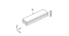
以下、本発明の実施の形態について図面を参照して詳細に説明する。始めに、図1を参照して、本発明の第1の実施の形態に係る磁気センサ装置を含む電流センサステムの構成について説明する。本実施の形態に係る磁気センサ装置1は、導体を流れる検出対象電流の値を検出する電流センサとして用いられる。図1には、検出対象電流が流れる導体がバスバー2である例を示している。磁気センサ装置1は、バスバー2の近傍に配置される。以下、検出対象電流を、対象電流Itgと記す。バスバー2の周囲には、対象電流Itgによって磁界3が発生する。磁気センサ装置1は、磁界3が印加される位置に配置されている。
[First embodiment]
Hereinafter, embodiments of the present invention will be described in detail with reference to the drawings. First, the configuration of a current sensor system including a magnetic sensor device according to a first embodiment of the present invention will be described with reference to FIG. 1. A
なお、バスバー2には、対象電流Itgによって発生する磁束を集める磁気コアが設けられていない。これにより、磁気センサ装置1を小型化することが可能になる。
The
次に、図1ないし図3を参照して、磁気センサ装置1の構成について詳しく説明する。図2は、磁気センサ装置1の構成を示すブロック図である。図3は、磁気センサを示す断面図である。磁気センサ装置1は、第1の検出回路5と、フィードバックコイル(以下、単にコイルと記す。)12と、第2の検出回路6と、制御回路23とを備えている。
Next, the configuration of the
第1の検出回路5は、印加磁界を検出する磁気検出素子を含み、印加磁界の強度と対応関係を有する第1の検出信号S1を生成する。ここで、対象電流Itgによって発生する磁界3のうち、第1の検出回路5の磁気検出素子に印加される磁界を、検出対象の磁界または対象磁界H1と言う。コイル12は、フィードバック電流Iccが流されることによって、対象磁界H1の少なくとも一部を相殺するためのキャンセル磁界H2を発生するためのものである。第2の検出回路6は、フィードバック電流Iccの値と対応関係を有する第2の検出信号S2を生成する。
The
制御回路23は、フィードバック電流Iccを制御すると共に対象磁界H1の強度と対応関係を有する検出値Vsを生成する。後で詳しく説明するが、制御回路23は、第1の検出信号S1または第2の検出信号S2に基づいて、検出値Vsを生成する。
The
磁気検出素子とコイル12を含む部分と、制御回路23を含む部分は、一体化されていてもよいし、別体であってもよい。本実施の形態では、上記2つの部分が別体となっている。以下、磁気検出素子とコイル12を含む部分を磁気センサ10と言い、制御回路23を含む部分をプロセッサ20と言う。磁気センサ10は、バスバー2とは独立している。プロセッサ20は、例えば特定用途向け集積回路(ASIC)あるいはマイクロコンピュータによって構成されている。プロセッサ20は、磁気センサ10に近接した位置に配置されていてもよいし、磁気センサ10から離れた位置に配置されていてもよい。
The part including the magnetic detection element and
図2に示したように、磁気センサ10は、コイル12の他に、ホイートストンブリッジ回路11と、抵抗器13とを含んでいる。ホイートストンブリッジ回路11は、それぞれ磁気検出素子を含む抵抗部R1,R2,R3,R4を含んでいる。
As shown in FIG. 2, the
図3に示したように、磁気センサ10は、更に、磁気検出素子(図3ではホイートストンブリッジ回路11)の近傍に設けられたシールド14を含んでいる。シールド14は、磁性材料よりなり、磁束を集める機能を有している。シールド14を設けることにより、磁気検出素子によって検出可能な印加磁界の強度の範囲を広げる、すなわちダイナミックレンジを大きくすることができる。ホイートストンブリッジ回路11、コイル12およびシールド14は、複数の絶縁層によって一体化されている。抵抗器13は、最も外側に位置する絶縁層の表面に取り付けられていてもよいし、複数の絶縁層に埋め込まれていてもよい。
As shown in FIG. 3, the
ここで、図1および図2に示したように、X方向、Y方向、Z方向を定義する。X方向、Y方向、Z方向は、互いに直交する。なお、本出願において、「直交」とは、完全に90°で直交することに加え、ほぼ直交すること、すなわち90°からわずかにずれて直交することも含む概念であるものとする。この本実施の形態では、図1に示した対象電流Itgが流れる方向をY方向とする。また、X方向とは反対の方向を-X方向とし、Y方向とは反対の方向を-Y方向とし、Z方向とは反対の方向を-Z方向とする。また、以下、基準の位置に対してZ方向の先にある位置を「上方」と言い、基準の位置に対して「上方」とは反対側にある位置を「下方」と言う。 Here, the X, Y, and Z directions are defined as shown in FIG. 1 and FIG. 2. The X, Y, and Z directions are mutually orthogonal. In this application, "orthogonal" is a concept that includes being almost orthogonal, i.e., being orthogonal with a slight deviation from 90 degrees, in addition to being completely orthogonal at 90 degrees. In this embodiment, the direction in which the target current Itg shown in FIG. 1 flows is the Y direction. Also, the direction opposite to the X direction is the -X direction, the direction opposite to the Y direction is the -Y direction, and the direction opposite to the Z direction is the -Z direction. Also, hereinafter, a position in the Z direction from the reference position is referred to as "upper", and a position opposite to the "upper" from the reference position is referred to as "lower".
磁気センサ10は、バスバー2の上方または下方に配置される。図1は、磁気センサ10を含む磁気センサ装置1が、バスバー2の上方に配置された例を示している。
The
図3に示したように、磁気センサ10は、更に、基板61と、絶縁層62,63,64,65,66,67,68とを含んでいる。絶縁層62,63,64は、基板61の上に積層されている。ホイートストンブリッジ回路11は、絶縁層64の上に配置されている。絶縁層65は、ホイートストンブリッジ回路11を覆うように、絶縁層64の上に配置されている。絶縁層66,67は、絶縁層65の上に積層されている。シールド14は、絶縁層67の上に配置されている。絶縁層68は、シールド14を覆うように、絶縁層67の上に配置されている。コイル12は、絶縁層63~66に埋め込まれている。
As shown in FIG. 3, the
図2に示したように、磁気センサ10は、ポートE11,E12,E13,E14,G1,P1,V1を有している。ホイートストンブリッジ回路11の抵抗部R1,R2の各一端は、ポートE11に接続されている。ホイートストンブリッジ回路11の抵抗部R3,R4の各一端は、ポートE12に接続されている。抵抗部R1,R3の各他端は、ポートV1に接続されている。抵抗部R2,R4の各他端は、ポートG1に接続されている。
As shown in FIG. 2, the
コイル12の一端は、ポートP1に接続されている。コイル12の他端と抵抗器13の一端は、ポートE13に接続されている。抵抗器13の他端は、ポートE14に接続されている。
One end of
図2に示したように、プロセッサ20は、ポートE20,E21,E22,E23,E24,G2,P2,V2を有している。ポートE21,E22,E23,E24,G2,P2,V2は、それぞれ、磁気センサ10のポートE11,E12,E13,E14,G1,P1,V1に接続されている。ポートV2には、磁気センサ10のホイートストンブリッジ回路11に供給するための、所定の大きさの電源電圧が印加される。ポートG2は、グランドに接続される。制御回路23は、ポートE20に対して検出値Vsを出力する。
As shown in FIG. 2, the
また、プロセッサ20は、制御回路23の他に、第1の増幅回路21と、第2の増幅回路22と、駆動回路24とを含んでいる。第1および第2の増幅回路21,22の各々は、2つの入力端と1つの出力端とを有している。第1の増幅回路21の2つの入力端は、それぞれポートE21,E22に接続されている。第2の増幅回路22の2つの入力端は、それぞれポートE23,E24に接続されている。第1の増幅回路21の出力端と第2の増幅回路22の出力端は、制御回路23に接続されている。
The
駆動回路24は、コイル12に対してフィードバック電流Iccを供給する回路である。制御回路23は、駆動回路24を制御することによって、フィードバック電流Iccを制御する。フィードバック電流Iccは、ポートP1,P2を介してコイル12に供給される。
The
第1の検出回路5は、磁気センサ10のホイートストンブリッジ回路11と、プロセッサ20の第1の増幅回路21とによって構成されている。第2の検出回路6は、磁気センサ10の抵抗器13と、プロセッサ20の第2の増幅回路22とによって構成されている。
The
次に、第1の検出回路5に含まれる磁気検出素子について説明する。磁気検出素子は、ホール素子であってもよいし、磁気抵抗効果素子であってもよい。しかし、応答速度の観点から、磁気検出素子は、磁気抵抗効果素子であることが好ましい。以下、磁気抵抗効果素子を、MR素子と記す。MR素子は、スピンバルブ型のMR素子でもよいし、AMR(異方性磁気抵抗効果)素子でもよい。本実施の形態では特に、第1の検出回路5は、磁気検出素子として、スピンバルブ型のMR素子50を含んでいる。
Next, the magnetic detection element included in the
図4は、MR素子50を示す斜視図である。MR素子50は、方向が固定された磁化を有する磁化固定層52と、印加磁界の方向に応じて方向が変化可能な磁化を有する自由層54と、磁化固定層52と自由層54の間に配置されたギャップ層53とを含んでいる。MR素子50は、TMR(トンネル磁気抵抗効果)素子でもよいし、GMR(巨大磁気抵抗効果)素子でもよいが、応答速度および精度の観点から、TMR素子であることが好ましい。TMR素子では、ギャップ層53はトンネルバリア層である。GMR素子では、ギャップ層53は非磁性導電層である。MR素子50では、自由層54の磁化の方向が磁化固定層52の磁化の方向に対してなす角度に応じて抵抗値が変化し、この角度が0°のときに抵抗値は最小値となり、角度が180°のときに抵抗値は最大値となる。MR素子50において、自由層54は、磁化容易軸方向が、磁化固定層52の磁化の方向に直交する方向となる形状異方性を有している。
Figure 4 is a perspective view showing an
MR素子50は、更に、反強磁性層51を含んでいる。反強磁性層51、磁化固定層52、ギャップ層53および自由層54は、この順に積層されている。なお、MR素子50における層51~54の配置は、図4に示した配置とは上下が反対でもよい。反強磁性層51は、反強磁性材料よりなり、磁化固定層52との間で交換結合を生じさせて、磁化固定層52の磁化の方向を固定する。なお、磁化固定層52は、いわゆるセルフピン止め型の固定層(Synthetic Ferri Pinned層、SFP層)であってもよい。セルフピン止め型の固定層は、強磁性層、非磁性中間層および強磁性層を積層させた積層フェリ構造を有し、2つの強磁性層を反強磁性的に結合させてなるものである。磁化固定層52がセルフピン止め型の固定層である場合、反強磁性層51を省略してもよい。
The
ホイートストンブリッジ回路11の抵抗部R1~R4の各々は、少なくとも1つのMR素子50を含んでいる。抵抗部R1,R4の各々におけるMR素子50の磁化固定層52の磁化の方向は第1の磁化方向である。抵抗部R2,R3の各々におけるMR素子50の磁化固定層52の磁化の方向は、第1の磁化方向とは反対方向の第2の磁化方向である。
Each of the resistance parts R1 to R4 of the
次に、磁気センサ10の位置および姿勢について説明する。磁気センサ10には、対象電流Itgによって発生する磁界3とコイル12が発生する磁界が印加される。磁気センサ10は、印加される上記の2つの磁界の方向が互いに反対方向またはほぼ反対方向になる位置に配置されている。
Next, the position and orientation of the
ここで、磁気センサ10に印加される上記の2つの磁界の方向に平行な方向を、感磁方向と言う。対象磁界H1は、対象電流Itgによって発生して磁気センサ10に印加される磁界3の、感磁方向に平行な方向の成分である。また、キャンセル磁界H2は、コイル12が発生して磁気センサ10に印加される磁界の、感磁方向に平行な方向の成分である。
Here, the direction parallel to the directions of the above two magnetic fields applied to the
一般的に、平面ホール素子は、基板に対して垂直な感度軸を有する傾向があり、MR素子や垂直ホール素子は、基板に対して平行な感度軸を有する傾向がある。MR素子がTMR素子またはGMR素子の場合には、一般的に、磁化固定層の磁化方向に平行な方向を感磁方向とする。従って、MR素子50がTMR素子またはGMR素子の場合、磁気センサ10は、第1および第2の磁化方向が、感磁方向に平行またはほぼ平行になる姿勢で配置される。
In general, planar Hall elements tend to have a sensitivity axis perpendicular to the substrate, while MR elements and vertical Hall elements tend to have a sensitivity axis parallel to the substrate. When the MR element is a TMR element or a GMR element, the magnetic sensing direction is generally parallel to the magnetization direction of the magnetization pinned layer. Therefore, when the
ここで、対象磁界H1の方向とキャンセル磁界H2の方向を、X方向に平行な方向とする。この場合、磁気センサ10は、例えば、第1の磁化方向がX方向になり、第2の磁化方向が-X方向になるような姿勢で配置される。なお、第1および第2の磁化方向は、MR素子50の作製の精度および磁気センサ10のアライメントの精度等の観点から、上述の方向からわずかにずれていてもよい。
Here, the direction of the target magnetic field H1 and the direction of the cancellation magnetic field H2 are parallel to the X direction. In this case, the
MR素子50の自由層54は、感磁方向と交差する方向を容易軸とする形状異方性を有することが好ましい。また、MR素子50の自由層54に対してバイアス磁界を印加する磁石を設けることにより、感磁方向と交差する方向を容易軸とすることができる。
The
次に、制御回路23の動作について説明する。制御回路23は、クローズドループ動作とオープンループ動作とを選択可能である。クローズドループ動作は、制御回路23が、第1の検出信号S1が一定値になるようにフィードバック電流Iccを制御する動作である。オープンループ動作は、制御回路23が、フィードバック電流Iccを一定値に維持する動作である。クローズドループ動作の実行時には、磁気センサ装置1が磁気平衡方式の電流センサとして動作する。オープンループ動作の実行時には、磁気センサ装置1が磁気比例方式の電流センサとして動作する。
Next, the operation of the
印加磁界の強度が変化すると、磁気センサ10のポートE11,E12間の電位差が変化する。これにより、プロセッサ20のポートE21,E22間の電位差が変化する。第1の増幅回路21は、ポートE21,E22間の電位差に対応する信号を、第1の検出信号S1として出力する。ノイズ磁界が存在しない場合には、印加磁界は、対象磁界H1とキャンセル磁界H2との残差の磁界(以下、残差磁界と言う。)である。制御回路23は、クローズドループ動作の実行時には、残差磁界の強度がゼロに近づくように、第1の検出信号S1の値に応じて、フィードバック電流Iccを制御する。これにより、クローズドループ動作の実行時には、第1の検出信号S1の値は、一定値(例えばゼロ)に維持される。
When the strength of the applied magnetic field changes, the potential difference between ports E11 and E12 of the
フィードバック電流Iccの値が変化すると、磁気センサ10のポートE13,E14間の電位差が変化する。これにより、プロセッサ20のポートE23,E24間の電位差が変化する。第2の増幅回路22は、ポートE23,E24間の電位差に対応する信号を、第2の検出信号S2として出力する。クローズドループ動作の実行時には、第2の検出信号S2の値は、対象磁界H1の強度および対象電流Itgの値と対応関係を有する。制御回路23は、クローズドループ動作の実行時には、第2の検出信号S2に基づいて検出値Vsを生成する。検出値Vsは、例えば、第2の検出信号S2に対してゲイン調整およびオフセット調整等の所定の補正を加えることによって生成される。
When the value of the feedback current Icc changes, the potential difference between ports E13 and E14 of the
オープンループ動作の実行時には、制御回路23は、フィードバック電流Iccを一定値に維持する。そのため、オープンループ動作の実行時には、残差磁界の強度は、対象磁界H1の強度に応じて変化する。オープンループ動作の実行時には、第1の検出信号S1の値は、対象磁界H1の強度および対象電流Itgの値と対応関係を有する。制御回路23は、オープンループ動作の実行時には、第1の検出信号S1に基づいて検出値Vsを生成する。検出値Vsは、例えば、第1の検出信号S1に対してゲイン調整およびオフセット調整等の所定の補正を加えることによって生成される。
When open-loop operation is performed, the
本実施の形態では特に、制御回路23は、対象磁界H1の強度が第1の値よりも大きく第2の値未満の場合にはクローズドループ動作を実行し、対象磁界H1の強度が第1の値以下または第2の値以上の場合にはオープンループ動作を実行するように構成されている。クローズドループ動作の実行時には、制御回路23は、残差磁界の強度がゼロになるように、すなわちキャンセル磁界H2によって対象磁界H1が完全に相殺されるように、フィードバック電流Iccを制御する。オープンループ動作の実行時には、制御回路23は、キャンセル磁界H2によって対象磁界H1の一部が相殺されるように、フィードバック電流Iccを一定値に維持する。
In particular, in this embodiment, the
ここで、磁界の方向がX方向になるときの磁界の強度を正の値で表し、磁界の方向が-X方向になるときの磁界の強度を負の値で表す。本実施の形態では、第1の値は負の値であり、第2の値は正の値である。 Here, the strength of the magnetic field when its direction is in the X direction is represented by a positive value, and the strength of the magnetic field when its direction is in the -X direction is represented by a negative value. In this embodiment, the first value is a negative value, and the second value is a positive value.
図5は、対象磁界H1の強度とフィードバック電流Iccとの関係を示す特性図である。図5において、横軸は対象磁界H1の強度を示し、縦軸はフィードバック電流Iccを示している。なお、図5では、対象磁界H1の強度を、対象磁界H1の強度に対応する磁束密度の値で示している。以下の説明では、磁界の強度を、磁界の強度に対応する磁束密度の値で表す。また、対象磁界H1の方向が-X方向(キャンセル磁界H2の方向がX方向)の場合、コイル12を流れるフィードバック電流Iccの方向は、対象磁界H1の方向がX方向(キャンセル磁界H2の方向が-X方向)の場合とは反対方向になる。しかし、図5では、フィードバック電流Iccの方向に関わらず、フィードバック電流Iccの値を正の値で示している。
Figure 5 is a characteristic diagram showing the relationship between the strength of the target magnetic field H1 and the feedback current Icc. In Figure 5, the horizontal axis indicates the strength of the target magnetic field H1, and the vertical axis indicates the feedback current Icc. In Figure 5, the strength of the target magnetic field H1 is shown as a value of magnetic flux density corresponding to the strength of the target magnetic field H1. In the following explanation, the strength of the magnetic field is represented by a value of magnetic flux density corresponding to the strength of the magnetic field. In addition, when the direction of the target magnetic field H1 is the -X direction (the direction of the cancel magnetic field H2 is the X direction), the direction of the feedback current Icc flowing through the
図5に示した例では、第1の値を-10mTとし、第2の値を10mTとしている。図5に示したように、対象磁界H1の強度が0から大きくなる場合、対象磁界H1の強度が10mTに達するまでは、対象磁界H1の強度が大きくなるに従って、フィードバック電流Iccが大きくなる。対象磁界H1の強度が10mT以上になると、フィードバック電流Iccは、一定値に維持される。制御回路23は、対象磁界H1の強度が10mT以上になる場合、キャンセル磁界H2の強度の絶対値が第2の値の絶対値(10mT)と等しくなるように、フィードバック電流Iccを一定値に維持する。
In the example shown in FIG. 5, the first value is -10 mT and the second value is 10 mT. As shown in FIG. 5, when the strength of the target magnetic field H1 increases from 0, the feedback current Icc increases as the strength of the target magnetic field H1 increases until the strength of the target magnetic field H1 reaches 10 mT. When the strength of the target magnetic field H1 becomes 10 mT or more, the feedback current Icc is maintained at a constant value. When the strength of the target magnetic field H1 becomes 10 mT or more, the
同様に、対象磁界H1の強度が0から小さくなる場合、対象磁界H1の強度が-10mTに達するまでは、対象磁界H1の強度が小さくなるに従って、フィードバック電流Iccが大きくなる。対象磁界H1の強度が-10mT以下になると、フィードバック電流Iccは、一定値に維持される。制御回路23は、対象磁界H1の強度が-10mT以下になる場合、キャンセル磁界H2の強度の絶対値が第1の値の絶対値(10mT)と等しくなるように、フィードバック電流Iccを一定値に維持する。
Similarly, when the strength of the target magnetic field H1 decreases from 0, the feedback current Icc increases as the strength of the target magnetic field H1 decreases until the strength of the target magnetic field H1 reaches -10 mT. When the strength of the target magnetic field H1 becomes -10 mT or less, the feedback current Icc is maintained at a constant value. When the strength of the target magnetic field H1 becomes -10 mT or less, the
図6は、対象磁界H1の強度と第2の検出信号S2との関係を示す特性図である。図6において、横軸は対象磁界H1の強度を示し、縦軸は第2の検出信号S2を示している。図6に示したように、対象磁界H1の強度が-10mTよりも大きく10mT未満の場合には、第2の検出信号S2は、対象磁界H1の強度に応じて変化する。対象磁界H1の強度が-10mT以下または10mT以上の場合には、第2の検出信号S2は、対象磁界H1の強度に関わらず一定値になる。 Figure 6 is a characteristic diagram showing the relationship between the strength of the target magnetic field H1 and the second detection signal S2. In Figure 6, the horizontal axis represents the strength of the target magnetic field H1, and the vertical axis represents the second detection signal S2. As shown in Figure 6, when the strength of the target magnetic field H1 is greater than -10 mT and less than 10 mT, the second detection signal S2 changes according to the strength of the target magnetic field H1. When the strength of the target magnetic field H1 is less than -10 mT or greater than 10 mT, the second detection signal S2 has a constant value regardless of the strength of the target magnetic field H1.
図7は、対象磁界H1の強度と第1の検出信号S1との関係を示す特性図である。図7において、横軸は対象磁界H1の強度を示し、縦軸は第1の検出信号S1を示している。図7に示したように、対象磁界H1の強度が-10mTよりも大きく10mT未満の場合には、第1の検出信号S1は、対象磁界H1の強度に関わらず一定値になる。対象磁界H1の強度が-10mT以下または10mT以上の場合には、第1の検出信号S1は、対象磁界H1の強度に応じて変化する。 Figure 7 is a characteristic diagram showing the relationship between the strength of the target magnetic field H1 and the first detection signal S1. In Figure 7, the horizontal axis represents the strength of the target magnetic field H1, and the vertical axis represents the first detection signal S1. As shown in Figure 7, when the strength of the target magnetic field H1 is greater than -10 mT and less than 10 mT, the first detection signal S1 has a constant value regardless of the strength of the target magnetic field H1. When the strength of the target magnetic field H1 is less than -10 mT or greater than 10 mT, the first detection signal S1 changes depending on the strength of the target magnetic field H1.
なお、オープンループ動作の実行時の対象磁界H1の強度の変化に対する第1の検出信号S1の変化の勾配は、クローズドループ動作の実行時の対象磁界H1の強度の変化に対する第2の検出信号S2の変化の勾配とは異なっていてもよい。図6および図7に示した例では、オープンループ動作の実行時の対象磁界H1の強度の変化に対する第1の検出信号S1の変化の勾配は、クローズドループ動作の実行時の対象磁界H1の強度の変化に対する第2の検出信号S2の変化の勾配よりも小さい。 The gradient of the change in the first detection signal S1 with respect to the change in the intensity of the target magnetic field H1 when the open-loop operation is performed may be different from the gradient of the change in the second detection signal S2 with respect to the change in the intensity of the target magnetic field H1 when the closed-loop operation is performed. In the examples shown in Figures 6 and 7, the gradient of the change in the first detection signal S1 with respect to the change in the intensity of the target magnetic field H1 when the open-loop operation is performed is smaller than the gradient of the change in the second detection signal S2 with respect to the change in the intensity of the target magnetic field H1 when the closed-loop operation is performed.
次に、本実施の形態に係る磁気センサ装置1の作用および効果について説明する。本実施の形態では、制御回路23は、対象磁界H1の強度が第1の値よりも大きく第2の値未満の場合にはクローズドループ動作を実行するように構成されている。すなわち、本実施の形態では、対象磁界H1の強度の絶対値が小さくなる領域では、磁気センサ装置1が磁気平衡方式の電流センサとして動作するように構成されている。これにより、本実施の形態によれば、対象磁界H1の強度が小さくなる領域において、精度よく対象電流Itgを検出することが可能になる。クローズドループ動作の実行時には、第2の検出信号S2は、磁気平衡方式の電流センサの検出値に相当する。
Next, the action and effect of the
また、本実施の形態では、制御回路23は、対象磁界H1の強度が第1の値以下または第2の値以上の場合にはオープンループ動作を実行するように構成されている。すなわち、本実施の形態では、対象磁界H1の強度の絶対値が大きくなる領域では、磁気センサ装置1が磁気比例方式の電流センサとして動作するように構成されている。これにより、本実施の形態によれば、対象電流Itgの測定範囲を広げることができる。オープンループ動作の実行時の第1の検出信号S1は、磁気比例方式の電流センサの検出値に相当する。
In addition, in this embodiment, the
また、本実施の形態によれば、瞬間的に強度が変化するノイズ磁界(パルス状のノイズ磁界)を検出することができる。以下、この効果について、図8および図9を参照して説明する。図8は、印加磁界とパルス状のノイズ磁界を示す模式図である。図8(a)は、パルス状のノイズ磁界が重畳した印加磁界を示している。図8(b)は、パルス状のノイズ磁界を拡大して示している。 Furthermore, according to this embodiment, it is possible to detect a noise magnetic field (a pulsed noise magnetic field) whose strength changes instantaneously. This effect will be described below with reference to Figs. 8 and 9. Fig. 8 is a schematic diagram showing an applied magnetic field and a pulsed noise magnetic field. Fig. 8(a) shows an applied magnetic field superimposed with a pulsed noise magnetic field. Fig. 8(b) shows an enlarged view of the pulsed noise magnetic field.
図9は、印加磁界にパルス状のノイズ磁界が重畳したときの第1および第2の検出信号S1,S2を示す模式図である。図9(a)は、第2の検出信号S2を示している。図9(b)は、第1の検出信号S1を示している。なお、図9(a)では、ノイズ磁界が存在しない場合における第2の検出信号S2の最大値が1になり、ノイズ磁界が存在しない場合における第2の検出信号S2の最小値が-1になるように、第2の検出信号S2を規格化している。また、図9(b)では、ノイズ磁界が存在しない場合における第1の検出信号S1の最大値が1になり、ノイズ磁界が存在しない場合における第1の検出信号S1の最小値が-1になるように、第1の検出信号S1を規格化している。 Figure 9 is a schematic diagram showing the first and second detection signals S1 and S2 when a pulsed noise magnetic field is superimposed on the applied magnetic field. Figure 9(a) shows the second detection signal S2. Figure 9(b) shows the first detection signal S1. In Figure 9(a), the second detection signal S2 is normalized so that the maximum value of the second detection signal S2 when no noise magnetic field exists is 1, and the minimum value of the second detection signal S2 when no noise magnetic field exists is -1. In Figure 9(b), the first detection signal S1 is normalized so that the maximum value of the first detection signal S1 when no noise magnetic field exists is 1, and the minimum value of the first detection signal S1 when no noise magnetic field exists is -1.
図8および図9には、クローズドループ動作の実行時に、瞬間的に印加磁界の強度を大きくするパルス状のノイズ磁界が発生した例を示している。第2の検出信号S2は、フィードバック電流Iccに応じて変化する。フィードバック電流Iccは、制御回路23および駆動回路24によって制御される。そのため、第2の検出信号S2は、原理上、応答速度が遅くなる。そのため、図9(a)に示したように、パルス状のノイズ磁界が重畳しても、第2の検出信号S2は、ほとんど変化しない。
Figures 8 and 9 show an example in which a pulsed noise magnetic field occurs during closed-loop operation, momentarily increasing the strength of the applied magnetic field. The second detection signal S2 changes according to the feedback current Icc. The feedback current Icc is controlled by the
一方、第1の検出信号S1は、制御回路23および駆動回路24による制御が割り込まないため、第2の検出信号S2に比べて応答速度が速くなる。本実施の形態では特に、磁気検出素子として、応答速度が速く高精度のMR素子50(TMR素子)を用いている。そのため、図9(a)に示したように、パルス状のノイズ磁界が重畳すると、パルス状のノイズ磁界に応じて第1の検出信号S1の値が変化する。図示しないが、オープンループ動作の実行時に、パルス状のノイズ磁界が重畳した場合にも、パルス状のノイズ磁界に応じて第1の検出信号S1の値が変化する。従って、第1の検出信号S1を監視することによって、パルス状のノイズ磁界を検出することが可能になる。
On the other hand, the first detection signal S1 has a faster response speed than the second detection signal S2 because the control by the
制御回路23は、ポートE20または図示しないポートに対してパルス状のノイズ磁界を検出したことを示す信号Spを出力することができるように構成されていてもよい。
The
なお、図8および図9には、印加磁界の強度が大きくなるパルス状のノイズ磁界が重畳する場合を示している。しかし、図8および図9を参照した一連の説明は、印加磁界の強度が小さくなるパルス状のノイズ磁界が重畳する場合にも当てはまる。 Note that Figures 8 and 9 show a case where a pulsed noise magnetic field that increases the strength of the applied magnetic field is superimposed. However, the series of explanations referring to Figures 8 and 9 also apply to a case where a pulsed noise magnetic field that decreases the strength of the applied magnetic field is superimposed.
パルス状のノイズ磁界が、瞬間的に印加磁界の強度を大きくする磁界である場合、パルス状のノイズ磁界の強度の最大値は、第2の値よりも大きくてもよい。同様に、パルス状のノイズ磁界が、瞬間的に印加磁界の強度を小さくする磁界である場合、パルス状のノイズ磁界の強度の最小値は、第1の値よりも小さくてもよい。 When the pulsed noise magnetic field is a magnetic field that momentarily increases the strength of the applied magnetic field, the maximum value of the strength of the pulsed noise magnetic field may be greater than the second value. Similarly, when the pulsed noise magnetic field is a magnetic field that momentarily decreases the strength of the applied magnetic field, the minimum value of the strength of the pulsed noise magnetic field may be less than the first value.
また、本実施の形態では特に、クローズドループ動作の実行時には、制御回路23は、第1の検出信号S1が一定値になるようにフィードバック電流Iccを制御している。そのため、本実施の形態によれば、対象磁界H1に応じて変化する信号に基づいてパルス状のノイズ磁界を検出する場合に比べて、強度の小さなパルス状のノイズ磁界を検出することが容易になる。
In particular, in this embodiment, when closed-loop operation is being performed, the
また、図6および図7に示した例のように、オープンループ動作の実行時の対象磁界H1の強度の変化に対する第1の検出信号S1の変化の勾配は、クローズドループ動作の実行時の対象磁界H1の強度の変化に対する第2の検出信号S2の変化の勾配よりも小さくてもよい。これによっても、強度の小さなパルス状のノイズ磁界を検出することが容易になる。 Also, as in the examples shown in Figures 6 and 7, the gradient of the change in the first detection signal S1 relative to the change in the intensity of the target magnetic field H1 during open-loop operation may be smaller than the gradient of the change in the second detection signal S2 relative to the change in the intensity of the target magnetic field H1 during closed-loop operation. This also makes it easier to detect a pulse-like noise magnetic field with a small intensity.
なお、パルス状のノイズ磁界を検出するために、制御回路23は、第1の検出信号S1に加えて、あるいは第1の検出信号S1の代わりに、第1の検出信号S1と第2の検出信号S2とを合成して得られる信号を用いてもよい。
In addition, to detect a pulsed noise magnetic field, the
次に、本実施の形態に係るインバータ装置およびバッテリ装置について説明する。ここでは、電動モータを使用した車両に用いられるインバータ装置およびバッテリ装置を例にとって説明する。図10は、インバータ装置およびバッテリ装置の構成を示すブロック図である。図10に示したように、電動モータ101には、電動モータ101を制御するインバータ装置102が接続されている。インバータ装置102には、バッテリ装置103が接続されている。バッテリ装置103は、インバータ装置102を介して電動モータ101に高電圧の電力を供給する。また、インバータ装置102には、ECU(Electronic Control Unit)104が接続されている。
Next, an inverter device and a battery device according to this embodiment will be described. Here, an inverter device and a battery device used in a vehicle using an electric motor will be described as an example. FIG. 10 is a block diagram showing the configuration of the inverter device and the battery device. As shown in FIG. 10, an
インバータ装置102は、インバータ回路121と、磁気センサ装置1Aとを備えている。インバータ回路121は、検出対象電流が流れる導体を含んでいる。磁気センサ装置1Aは、インバータ回路121の導体を流れる検出対象電流を検出して、この検出対象電流と対応関係を有する検出値を生成する。磁気センサ装置1Aの構成は、図1ないし図4を参照して説明した磁気センサ装置1の構成と同様である。
The
バッテリ装置103は、電源回路131と、バッテリ132と、磁気センサ装置1Bとを備えている。電源回路131は、検出対象電流が流れる導体を含んでいる。磁気センサ装置1Bは、電源回路131の導体を流れる検出対象電流を検出して、この検出対象電流と対応関係を有する検出値を生成する。磁気センサ装置1Bの構成は、図1ないし図4を参照して説明した磁気センサ装置1の構成と同様である。
The
[第2の実施の形態]
次に、本発明の第2の実施の形態について説明する。図11は、本実施の形態に係る磁気センサ装置の磁気センサを示す断面図である。本実施の形態に係る磁気センサ装置1は、第1の実施の形態における磁気センサ10の代わりに、磁気センサ110を備えている。磁気センサ110には、第1の実施の形態におけるシールド14および絶縁層68が設けられていない。代わりに、磁気センサ110は、絶縁層67の上に配置された絶縁層69を含んでいる。磁気センサ110のその他の構成は、第1の実施の形態における磁気センサ10の構成と同じである。
[Second embodiment]
Next, a second embodiment of the present invention will be described. Fig. 11 is a cross-sectional view showing a magnetic sensor of a magnetic sensor device according to this embodiment. The
本実施の形態では、シールド14が設けられていない。これにより、本実施の形態によれば、対象磁界H1および印加磁界の各々の強度の変化に対する第1の検出信号S1の変化の勾配を大きくすることができる。これにより、本実施の形態によれば、より効果的に、パルス状のノイズ磁界を検出することが可能になる。
In this embodiment, the
本実施の形態におけるその他の構成、作用および効果は、第1の実施の形態と同様である。 The other configurations, actions, and effects of this embodiment are the same as those of the first embodiment.
なお、本発明は、上記各実施の形態に限定されず、種々の変更が可能である。例えば、本発明の磁気センサ装置は、対象磁界が、電流によって発生するものではない場合にも適用することができる。 The present invention is not limited to the above-described embodiments, and various modifications are possible. For example, the magnetic sensor device of the present invention can be applied to cases where the target magnetic field is not generated by a current.
1…磁気センサ装置、2…バスバー、3…磁界、5…第1の検出回路、6…第2の検出回路、10…磁気センサ、11…ホイートストンブリッジ回路、12…フィードバックコイル、13…抵抗器、14…シールド、20…プロセッサ、21…第1の増幅回路、22…第2の増幅回路、23…制御回路、24…駆動回路、50…MR素子、101…電動モータ、102…インバータ装置、103…バッテリ装置、121…インバータ回路、131…電源回路、132…バッテリ。 1...magnetic sensor device, 2...bus bar, 3...magnetic field, 5...first detection circuit, 6...second detection circuit, 10...magnetic sensor, 11...Wheatstone bridge circuit, 12...feedback coil, 13...resistor, 14...shield, 20...processor, 21...first amplifier circuit, 22...second amplifier circuit, 23...control circuit, 24...drive circuit, 50...MR element, 101...electric motor, 102...inverter device, 103...battery device, 121...inverter circuit, 131...power supply circuit, 132...battery.
Claims (18)
フィードバック電流が流されることによって、検出対象の磁界である対象磁界の少なくとも一部を相殺するためのキャンセル磁界を発生するフィードバックコイルと、
前記フィードバック電流の値と対応関係を有する第2の検出信号を生成する第2の検出回路とを備え、
前記対象磁界の強度が第1の値よりも大きく第2の値未満の第1の場合には前記第1の検出信号が一定値になるように前記フィードバック電流が制御され、前記対象磁界の強度が前記第1の値以下または前記第2の値以上の第2の場合には前記キャンセル磁界によって前記対象磁界の一部を相殺するために前記フィードバック電流が一定値になるように制御され、
前記第1の場合には、前記第2の検出信号に基づいて生成された検出値が前記対象磁界の強度と対応関係を有し、前記第2の場合には、前記第1の検出信号に基づいて生成された検出値が前記対象磁界の強度と対応関係を有することを特徴とする磁気センサ装置。 a first detection circuit including a magnetic detection element for detecting an applied magnetic field and for generating a first detection signal having a corresponding relationship with the intensity of the applied magnetic field;
a feedback coil that generates a cancellation magnetic field for canceling at least a part of a target magnetic field that is a magnetic field to be detected by flowing a feedback current therethrough;
a second detection circuit that generates a second detection signal having a corresponding relationship with a value of the feedback current;
In a first case where the intensity of the target magnetic field is greater than a first value and less than a second value, the feedback current is controlled so that the first detection signal has a constant value, and in a second case where the intensity of the target magnetic field is equal to or less than the first value or equal to or greater than the second value, the feedback current is controlled to a constant value in order to cancel a portion of the target magnetic field with the cancellation magnetic field ;
A magnetic sensor device characterized in that in the first case, a detection value generated based on the second detection signal has a corresponding relationship with the intensity of the target magnetic field, and in the second case, a detection value generated based on the first detection signal has a corresponding relationship with the intensity of the target magnetic field.
フィードバック電流が流されることによって、検出対象の磁界である対象磁界の少なくとも一部を相殺するためのキャンセル磁界を発生するフィードバックコイルと、
前記フィードバック電流の値と対応関係を有する第2の検出信号を生成する第2の検出回路とを備え、
前記対象磁界の強度が第1の値よりも大きく第2の値未満の第1の場合には前記第1の検出信号が一定値になるように前記フィードバック電流が制御され、前記対象磁界の強度が前記第1の値以下または前記第2の値以上の第2の場合には前記フィードバック電流が一定値になるように制御され、
前記第1の場合には、前記第2の検出信号に基づいて生成された検出値が前記対象磁界の強度と対応関係を有し、前記第2の場合には、前記第1の検出信号に基づいて生成された検出値が前記対象磁界の強度と対応関係を有し、
前記フィードバック電流は、前記第2の場合には、前記キャンセル磁界の強度の絶対値が前記第1の値の絶対値または前記第2の値の絶対値と等しくなるように、前記一定値に維持されることを特徴とする磁気センサ装置。 a first detection circuit including a magnetic detection element for detecting an applied magnetic field and for generating a first detection signal having a corresponding relationship with the intensity of the applied magnetic field;
a feedback coil that generates a cancellation magnetic field for canceling at least a part of a target magnetic field that is a magnetic field to be detected by flowing a feedback current therethrough;
a second detection circuit that generates a second detection signal having a corresponding relationship with a value of the feedback current;
The feedback current is controlled so that the first detection signal becomes a constant value in a first case where the intensity of the target magnetic field is greater than a first value and less than a second value, and the feedback current is controlled so that the first detection signal becomes a constant value in a second case where the intensity of the target magnetic field is equal to or less than the first value or equal to or greater than the second value,
In the first case, a detection value generated based on the second detection signal has a corresponding relationship with the intensity of the target magnetic field, and in the second case, a detection value generated based on the first detection signal has a corresponding relationship with the intensity of the target magnetic field;
The magnetic sensor device characterized in that, in the second case, the feedback current is maintained at the constant value so that the absolute value of the strength of the canceling magnetic field is equal to the absolute value of the first value or the absolute value of the second value.
前記制御回路は、前記第1の検出信号、または前記第1の検出信号と前記第2の検出信号の両方を用いて、ノイズ磁界を検出するように構成されていることを特徴とする請求項1ないし4のいずれかに記載の磁気センサ装置。 Further, a control circuit is provided,
5. The magnetic sensor device according to claim 1, wherein the control circuit is configured to detect a noise magnetic field using the first detection signal or both the first detection signal and the second detection signal.
前記検出値は、前記検出対象電流と対応関係を有することを特徴とする請求項1ないし10のいずれかに記載の磁気センサ装置。 the target magnetic field is a magnetic field generated by a target current flowing through a conductor,
11. The magnetic sensor device according to claim 1, wherein the detection value has a correspondence relationship with the current to be detected.
前記導体を含むインバータ回路とを備えたことを特徴とするインバータ装置。 A magnetic sensor device according to claim 11 or 12,
and an inverter circuit including the conductor.
電動モータとを備えた車両であって、
前記インバータ装置は、前記電動モータを制御するように構成されていることを特徴とする車両。 An inverter device according to claim 13;
A vehicle equipped with an electric motor,
The inverter device is configured to control the electric motor.
前記導体を含む電源回路と、
前記電源回路に接続されたバッテリとを備えたことを特徴とするバッテリ装置。 A magnetic sensor device according to claim 11 or 12,
a power supply circuit including the conductor;
a battery connected to the power supply circuit.
電動モータとを備えた車両であって、
前記バッテリ装置は、前記電動モータに電流を供給するように構成されていることを特徴とする車両。
The battery device according to claim 16,
A vehicle equipped with an electric motor,
The vehicle, wherein the battery device is configured to supply current to the electric motor.
Priority Applications (1)
| Application Number | Priority Date | Filing Date | Title |
|---|---|---|---|
| JP2023070123A JP7607071B2 (en) | 2021-03-08 | 2023-04-21 | Magnetic sensor device, inverter device, battery device, electric motor and vehicle |
Applications Claiming Priority (2)
| Application Number | Priority Date | Filing Date | Title |
|---|---|---|---|
| JP2021036337A JP7273876B2 (en) | 2021-03-08 | 2021-03-08 | Magnetic sensor device, inverter device and battery device |
| JP2023070123A JP7607071B2 (en) | 2021-03-08 | 2023-04-21 | Magnetic sensor device, inverter device, battery device, electric motor and vehicle |
Related Parent Applications (1)
| Application Number | Title | Priority Date | Filing Date |
|---|---|---|---|
| JP2021036337A Division JP7273876B2 (en) | 2021-03-08 | 2021-03-08 | Magnetic sensor device, inverter device and battery device |
Publications (2)
| Publication Number | Publication Date |
|---|---|
| JP2023084140A JP2023084140A (en) | 2023-06-16 |
| JP7607071B2 true JP7607071B2 (en) | 2024-12-26 |
Family
ID=82898390
Family Applications (2)
| Application Number | Title | Priority Date | Filing Date |
|---|---|---|---|
| JP2021036337A Active JP7273876B2 (en) | 2021-03-08 | 2021-03-08 | Magnetic sensor device, inverter device and battery device |
| JP2023070123A Active JP7607071B2 (en) | 2021-03-08 | 2023-04-21 | Magnetic sensor device, inverter device, battery device, electric motor and vehicle |
Family Applications Before (1)
| Application Number | Title | Priority Date | Filing Date |
|---|---|---|---|
| JP2021036337A Active JP7273876B2 (en) | 2021-03-08 | 2021-03-08 | Magnetic sensor device, inverter device and battery device |
Country Status (4)
| Country | Link |
|---|---|
| US (2) | US11619659B2 (en) |
| JP (2) | JP7273876B2 (en) |
| CN (1) | CN115047384A (en) |
| DE (1) | DE102021133302A1 (en) |
Families Citing this family (2)
| Publication number | Priority date | Publication date | Assignee | Title |
|---|---|---|---|---|
| JP7452883B2 (en) * | 2019-08-06 | 2024-03-19 | 株式会社 Integral Geometry Science | Storage battery inspection device and storage battery inspection method |
| TWI844114B (en) | 2022-09-22 | 2024-06-01 | 愛盛科技股份有限公司 | Magnetic field sensing device |
Citations (3)
| Publication number | Priority date | Publication date | Assignee | Title |
|---|---|---|---|---|
| JP2007078416A (en) | 2005-09-12 | 2007-03-29 | Denso Corp | Current sensor and current sensing method |
| WO2011105209A1 (en) | 2010-02-23 | 2011-09-01 | アルプス・グリーンデバイス株式会社 | Current sensor |
| WO2011136057A1 (en) | 2010-04-26 | 2011-11-03 | アルプス・グリーンデバイス株式会社 | Current sensor |
Family Cites Families (9)
| Publication number | Priority date | Publication date | Assignee | Title |
|---|---|---|---|---|
| JP2011169833A (en) * | 2010-02-19 | 2011-09-01 | Stanley Electric Co Ltd | Current sensor |
| JP5699301B2 (en) * | 2010-02-23 | 2015-04-08 | アルプス・グリーンデバイス株式会社 | Current sensor |
| CN102959408A (en) * | 2010-07-07 | 2013-03-06 | 阿尔卑斯绿色器件株式会社 | Current sensor |
| WO2012011306A1 (en) * | 2010-07-20 | 2012-01-26 | アルプス・グリーンデバイス株式会社 | Current sensor |
| JP5531214B2 (en) * | 2010-08-31 | 2014-06-25 | アルプス・グリーンデバイス株式会社 | Current sensor |
| JP6969142B2 (en) * | 2017-04-12 | 2021-11-24 | Tdk株式会社 | Magnetic sensor |
| JP6661570B2 (en) * | 2017-05-11 | 2020-03-11 | 矢崎総業株式会社 | Magnetic field detection sensor |
| JP2019078552A (en) * | 2017-10-20 | 2019-05-23 | Tdk株式会社 | Magnetic field detector and current sensor |
| JP7006633B2 (en) * | 2019-02-13 | 2022-01-24 | Tdk株式会社 | Magnetic sensor system |
-
2021
- 2021-03-08 JP JP2021036337A patent/JP7273876B2/en active Active
- 2021-11-30 US US17/537,737 patent/US11619659B2/en active Active
- 2021-12-15 DE DE102021133302.4A patent/DE102021133302A1/en active Pending
-
2022
- 2022-03-08 CN CN202210227333.2A patent/CN115047384A/en active Pending
-
2023
- 2023-02-17 US US18/111,170 patent/US11892478B2/en active Active
- 2023-04-21 JP JP2023070123A patent/JP7607071B2/en active Active
Patent Citations (3)
| Publication number | Priority date | Publication date | Assignee | Title |
|---|---|---|---|---|
| JP2007078416A (en) | 2005-09-12 | 2007-03-29 | Denso Corp | Current sensor and current sensing method |
| WO2011105209A1 (en) | 2010-02-23 | 2011-09-01 | アルプス・グリーンデバイス株式会社 | Current sensor |
| WO2011136057A1 (en) | 2010-04-26 | 2011-11-03 | アルプス・グリーンデバイス株式会社 | Current sensor |
Also Published As
| Publication number | Publication date |
|---|---|
| US20220283201A1 (en) | 2022-09-08 |
| JP7273876B2 (en) | 2023-05-15 |
| DE102021133302A1 (en) | 2022-09-08 |
| US11892478B2 (en) | 2024-02-06 |
| US20230204630A1 (en) | 2023-06-29 |
| US11619659B2 (en) | 2023-04-04 |
| JP2022136633A (en) | 2022-09-21 |
| JP2023084140A (en) | 2023-06-16 |
| CN115047384A (en) | 2022-09-13 |
Similar Documents
| Publication | Publication Date | Title |
|---|---|---|
| US7394240B2 (en) | Current sensor | |
| EP3821263B1 (en) | Current sensor having multiple sensitivity ranges | |
| JP5012939B2 (en) | Current sensor | |
| US7723983B2 (en) | Magnetic sensor and current sensor | |
| US7737678B2 (en) | Magnetic sensor and current sensor | |
| US7463016B2 (en) | Current sensor | |
| JP4105142B2 (en) | Current sensor | |
| JP5544502B2 (en) | Current sensor | |
| JP5888402B2 (en) | Magnetic sensor element | |
| CN113495183B (en) | Current sensor and manufacturing method thereof, electrical control device, and design method of current sensor | |
| JP7607071B2 (en) | Magnetic sensor device, inverter device, battery device, electric motor and vehicle | |
| US11181557B2 (en) | Magnetic sensor device and current sensor | |
| JP6384677B2 (en) | Current sensor | |
| US20220244325A1 (en) | Current sensor, and electric control apparatus including the current sensor | |
| JP5487403B2 (en) | Current sensor | |
| EP3729119B1 (en) | Magnetoresitive magnetic field sensor bridge with compensated cross-axis effect | |
| JP2013047610A (en) | Magnetic balance type current sensor | |
| WO2012035906A1 (en) | Current sensor |
Legal Events
| Date | Code | Title | Description |
|---|---|---|---|
| A621 | Written request for application examination |
Free format text: JAPANESE INTERMEDIATE CODE: A621 Effective date: 20231010 |
|
| RD02 | Notification of acceptance of power of attorney |
Free format text: JAPANESE INTERMEDIATE CODE: A7422 Effective date: 20240617 |
|
| A131 | Notification of reasons for refusal |
Free format text: JAPANESE INTERMEDIATE CODE: A131 Effective date: 20240806 |
|
| A521 | Request for written amendment filed |
Free format text: JAPANESE INTERMEDIATE CODE: A523 Effective date: 20240920 |
|
| TRDD | Decision of grant or rejection written | ||
| A01 | Written decision to grant a patent or to grant a registration (utility model) |
Free format text: JAPANESE INTERMEDIATE CODE: A01 Effective date: 20241119 |
|
| A61 | First payment of annual fees (during grant procedure) |
Free format text: JAPANESE INTERMEDIATE CODE: A61 Effective date: 20241216 |
|
| R150 | Certificate of patent or registration of utility model |
Ref document number: 7607071 Country of ref document: JP Free format text: JAPANESE INTERMEDIATE CODE: R150 |