JP7596453B2 - Method for manufacturing a semiconductor device - Google Patents
Method for manufacturing a semiconductor device Download PDFInfo
- Publication number
- JP7596453B2 JP7596453B2 JP2023103991A JP2023103991A JP7596453B2 JP 7596453 B2 JP7596453 B2 JP 7596453B2 JP 2023103991 A JP2023103991 A JP 2023103991A JP 2023103991 A JP2023103991 A JP 2023103991A JP 7596453 B2 JP7596453 B2 JP 7596453B2
- Authority
- JP
- Japan
- Prior art keywords
- layer
- metal oxide
- light
- resin layer
- substrate
- Prior art date
- Legal status (The legal status is an assumption and is not a legal conclusion. Google has not performed a legal analysis and makes no representation as to the accuracy of the status listed.)
- Active
Links
Images


Classifications
-
- H—ELECTRICITY
- H10—SEMICONDUCTOR DEVICES; ELECTRIC SOLID-STATE DEVICES NOT OTHERWISE PROVIDED FOR
- H10F—INORGANIC SEMICONDUCTOR DEVICES SENSITIVE TO INFRARED RADIATION, LIGHT, ELECTROMAGNETIC RADIATION OF SHORTER WAVELENGTH OR CORPUSCULAR RADIATION
- H10F71/00—Manufacture or treatment of devices covered by this subclass
- H10F71/139—Manufacture or treatment of devices covered by this subclass using temporary substrates
-
- H—ELECTRICITY
- H10—SEMICONDUCTOR DEVICES; ELECTRIC SOLID-STATE DEVICES NOT OTHERWISE PROVIDED FOR
- H10D—INORGANIC ELECTRIC SEMICONDUCTOR DEVICES
- H10D86/00—Integrated devices formed in or on insulating or conducting substrates, e.g. formed in silicon-on-insulator [SOI] substrates or on stainless steel or glass substrates
- H10D86/01—Manufacture or treatment
- H10D86/021—Manufacture or treatment of multiple TFTs
- H10D86/0214—Manufacture or treatment of multiple TFTs using temporary substrates
-
- H—ELECTRICITY
- H10—SEMICONDUCTOR DEVICES; ELECTRIC SOLID-STATE DEVICES NOT OTHERWISE PROVIDED FOR
- H10D—INORGANIC ELECTRIC SEMICONDUCTOR DEVICES
- H10D86/00—Integrated devices formed in or on insulating or conducting substrates, e.g. formed in silicon-on-insulator [SOI] substrates or on stainless steel or glass substrates
- H10D86/40—Integrated devices formed in or on insulating or conducting substrates, e.g. formed in silicon-on-insulator [SOI] substrates or on stainless steel or glass substrates characterised by multiple TFTs
- H10D86/421—Integrated devices formed in or on insulating or conducting substrates, e.g. formed in silicon-on-insulator [SOI] substrates or on stainless steel or glass substrates characterised by multiple TFTs having a particular composition, shape or crystalline structure of the active layer
- H10D86/423—Integrated devices formed in or on insulating or conducting substrates, e.g. formed in silicon-on-insulator [SOI] substrates or on stainless steel or glass substrates characterised by multiple TFTs having a particular composition, shape or crystalline structure of the active layer comprising semiconductor materials not belonging to the Group IV, e.g. InGaZnO
-
- H—ELECTRICITY
- H10—SEMICONDUCTOR DEVICES; ELECTRIC SOLID-STATE DEVICES NOT OTHERWISE PROVIDED FOR
- H10D—INORGANIC ELECTRIC SEMICONDUCTOR DEVICES
- H10D86/00—Integrated devices formed in or on insulating or conducting substrates, e.g. formed in silicon-on-insulator [SOI] substrates or on stainless steel or glass substrates
- H10D86/40—Integrated devices formed in or on insulating or conducting substrates, e.g. formed in silicon-on-insulator [SOI] substrates or on stainless steel or glass substrates characterised by multiple TFTs
- H10D86/60—Integrated devices formed in or on insulating or conducting substrates, e.g. formed in silicon-on-insulator [SOI] substrates or on stainless steel or glass substrates characterised by multiple TFTs wherein the TFTs are in active matrices
-
- H—ELECTRICITY
- H10—SEMICONDUCTOR DEVICES; ELECTRIC SOLID-STATE DEVICES NOT OTHERWISE PROVIDED FOR
- H10D—INORGANIC ELECTRIC SEMICONDUCTOR DEVICES
- H10D99/00—Subject matter not provided for in other groups of this subclass
-
- H—ELECTRICITY
- H10—SEMICONDUCTOR DEVICES; ELECTRIC SOLID-STATE DEVICES NOT OTHERWISE PROVIDED FOR
- H10F—INORGANIC SEMICONDUCTOR DEVICES SENSITIVE TO INFRARED RADIATION, LIGHT, ELECTROMAGNETIC RADIATION OF SHORTER WAVELENGTH OR CORPUSCULAR RADIATION
- H10F71/00—Manufacture or treatment of devices covered by this subclass
- H10F71/139—Manufacture or treatment of devices covered by this subclass using temporary substrates
- H10F71/1395—Manufacture or treatment of devices covered by this subclass using temporary substrates for thin-film devices
-
- H—ELECTRICITY
- H10—SEMICONDUCTOR DEVICES; ELECTRIC SOLID-STATE DEVICES NOT OTHERWISE PROVIDED FOR
- H10K—ORGANIC ELECTRIC SOLID-STATE DEVICES
- H10K71/00—Manufacture or treatment specially adapted for the organic devices covered by this subclass
- H10K71/80—Manufacture or treatment specially adapted for the organic devices covered by this subclass using temporary substrates
-
- H10P14/3238—
-
- H10P14/3822—
-
- H10P14/6536—
-
- H10P72/74—
-
- H10P72/7442—
-
- H10W72/073—
Landscapes
- Engineering & Computer Science (AREA)
- Manufacturing & Machinery (AREA)
- Physics & Mathematics (AREA)
- Condensed Matter Physics & Semiconductors (AREA)
- General Physics & Mathematics (AREA)
- Computer Hardware Design (AREA)
- Microelectronics & Electronic Packaging (AREA)
- Power Engineering (AREA)
- Thin Film Transistor (AREA)
- Electroluminescent Light Sources (AREA)
Description
本発明の一態様は、剥離方法、半導体装置の作製方法、及び表示装置の作製方法に関する
。
One embodiment of the present invention relates to a peeling method, a manufacturing method of a semiconductor device, and a manufacturing method of a display device.
なお、本発明の一態様は、上記の技術分野に限定されない。本発明の一態様の技術分野と
しては、半導体装置、表示装置、発光装置、蓄電装置、記憶装置、電子機器、照明装置、
入力装置(例えば、タッチセンサなど)、入出力装置(例えば、タッチパネルなど)、そ
れらの駆動方法、またはそれらの製造方法を一例として挙げることができる。
Note that one embodiment of the present invention is not limited to the above technical field. Examples of technical fields of one embodiment of the present invention include semiconductor devices, display devices, light-emitting devices, power storage devices, memory devices, electronic devices, lighting devices, and the like.
Examples of the device include an input device (such as a touch sensor), an input/output device (such as a touch panel), a driving method thereof, or a manufacturing method thereof.
なお、本明細書等において、半導体装置とは、半導体特性を利用することで機能しうる装
置全般を指す。トランジスタ、半導体回路、表示装置、発光装置、入力装置、入出力装置
、演算装置、記憶装置等は半導体装置の一態様である。また、撮像装置、電気光学装置、
発電装置(薄膜太陽電池、有機薄膜太陽電池等を含む)、及び電子機器は半導体装置を有
している場合がある。
In this specification and the like, a semiconductor device refers to any device that can function by utilizing semiconductor characteristics. A transistor, a semiconductor circuit, a display device, a light-emitting device, an input device, an input/output device, a computing device, a memory device, and the like are all embodiments of a semiconductor device. In addition, an imaging device, an electro-optical device,
Power generation devices (including thin-film solar cells, organic thin-film solar cells, etc.) and electronic devices may include semiconductor devices.
有機EL(Electro Luminescence)素子や、液晶素子が適用された
表示装置が知られている。そのほか、発光ダイオード(LED:Light Emitt
ing Diode)等の発光素子を備える発光装置、電気泳動方式などにより表示を行
う電子ペーパなども、表示装置の一例として挙げることができる。
Display devices using organic electroluminescence (EL) elements and liquid crystal elements are known.
Examples of the display device include a light-emitting device including a light-emitting element such as a light-emitting diode, and electronic paper that performs display using an electrophoretic method or the like.
有機EL素子の基本的な構成は、一対の電極間に発光性の有機化合物を含む層を挟持した
ものである。この素子に電圧を印加することにより、発光性の有機化合物から発光を得る
ことができる。このような有機EL素子が適用された表示装置は、薄型、軽量、高コント
ラストで且つ低消費電力な表示装置を実現できる。
The basic structure of an organic EL element is a layer containing a light-emitting organic compound sandwiched between a pair of electrodes. By applying a voltage to this element, light can be emitted from the light-emitting organic compound. A display device using such an organic EL element can realize a thin, lightweight, high-contrast, and low-power display device.
また、可撓性を有する基板(フィルム)上に、トランジスタなどの半導体素子や、有機E
L素子などの表示素子を形成することによりフレキシブルな表示装置が実現できる。
In addition, semiconductor elements such as transistors and organic E
By forming a display element such as an L element, a flexible display device can be realized.
特許文献1では、犠牲層を介して耐熱性樹脂層及び電子素子が設けられた支持基板(ガラ
ス基板)にレーザ光を照射して、耐熱性樹脂層をガラス基板から剥離することで、フレキ
シブルな表示装置を作製する方法が開示されている。
本発明の一態様は、新規な剥離方法、半導体装置の作製方法、または表示装置の作製方法
を提供することを課題の一つとする。本発明の一態様は、低コストで量産性の高い剥離方
法、半導体装置の作製方法、または表示装置の作製方法を提供することを課題の一つとす
る。本発明の一態様は、歩留まりの高い剥離方法を提供することを課題の一つとする。本
発明の一態様は、大判基板を用いて半導体装置または表示装置を作製することを課題の一
つとする。本発明の一態様は、半導体装置または表示装置を低温で作製することを課題の
一つとする。
An object of one embodiment of the present invention is to provide a novel peeling method, a method for manufacturing a semiconductor device, or a method for manufacturing a display device. An object of one embodiment of the present invention is to provide a peeling method, a method for manufacturing a semiconductor device, or a method for manufacturing a display device that is low cost and has high mass productivity. An object of one embodiment of the present invention is to provide a peeling method with high yield. An object of one embodiment of the present invention is to manufacture a semiconductor device or a display device using a large-sized substrate. An object of one embodiment of the present invention is to manufacture a semiconductor device or a display device at low temperature.
本発明の一態様は、消費電力の低い表示装置を提供することを課題の一つとする。本発明
の一態様は、信頼性の高い表示装置を提供することを課題の一つとする。本発明の一態様
は、表示装置の薄型化または軽量化を課題の一つとする。本発明の一態様は、可撓性を有
する、または曲面を有する表示装置を提供することを課題の一つとする。本発明の一態様
は、破損しにくい表示装置を提供することを課題の一つとする。本発明の一態様は、新規
な表示装置、入出力装置、または電子機器などを提供することを課題の一つとする。
An object of one embodiment of the present invention is to provide a display device with low power consumption.An object of one embodiment of the present invention is to provide a highly reliable display device.An object of one embodiment of the present invention is to reduce the thickness or weight of a display device.An object of one embodiment of the present invention is to provide a display device that is flexible or has a curved surface.An object of one embodiment of the present invention is to provide a display device that is not easily damaged.An object of one embodiment of the present invention is to provide a novel display device, input/output device, electronic device, or the like.
なお、これらの課題の記載は、他の課題の存在を妨げるものではない。本発明の一態様は
、必ずしも、これらの課題の全てを解決する必要はないものとする。明細書、図面、請求
項の記載から、これら以外の課題を抽出することが可能である。
Note that the description of these problems does not preclude the existence of other problems. One embodiment of the present invention does not necessarily have to solve all of these problems. Problems other than these can be extracted from the description of the specification, drawings, and claims.
本発明の一態様は、基板上に第1の材料層を形成する工程、第1の材料層上に第2の材料
層を形成する工程、及び、第1の材料層と第2の材料層とを分離する工程を有する、半導
体装置の作製方法である。第1の材料層は、水素、酸素、及び水のうち一つまたは複数を
有する。第2の材料層は、樹脂を有する。第1の材料層と第2の材料層とは、水素結合が
切断されることにより分離する。水素結合の切断は、光が照射されることにより行われる
。また、第1の材料層と第2の材料層とは、水素結合が切断されることにより、第1の材
料層と第2の材料層との界面またはその近傍で分離することが好ましい。
One embodiment of the present invention is a method for manufacturing a semiconductor device, the method including a step of forming a first material layer over a substrate, a step of forming a second material layer over the first material layer, and a step of separating the first material layer from the second material layer. The first material layer contains one or more of hydrogen, oxygen, and water. The second material layer contains a resin. The first material layer and the second material layer are separated by breaking hydrogen bonds. The hydrogen bonds are broken by light irradiation. In addition, the first material layer and the second material layer are preferably separated at or near the interface between the first material layer and the second material layer by breaking hydrogen bonds.
または、本発明の一態様は、基板上に第1の材料層を形成する工程、第1の材料層上に第
2の材料層を形成する工程、及び、第1の材料層と第2の材料層とを光を用いて分離する
工程を有する、半導体装置の作製方法である。第1の材料層は、水素、酸素、及び水のう
ち一つまたは複数を有する。第2の材料層は、樹脂を有する。第1の材料層と第2の材料
層とは、水素結合が切断されることにより分離する。光としてレーザ光を用いる。水素結
合の切断は、レーザ光が、第1の材料層と第2の材料層との界面またはその近傍に照射さ
れることにより行われる。
Alternatively, one embodiment of the present invention is a method for manufacturing a semiconductor device, the method including a step of forming a first material layer over a substrate, a step of forming a second material layer over the first material layer, and a step of separating the first material layer and the second material layer by using light. The first material layer contains one or more of hydrogen, oxygen, and water. The second material layer contains a resin. The first material layer and the second material layer are separated by breaking hydrogen bonds. Laser light is used as the light. The hydrogen bonds are broken by irradiating the interface between the first material layer and the second material layer or the vicinity thereof with laser light.
または、本発明の一態様は、基板上に第1の材料層を形成する工程、第1の材料層上に第
2の材料層を形成する工程、第1の材料層と第2の材料層とが積層された状態で加熱され
る工程、及び、第1の材料層と第2の材料層とを分離する工程を有する、半導体装置の作
製方法である。第1の材料層は、水素、酸素、及び水のうち一つまたは複数を有する。第
2の材料層は、樹脂を有する。加熱される工程では、第1の材料層と第2の材料層との界
面または界面近傍に水が析出する。分離する工程では、該界面または該界面近傍に存在す
る水に光が照射されることにより、第1の材料層と第2の材料層とが分離する。
Alternatively, one embodiment of the present invention is a method for manufacturing a semiconductor device, the method including a step of forming a first material layer over a substrate, a step of forming a second material layer over the first material layer, a step of heating the first material layer and the second material layer in a stacked state, and a step of separating the first material layer and the second material layer. The first material layer contains one or more of hydrogen, oxygen, and water. The second material layer contains resin. In the heating step, water is precipitated at or near the interface between the first material layer and the second material layer. In the separation step, the first material layer and the second material layer are separated by irradiating water present at or near the interface with light.
第2の材料層は、波長450nm以上700nm以下の範囲の光の透過率の平均値が70
%以上であるように形成されることが好ましい。第2の材料層は、波長400nm以上7
00nm以下の範囲の光の透過率の平均値が70%以上であるように形成されることが好
ましく、80%以上であるように形成されることがより好ましい。例えば、第2の材料層
は、アクリルを有することが好ましい。または、第2の材料層は、ポリイミドを有するこ
とが好ましい。
The second material layer has an average transmittance of 70 for light having a wavelength in the range of 450 nm to 700 nm.
The second material layer is preferably formed so that the wavelength is 400 nm or more and 7
Preferably, the second material layer is formed so that the average transmittance of light in the range of 00 nm or less is 70% or more, and more preferably 80% or more. For example, the second material layer preferably contains acrylic. Alternatively, the second material layer preferably contains polyimide.
分離する工程で照射される光は、波長領域が180nm以上450nm以下を有するよう
に照射されることが好ましい。当該光は、波長領域が308nm又はその近傍を有するよ
うに照射されることが好ましい。基板、第1の材料層、及び第2の材料層の積層構造の、
分離する工程で照射される光(例えば波長308nmの光)の吸収率は、80%以上10
0%以下であることが好ましく、85%以上100%以下であることがより好ましい。
The light irradiated in the separating step is preferably irradiated so as to have a wavelength region of 180 nm to 450 nm. The light is preferably irradiated so as to have a wavelength region of 308 nm or thereabouts.
The absorption rate of the light (e.g., light with a wavelength of 308 nm) irradiated in the separation process is 80% or more and 10
It is preferably 0% or less, and more preferably 85% or more and 100% or less.
光は、レーザ装置を用いて照射されることが好ましい。光は、線状レーザ装置を用いて照
射されることが好ましい。
The light is preferably emitted using a laser device.The light is preferably emitted using a linear laser device.
光は、300mJ/cm2以上360mJ/cm2以下のエネルギー密度で照射されるこ
とが好ましい。
The light is preferably irradiated at an energy density of 300 mJ/cm 2 or more and 360 mJ/cm 2 or less.
第1の材料層は、第2の材料層との密着性が基板よりも低いように形成されることが好ま
しい。
The first material layer is preferably formed so as to have lower adhesion to the second material layer than to the substrate.
第1の材料層は、チタン、モリブデン、アルミニウム、タングステン、シリコン、インジ
ウム、亜鉛、ガリウム、タンタル、及び錫のうち一つまたは複数を有するように形成され
ることが好ましい。第1の材料層は、チタン及び酸化チタンのうち一方または双方を有す
るように形成されることが好ましい。第1の材料層は、チタンと酸化チタンとの積層構造
を有するように形成されることが好ましい。
The first material layer is preferably formed to have one or more of titanium, molybdenum, aluminum, tungsten, silicon, indium, zinc, gallium, tantalum, and tin. The first material layer is preferably formed to have one or both of titanium and titanium oxide. The first material layer is preferably formed to have a stacked structure of titanium and titanium oxide.
第2の材料層は、厚さが0.1μm以上5μm以下の領域を有するように形成されること
が好ましい。
The second material layer is preferably formed to have a region having a thickness of 0.1 μm or more and 5 μm or less.
第2の材料層は、構造式(100)で表される化合物の残基を有するように形成されるこ
とが好ましい。
The second layer of material is preferably formed having a residue of a compound represented by structural formula (100).
第1の材料層を形成する工程では、基板上に金属層を形成し、金属層の表面にプラズマ処
理を行うことで、金属酸化物層を形成してもよい。プラズマ処理では、酸素または水蒸気
(H2O)のうち一方または双方を含む雰囲気に、金属層の表面を曝すことが好ましい。
In the step of forming the first material layer, a metal layer may be formed on a substrate, and a plasma treatment may be performed on the surface of the metal layer to form a metal oxide layer. In the plasma treatment, it is preferable to expose the surface of the metal layer to an atmosphere containing oxygen or water vapor (H 2 O), or both.
第1の材料層と第2の材料層とを分離する工程は、分離界面に液体を供給しながら行うこ
とが好ましい。液体は水を含むことが好ましい。
The step of separating the first material layer from the second material layer is preferably carried out while supplying a liquid to the separation interface, the liquid preferably including water.
本発明の一態様は、基板上に金属酸化物層を形成し、金属酸化物層上に、厚さが0.1μ
m以上5μm以下の領域を有するように樹脂層を形成し、樹脂層上に、チャネル形成領域
に金属酸化物を有するトランジスタを形成し、光を照射することで、金属酸化物層と樹脂
層とを分離する、半導体装置の作製方法である。
In one embodiment of the present invention, a metal oxide layer is formed on a substrate, and a 0.1 μm thick film is formed on the metal oxide layer.
The present invention relates to a method for manufacturing a semiconductor device, and a method for manufacturing a semiconductor device comprising the steps of: forming a resin layer having a region of 100 μm or more and 5 μm or less; forming a transistor having a metal oxide in a channel formation region on the resin layer; and separating the metal oxide layer and the resin layer by irradiating the resin layer with light.
基板上に、金属層を形成し、金属層の表面にプラズマ処理を行うことで、金属酸化物層を
形成することが好ましい。プラズマ処理では、酸素または水蒸気(H2O)のうち一方ま
たは双方を含む雰囲気に、金属層の表面を曝すことが好ましい。
It is preferable to form a metal oxide layer by forming a metal layer on a substrate and performing a plasma treatment on the surface of the metal layer. In the plasma treatment, it is preferable to expose the surface of the metal layer to an atmosphere containing either or both of oxygen and water vapor (H 2 O).
樹脂層は、波長450nm以上700nm以下の範囲の光の透過率の平均値が70%以上
であるように形成されることが好ましい。
The resin layer is preferably formed so that the average transmittance of light in the wavelength range of 450 nm or more and 700 nm or less is 70% or more.
線状レーザを用いて、基板側から、金属酸化物層と樹脂層との界面またはその近傍に光を
照射することが好ましい。
It is preferable to irradiate the interface between the metal oxide layer and the resin layer or its vicinity with light from the substrate side using a linear laser.
本発明の一態様により、新規な剥離方法、半導体装置の作製方法、または表示装置の作製
方法を提供することができる。本発明の一態様により、低コストで量産性の高い剥離方法
、半導体装置の作製方法、または表示装置の作製方法を提供することができる。本発明の
一態様により、歩留まりの高い剥離方法を提供することができる。本発明の一態様により
、大判基板を用いて半導体装置または表示装置を作製することができる。本発明の一態様
により、半導体装置または表示装置を低温で作製することができる。
According to one embodiment of the present invention, a novel peeling method, a method for manufacturing a semiconductor device, or a method for manufacturing a display device can be provided. According to one embodiment of the present invention, a peeling method, a method for manufacturing a semiconductor device, or a method for manufacturing a display device that is low cost and has high mass productivity can be provided. According to one embodiment of the present invention, a peeling method with high yield can be provided. According to one embodiment of the present invention, a semiconductor device or a display device can be manufactured using a large-sized substrate. According to one embodiment of the present invention, a semiconductor device or a display device can be manufactured at low temperature.
本発明の一態様により、消費電力の低い表示装置を提供することができる。本発明の一態
様により、信頼性の高い表示装置を提供することができる。本発明の一態様により、表示
装置の薄型化または軽量化が可能となる。本発明の一態様により、可撓性を有する、また
は曲面を有する表示装置を提供することができる。本発明の一態様により、破損しにくい
表示装置を提供することができる。本発明の一態様により、新規な表示装置、入出力装置
、または電子機器などを提供することができる。
According to one embodiment of the present invention, a display device with low power consumption can be provided. According to one embodiment of the present invention, a display device with high reliability can be provided. According to one embodiment of the present invention, a display device having flexibility or a curved surface can be provided. According to one embodiment of the present invention, a display device that is not easily damaged can be provided. According to one embodiment of the present invention, a novel display device, input/output device, electronic device, or the like can be provided.
なお、これらの効果の記載は、他の効果の存在を妨げるものではない。本発明の一態様は
、必ずしも、これらの効果の全てを有する必要はない。明細書、図面、請求項の記載から
、これら以外の効果を抽出することが可能である。
Note that the description of these effects does not preclude the existence of other effects. One embodiment of the present invention does not necessarily have all of these effects. Effects other than these can be extracted from the description in the specification, drawings, and claims.
実施の形態について、図面を用いて詳細に説明する。但し、本発明は以下の説明に限定さ
れず、本発明の趣旨及びその範囲から逸脱することなくその形態及び詳細を様々に変更し
得ることは当業者であれば容易に理解される。従って、本発明は以下に示す実施の形態の
記載内容に限定して解釈されるものではない。
The embodiments will be described in detail with reference to the drawings. However, the present invention is not limited to the following description, and it will be easily understood by those skilled in the art that the modes and details of the present invention can be modified in various ways without departing from the spirit and scope of the present invention. Therefore, the present invention should not be interpreted as being limited to the description of the embodiments shown below.
なお、以下に説明する発明の構成において、同一部分又は同様な機能を有する部分には同
一の符号を異なる図面間で共通して用い、その繰り返しの説明は省略する。また、同様の
機能を指す場合には、ハッチパターンを同じくし、特に符号を付さない場合がある。
In the configuration of the invention described below, the same parts or parts having similar functions are denoted by the same reference numerals in different drawings, and the repeated explanations are omitted. In addition, when referring to similar functions, the same hatch pattern may be used and no particular reference numeral may be used.
また、図面において示す各構成の、位置、大きさ、範囲などは、理解の簡単のため、実際
の位置、大きさ、範囲などを表していない場合がある。このため、開示する発明は、必ず
しも、図面に開示された位置、大きさ、範囲などに限定されない。
In addition, for ease of understanding, the position, size, range, etc. of each component shown in the drawings may not represent the actual position, size, range, etc. Therefore, the disclosed invention is not necessarily limited to the position, size, range, etc. disclosed in the drawings.
なお、「膜」という言葉と、「層」という言葉とは、場合によっては、又は、状況に応じ
て、互いに入れ替えることが可能である。例えば、「導電層」という用語を、「導電膜」
という用語に変更することが可能である。または、例えば、「絶縁膜」という用語を、「
絶縁層」という用語に変更することが可能である。
The words "film" and "layer" can be interchangeable depending on the circumstances. For example, the term "conductive layer" can be interchangeable with the term "conductive film".
Alternatively, for example, the term "insulating film" can be changed to "
The term "insulating layer" may be changed to "insulating layer."
本明細書等において、金属酸化物(metal oxide)とは、広い表現での金属の
酸化物である。金属酸化物は、酸化物絶縁体、酸化物導電体(透明酸化物導電体を含む)
、酸化物半導体(Oxide Semiconductorまたは単にOSともいう)な
どに分類される。例えば、トランジスタの半導体層に金属酸化物を用いた場合、当該金属
酸化物を酸化物半導体と呼称する場合がある。つまり、OS FETと記載する場合にお
いては、金属酸化物または酸化物半導体を有するトランジスタと換言することができる。
In this specification and the like, the term "metal oxide" refers to an oxide of a metal in a broad sense. Metal oxides include oxide insulators and oxide conductors (including transparent oxide conductors).
For example, when a metal oxide is used for a semiconductor layer of a transistor, the metal oxide may be referred to as an oxide semiconductor. In other words, an OS FET can be rephrased as a transistor including a metal oxide or an oxide semiconductor.
また、本明細書等において、窒素を有する金属酸化物も金属酸化物(metal oxi
de)と総称する場合がある。また、窒素を有する金属酸化物を、金属酸窒化物(met
al oxynitride)と呼称してもよい。
In the present specification and the like, the term "metal oxide" also refers to a metal oxide having nitrogen.
Metal oxides containing nitrogen are sometimes collectively referred to as metal oxynitrides (met
It may also be called alkoxynitride.
(実施の形態1)
本実施の形態では、本発明の一態様の剥離方法及び表示装置の作製方法について図1~図
23を用いて説明する。
(Embodiment 1)
In this embodiment, a peeling method and a manufacturing method of a display device according to one embodiment of the present invention will be described with reference to FIGS.
本実施の形態では、トランジスタ及び有機EL素子を有する表示装置(アクティブマトリ
クス型の有機EL表示装置ともいう)を例に挙げて説明する。当該表示装置は、基板に可
撓性を有する材料を用いることで、フレキシブルデバイスとすることができる。なお、本
発明の一態様は、有機EL素子を用いた発光装置、表示装置、及び入出力装置(タッチパ
ネルなど)に限られず、他の機能素子を用いた半導体装置、発光装置、表示装置、及び入
出力装置等の各種装置に適用することができる。
In this embodiment, a display device having a transistor and an organic EL element (also referred to as an active matrix organic EL display device) will be described as an example. The display device can be a flexible device by using a flexible material for a substrate. Note that one embodiment of the present invention is not limited to a light-emitting device, a display device, and an input/output device (such as a touch panel) using an organic EL element, and can be applied to various devices such as a semiconductor device, a light-emitting device, a display device, and an input/output device using other functional elements.
本実施の形態では、まず、基板上に第1の材料層、ここでは金属酸化物層を形成する。次
に、金属酸化物層上に、第2の材料層、ここでは樹脂層を形成する。そして、光を照射す
ることで、金属酸化物層と樹脂層とを分離する。
In this embodiment, a first material layer, a metal oxide layer here, is formed on a substrate. Next, a second material layer, a resin layer here, is formed on the metal oxide layer. Then, the metal oxide layer and the resin layer are separated by light irradiation.
本実施の形態では、基板と樹脂層の間に下地となる層(下地層ともいう)を形成する。こ
の下地層は、樹脂層との密着性(接着性)が、基板よりも低い層である。本実施の形態で
は、下地層として金属酸化物層を用いる場合を例に挙げて説明するが、これに限られない
。
In this embodiment, a base layer (also referred to as a base layer) is formed between the substrate and the resin layer. The base layer has lower adhesion (adhesion) to the resin layer than the substrate. In this embodiment, a metal oxide layer is used as the base layer, but the present invention is not limited to this.
金属酸化物層と樹脂層とを分離する際に、光を用いると好ましい。光は、金属酸化物層と
樹脂層との界面またはその近傍(界面または界面近傍とも記す)に照射されることが好ま
しい。また、光は、金属酸化物層中に照射されてもよい。また、光は、樹脂層中に照射さ
れてもよい。なお、本明細書等において、「AとBとの界面またはその近傍」、「AとB
との界面または界面近傍」とは、少なくともAとBとの界面を含み、AとBとの界面から
、AまたはBのいずれか一方の厚さの20%以内の範囲を含むものとする。
When separating the metal oxide layer and the resin layer, it is preferable to use light. The light is preferably irradiated to the interface between the metal oxide layer and the resin layer or its vicinity (also referred to as the interface or the vicinity of the interface). The light may be irradiated into the metal oxide layer. The light may be irradiated into the resin layer. In this specification and the like, the terms "the interface between A and B or its vicinity" and "the interface between A and B" are used interchangeably.
The term "at or near the interface with A" includes at least the interface between A and B, and includes a range within 20% of the thickness of either A or B from the interface between A and B.
光を照射することで、金属酸化物層と樹脂層との界面(さらには金属酸化物層中及び樹脂
層中)を加熱し、金属酸化物層と樹脂層との密着性(接着性)を低くすることができる。
さらには金属酸化物層と樹脂層とを分離することができる。
By irradiating with light, the interface between the metal oxide layer and the resin layer (and further within the metal oxide layer and the resin layer) can be heated, thereby reducing the adhesion (bonding) between the metal oxide layer and the resin layer.
Furthermore, the metal oxide layer and the resin layer can be separated.
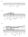
図1~図3を用いて、金属酸化物層と樹脂層とを分離する原理の一例を説明する。 An example of the principle of separating a metal oxide layer and a resin layer is explained using Figures 1 to 3.
まず、図1及び図2を用いて、H2Oが、金属酸化物層20と樹脂層23との密着性を阻
害する作用(以下、阻害作用)について説明する。
First, the action of H 2 O in inhibiting the adhesion between the
図1において、作製基板14上に金属酸化物層20が設けられ、金属酸化物層20上に樹
脂層23が設けられている。
In FIG. 1, a
金属酸化物層20と樹脂層23との界面、及び、金属酸化物層20中のうち一方または双
方には、H2O、水素(H)、酸素(O)、水酸基(OH)、水素ラジカル(H*)、酸
素ラジカル(O*)、ヒドロキシラジカル(OH*)のうち一つまたは複数が存在する。
これらは、金属酸化物層20の成膜工程、金属酸化物層20成膜後の添加(dope)工
程等によって供給することができる。図1のステップ(i)では、金属酸化物層20と樹
脂層23との界面、及び、金属酸化物層20中に、それぞれ、H2O、H、O等を有する
例を示す。
One or both of the interface between the
These can be supplied by a process for forming the
金属酸化物層20と樹脂層23との界面、及び、金属酸化物層20中に供給されたH、O
、H2Oなどは、樹脂層23(例えば、ポリイミド、アクリルなど)を固体化(固化、硬
化)させる工程(例えば、350℃での加熱)で当該界面にH2Oとして析出する場合が
ある。この場合、金属酸化物層20と樹脂層23との界面に析出したH2Oが、金属酸化
物層20と、樹脂層23との密着性を阻害する可能性がある。つまり、金属酸化物層20
と樹脂層23との界面に析出したH2Oは、密着性を阻害する作用(阻害作用)を有する
。図1のステップ(ii)では、金属酸化物層20中のH2Oが金属酸化物層20と樹脂
層23との界面に析出する例を示す。また、図1のステップ(ii)では、金属酸化物層
20中の水素と水酸基(OH)とが、金属酸化物層20と樹脂層23との界面にH2Oと
して析出する例を示す。
The interface between the
In some cases, H 2 O and the like may precipitate as H 2 O at the interface during the process of solidifying (hardening, curing) the resin layer 23 (e.g., polyimide, acrylic, etc.) (e.g., heating at 350° C.). In this case, the H 2 O precipitated at the interface between the
1 shows an example in which H 2 O in the
次に、作製基板14、金属酸化物層20、及び樹脂層23を有する積層体に光を照射する
。図2のステップ(iii)では、作製基板14が上側に位置する状態で積層体を配置す
る例を示す。図2のステップ(iii)では、搬送機構(図示しない)を用いて、図中の
矢印方向に積層体を移動させることで、図の右側から左側に向かって光が照射される。光
は、作製基板14を介して、金属酸化物層20と樹脂層23との界面またはその近傍に照
射される。ここでは、線状のレーザ光を用いる例を示す。図2のステップ(iii)、(
iv)では、線状ビーム26が、作製基板14を介して、加工領域27に照射される例を
示す。光照射により、金属酸化物層20と樹脂層23との界面(さらには金属酸化物層2
0中及び樹脂層23中)が加熱される。また、光照射により、金属酸化物層20と樹脂層
23との界面に存在するH2Oが、高エネルギーで瞬間的に気化(蒸発)してアブレーシ
ョンする(爆発する、ともいう)。
Next, light is irradiated onto the laminate having the
In iv), an example is shown in which the
In addition, the H 2 O present at the interface between the
図2のステップ(v)では、積層体の上下を反転する例を示す。図2のステップ(vi)
では、金属酸化物層20と樹脂層23とが分離されている例を示す。光照射により、H2
Oが水蒸気となり、体積が膨張する。これにより、金属酸化物層20と樹脂層23の密着
性が弱くなり、金属酸化物層20と樹脂層23の間を分離することができる。
Step (v) in FIG. 2 shows an example of inverting the stack.
In the example shown in FIG. 1 , the
The O turns into water vapor and expands in volume, which weakens the adhesion between the
次に、図3を用いて、金属酸化物層20と樹脂層23との間の結合について説明する。
Next, the bond between the
図3において、金属酸化物層20と樹脂層23とが積層されている。
In FIG. 3, a
金属酸化物層20と樹脂層23との間には、結合が生じていると考えられる。具体的には
共有結合、イオン結合、水素結合等の化学結合が、金属酸化物層20と樹脂層23との間
に生じている。
It is believed that a bond is formed between the
図3のステップ(i)では、金属酸化物層20が有する金属Mと、樹脂層23が有する炭
素Cとが、酸素Oによって結合されている例を示す。
Step (i) of FIG. 3 shows an example in which metal M contained in the
金属酸化物層20と樹脂層23の積層構造に光を照射する(図3のレーザ光55参照)。
ここでは、線状のレーザ光を用いる例を示す。基板と光源とを相対的に移動させることで
レーザ光55を走査し、分離したい領域に亘ってレーザ光55を照射する。
The laminated structure of the
Here, an example is shown in which a linear laser beam is used. The substrate and the light source are moved relatively to each other to scan the
光照射により、金属酸化物層20と樹脂層23との界面(さらには金属酸化物層20中及
び樹脂層23中)が加熱され、式(1)(下記及び図3参照)の反応が生じる。光を照射
することで、H2O(水蒸気)が、金属M-酸素O-炭素Cの結合を切断する。そして、
金属酸化物層20と樹脂層23との間の結合を、水素結合にする。
By the light irradiation, the interface between the
The bond between the
M-O-C+H2O→M-OH+C-OH・・・(1) M-O-C+H 2 O→M-OH+C-OH...(1)
図3のステップ(ii)では、金属酸化物層20が有する金属Mと酸素Oが結合し、樹脂
層23が有する炭素Cと別の酸素Oが結合している例を示す。2つの酸素は、それぞれ、
別の水素と共有結合を形成している。また、2つの酸素は、それぞれ、他方の酸素と結合
している水素と水素結合を形成している。
Step (ii) of Fig. 3 shows an example in which a metal M contained in the
It forms a covalent bond with another hydrogen, and each of the two oxygens forms a hydrogen bond with the hydrogen bonded to the other oxygen.
水素結合は、共有結合に比べて極めて弱い結合であるため、容易に切断することができる
。また、光照射のエネルギーにより、水は蒸発して水蒸気になる。このとき膨張する力に
よって、金属酸化物層20と樹脂層23の間の水素結合を切断することができる場合があ
る。したがって、金属酸化物層20と樹脂層23とを容易に分離することができる。
Hydrogen bonds are much weaker than covalent bonds and can be easily broken. Furthermore, water evaporates into steam due to the energy of light irradiation. The force of expansion at this time may be capable of breaking the hydrogen bonds between the
図3のステップ(iii)では、水素結合で結合されていた酸素と水素が離れ、金属酸化
物層20と樹脂層23とが分離されている例を示す。金属酸化物層20が有する金属Mと
酸素Oが結合し、樹脂層23が有する炭素Cと別の酸素Oが結合している。2つの酸素は
、それぞれ、別の水素と共有結合を形成している。
3, step (iii) shows an example in which oxygen and hydrogen bonded by hydrogen bonds are separated, and the
以上のように、金属酸化物層20と樹脂層23の積層構造に光を照射することで、H2O
が、金属酸化物層20と樹脂層23の間の強固な結合を、弱い結合である水素結合に変え
る。これにより、金属酸化物層20と樹脂層23の間の分離に要する力を低減させること
ができる。また、光照射のエネルギーにより、H2Oが膨張することで、金属酸化物層2
0と樹脂層23とを分離することができる。
As described above, by irradiating the laminated structure of the
However, the strong bond between the
0 and the
次に、上記阻害作用及び上記式(1)に示す反応に係るH2Oについて説明する。 Next, the above-mentioned inhibitory action and H 2 O involved in the reaction shown in the above formula (1) will be described.
H2Oは、金属酸化物層20中、樹脂層23中、及び金属酸化物層20と樹脂層23との
界面などに存在する場合がある。
H 2 O may be present in the
また、金属酸化物層20中、樹脂層23中、及び金属酸化物層20と樹脂層23との界面
などに存在していた水素(H)、酸素(O)、水酸基(OH)、水素ラジカル(H*)、
酸素ラジカル(O*)、ヒドロキシラジカル(OH*)等は、加熱されてH2Oとなる場
合がある。
In addition, hydrogen (H), oxygen (O), hydroxyl groups (OH), hydrogen radicals (H*), etc., which were present in the
Oxygen radicals (O * ), hydroxyl radicals (OH * ), and the like may become H2O when heated.
金属酸化物層20の内部、金属酸化物層20の表面(樹脂層23と接する面)、または金
属酸化物層20と樹脂層23の界面に、H2O、水素(H)、酸素(O)、水酸基(OH
)、水素ラジカル(H*)、酸素ラジカル(O*)、ヒドロキシラジカル(OH*)のう
ち一つまたは複数を添加することが好ましい。
The
It is preferable to add one or more of hydrogen radicals (H * ), oxygen radicals (O * ) and hydroxyl radicals (OH * ).
なお、本実施の形態の剥離方法では、上記の阻害作用と、先に示す式(1)の反応と、が
同時に生じる場合がある。この場合、金属酸化物層20と樹脂層23との密着性をさらに
低下させる、別言すると金属酸化物層20と樹脂層23との剥離性をさらに高めることが
できると推定される。
In the peeling method of the present embodiment, the above-mentioned inhibiting action and the reaction of formula (1) may occur simultaneously. In this case, it is presumed that the adhesion between the
金属酸化物層20中、樹脂層23中、及び金属酸化物層20と樹脂層23との界面などに
、H2O、水素(H)、酸素(O)、水酸基(OH)、水素ラジカル(H*)、酸素ラジ
カル(O*)、ヒドロキシラジカル(OH*)等を多く有することが好ましい。反応に寄
与するH2Oを多くすることで、反応を促進し、分離に要する力をより低減させることが
できる。
It is preferable that the
例えば、金属酸化物層20を形成する際に、金属酸化物層20中、または金属酸化物層2
0表面に、H2O、水素、酸素、水酸基、水素ラジカル(H*)、酸素ラジカル(O*)
、ヒドロキシラジカル(OH*)等を多く含ませることが好ましい。
For example, when forming the
On the surface, H 2 O, hydrogen, oxygen, hydroxyl group, hydrogen radical (H * ), oxygen radical (O * )
It is preferable that the water contains a large amount of hydroxyl radicals (OH * ).
具体的には、金属層を形成し、金属層の表面にラジカル処理を行うことで金属酸化物層2
0を形成することが好ましい。ラジカル処理では、酸素ラジカル及びヒドロキシラジカル
のうち少なくとも一方を含む雰囲気に、金属層の表面を曝すことが好ましい。例えば、酸
素または水蒸気(H2O)のうち一方または双方を含む雰囲気でプラズマ処理を行うこと
が好ましい。
Specifically, a metal layer is formed, and the surface of the metal layer is subjected to radical treatment to form a
In the radical treatment, it is preferable to expose the surface of the metal layer to an atmosphere containing at least one of oxygen radicals and hydroxyl radicals. For example, it is preferable to perform plasma treatment in an atmosphere containing one or both of oxygen and water vapor (H 2 O).
または、金属酸化物層20を形成し、金属酸化物層20の表面にラジカル処理を行うこと
が好ましい。ラジカル処理では、酸素ラジカル、水素ラジカル、及びヒドロキシラジカル
のうち少なくとも1種を含む雰囲気に、金属酸化物層20の表面を曝すことが好ましい。
例えば、酸素、水素、または水蒸気(H2O)のうち一つまたは複数を含む雰囲気でプラ
ズマ処理を行うことが好ましい。
Alternatively, it is preferable to form the
For example, it is preferable to perform the plasma treatment in an atmosphere containing one or more of oxygen, hydrogen, and water vapor (H 2 O).
ラジカル処理は、プラズマ発生装置またはオゾン発生装置を用いて行うことができる。 Radical treatment can be carried out using a plasma generator or an ozone generator.
例えば、酸素プラズマ処理、水素プラズマ処理、水プラズマ処理、オゾン処理等を行うこ
とができる。酸素プラズマ処理は、酸素を含む雰囲気下でプラズマを生成して行うことが
できる。水素プラズマ処理は、水素を含む雰囲気下でプラズマを生成して行うことができ
る。水プラズマ処理は、水蒸気(H2O)を含む雰囲気下でプラズマを生成して行うこと
ができる。特に水プラズマ処理を行うことで、金属酸化物層20の表面または内部に水分
を多く含ませることができ好ましい。
For example, oxygen plasma treatment, hydrogen plasma treatment, water plasma treatment, ozone treatment, etc. can be performed. The oxygen plasma treatment can be performed by generating plasma in an atmosphere containing oxygen. The hydrogen plasma treatment can be performed by generating plasma in an atmosphere containing hydrogen. The water plasma treatment can be performed by generating plasma in an atmosphere containing water vapor (H 2 O). In particular, the water plasma treatment is preferable because it allows the surface or interior of the
酸素、水素、水(水蒸気)、及び不活性ガス(代表的にはアルゴン)のうち2種以上を含
む雰囲気下でのプラズマ処理を行ってもよい。当該プラズマ処理としては、例えば、酸素
と水素とを含む雰囲気下でのプラズマ処理、酸素と水とを含む雰囲気下でのプラズマ処理
、水とアルゴンとを含む雰囲気下でのプラズマ処理、酸素とアルゴンとを含む雰囲気下で
のプラズマ処理、または酸素と水とアルゴンとを含む雰囲気下でのプラズマ処理などが挙
げられる。プラズマ処理のガスの一つとして、アルゴンガスを用いることで金属層または
金属酸化物層20にダメージを与えながら、プラズマ処理を行うことが可能となるため好
適である。
Plasma treatment may be performed in an atmosphere containing two or more of oxygen, hydrogen, water (water vapor), and an inert gas (typically argon). Examples of the plasma treatment include plasma treatment in an atmosphere containing oxygen and hydrogen, plasma treatment in an atmosphere containing oxygen and water, plasma treatment in an atmosphere containing water and argon, plasma treatment in an atmosphere containing oxygen and argon, or plasma treatment in an atmosphere containing oxygen, water, and argon. The use of argon gas as one of the gases for the plasma treatment is preferable because it allows the plasma treatment to be performed while damaging the metal layer or
2種以上のプラズマ処理を大気に暴露することなく連続で行ってもよい。例えば、アルゴ
ンプラズマ処理を行った後に、水プラズマ処理を行ってもよい。
Two or more types of plasma treatments may be performed consecutively without exposure to the atmosphere, for example, an argon plasma treatment may be performed followed by a water plasma treatment.
これにより、図4に示すように、金属酸化物層20の表面または内部に、水素、酸素、水
素ラジカル(H*)、酸素ラジカル(O*)、ヒドロキシラジカル(OH*)等を含ませ
ることができる。また、図4では、樹脂層23に、炭素Cと結合した水素H、水酸基OH
が含まれる例を示す。これらが、加熱処理や光照射により加熱され、H2Oとなることが
考えられる。
4, hydrogen, oxygen, hydrogen radicals (H * ), oxygen radicals (O * ), hydroxyl radicals (OH * ), etc. can be contained on or inside the
These may be heated by heat treatment or light irradiation to become H 2 O.
ランプ、レーザ装置等を用いて光を照射することができる。 Light can be emitted using a lamp, laser device, etc.
線状レーザ装置を用いてレーザ光を照射することが好ましい。低温ポリシリコン(LTP
S(Low Temperature Poly-Silicon))等の製造ラインの
レーザ装置を使用することができるため、これらの装置の有効利用が可能である。例えば
、LTPSの結晶化工程に用いる線状レーザ装置は、基板の向きを表裏逆にし、作製基板
14側を表面としてレーザ光を真上から照射することで、本発明の一態様におけるレーザ
光照射工程に、転用可能である。また、既存のLTPSの製造ラインは、酸化物半導体(
OS)を用いるトップゲート型のセルフアライン構造のトランジスタの製造ラインに適用
できる。このように、既存のLTPSの製造設備は、本発明の一態様の分離工程と、OS
トランジスタの製造工程を有する製造設備として容易に切り替え可能である。
It is preferable to irradiate the laser beam using a linear laser device.
Since the laser equipment of the manufacturing line of low temperature polysilicon (S) can be used, it is possible to effectively utilize these equipment. For example, the linear laser equipment used in the crystallization step of LTPS can be diverted to the laser light irradiation step in one embodiment of the present invention by turning the substrate upside down and irradiating the
The present invention can be applied to a manufacturing line for a top-gate self-aligned transistor using an OS.
It can be easily switched to a manufacturing facility having a transistor manufacturing process.
線状レーザは、矩形長尺状に集光(線状レーザビームに成形)して、金属酸化物層と樹脂
層との界面に光を照射する。
The linear laser is focused into a long rectangular shape (shaped into a linear laser beam), and the light is irradiated onto the interface between the metal oxide layer and the resin layer.
光は、波長領域が180nm以上450nm以下を有するように照射されることが好まし
い。光は、波長領域が308nm又はその近傍を有するように照射されることがより好ま
しい。
Preferably, the light is emitted to have a wavelength range of 180 nm to 450 nm, more preferably, the light is emitted to have a wavelength range of 308 nm or thereabouts.
本発明の一態様において、作製基板14、金属酸化物層20、及び樹脂層23の積層構造
の、レーザ光の吸収率は高いことが好ましい。例えば、当該積層構造における、波長30
8nmの光の吸収率は、80%以上100%以下であることが好ましく、85%以上10
0%以下であることが好ましい。レーザ光の大部分が当該積層構造で吸収されることで、
分離の歩留まりを高めることができる。また、機能素子にレーザ光が照射されることが抑
制され、機能素子の信頼性の低下を抑制できる。
In one embodiment of the present invention, it is preferable that the laminated structure of the
The absorptance of 8 nm light is preferably 80% or more and 100% or less, and more preferably 85% or more and 10
It is preferable that the absorption rate of the laser beam is 0% or less.
The separation yield can be increased. In addition, the functional element is prevented from being irradiated with the laser light, and the reliability of the functional element is prevented from being deteriorated.
光のエネルギー密度は、250mJ/cm2以上400mJ/cm2以下が好ましく、2
50mJ/cm2以上360mJ/cm2以下がより好ましい。
The energy density of the light is preferably 250 mJ/cm2 or more and 400 mJ/cm2 or less .
More preferably, the dose is 50 mJ/cm2 or more and 360 mJ/cm2 or less .
レーザ装置を用いて光を照射する場合、同一箇所に照射されるレーザ光のショット数は、
1ショット以上50ショット以下とすることができ、1ショットより多く10ショット以
下が好ましく、1ショットより多く5ショット以下がより好ましい。
When irradiating light using a laser device, the number of shots of laser light irradiated to the same location is:
The number of shots may be from 1 to 50, preferably from 1 to 10, and more preferably from 1 to 5.
ビームの短軸方向の両端には、光の強度が低い部分が存在する。そのため、当該光の強度
が低い部分の幅以上、一つのショットと次のショットの間にオーバーラップする部分を設
けることが好ましい。そのため、レーザ光のショット数は、1.1ショット以上とするこ
とが好ましく、1.25ショット以上とすることがより好ましい。
At both ends of the beam in the short axis direction, there are portions where the light intensity is low. Therefore, it is preferable to provide an overlap between one shot and the next shot that is equal to or greater than the width of the portion where the light intensity is low. Therefore, the number of shots of the laser light is preferably 1.1 shots or more, and more preferably 1.25 shots or more.
なお、本明細書中、レーザ光のショット数とは、ある点(領域)に照射されるレーザ光の
照射回数を指し、ビーム幅、スキャン速度、周波数、またはオーバーラップ率などで決定
される。また、線状のビームをあるスキャン方向に移動させているパルスとパルスの間、
即ち、一つのショットと次のショットの間にオーバーラップする部分があり、その重なる
比率がオーバーラップ率である。なお、オーバーラップ率が100%に近ければ近いほど
ショット数は多く、離れれば離れるほどショット数は少なくなり、スキャン速度が速けれ
ば速いほどショット数は少なくなる。
In this specification, the number of shots of laser light refers to the number of times that a point (area) is irradiated with laser light, and is determined by the beam width, scanning speed, frequency, overlap rate, etc. Also, the number of shots of laser light refers to the number of times that a linear beam is moved in a scanning direction between pulses.
In other words, there is an overlap between one shot and the next shot, and the ratio of the overlap is the overlap rate. Note that the closer the overlap rate is to 100%, the more shots there will be, and the further away the overlap rate is, the fewer shots there will be, and the faster the scan speed is, the fewer shots there will be.
上記のレーザ光のショット数が1.1ショットとは、連続する2つのショットの間にビー
ムの10分の1程度の幅のオーバーラップを有することを示し、オーバーラップ率10%
といえる。同様に、1.25ショットとは、連続する2つのショットの間にビームの4分
の1程度の幅のオーバーラップを有することを示し、オーバーラップ率25%といえる。
The number of laser beam shots of 1.1 indicates that there is an overlap of about 1/10 of the beam width between two consecutive shots, and the overlap rate is 10%.
Similarly, 1.25 shots indicates that there is an overlap between two successive shots with a width of about one-fourth of the beam, which is an overlap rate of 25%.
ここで、LTPSのレーザ結晶化の工程で照射する光のエネルギー密度は高く、例えば3
50mJ/cm2以上400mJ/cm2以下が挙げられる。また、レーザのショット数
も多く必要であり、例えば10ショット以上100ショット以下が挙げられる。
Here, the energy density of the light irradiated in the laser crystallization process of LTPS is high, for example, 3
The dose may be from 50 mJ/cm 2 to 400 mJ/cm 2. In addition, the number of laser shots is also required to be large, for example, from 10 shots to 100 shots.
一方、本実施の形態において、金属酸化物層20と樹脂層23とを分離するために行う光
の照射は、レーザ結晶化の工程で用いる条件よりも低いエネルギー密度、または少ないシ
ョット数で行うことができる。そのため、レーザ装置での処理可能な基板枚数を増やすこ
とができる。また、レーザ装置のメンテナンスの頻度の低減など、レーザ装置のランニン
グコストの低減が可能となる。したがって、表示装置などの作製コストを低減することが
できる。
On the other hand, in the present embodiment, the light irradiation for separating the
また、光の照射が、レーザ結晶化の工程で用いる条件よりも低いエネルギー密度、または
少ないショット数で行われることから、基板がレーザ光の照射により受けるダメージを低
減できる。そのため、基板を一度使用しても、強度が低下しにくく、基板を再利用できる
。したがって、コストを抑えることが可能となる。
In addition, the light irradiation is performed with a lower energy density or fewer shots than those used in the laser crystallization process, so damage to the substrate caused by the laser light irradiation can be reduced. Therefore, even if the substrate is used once, its strength is not easily reduced and it can be reused. This makes it possible to reduce costs.
また、本実施の形態では、作製基板14と樹脂層23との間に金属酸化物層20を配置す
る。金属酸化物層20を用いることで、金属酸化物層20を用いない場合に比べて、光の
照射を、低いエネルギー密度、または少ないショット数で行うことができることがある。
In the present embodiment, the
作製基板を介して光を照射する際、作製基板の光照射面にゴミなどの異物が付着している
と、光の照射ムラが生じ、剥離性が低い部分が形成され、金属酸化物層と樹脂層とを分離
する工程の歩留まりが低下することがある。そのため、光を照射する前、または光を照射
している間に、光照射面を洗浄することが好ましい。例えば、アセトンなどの有機溶剤、
水等を用いて作製基板の光照射面を洗浄することができる。また、エアナイフを用いて気
体を噴きつけながら光を照射してもよい。これにより、光の照射ムラを低減し、分離の歩
留まりを向上させることができる。
When light is irradiated through the substrate, if foreign matter such as dust is attached to the surface of the substrate to be irradiated with light, uneven light irradiation occurs, and parts with low peelability are formed, which may reduce the yield of the process of separating the metal oxide layer and the resin layer. Therefore, it is preferable to clean the surface to be irradiated with light before or during the light irradiation. For example, an organic solvent such as acetone,
The light irradiated surface of the substrate can be washed with water or the like. Alternatively, light may be irradiated while blowing gas using an air knife. This can reduce unevenness in light irradiation and improve the separation yield.
または、本実施の形態では、まず、基板上に金属酸化物層を形成する。次に、金属酸化物
層上に樹脂層を形成する。次に、基板上及び樹脂層上に、樹脂層の端部を覆う絶縁層を形
成する。次に、樹脂層上に、絶縁層を介して、チャネル形成領域に金属酸化物を有するト
ランジスタを形成する。次に、金属酸化物層と樹脂層との界面またはその近傍に光を照射
する。次に、樹脂層の少なくとも一部を金属酸化物層から分離することで、分離の起点を
形成する。そして、金属酸化物層と樹脂層とを分離する。
Alternatively, in this embodiment, first, a metal oxide layer is formed on a substrate. Next, a resin layer is formed on the metal oxide layer. Next, an insulating layer that covers an end of the resin layer is formed on the substrate and the resin layer. Next, a transistor having a metal oxide in a channel formation region is formed on the resin layer via the insulating layer. Next, light is irradiated to the interface between the metal oxide layer and the resin layer or its vicinity. Next, at least a part of the resin layer is separated from the metal oxide layer to form a starting point of separation. Then, the metal oxide layer and the resin layer are separated.
基板上には、樹脂層が接する部分と、絶縁層が接する部分と、が設けられる。絶縁層は、
樹脂層の端部を覆って設けられる。絶縁層は、樹脂層に比べて、金属酸化物層に対する密
着性もしくは接着性が高い。樹脂層の端部を覆って絶縁層を設けることで、光を照射した
後に、樹脂層が基板から意図せず剥がれることを抑制できる。例えば、レーザ装置から別
の場所に基板を搬送する時などに樹脂層が剥がれることを抑制できる。そして、分離の起
点を形成することで、所望のタイミングで、金属酸化物層と樹脂層とを分離することがで
きる。つまり、本実施の形態では、金属酸化物層と樹脂層の分離のタイミングを制御でき
、かつ、分離に要する力が小さい。これにより、金属酸化物層と樹脂層の分離工程、及び
表示装置の作製工程の歩留まりを高めることができる。
The substrate is provided with a portion that is in contact with the resin layer and a portion that is in contact with the insulating layer.
The insulating layer is provided to cover the end of the resin layer. The insulating layer has higher adhesion or bonding to the metal oxide layer than the resin layer. By providing the insulating layer to cover the end of the resin layer, it is possible to suppress the resin layer from being unintentionally peeled off from the substrate after irradiation with light. For example, it is possible to suppress the resin layer from being peeled off when the substrate is transported from the laser device to another location. Then, by forming a starting point of separation, the metal oxide layer and the resin layer can be separated at a desired timing. That is, in this embodiment, the timing of separation of the metal oxide layer and the resin layer can be controlled, and the force required for separation is small. This can increase the yield of the process of separating the metal oxide layer and the resin layer and the process of manufacturing the display device.
本実施の形態の表示装置は、トランジスタのチャネル形成領域に、金属酸化物を有するこ
とが好ましい。金属酸化物は、酸化物半導体として機能することができる。
The display device of this embodiment preferably includes a metal oxide in a channel formation region of a transistor, which can function as an oxide semiconductor.
トランジスタのチャネル形成領域に低温ポリシリコン(LTPS(Low Temper
ature Poly-Silicon))を用いる場合、500℃から550℃程度の
温度をかける必要があるため、樹脂層に耐熱性が求められる。また、レーザ結晶化の工程
でのダメージを緩和するため、樹脂層の厚膜化が必要となることがある。
Low Temperature Polysilicon (LTPS) is used in the channel formation region of the transistor.
When using a thick polysilicon (SiO2), the resin layer needs to be heat resistant because it needs to be heated to a temperature of about 500° C. to 550° C. Also, in order to mitigate damage during the laser crystallization process, it may be necessary to thicken the resin layer.
一方、チャネル形成領域に金属酸化物を用いたトランジスタは、350℃以下、さらには
300℃以下で形成することができる。そのため、樹脂層に高い耐熱性は求められない。
したがって、樹脂層の耐熱温度を低くすることができ、材料の選択の幅が広がる。
On the other hand, a transistor using a metal oxide for a channel formation region can be formed at 350° C. or less, or even 300° C. or less, so that the resin layer is not required to have high heat resistance.
Therefore, the heat resistance temperature of the resin layer can be lowered, and the range of materials to be selected is expanded.
また、チャネル形成領域に金属酸化物を用いたトランジスタは、レーザ結晶化の工程が不
要である。そして、本実施の形態では、レーザ結晶化の工程で用いる条件よりも、低いエ
ネルギー密度または少ないショット数で光を照射することができる。また、レーザ結晶化
の工程では、レーザ光が基板を介さずに樹脂層に照射されるが、本実施の形態では、作製
基板と金属酸化物層とを介して樹脂層に照射される。このように、樹脂層が受けるダメー
ジが少ないため、樹脂層の厚さを薄くすることができる。樹脂層に高耐熱性が要求されず
、薄膜化できることで、デバイス作製の大幅なコストダウンが期待できる。また、LTP
Sを用いる場合に比べて、工程が簡略化でき好ましい。
Moreover, a transistor using a metal oxide in the channel formation region does not require a laser crystallization process. In this embodiment, light can be irradiated with a lower energy density or a smaller number of shots than the conditions used in the laser crystallization process. In the laser crystallization process, the resin layer is irradiated with laser light without passing through a substrate, but in this embodiment, the resin layer is irradiated through the formation substrate and the metal oxide layer. In this way, the resin layer is less damaged, and the thickness of the resin layer can be made thin. Since the resin layer is not required to have high heat resistance and can be made thin, a significant cost reduction in device fabrication can be expected. In addition, LTP
This is preferable as it simplifies the process compared to the case where S is used.
ただし、本発明の一態様の表示装置は、トランジスタのチャネル形成領域に、金属酸化物
を有する構成に限定されない。例えば、本実施の形態の表示装置は、トランジスタのチャ
ネル形成領域に、シリコンを用いることができる。シリコンとしては、アモルファスシリ
コンまたは結晶性シリコンを用いることができる。結晶性シリコンとしては、微結晶シリ
コン、多結晶シリコン、単結晶シリコン等が挙げられる。
However, the display device of one embodiment of the present invention is not limited to a structure in which a channel formation region of a transistor includes a metal oxide. For example, in the display device of this embodiment, silicon can be used for the channel formation region of the transistor. As the silicon, amorphous silicon or crystalline silicon can be used. Examples of crystalline silicon include microcrystalline silicon, polycrystalline silicon, and single crystal silicon.
チャネル形成領域には、LTPSを用いることが好ましい。LTPSなどの多結晶シリコ
ンは、単結晶シリコンに比べて低温で形成でき、かつアモルファスシリコンに比べて高い
電界効果移動度と高い信頼性を備える。
It is preferable to use LTPS for the channel formation region. Polycrystalline silicon such as LTPS can be formed at a lower temperature than single crystal silicon, and has higher field effect mobility and higher reliability than amorphous silicon.
樹脂層23の厚さは、0.1μm以上5μm以下としてもよい。樹脂層23を薄く形成す
ることで、低コストで表示装置を作製できる。また、表示装置の軽量化及び薄型化が可能
となる。また、表示装置の可撓性を高めることができる。
The thickness of the
樹脂層23の可視光の透過性は特に限定されない。例えば、有色の層であってもよく、透
明の層であってもよい。ここで、表示装置の表示面側に樹脂層23が位置する場合、樹脂
層23が着色している(有色である)と、光取り出し効率が低下する、取り出される光の
色味が変わる、表示品位が低下する等の不具合が生じることがある。
The visible light transmittance of the
樹脂層23は、ウエットエッチング装置、ドライエッチング装置、アッシング装置等を用
いて除去することができる。特に、酸素プラズマを用いたアッシングを行って樹脂層23
を除去することが好適である。
The
It is preferable to remove
本実施の形態では、作製基板14と樹脂層23との間に金属酸化物層20を有する。金属
酸化物層20が光を吸収する機能を有するため、樹脂層23の光の吸収率が低くても、光
照射による効果が得られる。したがって、可視光の透過率が高い樹脂層23を用いること
ができる。そのため、表示装置の表示面側に樹脂層23が位置していても、高い表示品位
を実現できる。また、表示品位を高めるために、着色している(有色の)樹脂層23を除
去する工程を削減できる。また、樹脂層23の材料の選択の幅が広がる。
In this embodiment, the
樹脂層23の波長450nm以上700nm以下の範囲の光の透過率の平均値は、70%
以上100%以下が好ましく、80%以上100%以下が好ましく、90%以上100%
以下がより好ましい。
The average transmittance of the
Preferably, 80% or more and 100% or less, more preferably, 90% or more and 100% or less.
The following is more preferred:
本実施の形態では、樹脂層の耐熱温度以下の温度で、トランジスタ等を形成する。樹脂層
の耐熱性は、例えば、加熱による重量減少率、具体的には5%重量減少温度等で評価でき
る。本実施の形態の剥離方法及び表示装置の作製方法では、工程中の最高温度を低くする
ことができる。例えば、本実施の形態では、樹脂層の5%重量減少温度を、200℃以上
650℃以下、200℃以上500℃以下、200℃以上400℃以下、または200℃
以上350℃以下とすることができる。そのため、材料の選択の幅が広がる。なお、樹脂
層の5%重量減少温度は、650℃より高くてもよい。
In this embodiment, a transistor or the like is formed at a temperature equal to or lower than the heat resistance temperature of the resin layer. The heat resistance of the resin layer can be evaluated, for example, by the weight loss rate due to heating, specifically, the 5% weight loss temperature. In the peeling method and the manufacturing method of the display device of this embodiment, the maximum temperature during the process can be lowered. For example, in this embodiment, the 5% weight loss temperature of the resin layer can be set to 200° C. or higher and 650° C. or lower, 200° C. or higher and 500° C. or lower, 200° C. or higher and 400° C. or lower, or 200° C. or higher.
The 5% weight loss temperature of the resin layer may be higher than 650° C., and the range of materials to be selected may be wider.
分離前または分離中に、分離界面に水を含む液体を供給することが好ましい。分離界面に
水が存在することで、樹脂層23と金属酸化物層20との密着性もしくは接着性をより低
下させ、分離に要する力を低減させることができる。また、分離界面に水を含む液体を供
給することで、樹脂層23と金属酸化物層20との間の結合を弱めるもしくは切断する効
果を奏することがある。液体との化学結合を利用して、樹脂層23と金属酸化物層20の
間の結合を切って分離を進行させることができる。例えば、樹脂層23と金属酸化物層2
0との間に水素結合が形成されている場合、水を含む液体が供給されることで、水と、樹
脂層23または金属酸化物層20との間に水素結合が形成され、樹脂層23と金属酸化物
層20との間の水素結合が切れることが考えられる。
It is preferable to supply a liquid containing water to the separation interface before or during separation. The presence of water at the separation interface can further reduce the adhesion or bonding between the
0, it is conceivable that when a liquid containing water is supplied, hydrogen bonds will be formed between the water and the
金属酸化物層20は、表面張力が小さく、水を含む液体に対する濡れ性が高いことが好ま
しい。これにより、金属酸化物層20の表面全体に水を含む液体を行き渡らせ、分離界面
に水を含む液体を容易に供給できる。金属酸化物層20全体に水が広がることで、均一な
剥離ができる。
It is preferable that the
金属酸化物層20の水を含む液体との接触角は、0°より大きく60°以下が好ましく、
0°より大きく50°以下がより好ましい。なお、水を含む液体に対する濡れ性が極めて
高い場合(例えば接触角が約20°以下の場合)には、接触角の正確な値の取得が困難な
ことがある。金属酸化物層20は、水を含む液体に対する濡れ性が高いほど好適であるた
め、上記接触角の正確な値が取得できないほど、水を含む液体に対する濡れ性が高くても
よい。
The contact angle of the
More preferably, the contact angle is greater than 0° and equal to or less than 50°. When the wettability to liquids including water is extremely high (for example, when the contact angle is equal to or less than about 20°), it may be difficult to obtain an accurate value of the contact angle. Since the
分離界面に水を含む液体が存在することで、分離時に生じる静電気が、被剥離層に含まれ
る機能素子に悪影響を及ぼすこと(半導体素子が静電気により破壊されるなど)を抑制で
きる。また、イオナイザなどを用いて、分離により露出した被剥離層の表面を除電しても
よい。
The presence of a liquid containing water at the separation interface can prevent static electricity generated during separation from adversely affecting the functional elements contained in the peeled layer (e.g., semiconductor elements being destroyed by static electricity). In addition, an ionizer or the like may be used to neutralize the surface of the peeled layer exposed by separation.
分離界面に液体を供給した場合は、分離により露出した被剥離層の表面を乾燥してもよい
。
When a liquid is supplied to the separation interface, the surface of the layer to be peeled off that is exposed by the separation may be dried.
以下では、本実施の形態の表示装置の作製方法について、具体的に説明する。 The method for manufacturing the display device of this embodiment will be described in detail below.
なお、表示装置を構成する薄膜(絶縁膜、半導体膜、導電膜等)は、スパッタリング法、
化学気相堆積(CVD:Chemical Vapor Deposition)法、真
空蒸着法、パルスレーザ堆積(PLD:Pulsed Laser Depositio
n)法、原子層成膜(ALD:Atomic Layer Deposition)法等
を用いて形成することができる。CVD法としては、プラズマ化学気相堆積(PECVD
:Plasma Enhanced Chemical Vapor Depositi
on)法や、熱CVD法でもよい。熱CVD法の例として、有機金属化学気相堆積(MO
CVD:Metal Organic CVD)法を使ってもよい。
The thin films (insulating films, semiconductor films, conductive films, etc.) constituting the display device are formed by sputtering,
Chemical Vapor Deposition (CVD), Vacuum Deposition, Pulsed Laser Deposition (PLD)
The CVD method may be a plasma enhanced chemical vapor deposition (PECVD) method, an atomic layer deposition (ALD) method, or the like.
:Plasma Enhanced Chemical Vapor Deposit
The thermal CVD method may be a metal-organic chemical vapor deposition (MOCVD) method.
A CVD (Metal Organic CVD) method may also be used.
表示装置を構成する薄膜(絶縁膜、半導体膜、導電膜等)は、スピンコート、ディップ、
スプレー塗布、インクジェット、ディスペンス、スクリーン印刷、オフセット印刷、ドク
ターナイフ、スリットコート、ロールコート、カーテンコート、ナイフコート等の方法に
より形成することができる。
Thin films (insulating films, semiconductor films, conductive films, etc.) that make up the display device are formed by spin coating, dipping,
The coating can be performed by a method such as spray coating, ink jet, dispensing, screen printing, offset printing, doctor knife, slit coating, roll coating, curtain coating, knife coating, or the like.
表示装置を構成する薄膜を加工する際には、リソグラフィ法等を用いて加工することがで
きる。または、シャドウマスクを用いた成膜方法により、島状の薄膜を形成してもよい。
または、ナノインプリント法、サンドブラスト法、リフトオフ法などにより薄膜を加工し
てもよい。フォトリソグラフィ法としては、加工したい薄膜上にレジストマスクを形成し
て、エッチング等により当該薄膜を加工し、レジストマスクを除去する方法と、感光性を
有する薄膜を成膜した後に、露光、現像を行って、当該薄膜を所望の形状に加工する方法
と、がある。
When processing the thin film constituting the display device, it is possible to process it using a lithography method, etc. Alternatively, an island-shaped thin film may be formed by a film forming method using a shadow mask.
Alternatively, the thin film may be processed by a nanoimprint method, a sandblasting method, a lift-off method, etc. Photolithography includes a method in which a resist mask is formed on the thin film to be processed, the thin film is processed by etching or the like, and the resist mask is removed, and a method in which a photosensitive thin film is formed, and then exposed and developed to process the thin film into a desired shape.
リソグラフィ法において光を用いる場合、露光に用いる光は、例えばi線(波長365n
m)、g線(波長436nm)、h線(波長405nm)、またはこれらを混合させた光
を用いることができる。そのほか、紫外線やKrFレーザ光、またはArFレーザ光等を
用いることもできる。また、液浸露光技術により露光を行ってもよい。また、露光に用い
る光として、極端紫外光(EUV:Extreme Ultra-violet)やX線
を用いてもよい。また、露光に用いる光に換えて、電子ビームを用いることもできる。極
端紫外光、X線または電子ビームを用いると、極めて微細な加工が可能となるため好まし
い。なお、電子ビームなどのビームを走査することにより露光を行う場合には、フォトマ
スクは不要である。
When light is used in the lithography method, the light used for exposure is, for example, i-line (
m rays (wavelength 436 nm), g rays (wavelength 405 nm), or a mixture of these rays can be used. In addition, ultraviolet light, KrF laser light, ArF laser light, or the like can be used. Exposure may be performed by immersion exposure technology. Extreme ultraviolet light (EUV: Extreme Ultra-violet) or X-rays may be used as the light used for exposure. An electron beam may be used instead of the light used for exposure. Extreme ultraviolet light, X-rays, or an electron beam are preferable because they enable extremely fine processing. When exposure is performed by scanning a beam such as an electron beam, a photomask is not required.
薄膜のエッチングには、ドライエッチング法、ウエットエッチング法、サンドブラスト法
などを用いることができる。
For etching the thin film, a dry etching method, a wet etching method, a sandblasting method, or the like can be used.
[剥離方法]
まず、作製基板14上に、金属酸化物層20を形成する(図5(A1))。または、作製
基板14上に、金属層19と金属酸化物層20とを積層する(図5(A2))。
[Removal method]
First, a
作製基板14は、搬送が容易となる程度に剛性を有し、かつ作製工程にかかる温度に対し
て耐熱性を有する。作製基板14に用いることができる材料としては、例えば、ガラス、
石英、セラミック、サファイヤ、樹脂、半導体、金属または合金などが挙げられる。ガラ
スとしては、例えば、無アルカリガラス、バリウムホウケイ酸ガラス、アルミノホウケイ
酸ガラス等が挙げられる。
The
Examples of the glass include quartz, ceramic, sapphire, resin, semiconductor, metal or alloy, etc. Examples of the glass include alkali-free glass, barium borosilicate glass, aluminoborosilicate glass, etc.
上述の通り、本実施の形態では、作製基板14と樹脂層23の間に下地層を形成する。下
地層は、樹脂層23との密着性(接着性)が、作製基板14よりも低い層である。本実施
の形態では、金属酸化物層20を用いる場合を例に挙げて説明するが、これに限られない
。
As described above, in the present embodiment, a base layer is formed between the
具体的には、下地層には、チタン、モリブデン、アルミニウム、タングステン、シリコン
、インジウム、亜鉛、ガリウム、タンタル、錫、ハフニウム、イットリウム、ジルコニウ
ム、マグネシウム、ランタン、セリウム、ネオジム、ビスマス、及びニオブのうち一つま
たは複数を有する層を用いることができる。下地層には、金属、合金、及びそれらの化合
物(金属酸化物など)を含むことができる。下地層は、チタン、モリブデン、アルミニウ
ム、タングステン、シリコン、インジウム、亜鉛、ガリウム、タンタル、及び錫のうち一
つまたは複数を有することが好ましい。
Specifically, the underlayer may be a layer containing one or more of titanium, molybdenum, aluminum, tungsten, silicon, indium, zinc, gallium, tantalum, tin, hafnium, yttrium, zirconium, magnesium, lanthanum, cerium, neodymium, bismuth, and niobium. The underlayer may contain a metal, an alloy, or a compound thereof (such as a metal oxide). The underlayer preferably contains one or more of titanium, molybdenum, aluminum, tungsten, silicon, indium, zinc, gallium, tantalum, and tin.
また、下地層の材料は、無機材料に限られず、有機材料を用いてもよい。例えば、有機E
L素子のEL層に用いることができる各種有機材料を用いてもよい。下地層として、これ
ら有機材料の蒸着膜を用いることができる。これにより、密着性の低い膜を形成できる。
The material of the underlayer is not limited to inorganic materials, but may be organic materials. For example, organic E
Various organic materials that can be used for the EL layer of the L element may be used. As the underlayer, a vapor deposition film of such an organic material can be used. This allows the formation of a film with low adhesion.
金属層19には、各種金属や合金等を用いることができる。
Various metals, alloys, etc. can be used for the
金属酸化物層20には、各種金属の酸化物を用いることができる。金属酸化物としては、
例えば、酸化チタン(TiOx)、酸化モリブデン、酸化アルミニウム、酸化タングステ
ン、シリコンを含むインジウム錫酸化物(ITSO)、インジウム亜鉛酸化物、In-G
a-Zn酸化物等が挙げられる。
The
For example, titanium oxide (TiO x ), molybdenum oxide, aluminum oxide, tungsten oxide, indium tin oxide containing silicon (ITSO), indium zinc oxide, In-G
Examples include a-Zn oxide.
そのほか、金属酸化物としては、酸化インジウム、チタンを含むインジウム酸化物、タン
グステンを含むインジウム酸化物、インジウム錫酸化物(ITO)、チタンを含むITO
、タングステンを含むインジウム亜鉛酸化物、酸化亜鉛(ZnO)、ガリウムを含むZn
O、酸化ハフニウム、酸化イットリウム、酸化ジルコニウム、酸化ガリウム、酸化タンタ
ル、酸化マグネシウム、酸化ランタン、酸化セリウム、酸化ネオジム、酸化スズ、酸化ビ
スマス、チタン酸塩、タンタル酸塩、ニオブ酸塩等が挙げられる。
Other examples of metal oxides include indium oxide, indium oxide containing titanium, indium oxide containing tungsten, indium tin oxide (ITO), and ITO containing titanium.
, Indium zinc oxide containing tungsten, zinc oxide (ZnO), Zn containing gallium
Examples of oxides that can be used include O, hafnium oxide, yttrium oxide, zirconium oxide, gallium oxide, tantalum oxide, magnesium oxide, lanthanum oxide, cerium oxide, neodymium oxide, tin oxide, bismuth oxide, titanates, tantalates, and niobates.
金属酸化物層20の形成方法に特に限定は無い。例えば、スパッタリング法、プラズマC
VD法、蒸着法、ゾルゲル法、電気泳動法、スプレー法等を用いて形成することができる
。
There is no particular limitation on the method for forming the
It can be formed by using a VD method, a vapor deposition method, a sol-gel method, an electrophoresis method, a spray method, or the like.
金属層を成膜した後に、当該金属層に酸素を導入することで、金属酸化物層20を形成す
ることができる。このとき、金属層の表面のみ、または金属層全体を酸化させる。前者の
場合、金属層に酸素を導入することで、金属層19と金属酸化物層20との積層構造が形
成される(図5(A2))。
After forming a metal layer, oxygen is introduced into the metal layer to form a
例えば、酸素を含む雰囲気下で金属層を加熱することで、金属層を酸化させることができ
る。酸素を含むガスを流しながら金属層を加熱することが好ましい。金属層を加熱する温
度は、100℃以上500℃以下が好ましく、100℃以上450℃以下がより好ましく
、100℃以上400℃以下がより好ましく、100℃以上350℃以下がさらに好まし
い。
For example, the metal layer can be oxidized by heating the metal layer in an atmosphere containing oxygen. It is preferable to heat the metal layer while flowing a gas containing oxygen. The temperature at which the metal layer is heated is preferably 100° C. or more and 500° C. or less, more preferably 100° C. or more and 450° C. or less, more preferably 100° C. or more and 400° C. or less, and even more preferably 100° C. or more and 350° C. or less.
金属層は、トランジスタの作製における最高温度以下の温度で加熱されることが好ましい
。これにより、表示装置の作製における最高温度が高くなることを防止できる。トランジ
スタの作製における最高温度以下とすることで、トランジスタの作製工程における製造装
置などを流用することが可能となるため、追加の設備投資などを抑制することができる。
したがって、生産コストが抑制された表示装置とすることができる。例えば、トランジス
タの作製温度が350℃までである場合、加熱処理の温度は350℃以下とすることが好
ましい。
The metal layer is preferably heated at a temperature equal to or lower than the maximum temperature in the manufacture of the transistor. This can prevent the maximum temperature in the manufacture of the display device from becoming too high. By setting the temperature at or lower than the maximum temperature in the manufacture of the transistor, it is possible to reuse manufacturing equipment and the like in the manufacture of the transistor, and therefore additional capital investment and the like can be suppressed.
Therefore, a display device can be manufactured at reduced costs.For example, when the manufacturing temperature of a transistor is up to 350° C., the heat treatment temperature is preferably 350° C. or less.
または、金属層の表面にラジカル処理を行うことで金属層を酸化させることができる。ラ
ジカル処理では、酸素ラジカル及びヒドロキシラジカルのうち少なくとも一方を含む雰囲
気に、金属層の表面を曝すことが好ましい。例えば、酸素または水蒸気(H2O)のうち
一方または双方を含む雰囲気でプラズマ処理を行うことが好ましい。
Alternatively, the metal layer can be oxidized by performing radical treatment on the surface of the metal layer. In the radical treatment, it is preferable to expose the surface of the metal layer to an atmosphere containing at least one of oxygen radicals and hydroxyl radicals. For example, it is preferable to perform plasma treatment in an atmosphere containing one or both of oxygen and water vapor (H 2 O).
上述の通り、金属酸化物層20の表面または内部に、水素、酸素、水素ラジカル(H*)
、酸素ラジカル(O*)、ヒドロキシラジカル(OH*)等を含ませることで、金属酸化
物層20と樹脂層23との分離に要する力を低減できる。このことからも、金属酸化物層
20の形成に、ラジカル処理もしくはプラズマ処理を行うことは好適である。
As described above, hydrogen, oxygen, hydrogen radicals (H * ) are present on the surface or inside of the
By including radicals (O * ), hydroxyl radicals (OH * ), etc., it is possible to reduce the force required to separate the
金属層の表面にラジカル処理もしくはプラズマ処理を行うことで金属層を酸化させる場合
、金属層を高温で加熱する工程が不要となる。そのため、表示装置の作製における最高温
度が高くなることを防止できる。
When the surface of the metal layer is subjected to radical treatment or plasma treatment to oxidize the metal layer, a step of heating the metal layer at a high temperature becomes unnecessary, so that the maximum temperature during the manufacture of the display device can be prevented from becoming high.
または、酸素雰囲気下で、金属酸化物層20を形成することができる。例えば、酸素を含
むガスを流しながら、スパッタリング法を用いて金属酸化物膜を成膜することで、金属酸
化物層20を形成できる。この場合も、金属酸化物層20の表面にラジカル処理を行うこ
とが好ましい。ラジカル処理では、酸素ラジカル、水素ラジカル、及びヒドロキシラジカ
ルのうち少なくとも1種を含む雰囲気に、金属酸化物層20の表面を曝すことが好ましい
。例えば、酸素、水素、または水蒸気(H2O)のうち一つまたは複数を含む雰囲気でプ
ラズマ処理を行うことが好ましい。
Alternatively, the
ラジカル処理の詳細については、先に記した内容を参照できる。 For more details on radical processing, please refer to the above.
そのほか、酸素、水素、水等の導入方法としては、イオン注入法、イオンドーピング法、
プラズマイマージョンイオン注入法等を用いることができる。
Other methods for introducing oxygen, hydrogen, water, etc. include ion implantation, ion doping,
A plasma immersion ion implantation method or the like can be used.
金属層19の厚さは、1nm以上100nm以下が好ましく、1nm以上50nm以下が
より好ましく、1nm以上20nm以下がより好ましい。
The thickness of the
金属酸化物層20の厚さは、例えば、1nm以上200nm以下が好ましく、5nm以上
100nm以下がより好ましく、5nm以上50nm以下がより好ましい。なお、金属層
を用いて金属酸化物層20を形成する場合、最終的に形成される金属酸化物層20の厚さ
は、成膜した金属層の厚さよりも厚くなることがある。
The thickness of the
分離前または分離中に、金属酸化物層20と樹脂層23との界面に水を含む液体を供給す
ることで、分離に要する力を低減させることができる。金属酸化物層20と当該液体との
接触角が小さいほど、液体供給による効果を高めることができる。具体的には、金属酸化
物層20の水を含む液体との接触角は、0°より大きく60°以下が好ましく、0°より
大きく50°以下がより好ましい。
By supplying a liquid containing water to the interface between the
金属酸化物層20には、酸化チタン、酸化タングステン等が好適である。酸化チタンを用
いると、酸化タングステンよりもコストを低減でき、好ましい。
Titanium oxide, tungsten oxide, etc. are suitable for the
金属酸化物層20は光触媒機能を有してもよい。光触媒機能を有する金属酸化物層に光を
照射することで、光触媒反応を生じさせることができる。これにより、金属酸化物層と樹
脂層との結合力を弱め、容易に分離できる場合がある。金属酸化物層20には、金属酸化
物層20を活性化させる波長の光を適宜照射することができる。例えば、金属酸化物層2
0に紫外光を照射する。例えば、金属酸化物層20の成膜後、他の層を介することなく、
金属酸化物層20に直接、紫外光を照射してもよい。紫外光の照射には、紫外光ランプを
好適に用いることができる。紫外光ランプとしては、水銀ランプ、水銀キセノンランプ、
メタルハライドランプ等が挙げられる。または、分離前に行うレーザ照射工程によって、
金属酸化物層20を活性化させてもよい。
The
For example, after the
The
Metal halide lamps, etc. Alternatively, a laser irradiation step performed before separation can be used to
The
金属もしくは窒素を添加した酸化チタンを用いてもよい。これらの元素を添加した酸化チ
タンを用いて金属酸化物層20を形成すると、紫外光でなく、可視光によって活性化させ
ることができる。
Titanium oxide doped with a metal or nitrogen may also be used. When the
次に、金属酸化物層20上に、第1の層24を形成する(図5(B))。
Next, a
図5(B)では塗布法を用いて金属酸化物層20の一面全体に第1の層24を形成する例
を示す。これに限られず、印刷法等を用いて第1の層24を形成してもよい。金属酸化物
層20上に、島状の第1の層24、開口または凹凸形状を有する第1の層24等を形成し
てもよい。
5B shows an example in which the
第1の層24は、各種樹脂材料(樹脂前駆体を含む)を用いて形成することができる。
The
第1の層24は、熱硬化性を有する材料を用いて形成することが好ましい。
The
第1の層24は、感光性を有する材料を用いて形成してもよく、感光性を有さない材料(
非感光性の材料ともいう)を用いて形成してもよい。
The
The insulating layer 11 may be formed using a non-photosensitive material.
感光性を有する材料を用いると、光を用いたリソグラフィ法により、第1の層24の一部
を除去し、所望の形状の樹脂層23を形成することができる。
If a photosensitive material is used, a part of the
第1の層24は、ポリイミド樹脂、ポリイミド樹脂前駆体、またはアクリル樹脂を含む材
料を用いて形成されることが好ましい。第1の層24は、例えば、ポリイミド樹脂と溶媒
を含む材料、ポリアミック酸と溶媒を含む材料、またはアクリル樹脂と溶媒を含む材料等
を用いて形成できる。なお、第1の層24として、ポリイミド樹脂またはポリイミド樹脂
前駆体を含む材料を用いると、比較的耐熱性を高められるため好適である。一方で、第1
の層24として、アクリル樹脂を含む材料を用いると、可視光における透光性を高められ
るため好適である。ポリイミド樹脂及びアクリル樹脂は、それぞれ、表示装置の平坦化膜
等に好適に用いられる材料であるため、成膜装置や材料を共有することができる。そのた
め本発明の一態様の構成を実現するために新たな装置や材料を必要としない。このように
、第1の層24は、特別な材料は必要でなく、表示装置に用いる樹脂材料を用いて形成で
きるため、コストを削減することができる。
The
The use of a material containing an acrylic resin as the
具体的には、樹脂層23は、構造式(100)で表される化合物(オキシジフタル酸)の
残基を有することが好ましい。
Specifically, the
樹脂層23には、オキシジフタル酸またはオキシジフタル酸誘導体を含む酸成分と、芳香
族アミンまたは芳香族アミン誘導体を含むアミン成分と、を用いて得られるポリイミド樹
脂が好適である。オキシジフタル酸誘導体としては、例えば、オキシジフタル酸無水物が
挙げられる。また、樹脂層23は、フッ素を含んでいてもよい。樹脂層23中にフッ素を
含む場合、当該フッ素を用いて、金属酸化物層20と樹脂層23の間の水素結合が形成さ
れることがある。
The
また、第1の層24に好適に用いることができる、ポリイミド樹脂またはポリイミド樹脂
前駆体を含む材料の物性値について、表1に示す。
Table 1 shows the physical properties of materials containing polyimide resin or polyimide resin precursors that can be suitably used for the
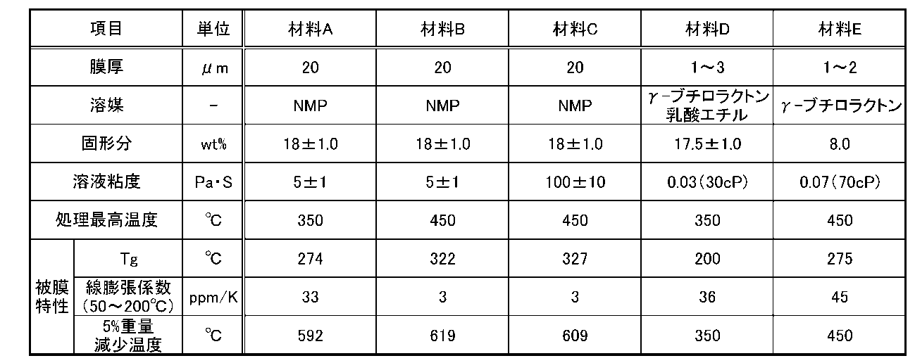
表1に示す材料A~材料Eを用いて樹脂層23を形成することができる。樹脂層23の信
頼性を高めることができるため、材料のガラス転移温度(Tg)及び5%重量減少温度は
、それぞれ高い方が好ましい。
The
そのほか、第1の層24の形成に用いることができる樹脂材料としては、例えば、エポキ
シ樹脂、ポリアミド樹脂、ポリイミドアミド樹脂、シロキサン樹脂、ベンゾシクロブテン
系樹脂、フェノール樹脂、及びこれら樹脂の前駆体等が挙げられる。
Other examples of resin materials that can be used to form the
第1の層24は、スピンコータを用いて形成することが好ましい。スピンコート法を用い
ることで、大判基板に薄い膜を均一に形成することができる。
The
第1の層24は、粘度が5cP以上500cP未満、好ましくは5cP以上100cP未
満、より好ましくは10cP以上50cP以下の溶液を用いて形成することが好ましい。
溶液の粘度が低いほど、塗布が容易となる。また、溶液の粘度が低いほど、気泡の混入を
抑制でき、良質な膜を形成できる。
The
The lower the viscosity of the solution, the easier it is to apply the solution. Also, the lower the viscosity of the solution, the more likely it is that air bubbles will be prevented from being mixed in, and the better the quality of the film that can be formed.
そのほか、第1の層24の形成方法としては、ディップ、スプレー塗布、インクジェット
、ディスペンス、スクリーン印刷、オフセット印刷、ドクターナイフ、スリットコート、
ロールコート、カーテンコート、ナイフコート等が挙げられる。
Other methods for forming the
Examples include roll coating, curtain coating, and knife coating.
次に、第1の層24に対して加熱処理を行うことで、樹脂層23を形成する(図5(C)
)。
Next, the
).
加熱処理は、例えば、加熱装置のチャンバーの内部に、酸素、窒素、及び希ガス(アルゴ
ンなど)のうち一つまたは複数を含むガスを流しながら行うことができる。または、加熱
処理は、大気雰囲気下で加熱装置のチャンバー、ホットプレート等を用いて行うことがで
きる。
The heat treatment can be performed, for example, while a gas containing one or more of oxygen, nitrogen, and a rare gas (such as argon) is flowing inside a chamber of a heating device, or the heat treatment can be performed in an air atmosphere using a chamber, a hot plate, or the like of a heating device.
大気雰囲気下や酸素を含むガスを流しながら加熱を行うと、樹脂層23が酸化により着色
し、可視光に対する透過性が低下することがある。
If the heating is performed in an air atmosphere or while a gas containing oxygen is being flowed, the
そのため、窒素ガスを流しながら、加熱を行うことが好ましい。これにより、加熱雰囲気
中に含まれる酸素を大気雰囲気よりも少なくすることができ、樹脂層23の酸化を抑制し
、樹脂層23の可視光に対する透過性を高めることができる。
For this reason, it is preferable to perform heating while flowing nitrogen gas, which can reduce the amount of oxygen contained in the heating atmosphere compared to the air atmosphere, suppress oxidation of the
加熱処理により、樹脂層23中の脱ガス成分(例えば、水素、水等)を低減することがで
きる。特に、樹脂層23上に形成する各層の作製温度以上の温度で加熱することが好まし
い。これにより、トランジスタの作製工程における、樹脂層23からの脱ガスを大幅に抑
制することができる。
The heat treatment can reduce degassed components (e.g., hydrogen, water, etc.) in the
例えば、トランジスタの作製温度が350℃までである場合、樹脂層23となる膜を35
0℃以上450℃以下で加熱することが好ましく、400℃以下がより好ましく、375
℃以下がさらに好ましい。これにより、トランジスタの作製工程における、樹脂層23か
らの脱ガスを大幅に抑制することができる。
For example, when the manufacturing temperature of the transistor is up to 350° C., the film to be the
Heating is preferably performed at 0° C. or higher and 450° C. or lower, more preferably 400° C. or lower, and more preferably 375° C. or lower.
C. or less, more preferably. This makes it possible to significantly suppress degassing from the
加熱処理の温度は、トランジスタの作製における最高温度以下の温度とすることが好まし
い。トランジスタの作製における最高温度以下とすることで、トランジスタの作製工程に
おける製造装置などを流用することが可能となるため、追加の設備投資などを抑制するこ
とができる。したがって、生産コストが抑制された表示装置とすることができる。例えば
、トランジスタの作製温度が350℃までである場合、加熱処理の温度は350℃以下と
することが好ましい。
The temperature of the heat treatment is preferably set to a temperature equal to or lower than the maximum temperature in the manufacture of the transistor. By setting the temperature to be equal to or lower than the maximum temperature in the manufacture of the transistor, it is possible to reuse manufacturing equipment and the like in the manufacturing process of the transistor, and therefore additional capital investment and the like can be suppressed. Therefore, a display device with reduced production costs can be obtained. For example, when the manufacturing temperature of the transistor is up to 350° C., the temperature of the heat treatment is preferably set to be equal to or lower than 350° C.
トランジスタの作製における最高温度と、加熱処理の温度を等しくすると、加熱処理を行
うことで表示装置の作製における最高温度が高くなることを防止でき、かつ樹脂層23の
脱ガス成分を低減できるため、好ましい。
It is preferable to set the maximum temperature in the manufacture of the transistor and the temperature of the heat treatment to be equal to each other, because the maximum temperature in the manufacture of the display device can be prevented from becoming high by the heat treatment and degassing components of the
処理時間を長くすることで、加熱温度が比較的低い場合であっても、加熱温度がより高い
条件の場合と同等の剥離性を実現できる場合がある。そのため、加熱装置の構成により加
熱温度を高められない場合には、処理時間を長くすることが好ましい。
By increasing the treatment time, even if the heating temperature is relatively low, it may be possible to achieve peelability equivalent to that achieved when the heating temperature is higher. Therefore, when the heating temperature cannot be increased due to the configuration of the heating device, it is preferable to increase the treatment time.
加熱処理の時間は、例えば、5分以上24時間以下が好ましく、30分以上12時間以下
がより好ましく、1時間以上6時間以下がさらに好ましい。なお、加熱処理の時間はこれ
に限定されない。例えば、加熱処理を、RTA(Rapid Thermal Anne
aling)法を用いて行う場合などは、5分未満としてもよい。
The time for the heat treatment is, for example, preferably 5 minutes to 24 hours, more preferably 30 minutes to 12 hours, and even more preferably 1 hour to 6 hours. The time for the heat treatment is not limited thereto. For example, the heat treatment may be performed by RTA (Rapid Thermal Annex).
In some cases, such as when the ion implantation is performed using the ion implantation method, the time may be less than 5 minutes.
加熱装置としては、電気炉や、抵抗発熱体などの発熱体からの熱伝導または熱輻射によっ
て被処理物を加熱する装置等、様々な装置を用いることができる。例えば、GRTA(G
as Rapid Thermal Anneal)装置、LRTA(Lamp Rap
id Thermal Anneal)装置等のRTA装置を用いることができる。LR
TA装置は、ハロゲンランプ、メタルハライドランプ、キセノンアークランプ、カーボン
アークランプ、高圧ナトリウムランプ、高圧水銀ランプなどのランプから発する光(電磁
波)の輻射により、被処理物を加熱する装置である。GRTA装置は、高温のガスを用い
て加熱処理を行う装置である。RTA装置を用いることによって、処理時間を短縮するこ
とができるので、量産する上で好ましい。また、加熱処理はインライン型の加熱装置を用
いて行ってもよい。
As the heating device, various devices can be used, such as an electric furnace or a device that heats the workpiece by thermal conduction or thermal radiation from a heating element such as a resistance heating element.
as Rapid Thermal Anneal) device, LRTA (Lamp Rap
An RTA apparatus such as a LR Thermal Anneal apparatus can be used.
The TA apparatus is an apparatus that heats the workpiece by radiating light (electromagnetic waves) emitted from a lamp such as a halogen lamp, a metal halide lamp, a xenon arc lamp, a carbon arc lamp, a high-pressure sodium lamp, or a high-pressure mercury lamp. The GRTA apparatus is an apparatus that performs heat treatment using a high-temperature gas. The use of the RTA apparatus can shorten the treatment time, which is preferable for mass production. The heat treatment may also be performed using an in-line type heating device.
なお、加熱処理により、樹脂層23の厚さは、第1の層24の厚さから変化する場合があ
る。例えば、第1の層24に含まれていた溶媒が除去されることや、硬化が進行し密度が
増大することにより、体積が減少し、第1の層24よりも樹脂層23が薄くなる場合があ
る。
Note that the heat treatment may cause the thickness of the
加熱処理を行う前に、第1の層24に含まれる溶媒を除去するための熱処理(プリベーク
処理ともいう)を行ってもよい。プリベーク処理の温度は用いる材料に応じて適宜決定す
ることができる。例えば、50℃以上180℃以下、80℃以上150℃以下、または9
0℃以上120℃以下で行うことができる。または、加熱処理がプリベーク処理を兼ねて
もよく、加熱処理によって、第1の層24に含まれる溶媒を除去してもよい。
Before the heat treatment, a heat treatment (also called a pre-baking treatment) may be performed to remove a solvent contained in the
The heating process can be performed at a temperature of 0° C. or higher and 120° C. or lower. Alternatively, the heating process may also serve as a pre-bake process, and the solvent contained in the
樹脂層23は、可撓性を有する。作製基板14は、樹脂層23よりも可撓性が低い。
The
樹脂層23の厚さは、0.01μm以上10μm未満であることが好ましく、0.1μm
以上5μm以下であることがより好ましく、0.5μm以上3μm以下であることがさら
に好ましい。樹脂層を薄く形成することで、低コストで表示装置を作製できる。また、表
示装置の軽量化及び薄型化が可能となる。また、表示装置の可撓性を高めることができる
。低粘度の溶液を用いることで、樹脂層23を薄く形成することが容易となる。ただし、
これに限定されず、樹脂層23の厚さは、10μm以上としてもよい。例えば、樹脂層2
3の厚さを10μm以上200μm以下としてもよい。樹脂層23の厚さを10μm以上
とすることで、表示装置の剛性を高めることができるため好適である。
The thickness of the
More preferably, the thickness is from 0.5 μm to 5 μm, and even more preferably, from 0.5 μm to 3 μm. By forming a thin resin layer, a display device can be manufactured at low cost. In addition, the display device can be made lighter and thinner. In addition, the flexibility of the display device can be improved. By using a low-viscosity solution, it is easy to form a
The thickness of the
The thickness of the resin layer 3 may be 10 μm or more and 200 μm or less. By making the thickness of the
樹脂層23の熱膨張係数は、0.1ppm/℃以上50ppm/℃以下であることが好ま
しく、0.1ppm/℃以上20ppm/℃以下であることがより好ましく、0.1pp
m/℃以上10ppm/℃以下であることがさらに好ましい。樹脂層23の熱膨張係数が
低いほど、加熱により、トランジスタ等を構成する層にクラックが生じることや、トラン
ジスタ等が破損することを抑制できる。
The thermal expansion coefficient of the
It is more preferable that the thermal expansion coefficient is from m/° C. to 10 ppm/° C. The lower the thermal expansion coefficient of the
次に、樹脂層23上に、被剥離層25を形成する(図5(D))。
Next, a
被剥離層25として、例えば、絶縁層、機能素子(トランジスタ、表示素子など)を設け
ることができる。
As the
被剥離層25は、絶縁層を有することが好ましい。当該絶縁層は、後の加熱工程において
、金属酸化物層20及び樹脂層23などから放出される水素、酸素、及び水をブロックす
る機能を有することが好ましい。
The layer to be peeled 25 preferably has an insulating layer. The insulating layer preferably has a function of blocking hydrogen, oxygen, and water released from the
被剥離層は、例えば、窒化シリコン膜、酸化窒化シリコン膜、または窒化酸化シリコン膜
を有することが好ましい。例えば、窒化シリコン膜を、シランガス、水素ガス、及びアン
モニア(NH3)ガスを含む成膜ガスを用いたプラズマCVD法により成膜する。絶縁層
の厚さは特に限定されない。例えば、50nm以上600nm以下、好ましくは100n
m以上300nm以下の厚さとすることができる。
The layer to be peeled off preferably has, for example, a silicon nitride film, a silicon oxynitride film, or a silicon nitride oxide film. For example, a silicon nitride film is formed by a plasma CVD method using a deposition gas containing silane gas, hydrogen gas, and ammonia (NH 3 ) gas. The thickness of the insulating layer is not particularly limited. For example, it is 50 nm or more and 600 nm or less, preferably 100 nm or less.
The thickness of the insulating
なお、本明細書等において「酸化窒化シリコン」とは、その組成として、窒素よりも酸素
の含有量が多いものをいう。また、本明細書等において、「窒化酸化シリコン」とは、そ
の組成として、酸素よりも窒素の含有量が多いものをいう。
In this specification, the term "silicon oxynitride" refers to a material having a composition that contains more oxygen than nitrogen. In this specification, the term "silicon nitride oxide" refers to a material having a composition that contains more nitrogen than oxygen.
そして、被剥離層25上に保護層を形成する。保護層は、表示装置の最表面に位置する層
である。保護層は、可視光に対する透過性が高いことが好ましい。保護層が、有機絶縁膜
を有すると、表示装置の表面に傷がつくことや、クラックが生じてしまうことを抑制でき
るため好ましい。
Then, a protective layer is formed on the peeled
図5(D)には、接着層75bを用いて被剥離層25上に基板75aを貼り合わせた例を
示す。
FIG. 5D shows an example in which a
接着層75bには、紫外線硬化型等の光硬化型接着剤、反応硬化型接着剤、熱硬化型接着
剤、嫌気型接着剤等の各種硬化型接着剤を用いることができる。また、接着シート等を用
いてもよい。
The
基板75aには、例えば、ポリエチレンテレフタレート(PET)、ポリエチレンナフタ
レート(PEN)等のポリエステル樹脂、ポリアクリロニトリル樹脂、アクリル樹脂、ポ
リイミド樹脂、ポリメチルメタクリレート樹脂、ポリカーボネート(PC)樹脂、ポリエ
ーテルスルホン(PES)樹脂、ポリアミド樹脂(ナイロン、アラミド等)、ポリシロキ
サン樹脂、シクロオレフィン樹脂、ポリスチレン樹脂、ポリアミドイミド樹脂、ポリウレ
タン樹脂、ポリ塩化ビニル樹脂、ポリ塩化ビニリデン樹脂、ポリプロピレン樹脂、ポリテ
トラフルオロエチレン(PTFE)樹脂、ABS樹脂、セルロースナノファイバー等を用
いることができる。基板75aには、可撓性を有する程度の厚さのガラス、石英、樹脂、
金属、合金、半導体等の各種材料を用いてもよい。
For the
Various materials such as metals, alloys, and semiconductors may be used.
次に、レーザ光55を照射する(図6(A))。レーザ光55は、例えば、図6(A)に
おいては、左側から右側に走査される線状レーザビームで、その長軸は、その走査方向及
びその入射方向(上から下)に垂直である。レーザ装置において、作製基板14が上側に
くるように積層体を配置する。積層体には、積層体(作製基板14)の上側からレーザ光
55が照射される。
Next,
レーザ光55は、作製基板14を介して金属酸化物層20と樹脂層23との界面またはそ
の近傍に照射されることが好ましい(図6(A)の加工領域640参照)。また、レーザ
光55は、金属酸化物層20中に照射されてもよく、樹脂層23中に照射されてもよい。
The
金属酸化物層20は、レーザ光55を吸収する。樹脂層23は、レーザ光55を吸収して
もよい。
The
作製基板14と金属酸化物層20の積層構造におけるレーザ光55の吸収率は、50%以
上100%以下が好ましく、75%以上100%以下がより好ましく、80%以上100
%以下がさらに好ましい。当該積層構造が、レーザ光55の大半を吸収することで、金属
酸化物層と樹脂層23との界面で確実に分離することが可能となる。また、樹脂層23が
光から受けるダメージを低減できる。
The absorptance of the
% or less. The laminated structure absorbs most of the
レーザ光55の照射により、金属酸化物層20と樹脂層23の密着性もしくは接着性が低
下する。レーザ光55の照射により、樹脂層23が脆弱化されることがある。
The irradiation with the
レーザ光55としては、少なくともその一部が作製基板14を透過し、かつ金属酸化物層
20に吸収される波長の光を選択して用いる。レーザ光55は、可視光線から紫外線の波
長領域の光であることが好ましい。例えば波長が180nm以上450nm以下の光、好
ましくは200nm以上400nm以下の光、より好ましくは波長が250nm以上35
0nm以下の光を用いることができる。
The
Light below 0 nm can be used.
レーザ光55は、金属酸化物層20のエネルギーギャップよりも高いエネルギーを有する
ことが好ましい。例えば、酸化チタンのエネルギーギャップは、約3.2eVである。し
たがって、金属酸化物層20に酸化チタンを用いる場合、光は、3.2eVより高いエネ
ルギーを有することが好ましい。
The
特に、波長308nmのエキシマレーザを用いると、生産性に優れるため好ましい。エキ
シマレーザは、LTPSにおけるレーザ結晶化にも用いるため、既存のLTPS製造ライ
ンの装置を流用することができ、新たな設備投資を必要としないため好ましい。波長30
8nmの光のエネルギーは、約4.0eVである。つまり、金属酸化物層20に酸化チタ
ンを用いる場合、波長308nmのエキシマレーザは好適である。また、Nd:YAGレ
ーザの第三高調波である波長355nmのUVレーザなどの固体UVレーザ(半導体UV
レーザともいう)を用いてもよい。固体レーザはガスを用いないため、エキシマレーザに
比べて、ランニングコストを低減でき、好ましい。また、ピコ秒レーザ等のパルスレーザ
を用いてもよい。
In particular, it is preferable to use an excimer laser with a wavelength of 308 nm because it is excellent in productivity. Since an excimer laser is also used for laser crystallization in LTPS, it is preferable because the equipment of the existing LTPS production line can be used and no new capital investment is required.
The energy of light with a wavelength of 8 nm is about 4.0 eV. In other words, when titanium oxide is used for the
A solid-state laser (also called a laser) may be used. Since a solid-state laser does not use gas, it is preferable to reduce the running cost compared to an excimer laser. A pulsed laser such as a picosecond laser may also be used.
レーザ光55として、線状のレーザ光を用いる場合には、作製基板14と光源とを相対的
に移動させることでレーザ光55を走査し、分離したい領域に亘ってレーザ光55を照射
する。
When a linear laser beam is used as the
ここで、作製基板14の光照射面にゴミなどの異物18が付着していると、光の照射ムラ
が生じることがある。図7(A)では、作製基板14上に接して樹脂層23が形成されて
いる比較例である。図7(A)では、作製基板14と樹脂層23の界面またはその近傍に
おいて、異物18の真下に、光の照射された領域16が途切れている部分を有する。この
部分は、他の部分に比べて剥離性が低く、作製基板14と樹脂層23とを分離する工程の
歩留まりが低下することが懸念される。
Here, if
一方、本実施の形態では、作製基板14と樹脂層23との間に下地層を形成する。下地層
としては、金属層19、金属酸化物層20、または、図7(B)に示すように、金属層1
9と金属酸化物層20の積層等が挙げられる。下地層は熱伝導性が高い層を有することが
好ましい。例えば、図7(B)に示す金属層19の熱伝導性が高いと、作製基板14の光
照射面に異物18が付着していても、異物18の周辺の金属層19が加熱されることで、
金属層19全体にムラなく熱が伝導する。金属層19の異物18の陰になる部分にも熱が
伝わることで、剥離性の低い部分が生じることを抑制できる。図7(B)に示すように、
金属層19と金属酸化物層20の界面またはその近傍において、異物18の真下を含んで
一面全体に、加熱された領域17が形成される。
On the other hand, in this embodiment, a base layer is formed between the
7B , when the
Heat is conducted uniformly to the
A
金属酸化物層20と樹脂層23の界面またはその近傍において、光が当たらない領域は、
一箇所または複数箇所設けられていてもよい。光が当たらない領域の面積は、特に限定は
無く、例えば、それぞれ、1μm2以上1cm2以下である。場合によっては、光が当た
らない領域の面積は、1μm2以下、または1cm2以上であってもよい。
At the interface between the
The light-shielded area may be provided in one place or in multiple places. The area of the light-shielded area is not particularly limited, and may be, for example, 1 μm 2 or more and 1 cm 2 or less. In some cases, the area of the light-shielded area may be 1 μm 2 or less, or 1 cm 2 or more.
次に、作製基板14と樹脂層23とを分離する。金属酸化物層20と樹脂層23との密着
性もしくは接着性が低いため、金属酸化物層20と樹脂層23との界面で分離が生じる(
図6(B1))。また、脆弱化された樹脂層23中で分離が生じる場合もある。
Next, the
6(B1)). In addition, separation may occur in the weakened
例えば、樹脂層23に垂直方向に引っ張る力をかけることにより、作製基板14と樹脂層
23とを分離することができる。具体的には、基板75aの上面の一部を吸着し、上方に
引っ張ることにより、作製基板14から樹脂層23を引き剥がすことができる。
For example, the
ここで、分離時に、分離界面に水や水溶液など、水を含む液体を添加し、該液体が分離界
面に浸透するように分離を行うことで、分離を容易に行うことができる。また、分離時に
生じる静電気が、トランジスタなどの機能素子に悪影響を及ぼすこと(半導体素子が静電
気により破壊されるなど)を抑制できる。図6(B2)では、液体供給機構21を用いて
、分離界面に液体を供給する例を示す。
Here, during separation, a liquid containing water, such as water or an aqueous solution, is added to the separation interface, and separation is performed so that the liquid penetrates the separation interface, making it possible to easily perform separation. In addition, it is possible to prevent static electricity generated during separation from adversely affecting functional elements such as transistors (e.g., semiconductor elements are destroyed by static electricity). Fig. 6B2 shows an example in which liquid is supplied to the separation interface using a
供給する液体としては、水(好ましくは純水)、中性、アルカリ性、もしくは酸性の水溶
液や、塩が溶けている水溶液が挙げられる。また、エタノール、アセトン等が挙げられる
。また、各種有機溶剤を用いてもよい。
Examples of the liquid to be supplied include water (preferably pure water), neutral, alkaline or acidic aqueous solutions, and aqueous solutions containing dissolved salts. Other examples include ethanol, acetone, etc. Various organic solvents may also be used.
分離前に、樹脂層23の一部を作製基板14から分離することで、分離の起点を形成して
もよい。例えば、作製基板14と樹脂層23との間に、刃物などの鋭利な形状の器具を差
し込むことで分離の起点を形成してもよい。または、基板75a側から鋭利な形状の器具
で樹脂層23を切り込み、分離の起点を形成してもよい。または、レーザアブレーション
法等のレーザを用いた方法で、分離の起点を形成してもよい。
Before separation, a part of the
本実施の形態では、金属酸化物層20及び樹脂層23を積層し、光を照射する。これによ
り、金属酸化物層20と樹脂層23との密着性もしくは接着性を低下させることができる
。そのため、作製基板14と樹脂層23とを容易に分離することができる。
In the present embodiment, the
本実施の形態の剥離方法を用いることで、低コストで量産性の高い剥離方法、または半導
体装置の作製方法を提供することができる。例えば、本実施の形態の剥離方法では、作製
基板14(例えば、ガラス基板)、または作製基板14と金属酸化物層20との積層体を
、複数回繰り返し使うことが可能となるため、生産コストを抑制することができる。
By using the peeling method of the present embodiment, it is possible to provide a peeling method or a manufacturing method of a semiconductor device that is low cost and has high mass productivity. For example, the peeling method of the present embodiment allows the manufacturing substrate 14 (e.g., a glass substrate) or a stack of the
[作製方法例1]
次に、本実施の形態の表示装置の作製方法例について説明する。先に説明した剥離方法と
同様の部分について、説明を省略することがある。
[Production Method Example 1]
Next, an example of a method for manufacturing the display device of this embodiment will be described. Description of the same steps as in the peeling method described above may be omitted.
まず、作製基板14上に、金属酸化物層20を形成する(図8(A))。金属酸化物層2
0については、上記剥離方法における記載を参照できる。
First, a
For details about No. 0, please refer to the description of the peeling method.
次に、金属酸化物層20上に、第1の層24を形成する(図8(B))。第1の層24に
ついては、上記剥離方法における記載を参照できる。
Next, a
本実施の形態では、感光性及び熱硬化性を有する材料を用いて第1の層24を形成する。
なお、第1の層24は、非感光性の材料を用いて形成してもよい。
In this embodiment mode, the
The
第1の層24を成膜した後、溶媒を除去するための熱処理(プリベーク処理)を行い、そ
の後フォトマスクを用いて露光を行う。続いて、現像処理を施すことで、不要な部分を除
去することができる。次に、所望の形状に加工された第1の層24に対して加熱処理を行
うことで、樹脂層23を形成する(図8(C))。図8(C)では、島状の樹脂層23を
形成する例を示す。
After the
なお、樹脂層23の形状は1つの島状に限られず、例えば、複数の島状、開口を有する形
状などでもよい。また、ハーフトーンマスクもしくはグレートーンマスクを用いた露光技
術、または多重露光技術などを用い、樹脂層23の表面に凹凸形状を形成してもよい。
The shape of the
第1の層24または樹脂層23上にレジストマスク、ハードマスク等のマスクを形成し、
エッチングすることで、所望の形状の樹脂層23を形成することができる。この方法は、
非感光性の材料を用いる場合に特に好適である。
A mask such as a resist mask or a hard mask is formed on the
By etching, the
This is particularly suitable when a non-photosensitive material is used.
例えば、樹脂層23上に無機膜を形成し、無機膜上にレジストマスクを形成する。レジス
トマスクを用いて、無機膜をエッチングした後、無機膜をハードマスクに用いて、樹脂層
23をエッチングすることができる。
For example, an inorganic film is formed on the
ハードマスクとして用いることができる無機膜としては、各種無機絶縁膜や、導電層に用
いることができる金属膜及び合金膜などが挙げられる。
Examples of inorganic films that can be used as a hard mask include various inorganic insulating films, and metal films and alloy films that can be used as a conductive layer.
マスクを極めて薄い厚さで形成し、エッチングと同時にマスクを除去することができると
、マスクを除去する工程を削減でき、好ましい。
If the mask is formed to be extremely thin and can be removed simultaneously with etching, the step of removing the mask can be eliminated, which is preferable.
加熱処理の詳細は、上記剥離方法における加熱処理の記載を参照できる。 For details on the heat treatment, please refer to the description of the heat treatment in the peeling method above.
次に、樹脂層23上に、絶縁層31を形成する(図8(D))。絶縁層31は、樹脂層2
3の端部を覆って形成される。金属酸化物層20上には、樹脂層23が設けられていない
部分が存在する。そのため、金属酸化物層20上に接して絶縁層31を形成することがで
きる。
Next, an insulating
The
絶縁層31は、樹脂層23の耐熱温度以下の温度で形成する。加熱処理の温度より低い温
度で形成することが好ましい。
The insulating
絶縁層31は、樹脂層23に含まれる不純物が、後に形成するトランジスタや表示素子に
拡散することを防ぐバリア層として用いることができる。例えば、絶縁層31は、樹脂層
23を加熱した際に、樹脂層23に含まれる水分等がトランジスタや表示素子に拡散する
ことを防ぐことが好ましい。そのため、絶縁層31は、バリア性が高いことが好ましい。
The insulating
絶縁層31としては、例えば、窒化シリコン膜、酸化窒化シリコン膜、酸化シリコン膜、
窒化酸化シリコン膜、酸化アルミニウム膜、窒化アルミニウム膜などの無機絶縁膜を用い
ることができる。また、酸化ハフニウム膜、酸化イットリウム膜、酸化ジルコニウム膜、
酸化ガリウム膜、酸化タンタル膜、酸化マグネシウム膜、酸化ランタン膜、酸化セリウム
膜、及び酸化ネオジム膜等を用いてもよい。また、上述の絶縁膜を2以上積層して用いて
もよい。特に、樹脂層23上に窒化シリコン膜を形成し、窒化シリコン膜上に酸化シリコ
ン膜を形成することが好ましい。
The insulating
Inorganic insulating films such as a silicon nitride oxide film, an aluminum oxide film, and an aluminum nitride film can be used. In addition, a hafnium oxide film, an yttrium oxide film, a zirconium oxide film,
A gallium oxide film, a tantalum oxide film, a magnesium oxide film, a lanthanum oxide film, a cerium oxide film, a neodymium oxide film, or the like may be used. Two or more of the above insulating films may be stacked. In particular, it is preferable to form a silicon nitride film on the
無機絶縁膜は、成膜温度が高いほど緻密でバリア性の高い膜となるため、高温で形成する
ことが好ましい。
The higher the film formation temperature, the denser and more highly barrier the inorganic insulating film becomes, so it is preferable to form the film at a high temperature.
絶縁層31の成膜時の基板温度は、室温(25℃)以上350℃以下が好ましく、100
℃以上300℃以下がさらに好ましい。
The substrate temperature during the deposition of the insulating
C. or more and 300.degree. C. or less is more preferable.
次に、絶縁層31上に、トランジスタ40を形成する(図8(E))。
Next, a
表示装置が有するトランジスタの構造は特に限定されない。例えば、プレーナ型のトラン
ジスタとしてもよいし、スタガ型のトランジスタとしてもよいし、逆スタガ型のトランジ
スタとしてもよい。また、トップゲート構造またはボトムゲート構造のいずれのトランジ
スタ構造としてもよい。または、チャネルの上下にゲート電極が設けられていてもよい。
The structure of the transistor included in the display device is not particularly limited. For example, the transistor may be a planar type transistor, a staggered type transistor, or an inverted staggered type transistor. In addition, the transistor may have either a top gate structure or a bottom gate structure. Alternatively, gate electrodes may be provided above and below a channel.
ここではトランジスタ40として、金属酸化物層44を有する、ボトムゲート構造のトラ
ンジスタを作製する場合を示す。金属酸化物層44は、トランジスタ40の半導体層とし
て機能することができる。金属酸化物は、酸化物半導体として機能することができる。
Here, a case is shown in which a bottom-gate transistor including a
本実施の形態において、トランジスタの半導体には、酸化物半導体を用いる。シリコンよ
りもバンドギャップが広く、且つキャリア密度の小さい半導体材料を用いると、トランジ
スタのオフ状態における電流を低減できるため好ましい。
In this embodiment, an oxide semiconductor is used as the semiconductor of the transistor. A semiconductor material having a wider band gap and a lower carrier density than silicon is preferably used because the current in the off state of the transistor can be reduced.
トランジスタ40は、樹脂層23の耐熱温度以下の温度で形成する。トランジスタ40は
、加熱処理の温度より低い温度で形成することが好ましい。
The
具体的には、まず、絶縁層31上に導電層41を形成する。導電層41は、導電膜を成膜
した後、レジストマスクを形成し、当該導電膜をエッチングした後にレジストマスクを除
去することで形成できる。
Specifically, first, the
導電膜の成膜時の基板温度は、室温以上350℃以下が好ましく、室温以上300℃以下
がさらに好ましい。
The substrate temperature during the formation of the conductive film is preferably from room temperature to 350° C., more preferably from room temperature to 300° C.
表示装置が有する導電層には、それぞれ、アルミニウム、チタン、クロム、ニッケル、銅
、イットリウム、ジルコニウム、モリブデン、銀、タンタル、もしくはタングステン等の
金属、またはこれを主成分とする合金を単層構造または積層構造として用いることができ
る。または、酸化インジウム、インジウム錫酸化物(ITO)、タングステンを含むイン
ジウム酸化物、タングステンを含むインジウム亜鉛酸化物、チタンを含むインジウム酸化
物、チタンを含むITO、インジウム亜鉛酸化物、酸化亜鉛(ZnO)、ガリウムを含む
ZnO、またはシリコンを含むITO等の透光性を有する導電性材料を用いてもよい。ま
た、不純物元素を含有させる等して低抵抗化させた、多結晶シリコンもしくは酸化物半導
体等の半導体、またはニッケルシリサイド等のシリサイドを用いてもよい。また、グラフ
ェンを含む膜を用いることもできる。グラフェンを含む膜は、例えば酸化グラフェンを含
む膜を還元して形成することができる。また、不純物元素を含有させた酸化物半導体等の
半導体を用いてもよい。または、銀、カーボン、もしくは銅等の導電性ペースト、または
ポリチオフェン等の導電性ポリマーを用いて形成してもよい。導電性ペーストは、安価で
あり、好ましい。導電性ポリマーは、塗布しやすく、好ましい。
For the conductive layer of the display device, a metal such as aluminum, titanium, chromium, nickel, copper, yttrium, zirconium, molybdenum, silver, tantalum, or tungsten, or an alloy mainly containing the metal, may be used as a single layer structure or a stacked structure. Alternatively, a light-transmitting conductive material such as indium oxide, indium tin oxide (ITO), indium oxide containing tungsten, indium zinc oxide containing tungsten, indium oxide containing titanium, ITO containing titanium, indium zinc oxide, zinc oxide (ZnO), ZnO containing gallium, or ITO containing silicon may be used. Alternatively, a semiconductor such as polycrystalline silicon or an oxide semiconductor, or a silicide such as nickel silicide, which is reduced in resistance by containing an impurity element, may be used. Alternatively, a film containing graphene may be used. The film containing graphene can be formed by reducing a film containing graphene oxide, for example. Alternatively, a semiconductor such as an oxide semiconductor containing an impurity element may be used. Alternatively, a conductive paste such as silver, carbon, or copper, or a conductive polymer such as polythiophene may be used. Conductive pastes are preferred because they are inexpensive, and conductive polymers are preferred because they are easy to apply.
続いて、絶縁層32を形成する。絶縁層32は、絶縁層31に用いることのできる無機絶
縁膜を援用できる。
Next, the insulating
続いて、金属酸化物層44を形成する。金属酸化物層44は、金属酸化物膜を成膜した後
、レジストマスクを形成し、当該金属酸化物膜をエッチングした後にレジストマスクを除
去することで形成できる。
Subsequently, the
金属酸化物膜の成膜時の基板温度は、350℃以下が好ましく、室温以上200℃以下が
より好ましく、室温以上130℃以下がさらに好ましい。
The substrate temperature during the formation of the metal oxide film is preferably 350° C. or lower, more preferably from room temperature to 200° C. or lower, and further preferably from room temperature to 130° C. or lower.
金属酸化物膜は、不活性ガス及び酸素ガスのいずれか一方または双方を用いて成膜するこ
とができる。なお、金属酸化物膜の成膜時における酸素の流量比(酸素分圧)に、特に限
定はない。ただし、電界効果移動度が高いトランジスタを得る場合においては、金属酸化
物膜の成膜時における酸素の流量比(酸素分圧)は、0%以上30%以下が好ましく、5
%以上30%以下がより好ましく、7%以上15%以下がさらに好ましい。
The metal oxide film can be formed using either one or both of an inert gas and an oxygen gas. The flow rate ratio of oxygen (oxygen partial pressure) during the formation of the metal oxide film is not particularly limited. However, in order to obtain a transistor with high field effect mobility, the flow rate ratio of oxygen (oxygen partial pressure) during the formation of the metal oxide film is preferably 0% or more and 30% or less, and more preferably 5% or less.
% or more and 30% or less is more preferable, and 7% or more and 15% or less is even more preferable.
金属酸化物膜は、少なくともインジウムまたは亜鉛を含むことが好ましい。特にインジウ
ム及び亜鉛を含むことが好ましい。
The metal oxide film preferably contains at least indium or zinc, and more preferably contains indium and zinc.
金属酸化物は、エネルギーギャップが2eV以上であることが好ましく、2.5eV以上
であることがより好ましく、3eV以上であることがさらに好ましい。このように、エネ
ルギーギャップの広い金属酸化物を用いることで、トランジスタのオフ電流を低減するこ
とができる。
The energy gap of the metal oxide is preferably 2 eV or more, more preferably 2.5 eV or more, and further preferably 3 eV or more. By using a metal oxide having such a wide energy gap, the off-state current of the transistor can be reduced.
金属酸化物膜は、スパッタリング法により形成することができる。そのほか、PLD法、
PECVD法、熱CVD法、ALD法、真空蒸着法などを用いてもよい。
The metal oxide film can be formed by a sputtering method.
A PECVD method, a thermal CVD method, an ALD method, a vacuum deposition method, or the like may also be used.
続いて、導電層43a及び導電層43bを形成する。導電層43a及び導電層43bは、
導電膜を成膜した後、レジストマスクを形成し、当該導電膜をエッチングした後にレジス
トマスクを除去することにより形成できる。導電層43a及び導電層43bは、それぞれ
、金属酸化物層44と接続される。
Subsequently, the
The
なお、導電層43a及び導電層43bの加工の際に、レジストマスクに覆われていない金
属酸化物層44の一部がエッチングにより薄膜化する場合がある。
Note that when the
導電膜の成膜時の基板温度は、室温以上350℃以下が好ましく、室温以上300℃以下
がさらに好ましい。
The substrate temperature during the formation of the conductive film is preferably from room temperature to 350° C., more preferably from room temperature to 300° C.
以上のようにして、トランジスタ40を作製できる(図8(E))。トランジスタ40に
おいて、導電層41の一部はゲートとして機能し、絶縁層32の一部はゲート絶縁層とし
て機能し、導電層43a及び導電層43bは、それぞれソースまたはドレインのいずれか
一方として機能する。
In the above manner, the
次に、トランジスタ40を覆う絶縁層33を形成する(図9(A))。絶縁層33は、絶
縁層31と同様の方法により形成することができる。
Next, an insulating
また、絶縁層33として、酸素を含む雰囲気下で成膜した酸化シリコン膜や酸化窒化シリ
コン膜等の酸化物絶縁膜を用いることが好ましい。さらに、当該酸化シリコン膜や酸化窒
化シリコン膜上に窒化シリコン膜などの酸素を拡散、透過しにくい絶縁膜を積層すること
が好ましい。酸素を含む雰囲気下で形成した酸化物絶縁膜は、加熱により多くの酸素を放
出しやすい絶縁膜とすることができる。このような酸素を放出する酸化物絶縁膜と、酸素
を拡散、透過しにくい絶縁膜を積層した状態で、加熱処理を行うことにより、金属酸化物
層44に酸素を供給することができる。その結果、金属酸化物層44中の酸素欠損、及び
金属酸化物層44と絶縁層33の界面の欠陥を修復し、欠陥準位を低減することができる
。これにより、極めて信頼性の高い表示装置を実現できる。
In addition, it is preferable to use an oxide insulating film such as a silicon oxide film or a silicon oxynitride film formed under an atmosphere containing oxygen as the insulating
以上の工程により、樹脂層23上に絶縁層31、トランジスタ40、及び絶縁層33を形
成することができる(図9(A))。
Through the above steps, the insulating
この段階において、後述する方法を用いて作製基板14とトランジスタ40とを分離する
ことで、表示素子を有さないデバイスを作製することができる。例えば、トランジスタ4
0や、トランジスタ40に加えて容量素子、抵抗素子、及び配線などを形成することで、
半導体装置を作製することができる。
At this stage, the
0, a capacitor, a resistor, and wiring are formed in addition to the
A semiconductor device can be manufactured.
次に、絶縁層33上に絶縁層34を形成する(図9(A))。絶縁層34は、後に形成す
る表示素子の被形成面を有する層であるため、平坦化層として機能することが好ましい。
絶縁層34は、絶縁層31に用いることのできる有機絶縁膜または無機絶縁膜を援用でき
る。
Next, an insulating
The insulating
絶縁層34は、樹脂層23の耐熱温度以下の温度で形成する。絶縁層34は、加熱処理の
温度より低い温度で形成することが好ましい。
The insulating
絶縁層34に有機絶縁膜を用いる場合、絶縁層34の形成時に樹脂層23にかかる温度は
、室温以上350℃以下が好ましく、室温以上300℃以下がさらに好ましい。
When an organic insulating film is used for the insulating
絶縁層34に無機絶縁膜を用いる場合、成膜時の基板温度は、室温以上350℃以下が好
ましく、100℃以上300℃以下がさらに好ましい。
When an inorganic insulating film is used for the insulating
次に、絶縁層34及び絶縁層33に、導電層43bに達する開口を形成する。
Next, openings are formed in insulating
その後、導電層61を形成する。導電層61は、その一部が発光素子60の画素電極とし
て機能する。導電層61は、導電膜を成膜した後、レジストマスクを形成し、当該導電膜
をエッチングした後にレジストマスクを除去することにより形成できる。
Then, a
導電層61は、樹脂層23の耐熱温度以下の温度で形成する。導電層61は、加熱処理の
温度より低い温度で形成することが好ましい。
The
導電膜の成膜時の基板温度は、室温以上350℃以下が好ましく、室温以上300℃以下
がさらに好ましい。
The substrate temperature during the formation of the conductive film is preferably from room temperature to 350° C., more preferably from room temperature to 300° C.
次に、導電層61の端部を覆う絶縁層35を形成する。絶縁層35は、絶縁層31に用い
ることのできる有機絶縁膜または無機絶縁膜を援用できる。
Next, the insulating
絶縁層35は、樹脂層23の耐熱温度以下の温度で形成する。絶縁層35は、加熱処理の
温度より低い温度で形成することが好ましい。
The insulating
絶縁層35に有機絶縁膜を用いる場合、絶縁層35の形成時に樹脂層23にかかる温度は
、室温以上350℃以下が好ましく、室温以上300℃以下がさらに好ましい。
When an organic insulating film is used for the insulating
絶縁層35に無機絶縁膜を用いる場合、成膜時の基板温度は、室温以上350℃以下が好
ましく、100℃以上300℃以下がさらに好ましい。
When an inorganic insulating film is used for the insulating
次に、EL層62及び導電層63を形成する。導電層63は、その一部が発光素子60の
共通電極として機能する。
Next, the
EL層62は、蒸着法、塗布法、印刷法、吐出法などの方法で形成することができる。E
L層62を画素毎に作り分ける場合、メタルマスクなどのシャドウマスクを用いた蒸着法
、またはインクジェット法等により形成することができる。EL層62を画素毎に作り分
けない場合には、メタルマスクを用いない蒸着法を用いることができる。
The
When the
EL層62には、低分子系化合物及び高分子系化合物のいずれを用いることもでき、無機
化合物を含んでいてもよい。
The
導電層63は、蒸着法やスパッタリング法等を用いて形成することができる。
The
導電層63は、樹脂層23の耐熱温度以下かつEL層62の耐熱温度以下の温度で形成す
る。また、加熱処理の温度より低い温度で形成することが好ましい。
The
以上のようにして、発光素子60を形成することができる(図9(A))。発光素子60
は、一部が画素電極として機能する導電層61、EL層62、及び一部が共通電極として
機能する導電層63が積層された構成を有する。
In this manner, the
The
ここでは、発光素子60として、トップエミッション型の発光素子を作製する例を示した
が、本発明の一態様はこれに限られない。
Although an example of manufacturing a top-emission light-emitting element as the light-emitting
発光素子は、トップエミッション型、ボトムエミッション型、デュアルエミッション型の
いずれであってもよい。光を取り出す側の電極には、可視光を透過する導電膜を用いる。
また、光を取り出さない側の電極には、可視光を反射する導電膜を用いることが好ましい
。
The light emitting element may be any of a top emission type, a bottom emission type, and a dual emission type. A conductive film that transmits visible light is used for the electrode on the light extraction side.
In addition, it is preferable to use a conductive film that reflects visible light for the electrode on the side from which light is not extracted.
次に、導電層63を覆って絶縁層74を形成する(図9(A))。絶縁層74は、発光素
子60に水などの不純物が拡散することを抑制する保護層として機能する。発光素子60
は、絶縁層74によって封止される。導電層63を形成した後、大気に曝すことなく、絶
縁層74を形成することが好ましい。
Next, an insulating
is sealed by the insulating
絶縁層74は、樹脂層23の耐熱温度以下かつ発光素子60の耐熱温度以下の温度で形成
する。絶縁層74は、加熱処理の温度より低い温度で形成することが好ましい。
The insulating
絶縁層74は、例えば、上述した絶縁層31に用いることのできるバリア性の高い無機絶
縁膜が含まれる構成とすることが好ましい。また、無機絶縁膜と有機絶縁膜を積層して用
いてもよい。
The insulating
絶縁層74は、ALD法やスパッタリング法等を用いて形成することができる。ALD法
及びスパッタリング法は低温成膜が可能であるため好ましい。ALD法を用いると絶縁層
74のカバレッジが良好となり好ましい。
The insulating
次に、絶縁層74上に保護層75を形成する(図9(A))。保護層75としては、図5
(D)に示すように、接着層75b及び基板75aを用いてもよい。
Next, a
As shown in (D), an
次に、レーザ光55を照射する(図9(B1))。レーザ光55は、例えば、図9(B1
)においては、左側から右側に走査される線状レーザビームで、その長軸は、その走査方
向及びその入射方向(上から下)に垂直である。レーザ装置において、作製基板14が上
側にくるように積層体を配置する。積層体には、積層体(作製基板14)の上側からレー
ザ光55が照射される。
Next, the
), a linear laser beam is scanned from left to right, and its long axis is perpendicular to the scanning direction and the incidence direction (top to bottom). In the laser device, the laminate is arranged so that the
レーザ光の照射工程については、上記剥離方法における記載を参照できる。 For the laser light irradiation process, please refer to the description of the peeling method above.
なお、1枚の作製基板で複数の表示装置を形成する(多面取りする)場合、1つの樹脂層
23を用いて、複数の表示装置を形成することができる。または、複数の樹脂層23を用
いて、表示装置ごとに樹脂層23を作り分けてもよい。図9(B2)は作製基板に1つの
樹脂層23を有する例である。図9(B3)、(B4)は作製基板に4つの樹脂層23を
有する例である。
When a plurality of display devices are formed from one production substrate (multiple panels are cut), a
レーザ装置は、大判の基板の処理が困難であること、もしくは高価であることがある。そ
のため、作製基板のサイズによっては、図9(B4)に示すように、作製基板を分断した
後に、分断した作製基板それぞれに対してレーザ光を照射してもよい。
Since it may be difficult or expensive to process a large-sized substrate using a laser device, depending on the size of the substrate, the substrate may be divided and then each divided substrate may be irradiated with a laser beam as shown in FIG.
次に、樹脂層23に分離の起点を形成する(図10(A)~(C))。 Next, a separation starting point is formed in the resin layer 23 (Figures 10 (A) to (C)).
例えば、保護層75側から、樹脂層23の端部よりも内側に刃物などの鋭利な形状の器具
65を差し込み、枠状に切れ目64を入れる。
For example, a
または、樹脂層23に、枠状にレーザ光を照射してもよい。
Alternatively, the
上述の通り、多面取りにより、1つの樹脂層23を用いて、複数の表示装置を形成するこ
とができる。例えば、図10(B)の切れ目64の内側に、複数の表示装置が配置される
。これにより、複数の表示装置を一度にまとめて作製基板と分離することができる。
As described above, by using multiple panels, a plurality of display devices can be formed using one
または、複数の樹脂層23を用いて、表示装置ごとに樹脂層23を作り分けてもよい。図
10(C)では、作製基板上に、4つの樹脂層23を形成する例を示す。4つの樹脂層2
3それぞれに、枠状に切れ目64を入れることで、各表示装置を異なるタイミングで作製
基板と分離することができる。
Alternatively, a plurality of resin layers 23 may be used to form
By forming a frame-shaped
作製方法例1では、金属酸化物層20上に、樹脂層23が接する部分と、絶縁層31が接
する部分と、を設ける。金属酸化物層20と絶縁層31との密着性(接着性)は、金属酸
化物層20と樹脂層23との密着性(接着性)よりも高い。そのため、樹脂層23が金属
酸化物層20から意図せず剥がれることを抑制できる。そして、分離の起点を形成するこ
とで、所望のタイミングで、金属酸化物層20と樹脂層23とを分離することができる。
したがって、分離のタイミングを制御でき、かつ、分離に要する力が小さい。これにより
、分離工程、及び表示装置の作製工程の歩留まりを高めることができる。
In the manufacturing method example 1, a portion in contact with the
Therefore, the timing of separation can be controlled and the force required for separation is small, which can increase the yield of the separation process and the manufacturing process of the display device.
次に、金属酸化物層20と樹脂層23とを分離する(図11(A))。
Next, the
そして、露出した樹脂層23に、接着層28を用いて、基板29を貼り合わせる(図11
(B))。
Then, a
(B)).
基板29は、表示装置の支持基板として機能することができる。基板29にはフィルムを
用いることが好ましく、特に樹脂フィルムを用いることが好ましい。これにより表示装置
の軽量化、薄型化が可能となる。また、フィルム基板を用いた表示装置は、ガラスや金属
などを用いる場合に比べて、破損しにくい。また、表示装置の可撓性を高めることができ
る。
The
本実施の形態の剥離方法を用いることで、作製基板14上に作製したトランジスタ40及
び発光素子60等を、作製基板14から剥離し、基板29に転置することができる。
By using the peeling method of this embodiment mode, the
接着層28には、接着層75bに用いることができる材料を適用することができる。基板
29には、基板75aに用いることができる材料を適用することができる。
The
作製方法例1では、金属酸化物層20及び樹脂層23を積層し、光を照射する。これによ
り、金属酸化物層20と樹脂層23との密着性もしくは接着性を低下させることができる
。そのため、作製基板14と樹脂層23とを容易に分離することができる。
In the example of the
[表示装置の構成例1]
図12(A)は、表示装置10Aの上面図である。図12(B)、(C)は、それぞれ、
表示装置10Aの表示部381の断面図及びFPC372との接続部の断面図の一例であ
る。
[Display Device Configuration Example 1]
12A is a top view of the
1A is a cross-sectional view of a
表示装置10Aは、上記の作製方法例1を用いて作製することができる。表示装置10A
は、曲がった状態に保持することや、繰り返し曲げることなどが可能である。
The
It is possible to hold the bent state and to be repeatedly bent.
表示装置10Aは、保護層75及び基板29を有する。保護層75側が表示装置の表示面
側である。表示装置10Aは、表示部381及び駆動回路部382を有する。表示装置1
0AにはFPC372が貼り付けられている。
The
An
接続体76を介して、導電層43cとFPC372とが電気的に接続されている(図12
(B)、(C))。導電層43cは、トランジスタのソース及びドレインと同一の材料及
び同一の工程で形成することができる。
The
The
接続体76としては、様々な異方性導電フィルム(ACF:Anisotropic C
onductive Film)及び異方性導電ペースト(ACP:Anisotrop
ic Conductive Paste)等を用いることができる。
The
Conductive Film) and Anisotropic Conductive Paste (ACP)
Conductive Paste) or the like can be used.
図12(C)に示す表示装置は、トランジスタ40を有さず、トランジスタ49を有して
いる点、及び、絶縁層33上に着色層97を有する点で、図12(B)の構成と異なる。
ボトムエミッション型の発光素子60を用いる場合、発光素子60よりも基板29側に着
色層97を有していてもよい。上記の作製方法例1では、樹脂層23に可視光の透過率が
高い材料を用いることができる。そのため、樹脂層23を介して発光素子60の光を取り
出す表示装置であっても、高い表示品位を実現できる。
The display device shown in FIG. 12C differs from the display device shown in FIG. 12B in that the display device does not include the
When a bottom-emission type light-emitting
図12(C)に示すトランジスタ49は、図12(B)に示すトランジスタ40の構成に
加えて、ゲートとして機能する導電層45を有する。
A
トランジスタ49には、チャネルが形成される半導体層を2つのゲートで挟持する構成が
適用されている。このような構成とすることで、トランジスタの閾値電圧を制御すること
ができる。2つのゲートを接続し、これらに同一の信号を供給することによりトランジス
タを駆動してもよい。このようなトランジスタは他のトランジスタと比較して電界効果移
動度を高めることが可能であり、オン電流を増大させることができる。その結果、高速駆
動が可能な回路を作製することができる。さらには、回路部の占有面積を縮小することが
可能となる。オン電流の大きなトランジスタを適用することで、表示装置を大型化、また
は高精細化したときに配線数が増大したとしても、各配線における信号遅延を低減するこ
とが可能であり、表示ムラを抑制することができる。
The
または、2つのゲートのうち、一方に閾値電圧を制御するための電位を与え、他方に駆動
のための電位を与えることで、トランジスタの閾値電圧を制御することができる。
Alternatively, the threshold voltage of the transistor can be controlled by applying a potential for controlling the threshold voltage to one of the two gates and applying a potential for driving to the other.
[作製方法例2]
まず、上記剥離方法と同様に、作製基板14上に、金属酸化物層20から絶縁層31まで
を形成する(図13(A))。
[Preparation Method Example 2]
First, in the same manner as in the above-mentioned peeling method, the
次に、絶縁層31上にトランジスタ80を形成する(図13(B))。
Next, a
ここではトランジスタ80として、金属酸化物層83と2つのゲートを有するトランジス
タを作製する場合を示す。
Here, the case where a transistor having a
トランジスタ80は、樹脂層23の耐熱温度以下の温度で形成する。加熱処理の温度より
低い温度で形成することが好ましい。
The
具体的には、まず、絶縁層31上に導電層81を形成する。導電層81は、導電膜を成膜
した後、レジストマスクを形成し、当該導電膜をエッチングした後にレジストマスクを除
去することで形成できる。
Specifically, first, the
続いて、絶縁層82を形成する。絶縁層82は、絶縁層31に用いることのできる無機絶
縁膜を援用できる。
Next, the insulating
続いて、金属酸化物層83を形成する。金属酸化物層83は、金属酸化物膜を成膜した後
、レジストマスクを形成し、当該金属酸化物膜をエッチングした後にレジストマスクを除
去することで形成できる。金属酸化物層83は、金属酸化物層44に用いることのできる
材料を援用できる。
Next, a
続いて、絶縁層84及び導電層85を形成する。絶縁層84は、絶縁層31に用いること
のできる無機絶縁膜を援用できる。絶縁層84及び導電層85は、絶縁層84となる絶縁
膜と、導電層85となる導電膜とを成膜した後、レジストマスクを形成し、当該絶縁膜及
び当該導電膜をエッチングした後にレジストマスクを除去することにより形成できる。
Subsequently, an insulating
次に、金属酸化物層83、絶縁層84、及び導電層85を覆う絶縁層33を形成する。絶
縁層33は、絶縁層31と同様の方法により形成することができる。
Next, the insulating
絶縁層33は、水素を含むことが好ましい。絶縁層33に含まれる水素が、絶縁層33と
接する金属酸化物層83に拡散し、金属酸化物層83の一部が低抵抗化する。金属酸化物
層83の一部が低抵抗領域として機能するため、トランジスタ80のオン電流の増大及び
電界効果移動度の向上が可能である。
The insulating
次に、絶縁層33に、金属酸化物層83に達する開口を形成する。
Next, an opening is formed in the insulating
続いて、導電層86a及び導電層86bを形成する。導電層86a及び導電層86bは、
導電膜を成膜した後、レジストマスクを形成し、当該導電膜をエッチングした後にレジス
トマスクを除去することにより形成できる。導電層86a及び導電層86bは、それぞれ
、絶縁層33の開口を介して金属酸化物層83と電気的に接続される。
Subsequently, the
The
以上のようにして、トランジスタ80を作製できる(図13(B))。トランジスタ80
において、導電層81の一部はゲートとして機能し、絶縁層84の一部はゲート絶縁層と
して機能し、絶縁層82の一部はゲート絶縁層として機能し、導電層85の一部はゲート
として機能する。金属酸化物層83はチャネル領域と低抵抗領域とを有する。チャネル領
域は絶縁層84を介して導電層85と重なる。低抵抗領域は導電層86aと接続される部
分と、導電層86bと接続される部分と、を有する。
In the above manner, the
In this example, a part of the
次に、絶縁層33上に絶縁層34から発光素子60までを形成する(図13(C))。こ
れらの工程は作製方法例1を参照できる。
Next, the insulating
また、図13(A)~(C)までの工程とは独立して、図14(A)~(C)の工程を行
う。まず、作製基板14上に金属酸化物層20を形成する工程と同様に、作製基板91上
に、金属酸化物層92を形成する(図14(A))。次に、金属酸化物層20上に樹脂層
23を形成する工程と同様に、金属酸化物層92上に第1の層を形成し、加熱処理を行う
ことで、樹脂層93を形成する(図14(B))。そして、樹脂層23上に絶縁層31を
形成する工程と同様に、樹脂層93上に、樹脂層93の端部を覆う絶縁層95を形成する
(図14(B))。
14A to 14C are performed independently of the steps shown in Fig. 13A to 13C. First, a
次に、絶縁層95上に、着色層97及び遮光層98を形成する(図14(C))。
Next, a
着色層97として、カラーフィルタ等を用いることができる。着色層97は発光素子60
の表示領域と重なるように配置する。
A color filter or the like can be used as the
Place it so that it overlaps with the display area of the
遮光層98として、ブラックマトリクス等を用いることができる。遮光層98は、絶縁層
35と重なるように配置する。
A black matrix or the like can be used as the light-
次に、作製基板14のトランジスタ80等が形成されている面と、作製基板91の樹脂層
93等が形成されている面とを、接着層99を用いて貼り合わせる(図14(D))。
Next, the surface of the
次に、レーザ光55を照射する(図15)。レーザ光55は、例えば、図15においては
、左側から右側に走査される線状レーザビームで、その長軸は、その走査方向及びその入
射方向(上から下)に垂直である。レーザ装置において、作製基板14が上側にくるよう
に積層体を配置する。積層体には、積層体(作製基板14)の上側からレーザ光55が照
射される。
Next,
作製基板14と作製基板91はどちらを先に分離してもよい。ここでは、作製基板91よ
りも先に作製基板14を分離する例を示す。
Either the
レーザ光55は、作製基板14を介して金属酸化物層20と樹脂層23との界面またはそ
の近傍に照射されることが好ましい。また、レーザ光55は、金属酸化物層20中に照射
されてもよく、樹脂層23中に照射されてもよい。
The
金属酸化物層20は、レーザ光55を吸収する。樹脂層23は、レーザ光55を吸収して
もよい。
The
レーザ光55の照射により、金属酸化物層20と樹脂層23の密着性もしくは接着性が低
下する。レーザ光55の照射により、樹脂層23が脆弱化されることがある。
The irradiation with the
レーザ光55の大部分は、レーザ光55が照射される側の作製基板、金属酸化物層、及び
樹脂層の3層で吸収される。そのため、1度のレーザ光55の照射によって、金属酸化物
層20と樹脂層23の密着性または金属酸化物層92と樹脂層93の密着性の一方のみを
低下させることができる。作製基板14と作製基板91とで、分離のタイミングを変える
ことができるため、作製基板14と作製基板91をそれぞれ別工程で分離することができ
る。これにより、分離工程、及び表示装置の作製工程の歩留まりを高めることができる。
Most of the
レーザ光の照射工程については、上記剥離方法における記載を参照できる。 For the laser light irradiation process, please refer to the description of the peeling method above.
次に、樹脂層23に分離の起点を形成することが好ましい。例えば、作製基板14と作製
基板91の間に鋭利な刃物等を差し込み、作製基板14と作製基板91とが接着層99に
よって接着されている部分を分離することが好ましい。
Next, it is preferable to form a starting point for separation in the
作製方法例2では、金属酸化物層20上に、樹脂層23が接する部分と、絶縁層31が接
する部分と、を設ける。金属酸化物層20と絶縁層31との密着性(接着性)は、金属酸
化物層20と樹脂層23との密着性(接着性)よりも高い。そのため、樹脂層23が金属
酸化物層20から意図せず剥がれることを抑制できる。同様に、金属酸化物層92上には
、樹脂層93が接する部分と、絶縁層95が接する部分と、を設ける。金属酸化物層92
と絶縁層95との密着性(接着性)は、金属酸化物層92と樹脂層93との密着性(接着
性)よりも高い。そのため、樹脂層93が金属酸化物層92から意図せず剥がれることを
抑制できる。
In the second manufacturing method example, a portion in contact with the
The adhesion (adhesion) between the
次に、作製基板14とトランジスタ80とを分離する(図16(A))。図16(A)で
は、樹脂層23の端部よりも外側の部分において、接着層99中で分離が生じる(接着層
99が凝集破壊する)例を示すが、これに限られない。例えば、接着層99と、絶縁層9
5または絶縁層33と、の間で分離が生じる(界面破壊または接着破壊が生じるともいう
)場合がある。
Next, the
5 or the insulating layer 33 (also referred to as interfacial failure or adhesive failure).
作製方法例2では、金属酸化物層20及び樹脂層23を積層し、光を照射する。これによ
り、金属酸化物層20と樹脂層23との密着性もしくは接着性を低下させることができる
。そのため、作製基板14と樹脂層23とを容易に分離することができる。
In the example of the
次に、作製基板14から分離することで露出した樹脂層23と、基板29とを、接着層2
8を用いて貼り合わせる(図16(B))。基板29は、表示装置の支持基板として機能
することができる。
Next, the
8 is used to attach the display device (FIG. 16B). The
次に、レーザ光55を照射する(図17)。レーザ光55は、例えば、図17においては
、左側から右側に走査される線状レーザビームで、その長軸は、その走査方向及びその入
射方向(上から下)に垂直である。レーザ装置において、作製基板91が上側にくるよう
に積層体を配置する。積層体には、積層体(作製基板91)の上側からレーザ光55が照
射される。
Next, the
レーザ光55は、作製基板91を介して金属酸化物層92と樹脂層93との界面またはそ
の近傍に照射されることが好ましい。また、レーザ光55は、金属酸化物層92中に照射
されてもよく、樹脂層93中に照射されてもよい。
It is preferable that the
金属酸化物層92は、レーザ光55を吸収する。樹脂層93は、レーザ光55を吸収して
もよい。
The
レーザ光55の照射により、金属酸化物層92と樹脂層93の密着性もしくは接着性が低
下する。レーザ光55の照射により、樹脂層93が脆弱化されることがある。
The irradiation with the
レーザ光の照射工程については、上記剥離方法における記載を参照できる。 For the laser light irradiation process, please refer to the description of the peeling method above.
次に、樹脂層93に分離の起点を形成する(図18(A))。 Next, a separation starting point is formed in the resin layer 93 (Figure 18 (A)).
図18(A)では、基板29側から、樹脂層93の端部よりも内側に刃物などの鋭利な形
状の器具65を差し込み、枠状に切れ目を入れる。基板29に樹脂を用いる場合に好適で
ある。
18A, a
または、樹脂層23に分離の起点を形成した際と同様に、作製基板91側から、樹脂層9
3に、枠状にレーザ光を照射してもよい。
Alternatively, in the same manner as when the starting point of separation is formed in the
3 may be irradiated with laser light in a frame shape.
分離の起点を形成することで、所望のタイミングで、作製基板91と樹脂層93とを分離
することができる。したがって、分離のタイミングを制御でき、かつ、分離に要する力が
小さい。これにより、分離工程、及び表示装置の作製工程の歩留まりを高めることができ
る。
By forming the starting point of separation, the
次に、作製基板91とトランジスタ80とを分離する(図18(B))。ここでは、枠状
に切れ目を入れた内側の部分と作製基板91とを分離する例を示す。
Next, the
作製方法例2では、金属酸化物層92及び樹脂層93を積層し、光を照射する。これによ
り、金属酸化物層92と樹脂層93との密着性もしくは接着性を低下させることができる
。そのため、作製基板91と樹脂層93とを容易に分離することができる。
In the example of the
次に、作製基板91から分離することで露出した樹脂層93と、基板22とを、接着層1
3を用いて貼り合わせる(図19(A))。基板22は、表示装置の支持基板として機能
することができる。
Next, the
3 is used for bonding (FIG. 19A). The
図19(A)において、発光素子60の発光は、着色層97、絶縁層95、及び樹脂層9
3を通して、表示装置の外部に取り出される。そのため、樹脂層93の可視光の透過率は
高いことが好ましい。本発明の一態様では、樹脂層93の厚さを薄くすることができる。
そのため、樹脂層93の可視光の透過率を高め、発光素子60の光取り出し効率の低下を
抑制できる。
In FIG. 19A, the light emitted from the
The visible light is extracted to the outside of the display device through the
Therefore, the visible light transmittance of the
また、本発明の一態様では、金属酸化物層92と樹脂層93との界面またはその近傍に光
を照射し、金属酸化物層92が光の一部を吸収する。そのため、樹脂層93の光の吸収率
が低くても、金属酸化物層92と樹脂層93とを容易に分離することができる。よって、
樹脂層93に可視光の透過率が高い材料を用いることができる。したがって、発光素子6
0の光取り出し効率の低下を抑制できる。
In one embodiment of the present invention, light is irradiated to the interface between the
The
The decrease in the light extraction efficiency of 0 can be suppressed.
樹脂層93を除去してもよい。これにより、発光素子60の光取り出し効率をさらに高め
ることができる。図19(B)では、樹脂層93を除去し、接着層13を用いて絶縁層9
5に基板22を貼り合わせた例を示す。
The
5, a
接着層13には、接着層75bに用いることができる材料を適用できる。
The
基板22には、基板75aに用いることができる材料を適用できる。
The same materials that can be used for the
作製方法例2は、本発明の一態様の剥離方法を2回行って表示装置を作製する例である。
本発明の一態様では、表示装置を構成する機能素子等は、全て作製基板上で形成するため
、精細度の高い表示装置を作製する場合においても、可撓性を有する基板には、高い位置
合わせ精度が要求されない。よって、簡便に可撓性を有する基板を貼り付けることができ
る。
Manufacturing method example 2 is an example in which a display device is manufactured by performing the peeling method of one embodiment of the present invention twice.
In one embodiment of the present invention, since all of the functional elements constituting the display device are formed on a formation substrate, even in the case of manufacturing a display device with high definition, the flexible substrate does not require high alignment accuracy, and therefore the flexible substrate can be easily attached.
[変形例]
作製方法例2(図14(D))では、接着層99が、金属酸化物層20と絶縁層31とが
接している部分、及び金属酸化物層92と絶縁層95とが接している部分の双方と重ねて
設けられる場合を示した。
[Modification]
In the example of the manufacturing method 2 (Figure 14 (D)), an
金属酸化物層20と絶縁層31の密着性(接着性)、及び金属酸化物層92と絶縁層95
の密着性(接着性)は、それぞれ、金属酸化物層20と樹脂層23の密着性(接着性)、
及び金属酸化物層92と樹脂層93の密着性(接着性)よりも高い。
The adhesion (bonding) between the
are the adhesion (adhesion) between the
The adhesion (bonding) between the
金属酸化物層20と絶縁層31の界面または金属酸化物層92と絶縁層95の界面で剥離
を行うと、剥離不良が生じるなど、剥離の歩留まりが低下することがある。そのため、樹
脂層に分離の起点を枠状に形成した後、樹脂層と重なる部分のみを作製基板と分離する工
程が好適である。
If peeling is performed at the interface between the
一方、図20(A)、(B)に示すように、接着層99を、金属酸化物層20と絶縁層3
1とが接している部分、及び金属酸化物層92と絶縁層95とが接している部分とは重ね
ない構成とすることができる。これにより、剥離不良を低減させることができる。
On the other hand, as shown in FIGS. 20A and 20B, the
The contact portion between the
例えば、流動性の低い接着剤、または接着シートなどを接着層99に用いると、接着層9
9を島状に形成することが容易である(図20(A))。
For example, if an adhesive or adhesive sheet with low fluidity is used for the
9 can be easily formed in an island shape (FIG. 20(A)).
または、枠状の隔壁96を形成し、隔壁96に囲まれた内側に接着層99を充填し硬化し
てもよい(図20(B))。
Alternatively, a frame-shaped
隔壁96を表示装置の構成要素として用いる場合、隔壁96には、硬化した樹脂を用いる
ことが好ましい。このとき、隔壁96も、金属酸化物層20と絶縁層31とが接している
部分、及び金属酸化物層92と絶縁層95とが接している部分とは重ねないことが好まし
い。
When the
隔壁96を表示装置の構成要素として用いない場合、隔壁96には、未硬化または半硬化
の樹脂を用いることが好ましい。このとき、隔壁96を金属酸化物層20と絶縁層31と
が接している部分、及び金属酸化物層92と絶縁層95とが接している部分の一方または
双方と重ねてもよい。
When the
本実施の形態では、隔壁96に未硬化の樹脂を用い、隔壁96が、金属酸化物層20と絶
縁層31とが接している部分、及び金属酸化物層92と絶縁層95とが接している部分と
重ならない例を示す。
In this embodiment, an example is shown in which uncured resin is used for the
[表示装置の構成例2]
図21(A)は、表示装置10Bの上面図である。図21(B)は、表示装置10Bの表
示部381の断面図及びFPC372との接続部の断面図の一例である。
[Display device configuration example 2]
21A is a top view of the
表示装置10Bは、上記の作製方法例2を用いて作製することができる。表示装置10B
は、曲がった状態に保持することや、繰り返し曲げることなどが可能である。
The
It is possible to hold the bent state and to be repeatedly bent.
表示装置10Bは、基板22及び基板29を有する。基板22側が表示装置10Bの表示
面側である。表示装置10Bは、表示部381及び駆動回路部382を有する。表示装置
10BにはFPC372が貼り付けられている。
The
基板22及び基板29にはフィルムを用いることが好ましく、特に樹脂フィルムを用いる
ことが好ましい。これにより表示装置の軽量化、薄型化が可能となる。また、フィルム基
板を用いた表示装置は、ガラスや金属などを用いる場合に比べて、破損しにくい。また、
表示装置の可撓性を高めることができる。
It is preferable to use a film for the
The flexibility of the display device can be increased.
接続体76を介して、導電層86cとFPC372とが電気的に接続されている(図21
(B))。導電層86cは、トランジスタのソース及びドレインと同一の材料及び同一の
工程で形成することができる。
The
The
[積層体の作製装置の例]
次に、図22を用いて、積層体の作製装置の一例を説明する。図22に示す積層体の作製
装置は、本実施の形態の剥離方法を用いて作製基板から被剥離層を剥離し、被剥離層を別
の基板に転置することができる。図22に示す積層体の作製装置を用いて、半導体装置、
表示装置等の積層体を作製することができる。
[Example of laminate manufacturing device]
Next, an example of a stack manufacturing apparatus will be described with reference to Fig. 22. The stack manufacturing apparatus shown in Fig. 22 can peel a layer to be peeled off from a manufacturing substrate by using the peeling method of this embodiment mode and transfer the layer to be peeled off to another substrate.
A laminate for a display device or the like can be produced.
図22に示す積層体の作製装置は、レーザ照射ユニット610、基板反転ユニット630
、複数の搬送ローラ(搬送ローラ643、644、645、646等)、テープリール6
02、巻き取りリール683、方向転換ローラ604、及び押圧ローラ606を有する。
The laminate manufacturing apparatus shown in FIG. 22 includes a
, a plurality of conveying rollers (conveying
02, a take-up
図22に示す積層体の作製装置で処理できる積層体56は、例えば被剥離体56aと支持
体56bが積層された構成を有する。積層体56は、被剥離体56aと支持体56bとの
間で剥離が生じる。被剥離体56aは例えば樹脂層を有し、支持体56bは例えば作製基
板を有する。
22 can be used to process a laminate 56, which has a structure in which, for example, an object to be peeled 56a and a
図22に示す積層体の作製装置は、積層体56に支持体601を貼り付け、支持体601
を引っ張ることで被剥離体56aを積層体56から剥離する。支持体601を用いて、積
層体56を自動的に分離することができ、作業時間の短縮及び製品の製造歩留まりを向上
させることができる。
The laminate manufacturing apparatus shown in FIG. 22 is a device for attaching a
By pulling the
支持体56bと分離された被剥離体56aは、接着剤を用いて支持体671と貼り合わさ
れる。これにより、支持体601、被剥離体56a、及び支持体671がこの順で積層さ
れた積層体59を作製することができる。
The
複数の搬送ローラは、積層体56を搬送することができる。積層体56を搬送する搬送機
構は、搬送ローラに限られず、ベルトコンベア、または搬送ロボット等を用いてもよい。
また、搬送機構上のステージに、積層体56を配置してもよい。
The plurality of conveying rollers can convey the laminate 56. The conveying mechanism for conveying the laminate 56 is not limited to conveying rollers, and a belt conveyor, a conveying robot, or the like may also be used.
The laminate 56 may also be placed on a stage on a transport mechanism.
搬送ローラ643、搬送ローラ644、搬送ローラ645、搬送ローラ646は、複数に
並べられた搬送ローラの1つであり、所定の間隔で設けられ、積層体56、被剥離体56
a、または支持体56bの送出方向(実線矢印で示す右回転する方向)に回転駆動される
。複数に並べられた搬送ローラは、それぞれ図示しない駆動部(モータ等)により回転駆
動される。
The conveying
The
レーザ照射ユニット610は、積層体56にレーザを照射するユニットである。レーザと
しては、例えば波長308nmの紫外光を出力するエキシマレーザなどを用いることがで
きる。また、高圧水銀ランプやUV-LEDなどを用いてもよい。
The
図22に示すように、積層体56は、上側に支持体56bが位置する状態で、レーザ照射
ユニット610に搬送される。
As shown in FIG. 22, the laminate 56 is transported to a
エキシマレーザは高出力のパルスレーザであり、光学系にてビームを線状に整形すること
ができる。線状ビームのレーザ光の照射位置において基板を移動させることで基板全体ま
たは必要箇所にレーザ光を照射することができる。なお、線状ビームは、用いる基板の一
辺と同等以上の長さとすれば、基板を一方向に移動するのみで基板全体にレーザ光を照射
することができる。パルスレーザの発振周波数は、1Hz以上300Hz以下が好ましく
、60Hz近傍がより好ましい。
The excimer laser is a high-power pulsed laser, and the beam can be shaped into a linear shape by an optical system. The entire substrate or a required portion can be irradiated with the laser light by moving the substrate at the irradiation position of the linear beam laser light. If the linear beam has a length equal to or greater than one side of the substrate to be used, the entire substrate can be irradiated with the laser light by simply moving the substrate in one direction. The oscillation frequency of the pulsed laser is preferably 1 Hz or more and 300 Hz or less, and more preferably around 60 Hz.
エキシマレーザ装置には、レーザ発振器を一つ搭載した装置の他、二つ以上のレーザ発振
器を搭載する装置を用いることもできる。複数のレーザ発振器を搭載する装置においては
、それぞれのレーザ発振器から同期されて出力されたレーザ光を光学系にて合成する(重
ね合わす)ことで高エネルギー密度のレーザ光を得ることができる。したがって、本実施
の形態の用途においては、第3.5世代(600mm×720mm)以上、第6世代(1
500mm×1850mm)以上、第7世代(1870mm×2200mm)以上、また
は第8世代(2160mm×2460mm)以上のサイズのガラス基板の処理を行うこと
もできる。また、複数のレーザ発振器を搭載する装置では、それぞれのレーザ発振器から
出力されるレーザ光が互いに出力ばらつきを補完するため、1パルス毎の強度ばらつきが
少なくなり、歩留りの高い処理を行うことができる。なお、複数の発振器に替えて、複数
のエキシマレーザ装置を用いてもよい。
The excimer laser device may be a device equipped with one laser oscillator, or a device equipped with two or more laser oscillators. In a device equipped with multiple laser oscillators, laser light with a high energy density can be obtained by synthesizing (superimposing) the laser light outputted from each laser oscillator in synchronization with each other in an optical system. Therefore, in the application of this embodiment, 3.5th generation (600 mm x 720 mm) or higher, 6th generation (1
It is also possible to process glass substrates with sizes of 500 mm x 1850 mm or more, 7th generation (1870 mm x 2200 mm) or more, or 8th generation (2160 mm x 2460 mm) or more. In an apparatus equipped with multiple laser oscillators, the laser light output from each laser oscillator complements each other's output variation, so that the intensity variation per pulse is reduced, and processing can be performed with a high yield. Note that multiple excimer laser devices may be used instead of multiple oscillators.
図23(A)にエキシマレーザを用いたレーザ照射ユニット610の一例を示す。二つの
レーザ発振器を有するエキシマレーザ装置660から出力されたレーザ光610a、61
0bは光学系635にて合成される。さらに光学系635にて横長に伸張されたレーザ光
610cは、ミラー650を介してレンズ680に入射する。レンズ680を透過したレ
ーザ光610dはレーザ光610cに比べて縮小される。このとき、レーザ光610dが
、積層体56が有する加工領域640に支持体56b(例えばガラス基板)を介して照射
されるようにする。以下では、レーザ光610dのうち、加工領域640に照射される部
分を、線状ビーム610eと記す。
23A shows an example of a
0b are combined by the
なお、ここでは二つのレーザ発振器を有する例を示したが、一つのレーザ発振器を有する
構成としてもよく、これにより、装置を簡略化できる。また、三つ以上のレーザ発振器を
有する構成としてもよく、これにより線状ビーム610eの強度を高めることができる。
Although an example having two laser oscillators is shown here, a configuration having one laser oscillator may be used to simplify the device, or a configuration having three or more laser oscillators may be used to increase the intensity of the
そして、搬送ローラ644により図中の矢印方向に積層体56を移動させることで、加工
領域640に線状ビーム610eを照射することができる。
Then, by moving the laminate 56 in the direction of the arrow in the figure using the
図23(A)に示すように、積層体56を搬送ローラ644により一定の速度で搬送しな
がら線状ビーム610eを照射することにより、プロセス時間を短縮することが可能とな
る。なお、積層体56を少なくとも一方向に移動可能なステージに配置し、ステージを動
かしながら線状ビーム610eを照射してもよい。なお、ステージを用いる場合には、進
行方向に対して横方向、及び高さ方向に移動可能なステージを用い、線状ビーム610e
の焦点の位置や深さを調整できる構成とすることが好ましい。なお、図23(A)では、
積層体56を移動させることで、線状ビーム610eを照射する構成について例示したが
これに限定されない。例えば、積層体56を固定し、エキシマレーザ装置660などを移
動させて、積層体56に線状ビーム610eを照射してもよい。
23A, the process time can be shortened by irradiating the
It is preferable to have a configuration in which the position and depth of the focus of the light can be adjusted.
Although the configuration in which the
図23(A)では、線状ビーム610eが照射される加工領域640が、積層体56の端
部よりも内側に位置する例を示している。これにより、加工領域640の外側の領域は密
着性が高い状態を維持するため、搬送時に剥離が生じてしまうことを抑制できる。なお、
線状ビーム610eの幅が積層体56の幅と等しい、または積層体56の幅よりも大きく
てもよい。その場合、積層体56全体に線状ビーム610eが照射することができる。
23A shows an example in which a
The width of the
図23(B)に、線状ビーム610eが積層体56の加工領域640に照射される様子を
示す。積層体56は、作製基板58と、第1の層57aと、第2の層57bとを有する。
ここで、作製基板58と第2の層57bを含む部分が支持体56bに相当し、第1の層5
7aを含む部分が被剥離体56aに相当する。
23B shows how the
Here, the portion including the
The portion including 7a corresponds to the object to be peeled 56a.
例えば、第1の層57aが上記樹脂層23に相当し、第2の層57bが上記金属酸化物層
20に相当する。
For example, the
レーザ光610dは、作製基板58を透過し、線状ビーム610eは、第1の層57aと
第2の層57bの界面、またはその近傍に照射されることが好ましい。特に、線状ビーム
610eは、第1の層57aと第2の層57bの界面、またはその近傍に焦点が位置する
ことが好ましい。
The
また、第1の層57aと第2の層57bとの界面に線状ビーム610eの焦点が位置する
ことで、第1の層57aと第2の層57bとの界面に存在しうる水が気化し、水の体積が
急激に膨張する場合がある。この場合、水の体積の膨張に伴い、第1の層57aと第2の
層57bとの界面、またはその近傍で剥離現象が生じると推定される。
In addition, since the focal point of the
なお、アモルファスシリコン膜にレーザ光を照射して、アモルファスシリコン膜を結晶化
させる技術がある。当該技術の場合、アモルファスシリコン膜の内部にレーザ光の焦点を
合わせる。しかしながら、本発明の一態様においては、図23(B)に示すように、レー
ザ光(ここでは、線状ビーム610e)の焦点は、第1の層57aと、第2の層57bと
の界面またはその近傍である。このように本発明の一態様は、レーザ光の焦点位置がアモ
ルファスシリコン膜を結晶化させる技術と相違している。
There is a technique for crystallizing an amorphous silicon film by irradiating the amorphous silicon film with laser light. In this technique, the laser light is focused inside the amorphous silicon film. However, in one aspect of the present invention, as shown in FIG. 23B, the focus of the laser light (here, a
また、線状ビーム610eの焦点深度が十分に大きい(深い)場合、第1の層57aと第
2の層57bの界面またはその近傍だけでなく、第1の層57aの厚さ方向全体、第2の
層57bの厚さ方向全体、または第1の層57aと第2の層57bの両方の厚さ方向全体
に亘って、線状ビーム610eの焦点が位置する場合がある。
Furthermore, when the focal depth of the
なお、エキシマレーザとしては、波長308nmまたはそれよりも波長が長いものを用い
ることが好ましい。波長308nm以上であれば、支持体56bにガラス基板を用いた場
合においても加工に必要なレーザ光を十分に透過させることができる。
It is preferable to use an excimer laser having a wavelength of 308 nm or longer. If the wavelength is 308 nm or longer, the laser light required for processing can be sufficiently transmitted even when a glass substrate is used for the
図22に示す基板反転ユニット630は、積層体56の上下を入れ替えるユニットである
。例えば積層体56の上下を挟む搬送ローラを有し、当該搬送ローラが回転する機構を有
する構成とすることができる。なお、基板反転ユニット630の構成はこれに限られず、
積層体56の上下を挟む搬送ローラが、らせん状に配置された構成としてもよいし、反転
可能な搬送アームを有する構成としてもよい。
The
The transport rollers for sandwiching the laminate 56 from above and below may be arranged in a spiral shape, or a transport arm that can be reversed may be provided.
基板反転ユニット630を通過した積層体56は、図22に示すように、被剥離体56a
が上側に位置する状態となる。
The laminate 56 that has passed through the
is positioned on the upper side.
テープリール602は、ロールシート状の支持体601を繰り出すことができる。支持体
601を繰り出す速度は可変であることが好ましい。例えば、該速度を比較的遅くするこ
とで、積層体の剥離不良、または剥離した部材におけるクラックの発生を抑制できる。
The
巻き取りリール683は、積層体59を巻き取ることができる。
The take-up
テープリール602及び巻き取りリール683を用いて、支持体601に張力を加えるこ
とができる。
支持体601は、連続的または間欠的に繰り出される。支持体601を連続的に繰り出す
と、均一な速度、均一な力で剥離を行うことができるため、好ましい。剥離工程において
は、剥離の進行が途中で停止することなく連続することが好ましく、等速で剥離を進行さ
せることがより好ましい。剥離の進行を途中で停止し再び当該領域から剥離を始めると、
剥離の進行が連続した場合とは異なり、当該領域に歪等がかかる。そのため、当該領域の
微細構造の変化、または当該領域にある電子デバイス等の特性変化が起こり、例えば表示
装置などでは、その影響が表示に現れることがある。
The
Unlike the case where the peeling continues, the region is subject to strain, etc. This causes changes in the microstructure of the region or changes in the characteristics of electronic devices in the region, and the effects of this can appear in the display of a display device, for example.
支持体601として、有機樹脂、金属、合金、またはガラス等を用いたロールシート状の
フィルムを用いることができる。
The
図22では、支持体601に、可撓性基板など、作製する装置(例えばフレキシブルデバ
イス)を被剥離体56aとともに構成する部材を用いる。支持体601は、キャリアテー
プなど、作製する装置を構成しない部材であってもよい。
22, a member that constitutes an apparatus to be produced (e.g., a flexible device) together with the object to be peeled 56a, such as a flexible substrate, is used as the
方向転換ローラ604によって、支持体601の送り方向を変えることができる。図22
では、方向転換ローラ604は、テープリール602と押圧ローラ606の間に位置する
例を示す。
The direction of the
, an example is shown in which a direction-changing
支持体601は、押圧ローラ606及び搬送ローラ645によって、積層体56(被剥離
体56a)に貼り付けられる。
The
図22の構成では、支持体601が、押圧ローラ606に届く手前で、積層体56と接触
することを抑制できる。そのため、支持体601と積層体56の間に気泡が混入すること
を抑制できる。
22, it is possible to prevent the
押圧ローラ606は、図示しない駆動部(モータ等)により回転駆動される。押圧ローラ
606が回転することで、積層体56に被剥離体56aを引き剥がす力がかかり、被剥離
体56aが剥がれる。このとき、積層体56に剥離の起点が形成されていることが好まし
い。被剥離体56aは、剥離の起点から剥がれ始める。そして、積層体56は、被剥離体
56aと支持体56bに分離される。
The
積層体56から被剥離体56aを引き剥がす機構は、押圧ローラ606に限られず、凸面
(凸曲面、凸状の曲面ともいえる)を有する構造体を適用することができる。例えば、円
筒状(円柱状、直円柱状、楕円柱状、放物柱状、なども含む)、球状等の構造物を用いる
ことができる。例えば、ドラム状のローラ等のローラを用いることができる。構造体の形
状の一例として、底面が曲線で構成される柱体(底面が正円である円柱や、底面が楕円で
ある楕円柱など)や、底面が直線及び曲線で構成される柱体(底面が半円、半楕円である
柱体など)が挙げられる。構造体の形状がこれらの柱体のいずれかであるとき、凸面は、
該柱体の曲面の部分にあたる。
The mechanism for peeling off the
This corresponds to the curved surface of the cylinder.
構造体の材質としては、金属、合金、有機樹脂、ゴム等が挙げられる。構造体は内部に空
間または空洞を有してもよい。ゴムとしては、天然ゴム、ウレタンゴム、ニトリルゴム、
ネオプレンゴム等が挙げられる。ゴムを用いる場合には、摩擦または剥離による帯電が生
じにくい材料を用いる、または静電気を防止する対策を行うことが好ましい。例えば、図
22に示す押圧ローラ606は、ゴムまたは有機樹脂を用いた中空の円筒606aと、円
筒606aの内側に位置する、金属または合金を用いた円柱606bと、を有する。
Examples of the material of the structure include metal, alloy, organic resin, rubber, etc. The structure may have a space or cavity inside. Examples of the rubber include natural rubber, urethane rubber, nitrile rubber,
Examples of suitable materials include neoprene rubber. When using rubber, it is preferable to use a material that is unlikely to be charged due to friction or peeling, or to take measures to prevent static electricity. For example, the
押圧ローラ606の回転速度は可変であることが好ましい。押圧ローラ606の回転速度
を制御することで、剥離の歩留まりをより高めることができる。
It is preferable that the rotation speed of the
押圧ローラ606や複数の搬送ローラは、少なくとも一方向(例えば、上下、左右、また
は前後等)に移動可能であってもよい。押圧ローラ606の凸面と搬送ローラの支持面の
間の距離が可変であると、様々な厚みの積層体の剥離が行えるため好ましい。
The
押圧ローラ606が支持体601を折り返す角度に特に限定はない。図22では、押圧ロ
ーラ606が支持体601を折り返す角度が鈍角である例を示す。
There is no particular limitation on the angle at which the
図22に示す積層体の作製装置は、さらに、ローラ617を有する。ローラ617は、凸
面に沿って、支持体601を押圧ローラ606から巻き取りリール683に送ることがで
きる。
22 further includes a
ローラ617は、一以上の方向に移動可能である。
ローラ617の軸が移動することで、ローラ617は、支持体601に張力を加えること
ができる。つまり、ローラ617は、テンションローラということができる。具体的には
、支持体601を、押圧ローラ606によって変えられた送り方向に引っ張ることができ
る。
By moving the axis of the
ローラ617の軸が移動することで、ローラ617は、押圧ローラ606が支持体601
を折り返す角度を制御することができる。
By moving the shaft of the
The folding angle can be controlled.
ローラ617は、支持体601を折り返し、支持体601の送り方向を変えることができ
る。例えば、支持体601の送り方向を水平方向に変えてもよい。または、ローラ617
が、支持体601を折り返し、支持体601の送り方向を変えた後、ローラ617と巻き
取りリール683の間に位置する方向転換ローラ607によって、さらに支持体601の
送り方向を変え、支持体601の送り方向を水平方向にしてもよい。
The
However, after folding back the
図22に示す積層体の作製装置は、さらに、ガイドローラ(ガイドローラ631、632
、633等)、巻き取りリール613、液体供給機構659、乾燥機構614、及び、イ
オナイザ(イオナイザ639、620)を有する。
The laminate manufacturing apparatus shown in FIG. 22 further includes guide rollers (guide
, 633, etc.), a take-up
積層体の作製装置は、支持体601を巻き取りリール683まで案内するガイドローラを
有していてもよい。ガイドローラは単数であっても複数であってもよい。ガイドローラ6
32のように、ガイドローラは、支持体601に張力を加えることができてもよい。
The laminate preparation device may have a guide roller that guides the
Like 32 , the guide rollers may be capable of applying tension to the
支持体601の少なくとも一方の面にテープ600(セパレートフィルムともよぶ)が貼
り合わされていてもよい。このとき、積層体の作製装置は、支持体601の一方の面に貼
り合わされたテープ600を巻き取ることができるリールを有していることが好ましい。
図22では、巻き取りリール613が、テープリール602と押圧ローラ606の間に位
置する例を示す。さらに、積層体の作製装置は、ガイドローラ634を有していてもよい
。ガイドローラ634は、テープ600を巻き取りリール613まで案内することができ
る。
A tape 600 (also called a separate film) may be attached to at least one surface of the
22 shows an example in which the take-up
積層体の作製装置は、乾燥機構614を有していてもよい。被剥離体56aに含まれる機
能素子(例えば、トランジスタや薄膜集積回路)は静電気に弱いため、剥離を行う前に被
剥離体56aと支持体56bの界面に液体を供給するか、当該界面に液体を供給しながら
剥離を行うことが好ましい。また、剥離の進行部に液体が存在することで剥離に要する力
を低下させることができる。液体供給機構659を用いて、当該界面に液体を供給しなが
ら剥離を行うことができる。被剥離体56aに付着したまま液体が揮発するとウォーター
マークが形成されることがあるため、剥離直後に液体を除去することが好ましい。したが
って、機能素子を含む被剥離体56aに対してブローを行い、被剥離体56a上に残った
液滴を除去することが好ましい。これにより、ウォーターマークの発生を抑えることがで
きる。また、支持体601の撓みを防止するためにキャリアプレート609を有していて
もよい。
The laminate manufacturing apparatus may have a
水平面に対して斜め方向に支持体601を搬送しながら、支持体601の傾きに沿って下
方向に気流を流し、液滴を下に落とすことが好ましい。
It is preferable that while the
支持体601の搬送方向は、水平面に対して垂直とすることもできるが、水平面に対して
斜め方向である方が、搬送中の支持体601が安定となり、振動を抑制できる。
The conveying direction of the
工程中、静電気が発生する恐れのある位置では、積層体の作製装置が有する静電気除去器
を用いることが好ましい。静電気除去器としては、特に限定はないが、例えば、コロナ放
電方式、軟X線方式、紫外線方式等のイオナイザを用いることができる。
In the process, at a position where static electricity may be generated, it is preferable to use a static electricity remover provided in the laminate preparation device. The static electricity remover is not particularly limited, but for example, an ionizer such as a corona discharge type, a soft X-ray type, or an ultraviolet type can be used.
例えば、積層体の作製装置にイオナイザを設け、イオナイザからエアまたは窒素ガス等を
、被剥離体56aに吹き付けて除電処理を行い、静電気による機能素子への影響を低減す
ることが好ましい。特に、2つの部材を貼り合わせる工程及び1つの部材を分離する工程
では、それぞれ、イオナイザを用いることが好ましい。
For example, it is preferable to provide an ionizer in the laminate manufacturing device and perform a discharging process by blowing air or nitrogen gas from the ionizer onto the peeled
例えば、イオナイザ639を用いて、被剥離体56aと支持体56bの界面近傍にイオン
を照射し、静電気を取り除きながら、積層体56を被剥離体56aと支持体56bに分離
することが好ましい。
For example, it is preferable to use an
積層体の作製装置は、基板ロードカセット641及び基板アンロードカセット642を有
していてもよい。例えば、積層体56を基板ロードカセット641に供給することができ
る。基板ロードカセット641は、積層体56を搬送機構等に供給することができる。ま
た、支持体56bを基板アンロードカセット642に供給することができる。
The laminate manufacturing device may have a
テープリール672は、ロールシート状の支持体671を繰り出すことができる。支持体
671には、支持体601と同様の材料を用いることができる。
The
テープリール672及び巻き取りリール683を用いて、支持体671に張力を加えるこ
とができる。
積層体の作製装置は、支持体671を巻き取りリール683まで案内するガイドローラ6
77、678、679を有していてもよい。
The laminate manufacturing device includes a
77, 678, 679.
方向転換ローラ676によって、支持体671の送り方向を変えることができる。
The direction of feed of the
押圧ローラ675は、被剥離体56aと、テープリール672が繰り出す支持体671を
加圧しながら貼り合わせることができる。これにより、支持体671と被剥離体56aの
間に気泡が混入することを抑制できる。
The
支持体671の少なくとも一方の面に分離テープ670が貼り合わされていてもよい。リ
ール673は、分離テープ670を巻き取ることができる。ガイドローラ674は、分離
テープ670をリール673まで案内することができる。
A
作製された積層体59は、巻き取られてもよいし、分断されてもよい。図22では、巻き
取りリール683が積層体59を巻き取る例を示す。ガイドローラ665、666のよう
に、積層体59を巻き取りリール683に案内するガイドローラを有していてもよい。
The produced
図22に示す積層体の作製装置では、押圧ローラ606を用いて、積層体56から被剥離
体56aを剥離し、押圧ローラ675を用いて被剥離体56aを支持体671に転置する
ことができる。
In the laminate manufacturing apparatus shown in FIG. 22, the
以上のように、本実施の形態の剥離方法では、作製基板上に、金属酸化物層と樹脂層とを
積層し、光を照射することによって樹脂層の金属酸化物層に対する剥離性を制御する。ま
た、金属酸化物層上に樹脂層が接する部分と、絶縁層が接する部分とを設けることで、所
望のタイミングで、作製基板から樹脂層を剥離することができる。したがって、本実施の
形態の剥離方法を用いて、高い歩留まりで表示装置等を作製できる。
As described above, in the peeling method of the present embodiment, a metal oxide layer and a resin layer are laminated on a preparation substrate, and the resin layer is irradiated with light to control the peelability of the metal oxide layer. In addition, by providing a portion on the metal oxide layer where the resin layer contacts and a portion on the metal oxide layer where the insulating layer contacts, the resin layer can be peeled off from the preparation substrate at a desired timing. Therefore, by using the peeling method of the present embodiment, a display device or the like can be manufactured with a high yield.
本実施の形態は、他の実施の形態と適宜組み合わせることができる。また、本明細書にお
いて、1つの実施の形態の中に、複数の構成例が示される場合は、構成例を適宜組み合わ
せることが可能である。
This embodiment mode can be combined with other embodiment modes as appropriate. In addition, in the case where a plurality of configuration examples are shown in one embodiment mode in this specification, the configuration examples can be combined as appropriate.
(実施の形態2)
本実施の形態では、本発明の一態様の表示装置の作製方法について図24~図28を用い
て説明する。
(Embodiment 2)
In this embodiment, a manufacturing method of a display device according to one embodiment of the present invention will be described with reference to FIGS.
本実施の形態では、トランジスタのチャネル形成領域に、低温ポリシリコン(LTPS)
を用いる場合について説明する。
In this embodiment, a low-temperature polysilicon (LTPS) is used for the channel formation region of the transistor.
The case where the above formula is used will be described.
LTPSを用いる場合、樹脂層は、耐熱性の高い材料を用いて形成することが好ましい。
さらに、樹脂層は、厚膜で形成することが好ましい。これにより、高温プロセスが可能と
なり、かつ、レーザ結晶化の工程でのダメージを緩和することができる。
When LTPS is used, the resin layer is preferably formed using a material having high heat resistance.
Furthermore, it is preferable that the resin layer is formed as a thick film, which allows a high-temperature process and reduces damage during the laser crystallization process.
まず、作製基板14上に、金属酸化物層20を形成する(図24(A))。金属酸化物層
20の材料及び形成方法は、実施の形態1を参照することができる。
First, a
次に、金属酸化物層20上に第1の層24を形成する(図24(B))。
Next, a
第1の層24の材料及び形成方法は、実施の形態1を参照することができる。本実施の形
態で用いる第1の層24の材料の耐熱性は、十分に高いことが好ましい。
The material and the formation method of the
次に、所望の形状の第1の層24に対して加熱処理を行うことで、樹脂層23を形成する
(図24(C))。ここでは、島状の樹脂層23を形成する。
Next, the
加熱処理の条件は、実施の形態1を参照することができる。
For the conditions of the heat treatment, refer to
本実施の形態では、第1の層24の材料に耐熱性の高い材料を用いるため、耐熱性の高い
樹脂層23を形成することができる。
In this embodiment, since a highly heat-resistant material is used for the material of the
本実施の形態では、第1の層24の材料に耐熱性の高い材料を用いるため、実施の形態1
に示した加熱温度よりも高い温度で、加熱処理を行うことができる。例えば、加熱処理の
温度は、400℃以上600℃以下が好ましく、450℃以上550℃以下がより好まし
い。
In this embodiment, a material with high heat resistance is used for the
For example, the temperature of the heat treatment is preferably 400° C. or higher and 600° C. or lower, and more preferably 450° C. or higher and 550° C. or lower.
樹脂層23の厚さは、10μm以上200μm以下であることが好ましく、10μm以上
100μm以下であることがより好ましく、10μm以上50μm以下であることがさら
に好ましい。樹脂層23が十分に厚いことで、レーザ結晶化の工程でのダメージを緩和す
ることができる。また、表示装置の剛性を高めることができる。
The thickness of the
樹脂層23の5%重量減少温度は、400℃以上600℃以下が好ましく、450℃以上
600℃以下がより好ましく、500℃以上600℃以下がさらに好ましい。
The 5% weight loss temperature of the
次に、作製基板14上及び樹脂層23上に、絶縁層31を形成する(図24(D))。
Next, an insulating
絶縁層31は、樹脂層23の耐熱温度以下の温度で形成する。絶縁層31は、加熱処理の
温度より低い温度で形成することが好ましい。
The insulating
絶縁層31は、樹脂層23に含まれる不純物が、後に形成するトランジスタや表示素子に
拡散することを防ぐバリア層として用いることができる。例えば、絶縁層31は、樹脂層
23を加熱した際に、樹脂層23に含まれる水分等がトランジスタや表示素子に拡散する
ことを防ぐことが好ましい。そのため、絶縁層31は、バリア性が高いことが好ましい。
The insulating
絶縁層31には、実施の形態1で例示した材料を用いることができる。
The insulating
次に、絶縁層31上に、トランジスタ140を形成する(図24(E)、図25(A)~
図25(E))。
Next, a
Figure 25(E)).
ここではトランジスタ140として、チャネル形成領域にLTPSを有する、トップゲー
ト構造のトランジスタを作製する場合を示す。
Here, the case where a top-gate transistor having LTPS in a channel formation region is manufactured as the
まず、絶縁層31上に、スパッタリング法、またはCVD法などを用いて、半導体膜を形
成する。本実施の形態では、プラズマCVD装置を用いて、厚さ50nmの非晶質シリコ
ン膜161を成膜する。
First, a semiconductor film is formed by sputtering, CVD, or the like on the insulating
次に、非晶質シリコン膜161に対して加熱処理を行うことが好ましい。これにより、非
晶質シリコン膜161中から、水素を脱離させることができる。具体的には、400℃以
上550℃以下の温度で加熱することが好ましい。例えば、非晶質シリコン膜161の含
有水素量を5atom%以下とすることで、結晶化工程での製造歩留まりを高めることが
できる。なお、非晶質シリコン膜161の含有水素量が低い場合、加熱処理を省略しても
よい。
Next, it is preferable to perform a heat treatment on the
本実施の形態では、樹脂層23の耐熱性が高いため、非晶質シリコン膜161を高温で加
熱することができる。これにより、非晶質シリコン膜161中の水素を十分に脱離し、結
晶化工程での製造歩留まりを高めることができる。
In this embodiment, since the
次に、半導体膜を結晶化させることで、結晶構造を有する半導体膜162を形成する(図
25(A))。
Next, the semiconductor film is crystallized to form a
半導体膜の上方よりレーザ光を照射することで半導体膜を結晶化させることができる。レ
ーザ光としては、例えば、193nm、248nm、308nm、または351nmの波
長を用いることができる。または、金属の触媒元素を用いて、半導体膜を結晶化させても
よい。
The semiconductor film can be crystallized by irradiating the semiconductor film with laser light from above. The laser light may have a wavelength of, for example, 193 nm, 248 nm, 308 nm, or 351 nm. Alternatively, the semiconductor film may be crystallized using a metal catalytic element.
本実施の形態では、樹脂層23の耐熱性が高く、かつ樹脂層23を厚膜で形成するため、
結晶化の際のダメージを緩和することができる。
In this embodiment, the
Damage caused during crystallization can be mitigated.
次に、結晶構造を有する半導体膜162にチャネルドープを行ってもよい。
Next, channel doping may be performed on the
次に、結晶構造を有する半導体膜162を加工し、島状の半導体膜を形成する。
Next, the
半導体膜の加工方法としては、ウエットエッチング法及びドライエッチング法のいずれか
一方または双方を用いることができる。
As a method for processing the semiconductor film, either one or both of a wet etching method and a dry etching method can be used.
次に、絶縁層31及び半導体膜上に絶縁層163及び導電層164を形成する。絶縁層1
63は、絶縁層31に用いることのできる無機絶縁膜を援用できる。絶縁層163及び導
電層164は、絶縁層163となる絶縁膜と、導電層164となる導電膜とを成膜した後
、マスクを形成し、当該絶縁膜及び当該導電膜をエッチングした後にマスクを除去するこ
とにより形成できる。
Next, an insulating
The insulating
半導体膜の一部に不純物元素を添加することで、チャネル領域162a及び低抵抗領域1
62b(ソース領域及びドレイン領域ともいえる)を形成する。不純物元素を複数回添加
する(ライトドープとヘビードープを行う)ことで、チャネル領域162aと低抵抗領域
162bの間にLDD(Lightly Doped Drain)領域を形成してもよ
い。絶縁層163及び導電層164、さらにはこれらを作製するために用いたマスクは、
不純物元素の添加の際のマスクとして機能することができる。
By adding an impurity element to a part of the semiconductor film, the
An impurity element may be added multiple times (lightly doped and heavily doped) to form an LDD (Lightly Doped Drain) region between the
It can function as a mask when doping an impurity element.
nチャネル型のトランジスタを作製する場合、不純物元素としては、半導体膜にn型の導
電性を付与する不純物を用いる。例えば、P、As、Sb、S、Te、Se等の元素を用
いることができる。
In the case of manufacturing an n-channel transistor, an impurity element that imparts n-type conductivity to a semiconductor film is used as the impurity element, such as P, As, Sb, S, Te, or Se.
pチャネル型のトランジスタを作製する場合、不純物元素としては、半導体膜にp型の導
電性を付与する不純物を用いる。例えば、B、Al、Ga等の元素を用いることができる
。
In the case of manufacturing a p-channel transistor, an impurity element that imparts p-type conductivity to a semiconductor film is used as the impurity element, such as B, Al, Ga, or the like.
次に、半導体層、絶縁層163、及び導電層164を覆う絶縁層165を形成する(図2
5(C))。絶縁層165は、絶縁層31と同様の方法により形成することができる。
Next, an insulating
5(C)). The insulating
次に、加熱処理を行う。これにより、半導体膜に添加した不純物を活性化させる。当該加
熱処理は、導電層164の酸化を防ぐため、絶縁層165を形成した後に行うことが好ま
しい。
Next, heat treatment is performed to activate the impurities added to the semiconductor film. This heat treatment is preferably performed after the insulating
本実施の形態では、樹脂層23の耐熱性が高いため、不純物の活性化のための加熱処理を
高温で行うことができる。これにより、トランジスタの特性を高めることができる。
In this embodiment, since the
次に、絶縁層165上に絶縁層166を形成する(図25(D))。絶縁層166は、絶
縁層31と同様の方法により形成することができ、特に、水素を含む絶縁膜を形成する。
Next, an insulating
次に、加熱処理を行う。これにより、水素を含む絶縁層166から半導体膜中(特にチャ
ネル領域162a中)に水素を供給し、半導体膜中の欠陥を水素で終端することができる
。当該加熱処理は、水素を含む絶縁層166を形成した後に行うことが好ましい。当該加
熱処理は、水素を脱離させるために非晶質シリコン膜161に対して行った加熱処理より
も低い温度で行う。
Next, heat treatment is performed. As a result, hydrogen can be supplied from the insulating
本実施の形態では、樹脂層23の耐熱性が高いため、水素化のための加熱処理を高温で行
うことができる。これにより、トランジスタの特性を高めることができる。
In this embodiment, since the
次に、絶縁層165及び絶縁層166に、半導体層の低抵抗領域162bに達する開口を
形成する。
Next, an opening is formed in the insulating
続いて、導電層167a及び導電層167bを形成する。導電層167a及び導電層16
7bは、導電膜を成膜した後、レジストマスクを形成し、当該導電膜をエッチングした後
にレジストマスクを除去することにより形成できる。導電層167a及び導電層167b
は、それぞれ、絶縁層165及び絶縁層166の開口を介して低抵抗領域162bと電気
的に接続される。
Subsequently, the
The conductive layer 7b can be formed in such a manner that a conductive film is formed, a resist mask is formed, the conductive film is etched, and then the resist mask is removed.
are electrically connected to the
以上のようにして、トランジスタ140を作製できる(図25(E))。トランジスタ1
40において、導電層164の一部はゲートとして機能し、絶縁層163の一部はゲート
絶縁層として機能する。半導体層はチャネル領域162a及び低抵抗領域162bを有す
る。チャネル領域162aは絶縁層163を介して導電層164と重なる。低抵抗領域1
62bは導電層167aと接続される部分と、導電層167bと接続される部分と、を有
する。
In the above manner, the
In FIG. 40, a part of the
The electrode 62b has a portion connected to the
次に、絶縁層166上に絶縁層34から保護層75までを形成する(図26(A))。こ
れらの工程は実施の形態1を参照できる。
Next, the insulating
次に、レーザ光55を照射する(図26(B))。レーザ光55の照射の方法は、実施の
形態1を参照できる。
Next, the
次に、樹脂層23に分離の起点を形成する(図26(C))。分離の起点の形成方法は、
実施の形態1を参照できる。
Next, starting points for separation are formed in the resin layer 23 (FIG. 26C). The method for forming the starting points for separation is as follows:
Please refer to the first embodiment.
本実施の形態では、金属酸化物層20上に、樹脂層23が接する部分と、絶縁層31が接
する部分と、を設ける。金属酸化物層20と絶縁層31との密着性(接着性)は、金属酸
化物層20と樹脂層23との密着性(接着性)よりも高い。そのため、樹脂層23が金属
酸化物層20から意図せず剥がれることを抑制できる。そして、分離の起点を形成するこ
とで、所望のタイミングで、金属酸化物層20と樹脂層23とを分離することができる。
したがって、分離のタイミングを制御でき、かつ、分離に要する力が小さい。これにより
、分離工程、及び表示装置の作製工程の歩留まりを高めることができる。
In the present embodiment, a portion in contact with the
Therefore, the timing of separation can be controlled and the force required for separation is small, which can increase the yield of the separation process and the manufacturing process of the display device.
次に、金属酸化物層20と樹脂層23とを分離する(図27(A))。
Next, the
そして、露出した樹脂層23に、接着層28を用いて、基板29を貼り合わせる(図27
(B))。
Then, a
(B)).
基板29は、表示装置の支持基板として機能することができる。基板29にはフィルムを
用いることが好ましく、特に樹脂フィルムを用いることが好ましい。これにより表示装置
の軽量化、薄型化が可能となる。また、フィルム基板を用いた表示装置は、ガラスや金属
などを用いる場合に比べて、破損しにくい。また、表示装置の可撓性を高めることができ
る。
The
以上のように、耐熱性の高い材料を用い、樹脂層を厚膜で形成することで、トランジスタ
にLTPSが適用された表示装置を作製することができる。
As described above, by using a material with high heat resistance and forming a thick resin layer, a display device in which LTPS is applied to a transistor can be manufactured.
[表示装置の構成例3]
図28(A)は、表示装置10Cの上面図である。図28(B)、(C)は、それぞれ、
表示装置10Cの表示部381の断面図及びFPC372との接続部の断面図の一例であ
る。
[Display device configuration example 3]
28A is a top view of the
10C and an example of a cross-sectional view of a
表示装置10Cは、曲がった状態に保持することや、繰り返し曲げることなどが可能であ
る。
The
表示装置10Cは、保護層75及び基板29を有する。保護層75側が表示装置の表示面
側である。表示装置10Cは、表示部381及び駆動回路部382を有する。表示装置1
0CにはFPC372が貼り付けられている。
The
An
接続体76を介して、導電層43cとFPC372とが電気的に接続されている(図28
(B)、(C))。導電層43cは、トランジスタのソース及びドレインと同一の材料及
び同一の工程で形成することができる。
The
The
図28(C)に示す表示装置は、樹脂層23及び絶縁層31を有さず、樹脂層23a、絶
縁層31a、樹脂層23b、及び絶縁層31bの積層構造を有する。このような積層構造
を有することで、表示装置の信頼性を高めることができる。
28C does not include the
本実施の形態は、他の実施の形態と適宜組み合わせることができる。 This embodiment can be combined with other embodiments as appropriate.
(実施の形態3)
本実施の形態では、本発明の一態様を適用して作製することができる表示装置及び入出力
装置について図29~図38を用いて説明する。
(Embodiment 3)
In this embodiment, a display device and an input/output device that can be manufactured by applying one embodiment of the present invention will be described with reference to FIGS.
本実施の形態の表示装置は、可視光を反射する第1の表示素子と、可視光を発する第2の
表示素子とを有する。
The display device of this embodiment mode has a first display element that reflects visible light and a second display element that emits visible light.
本実施の形態の表示装置は、第1の表示素子が反射する光と、第2の表示素子が発する光
のうち、いずれか一方、または両方により、画像を表示する機能を有する。
The display device of this embodiment mode has a function of displaying an image using either or both of light reflected by a first display element and light emitted by a second display element.
第1の表示素子には、外光を反射して表示する素子を用いることができる。このような素
子は光源を持たない(人工光源を使用しない)ため、表示の際の消費電力を極めて小さく
することが可能となる。
The first display element may be an element that displays by reflecting external light. Since such an element does not have a light source (does not use an artificial light source), it is possible to reduce power consumption during display to an extremely small amount.
第1の表示素子には、代表的には反射型の液晶素子を用いることができる。または、第1
の表示素子として、シャッター方式のMEMS(Micro Electro Mech
anical System)素子、光干渉方式のMEMS素子の他、マイクロカプセル
方式、電気泳動方式、エレクトロウェッティング方式、電子粉流体(登録商標)方式等を
適用した素子などを用いることができる。
The first display element can typically be a reflective liquid crystal element.
As a display element, a shutter-type MEMS (Micro Electro Mech
In addition to MEMS elements using a microcapsule method, an electrophoresis method, an electrowetting method, an electronic liquid powder (registered trademark) method, or the like, elements using such methods can be used.
第2の表示素子には、発光素子を用いることが好ましい。このような表示素子が射出する
光は、その輝度や色度が外光に左右されることがないため、色再現性が高く(色域が広く
)、コントラストの高い、鮮やかな表示を行うことができる。
The second display element is preferably a light-emitting element. The luminance and chromaticity of the light emitted by such a display element are not affected by external light, and therefore the display can provide a vivid display with high color reproducibility (wide color gamut) and high contrast.
第2の表示素子には、例えばOLED(Organic Light Emitting
Diode)、LED(Light Emitting Diode)、QLED(Q
uantum-dot Light Emitting Diode)などの自発光性の
発光素子を用いることができる。
The second display element is, for example, an OLED (Organic Light Emitting
Diode), LED (Light Emitting Diode), QLED (Q
A self-luminous light-emitting element such as a uantum-dot Light Emitting Diode can be used.
本実施の形態の表示装置は、第1の表示素子のみを用いて画像を表示する第1のモード、
第2の表示素子のみを用いて画像を表示する第2のモード、並びに、第1の表示素子及び
第2の表示素子を用いて画像を表示する第3のモードを有し、これらのモードを自動また
は手動で切り替えて使用することができる。
The display device of the present embodiment has a first mode in which an image is displayed using only the first display element,
It has a second mode in which an image is displayed using only the second display element, and a third mode in which an image is displayed using the first display element and the second display element, and these modes can be switched automatically or manually.
第1のモードでは、第1の表示素子と外光を用いて画像を表示する。第1のモードは光源
が不要であるため、極めて低消費電力なモードである。例えば、表示装置に外光が十分に
入射されるとき(明るい環境下など)は、第1の表示素子が反射した光を用いて表示を行
うことができる。例えば、外光が十分に強く、かつ外光が白色光またはその近傍の光であ
る場合に有効である。第1のモードは、文字を表示することに適したモードである。また
、第1のモードは、外光を反射した光を用いるため、目に優しい表示を行うことができ、
目が疲れにくいという効果を奏する。
In the first mode, an image is displayed using the first display element and external light. The first mode is an extremely low power consumption mode since it does not require a light source. For example, when sufficient external light is incident on the display device (such as in a bright environment), display can be performed using light reflected by the first display element. For example, this is effective when the external light is sufficiently strong and is white light or light close to white light. The first mode is a mode suitable for displaying characters. In addition, since the first mode uses light reflected from external light, display that is gentle on the eyes can be performed,
This has the effect of reducing eye fatigue.
第2のモードでは、第2の表示素子による発光を利用して画像を表示する。そのため、照
度や外光の色度によらず、極めて鮮やかな(コントラストが高く、且つ色再現性の高い)
表示を行うことができる。例えば、夜間や暗い室内など、照度が極めて低い場合などに有
効である。また周囲が暗い場合、明るい表示を行うと使用者が眩しく感じてしまう場合が
ある。これを防ぐために、第2のモードでは輝度を抑えた表示を行うことが好ましい。こ
れにより、眩しさを抑えることに加え、消費電力も低減することができる。第2のモード
は、鮮やかな画像(静止画及び動画)などを表示することに適したモードである。
In the second mode, an image is displayed by utilizing light emitted by the second display element. Therefore, an image is extremely vivid (high contrast and high color reproducibility) regardless of the illuminance or chromaticity of the external light.
The second mode can display a bright image. For example, this is effective when the illuminance is extremely low, such as at night or in a dark room. In addition, when the surroundings are dark, a bright display may cause the user to feel dazzled. To prevent this, it is preferable to display a low-brightness image in the second mode. This not only reduces the glare, but also reduces power consumption. The second mode is suitable for displaying vivid images (still images and videos).
第3のモードでは、第1の表示素子による反射光と、第2の表示素子による発光の両方を
利用して表示を行う。第1のモードよりも鮮やかな表示をしつつ、第2のモードよりも消
費電力を抑えることができる。例えば、室内照明下や、朝方や夕方の時間帯など、照度が
比較的低い場合、外光の色度が白色ではない場合などに有効である。
In the third mode, display is performed using both the reflected light from the first display element and the emitted light from the second display element. It is possible to reduce power consumption compared to the second mode while providing a more vivid display than the first mode. For example, this is effective when the illuminance is relatively low, such as under indoor lighting, in the morning or evening, or when the chromaticity of the external light is not white.
このような構成とすることで、周囲の明るさによらず、視認性が高く利便性の高い表示装
置を実現できる。具体的には、外光下でも、室内でも、視認性が高く利便性の高い表示装
置を実現できる。
With this configuration, a highly visible and convenient display device can be realized regardless of the brightness of the surroundings. Specifically, a highly visible and convenient display device can be realized both under external light and indoors.
なお、第3のモードは、ハイブリッド表示方法を用いるモードということができる。 The third mode can be said to be a mode that uses a hybrid display method.
また、本実施の形態の表示装置及び入出力装置は、ハイブリッドディスプレイともいうこ
とができる。
The display device and the input/output device of this embodiment mode can also be called a hybrid display.
ハイブリッド表示とは、1つのパネルにおいて、反射光と自発光とを併用して、色調また
は光強度を互いに補完して、文字及び/または画像を表示する方法である。または、ハイ
ブリッド表示とは、同一画素または同一副画素において、複数の表示素子からそれぞれの
光を用いて、文字及び/または画像を表示する方法である。ただし、ハイブリッド表示を
行っているハイブリッドディスプレイを局所的にみると、複数の表示素子のいずれか一を
用いて表示される画素または副画素と、複数の表示素子の二以上を用いて表示される画素
または副画素と、を有する場合がある。
The hybrid display is a method of displaying characters and/or images on one panel by using both reflected light and spontaneous emission to complement each other in color tone or light intensity. Alternatively, the hybrid display is a method of displaying characters and/or images on the same pixel or the same sub-pixel by using light from multiple display elements. However, when viewed locally, a hybrid display performing hybrid display may have pixels or sub-pixels that are displayed using any one of the multiple display elements and pixels or sub-pixels that are displayed using two or more of the multiple display elements.
なお、本明細書等において、上記構成のいずれか1つまたは複数の表現を満たすものを、
ハイブリッド表示という。
In this specification, the term "a product" refers to a product that satisfies one or more of the above-mentioned expressions.
This is called a hybrid display.
また、ハイブリッドディスプレイは、同一画素または同一副画素に複数の表示素子を有す
る。なお、複数の表示素子としては、例えば、光を反射する反射型素子と、光を射出する
自発光素子とが挙げられる。なお、反射型素子と、自発光素子とは、それぞれ独立に制御
することができる。ハイブリッドディスプレイは、表示部において、反射光、及び自発光
のいずれか一方または双方を用いて、文字及び/または画像を表示する機能を有する。
The hybrid display has multiple display elements in the same pixel or the same sub-pixel. The multiple display elements include, for example, a reflective element that reflects light and a self-emitting element that emits light. The reflective element and the self-emitting element can be controlled independently. The hybrid display has a function of displaying characters and/or images in the display section using either or both of the reflected light and the self-emitting light.
本実施の形態の表示装置は、第1の表示素子を有する第1の画素と、第2の表示素子を有
する第2の画素とをそれぞれ複数有する。第1の画素と第2の画素は、それぞれ、マトリ
クス状に配置されることが好ましい。
The display device of this embodiment mode includes a plurality of first pixels each having a first display element and a plurality of second pixels each having a second display element, and the first pixels and the second pixels are preferably arranged in a matrix.
第1の画素及び第2の画素は、それぞれ、1つ以上の副画素を有する構成とすることがで
きる。例えば、画素には、副画素を1つ有する構成(白色(W)など)、副画素を3つ有
する構成(赤色(R)、緑色(G)、及び青色(B)の3色、または、黄色(Y)、シア
ン(C)、及びマゼンタ(M)の3色など)、または、副画素を4つ有する構成(赤色(
R)、緑色(G)、青色(B)、白色(W)の4色、または、赤色(R)、緑色(G)、
青色(B)、黄色(Y)の4色など)を適用できる。
Each of the first pixel and the second pixel can have one or more sub-pixels. For example, the pixel can have one sub-pixel (e.g., white (W)), three sub-pixels (e.g., red (R), green (G), and blue (B), or yellow (Y), cyan (C), and magenta (M), or four sub-pixels (e.g., red (C), cyan (D), and magenta (M)).
Four colors: red (R), green (G), blue (B), and white (W), or red (R), green (G),
For example, four colors including blue (B), yellow (Y), etc. can be applied.
本実施の形態の表示装置は、第1の画素と第2の画素のどちらでも、フルカラー表示を行
う構成とすることができる。または、本実施の形態の表示装置は、第1の画素では白黒表
示またはグレースケールでの表示を行い、第2の画素ではフルカラー表示を行う構成とす
ることができる。第1の画素を用いた白黒表示またはグレースケールでの表示は、文書情
報など、カラー表示を必要としない情報を表示することに適している。
The display device of this embodiment mode can be configured to perform full color display using either the first pixel or the second pixel. Alternatively, the display device of this embodiment mode can be configured to perform black-and-white display or grayscale display using the first pixel, and full color display using the second pixel. Black-and-white display or grayscale display using the first pixel is suitable for displaying information that does not require color display, such as document information.
図29は、表示装置300Aの斜視概略図である。表示装置300Aは、基板351と基
板361とが貼り合わされた構成を有する。図29では、基板361を破線で明示してい
る。
Fig. 29 is a schematic perspective view of a
表示装置300Aは、表示部362、回路364、配線365等を有する。図29では表
示装置300AにIC(集積回路)373及びFPC372が実装されている例を示して
いる。そのため、図29に示す構成は、表示装置300A、IC、及びFPCを有する表
示モジュールということもできる。
The
回路364としては、例えば走査線駆動回路を用いることができる。
For example, a scanning line driver circuit can be used as the
配線365は、表示部362及び回路364に信号及び電力を供給する機能を有する。当
該信号及び電力は、FPC372を介して外部から、またはIC373から配線365に
入力される。
The
図29では、COG(Chip On Glass)方式またはCOF(Chip on
Film)方式等により、基板351にIC373が設けられている例を示す。IC3
73は、例えば走査線駆動回路または信号線駆動回路などを有するICを適用できる。な
お、表示装置300A及び表示モジュールは、ICを設けない構成としてもよい。また、
ICを、COF方式等により、FPCに実装してもよい。
In FIG. 29, a COG (Chip On Glass) method or a COF (Chip on
In this example, an
For example, an IC having a scanning line driver circuit or a signal line driver circuit can be applied to 73. Note that the
The IC may be mounted on the FPC by a COF method or the like.
図29には、表示部362の一部の拡大図を示している。表示部362には、複数の表示
素子が有する電極311bがマトリクス状に配置されている。電極311bは、可視光を
反射する機能を有し、液晶素子180の反射電極として機能する。
29 shows an enlarged view of a part of the
また、図29に示すように、電極311bは開口451を有する。さらに表示部362は
、電極311bよりも基板351側に、発光素子170を有する。発光素子170からの
光は、電極311bの開口451を介して基板361側に射出される。発光素子170の
発光領域の面積と開口451の面積とは等しくてもよい。発光素子170の発光領域の面
積と開口451の面積のうち一方が他方よりも大きいと、位置ずれに対するマージンが大
きくなるため好ましい。特に、開口451の面積は、発光素子170の発光領域の面積に
比べて大きいことが好ましい。開口451が小さいと、発光素子170からの光の一部が
電極311bによって遮られ、外部に取り出せないことがある。開口451を十分に大き
くすることで、発光素子170の発光が無駄になることを抑制できる。
29, the
図30に、図29で示した表示装置300Aの、FPC372を含む領域の一部、回路3
64を含む領域の一部、及び表示部362を含む領域の一部をそれぞれ切断したときの断
面の一例を示す。
FIG. 30 shows a part of the area including the
3 shows an example of a cross section of a part of a region including a
図30に示す表示装置300Aは、基板351と基板361の間に、トランジスタ201
、トランジスタ203、トランジスタ205、トランジスタ206、液晶素子180、発
光素子170、絶縁層220、着色層131、着色層134等を有する。基板361と絶
縁層220は接着層141を介して接着されている。基板351と絶縁層220は接着層
142を介して接着されている。
The
, a
基板361には、着色層131、遮光層132、絶縁層121、及び液晶素子180の共
通電極として機能する電極113、配向膜133b、絶縁層117等が設けられている。
基板361の外側の面には、偏光板135を有する。絶縁層121は、平坦化層としての
機能を有していてもよい。絶縁層121により、電極113の表面を概略平坦にできるた
め、液晶層112の配向状態を均一にできる。絶縁層117は、液晶素子180のセルギ
ャップを保持するためのスペーサとして機能する。絶縁層117が可視光を透過する場合
は、絶縁層117を液晶素子180の表示領域と重ねて配置してもよい。
The
The
液晶素子180は反射型の液晶素子である。液晶素子180は、画素電極として機能する
電極311a、液晶層112、電極113が積層された積層構造を有する。電極311a
の基板351側に接して、可視光を反射する電極311bが設けられている。電極311
bは開口451を有する。電極311a及び電極113は可視光を透過する。液晶層11
2と電極311aの間に配向膜133aが設けられている。液晶層112と電極113の
間に配向膜133bが設けられている。
The
An
The
An
液晶素子180において、電極311bは可視光を反射する機能を有し、電極113は可
視光を透過する機能を有する。基板361側から入射した光は、偏光板135により偏光
され、電極113、液晶層112を透過し、電極311bで反射する。そして液晶層11
2及び電極113を再度透過して、偏光板135に達する。このとき、電極311bと電
極113の間に与える電圧によって液晶の配向を制御し、光の光学変調を制御することが
できる。すなわち、偏光板135を介して射出される光の強度を制御することができる。
また光は着色層131によって特定の波長領域以外の光が吸収されることにより、取り出
される光は、例えば赤色を呈する光となる。
In the
2 and
Furthermore, light outside the specific wavelength range is absorbed by the
図30に示すように、開口451には可視光を透過する電極311aが設けられているこ
とが好ましい。これにより、開口451と重なる領域においてもそれ以外の領域と同様に
液晶層112が配向するため、これらの領域の境界部で液晶の配向不良が生じ、意図しな
い光が漏れてしまうことを抑制できる。
30, an
接続部207において、電極311bは、導電層221bを介して、トランジスタ206
が有する導電層222aと電気的に接続されている。トランジスタ206は、液晶素子1
80の駆動を制御する機能を有する。
In the
The
The
接着層141が設けられる一部の領域には、接続部252が設けられている。接続部25
2において、電極311aと同一の導電膜を加工して得られた導電層と、電極113の一
部が、接続体243により電気的に接続されている。したがって、基板361側に形成さ
れた電極113に、基板351側に接続されたFPC372から入力される信号または電
位を、接続部252を介して供給することができる。
A
In FIG. 2, a conductive layer obtained by processing the same conductive film as the
接続体243としては、例えば導電性の粒子を用いることができる。導電性の粒子として
は、有機樹脂またはシリカなどの粒子の表面を金属材料で被覆したものを用いることがで
きる。金属材料としてニッケルや金を用いると接触抵抗を低減できるため好ましい。また
ニッケルをさらに金で被覆するなど、2種類以上の金属材料を層状に被覆させた粒子を用
いることが好ましい。また接続体243として、弾性変形、または塑性変形する材料を用
いることが好ましい。このとき導電性の粒子である接続体243は、図30に示すように
上下方向に潰れた形状となる場合がある。こうすることで、接続体243と、これと電気
的に接続する導電層との接触面積が増大し、接触抵抗を低減できるほか、接続不良などの
不具合の発生を抑制することができる。
For example, conductive particles can be used as the
接続体243は、接着層141に覆われるように配置することが好ましい。例えば硬化前
の接着層141に、接続体243を分散させておけばよい。
The
発光素子170は、ボトムエミッション型の発光素子である。発光素子170は、絶縁層
220側から画素電極として機能する電極191、EL層192、及び共通電極として機
能する電極193の順に積層された積層構造を有する。電極191は、絶縁層214に設
けられた開口を介して、トランジスタ205が有する導電層222aと接続されている。
トランジスタ205は、発光素子170の駆動を制御する機能を有する。絶縁層216が
電極191の端部を覆っている。電極193は可視光を反射する材料を含み、電極191
は可視光を透過する材料を含む。電極193を覆って絶縁層194が設けられている。発
光素子170が発する光は、着色層134、絶縁層220、開口451、電極311a等
を介して、基板361側に射出される。
The light-emitting
The
contains a material that transmits visible light. An insulating
液晶素子180及び発光素子170は、画素によって着色層の色を変えることで、様々な
色を呈することができる。表示装置300Aは、液晶素子180を用いて、カラー表示を
行うことができる。表示装置300Aは、発光素子170を用いて、カラー表示を行うこ
とができる。
The
トランジスタ201、トランジスタ203、トランジスタ205、及びトランジスタ20
6は、いずれも絶縁層220の基板351側の面上に形成されている。これらのトランジ
スタは、同一の工程を用いて作製することができる。
6 are both formed on the surface of the insulating
液晶素子180と電気的に接続される回路は、発光素子170と電気的に接続される回路
と同一面上に形成されることが好ましい。これにより、2つの回路を別々の面上に形成す
る場合に比べて、表示装置の厚さを薄くすることができる。また、2つのトランジスタを
同一の工程で作製できるため、2つのトランジスタを別々の面上に形成する場合に比べて
、作製工程を簡略化することができる。
The circuit electrically connected to the
液晶素子180の画素電極は、トランジスタが有するゲート絶縁層を挟んで、発光素子1
70の画素電極とは反対に位置する。
The pixel electrode of the
It is located opposite to the
ここで、チャネル形成領域に金属酸化物を有し、オフ電流が極めて低いトランジスタ20
6を適用した場合や、トランジスタ206と電気的に接続される記憶素子を適用した場合
などでは、液晶素子180を用いて静止画を表示する際に画素への書き込み動作を停止し
ても、階調を維持させることが可能となる。すなわち、フレームレートを極めて小さくし
ても表示を保つことができる。本発明の一態様では、フレームレートを極めて小さくでき
、消費電力の低い駆動を行うことができる。
Here, a
In the case where the
トランジスタ203は、画素の選択、非選択状態を制御するトランジスタ(スイッチング
トランジスタ、または選択トランジスタともいう)である。トランジスタ205は、発光
素子170に流れる電流を制御するトランジスタ(駆動トランジスタともいう)である。
The
絶縁層220の基板351側には、絶縁層211、絶縁層212、絶縁層213、絶縁層
214等の絶縁層が設けられている。絶縁層211は、その一部が各トランジスタのゲー
ト絶縁層として機能する。絶縁層212は、トランジスタ206等を覆って設けられる。
絶縁層213は、トランジスタ205等を覆って設けられている。絶縁層214は、平坦
化層としての機能を有する。なお、トランジスタを覆う絶縁層の数は限定されず、単層で
あっても2層以上であってもよい。
On the
The insulating
各トランジスタを覆う絶縁層の少なくとも一層に、水や水素などの不純物が拡散しにくい
材料を用いることが好ましい。これにより、絶縁層をバリア膜として機能させることがで
きる。このような構成とすることで、トランジスタに対して外部から不純物が拡散するこ
とを効果的に抑制することが可能となり、信頼性の高い表示装置を実現できる。
It is preferable that at least one of the insulating layers covering each transistor is made of a material that is difficult for impurities such as water and hydrogen to diffuse into. This allows the insulating layer to function as a barrier film. With this configuration, it is possible to effectively suppress the diffusion of impurities from the outside into the transistor, and a highly reliable display device can be realized.
トランジスタ201、トランジスタ203、トランジスタ205、及びトランジスタ20
6は、ゲートとして機能する導電層221a、ゲート絶縁層として機能する絶縁層211
、ソース及びドレインとして機能する導電層222a及び導電層222b、並びに、半導
体層231を有する。ここでは、同一の導電膜を加工して得られる複数の層に、同じハッ
チングパターンを付している。
6 is a
2, a
トランジスタ201及びトランジスタ205は、トランジスタ203及びトランジスタ2
06の構成に加えて、ゲートとして機能する導電層223を有する。
The
In addition to the structure of 06, a
トランジスタ201及びトランジスタ205には、チャネルが形成される半導体層を2つ
のゲートで挟持する構成が適用されている。このような構成とすることで、トランジスタ
の閾値電圧を制御することができる。2つのゲートを接続し、これらに同一の信号を供給
することによりトランジスタを駆動してもよい。このようなトランジスタは他のトランジ
スタと比較して電界効果移動度を高めることが可能であり、オン電流を増大させることが
できる。その結果、高速駆動が可能な回路を作製することができる。さらには、回路部の
占有面積を縮小することが可能となる。オン電流の大きなトランジスタを適用することで
、表示装置を大型化、または高精細化したときに配線数が増大したとしても、各配線にお
ける信号遅延を低減することが可能であり、表示ムラを抑制することができる。
The
または、2つのゲートのうち、一方に閾値電圧を制御するための電位を与え、他方に駆動
のための電位を与えることで、トランジスタの閾値電圧を制御することができる。
Alternatively, the threshold voltage of the transistor can be controlled by applying a potential for controlling the threshold voltage to one of the two gates and applying a potential for driving to the other.
表示装置が有するトランジスタの構造に限定はない。回路364が有するトランジスタと
、表示部362が有するトランジスタは、同じ構造であってもよく、異なる構造であって
もよい。回路364が有する複数のトランジスタは、全て同じ構造であってもよく、2種
類以上の構造が組み合わせて用いられていてもよい。同様に、表示部362が有する複数
のトランジスタは、全て同じ構造であってもよく、2種類以上の構造が組み合わせて用い
られていてもよい。
There is no limitation on the structure of the transistors included in the display device. The transistors included in the
導電層223には、酸化物を含む導電性材料を用いることが好ましい。導電層223を構
成する導電膜の成膜時に、酸素を含む雰囲気下で成膜することで、絶縁層212に酸素を
供給することができる。成膜ガス中の酸素ガスの割合を90%以上100%以下の範囲と
することが好ましい。絶縁層212に供給された酸素は、後の熱処理により半導体層23
1に供給され、半導体層231中の酸素欠損の低減を図ることができる。
The
1, oxygen vacancies in the
特に、導電層223には、低抵抗化された金属酸化物を用いることが好ましい。このとき
、絶縁層213に水素を放出する絶縁膜、例えば窒化シリコン膜等を用いることが好まし
い。絶縁層213の成膜中、またはその後の熱処理によって導電層223中に水素が供給
され、導電層223の電気抵抗を効果的に低減することができる。
In particular, it is preferable to use a metal oxide with reduced resistance for the
絶縁層213に接して着色層134が設けられている。着色層134は、絶縁層214に
覆われている。
The
基板351と基板361とが重ならない領域には、接続部204が設けられている。接続
部204では、配線365が接続層242を介してFPC372と電気的に接続されてい
る。接続部204は接続部207と同様の構成を有している。接続部204の上面は、電
極311aと同一の導電膜を加工して得られた導電層が露出している。これにより、接続
部204とFPC372とを接続層242を介して電気的に接続することができる。
A
基板361の外側の面に配置する偏光板135として直線偏光板を用いてもよいが、円偏
光板を用いることもできる。円偏光板としては、例えば直線偏光板と1/4波長位相差板
を積層したものを用いることができる。これにより、外光反射を抑制することができる。
また、偏光板の種類に応じて、液晶素子180に用いる液晶素子のセルギャップ、配向、
駆動電圧等を調整することで、所望のコントラストが実現されるようにする。
A linear polarizing plate may be used as the
In addition, depending on the type of polarizing plate, the cell gap, orientation,
A desired contrast is achieved by adjusting the driving voltage and the like.
なお、基板361の外側には各種光学部材を配置することができる。光学部材としては、
偏光板、位相差板、光拡散層(拡散フィルムなど)、反射防止層、及び集光フィルム等が
挙げられる。また、基板361の外側には、ゴミの付着を抑制する帯電防止膜、汚れを付
着しにくくする撥水性の膜、使用に伴う傷の発生を抑制するハードコート膜等を配置して
もよい。
Various optical members can be disposed on the outside of the
Examples of the layer include a polarizing plate, a retardation plate, a light diffusion layer (such as a diffusion film), an anti-reflection layer, and a light collecting film. In addition, an antistatic film that suppresses adhesion of dust, a water-repellent film that makes it difficult for dirt to adhere, a hard coat film that suppresses the occurrence of scratches due to use, etc. may be disposed on the outside of the
基板351及び基板361には、それぞれ、ガラス、石英、セラミック、サファイヤ、有
機樹脂などを用いることができる。基板351及び基板361に可撓性を有する材料を用
いると、表示装置の可撓性を高めることができる。
The
液晶素子180としては、例えば垂直配向(VA:Vertical Alignmen
t)モードが適用された液晶素子を用いることができる。垂直配向モードとしては、MV
A(Multi-Domain Vertical Alignment)モード、PV
A(Patterned Vertical Alignment)モード、ASV(A
dvanced Super View)モードなどを用いることができる。
The
A liquid crystal element in which the MVt) mode is applied can be used.
A (Multi-Domain Vertical Alignment) mode, PV
A (Patterned Vertical Alignment) mode, ASV (A
A mode such as an advanced Super View mode can be used.
液晶素子180には、様々なモードが適用された液晶素子を用いることができる。例えば
VAモードのほかに、TN(Twisted Nematic)モード、IPS(In-
Plane-Switching)モード、FFS(Fringe Field Swi
tching)モード、ASM(Axially Symmetric aligned
Micro-cell)モード、OCB(Optically Compensate
d Birefringence)モード、FLC(Ferroelectric Li
quid Crystal)モード、AFLC(AntiFerroelectric
Liquid Crystal)モード、STN(Super Twisted Nem
atic)モード、TBA(Transverse Bend Alignment)モ
ード、ECB(Electrically Controlled Birefring
ence)モード、ゲストホストモード等が適用された液晶素子を用いることができる。
The
Plane-Switching mode, FFS (Fringe Field Switching) mode
tching) mode, ASM (Axially Symmetrically aligned)
Micro-cell mode, OCB (Opticaly Compensated)
d Birefringence mode, FLC (Ferroelectric Li
Quid Crystal) mode, AFLC (AntiFerroelectric) mode
Liquid Crystal mode, STN (Super Twisted Nem
atic mode, TBA (Transverse Bend Alignment) mode, ECB (Electrically Controlled Birefring
A liquid crystal element to which a guest-host mode or a guest-stop mode is applied can be used.
液晶素子は、液晶の光学的変調作用によって光の透過または非透過を制御する素子である
。液晶の光学的変調作用は、液晶にかかる電界(横方向の電界、縦方向の電界または斜め
方向の電界を含む)によって制御される。液晶素子に用いる液晶としては、サーモトロピ
ック液晶、低分子液晶、高分子液晶、高分子分散型液晶(PDLC:Polymer D
ispersed Liquid Crystal)、高分子ネットワーク型液晶(PN
LC:Polymer Network Liquid Crystal)、強誘電性液
晶、反強誘電性液晶等を用いることができる。これらの液晶材料は、条件により、コレス
テリック相、スメクチック相、キュービック相、カイラルネマチック相、等方相等を示す
。
A liquid crystal element is an element that controls the transmission or non-transmission of light by the optical modulation action of liquid crystal. The optical modulation action of liquid crystal is controlled by an electric field (including a horizontal electric field, a vertical electric field, or an oblique electric field) applied to the liquid crystal. Liquid crystals used in liquid crystal elements include thermotropic liquid crystals, low molecular weight liquid crystals, polymer liquid crystals, polymer dispersed liquid crystals (PDLC: Polymer Dispersed Liquid Crystals), and the like.
ispersed Liquid Crystal, polymer network type liquid crystal (PN
LC (Polymer Network Liquid Crystal), ferroelectric liquid crystal, antiferroelectric liquid crystal, etc. can be used. These liquid crystal materials exhibit a cholesteric phase, a smectic phase, a cubic phase, a chiral nematic phase, an isotropic phase, etc. depending on the conditions.
液晶材料としては、ポジ型の液晶、またはネガ型の液晶のいずれを用いてもよく、適用す
るモードや設計に応じて最適な液晶材料を用いることができる。
Either positive type liquid crystal or negative type liquid crystal may be used as the liquid crystal material, and the most suitable liquid crystal material can be used depending on the mode and design to be applied.
液晶の配向を制御するため、配向膜を設けることができる。なお、横電界方式を採用する
場合、配向膜を用いないブルー相を示す液晶を用いてもよい。ブルー相は液晶相の一つで
あり、コレステリック液晶を昇温していくと、コレステリック相から等方相へ転移する直
前に発現する相である。ブルー相は狭い温度範囲でしか発現しないため、温度範囲を改善
するために数重量%以上のカイラル剤を混合させた液晶組成物を液晶に用いる。ブルー相
を示す液晶とカイラル剤とを含む液晶組成物は、応答速度が短く、光学的等方性である。
また、ブルー相を示す液晶とカイラル剤とを含む液晶組成物は、配向処理が不要であり、
視野角依存性が小さい。また配向膜を設けなくてもよいのでラビング処理も不要となるた
め、ラビング処理によって引き起こされる静電破壊を防止することができ、作製工程中の
液晶表示装置の不良や破損を軽減することができる。
An alignment film can be provided to control the alignment of the liquid crystal. When the in-plane switching mode is adopted, liquid crystals exhibiting a blue phase without an alignment film may be used. The blue phase is one of the liquid crystal phases, and is a phase that appears immediately before the cholesteric phase transitions to an isotropic phase when the temperature of the cholesteric liquid crystal is increased. Since the blue phase appears only in a narrow temperature range, a liquid crystal composition containing a chiral agent of several weight percent or more is used in the liquid crystal to improve the temperature range. A liquid crystal composition containing a liquid crystal exhibiting a blue phase and a chiral agent has a short response speed and is optically isotropic.
In addition, a liquid crystal composition containing a liquid crystal exhibiting a blue phase and a chiral agent does not require an alignment treatment,
The viewing angle dependency is small. In addition, since an alignment film is not required, rubbing treatment is also unnecessary, so that electrostatic damage caused by rubbing treatment can be prevented, and defects and damage to the liquid crystal display device during the manufacturing process can be reduced.
反射型の液晶素子を用いる場合には、表示面側に偏光板135を設ける。またこれとは別
に、表示面側に光拡散板を配置すると、視認性を向上させられるため好ましい。
When a reflective liquid crystal element is used, a
偏光板135よりも外側に、フロントライトを設けてもよい。フロントライトとしては、
エッジライト型のフロントライトを用いることが好ましい。LEDを備えるフロントライ
トを用いると、消費電力を低減できるため好ましい。
A front light may be provided outside the
It is preferable to use an edge-light type front light. It is preferable to use a front light equipped with an LED since it is possible to reduce power consumption.
発光素子、トランジスタ、絶縁層、導電層、接着層、接続層等に用いることができる材料
については、それぞれ、実施の形態1の説明を参照できる。
For materials that can be used for the light-emitting element, the transistor, the insulating layer, the conductive layer, the adhesive layer, the connection layer, and the like, the description in
<応用例>
本発明の一態様では、タッチセンサが搭載された表示装置(以下、入出力装置、タッチパ
ネルとも記す)を作製することができる。
<Application Examples>
According to one embodiment of the present invention, a display device equipped with a touch sensor (hereinafter also referred to as an input/output device or a touch panel) can be manufactured.
本発明の一態様の入出力装置が有する検知素子(センサ素子ともいう)に限定は無い。指
またはスタイラス等の被検知体の近接または接触を検知することのできる様々なセンサを
、検知素子として適用することができる。
There is no limitation on a sensing element (also referred to as a sensor element) included in the input/output device of one embodiment of the present invention. Various sensors that can detect the proximity or contact of a sensed object such as a finger or a stylus can be used as the sensing element.
例えばセンサの方式としては、静電容量方式、抵抗膜方式、表面弾性波方式、赤外線方式
、光学方式、感圧方式等様々な方式を用いることができる。
For example, various sensor types can be used, such as a capacitance type, a resistive film type, a surface acoustic wave type, an infrared type, an optical type, and a pressure sensitive type.
本実施の形態では、静電容量方式の検知素子を有する入出力装置を例に挙げて説明する。 In this embodiment, we will explain an input/output device that has a capacitive sensing element as an example.
静電容量方式としては、表面型静電容量方式、投影型静電容量方式等がある。また、投影
型静電容量方式としては、自己容量方式、相互容量方式等がある。相互容量方式を用いる
と、同時多点検出が可能となるため好ましい。
The capacitance type includes a surface capacitance type, a projected capacitance type, etc. The projected capacitance type includes a self-capacitance type, a mutual capacitance type, etc. The mutual capacitance type is preferable because it enables simultaneous multipoint detection.
本発明の一態様の入出力装置は、別々に作製された表示装置と検知素子とを貼り合わせる
構成、表示パネルが有する一対の基板の一方または双方に検知素子を構成する電極等を設
ける構成等、様々な構成を適用することができる。
The input/output device of one embodiment of the present invention can have various configurations, such as a configuration in which a display device and a detector element that are separately manufactured are attached to each other, or a configuration in which an electrode or the like that constitutes a detector element is provided on one or both of a pair of substrates included in a display panel.
以下では、別々に作製した表示装置と検知素子とを貼り合わせた構成の入出力装置につい
て説明する。図31及び図35に、本発明の一態様の表示装置の作製方法のフロー図を示
す。図32及び図33(A)、(B)に作製中の表示装置の断面図を示す。図32は、図
31に示すステップS6に対応する。同様に、図33(A)は、ステップS7、図33(
B)は、ステップS8に対応する。また、図36及び図37に作製中の表示装置の断面図
を示す。図36は、図35に示すステップS26に対応する。同様に、図37は、ステッ
プS27に対応する。
Hereinafter, an input/output device having a structure in which a display device and a detector element that are separately manufactured are bonded together will be described. FIGS. 31 and 35 show a flow diagram of a manufacturing method of a display device according to one embodiment of the present invention. FIGS. 32, 33A, and 33B show cross-sectional views of a display device in the process of manufacturing. FIG. 32 corresponds to step S6 shown in FIG. 31. Similarly, FIG. 33A shows step S7 and FIG.
3B) corresponds to step S8. Also, cross-sectional views of the display device under fabrication are shown in Fig. 36 and Fig. 37. Fig. 36 corresponds to step S26 shown in Fig. 35. Similarly, Fig. 37 corresponds to step S27.
図31に示すように、まず、作製基板14上に金属層19を形成する(ステップS1)。
そして、金属層19を酸化させて、金属酸化物層20を形成する(ステップS2)。ここ
では、H2Oプラズマ処理を行うことで、金属層19を酸化させ、金属酸化物層20を形
成する。金属酸化物層20の形成方法については、実施の形態1を参照できる。
As shown in FIG. 31, first, a
Then, the
次に、金属酸化物層20上に第1の層24を形成する(ステップS3)。そして、第1の
層24を硬化させて、樹脂層23を形成する(ステップS4)。ここでは、第1の層24
を塗布し、ベークすることで、樹脂層23を形成する。樹脂層23の形成方法については
、実施の形態1を参照できる。
Next, the
The
次に、樹脂層23上に、トランジスタ等を形成する(ステップS5)。そして、トランジ
スタと電気的に接続される発光素子を形成し、封止する(ステップS6)。樹脂層23上
に形成する各構成について、図32を用いて説明する。なお、既に述べた構成については
先の記載を参照できる。
Next, transistors and the like are formed on the resin layer 23 (step S5). Then, light-emitting elements electrically connected to the transistors are formed and sealed (step S6). Each component formed on the
図32に示すように、作製基板14上に、金属酸化物層20が形成され、金属酸化物層2
0上に樹脂層23が形成されている。樹脂層23上には、絶縁層115が形成されている
。絶縁層115は、バリア性が高いことが好ましい。絶縁層115には、窒化シリコン膜
が好適である。絶縁層115上には、電極311a、電極311b、及び電極311cが
この順で積層されている。電極311aの端部と電極311cの端部は、電極311bの
端部よりも外側に位置し、互いに接している。電極311a及び電極311cには、可視
光を透過する導電膜を用いる。電極311bには、可視光を反射する導電膜を用いる。電
極311bには、開口451が設けられている。開口451は発光素子170の発光領域
と重なる。電極311c上には、絶縁層220aが設けられており、絶縁層220a上に
は導電層224が設けられており、導電層224上には、絶縁層220bが設けられてい
る。導電層224は、容量素子の一方の電極として機能する。絶縁層220b上には、ト
ランジスタ203、トランジスタ205、及びトランジスタ206が設けられている。ト
ランジスタ206のソースまたはドレインは、接続部207において、電極311cと電
気的に接続されている。トランジスタ205は、2つのゲートを有する。2つのゲートは
、電気的に接続されている。トランジスタ205のソースまたはドレインは、導電層22
8を介して、発光素子170の電極191と電気的に接続される。各トランジスタは、絶
縁層212、絶縁層213、絶縁層214、絶縁層225、及び絶縁層215で覆われて
いる。これらのうち1つまたは複数の絶縁層のバリア性が高いことが好ましい。図32で
は、絶縁層213及び絶縁層225にバリア性が高い材料を用いる例を示す。絶縁層21
3は、絶縁層220a、絶縁層220b、絶縁層212等の端部を覆って設けられる。絶
縁層225は、絶縁層214の端部を覆って設けられる。被覆膜226は、可視光を反射
する膜である。被覆膜226は、発光素子170の発光の一部を反射して、開口451側
に供給する機能を有する。レンズ227は、発光素子170の発光を透過する機能を有す
る。レンズ227は、発光素子170の発光領域と重なる。発光素子170は、電極19
1、EL層192、及び電極193を有する。EL層192は、副画素ごとに塗り分けら
れている。電極191の端部は、絶縁層216で覆われている。絶縁層217は、スペー
サとしての機能を有する。接着層142によって、発光素子170と基板351とが貼り
合わされている。
As shown in FIG. 32, a
0, a
32 shows an example in which the insulating
3 is provided to cover the ends of the insulating
The
絶縁層214及び絶縁層215の一方または双方の材料としては、屈折率が1.55また
はその近傍の材料、屈折率が1.66またはその近傍の材料、アクリル樹脂、ポリイミド
樹脂等を用いることができる。
As a material for one or both of the insulating
被覆膜226の材料としては、金属を用いることができる。具体的には、銀を含む材料、
銀及びパラジウムを含む材料、銀及び銅を含む材料等を用いて、被覆膜226を形成でき
る。
The material of the
The
レンズ227の屈折率は、1.3以上2.5以下であることが好ましい。レンズ227は
、無機材料及び有機材料の一方又は双方を用いて形成できる。
The refractive index of the
レンズ227の材料としては、例えば、酸化物または硫化物を含む材料、及び樹脂を含む
材料等が挙げられる。酸化物または硫化物を含む材料として、具体的には、酸化セリウム
、酸化ハフニウム、酸化ランタン、酸化マグネシウム、酸化ニオブ、酸化タンタル、酸化
チタン、酸化イットリウム、酸化亜鉛、インジウムとスズを含む酸化物、インジウムとガ
リウムと亜鉛を含む酸化物、硫化亜鉛等が挙げられる。樹脂を含む材料として、具体的に
は、塩素、臭素またはヨウ素が導入された樹脂、重金属原子が導入された樹脂、芳香環が
導入された樹脂、硫黄が導入された樹脂などが挙げられる。または、樹脂と当該樹脂より
屈折率の高い材料のナノ粒子を含む材料をレンズ227に用いることができる。酸化チタ
ンまたは酸化ジルコニウムなどをナノ粒子に用いることができる。
Examples of the material of the
次に、作製基板14からトランジスタ等を剥離し、基板351側に転置する(ステップS
7)。ここでは、作製基板14を介して金属酸化物層20と樹脂層23との界面またはそ
の近傍にレーザ光を照射する。金属酸化物層20と樹脂層23との界面で分離が生じるこ
とで、樹脂層23が露出する(図33(A))。
Next, the transistors and the like are peeled off from the
7). In this step, a laser beam is irradiated to the interface between the
次に、樹脂層23を除去することで、絶縁層115を露出する(ステップS8)。なお、
絶縁層115の一部または全部を除去し、電極311aを露出させてもよい。バリア性の
高い絶縁層115を残存させることで、トランジスタや発光素子170に水分が入り込む
ことを抑制でき、表示装置の信頼性を高めることができる。ここでは、アッシングにより
樹脂層23を除去する(図33(B))。
Next, the
The insulating
そして、液晶素子180を形成する(ステップS9)。絶縁層115上(または電極31
1a上)に配向膜133aを形成する。また、基板361の一方の面に、着色層131、
絶縁層121、絶縁層232、電極113、絶縁層117、及び配向膜133bを順に形
成する。図34では、着色層131が、発光素子170の発光領域と重ならない例を示す
が、着色層131は、発光素子170の発光領域に重ねて設けてもよい。絶縁層121は
、オーバーコートとして機能する。絶縁層232には、バリア性の高い絶縁膜が好適であ
る。電極113は、液晶素子180の共通電極として機能する。絶縁層117は、液晶素
子180のセルギャップを保持するためのスペーサとして機能する。絶縁層117は、可
視光を透過する。
Then, the
An
An insulating
配向膜133aと配向膜133bの間に液晶層112が挟持されるように、基板351と
基板361とを貼り合わせることで、液晶素子180を形成する。液晶素子180は、電
極311a、電極311b、電極311c、液晶層112、電極113を有する。
The
さらに、基板361の他方の面に、拡散フィルム233、及び偏光板135を貼り合わせ
る。そして、一方の面にタッチセンサが設けられた基板235を偏光板135に貼り合わ
せる。なお、図34では、接着層の図示を省略している箇所がある。基板235の他方の
面には、反射防止加工が施されていることが好ましい。例えば、アンチグレア処理が施さ
れていることが好ましい。表面の凹凸により、反射光を拡散し、映り込みを低減すること
ができる。タッチセンサの導電層234aと導電層234bとの間には、絶縁層234c
が設けられている。導電層234bは、絶縁層234dで覆われている。
Furthermore, a
The conductive layer 234b is covered with an insulating layer 234d.
以上により、図34に示す入出力装置310Aを形成することができる。その後、FPC
、ICなどを実装し(ステップS10)、表示確認を行うことができる(ステップS11
)。
In this manner, the input/
Then, ICs and the like are mounted (step S10), and the display can be checked (step S11
).
図31に示すフローは、作製基板14から剥離した樹脂層23を除去する工程を有する。
一方、図35は、当該工程を有さない場合のフローである。
The flow shown in FIG. 31 includes a step of removing the
On the other hand, FIG. 35 shows a flow in which this step is not included.
図35に示すように、まず、作製基板14上に金属層19を形成する(ステップS21)
。そして、金属層19を酸化させて、金属酸化物層20を形成する(ステップS22)。
ここでは、H2Oプラズマ処理を行うことで、金属層19を酸化させ、金属酸化物層20
を形成する。金属酸化物層20の形成方法については、実施の形態1を参照できる。
As shown in FIG. 35, first, a
Then, the
Here, the
For the method of forming the
次に、金属酸化物層20上に第1の層24を形成する(ステップS23)。そして、第1
の層24を硬化させて、樹脂層23を形成する(ステップS24)。ここでは、第1の層
24を塗布し、ベークすることで、樹脂層23を形成する。樹脂層23の形成方法につい
ては、実施の形態1を参照できる。なお、ここでは、開口を有する樹脂層23を形成する
。例えば、導電層を露出させたい部分で、樹脂層23を開口しておくことで、剥離後に、
樹脂層23を除去することなく、導電層を露出させることができる。また、樹脂層23の
可視光に対する透過率が低い場合、光を取り出す部分で、樹脂層23を開口しておくこと
で、剥離後に、樹脂層23を除去することなく、光取り出し効率の低下を抑制できる。
Next, a
The
The conductive layer can be exposed without removing the
次に、金属酸化物層20上及び樹脂層23上に、トランジスタ等を形成する(ステップS
25)。そして、トランジスタと電気的に接続される発光素子を形成し、封止する(ステ
ップS26)。各構成について、図36を用いて説明する。なお、既に述べた構成につい
ては先の記載を参照できる。
Next, a transistor or the like is formed on the
25). Then, a light-emitting element electrically connected to the transistor is formed and sealed (step S26). Each structure will be described with reference to FIG. 36. Note that the above description can be referred to for the structures already described.
図36に示すように、作製基板14上に、金属酸化物層20が形成され、金属酸化物層2
0上に樹脂層23が形成されている。樹脂層23には、開口が設けられている。樹脂層2
3が設けられていない部分には、金属酸化物層20と電極311aとが接する領域、及び
金属酸化物層20と絶縁層213とが接する領域が存在する。金属酸化物層20上及び樹
脂層23上には、電極311a、電極311b、及び電極311cがこの順で積層されて
いる。電極311aの端部と電極311cの端部は、電極311bの端部よりも外側に位
置し、互いに接している。電極311a及び電極311cには、可視光を透過する導電膜
を用いる。電極311bには、可視光を反射する導電膜を用いる。これら電極とは重なら
ない部分に、発光素子170の発光領域が設けられている。電極311c上には、絶縁層
220aが設けられており、絶縁層220a上には導電層224が設けられており、導電
層224上には、絶縁層220bが設けられている。導電層224は、容量素子の一方の
電極として機能する。絶縁層220b上には、トランジスタ203、トランジスタ205
、及びトランジスタ206が設けられている。トランジスタ206のソースまたはドレイ
ンは、接続部207において、電極311cと電気的に接続されている。トランジスタ2
05は、2つのゲートを有する。2つのゲートは、電気的に接続されている。トランジス
タ205のソースまたはドレインは、導電層228を介して、発光素子170の電極19
1と電気的に接続される。各トランジスタは、絶縁層212、絶縁層213、絶縁層21
4、絶縁層225、及び絶縁層215で覆われている。これらのうち1つまたは複数の絶
縁層のバリア性が高いことが好ましい。図36では、絶縁層213及び絶縁層225にバ
リア性が高い材料を用いる例を示す。絶縁層213は、絶縁層220a、絶縁層220b
、絶縁層212等の端部を覆って設けられる。絶縁層225は、絶縁層214の端部を覆
って設けられる。被覆膜226は、可視光を反射する膜である。被覆膜226は、発光素
子170の発光の一部を反射して、図面下側に供給する機能を有する。レンズ227は、
発光素子170の発光を透過する機能を有する。レンズ227は、発光素子170の発光
領域と重なる。発光素子170は、電極191、EL層192、及び電極193を有する
。EL層192は、副画素ごとに塗り分けられている。電極191の端部は、絶縁層21
6で覆われている。絶縁層217は、スペーサとしての機能を有する。接着層142によ
って、発光素子170と基板351とが貼り合わされている。
As shown in FIG. 36, a
A
In the portion where the insulating
The source or drain of the
The
Each transistor is electrically connected to an insulating
36 shows an example in which the insulating
, and is provided to cover the end portions of the insulating
The
The
次に、作製基板14からトランジスタ等を剥離し、基板351側に転置する(ステップS
27)。ここでは、作製基板14を介して金属酸化物層20と樹脂層23との界面または
その近傍にレーザ光を照射する。金属酸化物層20と樹脂層23との界面で分離が生じる
ことで、樹脂層23が露出する(図37)。また、樹脂層23が設けられていない部分で
は、金属酸化物層20と電極311aとの界面で分離が生じることで、電極311aが露
出する(図37)。なお、電極311aは、金属酸化物層20との密着性が低い材料を用
いることが好ましい。また、電極311aと金属酸化物層20との接触面積が小さいほど
、界面での分離が容易となり好ましい。
Next, the transistors and the like are peeled off from the
27). Here, a laser beam is irradiated to the interface between the
そして、液晶素子180を形成する(ステップS28)。樹脂層23上及び電極311a
上に配向膜133aを形成する。また、基板361の一方の面に、着色層131、絶縁層
121、絶縁層232、電極113、絶縁層117、及び配向膜133bを順に形成する
。これらの構成は、図34と同様であるため、説明を省略する。
Then, the
An
配向膜133aと配向膜133bの間に液晶層112が挟持されるように、基板351と
基板361とを貼り合わせることで、液晶素子180を形成する。液晶素子180は、電
極311a、電極311b、電極311c、液晶層112、電極113を有する。
The
さらに、基板361の他方の面に、拡散フィルム233、及び偏光板135を貼り合わせ
る。そして、一方の面にタッチセンサが設けられた基板235を偏光板135に貼り合わ
せる。これらの構成は、図34と同様であるため、説明を省略する。
Furthermore, a
以上により、図38に示す入出力装置310Bを形成することができる。その後、FPC
、ICなどを実装し(ステップS29)、表示確認を行うことができる(ステップS30
)。
In this manner, the input/
Then, ICs and the like are mounted (step S29), and the display can be checked (step S30
).
以上のように、本実施の形態の表示装置は、2種類の表示素子を有し、複数の表示モード
を切り替えて使用することができるため、周囲の明るさによらず、視認性が高く利便性が
高い。
As described above, the display device of this embodiment has two types of display elements and can be used by switching between a plurality of display modes. Therefore, the display device has high visibility and is highly convenient regardless of the brightness of the surroundings.
本実施の形態は、他の実施の形態と適宜組み合わせることができる。 This embodiment can be combined with other embodiments as appropriate.
(実施の形態4)
本実施の形態では、本発明の一態様で開示されるトランジスタに用いることができる金属
酸化物について説明する。以下では特に、金属酸化物とCAC(Cloud-Align
ed Composite)-OSの詳細について説明する。
(Embodiment 4)
In this embodiment, a metal oxide that can be used for a transistor disclosed in one embodiment of the present invention will be described.
Next, details of the 32-bit Composite OS will be described.
CAC-OSまたはCAC-metal oxideは、材料の一部では導電性の機能と
、材料の一部では絶縁性の機能とを有し、材料の全体では半導体としての機能を有する。
なお、CAC-OSまたはCAC-metal oxideを、トランジスタのチャネル
形成領域に用いる場合、導電性の機能は、キャリアとなる電子(またはホール)を流す機
能であり、絶縁性の機能は、キャリアとなる電子を流さない機能である。導電性の機能と
、絶縁性の機能とを、それぞれ相補的に作用させることで、スイッチングさせる機能(O
n/Offさせる機能)をCAC-OSまたはCAC-metal oxideに付与す
ることができる。CAC-OSまたはCAC-metal oxideにおいて、それぞ
れの機能を分離させることで、双方の機能を最大限に高めることができる。
In the CAC-OS or CAC-metal oxide, a part of the material has a conductive function, a part of the material has an insulating function, and the entire material has a function as a semiconductor.
Note that when CAC-OS or CAC-metal oxide is used for a channel formation region of a transistor, the conductive function is a function of allowing electrons (or holes) that serve as carriers to flow, and the insulating function is a function of preventing electrons that serve as carriers from flowing. The conductive function and the insulating function are made to act complementarily to provide a switching function (O
By separating the functions of the CAC-OS or CAC-metal oxide, it is possible to maximize the functions of both.
また、CAC-OSまたはCAC-metal oxideは、導電性領域、及び絶縁性
領域を有する。導電性領域は、上述の導電性の機能を有し、絶縁性領域は、上述の絶縁性
の機能を有する。また、材料中において、導電性領域と、絶縁性領域とは、ナノ粒子レベ
ルで分離している場合がある。また、導電性領域と、絶縁性領域とは、それぞれ材料中に
偏在する場合がある。また、導電性領域は、周辺がぼけてクラウド状に連結して観察され
る場合がある。
Moreover, CAC-OS or CAC-metal oxide has a conductive region and an insulating region. The conductive region has the above-mentioned conductive function, and the insulating region has the above-mentioned insulating function. In addition, in the material, the conductive region and the insulating region may be separated at the nanoparticle level. In addition, the conductive region and the insulating region may be unevenly distributed in the material. In addition, the conductive region may be observed to be connected in a cloud shape with a blurred periphery.
また、CAC-OSまたはCAC-metal oxideにおいて、導電性領域と、絶
縁性領域とは、それぞれ0.5nm以上10nm以下、好ましくは0.5nm以上3nm
以下のサイズで材料中に分散している場合がある。
In addition, in the CAC-OS or CAC-metal oxide, the conductive region and the insulating region each have a thickness of 0.5 nm to 10 nm, preferably 0.5 nm to 3 nm.
The following sizes may be present in the material:
また、CAC-OSまたはCAC-metal oxideは、異なるバンドギャップを
有する成分により構成される。例えば、CAC-OSまたはCAC-metal oxi
deは、絶縁性領域に起因するワイドギャップを有する成分と、導電性領域に起因するナ
ローギャップを有する成分と、により構成される。当該構成の場合、キャリアを流す際に
、ナローギャップを有する成分において、主にキャリアが流れる。また、ナローギャップ
を有する成分が、ワイドギャップを有する成分に相補的に作用し、ナローギャップを有す
る成分に連動してワイドギャップを有する成分にもキャリアが流れる。このため、上記C
AC-OSまたはCAC-metal oxideをトランジスタのチャネル形成領域に
用いる場合、トランジスタのオン状態において高い電流駆動力、つまり大きなオン電流、
及び高い電界効果移動度を得ることができる。
In addition, CAC-OS or CAC-metal oxide is composed of components having different band gaps.
de is composed of a component having a wide gap due to the insulating region and a component having a narrow gap due to the conductive region. In this configuration, when carriers are made to flow, the carriers mainly flow in the component having the narrow gap. In addition, the component having the narrow gap acts complementarily on the component having the wide gap, and carriers also flow in the component having the wide gap in conjunction with the component having the narrow gap. For this reason, the above C
When AC-OS or CAC-metal oxide is used for a channel formation region of a transistor, the transistor has a high current driving capability in an on state, that is, a large on-state current.
And high field effect mobility can be obtained.
すなわち、CAC-OSまたはCAC-metal oxideは、マトリックス複合材
(matrix composite)、または金属マトリックス複合材(metal
matrix composite)と呼称することもできる。
That is, CAC-OS or CAC-metal oxide is a matrix composite or a metal matrix composite.
It can also be called a matrix composite.
CAC-OSは、例えば、金属酸化物を構成する元素が、0.5nm以上10nm以下、
好ましくは、1nm以上2nm以下、またはその近傍のサイズで偏在した材料の一構成で
ある。なお、以下では、金属酸化物において、一つあるいはそれ以上の金属元素が偏在し
、該金属元素を有する領域が、0.5nm以上10nm以下、好ましくは、1nm以上2
nm以下、またはその近傍のサイズで混合した状態をモザイク状、またはパッチ状ともい
う。
In the CAC-OS, for example, the elements constituting the metal oxide are 0.5 nm or more and 10 nm or less.
Preferably, the metal oxide is one of the materials having a size of 1 nm to 2 nm or less, or in the vicinity thereof. In the following, it is assumed that one or more metal elements are unevenly distributed in a metal oxide, and the region having the metal element has a size of 0.5 nm to 10 nm, preferably 1 nm to 2 nm.
A state in which particles are mixed in sizes of nanometers or less or close to that size is also called a mosaic or patch pattern.
なお、金属酸化物は、少なくともインジウムを含むことが好ましい。特にインジウム及び
亜鉛を含むことが好ましい。また、それらに加えて、アルミニウム、ガリウム、イットリ
ウム、銅、バナジウム、ベリリウム、ホウ素、シリコン、チタン、鉄、ニッケル、ゲルマ
ニウム、ジルコニウム、モリブデン、ランタン、セリウム、ネオジム、ハフニウム、タン
タル、タングステン、またはマグネシウムなどから選ばれた一種、または複数種が含まれ
ていてもよい。
The metal oxide preferably contains at least indium, particularly indium and zinc, and may further contain one or more elements selected from aluminum, gallium, yttrium, copper, vanadium, beryllium, boron, silicon, titanium, iron, nickel, germanium, zirconium, molybdenum, lanthanum, cerium, neodymium, hafnium, tantalum, tungsten, magnesium, and the like.
例えば、In-Ga-Zn酸化物におけるCAC-OS(CAC-OSの中でもIn-G
a-Zn酸化物を、特にCAC-IGZOと呼称してもよい。)とは、インジウム酸化物
(以下、InOX1(X1は0よりも大きい実数)とする。)、またはインジウム亜鉛酸
化物(以下、InX2ZnY2OZ2(X2、Y2、及びZ2は0よりも大きい実数)と
する。)と、ガリウム酸化物(以下、GaOX3(X3は0よりも大きい実数)とする。
)、またはガリウム亜鉛酸化物(以下、GaX4ZnY4OZ4(X4、Y4、及びZ4
は0よりも大きい実数)とする。)などと、に材料が分離することでモザイク状となり、
モザイク状のInOX1、またはInX2ZnY2OZ2が、膜中に均一に分布した構成
(以下、クラウド状ともいう。)である。
For example, CAC-OS in In-Ga-Zn oxide (In-Ga-Zn oxide in CAC-OS)
The a-Zn oxide may be particularly referred to as CAC-IGZO.) refers to indium oxide (hereinafter, referred to as InO X1 (X1 is a real number greater than 0)) or indium zinc oxide (hereinafter, referred to as In X2 Zn Y2 O Z2 (X2, Y2, and Z2 are real numbers greater than 0)) and gallium oxide (hereinafter, referred to as GaO X3 (X3 is a real number greater than 0).
), or gallium zinc oxide (hereinafter GaX4ZnY4OZ4 (X4, Y4 , and Z4
(is a real number greater than 0).) The material is separated into the mosaic shape,
The film has a structure in which mosaic-like InO X1 or In X2 Zn Y2 O Z2 is uniformly distributed in the film (hereinafter, also referred to as a cloud-like structure).
つまり、CAC-OSは、GaOX3が主成分である領域と、InX2ZnY2OZ2、
またはInOX1が主成分である領域とが、混合している構成を有する複合金属酸化物で
ある。なお、本明細書において、例えば、第1の領域の元素Mに対するInの原子数比が
、第2の領域の元素Mに対するInの原子数比よりも大きいことを、第1の領域は、第2
の領域と比較して、Inの濃度が高いとする。
That is, CAC-OS has a region where GaO X3 is the main component and a region where In X2 Zn Y2 O Z2 ,
In this specification, the term "a first region " refers to a region in which the atomic ratio of In to the element M in the first region is greater than the atomic ratio of In to the element M in the second region.
The In concentration is assumed to be higher than that in the region A.
なお、IGZOは通称であり、In、Ga、Zn、及びOによる1つの化合物をいう場合
がある。代表例として、InGaO3(ZnO)m1(m1は自然数)、またはIn(1
+x0)Ga(1-x0)O3(ZnO)m0(-1≦x0≦1、m0は任意数)で表さ
れる結晶性の化合物が挙げられる。
Incidentally, IGZO is a common name and may refer to a compound of In, Ga, Zn, and O. Representative examples include InGaO 3 (ZnO) m1 (m1 is a natural number) and In (1
Examples of such a compound include crystalline compounds represented by the formula : -1≦ x0 ≦1, m0 is an arbitrary number.
上記結晶性の化合物は、単結晶構造、多結晶構造、またはCAAC(c-axis al
igned crystal)構造を有する。なお、CAAC構造とは、複数のIGZO
のナノ結晶がc軸配向を有し、かつa-b面においては配向せずに連結した結晶構造であ
る。
The crystalline compound may have a single crystal structure, a polycrystalline structure, or a CAAC (c-axis axial crystallinity).
The CAAC structure is a structure in which multiple IGZO
The nanocrystals have a c-axis orientation and are connected without being oriented in the ab plane.
一方、CAC-OSは、金属酸化物の材料構成に関する。CAC-OSとは、In、Ga
、Zn、及びOを含む材料構成において、一部にGaを主成分とするナノ粒子状に観察さ
れる領域と、一部にInを主成分とするナノ粒子状に観察される領域とが、それぞれモザ
イク状にランダムに分散している構成をいう。従って、CAC-OSにおいて、結晶構造
は副次的な要素である。
On the other hand, CAC-OS refers to a material structure of metal oxide.
CAC-OS refers to a structure in which, in a material structure containing Ga, Zn, and O, regions observed to have nanoparticle shapes mainly composed of Ga and regions observed to have nanoparticle shapes mainly composed of In are randomly dispersed in a mosaic pattern. Therefore, in CAC-OS, the crystal structure is a secondary element.
なお、CAC-OSは、組成の異なる二種類以上の膜の積層構造は含まないものとする。
例えば、Inを主成分とする膜と、Gaを主成分とする膜との2層からなる構造は、含ま
ない。
Note that the CAC-OS does not include a stacked structure of two or more films having different compositions.
For example, a two-layer structure consisting of a film containing In as a main component and a film containing Ga as a main component is not included.
なお、GaOX3が主成分である領域と、InX2ZnY2OZ2、またはInOX1が
主成分である領域とは、明確な境界が観察できない場合がある。
In addition, there are cases where a clear boundary cannot be observed between the region mainly composed of GaO X3 and the region mainly composed of In X2 Zn Y2 O Z2 or InO X1 .
なお、ガリウムの代わりに、アルミニウム、イットリウム、銅、バナジウム、ベリリウム
、ホウ素、シリコン、チタン、鉄、ニッケル、ゲルマニウム、ジルコニウム、モリブデン
、ランタン、セリウム、ネオジム、ハフニウム、タンタル、タングステン、またはマグネ
シウムなどから選ばれた一種、または複数種が含まれている場合、CAC-OSは、一部
に該金属元素を主成分とするナノ粒子状に観察される領域と、一部にInを主成分とする
ナノ粒子状に観察される領域とが、それぞれモザイク状にランダムに分散している構成を
いう。
In addition, when one or more elements selected from aluminum, yttrium, copper, vanadium, beryllium, boron, silicon, titanium, iron, nickel, germanium, zirconium, molybdenum, lanthanum, cerium, neodymium, hafnium, tantalum, tungsten, magnesium, and the like are contained instead of gallium, the CAC-OS has a structure in which regions observed to be in the form of nanoparticles mainly composed of the metal element and regions observed to be in the form of nanoparticles mainly composed of In are randomly dispersed in a mosaic pattern.
CAC-OSは、例えば基板を意図的に加熱しない条件で、スパッタリング法により形成
することができる。また、CAC-OSをスパッタリング法で形成する場合、成膜ガスと
して、不活性ガス(代表的にはアルゴン)、酸素ガス、及び窒素ガスの中から選ばれたい
ずれか一つまたは複数を用いればよい。また、成膜時の成膜ガスの総流量に対する酸素ガ
スの流量比は低いほど好ましく、例えば酸素ガスの流量比を0%以上30%未満、好まし
くは0%以上10%以下とすることが好ましい。
The CAC-OS can be formed, for example, by a sputtering method under conditions where the substrate is not intentionally heated. When the CAC-OS is formed by a sputtering method, any one or more selected from an inert gas (typically argon), oxygen gas, and nitrogen gas may be used as the deposition gas. The lower the flow rate ratio of oxygen gas to the total flow rate of deposition gas during deposition, the more preferable it is, and for example, the flow rate ratio of oxygen gas is preferably 0% or more and less than 30%, and more preferably 0% or more and 10% or less.
CAC-OSは、X線回折(XRD:X-ray diffraction)測定法のひ
とつであるOut-of-plane法によるθ/2θスキャンを用いて測定したときに
、明確なピークが観察されないという特徴を有する。すなわち、X線回折から、測定領域
のa-b面方向、及びc軸方向の配向は見られないことが分かる。
CAC-OS has a characteristic that no clear peak is observed when it is measured using a θ/2θ scan by an out-of-plane method, which is one of the X-ray diffraction (XRD) measurement methods. In other words, it is found from the X-ray diffraction that no orientation in the a-b plane direction or the c-axis direction is observed in the measurement region.
またCAC-OSは、プローブ径が1nmの電子線(ナノビーム電子線ともいう。)を照
射することで得られる電子線回折パターンにおいて、リング状に輝度の高い領域と、該リ
ング領域に複数の輝点が観測される。従って、電子線回折パターンから、CAC-OSの
結晶構造が、平面方向、及び断面方向において、配向性を有さないnc(nano-cr
ystal)構造を有することがわかる。
In addition, in an electron beam diffraction pattern obtained by irradiating CAC-OS with an electron beam (also called nano-beam electron beam) with a probe diameter of 1 nm, a ring-shaped region of high brightness and a number of bright spots are observed in the ring region. Therefore, the electron beam diffraction pattern indicates that the crystal structure of CAC-OS is an nc (nano-crystal) structure that does not have orientation in the planar direction and cross-sectional direction.
It can be seen that the compound has a ystal structure.
また例えば、In-Ga-Zn酸化物におけるCAC-OSでは、エネルギー分散型X線
分光法(EDX:Energy Dispersive X-ray spectros
copy)を用いて取得したEDXマッピングにより、GaOX3が主成分である領域と
、InX2ZnY2OZ2、またはInOX1が主成分である領域とが、偏在し、混合し
ている構造を有することが確認できる。
For example, in the case of CAC-OS in an In—Ga—Zn oxide, energy dispersive X-ray spectroscopy (EDX)
It can be seen from EDX mapping obtained using a GaO X3 (GaAs/GaAsO2) sample (copy), that the sample has a structure in which regions containing GaO X3 as a main component and regions containing In X2 Zn Y2 O Z2 or InO X1 as a main component are unevenly distributed and mixed.
CAC-OSは、金属元素が均一に分布したIGZO化合物とは異なる構造であり、IG
ZO化合物と異なる性質を有する。つまり、CAC-OSは、GaOX3などが主成分で
ある領域と、InX2ZnY2OZ2、またはInOX1が主成分である領域と、に互い
に相分離し、各元素を主成分とする領域がモザイク状である構造を有する。
CAC-OS has a structure different from that of IGZO compounds in which metal elements are uniformly distributed.
That is, CAC-OS has a structure in which a region mainly composed of GaO X3 or the like is phase-separated into a region mainly composed of In X2 Zn Y2 O Z2 or InO X1 , and the regions mainly composed of each element are arranged in a mosaic pattern.
ここで、InX2ZnY2OZ2、またはInOX1が主成分である領域は、GaOX3
などが主成分である領域と比較して、導電性が高い領域である。つまり、InX2ZnY
2OZ2、またはInOX1が主成分である領域を、キャリアが流れることにより、酸化
物半導体としての導電性が発現する。従って、InX2ZnY2OZ2、またはInOX
1が主成分である領域が、酸化物半導体中にクラウド状に分布することで、高い電界効果
移動度(μ)が実現できる。
Here, the region in which InX2ZnY2OZ2 or InOX1 is the main component is GaOX3
In other words, the region has a higher electrical conductivity than the region mainly composed of In x 2 Zn Y
When carriers flow through the region mainly composed of In2OZ2 or InOX1 , the conductivity of the oxide semiconductor is exhibited.
When the region containing 1 as a main component is distributed in a cloud shape in the oxide semiconductor, high field-effect mobility (μ) can be achieved.
一方、GaOX3などが主成分である領域は、InX2ZnY2OZ2、またはInOX
1が主成分である領域と比較して、絶縁性が高い領域である。つまり、GaOX3などが
主成分である領域が、酸化物半導体中に分布することで、リーク電流を抑制し、良好なス
イッチング動作を実現できる。
On the other hand, the region in which GaO X3 or the like is the main component is In X2 Zn Y2 O Z2 or InO X
In other words, when the region mainly composed of GaO X3 or the like is distributed in the oxide semiconductor, leakage current can be suppressed and good switching operation can be achieved.
従って、CAC-OSを半導体素子に用いた場合、GaOX3などに起因する絶縁性と、
InX2ZnY2OZ2、またはInOX1に起因する導電性とが、相補的に作用するこ
とにより、高いオン電流(Ion)、及び高い電界効果移動度(μ)を実現することがで
きる。
Therefore, when CAC-OS is used in a semiconductor element, the insulating property due to GaO X3 and the like,
The conductivity due to InX2ZnY2OZ2 or InOX1 acts complementarily with each other, thereby making it possible to realize a high on - current ( Ion ) and a high field effect mobility (μ).
また、CAC-OSを用いた半導体素子は、信頼性が高い。従って、CAC-OSは、デ
ィスプレイをはじめとするさまざまな半導体装置に最適である。
Furthermore, semiconductor elements using the CAC-OS have high reliability and are therefore ideal for a variety of semiconductor devices including displays.
本実施の形態は、他の実施の形態と適宜組み合わせることができる。 This embodiment can be combined with other embodiments as appropriate.
(実施の形態5)
本実施の形態では、本発明の一態様の表示モジュール及び電子機器について説明する。
(Embodiment 5)
In this embodiment, a display module and an electronic device according to one embodiment of the present invention will be described.
図39(A)に示す表示モジュール8000は、上部カバー8001と下部カバー800
2との間に、FPC8005に接続された表示パネル8006、フレーム8009、プリ
ント基板8010、及びバッテリ8011を有する。
The
Between the
例えば、本発明の一態様を用いて作製された表示装置を、表示パネル8006に用いるこ
とができる。これにより、高い歩留まりで表示モジュールを作製することができる。
For example, a display device manufactured using one embodiment of the present invention can be used for the
上部カバー8001及び下部カバー8002は、表示パネル8006のサイズに合わせて
、形状や寸法を適宜変更することができる。
The shape and dimensions of the
また、表示パネル8006に重ねてタッチパネルを設けてもよい。タッチパネルとしては
、抵抗膜方式または静電容量方式のタッチパネルを表示パネル8006に重畳して用いる
ことができる。また、タッチパネルを設けず、表示パネル8006に、タッチパネル機能
を持たせるようにすることも可能である。
A touch panel may be provided over the
フレーム8009は、表示パネル8006の保護機能の他、プリント基板8010の動作
により発生する電磁波を遮断するための電磁シールドとしての機能を有する。またフレー
ム8009は、放熱板としての機能を有していてもよい。
The
プリント基板8010は、電源回路、ビデオ信号及びクロック信号を出力するための信号
処理回路を有する。電源回路に電力を供給する電源としては、外部の商用電源であっても
良いし、別途設けたバッテリ8011による電源であってもよい。バッテリ8011は、
商用電源を用いる場合には、省略可能である。
The printed
This can be omitted if a commercial power source is used.
また、表示モジュール8000は、偏光板、位相差板、プリズムシートなどの部材を追加
して設けてもよい。
The
図39(B)は、光学式のタッチセンサを備える表示モジュール8000の断面概略図で
ある。
FIG. 39(B) is a schematic cross-sectional view of a
表示モジュール8000は、プリント基板8010に設けられた発光部8015及び受光
部8016を有する。また、上部カバー8001と下部カバー8002により囲まれた領
域に一対の導光部(導光部8017a、導光部8017b)を有する。
The
上部カバー8001と下部カバー8002には、例えばプラスチック等を用いることがで
きる。また、上部カバー8001と下部カバー8002とは、それぞれ薄くすることがで
きる。例えば各カバーの厚さを0.5mm以上5mm以下とすることができる。そのため
、表示モジュール8000を極めて軽量にすることができる。少ない材料で上部カバー8
001と下部カバー8002を作製できるため、作製コストを低減できる。
The
Since the
表示パネル8006は、フレーム8009を間に介してプリント基板8010やバッテリ
8011と重ねて設けられている。表示パネル8006とフレーム8009は、導光部8
017a、導光部8017bに固定されている。
The
017a, and is fixed to the
発光部8015から発せられた光8018は、導光部8017aにより表示パネル800
6の上部を経由し、導光部8017bを通って受光部8016に達する。例えば指やスタ
イラスなどの被検知体により、光8018が遮られることにより、タッチ操作を検出する
ことができる。
The light 8018 emitted from the
The light passes through an upper portion of the
発光部8015は、例えば表示パネル8006の隣接する2辺に沿って複数設けられる。
受光部8016は、発光部8015と対向する位置に複数設けられる。これにより、タッ
チ操作がなされた位置の情報を取得することができる。
A plurality of light emitting
A plurality of
発光部8015は、例えばLED素子などの光源を用いることができる。特に、発光部8
015として、使用者に視認されず、且つ使用者にとって無害である赤外線を発する光源
を用いることが好ましい。
The
It is preferable to use a light source 015 that emits infrared rays that are invisible to the user and are harmless to the user.
受光部8016は、発光部8015が発する光を受光し、電気信号に変換する光電素子を
用いることができる。好適には、赤外線を受光可能なフォトダイオードを用いることがで
きる。
The
導光部8017a、導光部8017bとしては、少なくとも光8018を透過する部材を
用いることができる。導光部8017a及び導光部8017bを用いることで、発光部8
015と受光部8016とを表示パネル8006の下側に配置することができ、外光が受
光部8016に到達してタッチセンサが誤動作することを抑制できる。特に、可視光を吸
収し、赤外線を透過する樹脂を用いることが好ましい。これにより、タッチセンサの誤動
作をより効果的に抑制できる。
The
The
本発明の一態様により、曲面を有し、信頼性の高い電子機器を作製できる。また、本発明
の一態様により、可撓性を有し、信頼性の高い電子機器を作製できる。
According to one embodiment of the present invention, an electronic device having a curved surface and high reliability can be manufactured.Furthermore, according to one embodiment of the present invention, an electronic device having flexibility and high reliability can be manufactured.
電子機器としては、例えば、テレビジョン装置、デスクトップ型もしくはノート型のパー
ソナルコンピュータ、コンピュータ用などのモニタ、デジタルカメラ、デジタルビデオカ
メラ、デジタルフォトフレーム、携帯電話機、携帯型ゲーム機、携帯情報端末、音響再生
装置、パチンコ機などの大型ゲーム機などが挙げられる。
Examples of electronic devices include television sets, desktop or notebook personal computers, computer monitors, digital cameras, digital video cameras, digital photo frames, mobile phones, portable game machines, personal digital assistants, audio playback devices, and large game machines such as pachinko machines.
また、本発明の一態様の表示装置は、外光の強さによらず、高い視認性を実現することが
できる。そのため、携帯型の電子機器、装着型の電子機器(ウェアラブル機器)、及び電
子書籍端末などに好適に用いることができる。
Furthermore, the display device of one embodiment of the present invention can achieve high visibility regardless of the intensity of external light, and therefore can be suitably used in portable electronic devices, wearable electronic devices, e-book terminals, and the like.
図40(A)、(B)に示す携帯情報端末800は、筐体801、筐体802、表示部8
03、及びヒンジ部805等を有する。
A
03, and a
筐体801と筐体802は、ヒンジ部805で連結されている。携帯情報端末800は、
折り畳んだ状態(図40(A))から、図40(B)に示すように展開させることができ
る。これにより、持ち運ぶ際には可搬性に優れ、使用するときには大きな表示領域により
、視認性に優れる。
The
It can be unfolded from the folded state (FIG. 40(A)) to the state shown in FIG. 40(B), which provides excellent portability when carried around, and excellent visibility due to the large display area when in use.
携帯情報端末800には、ヒンジ部805により連結された筐体801と筐体802に亘
って、フレキシブルな表示部803が設けられている。
The
本発明の一態様を用いて作製された表示装置を、表示部803に用いることができる。こ
れにより、高い歩留まりで携帯情報端末を作製することができる。
A display device manufactured using one embodiment of the present invention can be used for the
表示部803は、文書情報、静止画像、及び動画像等のうち少なくとも一つを表示するこ
とができる。表示部に文書情報を表示させる場合、携帯情報端末800を電子書籍端末と
して用いることができる。
The
携帯情報端末800を展開すると、表示部803が大きく湾曲した形態で保持される。例
えば、曲率半径1mm以上50mm以下、好ましくは5mm以上30mm以下に湾曲した
部分を含んで、表示部803が保持される。表示部803の一部は、筐体801から筐体
802にかけて、連続的に画素が配置され、曲面状の表示を行うことができる。
When the
表示部803は、タッチパネルとして機能し、指やスタイラスなどにより操作することが
できる。
The
表示部803は、一つのフレキシブルディスプレイで構成されていることが好ましい。こ
れにより、筐体801と筐体802の間で途切れることのない連続した表示を行うことが
できる。なお、筐体801と筐体802のそれぞれに、ディスプレイが設けられる構成と
してもよい。
The
ヒンジ部805は、携帯情報端末800を展開したときに、筐体801と筐体802との
角度が所定の角度よりも大きい角度にならないように、ロック機構を有することが好まし
い。例えば、ロックがかかる(それ以上に開かない)角度は、90度以上180度未満で
あることが好ましく、代表的には、90度、120度、135度、150度、または17
5度などとすることができる。これにより、携帯情報端末800の利便性、安全性、及び
信頼性を高めることができる。
The
5 degrees, etc. This can improve the convenience, safety, and reliability of the
ヒンジ部805がロック機構を有すると、表示部803に無理な力がかかることなく、表
示部803が破損することを防ぐことができる。そのため、信頼性の高い携帯情報端末を
実現できる。
If the
筐体801及び筐体802は、電源ボタン、操作ボタン、外部接続ポート、スピーカ、マ
イク等を有していてもよい。
The
筐体801または筐体802のいずれか一方には、無線通信モジュールが設けられ、イン
ターネットやLAN(Local Area Network)、Wi-Fi(登録商標
)などのコンピュータネットワークを介して、データを送受信することが可能である。
Either the
図40(C)に示す携帯情報端末810は、筐体811、表示部812、操作ボタン81
3、外部接続ポート814、スピーカ815、マイク816、カメラ817等を有する。
A
3, an
本発明の一態様を用いて作製された表示装置を、表示部812に用いることができる。こ
れにより、高い歩留まりで携帯情報端末を作製することができる。
A display device manufactured using one embodiment of the present invention can be used for the
携帯情報端末810は、表示部812にタッチセンサを備える。電話を掛ける、或いは文
字を入力するなどのあらゆる操作は、指やスタイラスなどで表示部812に触れることで
行うことができる。
The
また、操作ボタン813の操作により、電源のON、OFF動作や、表示部812に表示
される画像の種類の切り替えを行うことができる。例えば、メール作成画面から、メイン
メニュー画面に切り替えることができる。
In addition, by operating the
また、携帯情報端末810の内部に、ジャイロセンサまたは加速度センサ等の検出装置を
設けることで、携帯情報端末810の向き(縦か横か)を判断して、表示部812の画面
表示の向きを自動的に切り替えることができる。また、画面表示の向きの切り替えは、表
示部812に触れること、操作ボタン813の操作、またはマイク816を用いた音声入
力等により行うこともできる。
Furthermore, by providing a detection device such as a gyro sensor or an acceleration sensor inside the
携帯情報端末810は、例えば、電話機、手帳または情報閲覧装置等から選ばれた一つま
たは複数の機能を有する。具体的には、スマートフォンとして用いることができる。携帯
情報端末810は、例えば、移動電話、電子メール、文章閲覧及び作成、音楽再生、動画
再生、インターネット通信、ゲームなどの種々のアプリケーションを実行することができ
る。
The
図40(D)に示すカメラ820は、筐体821、表示部822、操作ボタン823、シ
ャッターボタン824等を有する。またカメラ820には、着脱可能なレンズ826が取
り付けられている。
40D includes a
本発明の一態様を用いて作製された表示装置を、表示部822に用いることができる。こ
れにより、高い歩留まりでカメラを作製することができる。
A display device manufactured using one embodiment of the present invention can be used for the
ここではカメラ820を、レンズ826を筐体821から取り外して交換することが可能
な構成としたが、レンズ826と筐体821とが一体となっていてもよい。
Here, the
カメラ820は、シャッターボタン824を押すことにより、静止画、または動画を撮像
することができる。また、表示部822はタッチパネルとしての機能を有し、表示部82
2をタッチすることにより撮像することも可能である。
The
It is also possible to capture an image by touching 2.
なお、カメラ820は、ストロボ装置や、ビューファインダーなどを別途装着することが
できる。または、これらが筐体821に組み込まれていてもよい。
The
図41(A)~(E)は、電子機器を示す図である。これらの電子機器は、筐体9000
、表示部9001、スピーカ9003、操作キー9005(電源スイッチ、または操作ス
イッチを含む)、接続端子9006、センサ9007(力、変位、位置、速度、加速度、
角速度、回転数、距離、光、液、磁気、温度、化学物質、音声、時間、硬度、電場、電流
、電圧、電力、放射線、流量、湿度、傾度、振動、においまたは赤外線を測定する機能を
含むもの)、マイクロフォン9008等を有する。
41A to 41E are diagrams showing electronic devices. These electronic devices are provided with a
, a
The sensor has a function to measure angular velocity, number of rotations, distance, light, liquid, magnetism, temperature, chemical substances, sound, time, hardness, electric field, current, voltage, power, radiation, flow rate, humidity, gradient, vibration, odor or infrared rays), a
本発明の一態様を用いて作製された表示装置を、表示部9001に好適に用いることがで
きる。これにより、高い歩留まりで電子機器を作製することができる。
A display device manufactured using one embodiment of the present invention can be suitably used for the
図41(A)~(E)に示す電子機器は、様々な機能を有することができる。例えば、様
々な情報(静止画、動画、テキスト画像など)を表示部に表示する機能、タッチパネル機
能、カレンダー、日付または時刻などを表示する機能、様々なソフトウェア(プログラム
)によって処理を制御する機能、無線通信機能、無線通信機能を用いて様々なコンピュー
タネットワークに接続する機能、無線通信機能を用いて様々なデータの送信または受信を
行う機能、記録媒体に記録されているプログラムまたはデータを読み出して表示部に表示
する機能、等を有することができる。なお、図41(A)~(E)に示す電子機器が有す
る機能はこれらに限定されず、その他の機能を有していてもよい。
The electronic devices shown in Figures 41 (A) to (E) can have various functions. For example, they can have a function of displaying various information (still images, videos, text images, etc.) on the display unit, a touch panel function, a function of displaying a calendar, date or time, etc., a function of controlling processing by various software (programs), a wireless communication function, a function of connecting to various computer networks using the wireless communication function, a function of transmitting or receiving various data using the wireless communication function, a function of reading out a program or data recorded on a recording medium and displaying it on the display unit, etc. Note that the functions of the electronic devices shown in Figures 41 (A) to (E) are not limited to these, and they may have other functions.
図41(A)は腕時計型の携帯情報端末9200を、図41(B)は腕時計型の携帯情報
端末9201を、それぞれ示す斜視図である。
FIG. 41A is a perspective view showing a wristwatch-type
図41(A)に示す携帯情報端末9200は、移動電話、電子メール、文章閲覧及び作成
、音楽再生、インターネット通信、コンピュータゲームなどの種々のアプリケーションを
実行することができる。また、表示部9001はその表示面が湾曲して設けられ、湾曲し
た表示面に沿って表示を行うことができる。また、携帯情報端末9200は、通信規格さ
れた近距離無線通信を実行することが可能である。例えば無線通信可能なヘッドセットと
相互通信することによって、ハンズフリーで通話することもできる。また、携帯情報端末
9200は、接続端子9006を有し、他の情報端末とコネクターを介して直接データの
やりとりを行うことができる。また接続端子9006を介して充電を行うこともできる。
なお、充電動作は接続端子9006を介さずに無線給電により行ってもよい。
The
Note that the charging operation may be performed by wireless power supply without going through the
図41(B)に示す携帯情報端末9201は、図41(A)に示す携帯情報端末と異なり
、表示部9001の表示面が湾曲していない。また、携帯情報端末9201の表示部の外
形が非矩形状(図41(B)においては円形状)である。
A
図41(C)~(E)は、折り畳み可能な携帯情報端末9202を示す斜視図である。な
お、図41(C)が携帯情報端末9202を展開した状態の斜視図であり、図41(D)
が携帯情報端末9202を展開した状態または折り畳んだ状態の一方から他方に変化する
途中の状態の斜視図であり、図41(E)が携帯情報端末9202を折り畳んだ状態の斜
視図である。
41C to 41E are perspective views showing a foldable
41(A) is a perspective view of the
携帯情報端末9202は、折り畳んだ状態では可搬性に優れ、展開した状態では、継ぎ目
のない広い表示領域により表示の一覧性に優れる。携帯情報端末9202が有する表示部
9001は、ヒンジ9055によって連結された3つの筐体9000に支持されている。
ヒンジ9055を介して2つの筐体9000間を屈曲させることにより、携帯情報端末9
202を展開した状態から折りたたんだ状態に可逆的に変形させることができる。例えば
、携帯情報端末9202は、曲率半径1mm以上150mm以下で曲げることができる。
The
The two
For example, the
本実施の形態は、他の実施の形態と適宜組み合わせることができる。 This embodiment can be combined with other embodiments as appropriate.
本実施例では、作製基板から樹脂層を剥離した結果について説明する。 In this example, we will explain the results of peeling the resin layer from the fabricated substrate.
図5及び図6を用いて、本実施例の試料の作製方法について説明する。 The method for preparing the sample in this example will be explained using Figures 5 and 6.
まず、作製基板14上に、金属酸化物層20を形成した(図5(A1))。
First, a
作製基板14には、厚さ約0.7mmのガラス基板を用いた。金属酸化物層20として、
酸化チタン膜を形成した。具体的には、まず、スパッタリング法を用いて、厚さ約5nm
のチタン膜を成膜した。その後、窒素ガスと酸素ガスの混合ガス(580NL/min、
酸素濃度20%)を流しながら、450℃で1時間のベークを行うことで、酸化チタン膜
を形成した。
A glass substrate having a thickness of about 0.7 mm was used as the
A titanium oxide film was formed. Specifically, a titanium oxide film was first formed to a thickness of about 5 nm by sputtering.
After that, a mixed gas of nitrogen gas and oxygen gas (580 NL/min,
The substrate was baked at 450° C. for 1 hour while flowing oxygen (oxygen concentration: 20%) to form a titanium oxide film.
次に、金属酸化物層20上に、第1の層24を形成した(図5(B))。第1の層24は
、非感光性の可溶性ポリイミド樹脂を含む材料を用いて形成した。当該材料を塗布した際
の膜厚は約2.0μmであった。
Next, a
次に、第1の層24に加熱処理を行うことで、樹脂層23を形成した(図5(C))。加
熱処理としては、N2雰囲気下、350℃で1時間のベークを行った。
Next, the
そして、樹脂層23にUV剥離テープを貼り付けた(図5(D)の接着層75b及び基板
75aに相当)。
Then, a UV peeling tape was attached to the resin layer 23 (corresponding to the
本実施例の試料について、作製基板14側からレーザ光を照射した(図6(A))。レー
ザ光は上面視において試料の全面に照射した。なお、照射時には試料の外周部に遮光用の
マスク(図示しない)を設けた。
The sample of this example was irradiated with laser light from the side of the preparation substrate 14 (FIG. 6A). The entire surface of the sample was irradiated with the laser light when viewed from above. Note that during irradiation, a light-shielding mask (not shown) was provided around the outer periphery of the sample.
レーザ光のレーザ発振器として、波長308nmのXeClエキシマレーザを用いた。ビ
ーム短軸集光幅は625μm、エネルギー密度は約440mJ/cm2とした。なお、試
料を、レーザ光の照射条件が異なる4つの領域に分けた。4つの領域のショット数は、そ
れぞれ10ショット、20ショット、30ショット、40ショットとした。繰り返し周波
数は60Hzとした。スキャン速度はショット数によって異なる。10ショットの領域は
3.75mm/秒、20ショットの領域は1.90mm/秒、30ショットの領域は1.
25mm/秒、40ショットの領域は0.93mm/秒とした。
A XeCl excimer laser with a wavelength of 308 nm was used as the laser oscillator for the laser light. The beam short axis focusing width was 625 μm, and the energy density was approximately 440 mJ/ cm2 . The sample was divided into four regions with different laser light irradiation conditions. The number of shots in the four regions was 10 shots, 20 shots, 30 shots, and 40 shots, respectively. The repetition frequency was 60 Hz. The scanning speed differed depending on the number of shots. The 10 shot region was 3.75 mm/sec, the 20 shot region was 1.90 mm/sec, and the 30 shot region was 1.
The speed was 25 mm/sec, and the speed was 0.93 mm/sec for the 40 shot area.
作製基板14と金属酸化物層20の積層構造における、波長308nmの光の吸収率は、
約75%であり、透過率は約13%であった。このことから、金属酸化物層20と樹脂層
23の界面、金属酸化物層20中、及び樹脂層23中のいずれにも、レーザ光が照射され
たと考えられる。
The absorptance of light having a wavelength of 308 nm in the laminate structure of the fabricated
The elongation coefficient was about 75%, and the transmittance was about 13%. From this, it is considered that the laser light was irradiated onto the interface between the
レーザ光の照射後、試料の基板75a側から、上記外周部より内側にカッターで切れ目を
入れることで、試料から作製基板14を剥離した(図6(B1))。
After the irradiation of the laser light, a cut was made with a cutter from the
図42に示すように、ショット数が10ショットから40ショットのいずれの領域におい
ても、作製基板14から基板75aを剥離することができた。
As shown in FIG. 42, in any region from 10 shots to 40 shots, the
図43に、ショット数が10ショットの条件の試料の断面STEM(Scanning
Transmission Electron Microscopy)観察を行った結
果を示す。
FIG. 43 shows a cross-sectional STEM (Scanning TEM) image of a sample with 10 shots.
The results of Transmission Electron Microscopy (TEM) observation are shown.
図43(A)に、剥離前の試料の断面STEM写真を示す。金属酸化物層20の厚さは、
約14nmであった。図43(B)に剥離した基板75a側の断面STEM写真を示す。
樹脂層23と観察用に形成したコート層との間に金属酸化物層20は観察されなかった。
また、エネルギー分散型X線分光法(EDX:Energy Dispersive X
-ray spectroscopy)を用いた分析では、樹脂層23側にチタンが検出
されなかった。図43(C)に剥離した作製基板14側の断面STEM写真を示す。金属
酸化物層20の厚さは、約11nmであった。以上の結果から、金属酸化物層20と樹脂
層23との界面で分離させることができたと考えられる。
43A shows a cross-sectional STEM image of the sample before peeling. The thickness of the
The thickness was about 14 nm. Fig. 43B shows an STEM photograph of a cross section of the peeled
No
In addition, energy dispersive X-ray spectroscopy (EDX)
In an analysis using 10-ray spectroscopy, titanium was not detected on the
本実施例の結果より、本発明の一態様の剥離方法によって、金属酸化物層20と樹脂層2
3との間を界面として作製基板14を剥離できることが確認できた。
From the results of this example, it is clear that the
It was confirmed that the
さらに、エネルギー密度が約306mJ/cm2の条件、約324mJ/cm2の条件、
約342mJ/cm2の条件、及び約360mJ/cm2の条件であっても、金属酸化物
層20と樹脂層23との間を界面として作製基板14を剥離できることが確認できた(シ
ョット数はそれぞれ10ショット)。このことから、レーザ結晶化の工程で用いる条件よ
りも低いエネルギー密度で処理が可能であることがわかった。このことから、レーザ装置
での処理可能な基板枚数を増やすことができる。また、レーザ装置の長期使用が可能にな
り、レーザ装置のランニングコストが低減できる。
Furthermore, conditions in which the energy density is about 306 mJ/cm 2 , about 324 mJ/cm 2 ,
It was confirmed that even under the conditions of about 342 mJ/ cm2 and about 360 mJ/ cm2 , the fabricated
本実施例で用いた樹脂層は、透光性が高く(特に可視光の透過率が高い。)、光の吸収率
が、着色された樹脂層に比べて低い。一方、本実施例で用いた作製基板(ガラス基板)、
金属酸化物層(酸化チタン膜)、及び樹脂層(ポリイミド膜)の積層構造の、波長308
nmの光の吸収率は、約87%であった。金属酸化物層(酸化チタン膜)を設けない場合
の波長308nmの光の吸収率(約81%)に比べて、高い吸収率が得られた。作製基板
と樹脂層との間に金属酸化物層を設けることで、レーザ光の吸収率を高めることができた
。
The resin layer used in this example has high light transmittance (especially high visible light transmittance), and its light absorptance is lower than that of a colored resin layer.
A laminated structure of a metal oxide layer (titanium oxide film) and a resin layer (polyimide film) with a wavelength of 308
The absorptance of light with a wavelength of 308 nm was about 87%. This was higher than the absorptance of light with a wavelength of 308 nm (about 81%) when no metal oxide layer (titanium oxide film) was provided. By providing a metal oxide layer between the fabrication substrate and the resin layer, the absorptance of the laser light could be increased.
図44に、本発明の一態様の剥離方法で用いることができるレーザ処理条件の一例を示す
。領域Aは、本実施例で用いた作製基板(ガラス基板)、金属酸化物層(酸化チタン膜)
、及び樹脂層(ポリイミド膜)の積層構造を用いた剥離方法で適用できる条件である。領
域Bは、作製基板(ガラス基板)に接して本実施例で用いた樹脂層(可視光の透過率が高
いポリイミド膜)を形成した構造を用いた剥離方法で適用できる条件である。金属酸化物
層を設けることで、レーザ光のエネルギー密度及びショット数を低減させることができる
とわかる。具体的には、本発明の一態様を適用することで、着色された樹脂層を用いる場
合のレーザ光のエネルギー密度やショット数と同等の条件を用いることができた。
FIG. 44 shows an example of laser processing conditions that can be used in the peeling method of one embodiment of the present invention. Region A shows the formation substrate (glass substrate) and metal oxide layer (titanium oxide film) used in this example.
Region B is a condition applicable to a peeling method using a structure in which a resin layer (polyimide film with high visible light transmittance) used in this embodiment is formed in contact with a production substrate (glass substrate). It can be seen that the energy density and shot number of the laser light can be reduced by providing a metal oxide layer. Specifically, by applying one embodiment of the present invention, it was possible to use conditions equivalent to the energy density and shot number of the laser light when a colored resin layer is used.
以上のことから、本発明の一態様では、特別なレーザ処理条件が不要であり、作製コスト
の上昇を抑えることができるとわかった。また、可視光の透過率が高い樹脂層を採用する
ことができるため、表示装置の表示面側に樹脂層が位置していても、高い表示品位を実現
できる。また、表示品位を高めるために、着色している(有色の)樹脂層を除去する工程
を削減できる。また、樹脂層の材料の選択の幅が広がる。
From the above, it was found that in one embodiment of the present invention, special laser processing conditions are not required, and an increase in manufacturing costs can be suppressed. In addition, since a resin layer with high visible light transmittance can be adopted, high display quality can be realized even if the resin layer is located on the display surface side of the display device. In addition, a process of removing a colored (colored) resin layer to improve display quality can be eliminated. In addition, the range of materials to be selected for the resin layer is expanded.
本実施例では、作製基板から樹脂層を剥離した結果について説明する。 In this example, we will explain the results of peeling the resin layer from the fabricated substrate.
はじめに、比較例の表示装置を作製し表示状態を確認した。まず、作製基板(ガラス基板
)上に接して樹脂層(ポリイミド膜)を形成し、樹脂層上に被剥離層(トランジスタ及び
表示素子を含む)を形成した。そして、作製基板を介して、樹脂層にレーザ光を照射する
ことで、作製基板から被剥離層を剥離する工程を経て、表示装置を作製した。
First, a display device of the comparative example was fabricated and the display state was confirmed. First, a resin layer (polyimide film) was formed in contact with a fabrication substrate (glass substrate), and a peeled layer (including transistors and display elements) was formed on the resin layer. Then, a laser beam was irradiated onto the resin layer through the fabrication substrate to peel off the peeled layer from the fabrication substrate, and a display device was fabricated.
その結果、レーザ光のエネルギー密度が高すぎると、スス(樹脂が炭化した粉のようなも
の)が発生しやすいことがわかった。
As a result, it was found that if the energy density of the laser light is too high, soot (a type of powder made from carbonized resin) is likely to be generated.
また、エネルギー密度が低いと、ススの発生は抑制できるが、作製基板(ガラス基板)上
に樹脂層(ポリイミド膜)の膜残りが発生し、剥離の歩留まりが低下しやすいことがわか
った。
In addition, it was found that when the energy density is low, the generation of soot can be suppressed, but the resin layer (polyimide film) remains on the production substrate (glass substrate), and the peeling yield is likely to decrease.
作製基板を介して光を照射する際、作製基板の光照射面にゴミなどの異物が付着していた
ために、光の照射ムラが生じ、剥離が所望の位置で行われなかったと考えられる。
It is believed that when light was irradiated through the production substrate, foreign matter such as dust was attached to the light irradiated surface of the production substrate, causing uneven light irradiation and preventing peeling from occurring at the desired position.
このように、作製基板上に接して樹脂層を形成する場合、好適なレーザ光の照射条件の範
囲が狭く、制御が難しいことがある。
In this way, when a resin layer is formed on and in contact with a production substrate, the range of suitable laser light irradiation conditions is narrow, and control may be difficult.
そこで、本実施例では、本発明の一態様が適用された積層構造を作製し、3種類の評価を
行った。1つ目の評価では、レーザのエネルギー密度が、試料の剥離性に与える影響につ
いて調査した。残りの2つの評価では、作製基板のレーザ光を照射する面に存在するゴミ
等の異物が、試料の剥離性に与える影響について調査した。
In this example, a stacked structure to which one embodiment of the present invention is applied was fabricated, and three types of evaluations were performed. In the first evaluation, the influence of the energy density of the laser on the peelability of the sample was investigated. In the remaining two evaluations, the influence of foreign matter such as dust present on the surface of the fabrication substrate irradiated with the laser light on the peelability of the sample was investigated.
<評価1>
図5及び図6を用いて、評価1の試料の作製方法について説明する。
<
A method for producing a sample for
まず、作製基板14上に、金属酸化物層20を形成した(図5(A1))。
First, a
作製基板14には、厚さ約0.7mmのガラス基板を用いた。金属酸化物層20として、
酸化チタン膜を形成した。具体的には、まず、スパッタリング法を用いて、厚さ約10n
mのチタン膜を成膜した。次に、チタン膜の表面に対してH2Oプラズマ処理を行い、金
属酸化物層20である酸化チタン膜を形成した。H2Oプラズマ処理のバイアスパワーは
4500W、ICPパワーは0W、圧力は15Pa、処理時間は600secであり、プ
ロセスガスに流量250sccmの水蒸気を用いた。酸化チタン膜の厚さは、約26nm
であった。
The
A titanium oxide film was formed. Specifically, a titanium oxide film having a thickness of about 10 nm was first formed by sputtering.
A titanium film having a thickness of about 26 nm was then formed. Next, a H2O plasma treatment was performed on the surface of the titanium film to form a titanium oxide film as the
It was.
次に、金属酸化物層20上に、第1の層24を形成した(図5(B))。第1の層24は
、感光性を有し、かつポリイミド樹脂前駆体を含む材料を用いて形成した。当該材料を塗
布した際の膜厚は約2.0μmであった。
Next, a
次に、第1の層24に加熱処理を行うことで、樹脂層23を形成した(図5(C))。加
熱処理としては、N2雰囲気下、450℃で1時間のベークを行った。
Next, the
そして、樹脂層23に接着層75bを用いて基板75aを貼り付けた(図5(D))。
Then, the
本実施例の試料について、作製基板14側からレーザ光を照射した(図6(A))。レー
ザ光は上面視において試料の全面に照射した。なお、照射時には試料の外周部に遮光用の
マスク(図示しない)を設けた。
The sample of this example was irradiated with laser light from the side of the preparation substrate 14 (FIG. 6A). The entire surface of the sample was irradiated with the laser light when viewed from above. Note that during irradiation, a light-shielding mask (not shown) was provided around the outer periphery of the sample.
レーザ光のレーザ発振器として、波長308nmのXeClエキシマレーザを用いた。ビ
ーム短軸集光幅は625μm、ショット数は10ショット、繰り返し周波数は60Hz、
スキャン速度は3.75mm/秒とした。なお、試料を、レーザ光の照射条件が異なる5
つの領域に分けた。5つの領域のエネルギー密度は、それぞれ約263mJ/cm2、約
306mJ/cm2、約350mJ/cm2、約394mJ/cm2、約438mJ/c
m2とした。
A XeCl excimer laser with a wavelength of 308 nm was used as a laser oscillator for the laser light. The beam short axis focusing width was 625 μm, the number of shots was 10, and the repetition frequency was 60 Hz.
The scanning speed was 3.75 mm/sec. The samples were subjected to five different laser beam irradiation conditions.
The energy densities of the five regions were approximately 263 mJ/cm 2 , approximately 306 mJ/cm 2 , approximately 350 mJ/cm 2 , approximately 394 mJ/cm 2 , and approximately 438 mJ/cm 2 , respectively.
m2 .
レーザ光の照射後、試料の基板75a側から、上記外周部より内側にカッターで切れ目を
入れることで、試料から作製基板14を剥離した(図6(B1))。
After the irradiation of the laser light, a cut was made with a cutter from the
図45に示すように、エネルギー密度が約263mJ/cm2から約438mJ/cm2
のいずれの領域においても、作製基板14から基板75aを剥離することができた。また
、エネルギー密度が高くてもススの発生は確認されなかった。
As shown in FIG. 45, the energy density ranges from about 263 mJ/ cm2 to about 438 mJ/ cm2.
In all of the above regions, the
<評価2>
次に、本発明の一態様が適用された積層構造(試料A)と、比較の積層構造(比較試料B
)とを作製し、作製基板から樹脂層を剥離した結果について説明する。
<
Next, a stacked structure (sample A) to which one embodiment of the present invention is applied and a comparative stacked structure (comparative sample B
The results of peeling the resin layer from the substrate are described below.
試料A及び比較試料Bの作製方法及び剥離方法について図46を用いて説明する。試料A
は、金属酸化物層20を有するのに対し、比較試料Bは、金属酸化物層20を有さない。
The manufacturing method and peeling method of the sample A and the comparative sample B will be described with reference to FIG.
has a
まず、試料Aの作製基板14上に、金属酸化物層20を形成した(図46(A1))。比
較試料Bの作製基板14上には、金属酸化物層20を形成しなかった(図46(A2))
。
First, a
.
作製基板14には、厚さ約0.7mmのガラス基板を用いた。金属酸化物層20として、
酸化チタン膜を形成した。具体的には、まず、スパッタリング法を用いて、厚さ約10n
mのチタン膜を成膜した。次に、チタン膜の表面に対してH2Oプラズマ処理を行い、金
属酸化物層20である酸化チタン膜を形成した。H2Oプラズマ処理のバイアスパワーは
4500W、ICPパワーは0W、圧力は15Pa、処理時間は600secであり、プ
ロセスガスに流量250sccmの水蒸気を用いた。酸化チタン膜の厚さは、約26nm
であった。
The
A titanium oxide film was formed. Specifically, a titanium oxide film having a thickness of about 10 nm was first formed by sputtering.
A titanium film having a thickness of about 26 nm was then formed. Next, a H2O plasma treatment was performed on the surface of the titanium film to form a titanium oxide film as the
It was.
次に、試料Aでは、金属酸化物層20上に、樹脂層23を形成した(図46(A1))。
比較試料Bでは、作製基板14上に、樹脂層23を形成した(図46(A2))。樹脂層
23は、感光性を有し、かつポリイミド樹脂前駆体を含む材料を用いて形成した。当該材
料を塗布した際の膜厚は約2.0μmであった。当該材料を塗布後、窒素を含む雰囲気下
、450℃で1時間のベークを行った。
Next, in sample A, a
In the comparative sample B, a
そして、樹脂層23に接着層75bを用いて基板75aを貼り付けた(図46(A1)、
(A2))。接着層75bには、エポキシ樹脂を用いた。基板75aには、PETフィル
ムを用いた。
Then, a
The
次に、作製基板14の樹脂層23等が形成されていない面に、遮光層15を複数形成した
(図46(B1)、(B2))。遮光層15は、スパッタリング法を用いて、厚さ約30
0nmのチタン膜を成膜することで形成した。遮光層15は、メタルマスクを用いて、島
状に形成した。遮光層15のサイズは、220μm×220μm、520μm×520μ
m、300μm×1100μm、820μm×1000μm、1000μm×2000μ
mの5種類である。作製基板14には、各サイズの遮光層15を複数形成した。
Next, a plurality of light-shielding
The light-
m, 300 μm x 1100 μm, 820 μm x 1000 μm, 1000 μm x 2000 μm
m. A plurality of light-shielding
図47(A)~(F)に、遮光層15の顕微鏡観察写真を示す。観察には、キーエンス社
製デジタルマイクロスコープVHX-100を用いた。
47(A) to (F) show microscopic photographs of the light-
図47(A)~(C)は、試料Aに形成した遮光層15のパターン形状を示す。図47(
A)は、300μm×1100μmのパターン、図47(B)は、820μm×1000
μmのパターン、図47(C)は、1000μm×2000μmのパターンである。
47(A) to (C) show the pattern shape of the light-
A) is a 300 μm×1100 μm pattern, and FIG. 47(B) is a 820 μm×1000
FIG. 47(C) is a 1000 μm×2000 μm pattern.
図47(D)~(F)は、比較試料Bに形成した遮光層15のパターン形状を示す。図4
7(D)は、300μm×1100μmのパターン、図47(E)は、820μm×10
00μmのパターン、図47(F)は、1000μm×2000μmのパターンである。
47(D) to (F) show the pattern shape of the light-
7(D) is a 300 μm×1100 μm pattern, and FIG. 47(E) is a 820 μm×10
FIG. 47(F) is a 1000 μm×2000 μm pattern.
次に、試料A及び比較試料Bについて、作製基板14側(遮光層15側)からレーザ光を
照射した(図46(C1)、(C2))。レーザ光は上面視において試料の全面に照射し
た。なお、照射時には試料の外周部に遮光用のマスク(図示しない)を設けた。
Next, the sample A and the comparative sample B were irradiated with laser light from the side of the preparation substrate 14 (the side of the light-shielding layer 15) (FIGS. 46C1 and 46C2). The entire surface of the sample was irradiated with the laser light when viewed from above. Note that during the irradiation, a light-shielding mask (not shown) was provided around the outer periphery of the sample.
レーザ光のレーザ発振器として、波長308nmのXeClエキシマレーザを用いた。ビ
ーム短軸集光幅は625μm、エネルギー密度は約352mJ/cm2、ショット数は1
0ショット、繰り返し周波数は60Hz、スキャン速度は3.75mm/秒とした。
A XeCl excimer laser with a wavelength of 308 nm was used as a laser oscillator for the laser light. The beam short axis focusing width was 625 μm, the energy density was about 352 mJ/cm 2 , and the number of shots was 1.
The number of shots was 0, the repetition frequency was 60 Hz, and the scanning speed was 3.75 mm/sec.
なお、作製基板14と金属酸化物層20との積層構造の、波長308nmの光の吸収率は
、約82%であった。一方、作製基板14単体の、波長308nmの光の吸収率は約51
%であった。
The absorptance of the laminated structure of the
%.
レーザ光の照射後、基板75a側から、上記外周部より内側にカッターで切れ目を入れる
ことで、各試料から作製基板14を剥離した(図46(D1)、(D2))。
After irradiation with the laser light, a cut was made with a cutter from the
図48(A)~(F)及び図49(A)~(D)に、作製基板14側の剥離面の顕微鏡観
察写真を示す。図48(A)~(F)に、株式会社キーエンス製デジタルマイクロスコー
プVHX-100を用いた観察結果を示す。図49(A)~(D)に、オリンパス株式会
社製半導体/FPD検査顕微鏡を用いた観察結果を示す。
48(A) to (F) and 49(A) to (D) show microscope photographs of the peeled surface on the side of the
図48(A)~(C)及び図49(A)、(B)は、試料Aの作製基板14側の剥離面の
観察写真である。図48(A)は、300μm×1100μmのパターンの遮光層15が
設けられていた部分に対応する。同様に、図48(B)は、820μm×1000μmの
パターン、図48(C)及び図49(A)は、1000μm×2000μmのパターン、
図49(B)は、220μm×220μmのパターンに対応する。
48(A) to (C) and 49(A) and (B) are photographs of the peeled surface on the side of the
FIG. 49(B) corresponds to a pattern of 220 μm×220 μm.
図48(A)~(C)及び図49(A)、(B)に示すように、試料Aでは、作製基板1
4側の剥離面に、樹脂層23の膜残りは観察されなかった。なお、試料Aでは、レーザ光
の照射時に、遮光層15が除去される場合と残存する場合とがあった。図48(A)~(
C)及び図49(B)では、作製基板14側の剥離面とは反対側の面に残存する遮光層1
5のパターンが観察された。
As shown in FIGS. 48A to 48C and 49A and 49B, in sample A, the
No film residue of the
49(C) and 49(B), the light-
Five patterns were observed.
図48(D)~(F)及び図49(C)、(D)は、比較試料Bの作製基板14側の剥離
面の観察写真である。図48(D)は、300μm×1100μmのパターンの遮光層1
5が設けられていた部分に対応する。同様に、図48(E)は、820μm×1000μ
mのパターン、図48(F)及び図49(C)は、1000μm×2000μmのパター
ン、図49(D)は、220μm×220μmのパターンに対応する。
48(D) to (F) and 49(C) and (D) are photographs of the peeled surface of the comparative sample B on the side of the
48(E) corresponds to the portion where 820 μm×1000 μ
48(F) and FIG. 49(C) correspond to a 1000 μm×2000 μm pattern, and FIG. 49(D) corresponds to a 220 μm×220 μm pattern.
図48(D)~(F)及び図49(C)、(D)に示すように、比較試料Bでは、作製基
板14側の剥離面に、樹脂層23の膜残りが観察された。樹脂層23は、遮光層15とお
おむね重なる位置に残存していた。
48(D) to (F) and 49(C) and (D), in the comparative sample B, a film residue of the
図50(A)~(F)に、基板75a側の剥離面の顕微鏡観察写真を示す。観察には、キ
ーエンス社製デジタルマイクロスコープVHX-100を用いた。
50A to 50F show micrographs of the peeled surface on the
図50(A)~(C)は、試料Aの基板75a側の剥離面の観察写真である。図50(A
)は、300μm×1100μmのパターンの遮光層15が設けられていた部分に対応す
る。同様に、図50(B)は、820μm×1000μmのパターン、図50(C)は、
1000μm×2000μmのパターンに対応する。
50(A) to (C) are photographs showing the peeled surface of the
50(B) corresponds to a portion where the
Corresponding to a pattern of 1000 μm×2000 μm.
図50(A)~(C)に示すように、試料Aでは、樹脂層23が剥離面全体にわたって残
存しており、樹脂層23の欠損は観察されなかった。
As shown in FIGS. 50(A) to (C), in sample A, the
図50(D)~(F)は、比較試料Bの基板75a側の剥離面の観察写真である。図50
(D)は、300μm×1100μmのパターンの遮光層15が設けられていた部分に対
応する。同様に、図50(E)は、820μm×1000μmのパターン、図50(F)
は、1000μm×2000μmのパターンに対応する。
50(D) to (F) are photographs showing the peeled surface of the
FIG. 50(D) corresponds to a portion where a light-
corresponds to a pattern of 1000 μm×2000 μm.
図50(D)~(F)に示すように、比較試料Bでは、遮光層15が設けられていた部分
とおおむね重なる位置に、樹脂層23の欠損が観察された。
As shown in FIGS. 50(D) to (F), in the comparative sample B, defects in the
遮光層15と重なる部分に、樹脂層23の膜残りが存在するか、作製基板14側の剥離面
の検査を行った。1種類のサイズの遮光層につき10個、検査を行った。検査の結果を表
2に示す。
The peeled surface on the side of the
比較試料Bでは、5種類のサイズの遮光層それぞれについて、10個中10個、樹脂層2
3の膜残りが確認された。比較試料Bでは、作製基板14を介して光を照射する際、作製
基板14の光照射面に遮光層15が付着していたために、光の照射ムラが生じ、剥離が所
望の位置で行われなかったと考えられる。
In the comparative sample B, 10 out of 10 pieces of each of the five sizes of light-shielding layers had a
In the comparative sample B, when light was irradiated through the
本発明の一態様が適用された試料Aでも同様に、作製基板14側の剥離面の検査を行った
。その結果、5種類のサイズの遮光層それぞれについて、10個中1個も、樹脂層23の
膜残りが確認されなかった。本発明の一態様が適用された試料Aでは、作製基板14の光
照射面に遮光層15が付着していても剥離性の低い部分が生じることを抑制できた。
Similarly, the peeled surface on the side of the
<評価3>
次に、本発明の一態様が適用された積層構造(試料C)と、比較の積層構造(比較試料D
)とを作製し、作製基板から樹脂層を剥離した結果について説明する。
<Evaluation 3>
Next, a laminate structure to which one embodiment of the present invention is applied (sample C) and a comparative laminate structure (comparative sample D) are
The results of peeling the resin layer from the substrate are described below.
試料C及び比較試料Dの作製方法及び剥離方法について図46を用いて説明する。試料C
は、金属酸化物層20を有するのに対し、比較試料Dは、金属酸化物層20を有さない。
The preparation method and the peeling method of the sample C and the comparative sample D will be described with reference to FIG.
has a
まず、試料Cの作製基板14上に、金属酸化物層20を形成した(図46(A1))。比
較試料Dの作製基板14上には、金属酸化物層20を形成しなかった(図46(A2))
。
First, a
.
作製基板14には、厚さ約0.7mmのガラス基板を用いた。金属酸化物層20として、
酸化チタン膜を形成した。具体的には、まず、スパッタリング法を用いて、厚さ約20n
mのチタン膜を成膜した。次に、チタン膜の表面に対してH2Oプラズマ処理を行い、金
属酸化物層20である酸化チタン膜を形成した。H2Oプラズマ処理のバイアスパワーは
4500W、ICPパワーは0W、圧力は15Pa、処理時間は600secであり、プ
ロセスガスに流量250sccmの水蒸気を用いた。酸化チタン膜の厚さは、約30nm
であった。
A glass substrate having a thickness of about 0.7 mm was used as the
A titanium oxide film was formed. Specifically, a titanium oxide film having a thickness of about 20 nm was first formed by sputtering.
A titanium film having a thickness of about 100 nm was formed. Next, a H2O plasma treatment was performed on the surface of the titanium film to form a titanium oxide film as the
It was.
次に、試料Cでは、金属酸化物層20上に、樹脂層23を形成した(図46(A1))。
比較試料Dでは、作製基板14上に、樹脂層23を形成した(図46(A2))。樹脂層
23は、感光性を有し、かつポリイミド樹脂前駆体を含む材料を用いて形成した。当該材
料を塗布した際の膜厚は約2.0μmであった。当該材料を塗布後、窒素を含む雰囲気下
、450℃で1時間のベークを行った。
Next, in sample C, a
In the comparative sample D, a
そして、樹脂層23に接着層75bを用いて基板75aを貼り付けた(図46(A1)、
(A2))。
Then, a
(A2)).
また、作製基板14の光照射面に、黒色の油性マーカーペンで、肉眼で視認可能な大きさ
(直径約1mm)の光を遮る領域(以下、遮光領域)を5か所形成した。そして、作製基
板14を介して、樹脂層23にレーザ光を照射した。その後、作製基板14から樹脂層2
3を剥離し、作製基板14の剥離面上に樹脂層23が残っているかを確認した。
In addition, five light-shielding regions (hereinafter, light-shielding regions) having a size visible to the naked eye (diameter of about 1 mm) were formed on the light-irradiated surface of the fabricated
3 was peeled off, and it was confirmed whether the
図51(B)に示すように、比較試料Dでは、作製基板14の剥離面に、樹脂層23の膜
残りが5か所発生していた(点線で囲った部分)。当該膜残りは、遮光領域と重なってい
た。一方、図51(A)に示すように、試料Cでは、樹脂層23の膜残りが確認されなか
った。図51(A)では、作製基板14の裏面(剥離面とは反対側の面)の遮光領域が薄
く見えているが、作製基板14の剥離面に樹脂層23は残存していなかった。
As shown in Fig. 51(B), in the comparative sample D, film residues of the
評価1の結果から、本発明の一態様を適用することで、レーザ光のエネルギー密度が高く
ても、ススの発生を抑制できることがわかった。また、評価2及び評価3の結果から、本
発明の一態様を適用することで、光照射面に異物が存在する場合に、レーザ光のエネルギ
ー密度を過度に高くしなくても、樹脂層の膜残りを抑制できることがわかった。以上のよ
うに、本発明の一態様の剥離方法は、レーザ光の照射条件の範囲が広く、制御しやすいと
考えられる。また、本発明の一態様の剥離方法を用いることで、剥離の歩留まりを高める
ことができる。
From the results of
以下では、本発明の一態様の剥離方法における表3に示す項目について詳述する。 The following describes in detail the items shown in Table 3 regarding the peeling method of one embodiment of the present invention.
実施例1等に示すように、下地層への処理としては、H2Oプラズマ処理が好適である。
樹脂層の材料としては、感光性を有し、ポリイミド樹脂前駆体を含む材料が好適である。
または、樹脂層の材料としては、非感光性の、可溶性ポリイミド樹脂を含む材料が好適で
ある。
As shown in Example 1 and the like, H 2 O plasma treatment is suitable for treating the underlayer.
The resin layer is preferably made of a material that has photosensitivity and contains a polyimide resin precursor.
Alternatively, the material of the resin layer is preferably a material containing a non-photosensitive soluble polyimide resin.
ここで、樹脂層の材料を塗布すると、基板の外周部などに不均一に塗布された部分が生じ
ることがある。樹脂層の硬化前に、このような不要な部分を容易に除去できることが好ま
しい。例えば、シンナーなどの有機溶剤を用いて除去することができる。樹脂層の材料に
よっては、シンナーと反応して白濁、ゲル化、または凝固などが生じることがある。実施
例1等で使用した樹脂層の材料は、シンナーなどの有機溶剤に溶解するため、樹脂層の硬
化前に不要な部分を容易に除去できる。
Here, when the material of the resin layer is applied, there may be some parts that are applied unevenly around the periphery of the substrate. It is preferable that such unnecessary parts can be easily removed before the resin layer is cured. For example, they can be removed using an organic solvent such as thinner. Depending on the material of the resin layer, it may react with the thinner to cause clouding, gelation, or solidification. The material of the resin layer used in Example 1 and the like dissolves in an organic solvent such as thinner, so that the unnecessary parts can be easily removed before the resin layer is cured.
感光性を有する材料を用いると、樹脂層の加工が容易となり好ましい。材料を塗布した後
、露光、現像を行うことで、樹脂層を加工することができる。レジストマスクの形成が不
要であるため、作製工程を短縮することができる。
It is preferable to use a photosensitive material because it makes it easier to process the resin layer. After applying the material, the resin layer can be processed by exposure and development. Since it is not necessary to form a resist mask, the manufacturing process can be shortened.
非感光性の材料を用いる場合、材料を塗布し加熱により硬化させた後、樹脂層上にレジス
トを塗布し、露光、現像を行うことで、レジストマスクを形成する。その後、ドライエッ
チングを行うことで樹脂層を加工することができる。
When a non-photosensitive material is used, the material is applied and cured by heating, and then a resist is applied onto the resin layer, exposed to light, and developed to form a resist mask. The resin layer can then be processed by dry etching.
樹脂層上に被剥離層(トランジスタ、表示素子等)を形成する工程、及び基板との貼り合
わせ工程時に、作製装置が位置合わせ用のマーカを読み取りやすいことが好ましい。感光
性を有する材料は、非感光性の材料に比べて着色していることがある。有色の樹脂層に比
べて可視光の透過性が高い樹脂層は、マーカ認識が容易となり、設計時のレイアウトの自
由度が高まり好ましい。
It is preferable that the manufacturing device can easily read the alignment marker during the process of forming a peeled layer (transistor, display element, etc.) on the resin layer and during the process of bonding with the substrate. Photosensitive materials may be colored compared to non-photosensitive materials. A resin layer that has a higher visible light transmittance than a colored resin layer is preferable because it makes it easier to recognize the marker and increases the degree of freedom in layout during design.
作製基板を介して樹脂層の一面全体にレーザ光を照射する工程では、作製基板の裏側(樹
脂層を形成する面とは反対側の面)にゴミがあると、光が適切に照射されず、剥離不良に
つながることがある。また、樹脂層に対しレーザのパワーが強すぎると、樹脂層が変質し
てしまうことがある。例えば、ススが発生することがある。本発明の一態様の剥離方法で
は、作製基板と樹脂層との間に下地層を形成する。作製基板の光照射面に異物が付着して
いても、異物の周辺の下地層が加熱されることで、下地層全体にムラなく熱が伝導する場
合がある。そのため、レーザのパワーを過度に強めなくてもよいため、レーザ光が樹脂層
に与えるダメージを抑制できる。よって、本発明の一態様の剥離方法は、作製基板の裏面
のゴミの影響を受けにくく、ススが発生しにくいといえる。なお、表2に示す通り、酸化
チタンの熱伝導率は、約6.3W/m・Kであり、ポリイミドの熱伝導率は、約0.18
W/m・Kである。
In the process of irradiating the entire surface of the resin layer with laser light through the preparation substrate, if there is dust on the back side of the preparation substrate (the surface opposite to the surface on which the resin layer is formed), the light may not be irradiated properly, leading to peeling failure. In addition, if the power of the laser is too strong for the resin layer, the resin layer may be altered. For example, soot may be generated. In the peeling method of one aspect of the present invention, a base layer is formed between the preparation substrate and the resin layer. Even if a foreign object is attached to the light-irradiated surface of the preparation substrate, the base layer around the foreign object may be heated, so that heat may be conducted uniformly to the entire base layer. Therefore, since it is not necessary to excessively increase the power of the laser, damage caused by the laser light to the resin layer can be suppressed. Therefore, it can be said that the peeling method of one aspect of the present invention is less susceptible to the influence of dust on the back side of the preparation substrate and less susceptible to soot generation. As shown in Table 2, the thermal conductivity of titanium oxide is about 6.3 W/m·K, and the thermal conductivity of polyimide is about 0.18.
It is W/m·K.
実施例1等に示すように、金属酸化物層と樹脂層との界面で剥離が生じると、剥離後の作
製基板上に、樹脂層は残存しない。また、金属酸化物層の厚さ等によっては、樹脂層中で
剥離が生じることがある。このように、剥離後の作製基板上に、樹脂層が残存することも
ある。
As shown in Example 1, when peeling occurs at the interface between the metal oxide layer and the resin layer, the resin layer does not remain on the fabricated substrate after peeling. Also, depending on the thickness of the metal oxide layer, peeling may occur in the resin layer. In this way, the resin layer may remain on the fabricated substrate after peeling.
剥離後に樹脂層を除去する場合、貫通電極を露出することができる。樹脂層は、アッシン
グにより除去することが好ましい。樹脂層を除去するため、出来上がりの装置は、樹脂層
の色味の影響を受けない。
When the resin layer is removed after peeling, the through electrodes can be exposed. The resin layer is preferably removed by ashing. Since the resin layer is removed, the finished device is not affected by the color of the resin layer.
剥離後に樹脂層を除去しない場合、剥離により貫通電極を露出することが好ましい。樹脂
層の形成時に、樹脂層に開口を設け、開口内に貫通電極を形成する。感光性を有する材料
を用いる場合は、露光技術により樹脂層に開口を形成することができる。このとき、開口
の形状は、テーパー形状となる。非感光性の材料を用いる場合は、レジストマスクを用い
て樹脂層に開口を形成することができる。このとき、開口の形状は、垂直に近い形状とな
る。そして、剥離によって、樹脂層及び貫通電極が露出する。なお、貫通電極には、作製
基板との密着性が低い材料を用いることが好ましい。また、貫通電極と作製基板との接触
面積は小さいほど好ましい。樹脂層を除去しないため、出来上がりの装置は、樹脂層の色
味の影響を受ける。有色の樹脂を用いる場合には、光取り出し効率の低下を抑制するため
、不要な部分に樹脂層を設けないことが好ましい。可視光に対する透過性が高い樹脂層を
用いると、樹脂層が残存していても光取り出し効率が低下しにくく好ましい。
In the case where the resin layer is not removed after peeling, it is preferable to expose the through electrode by peeling. When forming the resin layer, an opening is provided in the resin layer, and the through electrode is formed in the opening. In the case where a photosensitive material is used, an opening can be formed in the resin layer by exposure technology. At this time, the shape of the opening is tapered. In the case where a non-photosensitive material is used, an opening can be formed in the resin layer using a resist mask. At this time, the shape of the opening is nearly vertical. Then, the resin layer and the through electrode are exposed by peeling. It is preferable to use a material that has low adhesion to the fabrication substrate for the through electrode. In addition, the smaller the contact area between the through electrode and the fabrication substrate, the more preferable. Since the resin layer is not removed, the finished device is affected by the color of the resin layer. In the case where a colored resin is used, it is preferable not to provide a resin layer in an unnecessary portion in order to suppress a decrease in the light extraction efficiency. It is preferable to use a resin layer that is highly transparent to visible light, because the light extraction efficiency is less likely to decrease even if the resin layer remains.
本実施例では、作製基板から樹脂層を剥離した結果について説明する。 In this example, we will explain the results of peeling the resin layer from the fabricated substrate.
図5及び図6を用いて、本実施例の試料の作製方法について説明する。 The method for preparing the sample in this example will be explained using Figures 5 and 6.
まず、作製基板14上に、金属酸化物層20を形成した(図5(A1))。
First, a
作製基板14には、厚さ約0.7mmのガラス基板を用いた。金属酸化物層20として、
酸化チタン膜を形成した。具体的には、まず、スパッタリング法を用いて、厚さ約20n
mのチタン膜を成膜した。次に、チタン膜の表面に対してH2Oプラズマ処理を行い、金
属酸化物層20である酸化チタン膜を形成した。H2Oプラズマ処理のバイアスパワーは
4500W、ICPパワーは0W、圧力は15Pa、処理時間は600secであり、プ
ロセスガスに流量250sccmの水蒸気を用いた。
A glass substrate having a thickness of about 0.7 mm was used as the
A titanium oxide film was formed. Specifically, a titanium oxide film having a thickness of about 20 nm was first formed by sputtering.
A titanium film having a thickness of 2.5 m was formed. Next, a H 2 O plasma treatment was performed on the surface of the titanium film to form a titanium oxide film as the
次に、金属酸化物層20上に、第1の層24を形成した(図5(B))。第1の層24は
、感光性のアクリル樹脂を含む材料を用いて形成した。当該材料を塗布した際の膜厚は約
2μmであった。
Next, a
次に、第1の層24に加熱処理を行うことで、樹脂層23を形成した(図5(C))。加
熱処理としては、N2雰囲気下、300℃で1時間のベークを行った。
Next, the
ここで、図52に、アクリル樹脂の光の透過率を示す。試料は、ガラス基板上に、感光性
のアクリル樹脂を含む材料を、膜厚が約2μmとなるように塗布し、N2雰囲気下で1時
間のベークを行うことで作製した。ベーク温度は、250℃、300℃、350℃の3通
りとした。図52に示すように、アクリル樹脂は可視光に対する透過性が高い。本実施例
で用いた、300℃ベークで形成したアクリル樹脂は、可視光に対する透過性が高いため
、剥離後に残存していても、可視光の透過性に悪影響を与えにくいことがわかった。
Here, FIG. 52 shows the light transmittance of the acrylic resin. The sample was prepared by applying a material containing a photosensitive acrylic resin to a glass substrate so that the film thickness was about 2 μm, and baking it in an N2 atmosphere for one hour. The baking temperatures were 250° C., 300° C., and 350° C. As shown in FIG. 52, the acrylic resin has high transmittance to visible light. It was found that the acrylic resin formed by baking at 300° C. used in this embodiment has high transmittance to visible light, and therefore does not adversely affect the transmittance of visible light even if it remains after peeling.
そして、樹脂層23に接着層75bを用いて基板75a(フィルム)を貼り付けた(図5
(D))。
Then, a
(D)).
本実施例の試料について、作製基板14側からレーザ光を照射した(図6(A))。レー
ザ光は上面視において試料の全面に照射した。なお、照射時には試料の外周部に遮光用の
マスク(図示しない)を設けた。
The sample of this example was irradiated with laser light from the side of the preparation substrate 14 (FIG. 6A). The entire surface of the sample was irradiated with the laser light when viewed from above. Note that during irradiation, a light-shielding mask (not shown) was provided around the outer periphery of the sample.
レーザ光のレーザ発振器として、波長308nmのXeClエキシマレーザを用いた。ビ
ーム短軸集光幅は625μm、ショット数は10ショット、繰り返し周波数は60Hz、
スキャン速度は3.75mm/秒とした。エネルギー密度は約352mJ/cm2と、約
396mJ/cm2の2通りとした。
A XeCl excimer laser with a wavelength of 308 nm was used as a laser oscillator for the laser light. The beam short axis focusing width was 625 μm, the number of shots was 10, and the repetition frequency was 60 Hz.
The scanning speed was set to 3.75 mm/sec. The energy density was set to two values, about 352 mJ/cm2 and about 396 mJ/ cm2 .
本実施例で作製した作製基板14、金属酸化物層20、及び樹脂層23の積層構造におけ
る、波長308nmの光の吸収率は、約92%であった。このことから、金属酸化物層2
0と樹脂層23の界面、金属酸化物層20中、及び樹脂層23中のいずれにも、レーザ光
が照射されたと考えられる。
In the laminated structure of the
It is considered that the laser light was irradiated to all of the interface between the
また、その他の構造における、波長308nmの光の吸収率について説明する。作製基板
14に用いたガラス基板における、波長308nmの光の吸収率は、約51%であった。
作製基板14と金属酸化物層20(酸化チタン膜)の積層構造における、波長308nm
の光の吸収率は、金属酸化物層20の厚さが約10nmの場合、約76%であり、金属酸
化物層20の厚さが約30nmの場合、約85%であった。金属酸化物層20が厚いほど
剥離性が高いことが確認されているが、これは、レーザ光の吸収率が高いためと考えられ
る。
The absorptance of light having a wavelength of 308 nm in other structures will now be described. The absorptance of light having a wavelength of 308 nm in the glass substrate used for the
A laminate structure of the fabricated
The light absorptance was about 76% when the thickness of the
レーザ光の照射後、試料の基板75a側から、上記外周部より内側にカッターで切れ目を
入れることで、試料から作製基板14を剥離した(図6(B1))。
After the irradiation of the laser light, a cut was made with a cutter from the
本実施例では、レーザ光のエネルギー密度が約352mJ/cm2と約396mJ/cm
2のいずれの条件においても、作製基板14から基板75aを剥離することができた。
In this embodiment, the energy density of the laser light is about 352 mJ/ cm2 and about 396 mJ/cm
In all of the conditions in 2 , the
図53は、レーザ光のエネルギー密度が約352mJ/cm2の条件の試料の写真である
。
FIG. 53 is a photograph of a sample under the condition that the energy density of the laser light is about 352 mJ/cm 2 .
図54(A)、(B)に、レーザ光のエネルギー密度が約352mJ/cm2の条件の試
料の断面STEM(Scanning Transmission Electron
Microscopy)観察を行った結果を示す。
54(A) and (B) show cross-sectional STEM (Scanning Transmission Electron) images of a sample with a laser light energy density of about 352 mJ/ cm2.
The results of microscopy observation are shown.
図54(A)に、剥離した基板75a側の断面STEM写真を示す。樹脂層23と観察用
に形成したコート層30aとの間に金属酸化物層20は観察されなかった。なお、図54
(A)では、樹脂層23とコート層30aの界面とその近傍を枠で囲っている。また、エ
ネルギー分散型X線分光法(EDX:Energy Dispersive X-ray
spectroscopy)を用いた分析でも、樹脂層23側に、ノイズレベルのピー
クしか検出されなかったため、チタンは残存していないと考えられる。図54(B)に剥
離した作製基板14側の断面STEM写真を示す。金属酸化物層20と観察用に形成した
コート層30bとの間に樹脂層23は観察されなかった。以上の結果から、金属酸化物層
20と樹脂層23との界面で分離させることができたと考えられる。
54(A) shows a cross-sectional STEM image of the peeled
In (A), the interface between the
Even in an analysis using STEM spectroscopy, only a noise level peak was detected on the
本実施例の結果より、本発明の一態様の剥離方法によって、金属酸化物層20と樹脂層2
3との間を界面として作製基板14を剥離できることが確認できた。
From the results of this example, it is clear that the
It was confirmed that the
さらに、エネルギー密度が約396mJ/cm2の条件だけでなく、約352mJ/cm
2の条件であっても、金属酸化物層20と樹脂層23との間を界面として作製基板14を
剥離できることが確認できた(ショット数はそれぞれ10ショット)。このことから、レ
ーザ結晶化の工程で用いる条件と同等またはそれよりも低いエネルギー密度で処理が可能
であることがわかった。また、レーザ結晶化の工程で用いる条件と同等またはそれよりも
少ないショット数(オーバーラップ率)で処理が可能であることがわかった。
Furthermore, not only the condition where the energy density is about 396 mJ/ cm2 , but also the condition where the energy density is about 352 mJ/cm2
It was confirmed that even under condition 2 , the
本実施例で用いた樹脂層は、透光性が高く(特に可視光の透過率が高い。)、光の吸収率
が、着色された樹脂層に比べて低い。一方、本実施例で用いた作製基板(ガラス基板)、
金属酸化物層(酸化チタン膜)、及び樹脂層(アクリル膜)の積層構造の、波長308n
mの光の吸収率は、約92%であった。金属酸化物層(酸化チタン膜)を設けない場合の
波長308nmの光の吸収率(約77%)に比べて、高い吸収率が得られた。作製基板と
樹脂層との間に金属酸化物層を設けることで、レーザ光の吸収率を高めることができた。
The resin layer used in this example has high light transmittance (especially high visible light transmittance), and its light absorptance is lower than that of a colored resin layer.
A laminated structure of a metal oxide layer (titanium oxide film) and a resin layer (acrylic film), wavelength 308n
The absorptance of the light of 308 nm was about 92%. This was higher than the absorptance of light of 308 nm (about 77%) when no metal oxide layer (titanium oxide film) was provided. By providing a metal oxide layer between the fabrication substrate and the resin layer, the absorptance of the laser light could be increased.
なお、実施の形態1で図7(A)、(B)を用いて説明したように、作製基板14の光照
射面にゴミなどの異物18が付着していると、光の照射ムラが生じることがある。そこで
、本実施例の構成において、作製基板のレーザ光を照射する面に存在するゴミ等の異物が
、試料の剥離性に与える影響について調査した。
7A and 7B in the first embodiment, uneven light irradiation may occur if dust or other
作製基板14の光照射面に、黒色のマーカーペンで、肉眼で視認可能な大きさ(直径約1
mm)の、光を遮る領域を10か所形成した。それ以外は、上記と同様に試料を作製した
。そして、作製基板14及び金属酸化物層20を介して、樹脂層23にレーザ光を照射し
た。レーザ光の照射条件も上記と同様であり、エネルギー密度は約352mJ/cm2と
した。その後、作製基板14から樹脂層23を剥離し、作製基板14の剥離面上に膜が残
っているかを確認した。その結果、本実施例の構成の試料で、膜残りは確認されなかった
。
On the light-irradiated surface of the
In the experiment, ten light-shielding regions each having a width of 1 mm were formed. Otherwise, the sample was prepared in the same manner as described above. Then, the
この結果から、本発明の一態様を適用することで、光照射面に異物が存在する場合に、レ
ーザ光のエネルギー密度を過度に高くしなくても、樹脂層23の膜残りを抑制できること
がわかった。
From these results, it was found that by applying one embodiment of the present invention, when foreign matter is present on the light-irradiated surface, film residue of the
作製基板14の光照射面に異物が付着していても、異物の周辺の下地層が加熱されること
で、下地層全体にムラなく熱が伝導する場合がある。したがって、下地層の異物の陰にな
る部分にも熱が伝わることで、剥離性の低い部分が生じることを抑制できたと考えられる
。そのため、作製基板14と樹脂層23との間に形成する下地層として、作製基板14よ
りも熱伝導性が高い層を用いることが好適であると考えられる。
Even if a foreign object is attached to the light-irradiated surface of the
本実施例の結果から、本発明の一態様の剥離方法を用いることで、膜残りを抑制し、剥離
の歩留まりを高められることがわかった。
From the results of this example, it was found that by using the peeling method of one embodiment of the present invention, film residue can be suppressed and the peeling yield can be increased.
以上のことから、本発明の一態様では、特別なレーザ処理条件及び特別な樹脂材料が不要
であり、作製コストの上昇を抑えることができるとわかった。また、可視光の透過率が高
い樹脂層を採用することができるため、表示装置の表示面側に樹脂層が位置していても、
高い表示品位を実現できる。また、表示品位を高めるために、着色している(有色の)樹
脂層を除去する工程を削減できる。また、樹脂層の材料の選択の幅が広がる。
From the above, it was found that in one embodiment of the present invention, special laser processing conditions and special resin materials are not required, and an increase in manufacturing costs can be suppressed. In addition, since a resin layer with high visible light transmittance can be adopted, even if the resin layer is located on the display surface side of the display device,
This allows high display quality to be achieved. In addition, the process of removing the colored resin layer to improve display quality can be eliminated. In addition, the range of materials that can be used for the resin layer can be expanded.
本実施例では、本発明の一態様を適用してトランジスタ及びフレキシブルOLEDディス
プレイをそれぞれ作製した結果について説明する。
In this example, the results of fabricating a transistor and a flexible OLED display by applying one embodiment of the present invention will be described.
<トランジスタの作製結果>
図5及び図6を用いて、本実施例の試料の作製方法について説明する。
<Transistor fabrication results>
A method for fabricating a sample of this embodiment will be described with reference to FIGS.
まず、作製基板14上に、金属層19及び金属酸化物層20を形成した(図5(A2))
。
First, a
.
作製基板14には、厚さ約0.7mmのガラス基板を用いた。金属層19及び金属酸化物
層20の形成方法を説明する。まず、作製基板14上に、スパッタリング法を用いて、厚
さ約35nmのチタン膜を成膜した。次に、チタン膜の表面に対してH2Oプラズマ処理
を行い、チタン膜の一部を酸化させ、酸化チタン膜を形成した。これにより、金属層19
であるチタン膜と金属酸化物層20である酸化チタン膜の積層構造を形成することができ
た。H2Oプラズマ処理のバイアスパワーは4500W、ICPパワーは0W、圧力は1
5Pa、処理時間は600secであり、プロセスガスに流量250sccmの水蒸気を
用いた。
A glass substrate having a thickness of about 0.7 mm was used as the
It was possible to form a laminated structure of a titanium film as the
The pressure was 5 Pa, the processing time was 600 sec, and water vapor was used as the process gas at a flow rate of 250 sccm.
次に、金属酸化物層20上に、樹脂層23を形成した(図5(C))。樹脂層23は、感
光性を有し、かつポリイミド樹脂前駆体を含む材料を用いて形成した。当該材料の膜厚が
合計約4.0μmとなるよう、2回に分けて材料を塗布した。1回の塗布ごとに、加熱処
理を行った(合計2回)。各回の加熱処理では、N2雰囲気下、450℃で1時間のベー
クを行った。
Next, a
そして、樹脂層23上に、ボトムゲート型チャネルエッチ構造のトランジスタを形成した
(図5(D)の被剥離層25に対応)。半導体層には、CAC-OSを用いた。チャネル
長は4μm、チャネル幅は3μmとした。
Then, a transistor having a bottom-gate type channel etch structure was formed over the resin layer 23 (corresponding to the peeled
そして、被剥離層25に接着層75bを用いて基板75aを貼り付けた(図5(D))。
Then, the
本実施例の試料について、作製基板14側からレーザ光を照射した(図6(A))。そし
て、作製基板14から被剥離層25を剥離した。なお、剥離の際には、剥離界面に水を供
給した。
The sample of this example was irradiated with laser light from the side of the formation substrate 14 (FIG. 6A). Then, the layer to be peeled 25 was peeled off from the
レーザ光のレーザ発振器として、波長308nmのXeClエキシマレーザを用いた。ビ
ーム短軸集光幅は625μm、ショット数は10ショット、繰り返し周波数は60Hz、
スキャン速度は3.75mm/秒、エネルギー密度は約440mJ/cm2とした。
A XeCl excimer laser with a wavelength of 308 nm was used as a laser oscillator for the laser light. The beam short axis focusing width was 625 μm, the number of shots was 10, and the repetition frequency was 60 Hz.
The scanning speed was 3.75 mm/sec, and the energy density was approximately 440 mJ/cm 2 .
レーザ光照射による剥離前後のトランジスタのId-Vg特性及び電界効果移動度(Fi
eld effect mobility)μFEを図55に示す。図55には、Vd=
0.1Vの結果とVd=20Vの結果を示す。図55において、剥離前のId-Vg特性
は、太い実線、剥離後のId-Vg特性は、細い実線、剥離前のμFEは、太い点線、剥
離後のμFEは、細い点線で示している。なお、図55において、太い実線と細い実線は
、概略重なっており、太い点線と細い点線は概略重なって示されている。図55に示すよ
うに、剥離前後で特性に大きな変化は見られず、チャネル長4μmであっても、ノーマリ
ーオフ特性を示していることがわかった。
The Id-Vg characteristics and field effect mobility (Fi) of the transistor before and after peeling by laser light irradiation
The field effect mobility ( μFE ) is shown in FIG.
The results are shown for Vd=0.1 V and Vd=20 V. In FIG. 55, the Id-Vg characteristics before peeling are shown by a thick solid line, the Id-Vg characteristics after peeling are shown by a thin solid line, the μ FE before peeling is shown by a thick dotted line, and the μ FE after peeling is shown by a thin dotted line. In FIG. 55, the thick solid line and the thin solid line are shown to be roughly overlapping, and the thick dotted line and the thin dotted line are shown to be roughly overlapping. As shown in FIG. 55, no significant change in characteristics was observed before and after peeling, and it was found that normally-off characteristics were exhibited even with a channel length of 4 μm.
<フレキシブルOLEDディスプレイの作製結果>
本実施例で作製したフレキシブルOLEDディスプレイは、表示領域が対角8.67イン
チ、有効画素数が1080×1920、精細度が254ppi、開口率が46.0%であ
る、アクティブマトリクス型の有機ELディスプレイである。フレキシブルOLEDディ
スプレイには、スキャンドライバが内蔵されており、COFを用いてソースドライバが外
付けされている。
<Flexible OLED display fabrication results>
The flexible OLED display produced in this example is an active matrix type organic EL display with a diagonal display area of 8.67 inches, an effective pixel count of 1080 x 1920, a resolution of 254 ppi, and an aperture ratio of 46.0%. The flexible OLED display has a built-in scan driver and an external source driver attached using a COF.
トランジスタには、CAC-OSを用いたチャネルエッチ型のトランジスタを適用した。 A channel-etched transistor using CAC-OS was used for the transistor.
発光素子には、白色の光を呈するタンデム(積層)型の有機EL素子を用いた。発光素子
は、トップエミッション構造であり、発光素子の光は、カラーフィルタを通してディスプ
レイの外部に取り出される。
The light-emitting element used was a tandem (stacked) type organic EL element that emits white light. The light-emitting element has a top emission structure, and the light from the light-emitting element is extracted to the outside of the display through a color filter.
本実施例のフレキシブルOLEDディスプレイの作製方法では、トランジスタ等が形成さ
れた作製基板とカラーフィルタ等が形成された作製基板とを貼り合わせ、2回の剥離工程
を行うことで、フィルム基板にトランジスタ及びカラーフィルタ等を転置する。本実施例
では、トランジスタ等が形成された作製基板の剥離工程に、本発明の一態様を適用した。
具体的には、作製基板上に金属酸化物層及び樹脂層を介して、トランジスタ、発光素子等
を形成した。金属酸化物層及び樹脂層の構成は、上記トランジスタの作製時と同様である
。一方、カラーフィルタ等が形成された作製基板の剥離工程には、無機剥離層(酸化タン
グステン膜)を用いた。
In the manufacturing method of the flexible OLED display of this embodiment, a manufacturing substrate on which transistors and the like are formed and a manufacturing substrate on which color filters and the like are formed are bonded together, and a peeling process is performed twice to transfer the transistors and the color filters to the film substrate. In this embodiment, one aspect of the present invention is applied to the peeling process of the manufacturing substrate on which transistors and the like are formed.
Specifically, a transistor, a light-emitting element, and the like were formed on a preparation substrate via a metal oxide layer and a resin layer. The configurations of the metal oxide layer and the resin layer were the same as those in the preparation of the above-mentioned transistor. Meanwhile, an inorganic peeling layer (tungsten oxide film) was used in the peeling process of the preparation substrate on which the color filter and the like were formed.
本実施例で作製したフレキシブルOLEDディスプレイの表示結果を図56に示す。図5
6に示すように、レーザ照射による剥離に起因した表示不具合は認められず、正常に発光
していることが確認できた。
The display result of the flexible OLED display fabricated in this example is shown in FIG.
As shown in FIG. 6, no display defects due to peeling caused by laser irradiation were observed, and it was confirmed that light was emitted normally.
10A 表示装置
10B 表示装置
10C 表示装置
13 接着層
14 作製基板
15 遮光層
16 領域
17 領域
18 異物
19 金属層
20 金属酸化物層
21 液体供給機構
22 基板
23 樹脂層
23a 樹脂層
23b 樹脂層
24 第1の層
25 被剥離層
26 線状ビーム
27 加工領域
28 接着層
29 基板
31 絶縁層
31a 絶縁層
31b 絶縁層
32 絶縁層
33 絶縁層
34 絶縁層
35 絶縁層
40 トランジスタ
41 導電層
43a 導電層
43b 導電層
43c 導電層
44 金属酸化物層
45 導電層
49 トランジスタ
55 レーザ光
56 積層体
56a 被剥離体
56b 支持体
57a 第1の層
57b 第2の層
58 作製基板
59 積層体
60 発光素子
61 導電層
62 EL層
63 導電層
64 切れ目
65 器具
74 絶縁層
75 保護層
75a 基板
75b 接着層
76 接続体
80 トランジスタ
81 導電層
82 絶縁層
83 金属酸化物層
84 絶縁層
85 導電層
86a 導電層
86b 導電層
86c 導電層
91 作製基板
92 金属酸化物層
93 樹脂層
95 絶縁層
96 隔壁
97 着色層
98 遮光層
99 接着層
112 液晶層
113 電極
115 絶縁層
117 絶縁層
121 絶縁層
131 着色層
132 遮光層
133a 配向膜
133b 配向膜
134 着色層
135 偏光板
140 トランジスタ
141 接着層
142 接着層
162a チャネル領域
162b 低抵抗領域
163 絶縁層
164 導電層
165 絶縁層
166 絶縁層
167a 導電層
167b 導電層
170 発光素子
180 液晶素子
191 電極
192 EL層
193 電極
194 絶縁層
201 トランジスタ
203 トランジスタ
204 接続部
205 トランジスタ
206 トランジスタ
207 接続部
211 絶縁層
212 絶縁層
213 絶縁層
214 絶縁層
215 絶縁層
216 絶縁層
217 絶縁層
220 絶縁層
220a 絶縁層
220b 絶縁層
221a 導電層
221b 導電層
222a 導電層
222b 導電層
223 導電層
224 導電層
225 絶縁層
226 被覆膜
227 レンズ
228 導電層
231 半導体層
232 絶縁層
233 拡散フィルム
234a 導電層
234b 導電層
234c 絶縁層
234d 絶縁層
235 基板
242 接続層
243 接続体
252 接続部
300A 表示装置
310A 入出力装置
310B 入出力装置
311a 電極
311b 電極
311c 電極
351 基板
361 基板
362 表示部
364 回路
365 配線
372 FPC
373 IC
381 表示部
382 駆動回路部
451 開口
600 テープ
601 支持体
602 テープリール
604 方向転換ローラ
606 押圧ローラ
606a 円筒
606b 円柱
607 方向転換ローラ
609 キャリアプレート
610 レーザ照射ユニット
610a レーザ光
610b レーザ光
610c レーザ光
610d レーザ光
610e 線状ビーム
613 リール
614 乾燥機構
617 ローラ
620 イオナイザ
630 基板反転ユニット
631 ガイドローラ
632 ガイドローラ
633 ガイドローラ
634 ガイドローラ
635 光学系
639 イオナイザ
640 加工領域
641 基板ロードカセット
642 基板アンロードカセット
643 搬送ローラ
644 搬送ローラ
645 搬送ローラ
646 搬送ローラ
650 ミラー
659 液体供給機構
660 エキシマレーザ装置
665 ガイドローラ
666 ガイドローラ
670 分離テープ
671 支持体
672 テープリール
673 リール
674 ガイドローラ
675 押圧ローラ
676 方向転換ローラ
677 ガイドローラ
678 ガイドローラ
679 ガイドローラ
680 レンズ
683 リール
800 携帯情報端末
801 筐体
802 筐体
803 表示部
805 ヒンジ部
810 携帯情報端末
811 筐体
812 表示部
813 操作ボタン
814 外部接続ポート
815 スピーカ
816 マイク
817 カメラ
820 カメラ
821 筐体
822 表示部
823 操作ボタン
824 シャッターボタン
826 レンズ
8000 表示モジュール
8001 上部カバー
8002 下部カバー
8005 FPC
8006 表示パネル
8009 フレーム
8010 プリント基板
8011 バッテリ
8015 発光部
8016 受光部
8017a 導光部
8017b 導光部
8018 光
9000 筐体
9001 表示部
9003 スピーカ
9005 操作キー
9006 接続端子
9007 センサ
9008 マイクロフォン
9055 ヒンジ
9200 携帯情報端末
9201 携帯情報端末
9202 携帯情報端末
10A Display device 10B Display device 10C Display device 13 Adhesive layer 14 Preparation substrate 15 Light-shielding layer 16 Region 17 Region 18 Foreign matter 19 Metal layer 20 Metal oxide layer 21 Liquid supply mechanism 22 Substrate 23 Resin layer 23a Resin layer 23b Resin layer 24 First layer 25 Layer to be peeled 26 Linear beam 27 Processing region 28 Adhesive layer 29 Substrate 31 Insulating layer 31a Insulating layer 31b Insulating layer 32 Insulating layer 33 Insulating layer 34 Insulating layer 35 Insulating layer 40 Transistor 41 Conductive layer 43a Conductive layer 43b Conductive layer 43c Conductive layer 44 Metal oxide layer 45 Conductive layer 49 Transistor 55 Laser light 56 Laminate 56a Body to be peeled 56b Support 57a First layer 57b Second layer 58 Preparation substrate 59 Laminate 60 Light-emitting element 61 Conductive layer 62 EL layer 63 Conductive layer 64 Gap 65 Fixture 74 Insulating layer 75 Protective layer 75a Substrate 75b Adhesive layer 76 Connector 80 Transistor 81 Conductive layer 82 Insulating layer 83 Metal oxide layer 84 Insulating layer 85 Conductive layer 86a Conductive layer 86b Conductive layer 86c Conductive layer 91 Preparation substrate 92 Metal oxide layer 93 Resin layer 95 Insulating layer 96 Partition wall 97 Colored layer 98 Light-shielding layer 99 Adhesive layer 112 Liquid crystal layer 113 Electrode 115 Insulating layer 117 Insulating layer 121 Insulating layer 131 Colored layer 132 Light-shielding layer 133a Alignment film 133b Alignment film 134 Colored layer 135 Polarizing plate 140 Transistor 141 Adhesive layer 142 Adhesive layer 162a Channel region 162b Low-resistance region 163 Insulating layer 164 Conductive layer 165 Insulating layer 166 Insulating layer 167a Conductive layer 167b Conductive layer 170 Light-emitting element 180 Liquid crystal element 191 Electrode 192 EL layer 193 Electrode 194 Insulating layer 201 Transistor 203 Transistor 204 Connection portion 205 Transistor 206 Transistor 207 Connection portion 211 Insulating layer 212 Insulating layer 213 Insulating layer 214 Insulating layer 215 Insulating layer 216 Insulating layer 217 Insulating layer 220 Insulating layer 220a Insulating layer 220b Insulating layer 221a Conductive layer 221b Conductive layer 222a Conductive layer 222b Conductive layer 223 Conductive layer 224 Conductive layer 225 Insulating layer 226 Covering film 227 Lens 228 Conductive layer 231 Semiconductor layer 232 Insulating layer 233 Diffusion film 234a Conductive layer 234b Conductive layer 234c Insulating layer 234d Insulating layer 235 Substrate 242 Connection layer 243 Connector 252 Connection section 300A Display device 310A Input/output device 310B Input/output device 311a Electrode 311b Electrode 311c Electrode 351 Substrate 361 Substrate 362 Display section 364 Circuit 365 Wiring 372 FPC
373 IC
381
8006
Claims (2)
前記第1の材料層上に第2の材料層を形成する工程、
前記第1の材料層と前記第2の材料層とが積層された状態で加熱される工程、及び、
前記第1の材料層と前記第2の材料層とを分離する工程を有し、
前記第1の材料層は、水素、酸素、及び水のうち一つまたは複数を有し、
前記第2の材料層は、樹脂を有し、
前記加熱される工程では、前記第1の材料層と前記第2の材料層との界面または界面近傍に水が析出し、
前記分離する工程では、前記界面または前記界面近傍に存在する水に光が照射されることにより、前記第1の材料層と前記第2の材料層とが分離し、
前記光は、波長領域が180nm以上450nm以下を有する、半導体装置の作製方法。 forming a first layer of material over a substrate;
forming a second layer of material over the first layer of material;
a step of heating the first material layer and the second material layer in a stacked state; and
separating the first layer of material from the second layer of material;
the first material layer comprising one or more of hydrogen, oxygen, and water;
the second material layer includes a resin;
In the heating step, water is precipitated at or near the interface between the first material layer and the second material layer,
In the step of separating, the first material layer and the second material layer are separated by irradiating water present at or near the interface with light;
The method for manufacturing a semiconductor device, wherein the light has a wavelength range of 180 nm or more and 450 nm or less.
前記第1の材料層上に第2の材料層を形成する工程、
前記第1の材料層と前記第2の材料層とが積層された状態で加熱される工程、及び、
前記第1の材料層と前記第2の材料層とを分離する工程を有し、
前記第1の材料層は、水素、酸素、及び水のうち一つまたは複数を有し、
前記第2の材料層は、樹脂を有し、
前記加熱される工程では、前記第1の材料層と前記第2の材料層との界面または界面近傍に水が析出し、
前記分離する工程では、前記界面または前記界面近傍に存在する水に光が照射されることにより、前記第1の材料層と前記第2の材料層とが分離し、
前記光は、波長領域が308nm又はその近傍を有する、半導体装置の作製方法。 forming a first layer of material over a substrate;
forming a second layer of material over the first layer of material;
a step of heating the first material layer and the second material layer in a stacked state; and
separating the first layer of material from the second layer of material;
the first material layer comprising one or more of hydrogen, oxygen, and water;
the second material layer includes a resin;
In the heating step, water is precipitated at or near the interface between the first material layer and the second material layer,
In the step of separating, the first material layer and the second material layer are separated by irradiating water present at or near the interface with light;
The method for manufacturing a semiconductor device, wherein the light has a wavelength range of 308 nm or thereabouts.
Applications Claiming Priority (10)
| Application Number | Priority Date | Filing Date | Title |
|---|---|---|---|
| JP2016170379 | 2016-08-31 | ||
| JP2016170379 | 2016-08-31 | ||
| JP2016173346 | 2016-09-06 | ||
| JP2016173346 | 2016-09-06 | ||
| JP2016198948 | 2016-10-07 | ||
| JP2016198948 | 2016-10-07 | ||
| JP2016233445 | 2016-11-30 | ||
| JP2016233445 | 2016-11-30 | ||
| JP2017163366A JP6945392B2 (en) | 2016-08-31 | 2017-08-28 | Manufacturing method of semiconductor device |
| JP2021149172A JP2022002323A (en) | 2016-08-31 | 2021-09-14 | Method for manufacturing semiconductor device |
Related Parent Applications (1)
| Application Number | Title | Priority Date | Filing Date |
|---|---|---|---|
| JP2021149172A Division JP2022002323A (en) | 2016-08-31 | 2021-09-14 | Method for manufacturing semiconductor device |
Publications (2)
| Publication Number | Publication Date |
|---|---|
| JP2023115130A JP2023115130A (en) | 2023-08-18 |
| JP7596453B2 true JP7596453B2 (en) | 2024-12-09 |
Family
ID=61243347
Family Applications (3)
| Application Number | Title | Priority Date | Filing Date |
|---|---|---|---|
| JP2017163366A Active JP6945392B2 (en) | 2016-08-31 | 2017-08-28 | Manufacturing method of semiconductor device |
| JP2021149172A Withdrawn JP2022002323A (en) | 2016-08-31 | 2021-09-14 | Method for manufacturing semiconductor device |
| JP2023103991A Active JP7596453B2 (en) | 2016-08-31 | 2023-06-26 | Method for manufacturing a semiconductor device |
Family Applications Before (2)
| Application Number | Title | Priority Date | Filing Date |
|---|---|---|---|
| JP2017163366A Active JP6945392B2 (en) | 2016-08-31 | 2017-08-28 | Manufacturing method of semiconductor device |
| JP2021149172A Withdrawn JP2022002323A (en) | 2016-08-31 | 2021-09-14 | Method for manufacturing semiconductor device |
Country Status (6)
| Country | Link |
|---|---|
| US (1) | US10236408B2 (en) |
| JP (3) | JP6945392B2 (en) |
| KR (1) | KR102425705B1 (en) |
| CN (1) | CN109564851A (en) |
| TW (1) | TWI755423B (en) |
| WO (1) | WO2018042284A1 (en) |
Families Citing this family (37)
| Publication number | Priority date | Publication date | Assignee | Title |
|---|---|---|---|---|
| WO2018020333A1 (en) | 2016-07-29 | 2018-02-01 | Semiconductor Energy Laboratory Co., Ltd. | Separation method, display device, display module, and electronic device |
| JP6981812B2 (en) | 2016-08-31 | 2021-12-17 | 株式会社半導体エネルギー研究所 | Manufacturing method of semiconductor device |
| US10369664B2 (en) | 2016-09-23 | 2019-08-06 | Semiconductor Energy Laboratory Co., Ltd. | Manufacturing method of semiconductor device |
| CN117279467A (en) * | 2016-10-07 | 2023-12-22 | 株式会社半导体能源研究所 | Cleaning method of glass substrate, manufacturing method of semiconductor device, and glass substrate |
| KR20180083253A (en) * | 2017-01-12 | 2018-07-20 | 가부시키가이샤 한도오따이 에네루기 켄큐쇼 | Method for manufacturing semiconductor device |
| KR102561983B1 (en) | 2017-03-16 | 2023-08-01 | 가부시키가이샤 한도오따이 에네루기 켄큐쇼 | Manufacturing method of semiconductor device and semiconductor device |
| JP6980421B2 (en) * | 2017-06-16 | 2021-12-15 | 株式会社ディスコ | Wafer processing method |
| CN111801721B (en) * | 2018-03-08 | 2022-03-22 | 夏普株式会社 | Manufacturing method of flexible display device and non-flexible substrate |
| US10964664B2 (en) | 2018-04-20 | 2021-03-30 | Invensas Bonding Technologies, Inc. | DBI to Si bonding for simplified handle wafer |
| US11088122B2 (en) * | 2018-05-09 | 2021-08-10 | Sakai Display Products Corporation | Method and device for manufacturing flexible light emission device |
| US12253391B2 (en) | 2018-05-24 | 2025-03-18 | The Research Foundation For The State University Of New York | Multielectrode capacitive sensor without pull-in risk |
| CN108807671A (en) | 2018-08-02 | 2018-11-13 | 昆山国显光电有限公司 | The preparation method of flexible display screen and prepare flexible display screen composite substrate |
| JP7128697B2 (en) * | 2018-09-19 | 2022-08-31 | ファスフォードテクノロジ株式会社 | Die bonding apparatus and semiconductor device manufacturing method |
| US11138360B2 (en) * | 2018-10-31 | 2021-10-05 | Taiwan Semiconductor Manufacturing Company, Ltd. | Semiconductor device with filler cell region, method of generating layout diagram and system for same |
| KR102696647B1 (en) * | 2018-11-09 | 2024-08-22 | 삼성디스플레이 주식회사 | Flexible display apparatus and manufacturing method thereof |
| US11061315B2 (en) | 2018-11-15 | 2021-07-13 | Globalfoundries U.S. Inc. | Hybrid optical and EUV lithography |
| CN109599421B (en) * | 2018-11-21 | 2020-06-02 | 武汉华星光电半导体显示技术有限公司 | OLED display device and manufacturing method thereof |
| CN113169058A (en) * | 2018-11-29 | 2021-07-23 | 昭和电工材料株式会社 | Method for manufacturing semiconductor device and multilayer film for temporary fixing material |
| JP7131465B2 (en) * | 2019-04-03 | 2022-09-06 | 株式会社デンソー | vehicle controller |
| EP4475218A3 (en) * | 2019-05-16 | 2025-03-12 | Dragonfly Energy Corp. | Systems and methods for dry powder coating layers of an electrochemical cell |
| US11529802B2 (en) * | 2019-05-21 | 2022-12-20 | Beijing Boe Technology Development Co., Ltd. | Manufacturing method of flexible electronic substrate and substrate structure |
| KR102456122B1 (en) * | 2019-08-14 | 2022-10-19 | 한양대학교 산학협력단 | Method for fabricating flexible device |
| CN110550869B (en) * | 2019-10-12 | 2020-09-01 | 北京大学 | A kind of method for preparing graphene glass assisted by ion implantation and a kind of graphene glass |
| CN111081743B (en) * | 2019-12-11 | 2022-06-07 | 深圳市华星光电半导体显示技术有限公司 | Display panel manufacturing method and display panel |
| JP7549515B2 (en) * | 2019-12-17 | 2024-09-11 | 日本放送協会 | Method for forming conductive region and method for manufacturing thin film transistor |
| JP6900540B1 (en) * | 2020-04-08 | 2021-07-07 | 信越エンジニアリング株式会社 | Work separation device and work separation method |
| CN111554135B (en) * | 2020-05-28 | 2021-10-15 | 滁州学院 | An interactive multimedia device for innovation and entrepreneurship education |
| CN112420742B (en) * | 2020-11-05 | 2022-11-25 | 深圳市华星光电半导体显示技术有限公司 | Flexible display device and manufacturing method |
| JP7222149B1 (en) * | 2021-03-26 | 2023-02-14 | デクセリアルズ株式会社 | Display device manufacturing method |
| EP4315398A4 (en) | 2021-03-31 | 2025-03-05 | Adeia Semiconductor Bonding Technologies Inc. | Direct bonding and debonding of carrier |
| WO2023122513A1 (en) * | 2021-12-20 | 2023-06-29 | Adeia Semiconductor Bonding Technologies Inc. | Direct bonding and debonding of elements |
| EP4456114A4 (en) * | 2021-12-21 | 2025-11-19 | Wuhan China Star Optoelectronics Semiconductor Display Tech Co Ltd | DISPLAY PANEL, DISPLAY MODULE AND MOBILE DEVICE |
| KR20250016499A (en) * | 2021-12-22 | 2025-02-03 | 우한 차이나 스타 옵토일렉트로닉스 세미컨덕터 디스플레이 테크놀로지 컴퍼니 리미티드 | Display panel, display module, and mobile terminal |
| CN115513083B (en) * | 2022-09-29 | 2023-08-25 | 惠科股份有限公司 | Test bearing substrate and film thickness monitoring device |
| CN117878092A (en) | 2022-10-11 | 2024-04-12 | 联华电子股份有限公司 | Semiconductor package and method of manufacturing the same |
| JP7724249B2 (en) * | 2023-03-24 | 2025-08-15 | コネクテックジャパン株式会社 | Method for making an imprint master mold |
| CN119436747B (en) * | 2023-07-31 | 2026-01-16 | 宁德时代新能源科技股份有限公司 | Battery baking method, device and readable storage medium |
Citations (6)
| Publication number | Priority date | Publication date | Assignee | Title |
|---|---|---|---|---|
| JP2003190943A (en) | 2001-12-21 | 2003-07-08 | Kazuo Takaku | Three-time treated water and method for manufacturing the same |
| JP2014012626A (en) | 2012-06-04 | 2014-01-23 | Tatsuhiko Yamada | Water splitting method and water splitting device |
| US20140234664A1 (en) | 2013-02-20 | 2014-08-21 | Semiconductor Energy Laboratory Co., Ltd. | Peeling method, semiconductor device, and peeling apparatus |
| US20150072454A1 (en) | 2013-09-10 | 2015-03-12 | Samsung Display Co., Ltd. | Method for manufacturing display panel |
| JP2015144273A (en) | 2013-12-27 | 2015-08-06 | 株式会社半導体エネルギー研究所 | Semiconductor device |
| US20160172244A1 (en) | 2014-12-11 | 2016-06-16 | Panasonic Intellectual Property Management Co., Ltd. | Method for manufacturing electronic device comprising a resin substrate and an electronic component |
Family Cites Families (67)
| Publication number | Priority date | Publication date | Assignee | Title |
|---|---|---|---|---|
| JPS56122123A (en) | 1980-03-03 | 1981-09-25 | Shunpei Yamazaki | Semiamorphous semiconductor |
| JPH09509918A (en) | 1994-03-08 | 1997-10-07 | アールジーシー ミネラル サンドズ リミテッド | Leaching of titanium-containing materials |
| US5834327A (en) | 1995-03-18 | 1998-11-10 | Semiconductor Energy Laboratory Co., Ltd. | Method for producing display device |
| EP0858110B1 (en) | 1996-08-27 | 2006-12-13 | Seiko Epson Corporation | Separating method, method for transferring thin film device, and liquid crystal display device manufactured by using the transferring method |
| US6127199A (en) | 1996-11-12 | 2000-10-03 | Seiko Epson Corporation | Manufacturing method of active matrix substrate, active matrix substrate and liquid crystal display device |
| ATE261612T1 (en) | 1996-12-18 | 2004-03-15 | Canon Kk | METHOD FOR PRODUCING A SEMICONDUCTOR ARTICLE USING A SUBSTRATE HAVING A POROUS SEMICONDUCTOR LAYER |
| JPH1126733A (en) | 1997-07-03 | 1999-01-29 | Seiko Epson Corp | Transfer method of thin film device, thin film device, thin film integrated circuit device, active matrix substrate, liquid crystal display device, and electronic equipment |
| JP4126747B2 (en) | 1998-02-27 | 2008-07-30 | セイコーエプソン株式会社 | Manufacturing method of three-dimensional device |
| US6335479B1 (en) | 1998-10-13 | 2002-01-01 | Dai Nippon Printing Co., Ltd. | Protective sheet for solar battery module, method of fabricating the same and solar battery module |
| JP3679943B2 (en) | 1999-03-02 | 2005-08-03 | 大日本印刷株式会社 | Method for producing pattern forming body |
| US6468638B2 (en) | 1999-03-16 | 2002-10-22 | Alien Technology Corporation | Web process interconnect in electronic assemblies |
| JP2001019933A (en) | 1999-07-09 | 2001-01-23 | Dow Corning Toray Silicone Co Ltd | Silicone adhesive sheet and method for producing the same |
| US7411211B1 (en) | 1999-07-22 | 2008-08-12 | Semiconductor Energy Laboratory Co., Ltd. | Contact structure and semiconductor device |
| FR2817395B1 (en) | 2000-11-27 | 2003-10-31 | Soitec Silicon On Insulator | METHOD FOR MANUFACTURING A SUBSTRATE, IN PARTICULAR FOR OPTICS, ELECTRONICS OR OPTOELECTRONICS AND SUBSTRATE OBTAINED THEREBY |
| TW548860B (en) | 2001-06-20 | 2003-08-21 | Semiconductor Energy Lab | Light emitting device and method of manufacturing the same |
| JP2003017667A (en) | 2001-06-29 | 2003-01-17 | Canon Inc | Member separating method and separating device |
| US6814832B2 (en) | 2001-07-24 | 2004-11-09 | Seiko Epson Corporation | Method for transferring element, method for producing element, integrated circuit, circuit board, electro-optical device, IC card, and electronic appliance |
| TW554398B (en) | 2001-08-10 | 2003-09-21 | Semiconductor Energy Lab | Method of peeling off and method of manufacturing semiconductor device |
| JP4785300B2 (en) | 2001-09-07 | 2011-10-05 | 株式会社半導体エネルギー研究所 | Electrophoretic display device, display device, and electronic device |
| JP2003098977A (en) | 2001-09-19 | 2003-04-04 | Sony Corp | Element transfer method, element arrangement method, and image display device manufacturing method |
| JP4236081B2 (en) | 2001-10-16 | 2009-03-11 | 大日本印刷株式会社 | Method for producing pattern forming body |
| US6885146B2 (en) | 2002-03-14 | 2005-04-26 | Semiconductor Energy Laboratory Co., Ltd. | Display device comprising substrates, contrast medium and barrier layers between contrast medium and each of substrates |
| DE60325669D1 (en) | 2002-05-17 | 2009-02-26 | Semiconductor Energy Lab | Method for transferring an object and method for producing a semiconductor device |
| JP2004047791A (en) | 2002-07-12 | 2004-02-12 | Pioneer Electronic Corp | Organic thin film switching memory element and memory device |
| US7078737B2 (en) | 2002-09-02 | 2006-07-18 | Matsushita Electric Industrial Co., Ltd. | Light-emitting device |
| JP5022552B2 (en) | 2002-09-26 | 2012-09-12 | セイコーエプソン株式会社 | Electro-optical device manufacturing method and electro-optical device |
| JP2004140267A (en) | 2002-10-18 | 2004-05-13 | Semiconductor Energy Lab Co Ltd | Semiconductor device and manufacturing method thereof |
| JP4373085B2 (en) | 2002-12-27 | 2009-11-25 | 株式会社半導体エネルギー研究所 | Semiconductor device manufacturing method, peeling method, and transfer method |
| CN102290422A (en) | 2003-01-15 | 2011-12-21 | 株式会社半导体能源研究所 | Peeling method and method for manufacturing display device using the peeling method |
| JP4151421B2 (en) | 2003-01-23 | 2008-09-17 | セイコーエプソン株式会社 | Device manufacturing method |
| EP1616217B1 (en) | 2003-03-27 | 2010-10-20 | E Ink Corporation | Electro-optic assemblies |
| US7575965B2 (en) | 2003-12-02 | 2009-08-18 | Semiconductor Energy Laboratory Co., Ltd. | Method for forming large area display wiring by droplet discharge, and method for manufacturing electronic device and semiconductor device |
| US7084045B2 (en) | 2003-12-12 | 2006-08-01 | Seminconductor Energy Laboratory Co., Ltd. | Method for manufacturing semiconductor device |
| JP4100351B2 (en) | 2004-02-09 | 2008-06-11 | セイコーエプソン株式会社 | Thin film transistor manufacturing method |
| JP2005239042A (en) | 2004-02-27 | 2005-09-08 | Nippon Seiki Co Ltd | Vehicle information display device and vehicle information display method |
| JP2006049800A (en) | 2004-03-10 | 2006-02-16 | Seiko Epson Corp | Thin film device supply body, thin film device supply body manufacturing method, transfer method, semiconductor device manufacturing method, and electronic apparatus |
| US7052924B2 (en) | 2004-03-29 | 2006-05-30 | Articulated Technologies, Llc | Light active sheet and methods for making the same |
| US7521368B2 (en) | 2004-05-07 | 2009-04-21 | Semiconductor Energy Laboratory Co., Ltd. | Method for manufacturing semiconductor device |
| US20050287871A1 (en) | 2004-06-25 | 2005-12-29 | Matsushita Electric Industrial Co., Ltd. | Device, method, and program for computer aided design of flexible substrates |
| JP4916680B2 (en) * | 2005-06-30 | 2012-04-18 | 株式会社半導体エネルギー研究所 | Manufacturing method and peeling method of semiconductor device |
| EP1998373A3 (en) * | 2005-09-29 | 2012-10-31 | Semiconductor Energy Laboratory Co, Ltd. | Semiconductor device having oxide semiconductor layer and manufacturing method thereof |
| US7572667B2 (en) | 2006-01-20 | 2009-08-11 | Samsung Electronics Co., Ltd. | Method of forming an organic semiconductor pattern and method of manufacturing an organic thin film transistor using the same |
| US8222116B2 (en) | 2006-03-03 | 2012-07-17 | Semiconductor Energy Laboratory Co., Ltd. | Method for manufacturing semiconductor device |
| US8173519B2 (en) | 2006-03-03 | 2012-05-08 | Semiconductor Energy Laboratory Co., Ltd. | Method for manufacturing semiconductor device |
| CN101785086B (en) * | 2007-09-20 | 2012-03-21 | 夏普株式会社 | Manufacturing method of display device and laminated structure |
| JP5368014B2 (en) | 2008-06-24 | 2013-12-18 | 共同印刷株式会社 | Manufacturing method of flexible organic EL display |
| JP5470633B2 (en) * | 2008-12-11 | 2014-04-16 | 国立大学法人東北大学 | Photoelectric conversion element and solar cell |
| JP5355618B2 (en) | 2011-03-10 | 2013-11-27 | 三星ディスプレイ株式會社 | Flexible display device and manufacturing method thereof |
| KR101423907B1 (en) * | 2011-11-22 | 2014-07-29 | 엘지디스플레이 주식회사 | Oxide thin film transistor and method of manufacturing the same |
| JP6417330B2 (en) | 2012-11-30 | 2018-11-07 | エルジー ディスプレイ カンパニー リミテッド | Organic light-emitting device including flexible substrate and method for manufacturing the same |
| CN105474355B (en) * | 2013-08-06 | 2018-11-13 | 株式会社半导体能源研究所 | Stripping method |
| US20150125646A1 (en) * | 2013-11-05 | 2015-05-07 | Espci Innov | Self-Healing Thermally Conductive Polymer Materials |
| CN110676395A (en) | 2013-12-02 | 2020-01-10 | 株式会社半导体能源研究所 | Display device and method of manufacturing the same |
| TWI732735B (en) * | 2013-12-03 | 2021-07-11 | 日商半導體能源研究所股份有限公司 | Peeling apparatus and stack manufacturing apparatus |
| WO2015087192A1 (en) | 2013-12-12 | 2015-06-18 | Semiconductor Energy Laboratory Co., Ltd. | Peeling method and peeling apparatus |
| JP6657073B2 (en) | 2014-03-25 | 2020-03-04 | 株式会社カネカ | Method for manufacturing compound semiconductor solar cell |
| JP6354338B2 (en) | 2014-05-30 | 2018-07-11 | 東レ株式会社 | LAMINATE, METHOD FOR PRODUCING LAMINATE, AND METHOD FOR PRODUCING FLEXIBLE DEVICE USING THE SAME |
| JP6544055B2 (en) * | 2014-06-04 | 2019-07-17 | 宇部興産株式会社 | Method for producing polyimide film |
| CN106537555B (en) | 2014-07-16 | 2020-09-22 | 网络技术服务株式会社 | Thin substrate, method for manufacturing same, and method for transporting substrate |
| WO2016031397A1 (en) * | 2014-08-28 | 2016-03-03 | ソニー株式会社 | Display device and lighting device |
| JP2016086158A (en) * | 2014-10-22 | 2016-05-19 | セントラル硝子株式会社 | Laminate for wafer processing, temporary adhesive material for wafer processing and method of manufacturing thin wafer |
| US10115747B2 (en) * | 2015-01-06 | 2018-10-30 | Sharp Kabushiki Kaisha | Method of producing component board |
| CN105374829B (en) * | 2015-12-01 | 2018-03-27 | 上海天马有机发光显示技术有限公司 | A kind of flexible display substrates and preparation method thereof |
| TWI753868B (en) | 2016-08-05 | 2022-02-01 | 日商半導體能源研究所股份有限公司 | Peeling method, display device, display module and electronic device |
| TW201808628A (en) | 2016-08-09 | 2018-03-16 | 半導體能源研究所股份有限公司 | Semiconductor device manufacturing method |
| TWI730017B (en) | 2016-08-09 | 2021-06-11 | 日商半導體能源研究所股份有限公司 | Manufacturing method of display device, display device, display module and electronic device |
| JP6981812B2 (en) | 2016-08-31 | 2021-12-17 | 株式会社半導体エネルギー研究所 | Manufacturing method of semiconductor device |
-
2017
- 2017-08-22 KR KR1020197009196A patent/KR102425705B1/en active Active
- 2017-08-22 CN CN201780049788.7A patent/CN109564851A/en active Pending
- 2017-08-22 WO PCT/IB2017/055049 patent/WO2018042284A1/en not_active Ceased
- 2017-08-28 US US15/687,855 patent/US10236408B2/en active Active
- 2017-08-28 TW TW106129130A patent/TWI755423B/en not_active IP Right Cessation
- 2017-08-28 JP JP2017163366A patent/JP6945392B2/en active Active
-
2021
- 2021-09-14 JP JP2021149172A patent/JP2022002323A/en not_active Withdrawn
-
2023
- 2023-06-26 JP JP2023103991A patent/JP7596453B2/en active Active
Patent Citations (8)
| Publication number | Priority date | Publication date | Assignee | Title |
|---|---|---|---|---|
| JP2003190943A (en) | 2001-12-21 | 2003-07-08 | Kazuo Takaku | Three-time treated water and method for manufacturing the same |
| JP2014012626A (en) | 2012-06-04 | 2014-01-23 | Tatsuhiko Yamada | Water splitting method and water splitting device |
| US20140234664A1 (en) | 2013-02-20 | 2014-08-21 | Semiconductor Energy Laboratory Co., Ltd. | Peeling method, semiconductor device, and peeling apparatus |
| JP2014187356A (en) | 2013-02-20 | 2014-10-02 | Semiconductor Energy Lab Co Ltd | Peeling method, and semiconductor device |
| US20150072454A1 (en) | 2013-09-10 | 2015-03-12 | Samsung Display Co., Ltd. | Method for manufacturing display panel |
| JP2015144273A (en) | 2013-12-27 | 2015-08-06 | 株式会社半導体エネルギー研究所 | Semiconductor device |
| US20160172244A1 (en) | 2014-12-11 | 2016-06-16 | Panasonic Intellectual Property Management Co., Ltd. | Method for manufacturing electronic device comprising a resin substrate and an electronic component |
| JP2016115930A (en) | 2014-12-11 | 2016-06-23 | パナソニックIpマネジメント株式会社 | Manufacturing method of electronic element, manufacturing method of flexible substrate, lamination substrate and electronic element |
Also Published As
| Publication number | Publication date |
|---|---|
| JP2018093169A (en) | 2018-06-14 |
| TW201825298A (en) | 2018-07-16 |
| JP2023115130A (en) | 2023-08-18 |
| TWI755423B (en) | 2022-02-21 |
| KR102425705B1 (en) | 2022-07-28 |
| US10236408B2 (en) | 2019-03-19 |
| JP6945392B2 (en) | 2021-10-06 |
| KR20190042695A (en) | 2019-04-24 |
| US20180061638A1 (en) | 2018-03-01 |
| JP2022002323A (en) | 2022-01-06 |
| CN109564851A (en) | 2019-04-02 |
| WO2018042284A1 (en) | 2018-03-08 |
Similar Documents
| Publication | Publication Date | Title |
|---|---|---|
| JP7596453B2 (en) | Method for manufacturing a semiconductor device | |
| JP7705988B2 (en) | Method for manufacturing a semiconductor device | |
| JP7438300B2 (en) | laminate | |
| JP7030475B2 (en) | Manufacturing method of semiconductor device | |
| JP7005246B2 (en) | Manufacturing method of semiconductor device |
Legal Events
| Date | Code | Title | Description |
|---|---|---|---|
| A521 | Request for written amendment filed |
Free format text: JAPANESE INTERMEDIATE CODE: A523 Effective date: 20230725 |
|
| A621 | Written request for application examination |
Free format text: JAPANESE INTERMEDIATE CODE: A621 Effective date: 20230725 |
|
| A977 | Report on retrieval |
Free format text: JAPANESE INTERMEDIATE CODE: A971007 Effective date: 20240807 |
|
| A131 | Notification of reasons for refusal |
Free format text: JAPANESE INTERMEDIATE CODE: A131 Effective date: 20240820 |
|
| A521 | Request for written amendment filed |
Free format text: JAPANESE INTERMEDIATE CODE: A523 Effective date: 20241016 |
|
| TRDD | Decision of grant or rejection written | ||
| A01 | Written decision to grant a patent or to grant a registration (utility model) |
Free format text: JAPANESE INTERMEDIATE CODE: A01 Effective date: 20241105 |
|
| A61 | First payment of annual fees (during grant procedure) |
Free format text: JAPANESE INTERMEDIATE CODE: A61 Effective date: 20241127 |
|
| R150 | Certificate of patent or registration of utility model |
Ref document number: 7596453 Country of ref document: JP Free format text: JAPANESE INTERMEDIATE CODE: R150 |