JP7591004B2 - MASTER MANUFACTURING METHOD, TRANSFER MANUFACTURING METHOD, REPLICA MASTER MANUFACTURING METHOD, AND MASTER MANUFACTURING APPARATUS - Google Patents
MASTER MANUFACTURING METHOD, TRANSFER MANUFACTURING METHOD, REPLICA MASTER MANUFACTURING METHOD, AND MASTER MANUFACTURING APPARATUS Download PDFInfo
- Publication number
- JP7591004B2 JP7591004B2 JP2022058791A JP2022058791A JP7591004B2 JP 7591004 B2 JP7591004 B2 JP 7591004B2 JP 2022058791 A JP2022058791 A JP 2022058791A JP 2022058791 A JP2022058791 A JP 2022058791A JP 7591004 B2 JP7591004 B2 JP 7591004B2
- Authority
- JP
- Japan
- Prior art keywords
- resist layer
- laser light
- master
- control signal
- exposure control
- Prior art date
- Legal status (The legal status is an assumption and is not a legal conclusion. Google has not performed a legal analysis and makes no representation as to the accuracy of the status listed.)
- Active
Links
- 238000004519 manufacturing process Methods 0.000 title claims description 97
- 238000012546 transfer Methods 0.000 title claims description 78
- 239000000758 substrate Substances 0.000 claims description 106
- 238000000034 method Methods 0.000 claims description 64
- 230000002093 peripheral effect Effects 0.000 claims description 49
- 239000000463 material Substances 0.000 claims description 23
- 238000005530 etching Methods 0.000 claims description 14
- 239000004065 semiconductor Substances 0.000 claims description 8
- 230000001678 irradiating effect Effects 0.000 claims description 7
- 238000000206 photolithography Methods 0.000 claims description 5
- 229920005989 resin Polymers 0.000 description 27
- 239000011347 resin Substances 0.000 description 27
- 238000010586 diagram Methods 0.000 description 24
- 230000003287 optical effect Effects 0.000 description 23
- 238000005516 engineering process Methods 0.000 description 14
- 230000007274 generation of a signal involved in cell-cell signaling Effects 0.000 description 13
- 238000011161 development Methods 0.000 description 10
- 230000018109 developmental process Effects 0.000 description 10
- 239000011342 resin composition Substances 0.000 description 10
- 230000006870 function Effects 0.000 description 8
- 238000001878 scanning electron micrograph Methods 0.000 description 8
- 239000011248 coating agent Substances 0.000 description 7
- 238000000576 coating method Methods 0.000 description 7
- VYPSYNLAJGMNEJ-UHFFFAOYSA-N Silicium dioxide Chemical compound O=[Si]=O VYPSYNLAJGMNEJ-UHFFFAOYSA-N 0.000 description 6
- 238000012545 processing Methods 0.000 description 6
- 238000001459 lithography Methods 0.000 description 5
- 230000000630 rising effect Effects 0.000 description 4
- 229910004298 SiO 2 Inorganic materials 0.000 description 3
- 238000003618 dip coating Methods 0.000 description 3
- 229920002120 photoresistant polymer Polymers 0.000 description 3
- 238000004804 winding Methods 0.000 description 3
- KRHYYFGTRYWZRS-UHFFFAOYSA-N Fluorane Chemical compound F KRHYYFGTRYWZRS-UHFFFAOYSA-N 0.000 description 2
- 238000001312 dry etching Methods 0.000 description 2
- 239000011521 glass Substances 0.000 description 2
- 229920000139 polyethylene terephthalate Polymers 0.000 description 2
- 239000005020 polyethylene terephthalate Substances 0.000 description 2
- 238000005096 rolling process Methods 0.000 description 2
- 230000001360 synchronised effect Effects 0.000 description 2
- WGTYBPLFGIVFAS-UHFFFAOYSA-M tetramethylammonium hydroxide Chemical compound [OH-].C[N+](C)(C)C WGTYBPLFGIVFAS-UHFFFAOYSA-M 0.000 description 2
- 238000001039 wet etching Methods 0.000 description 2
- NIXOWILDQLNWCW-UHFFFAOYSA-M Acrylate Chemical compound [O-]C(=O)C=C NIXOWILDQLNWCW-UHFFFAOYSA-M 0.000 description 1
- 239000004925 Acrylic resin Substances 0.000 description 1
- 229920000178 Acrylic resin Polymers 0.000 description 1
- XPDWGBQVDMORPB-UHFFFAOYSA-N Fluoroform Chemical compound FC(F)F XPDWGBQVDMORPB-UHFFFAOYSA-N 0.000 description 1
- 238000004458 analytical method Methods 0.000 description 1
- 239000002216 antistatic agent Substances 0.000 description 1
- 238000013459 approach Methods 0.000 description 1
- 239000007864 aqueous solution Substances 0.000 description 1
- 238000003491 array Methods 0.000 description 1
- 201000009310 astigmatism Diseases 0.000 description 1
- 230000004323 axial length Effects 0.000 description 1
- 239000012472 biological sample Substances 0.000 description 1
- 230000015572 biosynthetic process Effects 0.000 description 1
- 239000008280 blood Substances 0.000 description 1
- 210000004369 blood Anatomy 0.000 description 1
- 238000006243 chemical reaction Methods 0.000 description 1
- 238000005520 cutting process Methods 0.000 description 1
- 230000007423 decrease Effects 0.000 description 1
- 239000006185 dispersion Substances 0.000 description 1
- 230000000694 effects Effects 0.000 description 1
- 239000000945 filler Substances 0.000 description 1
- 239000013538 functional additive Substances 0.000 description 1
- 239000005350 fused silica glass Substances 0.000 description 1
- 238000010191 image analysis Methods 0.000 description 1
- 239000003999 initiator Substances 0.000 description 1
- 229910010272 inorganic material Inorganic materials 0.000 description 1
- 239000011147 inorganic material Substances 0.000 description 1
- 239000002184 metal Substances 0.000 description 1
- 229910001507 metal halide Inorganic materials 0.000 description 1
- 150000005309 metal halides Chemical class 0.000 description 1
- 229920003986 novolac Polymers 0.000 description 1
- 239000002245 particle Substances 0.000 description 1
- 239000000049 pigment Substances 0.000 description 1
- 238000001020 plasma etching Methods 0.000 description 1
- -1 polyethylene terephthalate Polymers 0.000 description 1
- 238000007650 screen-printing Methods 0.000 description 1
- 230000001235 sensitizing effect Effects 0.000 description 1
- 239000007787 solid Substances 0.000 description 1
- 239000002904 solvent Substances 0.000 description 1
- 238000004528 spin coating Methods 0.000 description 1
- 238000005507 spraying Methods 0.000 description 1
- 229910001220 stainless steel Inorganic materials 0.000 description 1
- 239000010935 stainless steel Substances 0.000 description 1
- TXEYQDLBPFQVAA-UHFFFAOYSA-N tetrafluoromethane Chemical compound FC(F)(F)F TXEYQDLBPFQVAA-UHFFFAOYSA-N 0.000 description 1
- 229920001187 thermosetting polymer Polymers 0.000 description 1
- 238000013518 transcription Methods 0.000 description 1
- 230000035897 transcription Effects 0.000 description 1
Images


Classifications
-
- G—PHYSICS
- G03—PHOTOGRAPHY; CINEMATOGRAPHY; ANALOGOUS TECHNIQUES USING WAVES OTHER THAN OPTICAL WAVES; ELECTROGRAPHY; HOLOGRAPHY
- G03F—PHOTOMECHANICAL PRODUCTION OF TEXTURED OR PATTERNED SURFACES, e.g. FOR PRINTING, FOR PROCESSING OF SEMICONDUCTOR DEVICES; MATERIALS THEREFOR; ORIGINALS THEREFOR; APPARATUS SPECIALLY ADAPTED THEREFOR
- G03F7/00—Photomechanical, e.g. photolithographic, production of textured or patterned surfaces, e.g. printing surfaces; Materials therefor, e.g. comprising photoresists; Apparatus specially adapted therefor
- G03F7/0015—Production of aperture devices, microporous systems or stamps
-
- G—PHYSICS
- G03—PHOTOGRAPHY; CINEMATOGRAPHY; ANALOGOUS TECHNIQUES USING WAVES OTHER THAN OPTICAL WAVES; ELECTROGRAPHY; HOLOGRAPHY
- G03F—PHOTOMECHANICAL PRODUCTION OF TEXTURED OR PATTERNED SURFACES, e.g. FOR PRINTING, FOR PROCESSING OF SEMICONDUCTOR DEVICES; MATERIALS THEREFOR; ORIGINALS THEREFOR; APPARATUS SPECIALLY ADAPTED THEREFOR
- G03F7/00—Photomechanical, e.g. photolithographic, production of textured or patterned surfaces, e.g. printing surfaces; Materials therefor, e.g. comprising photoresists; Apparatus specially adapted therefor
- G03F7/0002—Lithographic processes using patterning methods other than those involving the exposure to radiation, e.g. by stamping
-
- B—PERFORMING OPERATIONS; TRANSPORTING
- B29—WORKING OF PLASTICS; WORKING OF SUBSTANCES IN A PLASTIC STATE IN GENERAL
- B29C—SHAPING OR JOINING OF PLASTICS; SHAPING OF MATERIAL IN A PLASTIC STATE, NOT OTHERWISE PROVIDED FOR; AFTER-TREATMENT OF THE SHAPED PRODUCTS, e.g. REPAIRING
- B29C33/00—Moulds or cores; Details thereof or accessories therefor
- B29C33/38—Moulds or cores; Details thereof or accessories therefor characterised by the material or the manufacturing process
- B29C33/3842—Manufacturing moulds, e.g. shaping the mould surface by machining
- B29C33/3857—Manufacturing moulds, e.g. shaping the mould surface by machining by making impressions of one or more parts of models, e.g. shaped articles and including possible subsequent assembly of the parts
-
- G—PHYSICS
- G03—PHOTOGRAPHY; CINEMATOGRAPHY; ANALOGOUS TECHNIQUES USING WAVES OTHER THAN OPTICAL WAVES; ELECTROGRAPHY; HOLOGRAPHY
- G03F—PHOTOMECHANICAL PRODUCTION OF TEXTURED OR PATTERNED SURFACES, e.g. FOR PRINTING, FOR PROCESSING OF SEMICONDUCTOR DEVICES; MATERIALS THEREFOR; ORIGINALS THEREFOR; APPARATUS SPECIALLY ADAPTED THEREFOR
- G03F7/00—Photomechanical, e.g. photolithographic, production of textured or patterned surfaces, e.g. printing surfaces; Materials therefor, e.g. comprising photoresists; Apparatus specially adapted therefor
- G03F7/20—Exposure; Apparatus therefor
- G03F7/2051—Exposure without an original mask, e.g. using a programmed deflection of a point source, by scanning, by drawing with a light beam, using an addressed light or corpuscular source
- G03F7/2053—Exposure without an original mask, e.g. using a programmed deflection of a point source, by scanning, by drawing with a light beam, using an addressed light or corpuscular source using a laser
-
- G—PHYSICS
- G03—PHOTOGRAPHY; CINEMATOGRAPHY; ANALOGOUS TECHNIQUES USING WAVES OTHER THAN OPTICAL WAVES; ELECTROGRAPHY; HOLOGRAPHY
- G03F—PHOTOMECHANICAL PRODUCTION OF TEXTURED OR PATTERNED SURFACES, e.g. FOR PRINTING, FOR PROCESSING OF SEMICONDUCTOR DEVICES; MATERIALS THEREFOR; ORIGINALS THEREFOR; APPARATUS SPECIALLY ADAPTED THEREFOR
- G03F7/00—Photomechanical, e.g. photolithographic, production of textured or patterned surfaces, e.g. printing surfaces; Materials therefor, e.g. comprising photoresists; Apparatus specially adapted therefor
- G03F7/20—Exposure; Apparatus therefor
- G03F7/24—Curved surfaces
-
- B—PERFORMING OPERATIONS; TRANSPORTING
- B29—WORKING OF PLASTICS; WORKING OF SUBSTANCES IN A PLASTIC STATE IN GENERAL
- B29C—SHAPING OR JOINING OF PLASTICS; SHAPING OF MATERIAL IN A PLASTIC STATE, NOT OTHERWISE PROVIDED FOR; AFTER-TREATMENT OF THE SHAPED PRODUCTS, e.g. REPAIRING
- B29C35/00—Heating, cooling or curing, e.g. crosslinking or vulcanising; Apparatus therefor
- B29C35/02—Heating or curing, e.g. crosslinking or vulcanizing during moulding, e.g. in a mould
- B29C35/08—Heating or curing, e.g. crosslinking or vulcanizing during moulding, e.g. in a mould by wave energy or particle radiation
- B29C35/0805—Heating or curing, e.g. crosslinking or vulcanizing during moulding, e.g. in a mould by wave energy or particle radiation using electromagnetic radiation
- B29C2035/0827—Heating or curing, e.g. crosslinking or vulcanizing during moulding, e.g. in a mould by wave energy or particle radiation using electromagnetic radiation using UV radiation
-
- B—PERFORMING OPERATIONS; TRANSPORTING
- B29—WORKING OF PLASTICS; WORKING OF SUBSTANCES IN A PLASTIC STATE IN GENERAL
- B29C—SHAPING OR JOINING OF PLASTICS; SHAPING OF MATERIAL IN A PLASTIC STATE, NOT OTHERWISE PROVIDED FOR; AFTER-TREATMENT OF THE SHAPED PRODUCTS, e.g. REPAIRING
- B29C35/00—Heating, cooling or curing, e.g. crosslinking or vulcanising; Apparatus therefor
- B29C35/02—Heating or curing, e.g. crosslinking or vulcanizing during moulding, e.g. in a mould
- B29C35/08—Heating or curing, e.g. crosslinking or vulcanizing during moulding, e.g. in a mould by wave energy or particle radiation
- B29C35/0805—Heating or curing, e.g. crosslinking or vulcanizing during moulding, e.g. in a mould by wave energy or particle radiation using electromagnetic radiation
- B29C2035/0838—Heating or curing, e.g. crosslinking or vulcanizing during moulding, e.g. in a mould by wave energy or particle radiation using electromagnetic radiation using laser
-
- B—PERFORMING OPERATIONS; TRANSPORTING
- B29—WORKING OF PLASTICS; WORKING OF SUBSTANCES IN A PLASTIC STATE IN GENERAL
- B29C—SHAPING OR JOINING OF PLASTICS; SHAPING OF MATERIAL IN A PLASTIC STATE, NOT OTHERWISE PROVIDED FOR; AFTER-TREATMENT OF THE SHAPED PRODUCTS, e.g. REPAIRING
- B29C59/00—Surface shaping of articles, e.g. embossing; Apparatus therefor
- B29C59/02—Surface shaping of articles, e.g. embossing; Apparatus therefor by mechanical means, e.g. pressing
- B29C59/04—Surface shaping of articles, e.g. embossing; Apparatus therefor by mechanical means, e.g. pressing using rollers or endless belts
- B29C59/046—Surface shaping of articles, e.g. embossing; Apparatus therefor by mechanical means, e.g. pressing using rollers or endless belts for layered or coated substantially flat surfaces
Landscapes
- Physics & Mathematics (AREA)
- General Physics & Mathematics (AREA)
- Engineering & Computer Science (AREA)
- Manufacturing & Machinery (AREA)
- Mechanical Engineering (AREA)
- Optics & Photonics (AREA)
- Exposure And Positioning Against Photoresist Photosensitive Materials (AREA)
- Shaping Of Tube Ends By Bending Or Straightening (AREA)
- Moulds For Moulding Plastics Or The Like (AREA)
Description
本発明は、原盤の製造方法、原盤を用いた転写物およびレプリカ原盤の製造方法、並びに原盤の製造装置に関する。 The present invention relates to a method for manufacturing a master, a method for manufacturing a transfer product and a replica master using the master, and a master manufacturing apparatus.
近年、微細加工技術の一つとして、表面に微細な凹凸パターンが形成された平板形状または円柱形状の原盤を樹脂シート等に押し当てることで、原盤上の微細な凹凸パターンを樹脂シート等に転写するナノインプリント技術の開発が進んでいる。このようなインプリント用の原盤を製造する場合、レーザ光による露光を利用したリソグラフィ技術が用いられる。 In recent years, nanoimprinting technology has been developed as a microfabrication technology, in which a flat or cylindrical master with a fine uneven pattern formed on its surface is pressed against a resin sheet or the like to transfer the fine uneven pattern on the master to the resin sheet or the like. When manufacturing such masters for imprinting, lithography technology that uses exposure to laser light is used.
例えば、特許文献1には、レーザ光によるリソグラフィによって、平板形金型原盤の表面に、マイクロレンズの凹凸構造を形成する技術が開示されている。
For example,
また、特許文献2には、レーザ光による熱リソグラフィによって、円筒または円柱形状のロール原盤の外周面に凹凸構造(例えば、可視光帯域に属する波長以下の凹凸周期を有するモスアイ構造)のパターンを形成し、当該ロール原盤の外周面の凹凸構造のパターンを、樹脂シートに転写する技術が開示されている。
しかしながら、上記の特許文献1に記載の技術では、レーザ光により平板形金型原盤の表面のレジスト膜を露光する際、区画された露光対象領域毎に露光を行っており、当該露光対象領域は、露光光の強度が小さく、露光深さの浅い凹部同士の境界部分で区画されていた。このため、隣り合う区画の凹凸構造同士が連続的にシームレスに連結されるような任意の三次元形状を有する凹凸構造を自由に形成することができないという問題があった。
However, in the technology described in
また、特許文献2に記載された技術では、ロール原盤の外周面のレジスト層を露光するときにレーザ光の強度を変調しておらず、一定の強度のレーザ光をオン/オフすることで、凹凸パターンを露光していた。このため、レジスト層に一定の深さの露光パターンしか形成することができなかった。したがって、凹凸構造のパターンの深さを任意に変化させて、任意の三次元形状を有する凹凸構造を自由に形成することが困難であるという問題があった。
In addition, in the technology described in
そこで、本発明は、上記問題に鑑みてなされたものであり、本発明の目的とするところは、原盤の外周面に、任意の三次元形状を有する凹凸構造のパターンを高精度で形成することにある。 The present invention has been made in consideration of the above problems, and the object of the present invention is to form a pattern of a concave-convex structure having any three-dimensional shape with high precision on the outer peripheral surface of a master.
上記課題を解決するために、本発明のある観点によれば、
円筒形状または円柱形状の基材の外周面にレジスト層を形成する工程と、
三次元形状を有する少なくとも1つのオブジェクトが二次元的に描かれた入力画像を複数の小領域に分割する工程と、
前記小領域の各々に前記オブジェクトが含まれるか否かに基づいて、前記小領域の各々にレーザ光を照射するか否かを決定するとともに、前記オブジェクトが含まれる前記小領域の各々内における前記オブジェクトの部分画像の濃淡に基づいて、当該小領域の各々に照射するレーザ光の強度を段階的に決定し、当該決定結果に基づいて、前記オブジェクトに対応する露光制御信号を生成する工程と、
前記露光制御信号に基づいて、前記小領域ごとに前記オブジェクトの前記部分画像の濃淡に応じて前記レーザ光の強度を変調しつつ、当該強度が変調される前記レーザ光を、前記レジスト層の面方向に相対移動させながら、前記レジスト層の表面に対して連続的に照射する走査露光を行うことにより、前記オブジェクトに対応する位置の前記レジスト層を、前記オブジェクトの三次元形状に合わせて変性させて、前記オブジェクトに対応する三次元形状を有する潜像を前記レジスト層に形成する工程と、
前記潜像が形成された前記レジスト層を現像することにより、前記オブジェクトに対応するレジストパターンであって、前記小領域ごとに前記オブジェクトの前記部分画像の濃淡に応じて前記レジストパターンの深さが変化する前記レジストパターンを、前記レジスト層に形成する工程と、
前記レジストパターンが形成された前記レジスト層をマスクとして用いて、前記基材の前記外周面に、前記オブジェクトの三次元形状に対応する凹凸パターンを形成する工程と、
を含む、原盤の製造方法が提供される。
In order to solve the above problems, according to one aspect of the present invention,
forming a resist layer on an outer peripheral surface of a cylindrical or columnar substrate;
Dividing an input image, in which at least one object having a three-dimensional shape is depicted in a two-dimensional manner, into a plurality of sub-regions;
determining whether or not to irradiate each of the small regions with laser light based on whether or not the object is included in each of the small regions, and determining in stages the intensity of the laser light to be irradiated to each of the small regions based on the shading of a partial image of the object in each of the small regions containing the object, and generating an exposure control signal corresponding to the object based on the determination result;
a step of performing scanning exposure in which the laser light whose intensity is modulated is continuously irradiated onto the surface of the resist layer while moving the laser light whose intensity is modulated relatively in a surface direction of the resist layer based on the exposure control signal for each small region according to the shading of the partial image of the object, thereby modifying the resist layer at a position corresponding to the object to conform to the three-dimensional shape of the object, and forming a latent image having a three-dimensional shape corresponding to the object in the resist layer;
developing the resist layer on which the latent image is formed to form a resist pattern corresponding to the object, the resist pattern having a depth that varies in accordance with the shading of the partial image of the object for each small region, in the resist layer;
forming a concave-convex pattern corresponding to a three-dimensional shape of the object on the outer circumferential surface of the base material by using the resist layer on which the resist pattern is formed as a mask;
A method for manufacturing a master is provided, comprising:
前記入力画像は、前記オブジェクトの三次元形状の高さの変化を、画像の濃淡を用いて表現したグレースケール画像であり、
前記露光制御信号を生成する工程では、前記オブジェクトが含まれる前記小領域の各々内における前記オブジェクトの前記部分画像のグレースケールの階調に基づいて、当該小領域の各々に照射する前記レーザ光の強度を段階的に決定するようにしてもよい。
the input image is a grayscale image that expresses a change in height of the three-dimensional shape of the object using shading of the image;
In the process of generating the exposure control signal, the intensity of the laser light to be irradiated to each of the small regions containing the object may be determined in stages based on the grayscale gradation of the partial image of the object within each of the small regions.
前記露光制御信号は、前記レジスト層を露光する前記レーザ光の強度を段階的に変調するための変調信号であり、前記オブジェクトの前記部分画像の濃淡を表すグレースケールの階調に応じた階段状の波形を有するようにしてもよい。 The exposure control signal is a modulation signal for stepwise modulating the intensity of the laser light that exposes the resist layer, and may have a stepped waveform that corresponds to the grayscale gradation that represents the shade of the partial image of the object.
前記小領域の大きさは、前記レーザ光のスポットの大きさよりも小さいようにしてもよい。 The size of the small area may be smaller than the size of the laser light spot.
前記レジスト層に前記レジストパターンを形成する工程では、
前記基材の中心軸を回転軸として前記基材を回転させながら、前記基材の前記レジスト層に前記レーザ光を照射するようにしてもよい。
In the step of forming the resist pattern on the resist layer,
The resist layer of the base material may be irradiated with the laser light while rotating the base material around a central axis of the base material as a rotation axis.
前記露光制御信号は、前記基材の回転を制御する信号と同期するように生成されるようにしてもよい。 The exposure control signal may be generated in synchronization with a signal that controls the rotation of the substrate.
前記レーザ光の光源は、半導体レーザであり、
前記レジスト層は、有機系レジストからなり、
前記レジスト層に前記レジストパターンを形成する工程では、光リソグラフィにより前記レジスト層に前記レジストパターンが形成されるようにしてもよい。
the light source of the laser light is a semiconductor laser,
the resist layer is made of an organic resist,
In the step of forming the resist pattern on the resist layer, the resist pattern may be formed on the resist layer by photolithography.
上記課題を解決するために、本発明の別の観点によれば、
前記原盤の製造方法により製造された原盤のパターンを転写する工程を含む、転写物の製造方法が提供される。
In order to solve the above problems, according to another aspect of the present invention,
There is also provided a method for producing a transfer, the method including a step of transferring a pattern of a master produced by the method for producing a master.
上記課題を解決するために、本発明の別の観点によれば、
前記転写物の製造方法により製造された転写物のパターンを転写する工程を含む、レプリカ原盤の製造方法が提供される。
In order to solve the above problems, according to another aspect of the present invention,
There is also provided a method for producing a replica master, which includes a step of transferring a pattern of a transfer produced by the method for producing a transfer.
上記課題を解決するために、本発明の別の観点によれば、
請求項9に記載の製造方法により製造されたレプリカ原盤のパターンを転写する工程を含む、転写物の製造方法が提供される。
In order to solve the above problems, according to another aspect of the present invention,
There is provided a method for producing a transfer, comprising the step of transferring a pattern of a replica master produced by the production method according to claim 9.
上記課題を解決するために、本発明の別の観点によれば、
円筒形状または円柱形状の基材の外周面にレジスト層を形成する成膜装置と、
三次元形状を有する少なくとも1つのオブジェクトが二次元的に描かれた入力画像を複数の小領域に分割し、前記小領域の各々に前記オブジェクトが含まれるか否かに基づいて、前記小領域の各々にレーザ光を照射するか否かを決定するともに、前記オブジェクトが含まれる前記小領域の各々内における前記オブジェクトの部分画像の濃淡に基づいて、当該小領域の各々に照射するレーザ光の強度を段階的に決定し、当該決定結果に基づいて、前記オブジェクトに対応する露光制御信号を生成する露光制御装置と、
前記露光制御信号に基づいて、前記小領域ごとに前記オブジェクトの前記部分画像の濃淡に応じて前記レーザ光の強度を変調しつつ、当該強度が変調される前記レーザ光を、前記レジスト層の面方向に相対移動させながら、前記レジスト層の表面に対して連続的に照射する走査露光を行うことにより、前記オブジェクトに対応する位置の前記レジスト層を、前記オブジェクトの三次元形状に合わせて変性させて、前記オブジェクトに対応する三次元形状を有する潜像を前記レジスト層に形成する露光装置と、
前記潜像が形成された前記レジスト層を現像することにより、前記オブジェクトに対応するレジストパターンであって、前記小領域ごとに前記オブジェクトの前記部分画像の濃淡に応じて前記レジストパターンの深さが変化する前記レジストパターンを、前記レジスト層に形成する現像装置と、
前記レジストパターンが形成された前記レジスト層をマスクとして用いて、前記基材の前記外周面に、前記オブジェクトの三次元形状に対応する凹凸パターンを形成するエッチング装置と、
を備える、原盤の製造装置が提供される。
In order to solve the above problems, according to another aspect of the present invention,
A film forming apparatus for forming a resist layer on an outer peripheral surface of a cylindrical or columnar substrate;
an exposure control device which divides an input image in which at least one object having a three-dimensional shape is drawn two-dimensionally into a plurality of small regions, determines whether or not to irradiate each of the small regions with laser light based on whether or not the object is included in each of the small regions, determines in stages the intensity of the laser light to be irradiated to each of the small regions based on the shading of a partial image of the object within each of the small regions in which the object is included, and generates an exposure control signal corresponding to the object based on the determination result;
an exposure device that performs scanning exposure in which the laser light whose intensity is modulated is modulated for each small region according to the shading of the partial image of the object based on the exposure control signal, and the laser light whose intensity is modulated is moved relatively in a surface direction of the resist layer while continuously irradiating the surface of the resist layer, thereby modifying the resist layer at a position corresponding to the object to match the three-dimensional shape of the object, and forming a latent image having a three-dimensional shape corresponding to the object in the resist layer ;
a developing device that develops the resist layer on which the latent image is formed to form a resist pattern corresponding to the object in the resist layer, the resist pattern having a depth that varies in accordance with the shading of the partial image of the object for each small region; and
an etching apparatus that uses the resist layer on which the resist pattern is formed as a mask to form an uneven pattern corresponding to a three-dimensional shape of the object on the outer circumferential surface of the base material;
The present invention provides a master manufacturing apparatus comprising:
以上説明したように本発明によれば、原盤の外周面に、任意の三次元形状を有する凹凸構造のパターンを高精度で形成することが可能である。 As described above, the present invention makes it possible to form a pattern of a concave-convex structure having any three-dimensional shape with high precision on the outer peripheral surface of a master.
以下に添付図面を参照しながら、本発明の好適な実施の形態について詳細に説明する。なお、本明細書及び図面において、実質的に同一の機能構成を有する構成要素については、同一の符号を付することにより重複説明を省略する。 The preferred embodiment of the present invention will be described in detail below with reference to the attached drawings. Note that in this specification and the drawings, components having substantially the same functional configuration are designated by the same reference numerals to avoid redundant description.
[1.原盤と転写物の概略]
まず、図1および図2を参照して、本発明の一実施形態に係る原盤の製造方法により製造される原盤1、および当該原盤1を用いて製造される転写物の概略について説明する。
[1. Outline of the master and transcription]
First, a
[1.1.原盤の構成]
図1は、本実施形態に係る原盤の製造方法により製造される原盤1を模式的に示す斜視図である。図1に示すように、本実施形態に係る原盤1は、外周面に凹凸構造13が形成された基材11を備える。
[1.1. Master Configuration]
Fig. 1 is a perspective view showing a
基材11は、例えば、円筒形状の部材である。ただし、基材11の形状は、図1で示すように内部に空洞を有する中空の円筒形状であってもよく、内部に空洞を有さない中実の円柱形状であってもよい。また、基材11の材料は、特に限定されず、溶融石英ガラスまたは合成石英ガラスなどの石英ガラス(SiO2)、あるいは、ステンレス鋼などの金属を用いることができる。基材11の大きさは、特に限定されるものではないが、例えば、軸方向の長さが100mm以上であってもよく、外径が50mm以上300mm以下であってもよく、厚みが2mm以上50mm以下であってもよい。
The
凹凸構造13は、基材11の外周面に任意の三次元形状で形成される。凹凸構造13は、任意の三次元形状の凹凸パターンを有する。例えば、凹凸構造13の凹凸パターンは、任意の三次元形状を有する1または2以上の凹部または凸部が規則的または不規則に配列された凹凸パターンであってもよい。また、凹凸構造13の凹凸パターンは、複数のマイクロレンズが規則的または不規則に配列されたマイクロレンズアレイに対応する凹凸パターンであってもよい。
The
凹凸構造13は、任意の平面形状を有する少なくとも1つの凹部または凸部から構成される。図1の例では、凹凸構造13は、多様な平面形状を有する複数の凹部12A、12B、12C、・・・(以下、「凹部12」と総称する場合もある。)を含む。例えば、凹部12の平面形状は、円または楕円などの曲線を含む図形、三角形または四角形などの多角形、直線または曲線などの線状若しくは帯状、あるいは文字、記号を表す形状などであってもよい。ここで、凹部12(または凸部)の平面形状とは、凹部12(または凸部)を基材11の中心軸11aに平行な平面に投影した場合に、当該凹部12(または凸部)によって投影面に描かれる図形の形状を意味する。すなわち、凹部12(または凸部)の平面形状とは、凹部12(または凸部)を平面視したときの二次元形状を意味する。
The
本実施形態に係る原盤1の製造方法によれば、原盤1の基材11の外周面に、任意の三次元形状を有する凹凸構造13のパターンを高精度で形成することができる。このような本実施形態に係る原盤1の製造方法の詳細については、後述する。
According to the method for manufacturing the
ここで、原盤1は、凹凸構造13を転写した転写物(例えば、マイクロレンズアレイ、またはマイクロレンズアレイ製造用のレプリカ原盤など)を製造するための原盤である。原盤1は、例えば、ロールツーロール(roll-to-roll)方式のインプリントに用いられるロール原盤である。原盤1は、ロールツーロール方式のインプリント転写装置に設けられる。例えば、原盤1は、図2に示す転写装置6により、原盤1の外周面に形成された凹凸構造13を転写した転写物を製造することができる。
The
[1.2.転写物の製造方法]
次に、図2を参照して、原盤1を備える転写装置6を用いて、ロールツーロール方式で原盤1の凹凸構造13を被転写物61の樹脂層62に転写することにより、転写物を製造する方法について説明する。図2は、本実施形態に係る原盤1を用いて転写物を製造する転写装置6を示す説明図である。
[1.2. Method for producing transfer product]
Next, a method for producing a transferred product by transferring the
図2に示すように、転写装置6は、原盤1と、基材供給ロール51と、巻取ロール52と、ガイドロール53、54と、ニップロール55と、剥離ロール56と、塗布装置57と、光源58とを備える。
As shown in FIG. 2, the
基材供給ロール51は、シート状の被転写物61がロール状に巻かれたロールである。被転写物61は、転写物の基材である。被転写物61は、帯状に延びるシート形態の基材である。被転写物61の一方の表面に樹脂層62が積層される。巻取ロール52は、原盤1の凹凸構造13が転写された樹脂層62が積層された被転写物61を巻き取るロールである。また、ガイドロール53、54は、被転写物61を搬送するためのロールである。ニップロール55は、樹脂層62が積層された被転写物61を、円筒形状の原盤1に対して密着させるためのロールである。剥離ロール56は、原盤1の凹凸構造13が樹脂層62に転写された後、当該樹脂層62が積層された被転写物61を、原盤1から剥離するためのロールである。
The
塗布装置57は、コーターなどの塗布手段を備え、光硬化性樹脂組成物を被転写物61の表面に塗布する。塗布装置57により光硬化性樹脂組成物を塗布することにより、被転写物61の表面に樹脂層62が形成される。塗布装置57は、例えば、グラビアコーター、ワイヤーバーコーター、またはダイコーターなどであってもよい。また、光源58は、光硬化性樹脂組成物を硬化可能な波長の光を発する光源であり、例えば、紫外線ランプなどであってもよい。
The
なお、光硬化性樹脂組成物は、所定の波長の光が照射されることにより流動性が低下し、硬化する樹脂である。具体的には、光硬化性樹脂組成物は、アクリル樹脂アクリレートなどの紫外線硬化樹脂であってもよい。また、光硬化性樹脂組成物は、必要に応じて、開始剤、フィラー、機能性添加剤、溶剤、無機材料、顔料、帯電防止剤、または増感色素などを含んでもよい。なお、樹脂層62の材料として、上記の光硬化性樹脂組成物に替えて、熱硬化性樹脂組成物などの他のエネルギー線硬化性樹脂組成物を用いてもよい。
The photocurable resin composition is a resin that is cured by being irradiated with light of a specific wavelength, and its fluidity is reduced. Specifically, the photocurable resin composition may be an ultraviolet-curable resin such as an acrylic resin acrylate. The photocurable resin composition may also contain an initiator, a filler, a functional additive, a solvent, an inorganic material, a pigment, an antistatic agent, or a sensitizing dye, as necessary. Instead of the photocurable resin composition, other energy ray-curable resin compositions such as a thermosetting resin composition may be used as the material for the
次に、上記構成の転写装置6を用いて転写物を製造する方法について説明する。
Next, we will explain how to produce a transfer product using the
まず、基材供給ロール51から被転写物61が連続的に送出され、ガイドロール53により搬送される。次いで、送出された被転写物61の一方の表面に対して、塗布装置57により光硬化性樹脂組成物が塗布され、被転写物61の一方の表面に、未硬化の樹脂層62が積層される。さらに、未硬化の樹脂層62が積層された被転写物61は、ニップロール55により、原盤1の外周面に対して密着させられる。これにより、原盤1の外周面に形成された凹凸構造13が、未硬化の樹脂層62に転写される。その後、凹凸構造13が転写された樹脂層62に対して、光源58から、例えば紫外線などの光が照射される。これにより、未硬化の樹脂層62は硬化し、硬化後の樹脂層62に転写された凹凸パターンの形状が安定化する。次いで、硬化した樹脂層62が積層された被転写物61は、剥離ロール56により原盤1から剥離される。その後、原盤1から剥離された被転写物61は、ガイドロール54を介して搬送され、巻取ロール52に巻き取られる。
First, the
このようにして、ロールツーロール方式の転写装置6を用いて、原盤1に形成された凹凸構造13が転写された転写物を連続的に製造することができる。
In this way, a roll-to-
また、原盤1に形成された凹凸構造13が転写された転写物をさらに別の被転写材に転写して、レプリカ原盤を製造することも可能である。レプリカ原盤は、原盤1と比べて、凹凸構造13の凹部および凸部の位置(いわゆる、凹凸パターンのトーン)が一致しており、原盤1の複製原盤として使用することができる。また、レプリカ原盤をさらに被転写物に転写して、表面に凹凸構造13が形成された転写物(すなわち、原盤1から凹凸構造13を3回転写した転写物)を製造することも可能である。
It is also possible to produce a replica master by further transferring the transferred material with the
以上にて説明したように、本実施形態に係るロール原盤1は、任意の三次元形状を有する凹凸構造13が形成された外周面を有し、当該凹凸構造13が転写された転写物を連続的に製造することができる。これにより、当該凹凸構造13が高精度で転写された転写物を、効率的かつ低コストで大量に製造することが可能になる。
As described above, the
[2.原盤の製造方法]
次に、図3~図12を参照して、本実施形態に係る原盤1の製造方法について説明する。
[2. Manufacturing method of master disc]
Next, a method for manufacturing the
[2.1.原盤の製造方法の概略]
まず、図3A~図3Dを参照して、本実施形態に係る原盤1の製造装置を用いた原盤1の製造方法の概略工程(工程S10~S50)について説明する。図3A~図3Dは、本実施形態に係る原盤1の製造方法の各工程を説明するための断面図である。なお、図3A~図3Dでは、円筒形状を有する原盤1の基材11を厚み方向に切断した場合の断面形状を模式的に示している。
[2.1. Overview of the method for manufacturing the master]
First, with reference to Figures 3A to 3D, the outline of steps (steps S10 to S50) of the method for manufacturing the
本実施形態に係る原盤1の製造装置は、例えば、成膜装置、露光装置、現像装置、エッチング装置、露光制御装置、その他各種の制御装置などを備える。
The manufacturing apparatus for the
(S10:レジスト成膜工程)
本実施形態に係る原盤1の製造方法によれば、まず、図3Aに示すように、製造装置の成膜装置は、原盤1の基材11の外周面にレジスト層15を形成する。
(S10: Resist film forming process)
According to the method for manufacturing the
より詳細には、図3Aに示すように、原盤1の基材11としては、例えば、石英ガラスなどからなる基材を用いることが好ましい。基材11は、円筒形状または円柱形状を有するロール状の基材である。この基材11の外周面上に、レジスト材料を用いてレジスト層15が成膜される。ここで、レジスト層15の材料としては、有機系レジストを使用することが好ましい。有機系レジストとしては、例えば、ノボラック系レジスト、または化学増幅型レジストなどを用いることができる。なお、レジスト層15には、階調露光を行うために、ポジ型フォトレジスト(例えば、製品名:「AZ-P4210」、Merc社製)を使用することが好ましい。
More specifically, as shown in FIG. 3A, it is preferable to use a
レジスト層15の材料として有機系レジストを使用する場合、レジスト層15は、例えば、スピンコーティング、スリットコーティング、ディップコーティング、スプレーコーティング、またはスクリーン印刷等により、基材11の外周面上に成膜される。例えば、ディップコーティングにより有機系レジストを基材11の外周面上に塗布して、厚さが数μm~数十μmのレジスト層15を成膜することが好ましい。有機系レジストを用いることで、比較的厚いレジスト層15を成膜することができる。
When an organic resist is used as the material for the resist
(S20:露光制御信号生成工程)
次いで、製造装置のコンピュータ(例えば露光制御装置)は、少なくとも1つのオブジェクト130が描かれた入力画像110(図6参照。)を取得し、当該入力画像110に基づいて、オブジェクト130に対応する露光制御信号(図7参照。)を生成する。かかる入力画像110やオブジェクト130、露光制御信号等の詳細については後述する。
(S20: Exposure control signal generating step)
Next, the computer of the manufacturing apparatus (e.g., an exposure control device) acquires an input image 110 (see FIG. 6 ) in which at least one
(S30:露光工程)
さらに、図3Bに示すように、製造装置の露光装置は、上記S20で生成された露光制御信号に基づいて、レーザ光20をレジスト層15に照射する。これにより、所定の露光パターンでレジスト層15を露光して、オブジェクト130に対応する潜像16を形成する。
(S30: Exposure process)
3B, the exposure device of the manufacturing apparatus irradiates the
より詳細には、図3Bに示すように、露光装置によりレーザ光20をレジスト層15に対して照射し、レーザ光20が照射されたレジスト層15の部位を変性させる。これにより、レジスト層15が露光されて、レジスト層15に複数の潜像16が形成される。この露光時には、露光光としてのレーザ光をレジスト層15に対して連続的に照射してもよいし、あるいは、断続的に照射してもよい。レーザ光20を連続的に照射する場合には、例えば、レーザ光20をレジスト層15の面方向に相対移動させながら、レジスト層15の表面に対して連続的に照射する走査露光を行ってもよい。また、レーザ光20を断続的に照射する場合には、例えば、レーザ光20の照射装置をレジスト層15の面方向に相対移動させながら、レーザ光20の照射をオン/オフして、レーザ光20のスポットをレジスト層15の表面に対して断続的に照射してもよい。レーザ光20の連続的な照射または断続的な照射のいずれを用いるかは、入力画像110に応じて、適宜選択すればよい。
More specifically, as shown in FIG. 3B, the exposure device irradiates the resist
ここで、露光制御装置は、上記S20のように、オブジェクト130が描かれた入力画像110に基づいて、オブジェクト130に対応する露光制御信号を生成する。当該露光制御信号によって、基材11のレジスト層15に対するレーザ光20の照射が制御され、レーザ光20の強度がオブジェクト130の三次元形状に応じて変調される。これにより、露光装置は、レジスト層15の表面のうちオブジェクト130に対応する位置に対して、オブジェクト130の三次元形状に応じて強度が変調されたレーザ光20を照射する。この結果、当該オブジェクト130に対応する位置のレジスト層15を、オブジェクト130の三次元形状に合わせて変性させることができる。これにより、入力画像110中の複数のオブジェクト130にそれぞれ対応する複数の潜像16が、レジスト層15に形成される。各潜像16の三次元形状は、各オブジェクト130の三次元形状に対応している。なお、露光制御装置が入力画像110に基づいて露光制御信号を生成する具体的な処理については後述する。
Here, the exposure control device generates an exposure control signal corresponding to the
(S40:現像工程)
次いで、図3Cに示すように、製造装置の現像装置は、上記潜像16が形成されたレジスト層15を現像する。これにより、レジスト層15に、オブジェクト130に対応するレジストパターン17が形成される。
(S40: Development process)
3C, the developing device of the manufacturing apparatus develops the resist
より詳細には、図3Cに示すように、現像装置は、上記S30で潜像16が形成されたレジスト層15上に現像液を滴下して、レジスト層15を現像する。これにより、レジスト層15に、三次元的な凹凸構造を有するレジストパターン17が形成される。かかるレジストパターン17は、三次元形状を有する複数の凹部18から構成される。複数の凹部18の三次元形状はそれぞれ、各オブジェクト130の三次元形状に対応している。凹部18の深さは、凹部18の最深部が基材11の表面まで到達する深さであってもよいし、到達しない深さであってもよい。
More specifically, as shown in FIG. 3C, the developing device drops a developer onto the resist
なお、レジスト層15がポジ型レジストである場合、レーザ光20で露光された露光部は、非露光部と比較して現像液に対する溶解速度が増加するため、現像処理により除去される。これにより、図3Cに示すように、レジスト層15のうち潜像16の部分が除去されたレジストパターン17がレジスト層15に形成される。一方、レジスト層15がネガ型レジストである場合、レーザ光20で露光された露光部は、非露光部と比較して現像液に対する溶解速度が低下するため、現像処理により非露光部が除去される。これにより、潜像16の部分が残存したレジストパターン(図示せず。)がレジスト層15に形成される。
When the resist
(S50:エッチング工程)
その後、図3Dに示すように、製造装置のエッチング装置は、レジストパターン17が形成されたレジスト層15をマスクとして用いて、基材11をエッチングする。これにより、基材11の外周面に、オブジェクト130に対応する凹部12からなる凹凸パターン(即ち、凹凸構造13)が形成される。
(S50: Etching process)
3D , an etching device of the manufacturing equipment etches the
より詳細には、図3Cおよび図3Dに示すように、上記S40にてオブジェクト130に対応するレジストパターン17が形成されたレジスト層15をマスクとして用いて、基材11がエッチングされる。これにより、基材11の外周面に、複数の凹部12からなる凹凸構造13(凹凸パターン)が形成される。図3Dに示す凹凸構造13の凹凸形状は、図3Cに示すレジストパターン17の凹凸形状に対応しており、かつ、原盤1から転写物に転写される複数のオブジェクト130の三次元形状の反転形状に相当する。凹凸構造13を構成する複数の凹部12の三次元形状はそれぞれ、原盤1から転写物に転写されるオブジェクト130の三次元形状に対応している。
More specifically, as shown in FIG. 3C and FIG. 3D, the
なお、基材11に対するエッチングには、ドライエッチングまたはウェットエッチングのいずれも使用することができる。例えば、基材11の材質が石英ガラス(SiO2)である場合、フッ化炭素系ガス(例えば、CHF3)を用いたドライエッチング、またはフッ化水素酸等を用いたウェットエッチングを利用することで、基材11をエッチングすることができる。
Either dry etching or wet etching can be used for etching the
[2.2.露光制御信号生成工程(S20)の詳細]
次に、図6および図7を参照して、本実施形態に係る原盤1の製造方法のうち露光制御信号生成工程(S20)について、より詳細に説明する。
[2.2. Details of the exposure control signal generating step (S20)]
Next, the exposure control signal generating step (S20) of the method for manufacturing the
露光制御信号生成工程(S20)では、原盤1の製造装置のコンピュータ、例えば、露光制御装置は、オブジェクト130が描かれた入力画像110に基づいて、原盤1の基材11を露光するための露光制御信号を生成する。
In the exposure control signal generation process (S20), a computer of the manufacturing device for the
(S21:入力画像取得ステップ)
具体的には、まず、図6に示すように、三次元形状を有する少なくとも1つのオブジェクト130A、130B、130C、130D(以下、オブジェクト130と総称する場合もある。)が二次元的に描かれた入力画像110が、露光制御装置に入力される。
(S21: Input image acquisition step)
Specifically, first, as shown in FIG. 6, an
ここで、入力画像110は、例えば、円筒形状の原盤1の外周面を平面展開した矩形状の画像である。入力画像110は、例えば、原盤1の外周面に形成される三次元的な凹凸構造13を二次元的に表すグレースケール画像であってよい。入力画像110には、凹凸構造13の複数の凹部12または凸部を構成する複数のオブジェクト130が二次元的に表現されている。
Here, the
オブジェクト130は、任意の三次元形状を有する構造体(例えば、凸構造体または凹構造体)である。入力画像110には、三次元形状のオブジェクト130を二次元的に表現した平面画像が含まれる。オブジェクト130の平面形状は、例えば、円または楕円などの曲線を含む図形、三角形または四角形などの多角形、直線または曲線などの線状若しくは帯状、あるいは文字、記号を表す形状など、任意の形状であってよい。図6の例の入力画像110では、矩形のオブジェクト130Aと、楕円形のオブジェクト130Bと、五角形のオブジェクト130Cと、三角形のオブジェクト130Dが描かれている。
The
入力画像110は、オブジェクト130の三次元形状の高さ変化を、画像の濃淡を用いて表現した画像である。例えば、入力画像110は、オブジェクト130の三次元形状の高さの変化を、画像の濃淡(即ち、グレースケールの階調)を用いて表現したグレースケール画像であることが好ましい。図6の例では、オブジェクト130中の薄い色の部分(白色に近いグレースケールの領域)が、オブジェクト130の高い部分を表し、オブジェクト130中の濃い色の部分(黒色に近いグレースケールの領域)が、オブジェクト130の低い部分を表している。
The
なお、入力画像110で用いられるグレースケールの階調は、例えば、2~65,536階調(1~16ビット)であることが好ましく、2~256階調(1~8ビット)であることがより好ましい。しかし、かかる例に限定されず、グレースケールの階調は、2階調(1ビット)以上の任意の階調であってよい。本実施形態では、例えば、256階調のグレースケールを用いる。グレースケールの階調が多いほど、オブジェクト130の三次元形状を、より精細に表現できるというメリットがある反面、入力画像110の解析処理や露光制御信号の生成処理、露光制御処理などに要するデータ処理量が増加するというデメリットがある。したがって、入力画像110のグレースケールの階調は、入力画像110の画像解析処理等に必要なデータ処理量を、フォーマッタ40のデータ処理能力の許容範囲以下に抑制し、且つ所望の三次元形状の精細さと滑らかさが得られる階調以上に設定されることが好ましい。これにより、オブジェクト130の三次元形状を高精度で原盤1に再現できるようになる。
The grayscale used in the
(S22:入力画像分割ステップ)
次いで、露光制御装置は、図6に示すように、入力画像110を複数の小領域115に分割する。本実施形態では、入力画像110を複数の小領域115に分割するとき、入力画像110のX方向(横方向)およびY方向(縦方向)に規則的に分割する。図6の例では、入力画像110は、正方格子状のグリッド線を用いて、縦横に規則的に分割されている。
(S22: Input image division step)
Next, the exposure control device divides the
ここで、分割された小領域115の大きさ(例えば、面積または一辺の長さ)は、レーザ光20のスポットの大きさ(例えば、照射面積またはスポット径)に合わせて調整されている。特に、小領域115の大きさは、レーザ光20のスポットの大きさより小さいことが好ましい。このような小領域115ごとにレーザ光20のスポットを照射する露光方法により、オブジェクト130の三次元形状に対応するレジストパターン17を好適に形成できる。
Here, the size of the divided small regions 115 (e.g., area or length of one side) is adjusted to match the size of the spot of the laser light 20 (e.g., irradiation area or spot diameter). In particular, it is preferable that the size of the
なお、入力画像110を小領域115に分割する形態は、上記のような正方格子の例に限定されず、例えば、矩形格子状、三角格子状または六方格子状などのグリッド線を用いて、規則的に入力画像110を分割してもよい。あるいは、直線または曲線などの任意の形状の分割線を用いて不規則的に入力画像110を分割してもよい。
The form in which the
(S23:露光制御信号生成ステップ)
次いで、図7に示すように、露光制御装置は、上記入力画像110の各小領域115の部分画像に基づいて、レジスト層15を露光するための露光制御信号を生成する。部分画像は、入力画像110を複数の小領域115に分割したときの、各小領域115内の画像に相当する。
(S23: Exposure control signal generating step)
7, the exposure control device generates an exposure control signal for exposing the resist
ここで、露光制御信号の生成方法の具体例について説明する。まず、露光制御装置は、入力画像110を分割した小領域115の各々にオブジェクト130が含まれるか否かに基づいて、小領域115の各々にレーザ光20を照射するか否かを決定する。図6に示すように、入力画像110には、オブジェクト130が描かれている領域(オブジェクト130が存在する凹凸部分を表す画像領域)と、オブジェクト130が描かれていない領域(オブジェクト130が存在しない平坦部分を表す画像領域)とが存在する。したがって、図6に示すように、入力画像110を分割した複数の小領域115のうち、一部の小領域115B、115Cは、オブジェクト130を含んでおり、他の一部の小領域115Aは、オブジェクト130を含んでいない。さらに、オブジェクト130を含まない小領域115Aと比べて、オブジェクト130を含む小領域115B、115Cでは、オブジェクト130の三次元形状の高さに応じて、当該部分画像の濃淡(グレースケールの階調)が変化している。
Here, a specific example of a method for generating an exposure control signal will be described. First, the exposure control device determines whether or not to irradiate each of the
そこで、露光制御装置は、入力画像110を解析することにより、入力画像110の各小領域115にオブジェクト130が含まれるか否かを判定する。さらに、露光制御装置は、当該判定の結果、オブジェクト130が含まれる小領域115B、115Cに対しては、レーザ光20を照射することを決定する。一方、オブジェクト130が含まれない小領域115Aに対しては、レーザ光20を照射しないことを決定する。
The exposure control device then analyzes the
さらに、露光制御装置は、入力画像110を解析することにより、図7に示すように、オブジェクト130が含まれる各小領域115内におけるオブジェクト130の部分画像の濃淡(例えば、当該部分画像のグレースケールの階調)を判定する。そして、露光制御装置は、当該判定した濃淡(例えば、当該部分画像のグレースケールの階調)に基づいて、当該各小領域115に照射するレーザ光20の強度を段階的に決定する。例えば、各小領域115内のオブジェクト130の部分画像の色が薄くて白色に近く、グレースケールの階調が大きいほど(つまり、当該各小領域115内のオブジェクト130の高さが高いほど)、当該各小領域115に照射するレーザ光20の強度は、高い強度に決定される。一方、各小領域115内のオブジェクト130の部分画像の色が濃くて黒色に近く、グレースケールの階調が小さいほど(つまり、当該各小領域115内のオブジェクト130の高さが低いほど)、当該各小領域115に照射するレーザ光20の強度は、低い強度に決定される。
Furthermore, the exposure control device analyzes the
また、上記のように各小領域115内の部分画像の濃淡(グレースケールの階調)を判定する際、露光制御装置は、各小領域115のグレースケールの階調の判定結果として、各小領域115内の部分画像の濃淡の平均値に対応する階調を用いることが好ましい。例えば、ある1つの小領域115内でオブジェクト130の高さが大幅に変化して、当該1つの小領域115内の部分画像が、相異なる複数のグレースケールの階調を有する場合がある。この場合、当該1つの小領域115内の複数のグレースケールの階調の平均値(例えば、面積割合での平均値、または画素数割合での平均値)を、当該小領域115内の部分画像全体のグレースケールの階調として用いてもよい。これにより、各小領域115内の部分画像のグレースケールの階調を適切に判定でき、当該判定された階調に応じて、当該各小領域115に照射するレーザ光20の強度を適切に決定できる。よって、入力画像110に含まれるオブジェクト130の三次元形状に対応するレジストパターン17や凹凸パターン(凹凸構造13)を、高精度で形成できるようになる。
In addition, when determining the shading (grayscale gradation) of the partial image in each
以上のようにして、露光制御装置は、入力画像110の小領域115ごとに、オブジェクト130の有無と、当該小領域115内に含まれるオブジェクト130の部分画像の濃淡の度合い(グレースケールの階調)を判定する。そして、露光制御装置は、各小領域115内に含まれるオブジェクト130の部分画像の濃淡に応じて、各小領域115に照射するレーザ光20の強度を複数段階で決定する。次いで、露光制御装置は、かかる決定結果に基づいて、入力画像110に含まれるオブジェクト130に対応する露光制御信号を生成する。
In this manner, for each
露光制御信号は、原盤1の基材11の外周面に成膜されたレジスト層15を露光するために用いられるレーザ光20(露光光)を制御するための制御信号である。本実施形態では、各小領域115内のオブジェクト130の三次元形状の高低差(即ち、オブジェクト130の部分画像の濃淡)に合わせて、レジスト層15の各小領域115に照射されるレーザ光20の強度を変調する。このために、露光制御信号は、図7に示すように、各小領域115内のオブジェクト130の部分画像の濃淡(グレースケールの階調)に応じて、信号レベルが段階的に変化する階段状の波形を有する信号として生成される。かかる露光制御信号を用いることにより、入力画像110の各小領域115内のオブジェクト130の部分画像のグレースケールの階調に応じて、レジスト層15の表面のうち当該各小領域115に対応する領域に照射するレーザ光20の強度を変調することができる。このように露光制御信号は、露光レーザ光の強度を変調するための変調信号(露光レーザ強度変調信号)として構成される。
The exposure control signal is a control signal for controlling the laser light 20 (exposure light) used to expose the resist
以上、本実施形態に係る原盤1の製造方法における露光制御信号生成工程(S20)について詳細に説明した。
The above describes in detail the exposure control signal generation process (S20) in the method for manufacturing the
その後、露光工程(S30:図3B参照。)では、露光装置は、上記露光制御信号に基づいて変調された強度を有するレーザ光20を、レジスト層15に照射する。これにより、上記露光制御信号に対応する露光パターンで、レジスト層15が露光される。
Then, in the exposure step (S30: see FIG. 3B), the exposure device irradiates the resist
詳細には、露光工程において、露光装置は、上記露光制御信号に基づいて、小領域115ごとに、オブジェクト130の部分画像の濃淡に応じてレーザ光20の強度を変調し、当該変調されたレーザ光20を、レジスト層15の表面のうち各小領域115に対応する領域に対して照射する。これにより、レジスト層15の表面に、複数のオブジェクト130に対応する露光パターンで、各オブジェクト130の三次元形状に対応する潜像16が形成される。
In detail, in the exposure process, the exposure device modulates the intensity of the
次いで、現像工程(S40:図3C参照。)において、現像装置は、当該露光後のレジスト層15を現像する。これにより、複数のオブジェクト130の三次元形状に対応するレジストパターン17をレジスト層15に形成できる。当該レジストパターン17では、レジスト層15の表面における小領域115ごとに、上記オブジェクト130の部分画像の濃淡に応じて、レジストパターン17の凹部18の深さが変化している。
Next, in the development process (S40: see FIG. 3C), the development device develops the exposed resist
その後、エッチング工程(S50:図3D参照。)において、エッチング装置は、当該レジストパターン17が形成されたレジスト層15をマスクとして用いて、基材11をエッチングする。これにより、原盤1の基材11の外周面に、複数のオブジェクト130の三次元形状にそれぞれ対応する複数の凹部12からなる凹凸構造13(凹凸パターン)を形成できる。当該凹凸構造13の各凹部12は、各オブジェクト130の三次元形状の反転形状を有する。
Then, in the etching process (S50: see FIG. 3D), an etching device etches the
以上のようにして原盤1を製造することにより、任意の三次元形状を有するオブジェクト130に対応する凹凸構造13を、原盤1の外周面に高精度で形成することができる。そして、このように製造された原盤1の凹凸構造13を被転写物の表面に転写することで、転写物やレプリカ原盤を製造することができる。よって、所望の三次元形状を有するオブジェクト130の凹凸構造13のパターンが高精度で形成された転写物やレプリカ原盤を、効率的かつ低コストで量産可能になる。
By manufacturing the
なお、上述した特許文献2に記載の従来技術では、原盤のレジスト層を露光するときに照射されるレーザ光の強度が変調されておらず、一定の強度であった。このため、レジスト層の表面に、三次元形状のオブジェクトに対応する三次元形状の凹凸構造のレジストパターンを形成することが困難であった。また、当該従来技術では、無機系レジストからなるレジスト層を用いた熱リソグラフィにより、厚さが数十nm~数百nmの薄いレジスト層を露光して、レジストパターンを形成していた。さらに、当該従来技術の熱リソグラフィでは、露光時のレーザ照射によるレジスト層の吸収熱がある閾値を超えると、無機系レジストの化学反応が急激に進んでしまう。このため、薄い無機レジスト層に形成されるレジストパターンの深さの制御が困難であり、所望の三次元形状のレジストパターンを高精度で生成することができなかった。
In the conventional technology described in the above-mentioned
これに対し、本実施形態に係る原盤1の製造方法によれば、レジスト層15の各小領域115を露光する時のレーザ光20の強度を、入力画像110の各小領域115内におけるオブジェクト130の部分画像の濃淡に合わせて変調している。この入力画像110における部分画像の濃淡は、原盤1の外周面に実際に形成されるオブジェクト130の三次元形状(凹凸構造13)の高さに対応している。したがって、当該オブジェクト130に対応する三次元形状を有するレジストパターン17を、レジスト層15の表面に高精度で形成することができる。
In contrast, according to the manufacturing method of the
さらに、本実施形態によれば、感光材を含む有機系レジストからなり、厚さが数μm~数十μmの厚いレジスト層15を用いて、光リソグラフィにより当該レジスト層15を露光する。有機系レジストは、無機系レジストと比べて、厚く成膜することが可能である。また、有機系レジストは、含まれる感光材の光反応がレーザ光の光強度に応じて反応が進む。したがって、本実施形態にかかる露光工程では、有機系レジストからなる比較的厚いレジスト層15を用いた光リソグラフィを適用することにより、露光時のレジスト層15の光反応を深さ方向に徐々に進行させることができる。加えて、露光時に照射されるレーザ光20の強度の変調によって、レジスト層15に形成される潜像16の深さや三次元形状を好適に制御できる。したがって、図3B~図3Cに示すように、所望の三次元形状のオブジェクト130に対応した三次元形状のレジストパターン17を高精度で形成できる。よって、図3Dに示すように、原盤1の基材11の外周面にも、所望の三次元形状のオブジェクト130に対応した三次元形状の凹凸構造13(凹凸パターン)を高精度で形成することができる。
Furthermore, according to this embodiment, a thick resist
[2.3.露光装置と露光方法]
次に、図4~図7を参照して、本実施形態に係る原盤1の製造方法で使用される露光装置2と露光方法について、より詳細に説明する。図4は、本実施形態に係る露光装置2の概略構成を示す説明図である。
[2.3. Exposure Apparatus and Exposure Method]
Next, the
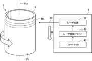
図4に示すように、本実施形態に係る露光装置2は、ロール原盤1の基材11の外周面に成膜されたレジスト層15を露光するための装置である。露光装置2は、レーザ光源21と、レーザ変調ドライバ30と、フォーマッタ40とを備える。
As shown in FIG. 4, the
レーザ光源21は、レーザ光20を発する光源であり、例えば、固体レーザまたは半導体レーザなどである。レーザ光20の波長は、特に限定されないが、例えば、400nm~500nmの青色光帯域の波長であってもよい。
The
フォーマッタ40は、上述した露光制御装置に相当する。フォーマッタ40は、オブジェクト130が描かれた入力画像110に基づいて、レジスト層15にレーザ光20を照射するための露光制御信号を生成する。例えば、フォーマッタ40は、基材11のレジスト層15の表面のうち、オブジェクト130に対応する位置に対してレーザ光20を照射するための露光制御信号を生成してもよい。これにより、基材11上のレジスト層15に、任意の形状のオブジェクト130に対応する潜像16が形成される。なお、フォーマッタ40は、レーザ光源21によるレーザ光20の発光を制御することで、基材11へのレーザ光20の照射を制御してもよく、レーザ光20が基材11に照射されないように照射位置を制御することで、基材11へのレーザ光20の照射を制御してもよい。
The
レーザ変調ドライバ30は、レーザ光源21によるレーザ光20の照射を制御するドライバである。レーザ変調ドライバ30は、レーザ光源21から照射されるレーザ光20の強度(パワー)を変調する機能を有する。レーザ変調ドライバ30には、上記フォーマッタ40により生成された露光制御信号が入力される。レーザ変調ドライバ30には、露光制御信号に基づいて、レーザ光源21から照射されるレーザ光20の強度を変調する。例えば図7に示したように、露光制御信号は、上記入力画像110の各小領域115に含まれるオブジェクト130の部分画像の濃淡(グレースケールの階調)に応じて、信号レベルが段階的に変化する階段状の波形を有する。このため、レーザ変調ドライバ30は、当該階段状の波形の露光制御信号の信号レベルに合わせて、レーザ光源21から照射されるレーザ光20の強度を変調する。この結果、レーザ光源21から基材11に対して、当該オブジェクト130の部分画像の濃淡に応じて強度が変調されたレーザ光20が照射され、レジスト層15が露光される。
The
以上のような構成の露光装置2は、基材11のレジスト層15に対してレーザ光20を照射することにより、レジスト層15の一部を変性させて、潜像16(図3B参照。)を形成する。かかる露光時に、露光装置2は、例えば、円筒形状の基材11の外周面に形成されたレジスト層15に対して、螺旋状の軌跡に沿ってレーザ光20を断続的に、または連続的に照射して、レジスト層15を螺旋状に露光してもよい。この場合、露光装置2は、円筒形状の基材11の中心軸11aを回転軸として基材11を一定速度で回転させながら、レーザ光20を基材11の中心軸11aに沿った一方向(R方向)に一定速度で走査するようにして、基材11にレーザ光20を照射してもよい。これにより、基材11の軸方向の一側から他側にかけて順次、レーザ光20が螺旋状の軌跡に沿ってレジスト層15の表面に断続的にまたは連続的に照射され、レジスト層15の表面のうち必要箇所に所望形状の潜像16が形成される。
The
本実施形態に係る露光装置2では、レーザ変調ドライバ30は、フォーマッタ40により生成された露光制御信号に基づいて、レーザ光20の強度を変調しながら、レーザ光20の照射を制御する。これにより、レーザ光20により露光されるレジスト層15の深さおよび形状を変化させて、オブジェクト130に対応する三次元形状を有する潜像16をレジスト層15に形成することができる。
In the
次に、図5を参照して、本実施形態に係るフォーマッタ40(露光制御装置)の機能構成について説明する。図5は、本実施形態に係るフォーマッタ40の構成を示すブロック図である。
Next, the functional configuration of the formatter 40 (exposure control device) according to this embodiment will be described with reference to FIG. 5. FIG. 5 is a block diagram showing the configuration of the
図5に示すように、本実施形態に係るフォーマッタ40は、レーザ光20の照射を制御するための露光制御信号とクロック信号を生成する。フォーマッタ40は、入力画像取得部401と、小領域分割部403と、信号生成部405と、クロック信号生成部407と、を備える。
As shown in FIG. 5, the
入力画像取得部401は、オブジェクト130が描かれた入力画像110(図6参照。)を取得する。入力画像110は、例えば、円筒形状の基材11の外周面を、当該基材11の軸方向に切り開いて、平面に展開した展開図に相当する画像である。また、入力画像110に描かれたオブジェクト130の平面形状は、例えば、円または楕円などの曲線を含む図形、三角形または四角形などの多角形、直線または曲線などの線状若しくは帯状、あるいは文字、記号を表す形状などであってもよい。
The input
小領域分割部403は、入力画像取得部401により取得された入力画像110を、所定の形状および大きさを有する複数の小領域115に分割する。具体的には、小領域分割部403は、入力画像110を所定の格子間隔で複数の小領域115に分割する。例えば、図6に示すように、小領域分割部403は、入力画像110を基材11の周方向に対応する方向(入力画像110のX方向)に所定の間隔Pxで分割するとともに、入力画像110を基材11の軸方向に対応する方向(入力画像110のY方向)に所定の間隔Pyで分割する。なお、間隔Pxと間隔Pyとは、同じであってもよく、異なっていてもよい。
The small
ここで、分割された小領域115の大きさ(例えば、上記間隔Px、Py)は、レーザ光20のスポットの大きさ(例えば、スポット径)よりも小さいことが好ましい。これにより、レーザ光20の照射により形成された潜像16を隣接した小領域115同士で隙間なく重ね合わせることができる。すなわち、露光装置2は、レーザ光20の複数のスポットを重ね合わせることで、オブジェクト130に対応する位置を塗りつぶすように露光することができる。例えば、レーザ光20のスポットの直径が、約200nmである場合、小領域115の間隔Px、Pyは、100nmであってもよく、小領域115は、100nm×100nmの正方形であってもよい。また、小領域115の形状は、正方形の例に限定されず、上述したように矩形状、三角形状、多角形状など、任意の形状であってもよい。
Here, it is preferable that the size of the divided small regions 115 (e.g., the intervals Px and Py) is smaller than the size of the spot of the laser light 20 (e.g., the spot diameter). This allows the
さらに、小領域分割部403は、小領域115の各々にオブジェクト130が含まれるか否かを判定する。また、小領域分割部403は、オブジェクト130が含まれる小領域115の各々内におけるオブジェクト130の部分画像の濃淡の度合い(グレースケールの階調)を判定する。
Furthermore, the small
ここで、図6を参照して、小領域分割部403の機能についてより詳細に説明する。図6は、複数の小領域115に分割された入力画像110を示す説明図である。なお、図6において、X方向は基材11の外周面の周方向に対応し、Y方向は基材11の軸方向に対応する。
The function of the small
図6に示すように、小領域分割部403は、オブジェクト130A、130B、130C、130Dを含む入力画像110をX方向に間隔Pxにて分割し、Y方向に間隔Pyにて分割している。これにより、入力画像110は、格子状の小領域115に分割される。また、小領域分割部403は、小領域115の各々にオブジェクト130が含まれるか否かを判定する。例えば、小領域分割部403は、小領域115Aをオブジェクト130が含まれない小領域であると判定し、小領域115Bおよび115Cをオブジェクト130が含まれる小領域であると判定する。なお、小領域分割部403は、各小領域115にわずかでもオブジェクト130が描かれている場合、該小領域115にオブジェクトが含まれると判定してもよい。あるいは、小領域分割部403は、各小領域115内の所定面積以上の領域にオブジェクト130が描かれている場合に、当該小領域115にオブジェクト130が含まれると判定してもよい。
6, the small
なお、入力画像110のうち一部領域のみを露光することを指示するために、入力画像110内に露光領域111が設定されていてもよい。この場合、小領域分割部403は、入力画像110のうち露光領域111内の小領域115に対してのみ、オブジェクト130が含まれるか否かを判定してもよい。
In addition, an
信号生成部405は、レーザ光20の照射を制御するための露光制御信号を生成する。具体的には、信号生成部405は、上記小領域分割部403の判定結果に基づいて、レジスト層15における各小領域115に対応する領域に、レーザ光20を照射するか否かを決定する。さらに、信号生成部405は、オブジェクト130が含まれる各小領域115内におけるオブジェクト130の部分画像の濃淡(例えば、グレースケールの階調)を段階的に判定する。そして、信号生成部405は、当該判定結果に基づいて、当該各小領域115に照射するレーザ光20の強度を段階的に決定する。さらに、信号生成部405は、当該決定結果(例えば、各小領域115に照射するレーザ光20の強度を表すデータ)に基づいて、各小領域115に照射するレーザ光20の強度とタイミングを示す露光制御信号を生成する。このとき、信号生成部405は、クロック信号生成部407が生成したクロック信号を用いて、上記決定したレーザ光20の強度を表すデータを、露光制御信号に変換する。このようにして信号生成部405により生成された露光制御信号は、レーザ光源21を制御するドライバ30に送信される。ドライバ30は、当該露光制御信号に基づいて、レーザ光源21によるレーザ光20の照射を制御する。
The
[2.4.入力画像と露光制御信号の具体例]
ここで、図6および図7を参照して、入力画像110に基づく露光制御信号の生成方法の具体例について、より詳細に説明する。なお、図7は、図6に示す入力画像110のうちオブジェクト130Aの周辺画像に対応する露光制御信号の具体例を示す説明図である。
[2.4. Specific examples of input image and exposure control signal]
6 and 7, a specific example of a method for generating an exposure control signal based on the
図6および図7に示すように、信号生成部405は、入力画像110のX方向の行ごとに、各小領域115内の部分画像の濃淡(例えばグレースケールの階調)を判定し、当該判定結果に基づいて、当該各小領域115に照射するレーザ光20の強度を決定する。
As shown in Figures 6 and 7, the
例えば、まず、信号生成部405は、入力画像110(または、露光領域111)の最も上の行を選択し、この行の左端の小領域115から順に右端の小領域115まで(即ち、X軸の正方向に向けて)、各小領域115内の部分画像の濃淡(例えば、グレースケールの階調)を判定する。
For example, first, the
このとき、信号生成部405は、オブジェクト130が含まれてない小領域115に対して、グレースケールの階調として「0」を割り当てる。一方、信号生成部405は、オブジェクト130が含まれる小領域115に対して、当該小領域115内のオブジェクト130の部分画像の濃淡に応じたグレースケールの階調の数値(例えば、図7の例では、「0~23」の24階調)を割り当てる。これにより、信号生成部405は、1つの行内の左端の小領域115から順に右端の小領域115まで、各小領域115のグレースケールの階調を判定する。
At this time, the
その後、信号生成部405は、一つ下の次の行を選択し、その行内で上記と同様な処理を行うことで、その行の各小領域115のグレースケールの階調を判定する。さらに、かかる判定処理を、上の行から順に下の行まで(Y方向の負方向に向けて)繰り返すことにより、入力画像110(または、露光領域111)全域内の複数の小領域115のグレースケールの階調を判定する。
Then, the
なお、信号生成部405が、入力画像110のX方向の各行においてグレースケールの階調を判定する順序は、基材11の回転方向に基づいて設定される。そのため、信号生成部405は、基材11の回転方向によっては、X方向の行ごとに右端の小領域115から順に左端の小領域115まで(X軸の負方向に向けて)、グレースケールの階調を判定してもよい。また、信号生成部405が、入力画像110のY方向に関し、グレースケールの階調を判定する順序は、基材11に対するレーザ光20の走査方向に基づいて設定される。そのため、信号生成部405は、基材11に対するレーザ光20の走査方向によっては、入力画像110の下の行から順に上の行まで(Y軸の正方向に向かって)、グレースケールの階調を判定してもよい。
The order in which the
また、図7に示すように、信号生成部405は、クロック信号生成部407から取得したクロック信号を用いて、上記各小領域115のグレースケールの階調の判定結果を表すデータ(各小領域115に照射するレーザ光20の強度を表すデータに相当する。)を、露光制御信号に変換する。例えば、クロック信号は所定の周波数を有する矩形波の信号である。また、当該グレースケールの階調の判定結果を表すデータは、例えば、入力画像110の各小領域115に割り当てられたグレースケールの階調を表す数値データである。
Also, as shown in FIG. 7, the
図7に示すように、露光制御信号は、階段状の波形を有する信号である、露光制御信号の信号レベルは、各小領域115の部分画像の濃淡を表すグレースケールの階調に応じて段階的に増減する。図7の例では、グレースケールの階調が「16」であると判定された小領域115に関し、露光制御信号の信号レベルが最も高くなっている。
As shown in FIG. 7, the exposure control signal is a signal having a stepped waveform, and the signal level of the exposure control signal increases and decreases in stages according to the grayscale gradation that represents the shade of the partial image of each
また、信号生成部405は、クロック信号に合わせて露光制御信号を生成する。例えば、露光制御信号の立ち上がりおよび立ち下りのタイミングが、クロック信号の立ち上がりまたは立ち下りのいずれかのタイミングと一致するように、露光制御信号が生成される。図7の例では、露光制御信号の立ち上がりおよび立ち下りがクロック信号の立ち上がりと一致するように、露光制御信号が生成されている。
The
クロック信号生成部407は、露光制御信号の基準となるクロック信号を生成する。具体的には、クロック信号生成部407は、基材11を回転させるスピンドルモータ35から、当該スピンドルモータ35の回転を制御するための回転制御信号を取得し、当該回転制御信号に基づいて、所定の周波数を有するクロック信号を生成する。
The clock
ここで、基材11を回転させるスピンドルモータ35の回転数は、一定の回転数を設定した場合であっても、常に一定ではなく、揺らいでいる。そのため、スピンドルモータ35の回転を制御する回転制御信号と、レーザ光20の照射を制御する露光制御信号とが同期していない場合、スピンドルモータ35の1回転と、露光制御信号の1周分とが一致しない可能性がある。このような場合、レーザ光20が照射される基材11の外周面の位置が、基材11の1回転ごとにずれるため、オブジェクト130に対応する凹凸パターンを基材11の外周面の正確な位置に形成できない恐れがある。
Here, the rotation speed of the
そこで、本実施形態に係る露光装置2では、上述したように、スピンドルモータ35の回転を制御するための回転制御信号からクロック信号を生成し、該クロック信号に基づいて、レーザ光20の照射を制御するための露光制御信号を生成する。これにより、回転制御信号と露光制御信号を同期させている。したがって、レーザ光20が照射される基材11の外周面の位置が、基材11の1回転ごとにずれないので、オブジェクト130に対応する凹凸パターンを基材11の外周面の正確な位置に形成することができる。
As described above, in the
なお、回転制御信号と露光制御信号とを同期させる方法は、上記の例に限定されない。例えば、クロック信号生成部407は、基準となるクロック信号をそれぞれスピンドルモータ35および信号生成部405に送信してもよい。このような場合、スピンドルモータ35は、該クロック信号を基にスピンドルモータ35の回転を制御する回転制御信号を生成し、信号生成部405は、該クロック信号を基に露光制御信号を生成する。この方法によっても、スピンドルモータ35の回転を制御する回転制御信号と、レーザ光20の照射を制御する露光制御信号とを同期させることができる。
The method of synchronizing the rotation control signal and the exposure control signal is not limited to the above example. For example, the clock
以上にて、レーザ光20の照射を制御する露光制御信号を生成するフォーマッタ40の機能構成について説明した。このようなフォーマッタ40によれば、任意のオブジェクト130の三次元形状に対応する露光制御信号を好適に生成することができる。
The above describes the functional configuration of the
なお、このようなフォーマッタ40の機能は、ソフトウェアとハードウェアとの協働によって実現される。例えば、フォーマッタ40は、ブリッジにて相互に接続されたCPU(Central Processing Unit)、ROM(Read Only Memory)、RAM(Random Access Memory)等を備え、これらのハードウェアによって上記の機能を実現してもよい。
The functions of the
例えば、CPUは、演算処理装置および制御装置として機能し、各種プログラムに従って、フォーマッタ40内の動作全般を制御する。ROMは、CPUが使用するプログラム、演算パラメータを記憶し、RAMは、CPUの実行において使用するプログラムや、その実行において適宜変化するパラメータ等を一時記憶する。これにより、CPUは、例えば、入力画像取得部401、小領域分割部403、信号生成部405、クロック信号生成部407の機能を実行することができる。
For example, the CPU functions as an arithmetic processing unit and control unit, and controls the overall operation within the
[2.5.入力画像と露光制御信号の別の具体例]
次に、図8~図10を参照して、入力画像110に基づく露光制御信号の生成方法の別の具体例について、より詳細に説明する。なお、図8は、本実施形態に係る入力画像110の具体例を示す説明図である。図9は、複数の小領域115に分割された入力画像110と、オブジェクト130の部分画像の濃淡(グレースケールの階調)の具体例を示す説明図である。図10は、図9に示す入力画像110のうち1つのオブジェクト130(マイクロレンズ)の部分画像に対応する露光制御信号の具体例を示す説明図である。
[2.5. Another specific example of input image and exposure control signal]
Next, another specific example of a method for generating an exposure control signal based on an
なお、図8~図10の具体例でも、上述した図6および図7の具体例と同様に、入力画像110が複数の小領域115に分割され、各小領域115の部分画像の濃淡(グレースケールの階調)に基づいて、露光制御信号が生成される。よって、これらの分割処理および生成処理の詳細説明は省略する。
In the specific examples of Figures 8 to 10, as in the specific examples of Figures 6 and 7 described above, the
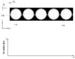
図8および図9に示すように、入力画像110は、同一の形状を有する複数のオブジェクト130が描かれたグレースケール画像であってもよい。図8の例の入力画像110は、マイクロレンズアレイを表しており、個々のマイクロレンズはオブジェクト130に相当する。図8に示すように、オブジェクト130として複数のマイクロレンズが縦横(XおよびY方向)に正方格子状に規則的に配列されている。複数のマイクロレンズは、相互に間隔を空けて配置されている。図8の例のマイクロレンズ(オブジェクト130)は、球面または非球面形状を有する凸レンズであり、当該マイクロレンズの表面形状は、レンズ頂点に近いほど高くなる三次元形状を有する。このため、図9に示すように、入力画像110のうちマイクロレンズが存在する領域では、レンズ頂点に近いほど、マイクロレンズの画像の濃淡は白色に近くなり、グレースケールの階調が大きくなっている(例えば、階調=「1」~「16」)。一方、相隣接する複数のマイクロレンズの間の非レンズ領域は、高さが低い平坦面となっており、当該非レンズ領域の画像の濃淡は黒色に近くなり、グレースケールの階調が最も小さくなっている(例えば、階調=「0」)。
8 and 9, the
図9の上側に示す入力画像110は、図8の入力画像110から、Y方向の中央の1行に配列された5個のマイクロレンズ(オブジェクト130)の部分画像を切り出したものである。図9に示すように、入力画像110が、正方格子状のグリッド線により、複数の小領域115に分割されている。図9の例では、X方向のグリッド線の間隔Pxと、Y方向のグリッド線の間隔Pyとは等しく、小領域115は正方形のグリッドとなっている。しかし、かかる例に限定されず、例えば、間隔Pxと間隔Pyは互いに異なってもよく、小領域115は、矩形状または他の形状を有するグリッドであってもよい。
The
図9に示すように、入力画像110中で1つのマイクロレンズ(オブジェクト130)が存在する領域を、マイクロレンズの三次元形状の高低差に応じて、例えば100個以上の多数の小領域115に分割することが好ましい(例えば、X方向に10分割以上、Y方向に10分割以上)。これにより、当該多数の小領域115の部分画像を用いて、個々のマイクロレンズの三次元的な球面または非球面形状を、原盤1の基材11の外周面に緻密かつ滑らかに再現することが可能になる。
As shown in FIG. 9, it is preferable to divide the area in the
また、図9の下側に示す棒グラフは、図9の上側の入力画像110のうち、Y方向のほぼ中央において5個のマイクロレンズをX方向に横断する1行の部分画像の濃淡(例えば、グレースケールの階調)の変化を示している。このように、入力画像110を小領域115に分割した上で、各小領域115の部分画像を解析することにより、各小領域115の部分画像の濃淡を求める。これにより、入力画像110で二次元的に描かれているマイクロレンズの三次元形状の高さの変化を的確に把握して、露光制御信号に反映させることが可能になる。したがって、図10に示すように、各小領域115の部分画像の濃淡(グレースケールの階調)から、マイクロレンズの三次元形状に対応した露光制御信号を生成することができる。
The bar graph shown at the bottom of FIG. 9 shows the change in the shading (e.g., grayscale gradation) of one row of partial images that cross five microlenses in the X direction at approximately the center in the Y direction of the
図10に示す露光制御信号は、上述した図7の例の露光制御信号と同様に、マイクロレンズ(オブジェクト130)の部分画像の濃淡を表すグレースケールの階調に応じた階段状の波形を有する。グレースケールの階調が大きいほど、露光制御信号の信号レベルが高い値に設定されている。この露光制御信号の信号レベルの変化は、1つのマイクロレンズの三次元形状の高さの変化に対応している。当該露光制御信号を用いてレーザ光20の強度を変調しながらレジスト層15を露光することで、マイクロレンズアレイの三次元形状に対応するレジストパターン17を、レジスト層15に的確に再現することができる。
The exposure control signal shown in FIG. 10 has a stepped waveform corresponding to the grayscale gradation representing the shade of the partial image of the microlens (object 130), similar to the exposure control signal in the example of FIG. 7 described above. The higher the grayscale gradation, the higher the signal level of the exposure control signal is set to. The change in the signal level of this exposure control signal corresponds to the change in the height of the three-dimensional shape of one microlens. By exposing the resist
以上、図8~図10を参照して、オブジェクト130として複数のマイクロレンズが規則的に配列されたマイクロレンズアレイを表す入力画像110と、当該入力画像110に基づいて生成された露光制御信号の具体例について説明した。かかる具体例によれば、当該入力画像110に描かれたマイクロレンズアレイを製造するための原盤1を製造することができる。当該製造方法によれば、例えば図8に示した入力画像110に二次元的に描かれたマイクロレンズアレイの三次元形状に対応する凹凸構造13を、原盤1の外周面に高精度で再現することができる。
Above, with reference to Figs. 8 to 10, an
なお、原盤1による製造対象の製品は、上記図8等に示したマイクロレンズアレイの例に限定されず、多様な製品に適用可能である。例えば、原盤1による製造対象の製品は、複数のマイクロレンズが不規則に配置されたマイクロレンズアレイであってもよいし、あるいは、可視光帯域に属する波長以下の凹凸周期を有するモスアイ構造が形成された反射防止フィルム、拡散板、偏光板、回折格子、その他各種の光学部材などであってもよい。これら各種の光学部材に形成される所望の凹凸構造を、オブジェクト130としてグレースケールで描画した入力画像110を生成し、本実施形態に係る原盤1の製造方法に当該入力画像110を適用すればよい。これにより、当該所望の凹凸構造を有する光学部材の製品を製造するために用いる原盤1を、容易かつ高精度で製造可能である。
The product to be manufactured using the
[2.6.露光装置の構成例]
次に、図11および図12を参照して、本実施形態に係る原盤1の製造方法に使用される露光装置2の構成例について説明する。図11は、本実施形態に係る露光装置2Aの構成例を示す説明図である。図12は、本実施形態に係る露光装置2Bの他の構成例を示す説明図である。
[2.6. Configuration example of exposure apparatus]
Next, a configuration example of an
まず、図11を参照して、本実施形態に係る露光装置2Aについて説明する。露光装置2Aは、レーザ光源21Aとして、固体レーザを用いる露光装置である。
First, the
図11に示すように、露光装置2Aは、レーザ光源21Aと、電気光学素子(Electro Optical Modulator:EOM)22と、第1ミラー23と、フォトダイオード(Photodiode:PD)24と、変調光学系25と、制御機構37と、第2ミラー31と、移動光学テーブル32と、スピンドルモータ35と、ターンテーブル36とを備える。また、基材11は、ターンテーブル36上に載置され、回転することができるようになっている。
As shown in FIG. 11, the
レーザ光源21Aは、具体的には、固体レーザである。例えば、レーザ光源21Aとして、266nmの波長を有する固体レーザなどを用いることができる。
The
レーザ光源21Aから出射されたレーザ光20は、平行ビームのまま直進し、電気光学素子22に入射する。電気光学素子22を透過したレーザ光20は、第1ミラー23で反射され、変調光学系25に導かれる。
The
第1ミラー23は、偏光ビームスプリッタで構成されており、偏光成分の一方を反射させ、偏光成分の他方を透過させる機能を有する。第1ミラー23を透過した偏光成分は、フォトダイオード24によって受光され、光電変換される。また、フォトダイオード24によって光電変換された受光信号は、電気光学素子22に入力される。電気光学素子22は、入力された受光信号に基づいてレーザ光20の位相変調を行う。
The
また、変調光学系25は、集光レンズ26と、音響光学素子(Acousto-Optic Modulator:AOM)27と、コリメータレンズ28とを備える。
The modulation
変調光学系25において、レーザ光20は、集光レンズ26によって、ガラス(SiO2)などからなる音響光学素子27に集光される。レーザ光20は、音響光学素子27によって強度変調され発散した後、コリメータレンズ28によって、再度、平行ビーム化される。変調光学系25から出射されたレーザ光20は、第2ミラー31によって反射され、移動光学テーブル32上に水平かつ平行に導かれる。
In the modulation
また、制御機構37は、フォーマッタ40と、ドライバ30とを備え、レーザ光20の照射を制御する。フォーマッタ40は、上述したようにレーザ光20の照射を制御するための露光制御信号を生成し、ドライバ30は、フォーマッタ40が生成した露光制御信号に基づいて、音響光学素子27を制御する。これにより、レジスト層15へのレーザ光20の照射が制御される。
The
移動光学テーブル32は、ビームエキスパンダ(Beam expader:BEX)33と、対物レンズ34とを備える。移動光学テーブル32に導かれたレーザ光20は、ビームエキスパンダ33により所望のビーム形状に整形された後、対物レンズ34を介して、基材11の外周面のレジスト層15に照射される。
The moving optical table 32 includes a beam expander (BEX) 33 and an
なお、図示していないが、露光装置2Aは、レーザ光20が常に基材11上のレジスト層15にて焦点を結ぶように動的にフォーカス制御されることが好ましい。具体的には、基材11は、回転の際に、回転軸の軸ぶれ、および基材11の表面の加工精度等によって対物レンズ34から基材11までの距離が変動している。そのため、レーザ光20が常に基材11のレジスト層15にて焦点を結ぶようにするために、露光装置2Aは、レーザ光20のフォーカスずれを検出し、動的にレーザ光20のフォーカスを制御することが好ましい。なお、基材11上のレジスト層15に対するレーザ光20のフォーカスずれを検出する方法は、例えば、レジスト層15に照射したレーザ光20の反射光の非点収差を検出する方法などを用いることができる。
Although not shown, it is preferable that the
これらの構成により、ターンテーブル36により基材11を一定速度で回転させ、レーザ光20を基材11の軸方向に一定速度で走査しながら照射することにより、レジスト層15が露光される。なお、レーザ光20の走査は、移動光学テーブル32により、レーザ光20を矢印R方向へ一定速度で移動させることによって行われる。
With this configuration, the
なお、上記で説明したように、露光装置2Aでは、レーザ光20の実際の照射位置と、露光制御信号が示す照射位置とが一致する(同期する)ように、スピンドルモータ35の回転を制御するための回転制御信号と、レーザ光20の照射を制御するための露光制御信号とが同期されている。これにより、露光装置2Aは、基材11の1周ごとにレーザ光20の照射位置がずれることなくレジスト層15を露光することができる。
As described above, in the
また、露光装置2Aのターンテーブル36の回転数、フォーマッタ40が生成する露光制御信号の周波数は、基材11の円筒形状の外周長さ、および入力画像110の周方向(X方向)の分割間隔Pxにより決定される。さらに、露光装置2Aの移動光学テーブル32の送りピッチは、入力画像110の軸方向(Y方向)の分割間隔Pyにより決定される。すなわち、これらの露光パラメータは、レーザ光20の照射位置が入力画像110の分割された小領域と一致するように決定される。
The rotation speed of the
次に、図12を参照して、本実施形態の別の構成例に係る露光装置2Bについて説明する。露光装置2Bは、レーザ光源21Bとして、半導体レーザを用いる露光装置である。
Next, with reference to FIG. 12, an
図12に示すように、露光装置2Bは、レーザ光源21Bと、第1ミラー23と、フォトダイオード(PD)24と、集光レンズ26と、電気光学偏向素子(Electro Optic Deflector:EOD)29と、コリメータレンズ28と、制御機構37と、第2ミラー31と、移動光学テーブル32と、スピンドルモータ35と、ターンテーブル36とを備える。また、基材11は、ターンテーブル36上に載置され、回転することができるようになっている。
As shown in FIG. 12, the
ここで、移動光学テーブル32、スピンドルモータ35、およびターンテーブル36については、図11を参照して説明した露光装置2Aと同様であるので、ここでの説明は省略する。
The movable optical table 32,
レーザ光源21Bは、具体的には、半導体レーザである。例えば、レーザ光源21Bとして、400nm~500nmの青色光帯域の波長のレーザ光を発する青色半導体レーザを用いることができる。本実施形態に係る製造方法にて使用される露光装置では、レーザ光源21Bとして、半導体レーザを用いることが好ましい。
The
レーザ光源21Bから出射されたレーザ光20は、平行ビームのまま直進し、第1ミラー23で反射される。また、第1ミラー23にて反射されたレーザ光20は、集光レンズ26によって電気光学偏向素子29に集光された後、コリメータレンズ28によって、再度、平行ビーム化される。平行ビーム化されたレーザ光20は、第2ミラー31によって反射され、移動光学テーブル32上に水平かつ平行に導かれる。
The
第1ミラー23は、偏光ビームスプリッタで構成されており、偏光成分の一方を反射させ、偏光成分の他方を透過させる機能を有する。第1ミラー23を透過した偏光成分は、フォトダイオード24によって受光され、光電変換される。また、フォトダイオード24によって光電変換された受光信号は、レーザ光源21Bに入力される。レーザ光源21Bは、入力された受光信号に基づいてレーザ光20の変調を行う。
The
電気光学偏向素子29は、レーザ光20の照射位置を制御することが可能な素子である。露光装置2Bは、電気光学偏向素子29により、移動光学テーブル32上に導かれるレーザ光20の照射位置を変化させることも可能である。
The electro-
また、制御機構37は、フォーマッタ40と、ドライバ30とを備え、レーザ光20の照射を制御する。ドライバ30は、フォーマッタ40が生成した露光制御信号に基づいてレーザ光源21Bの出力を制御する。これにより、レジスト層15へのレーザ光20の照射が制御される。
The
なお、図12で示した露光装置2Bは、図11で示した露光装置2Aと同様に、レーザ光20のフォーカスを動的に制御しており、スピンドルモータ35の回転制御信号と、レーザ光20の露光制御信号とを同期させている。
Note that the
[3.まとめ]
以上、本実施形態に係る原盤1の製造方法、当該製造方法に用いられる原盤1の製造装置、並びに、転写物およびレプリカ原盤の製造方法などについて詳細に説明した。本実施形態によれば、任意の入力画像110に描かれたオブジェクト130の画像の濃淡(例えばグレースケールの階調)に応じて、レーザ光20の強度を変調し、当該強度が変調されたレーザ光20を用いて、基材11の外周面のレジスト層15を露光する。かかる露光方法により、オブジェクト130の任意の三次元形状に対応するレジストパターン17を、レジスト層15に形成できる。したがって、当該レジストパターン17を用いて基材11の外周面をエッチング等することにより、当該三次元形状に対応する凹凸構造13を基材11の外周面に形成することができる。よって、本実施形態によれば、従来技術と比べて、原盤1の基材11の外周面に、任意の三次元形状を有するオブジェクト130に対応する凹凸構造13のパターンを高精度に形成することができる。
3. Summary
The above has described in detail the manufacturing method of the
より詳細には、上記特許文献1に開示された技術では、区画された露光対象領域毎に露光を行っており、当該露光対象領域は、露光光の強度が小さく、露光深さの浅い凹部同士の境界部分で区画されていた。このため、隣り合う区画の凹凸構造同士が連続的にシームレスに連結されるような任意の三次元形状を有する凹凸構造を自由に形成することができないという問題があった。
More specifically, in the technology disclosed in
これに対し、本実施形態によれば、入力画像110におけるオブジェクト130の配置や凹凸形状とは無関係に、入力画像110を複数の小領域115に分割するためのグリッド線を自由に設定することができる。このように小領域115の分割方法の自由度が高いため、オブジェクト130の配置や凹凸形状に柔軟に対応した露光制御信号を生成して、レジスト層15の露光に利用できる。よって、任意の三次元形状を有するオブジェクト130に対応する凹凸構造13を、原盤1の外周面に自由に形成することが可能である。
In contrast, according to this embodiment, grid lines for dividing the
また、上記特許文献1に記載の技術では、露光光として、入力画像110に応じて強度が変調されたレーザ光のスポットを断続的に照射するのではなく、露光光をレジスト膜の面方向に相対移動させて連続的に照射する走査露光を行っていた。このため、かかる連続的な走査露光では、所望の三次元形状の凹凸構造のパターンを高精度で形成することが困難であるという問題があった。
In addition, in the technology described in
これに対し、本実施形態によれば、露光光として、入力画像110の濃淡に応じて強度が変調されたレーザ光20のスポットを使用し、入力画像110の小領域115に対応するレジスト層15の各領域に対して、レーザ光20のスポットを断続的または連続的に照射する。この際、入力画像110の小領域115ごとにレーザ光20の強度を変調しつつ、当該小領域115に対応するレジスト層15の各領域に対して、強度が変調されたレーザ光20のスポットを照射する。ここで、小領域115の大きさ(例えば、面積または間隔Px、Pcなど)は、レジスト層15に照射されるレーザ光20のスポットの大きさ(例えば、照射面積またはスポット径など)よりも小さいことが好ましい。かかる階調露光方法により、入力画像110に描かれたオブジェクト130の高さ、三次元形状および配置に合わせて、レジスト層15を所望の深さ、三次元形状および配置で好適に露光できる。したがって、オブジェクト130に対応する複数の潜像16からなるレジストパターン17を高精度かつ自由に形成することができる。よって、当該レジストパターン17を用いて、原盤1の基材11の外周面に、所望の三次元形状を有する凹凸構造13のパターンを高精度かつ自由に形成することができる。
In contrast, according to the present embodiment, a spot of
また、上記特許文献2に記載された技術では、ロール原盤の外周面のレジスト層を露光するとき、レーザ光の強度を変調しておらず、一定の強度のレーザ光をオン/オフすることで、凹凸パターンを露光していた。したがって、凹凸構造のパターンの深さを任意に変化させることができないため、任意の三次元形状を有する凹凸構造を自由に形成することが困難であるという問題があった。
In addition, in the technology described in
これに対し、本実施形態によれば、入力画像110中のオブジェクト130の部分画像の濃淡(例えば、グレースケールの階調)に合わせて、レジスト層15に照射するレーザ光20の強度を自由に変調可能である。したがって、レジスト層15の露光時に、所望の三次元形状を有するレジストパターン17を適切に形成できる。よって、当該レジストパターン17を用いて原盤1の外周面に形成される微細な凹凸構造13の深さや三次元形状、配置を、所望のオブジェクト130の三次元形状のパターンに合わせて自由に変化させることができる。
In contrast, according to this embodiment, the intensity of the
さらに、本実施形態に係る製造方法により製造される原盤1は、円筒形状または円柱形状を有するロール原盤であって、その外周面に、任意の三次元形状を有する凹凸構造13が形成されている。ここで、凹凸構造13の三次元形状は、例えば、図1および図6に示すように任意のオブジェクト130に対応する多様な形状であってもよいし、図8および図9に示すように、複数のマイクロレンズ(個々のマイクロレンズは、オブジェクト130の一例である。)が規則的または不規則に配列されたマイクロレンズアレイなどの光学部材の凹凸形状であってもよい。
Furthermore, the
かかるロール原盤1を用いて転写物を製造することにより、上記のような任意の三次元形状を有する凹凸構造13が表面に転写された転写物(例えば、マイクロレンズアレイが形成された光学シート)の生産性と品質を向上することができる。さらに、本実施形態では、ロール原盤1を備えた製造装置を用いて、ロールツーロール方式で転写物を製造する。これにより、平板形原盤を備えた従来の製造装置と比べて、マイクロレンズアレイ等の微細凹凸構造を備えた製品を、安価かつ高い生産性で製造することが可能となる。
By manufacturing a transfer product using such a
以下に、上述した本実施形態に係る原盤の製造方法の実施例について、具体的に説明する。なお、以下に示す実施例は、上記実施形態に係る原盤の製造方法の実施可能性および効果を示すための一例であり、本発明に係る原盤の製造方法が以下の実施例に限定されるものではない。 Below, we will specifically explain examples of the method for manufacturing a master disk according to the present embodiment described above. Note that the examples shown below are examples intended to demonstrate the feasibility and effects of the method for manufacturing a master disk according to the above embodiment, and the method for manufacturing a master disk according to the present invention is not limited to the following examples.
以下の製造方法により、本発明の実施例1~4に係る原盤1と転写物を製造した。
The
(実施例1:図13)
まず、実施例1に係る原盤1と転写物の製造方法について説明する。
(Example 1: FIG. 13)
First, a method for manufacturing the
レジスト成膜工程(S10)にて、円筒形状の基材11の外周面に、ディップコート法により厚み10μmのレジスト層15を形成した。基材11としては4.5mm厚の円筒形状の石英ガラスからなる基材を用いた。レジスト材料としては、有機系レジストであるポジ型フォトレジスト(例えば、製品名:「AZ-P4210」、Merc社製)を用いた。
In the resist film formation step (S10), a resist
次いで、露光制御信号生成工程(S20)にて、入力画像110を用いて露光制御信号を生成した。入力画像110(露光パターン)としては、図13に示すように、同一形状を有する複数のマイクロレンズ(オブジェクト130に相当する。)が正方格子状に規則的に配列されたマイクロレンズアレイのグレースケール画像を使用した。このマイクロレンズアレイでは、直径20μm、高さ4μmのマイクロレンズが、20μmピッチで、相互の間にほぼ隙間なく整列されている。入力画像110を複数の小領域115に分割する間隔Px、Py(図9参照。)は、200nmとした。マイクロレンズの部分画像の濃淡を示すグレースケールの階調は、256階調とした。
Next, in the exposure control signal generating step (S20), an exposure control signal was generated using the
その後、露光工程(S30)にて、露光制御信号に基づいてレーザ光20の強度を変調しながら、基材11の外周面に成膜されたレジスト層15を露光した。具体的には、図12に示す露光装置2Bを用いて、レーザ光20による光リソグラフィにより、基材11のレジスト層15に潜像16を形成した。露光装置2Bのレーザ光源21Bには、波長405nmのレーザ光20を発する青色半導体レーザを用いた。また、露光時には、中心軸11aを中心に基材11を900rpmで回転させながら、レーザ光20を基材11の軸方向に1.5μm/秒にて走査した。
After that, in the exposure step (S30), the resist
次いで、現像工程(S40)にて、上記露光後の基材11を現像した。この現像工程では、TMAHの2.38質量%水溶液を用いて、27℃にて1800秒間現像し、露光した部分のレジストを溶解させ、レジストパターン17を形成した。
Next, in the development step (S40), the exposed
その後、エッチング工程(S50)にて、上記現像後のレジストパターン17をマスクとして用いて、基材11をドライエッチングした。このエッチング工程では、エッチングガスとしてCHF3ガス(流量30sccm)を用い、チャンバーのガス圧0.5Pa、印加RF電力150Wにて、エッチング時間300分間で、反応性イオンエッチングを行った。かかるエッチング工程により、基材11の外周面に凹凸構造13を形成した。
Thereafter, in an etching step (S50), the
以上の工程により、実施例1に係る原盤1を製造した。さらに、製造した原盤1を用いて、実施例1に係る転写物を製造した。具体的には、図2で示したような転写装置6を用いて、転写物のシート状基材(被転写物61)の表面に、紫外線硬化樹脂からなる樹脂層62を積層し、原盤1の外周面に形成された凹凸構造13を未硬化の樹脂層62に転写した。なお、転写物のシート状基材には、ポリエチレンテレフタレート(PolyEthylene Terephthalate:PET)フィルムを用いた。その後、メタルハライドランプにより、1000mJ/cm2の紫外線を1分間照射することで、紫外線硬化樹脂からなる樹脂層62を硬化させた。このようにして、原盤1の凹凸構造13が樹脂層62に転写された転写物(マイクロレンズアレイの製品)を製造した。
The
上記のように製造された実施例1に係る転写物である整列マイクロレンズアレイのSEM画像を、図13の下部側に示す。図13に示すように、実施例1に係る整列マイクロレンズアレイでは、入力画像110に描かれた複数のマイクロレンズ(オブジェクト130)からなるマイクロレンズアレイの三次元形状が、転写物の表面に高精度で再現されていることが分かる。
The lower part of Figure 13 shows an SEM image of the aligned microlens array, which is the transfer product of Example 1 manufactured as described above. As shown in Figure 13, in the aligned microlens array of Example 1, it can be seen that the three-dimensional shape of the microlens array consisting of multiple microlenses (object 130) depicted in the
(実施例2:図14)
次に、実施例2に係る原盤1と転写物の製造方法について説明する。実施例2では、露光制御信号生成工程(S20)で用いる入力画像110以外は、実施例1と同様な製造方法で、原盤1と転写物を製造した。
(Example 2: FIG. 14)
Next, a description will be given of a manufacturing method of the
実施例2(図14)では、実施例1(図13)と比べて大きい配列ピッチでマイクロレンズが配列された整列マイクロレンズアレイを製造するための入力画像110を用いた。実施例2に係る入力画像110としては、図14に示すように、同一形状を有する複数のマイクロレンズ(オブジェクト130に相当する。)が正方格子状に規則的に配列されたマイクロレンズアレイのグレースケール画像を使用した。このマイクロレンズアレイでは、直径25μm、高さ3μmのマイクロレンズが、25μmピッチで、相互に間隔を空けて整列されている。入力画像110を複数の小領域115に分割する間隔Px、Py(図9参照。)は、200nmとした。マイクロレンズの部分画像の濃淡を示すグレースケールの階調は、256階調とした。
In Example 2 (FIG. 14), an
実施例2に係る転写物である整列マイクロレンズアレイのSEM画像を、図14の下部側に示す。図14に示すように、実施例2に係る整列マイクロレンズアレイでも、入力画像110に描かれた複数のマイクロレンズ(オブジェクト130)からなるマイクロレンズアレイの三次元形状が、転写物の表面に高精度で再現されていることが分かる。
An SEM image of the aligned microlens array, which is a transfer product according to Example 2, is shown in the lower part of Fig. 14. As shown in Fig. 14, it can be seen that the three-dimensional shape of the microlens array consisting of a plurality of microlenses (object 130) depicted in the
(実施例3:図15)
次に、実施例3に係る原盤1と転写物の製造方法について説明する。実施例3では、露光制御信号生成工程(S20)で用いる入力画像110以外は、実施例1と同様な製造方法で、原盤1と転写物を製造した。
(Example 3: FIG. 15)
Next, a description will be given of a manufacturing method of the
実施例3(図15)では、複数のマイクロレンズが不規則に配置されたランダムマイクロレンズアレイを製造するための入力画像110を用いた。実施例3に係る入力画像110としては、図15に示すように、ほぼ同一形状を有する複数のマイクロレンズ(オブジェクト130に相当する。)が、ランダムに配置されたマイクロレンズアレイのグレースケール画像を使用した。このマイクロレンズアレイでは、概ね直径10μm、高さ3μmのマイクロレンズが、ある程度分散してランダムに配置されている。入力画像110を複数の小領域115に分割する間隔Px、Py(図9参照。)は、200nmとした。マイクロレンズの部分画像の濃淡を示すグレースケールの階調は、256階調とした。
In Example 3 (FIG. 15), an
実施例3に係る転写物であるランダムマイクロレンズアレイのSEM画像を、図15の下部側に示す。図15に示すように、実施例3に係るに係るランダムマイクロレンズアレイでは、入力画像110に描かれた複数のマイクロレンズ(オブジェクト130)からなるマイクロレンズアレイの三次元形状が、転写物の表面に高精度で再現されていることが分かる。
The SEM image of the random microlens array, which is the transfer product of Example 3, is shown in the lower part of Figure 15. As shown in Figure 15, in the random microlens array of Example 3, it can be seen that the three-dimensional shape of the microlens array consisting of multiple microlenses (object 130) depicted in the
(実施例4:図16)
次に、実施例4に係る原盤1と転写物の製造方法について説明する。実施例4では、露光制御信号生成工程(S20)で用いる入力画像110以外は、実施例1と同様な製造方法で、原盤1と転写物を製造した。
(Example 4: FIG. 16)
Next, a description will be given of a manufacturing method of the
実施例4(図16)では、実施例3(図15)と比べて多数のマイクロレンズが密集して不規則に配置されたランダムマイクロレンズアレイを製造するための入力画像110を用いた。実施例4に係る入力画像110としては、図16に示すように、相異なる形状を有する複数のマイクロレンズ(オブジェクト130に相当する。)が、ランダムに配置されたマイクロレンズアレイのグレースケール画像を使用した。このマイクロレンズアレイでは、概ね直径10μm、高さ2μmのマイクロレンズが、相互に隙間なく密集しつつ、ランダムに配置されている。入力画像110を複数の小領域115に分割する間隔Px、Py(図9参照。)は、200nmとした。マイクロレンズの部分画像の濃淡を示すグレースケール画像の階調は、256階調とした。
In Example 4 (FIG. 16), an
実施例4に係る転写物であるランダムマイクロレンズアレイのSEM画像を、図16の下部側に示す。図16に示すように、実施例4に係るランダムマイクロレンズアレイでも、入力画像110に描かれた複数のマイクロレンズ(オブジェクト130)からなるマイクロレンズアレイの三次元形状が、転写物の表面に高精度で再現されていることが分かる。
The SEM image of the random microlens array, which is the transfer product of Example 4, is shown in the lower part of Figure 16. As shown in Figure 16, it can be seen that the three-dimensional shape of the microlens array consisting of multiple microlenses (object 130) depicted in the
以上の実施例1~4の結果によれば、本実施形態に係る原盤の製造方法によって、原盤1の外周面に、任意の三次元形状を有するマイクロレンズアレイの微細な凹凸構造13のパターンを高精度で形成できることが確認された。さらに、当該原盤1を用いた転写物の製造方法によって、原盤1の凹凸構造13を転写物に高精度で転写して、各種のマイクロレンズアレイの製品を安価かつ効率的に量産できることが確認された。
The results of Examples 1 to 4 above confirmed that the method for manufacturing a master according to this embodiment makes it possible to form a pattern of the fine
以上、添付図面を参照しながら本発明の好適な実施形態について詳細に説明したが、本発明はかかる例に限定されない。本発明の属する技術の分野における通常の知識を有する者であれば、特許請求の範囲に記載された技術的思想の範疇内において、各種の変更例または修正例に想到し得ることは明らかであり、これらについても、当然に本発明の技術的範囲に属するものと了解される。 The above describes in detail preferred embodiments of the present invention with reference to the attached drawings, but the present invention is not limited to such examples. It is clear that a person with ordinary knowledge in the technical field to which the present invention pertains can conceive of various modified or revised examples within the scope of the technical ideas described in the claims, and it is understood that these also naturally fall within the technical scope of the present invention.
なお、本実施形態に係る製造方法により製造された原盤1とその転写物は、任意の三次元形状の凹凸構造を好適に実現できるため、様々な用途に適用することができる。
The
例えば、転写物は、転写された凹凸構造に回路を形成することで、プリンテッド・エレクトロニクスに適用することができる。他の例としては、転写物は、転写された凹凸構造に血液等の生体試料の流路を形成することにより、バイオセンサまたは診断デバイスに適用することができる。また、転写物は、転写された凹凸構造により光学的特性を制御することにより、光学素子に適用することができる。さらに、転写物は、転写された凹凸構造を用いることにより、粒子配列シートに適用することができる。 For example, the transfer material can be applied to printed electronics by forming a circuit in the transferred concave-convex structure. As another example, the transfer material can be applied to biosensors or diagnostic devices by forming a flow path for biological samples such as blood in the transferred concave-convex structure. The transfer material can also be applied to optical elements by controlling the optical properties with the transferred concave-convex structure. Furthermore, the transfer material can be applied to particle array sheets by using the transferred concave-convex structure.
1 原盤
2、2A、2B 露光装置
6 転写装置
11 基材
12、12A、12B、12C 凹部
13 凹凸構造
15 レジスト層
16 潜像
17 レジストパターン
18 凹部
20 レーザ光
21 レーザ光源
30 ドライバ(レーザ変調ドライバ)
40 フォーマッタ(露光制御装置)
110 入力画像
115 小領域
401 入力画像取得部
403 小領域分割部
405 信号生成部
407 クロック信号生成部
REFERENCE SIGNS
40 Formatter (exposure control device)
110
Claims (11)
三次元形状を有する少なくとも1つのオブジェクトが二次元的に描かれた入力画像を複数の小領域に分割する工程と、
前記小領域の各々に前記オブジェクトが含まれるか否かに基づいて、前記小領域の各々にレーザ光を照射するか否かを決定するとともに、前記オブジェクトが含まれる前記小領域の各々内における前記オブジェクトの部分画像の濃淡に基づいて、当該小領域の各々に照射するレーザ光の強度を段階的に決定し、当該決定結果に基づいて、前記オブジェクトに対応する露光制御信号を生成する工程と、
前記露光制御信号に基づいて、前記小領域ごとに前記オブジェクトの前記部分画像の濃淡に応じて前記レーザ光の強度を変調しつつ、当該強度が変調される前記レーザ光を、前記レジスト層の面方向に相対移動させながら、前記レジスト層の表面に対して連続的に照射する走査露光を行うことにより、前記オブジェクトに対応する位置の前記レジスト層を、前記オブジェクトの三次元形状に合わせて変性させて、前記オブジェクトに対応する三次元形状を有する潜像を前記レジスト層に形成する工程と、
前記潜像が形成された前記レジスト層を現像することにより、前記オブジェクトに対応するレジストパターンであって、前記小領域ごとに前記オブジェクトの前記部分画像の濃淡に応じて前記レジストパターンの深さが変化する前記レジストパターンを、前記レジスト層に形成する工程と、
前記レジストパターンが形成された前記レジスト層をマスクとして用いて、前記基材の前記外周面に、前記オブジェクトの三次元形状に対応する凹凸パターンを形成する工程と、
を含む、原盤の製造方法。 forming a resist layer on an outer peripheral surface of a cylindrical or columnar substrate;
Dividing an input image, in which at least one object having a three-dimensional shape is depicted in a two-dimensional manner, into a plurality of sub-regions;
determining whether or not to irradiate each of the small regions with laser light based on whether or not the object is included in each of the small regions, and determining in stages the intensity of the laser light to be irradiated to each of the small regions based on the shading of a partial image of the object in each of the small regions containing the object, and generating an exposure control signal corresponding to the object based on the determination result;
a scanning exposure step of continuously irradiating the surface of the resist layer with the laser light whose intensity is modulated while moving the laser light relative to the surface of the resist layer in a plane direction of the resist layer based on the exposure control signal, thereby modifying the resist layer at a position corresponding to the object to conform to the three-dimensional shape of the object, and forming a latent image having a three-dimensional shape corresponding to the object in the resist layer;
developing the resist layer on which the latent image is formed to form a resist pattern corresponding to the object, the resist pattern having a depth that varies in accordance with the shading of the partial image of the object for each small region, in the resist layer;
forming a concave-convex pattern corresponding to a three-dimensional shape of the object on the outer circumferential surface of the base material by using the resist layer on which the resist pattern is formed as a mask;
A method for manufacturing a master disc, comprising:
前記露光制御信号を生成する工程では、前記オブジェクトが含まれる前記小領域の各々内における前記オブジェクトの前記部分画像のグレースケールの階調に基づいて、当該小領域の各々に照射する前記レーザ光の強度を段階的に決定する、請求項1に記載の原盤の製造方法。 the input image is a grayscale image that expresses a change in height of the three-dimensional shape of the object using shading of the image;
2. The method for manufacturing a master master according to claim 1, wherein in the step of generating the exposure control signal, the intensity of the laser light to be irradiated to each of the small regions containing the object is determined in stages based on the grayscale gradation of the partial image of the object within each of the small regions.
前記基材の中心軸を回転軸として前記基材を回転させながら、前記基材の前記レジスト層に前記レーザ光を照射する、請求項1~4のいずれか一項に記載の原盤の製造方法。 In the step of forming the resist pattern on the resist layer,
5. The method for manufacturing a master according to claim 1, wherein the resist layer of the substrate is irradiated with the laser light while rotating the substrate about a central axis of the substrate as a rotation axis.
前記レジスト層は、有機系レジストからなり、
前記レジスト層に前記レジストパターンを形成する工程では、光リソグラフィにより前記レジスト層に前記レジストパターンが形成される、請求項1~6のいずれか一項に記載の原盤の製造方法。 the light source of the laser light is a semiconductor laser,
the resist layer is made of an organic resist,
The method for manufacturing a master according to claim 1 , wherein in the step of forming the resist pattern in the resist layer, the resist pattern is formed in the resist layer by photolithography.
三次元形状を有する少なくとも1つのオブジェクトが二次元的に描かれた入力画像を複数の小領域に分割し、前記小領域の各々に前記オブジェクトが含まれるか否かに基づいて、前記小領域の各々にレーザ光を照射するか否かを決定するともに、前記オブジェクトが含まれる前記小領域の各々内における前記オブジェクトの部分画像の濃淡に基づいて、当該小領域の各々に照射するレーザ光の強度を段階的に決定し、当該決定結果に基づいて、前記オブジェクトに対応する露光制御信号を生成する露光制御装置と、
前記露光制御信号に基づいて、前記小領域ごとに前記オブジェクトの前記部分画像の濃淡に応じて前記レーザ光の強度を変調しつつ、当該強度が変調される前記レーザ光を、前記レジスト層の面方向に相対移動させながら、前記レジスト層の表面に対して連続的に照射する走査露光を行うことにより、前記オブジェクトに対応する位置の前記レジスト層を、前記オブジェクトの三次元形状に合わせて変性させて、前記オブジェクトに対応する三次元形状を有する潜像を前記レジスト層に形成する露光装置と、
前記潜像が形成された前記レジスト層を現像することにより、前記オブジェクトに対応するレジストパターンであって、前記小領域ごとに前記オブジェクトの前記部分画像の濃淡に応じて前記レジストパターンの深さが変化する前記レジストパターンを、前記レジスト層に形成する現像装置と、
前記レジストパターンが形成された前記レジスト層をマスクとして用いて、前記基材の前記外周面に、前記オブジェクトの三次元形状に対応する凹凸パターンを形成するエッチング装置と、
を備える、原盤の製造装置。 A film forming apparatus for forming a resist layer on an outer peripheral surface of a cylindrical or columnar substrate;
an exposure control device which divides an input image in which at least one object having a three-dimensional shape is drawn two-dimensionally into a plurality of small regions, determines whether or not to irradiate each of the small regions with laser light based on whether or not the object is included in each of the small regions, determines in stages the intensity of the laser light to be irradiated to each of the small regions based on the shading of a partial image of the object within each of the small regions in which the object is included, and generates an exposure control signal corresponding to the object based on the determination result;
an exposure device that performs scanning exposure in which the laser light whose intensity is modulated is modulated for each small region according to the shading of the partial image of the object based on the exposure control signal, and the laser light whose intensity is modulated is moved relatively in a surface direction of the resist layer while continuously irradiating the surface of the resist layer, thereby modifying the resist layer at a position corresponding to the object to match the three-dimensional shape of the object, and forming a latent image having a three-dimensional shape corresponding to the object in the resist layer ;
a developing device that develops the resist layer on which the latent image is formed to form a resist pattern corresponding to the object in the resist layer, the resist pattern having a depth that varies in accordance with the shading of the partial image of the object for each small region; and
an etching apparatus that uses the resist layer on which the resist pattern is formed as a mask to form an uneven pattern corresponding to a three-dimensional shape of the object on the outer circumferential surface of the base material;
A master disc manufacturing device comprising:
Priority Applications (6)
| Application Number | Priority Date | Filing Date | Title |
|---|---|---|---|
| JP2022058791A JP7591004B2 (en) | 2022-03-31 | 2022-03-31 | MASTER MANUFACTURING METHOD, TRANSFER MANUFACTURING METHOD, REPLICA MASTER MANUFACTURING METHOD, AND MASTER MANUFACTURING APPARATUS |
| PCT/JP2023/012514 WO2023190516A1 (en) | 2022-03-31 | 2023-03-28 | Manufacturing method for master disk, manufacturing method for transferred object, manufacturing method for replica master disk, and manufacturing device for master disk |
| EP23780525.4A EP4488762A1 (en) | 2022-03-31 | 2023-03-28 | Manufacturing method for master disk, manufacturing method for transferred object, manufacturing method for replica master disk, and manufacturing device for master disk |
| KR1020247025998A KR20240132057A (en) | 2022-03-31 | 2023-03-28 | Method for manufacturing a disc, method for manufacturing a transfer material, method for manufacturing a replica disc, and device for manufacturing a disc |
| CN202380030901.2A CN119183551A (en) | 2022-03-31 | 2023-03-28 | Method for manufacturing master disc, method for manufacturing transfer material, method for manufacturing replica master disc, and device for manufacturing master disc |
| TW112112037A TW202409749A (en) | 2022-03-31 | 2023-03-29 | Manufacturing method of matrix, manufacturing method of transferred matter, manufacturing method of replica matrix, and manufacturing apparatus of matrix |
Applications Claiming Priority (1)
| Application Number | Priority Date | Filing Date | Title |
|---|---|---|---|
| JP2022058791A JP7591004B2 (en) | 2022-03-31 | 2022-03-31 | MASTER MANUFACTURING METHOD, TRANSFER MANUFACTURING METHOD, REPLICA MASTER MANUFACTURING METHOD, AND MASTER MANUFACTURING APPARATUS |
Publications (2)
| Publication Number | Publication Date |
|---|---|
| JP2023149954A JP2023149954A (en) | 2023-10-16 |
| JP7591004B2 true JP7591004B2 (en) | 2024-11-27 |
Family
ID=88202571
Family Applications (1)
| Application Number | Title | Priority Date | Filing Date |
|---|---|---|---|
| JP2022058791A Active JP7591004B2 (en) | 2022-03-31 | 2022-03-31 | MASTER MANUFACTURING METHOD, TRANSFER MANUFACTURING METHOD, REPLICA MASTER MANUFACTURING METHOD, AND MASTER MANUFACTURING APPARATUS |
Country Status (6)
| Country | Link |
|---|---|
| EP (1) | EP4488762A1 (en) |
| JP (1) | JP7591004B2 (en) |
| KR (1) | KR20240132057A (en) |
| CN (1) | CN119183551A (en) |
| TW (1) | TW202409749A (en) |
| WO (1) | WO2023190516A1 (en) |
Citations (3)
| Publication number | Priority date | Publication date | Assignee | Title |
|---|---|---|---|---|
| JP2016028867A (en) | 2014-07-25 | 2016-03-03 | デクセリアルズ株式会社 | Master production method, transcript, and replica master |
| JP2021154626A (en) | 2020-03-27 | 2021-10-07 | デクセリアルズ株式会社 | Production method of matrix, matrix, transcript, and article |
| JP2021527238A (en) | 2018-06-14 | 2021-10-11 | ケンブリッジ エンタープライズ リミテッド | Single step lithography color filter |
Family Cites Families (2)
| Publication number | Priority date | Publication date | Assignee | Title |
|---|---|---|---|---|
| KR100989863B1 (en) * | 2008-11-25 | 2010-10-29 | 주식회사 이오테크닉스 | Digital three-dimensional lithography method |
| JP6664345B2 (en) | 2017-03-28 | 2020-03-13 | 富士フイルム株式会社 | Method of manufacturing flat mold master, manufacturing method of molding die, and manufacturing method of roll mold |
-
2022
- 2022-03-31 JP JP2022058791A patent/JP7591004B2/en active Active
-
2023
- 2023-03-28 EP EP23780525.4A patent/EP4488762A1/en active Pending
- 2023-03-28 KR KR1020247025998A patent/KR20240132057A/en active Pending
- 2023-03-28 WO PCT/JP2023/012514 patent/WO2023190516A1/en active Application Filing
- 2023-03-28 CN CN202380030901.2A patent/CN119183551A/en active Pending
- 2023-03-29 TW TW112112037A patent/TW202409749A/en unknown
Patent Citations (3)
| Publication number | Priority date | Publication date | Assignee | Title |
|---|---|---|---|---|
| JP2016028867A (en) | 2014-07-25 | 2016-03-03 | デクセリアルズ株式会社 | Master production method, transcript, and replica master |
| JP2021527238A (en) | 2018-06-14 | 2021-10-11 | ケンブリッジ エンタープライズ リミテッド | Single step lithography color filter |
| JP2021154626A (en) | 2020-03-27 | 2021-10-07 | デクセリアルズ株式会社 | Production method of matrix, matrix, transcript, and article |
Also Published As
| Publication number | Publication date |
|---|---|
| CN119183551A (en) | 2024-12-24 |
| TW202409749A (en) | 2024-03-01 |
| WO2023190516A1 (en) | 2023-10-05 |
| JP2023149954A (en) | 2023-10-16 |
| KR20240132057A (en) | 2024-09-02 |
| EP4488762A1 (en) | 2025-01-08 |
Similar Documents
| Publication | Publication Date | Title |
|---|---|---|
| KR101060324B1 (en) | Systems and methods for fabricating optical microstructures using cylindrical platforms and scanned radiation beams | |
| JP5133954B2 (en) | How to make a master optical diffuser | |
| JP4281041B2 (en) | Phase grating mask | |
| JP6784487B2 (en) | Optical body and display device | |
| JP6747769B2 (en) | Optical element, display device, master, and method for manufacturing optical element | |
| JPH1074448A (en) | Method and device for forming pattern within photoresist by emission of continuous laser applied to manufacture of microchip cathode emitting electron source and flat display screen | |
| WO2021120906A1 (en) | Direct-write photoetching system and direct-write photoetching method | |
| JP7612074B2 (en) | Master manufacturing method | |
| JP6411113B2 (en) | Master production method, transcript production method, and replica production method | |
| JP7591004B2 (en) | MASTER MANUFACTURING METHOD, TRANSFER MANUFACTURING METHOD, REPLICA MASTER MANUFACTURING METHOD, AND MASTER MANUFACTURING APPARATUS | |
| CN111511516B (en) | Master disk, transfer material, and method for manufacturing master disk | |
| JP6814832B2 (en) | Manufacturing method of optical element, display device, master, and optical element | |
| JP7535152B2 (en) | Transcripts | |
| JP7259114B2 (en) | Master and method of manufacturing the master | |
| JP4556143B2 (en) | Phase grating mask manufacturing method and photomask manufacturing method | |
| JP2023146116A (en) | Base material, manufacturing method of base material, master plate and manufacturing method of master plate | |
| JP4632103B2 (en) | Photo mask |
Legal Events
| Date | Code | Title | Description |
|---|---|---|---|
| A621 | Written request for application examination |
Free format text: JAPANESE INTERMEDIATE CODE: A621 Effective date: 20240513 |
|
| A871 | Explanation of circumstances concerning accelerated examination |
Free format text: JAPANESE INTERMEDIATE CODE: A871 Effective date: 20240513 |
|
| A131 | Notification of reasons for refusal |
Free format text: JAPANESE INTERMEDIATE CODE: A131 Effective date: 20240604 |
|
| A601 | Written request for extension of time |
Free format text: JAPANESE INTERMEDIATE CODE: A601 Effective date: 20240805 |
|
| A521 | Request for written amendment filed |
Free format text: JAPANESE INTERMEDIATE CODE: A523 Effective date: 20240919 |
|
| TRDD | Decision of grant or rejection written | ||
| A01 | Written decision to grant a patent or to grant a registration (utility model) |
Free format text: JAPANESE INTERMEDIATE CODE: A01 Effective date: 20241022 |
|
| A61 | First payment of annual fees (during grant procedure) |
Free format text: JAPANESE INTERMEDIATE CODE: A61 Effective date: 20241115 |
|
| R150 | Certificate of patent or registration of utility model |
Ref document number: 7591004 Country of ref document: JP Free format text: JAPANESE INTERMEDIATE CODE: R150 |