JP7488840B2 - Magnetic Field Detection Device - Google Patents
Magnetic Field Detection Device Download PDFInfo
- Publication number
- JP7488840B2 JP7488840B2 JP2022009846A JP2022009846A JP7488840B2 JP 7488840 B2 JP7488840 B2 JP 7488840B2 JP 2022009846 A JP2022009846 A JP 2022009846A JP 2022009846 A JP2022009846 A JP 2022009846A JP 7488840 B2 JP7488840 B2 JP 7488840B2
- Authority
- JP
- Japan
- Prior art keywords
- inclined surface
- magnetic field
- wiring
- field detection
- detection device
- Prior art date
- Legal status (The legal status is an assumption and is not a legal conclusion. Google has not performed a legal analysis and makes no representation as to the accuracy of the status listed.)
- Active
Links
- 230000005291 magnetic effect Effects 0.000 title claims description 169
- 238000001514 detection method Methods 0.000 title claims description 115
- 230000000694 effects Effects 0.000 claims description 129
- 239000000758 substrate Substances 0.000 claims description 19
- 239000010410 layer Substances 0.000 description 206
- 239000010408 film Substances 0.000 description 163
- 230000005415 magnetization Effects 0.000 description 59
- 230000015572 biosynthetic process Effects 0.000 description 39
- 239000004020 conductor Substances 0.000 description 31
- 238000004519 manufacturing process Methods 0.000 description 8
- 230000007423 decrease Effects 0.000 description 7
- 238000000034 method Methods 0.000 description 7
- 230000004048 modification Effects 0.000 description 7
- 238000012986 modification Methods 0.000 description 7
- 239000000463 material Substances 0.000 description 5
- VYPSYNLAJGMNEJ-UHFFFAOYSA-N Silicium dioxide Chemical compound O=[Si]=O VYPSYNLAJGMNEJ-UHFFFAOYSA-N 0.000 description 4
- 239000010949 copper Substances 0.000 description 4
- 238000010586 diagram Methods 0.000 description 4
- 238000005530 etching Methods 0.000 description 4
- 239000010931 gold Substances 0.000 description 4
- 230000005290 antiferromagnetic effect Effects 0.000 description 3
- 229910052751 metal Inorganic materials 0.000 description 3
- 239000002184 metal Substances 0.000 description 3
- 229910003321 CoFe Inorganic materials 0.000 description 2
- 229910019236 CoFeB Inorganic materials 0.000 description 2
- RYGMFSIKBFXOCR-UHFFFAOYSA-N Copper Chemical compound [Cu] RYGMFSIKBFXOCR-UHFFFAOYSA-N 0.000 description 2
- 229910000914 Mn alloy Inorganic materials 0.000 description 2
- 230000009471 action Effects 0.000 description 2
- 229910052802 copper Inorganic materials 0.000 description 2
- PCHJSUWPFVWCPO-UHFFFAOYSA-N gold Chemical compound [Au] PCHJSUWPFVWCPO-UHFFFAOYSA-N 0.000 description 2
- 229910052737 gold Inorganic materials 0.000 description 2
- 239000000395 magnesium oxide Substances 0.000 description 2
- CPLXHLVBOLITMK-UHFFFAOYSA-N magnesium oxide Inorganic materials [Mg]=O CPLXHLVBOLITMK-UHFFFAOYSA-N 0.000 description 2
- AXZKOIWUVFPNLO-UHFFFAOYSA-N magnesium;oxygen(2-) Chemical compound [O-2].[Mg+2] AXZKOIWUVFPNLO-UHFFFAOYSA-N 0.000 description 2
- 150000002739 metals Chemical class 0.000 description 2
- 238000000059 patterning Methods 0.000 description 2
- 230000008569 process Effects 0.000 description 2
- 230000004044 response Effects 0.000 description 2
- 229910052814 silicon oxide Inorganic materials 0.000 description 2
- 239000002356 single layer Substances 0.000 description 2
- -1 Al (aluminum) Chemical class 0.000 description 1
- 229910000521 B alloy Inorganic materials 0.000 description 1
- 229910001313 Cobalt-iron alloy Inorganic materials 0.000 description 1
- 229910001030 Iron–nickel alloy Inorganic materials 0.000 description 1
- KJTLSVCANCCWHF-UHFFFAOYSA-N Ruthenium Chemical compound [Ru] KJTLSVCANCCWHF-UHFFFAOYSA-N 0.000 description 1
- 229910004541 SiN Inorganic materials 0.000 description 1
- ZDZZPLGHBXACDA-UHFFFAOYSA-N [B].[Fe].[Co] Chemical compound [B].[Fe].[Co] ZDZZPLGHBXACDA-UHFFFAOYSA-N 0.000 description 1
- 229910045601 alloy Inorganic materials 0.000 description 1
- 239000000956 alloy Substances 0.000 description 1
- 229910052782 aluminium Inorganic materials 0.000 description 1
- XAGFODPZIPBFFR-UHFFFAOYSA-N aluminium Chemical compound [Al] XAGFODPZIPBFFR-UHFFFAOYSA-N 0.000 description 1
- PNEYBMLMFCGWSK-UHFFFAOYSA-N aluminium oxide Inorganic materials [O-2].[O-2].[O-2].[Al+3].[Al+3] PNEYBMLMFCGWSK-UHFFFAOYSA-N 0.000 description 1
- 239000002885 antiferromagnetic material Substances 0.000 description 1
- 238000013459 approach Methods 0.000 description 1
- 230000004888 barrier function Effects 0.000 description 1
- 230000008859 change Effects 0.000 description 1
- 238000004140 cleaning Methods 0.000 description 1
- 229910017052 cobalt Inorganic materials 0.000 description 1
- 239000010941 cobalt Substances 0.000 description 1
- GUTLYIVDDKVIGB-UHFFFAOYSA-N cobalt atom Chemical compound [Co] GUTLYIVDDKVIGB-UHFFFAOYSA-N 0.000 description 1
- 229910052681 coesite Inorganic materials 0.000 description 1
- 238000004891 communication Methods 0.000 description 1
- 239000000470 constituent Substances 0.000 description 1
- 229910052593 corundum Inorganic materials 0.000 description 1
- 229910052906 cristobalite Inorganic materials 0.000 description 1
- 238000005520 cutting process Methods 0.000 description 1
- 238000011161 development Methods 0.000 description 1
- 238000009826 distribution Methods 0.000 description 1
- 230000005294 ferromagnetic effect Effects 0.000 description 1
- 239000003302 ferromagnetic material Substances 0.000 description 1
- 230000004907 flux Effects 0.000 description 1
- 239000011810 insulating material Substances 0.000 description 1
- SHMWNGFNWYELHA-UHFFFAOYSA-N iridium manganese Chemical compound [Mn].[Ir] SHMWNGFNWYELHA-UHFFFAOYSA-N 0.000 description 1
- 238000003475 lamination Methods 0.000 description 1
- 239000000696 magnetic material Substances 0.000 description 1
- IGOJMROYPFZEOR-UHFFFAOYSA-N manganese platinum Chemical compound [Mn].[Pt] IGOJMROYPFZEOR-UHFFFAOYSA-N 0.000 description 1
- 230000002093 peripheral effect Effects 0.000 description 1
- 238000000206 photolithography Methods 0.000 description 1
- BASFCYQUMIYNBI-UHFFFAOYSA-N platinum Chemical group [Pt] BASFCYQUMIYNBI-UHFFFAOYSA-N 0.000 description 1
- 230000005610 quantum mechanics Effects 0.000 description 1
- 230000009467 reduction Effects 0.000 description 1
- 229910052707 ruthenium Inorganic materials 0.000 description 1
- 230000035945 sensitivity Effects 0.000 description 1
- 239000000377 silicon dioxide Substances 0.000 description 1
- 235000012239 silicon dioxide Nutrition 0.000 description 1
- 229910052709 silver Inorganic materials 0.000 description 1
- 239000004332 silver Substances 0.000 description 1
- 229910052682 stishovite Inorganic materials 0.000 description 1
- 239000010409 thin film Substances 0.000 description 1
- 229910052905 tridymite Inorganic materials 0.000 description 1
- 229910001845 yogo sapphire Inorganic materials 0.000 description 1
Images


Landscapes
- Hall/Mr Elements (AREA)
- Measuring Magnetic Variables (AREA)
Description
本発明は、磁気抵抗効果素子を備えた磁場検出装置に関する。 The present invention relates to a magnetic field detection device equipped with a magnetoresistance effect element.
これまでに、磁気抵抗効果素子を用いた磁場検出装置がいくつか提案されている。例えば特許文献1には、導体における電流の流れる方向に沿った中心線の方向が、磁気抵抗効果素子における長手方向に沿った中心線の方向と異なるようにした磁界検出装置が開示されている(例えば特許文献1参照)。
To date, several magnetic field detection devices using magnetoresistance effect elements have been proposed. For example,
ところで、このような磁場検出装置に対しては、さらなる小型化が求められている。 However, there is a demand for further miniaturization of such magnetic field detection devices.
したがって、高い信頼性を維持しつつ、小型化に適する磁場検出装置を提供することが望まれる。 Therefore, it is desirable to provide a magnetic field detection device that is suitable for miniaturization while maintaining high reliability.
本発明の一実施態様としての磁場検出装置は、基板と、第1の凸部および第2の凸部と、第1の磁気抵抗効果膜と、第2の磁気抵抗効果膜と、第1の配線と、第2の配線とを有する。基板は平坦面を含む。第1の凸部および第2の凸部は、平坦面に対して傾斜した第1の傾斜面と、平坦面および第1の傾斜面の双方に対して傾斜した第2の傾斜面とをそれぞれ含み、平坦面にそれぞれ設けられている。第1の磁気抵抗効果膜は、第1の傾斜面に設けられている。第2の磁気抵抗効果膜は、第2の傾斜面に設けられている。第1の配線は、第1の凸部の第1の傾斜面に設けられた第1の磁気抵抗効果膜と、第2の凸部の第1の傾斜面に設けられた第1の磁気抵抗効果膜とを繋いでいる。第2の配線は、第1の凸部の第2の傾斜面に設けられた第2の磁気抵抗効果膜と、第2の凸部の第2の傾斜面に設けられた第2の磁気抵抗効果膜とを繋いでいる。ここで、第1の配線と第2の配線とが、第1の傾斜面上および第2の傾斜面上のうちの少なくとも一方で交差している。 A magnetic field detection device according to one embodiment of the present invention includes a substrate, a first convex portion, a second convex portion, a first magnetoresistance effect film , a second magnetoresistance effect film , a first wiring, and a second wiring. The substrate includes a flat surface. The first convex portion and the second convex portion each include a first inclined surface inclined with respect to the flat surface and a second inclined surface inclined with respect to both the flat surface and the first inclined surface, and are provided on the flat surface. The first magnetoresistance effect film is provided on the first inclined surface. The second magnetoresistance effect film is provided on the second inclined surface. The first wiring connects the first magnetoresistance effect film provided on the first inclined surface of the first convex portion and the first magnetoresistance effect film provided on the first inclined surface of the second convex portion. The second wiring connects the second magnetoresistance effect film provided on the second inclined surface of the first convex portion to the second magnetoresistance effect film provided on the second inclined surface of the second convex portion, where the first wiring and the second wiring intersect on at least one of the first inclined surface and the second inclined surface.
本発明の一実施態様としての磁場検出装置によれば、小型でありながら第1の配線と第2の配線との短絡を回避し、高い動作信頼性を発現することができる。 The magnetic field detection device according to one embodiment of the present invention is compact, yet prevents short circuits between the first and second wiring and provides high operational reliability.
以下、本発明の実施の形態について、図面を参照して詳細に説明する。なお、説明は以下の順序で行う。
1.一実施の形態
第1の傾斜面に設けられた第1の磁気抵抗効果膜と第2の傾斜面に設けられた第2の磁気抵抗効果膜とを含むブリッジ回路を備えた磁場検出装置の例。
2.変形例
DETAILED DESCRIPTION OF THE PREFERRED EMBODIMENTS Hereinafter, preferred embodiments of the present invention will be described in detail with reference to the accompanying drawings. The description will be given in the following order.
1. One embodiment An example of a magnetic field detection device equipped with a bridge circuit including a first magnetoresistance effect film provided on a first inclined surface and a second magnetoresistance effect film provided on a second inclined surface.
2. Modifications
<1.一実施の形態>
[磁場検出装置100の構成]
最初に、図1から図6を参照して、本発明における一実施の形態としての磁場検出装置100の構成について説明する。
1. One embodiment
[Configuration of magnetic field detection device 100]
First, the configuration of a magnetic
(磁場検出装置100の全体構成)
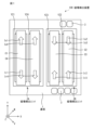
図1は、磁場検出装置100の全体構成例を表す概略平面図である。磁場検出装置100は、例えばY軸方向の磁場の変化およびZ軸方向の磁場の変化をそれぞれ検出することができる2軸磁気検出コンパスである。磁場検出装置100は、例えば地磁気を検出する電子コンパスとして用いることができる。
(Overall configuration of magnetic field detection device 100)
1 is a schematic plan view showing an example of the overall configuration of a magnetic
図1に示したように、磁場検出装置100は、例えば基板1と、磁場検出ユニット2A,2Bと、端子部3とを備えている。基板1は、X軸方向およびY軸方向に平行なXY面に沿って延在している。基板1の厚さ方向をZ軸方向とする。X軸方向、Y軸方向およびZ軸方向は、互いに直交する。磁場検出ユニット2A,2Bは、基板1のXY面の中央領域に、互いに隣り合うように設けられている。端子部3は、基板1のうちの、磁場検出ユニット2A,2Bが設けられている中央領域以外の周辺領域に設けられている。端子部3は、磁場検出ユニット2A,2Bと導通している。端子部3は、磁場検出ユニット2A,2Bと外部装置との電気的接続を可能にする電極である。
As shown in FIG. 1, the magnetic
磁場検出ユニット2Aは、素子形成領域YZ1および素子形成領域YZ4を有している。素子形成領域YZ1および素子形成領域YZ4は、例えば、それぞれY軸方向に延在すると共にX軸方向において互いに隣り合うように配置されている。素子形成領域YZ1および素子形成領域YZ4には、後述する磁気抵抗効果膜MR1,MR4が複数形成されている。磁場検出ユニット2Aは、さらに、素子形成領域YZ1とZ軸方向に重なり合うと共にY軸方向に延在する導線C1と、素子形成領域YZ4とZ軸方向に重なり合うと共にY軸方向に延在する導線C4とを有している。導線C1,C4には、+Y方向に流れるセット電流Is1,Is4がそれぞれ供給可能に構成されている。セット電流Is1,Is4は、磁気抵抗効果膜MR1,MR4にそれぞれ含まれる磁化自由層の磁化のセット動作を行うためのセット磁場を形成する。導線C1,C4には、さらに、-Y方向に流れるリセット電流Ir1,Ir4がそれぞれ供給可能に構成されている。リセット電流Ir1,Ir4は、磁気抵抗効果膜MR1,MR4にそれぞれ含まれる磁化自由層の磁化のリセット動作を行うためのリセット磁場を形成する。
The magnetic
磁場検出ユニット2Bは、素子形成領域YZ2および素子形成領域YZ3を有している。素子形成領域YZ2および素子形成領域YZ3は、例えば、それぞれY軸方向に延在すると共にX軸方向において互いに隣り合うように配置されている。素子形成領域YZ2および素子形成領域YZ3には、後述する磁気抵抗効果膜MR2,MR3が複数形成されている。磁場検出ユニット2Bは、さらに、素子形成領域YZ2とZ軸方向に重なり合うと共にY軸方向に延在する導線C2と、素子形成領域YZ3とZ軸方向に重なり合うと共にY軸方向に延在する導線C3とを有している。導線C2,C3には、-Y方向に流れるセット電流Is2,Is3がそれぞれ供給可能に構成されている。セット電流Is2,Is3は、磁気抵抗効果膜MR2,MR3にそれぞれ含まれる磁化自由層の磁化のセット動作を行うためのセット磁場を形成する。導線C2,C3には、さらに、+Y方向に流れるリセット電流Ir2,Ir3がそれぞれ供給可能に構成されている。リセット電流Ir2,Ir3は、磁気抵抗効果膜MR2,MR3にそれぞれ含まれる磁化自由層の磁化のリセット動作を行うためのリセット磁場を形成する。
The magnetic
図2は、磁場検出装置100の回路構成例を表す回路図である。
Figure 2 is a circuit diagram showing an example of the circuit configuration of the magnetic
(磁場検出装置100の回路構成)
図2に示したように、磁場検出装置100は、ブリッジ回路7L,7Rと、差分検出器8L,8Rと、演算回路9とを有している。磁場検出装置100では、それら2つのブリッジ回路7L,7Rを用いることにより、Y軸方向およびZ軸方向の磁場の変化を検出することができるようになっている。
(Circuit configuration of magnetic field detection device 100)
2, the magnetic
ブリッジ回路7Lは、4つの磁気抵抗効果素子11~14を含んでいる。ブリッジ回路7Lは、直列接続された磁気抵抗効果素子11および磁気抵抗効果素子12と、直列接続された磁気抵抗効果素子13および磁気抵抗効果素子14とが、互いに並列接続されてなるものである。より具体的には、ブリッジ回路7Lは、磁気抵抗効果素子11の一端と磁気抵抗効果素子12の一端とが接続点P1において接続され、磁気抵抗効果素子13の一端と磁気抵抗効果素子14の一端とが接続点P2において接続され、磁気抵抗効果素子11の他端と磁気抵抗効果素子14の他端とが接続点P3において接続され、磁気抵抗効果素子12の他端と磁気抵抗効果素子13の他端とが接続点P4において接続されている。ここで、接続点P3は電源Vccと接続されており、接続点P4は接地端子GNDと接続されている。接続点P1および接続点P2は、それぞれ、例えば差分検出器8Lの入力側端子と接続されている。
The
磁気抵抗効果素子11~14は、それぞれ、検出対象である信号磁場の変化を検出可能である。例えば磁気抵抗効果素子11,13は、+Y方向の信号磁場または+Z方向の信号磁場の印加により抵抗値が減少し、-Y方向の信号磁場または-Z方向の信号磁場の印加により抵抗値が増加する。一方、磁気抵抗効果素子12,14は、+Y方向の信号磁場または+Z方向の信号磁場の印加により抵抗値が増加し、-Y方向の信号磁場または-Z方向の信号磁場の印加により抵抗値が減少する。したがって、磁気抵抗効果素子11,13と磁気抵抗効果素子12,14とは、信号磁場の変化に応じて互いに例えば180°位相の異なる信号を出力する。ブリッジ回路7Lから取り出された信号は差分検出器8Lに流入する。差分検出器8Lは、接続点P3と接続点P4との間に電圧が印加されたときの接続点P1と接続点P2との間の電位差、すなわち、磁気抵抗効果素子11および磁気抵抗効果素子14のそれぞれに生ずる電圧降下の差分を検出し、差分信号SLとして演算回路9へ向けて出力する。
Each of the
ブリッジ回路7Rは、4つの磁気抵抗効果素子21~24を含んでいる。ブリッジ回路7Rは、直列接続された磁気抵抗効果素子21および磁気抵抗効果素子22と、直列接続された磁気抵抗効果素子23および磁気抵抗効果素子24とが、互いに並列接続されてなるものである。より具体的には、ブリッジ回路7Rは、磁気抵抗効果素子21の一端と磁気抵抗効果素子22の一端とが接続点P5において接続され、磁気抵抗効果素子23の一端と磁気抵抗効果素子24の一端とが接続点P6において接続され、磁気抵抗効果素子21の他端と磁気抵抗効果素子24の他端とが接続点P7において接続され、磁気抵抗効果素子22の他端と磁気抵抗効果素子23の他端とが接続点P8において接続されている。ここで、接続点P7は電源Vccと接続されており、接続点P8は接地端子GNDと接続されている。接続点P5および接続点P6は、それぞれ、例えば差分検出器8Rの入力側端子と接続されている。
The
磁気抵抗効果素子21~24は、それぞれ、検出対象である信号磁場の変化を検出可能である。例えば磁気抵抗効果素子21,23は、+Y方向の信号磁場または+Z方向の信号磁場の印加により抵抗値が減少し、-Y方向の信号磁場または-Z方向の信号磁場の印加により抵抗値が増加する。一方、磁気抵抗効果素子22,24は、+Y方向の信号磁場または+Z方向の信号磁場の印加により抵抗値が増加し、-Y方向の信号磁場または-Z方向の信号磁場の印加により抵抗値が減少する。したがって、磁気抵抗効果素子21,23と磁気抵抗効果素子22,24とは、信号磁場の変化に応じて互いに例えば180°位相の異なる信号を出力する。ブリッジ回路7Rから取り出された信号は差分検出器8Rに流入する。差分検出器8Rは、接続点P7と接続点P8との間に電圧が印加されたときの接続点P5と接続点P6との間の電位差、すなわち、磁気抵抗効果素子21および磁気抵抗効果素子24のそれぞれに生ずる電圧降下の差分を検出し、差分信号SRとして演算回路9へ向けて出力する。
Each of the
(素子形成領域YZ1~YZ4の構成)
図3は、素子形成領域YZ1~YZ4の一部を拡大して表す平面模式図である。図4は、素子形成領域YZ1~YZ4の一部を拡大して表す断面模式図である。図4は、図3に示したIV-IV線に沿った矢視方向の断面を表している。
(Configuration of element formation regions YZ1 to YZ4)
Fig. 3 is a schematic plan view showing an enlarged portion of the element formation regions YZ1 to YZ4. Fig. 4 is a schematic cross-sectional view showing an enlarged portion of the element formation regions YZ1 to YZ4. Fig. 4 shows a cross section taken along line IV-IV shown in Fig. 3.
図3および図4に示したように、素子形成領域YZ1~YZ4は、基板1と、複数の凸部4と、複数の磁気抵抗効果膜MR-Aと、複数の磁気抵抗効果膜MR-Bと、下層配線群5と、上層配線群6とを有している。下層配線群5および上層配線群6により、複数の磁気抵抗効果膜MR-Aは互いに直列接続されている。下層配線群5および上層配線群6により、複数の磁気抵抗効果膜MR-Bは互いに直列接続されている。
As shown in Figures 3 and 4, element formation regions YZ1 to YZ4 have a
基板1は、XY平面に沿って延在する平坦面1Sを有している。基板1は例えばAl2O3,SiO2,SiNなどにより形成することができる。
The
複数の凸部4は、平坦面1S上に設けられており、平坦面1Sから上方、すなわち+Z方向に突出している。複数の凸部4は、例えば酸化珪素(SiOx)などの絶縁材料により形成することができる。複数の凸部4は、例えばV軸方向にそれぞれ延在しており、W軸方向に隣り合うように配列されている。なお、図3および図4に示した例では、複数の凸部4は平坦面1S上において互いに離間して配置されている。このため、W軸方向に隣り合う2つの凸部4同士の間には、基板1の平坦面1Sが露出している。なお、V軸方向およびW軸方向は、XY面に平行であるが、X軸方向およびY軸方向の双方と非平行である。具体的には、V軸方向およびW軸方向は、例えばX軸方向およびY軸方向の双方に対して45°をなしている。さらに、V軸方向とW軸方向とは、互いに直交している。
The plurality of
複数の凸部4は、それぞれ傾斜面4Aおよび傾斜面4Bを有している。傾斜面4Aおよび傾斜面4Bは、平坦面1Sと非平行な面である。すなわち、傾斜面4Aおよび傾斜面4Bは、平坦面1Sに対して傾斜している。傾斜面4Aおよび傾斜面4Bは、V軸方向に延在する頭頂部4Tを形成し、頭頂部4Tから互いに遠ざかるにしたがって平坦面1Sに近づくように傾斜している。したがって、傾斜面4Aおよび傾斜面4Bは、互いに非平行であり、互いに傾斜しているともいえる。
なお、傾斜面4Aは本発明の「第1の傾斜面」に対応する一具体例であり、傾斜面4Bは本発明の「第2の傾斜面」に対応する一具体例である。
Each of the multiple
The
複数の磁気抵抗効果膜MR-Aは、各凸部4の傾斜面4Aに設けられている。複数の磁気抵抗効果膜MR-Aは、傾斜面4Aの長手方向であるV軸方向に沿って配列されている。複数の磁気抵抗効果膜MR-Aは、それぞれ、V軸方向を長手方向とするように延在している。同様に、複数の磁気抵抗効果膜MR-Bは、各凸部4の傾斜面4Bに設けられている。複数の磁気抵抗効果膜MR-Bは、傾斜面4Bの長手方向であるV軸方向に沿って配列されている。複数の磁気抵抗効果膜MR-Bは、それぞれ、V軸方向を長手方向とするように延在している。
なお、磁気抵抗効果膜MR-Aは本発明の「第1の磁気抵抗効果膜」に対応する一具体例であり、磁気抵抗効果膜MR-Bは本発明の「第2の磁気抵抗効果膜」に対応する一具体例である。
A plurality of magnetoresistive effect films MR-A are provided on the
The magnetoresistive film MR-A is a specific example corresponding to the "first magnetoresistive film" of the present invention, and the magnetoresistive film MR-B is a specific example corresponding to the "second magnetoresistive film" of the present invention.
下層配線群5は、磁気抵抗効果膜MR-A,MR-Bの下層、すなわち、磁気抵抗効果膜MR-Aと傾斜面4Aとの間、および磁気抵抗効果膜MR-Bと傾斜面4Bとの間にそれぞれ設けられている。下層配線群5には、下層配線51~53が複数含まれている。複数の下層配線51は、それぞれ、同じ凸部4の傾斜面4Aにおいて互いに隣り合うように設けられた2つの磁気抵抗効果膜MR-Aの下面同士を接続している。複数の下層配線52は、それぞれ、同じ凸部4の傾斜面4Bにおいて互いに隣り合うように設けられた2つの磁気抵抗効果膜MR-Bの下面同士を接続している。複数の下層配線53は、それぞれ、互いに異なる凸部4の傾斜面4Aに設けられた2つの磁気抵抗効果膜MR-Aの下面同士を接続している。
The lower wiring group 5 is provided below the magnetoresistive films MR-A and MR-B, that is, between the magnetoresistive film MR-A and the
上層配線群6は、磁気抵抗効果膜MR-A,MR-Bの上層、すなわち、磁気抵抗効果膜MR-Aから見て傾斜面4Aと反対側、および磁気抵抗効果膜MR-Bから見て傾斜面4Bと反対側にそれぞれ設けられている。上層配線群6には、上層配線61~63が複数含まれている。複数の上層配線61は、それぞれ、同じ凸部4の傾斜面4Aにおいて互いに隣り合うように設けられた2つの磁気抵抗効果膜MR-Aの上面同士を接続している。複数の上層配線62は、それぞれ、同じ凸部4の傾斜面4Bにおいて互いに隣り合うように設けられた2つの磁気抵抗効果膜MR-Bの上面同士を接続している。複数の上層配線63は、それぞれ、互いに異なる凸部4の傾斜面4Bに設けられた2つの磁気抵抗効果膜MR-Bの上面同士を接続している。
The upper layer wiring group 6 is provided on the upper layer of the magnetoresistive effect films MR-A and MR-B, that is, on the opposite side of the
このように、傾斜面4Aに設けられた複数の磁気抵抗効果膜MR-Aは、下層配線53と、上層配線61と、下層配線51とによって直列接続されて1つの磁気抵抗効果膜アレイを形成している。すなわち、磁気抵抗効果膜MR-Aは上層配線61と下層配線51との間、または、上層配線61と下層配線53との間に挟まれている。なお、複数の磁気抵抗効果膜MR-Aを含む磁気抵抗効果膜アレイの始端の下層配線53Sおよび終端の下層配線53Eは、互いに異なる端子部3にそれぞれ接続されている。
In this way, the multiple magnetoresistive films MR-A provided on the
同様に、傾斜面4Bに設けられた複数の磁気抵抗効果膜MR-Bは、上層配線63と、下層配線52と、上層配線62とによって直列接続されて1つの磁気抵抗効果膜アレイを形成している。すなわち、磁気抵抗効果膜MR-Bは上層配線63と下層配線52との間、または、上層配線62と下層配線52との間に挟まれている。なお、複数の磁気抵抗効果膜MR-Bを含む磁気抵抗効果膜アレイの始端の上層配線63Sおよび終端の上層配線63Eは、互いに異なる端子部3にそれぞれ接続されている。
Similarly, the multiple magnetoresistive films MR-B provided on the
ここで、下層配線53と上層配線63とは、傾斜面4A上および傾斜面4B上のうちの少なくとも一方で交差しており、クロスポイントXPを形成している。クロスポイントXPでは、下層配線53と上層配線63とが実質的に直交していてもよい。なお、図3に示した例では、傾斜面4Aおよび傾斜面4Bの双方にクロスポイントXPが設けられている。その一方で、下層配線53と上層配線63とは、基板1の平坦面1S上では互いに交差しないようになっている。ここでいう交差する、とは、積層方向であるZ軸方向に眺めた状態において、上層配線63が下層配線53を横切るような位置関係であることをいう。さらに、交差する、とは、下層配線53の幅方向の両端縁のうちの少なくとも一方とZ軸方向に重なり合う位置に上層配線63が設けられていることも包含する。すなわち、本実施の形態では、上層配線63と下層配線53とが並走する場合であっても、下層配線53の幅方向の端縁が、Z軸方向において上層配線63と重なり合う位置にある場合、下層配線53と上層配線63とが交差していることとなる。
Here, the
下層配線51~53および上層配線61~63は、例えばAl(アルミニウム),Cu(銅),Ag(銀)およびAu(金)、ならびにそれらを含む合金などの、高導電性非磁性金属により形成可能である。また、下層配線51~53および上層配線61~63は、いずれも、単層構造であってもよいし複数層からなる多層構造であってもよい。さらに、下層配線51~53および上層配線61~63の各々の構成材料は、互いに同一であってもよいし、互いに異なっていてもよい。 The lower wirings 51-53 and the upper wirings 61-63 can be made of highly conductive non-magnetic metals such as Al (aluminum), Cu (copper), Ag (silver), Au (gold), and alloys containing these metals. The lower wirings 51-53 and the upper wirings 61-63 may each have a single-layer structure or a multi-layer structure made up of multiple layers. Furthermore, the constituent materials of the lower wirings 51-53 and the upper wirings 61-63 may be the same as or different from each other.
素子形成領域YZ1に形成された複数の磁気抵抗効果膜MR-Aは、互いに直列接続されることにより、ブリッジ回路7Lの磁気抵抗効果素子11を構成している。また、素子形成領域YZ1に形成された複数の磁気抵抗効果膜MR-Bは、互いに直列接続されることによりブリッジ回路7Rの磁気抵抗効果素子21を構成している。
The multiple magnetoresistance effect films MR-A formed in the element formation region YZ1 are connected in series to each other to form the
素子形成領域YZ2に形成された複数の磁気抵抗効果膜MR-Aは、互いに直列接続されることにより、ブリッジ回路7Lの磁気抵抗効果素子12を構成している。また、素子形成領域YZ2に形成された複数の磁気抵抗効果膜MR-Bは、互いに直列接続されることによりブリッジ回路7Rの磁気抵抗効果素子22を構成している。
The multiple magnetoresistance effect films MR-A formed in the element formation region YZ2 are connected in series to each other to form the
素子形成領域YZ3に形成された複数の磁気抵抗効果膜MR-Aは、互いに直列接続されることにより、ブリッジ回路7Lの磁気抵抗効果素子13を構成している。また、素子形成領域YZ3に形成された複数の磁気抵抗効果膜MR-Bは、互いに直列接続されることによりブリッジ回路7Rの磁気抵抗効果素子23を構成している。
The multiple magnetoresistance effect films MR-A formed in the element formation region YZ3 are connected in series to each other to form the
素子形成領域YZ4に形成された複数の磁気抵抗効果膜MR-Aは、互いに直列接続されることにより、ブリッジ回路7Lの磁気抵抗効果素子14を構成している。また、素子形成領域YZ4に形成された複数の磁気抵抗効果膜MR-Bは、互いに直列接続されることによりブリッジ回路7Rの磁気抵抗効果素子24を構成している。
The multiple magnetoresistance effect films MR-A formed in the element formation region YZ4 are connected in series to each other to form the
なお、上述の磁場検出装置100と、X軸方向の磁場の変化を検出可能な磁場検出ユニット(便宜上、磁場検出ユニット2Cという。)とを組み合わせることにより、3軸方向の磁場の変化を検出する3軸磁気検出コンパスを実現できる。ここでいう磁場検出ユニット2Cは、例えば平坦面1Sに平行な面に複数の磁気抵抗効果膜が形成されることを除き、上記の磁場検出装置100と実質的に同じ構造を有するものを適用可能である。
In addition, by combining the above-mentioned magnetic
ここで、磁気抵抗効果素子11を構成する磁気抵抗効果膜MR-Aおよび磁気抵抗効果素子21を構成する磁気抵抗効果膜MR-B、すなわち素子形成領域YZ1に形成された磁気抵抗効果膜MR-Aおよび磁気抵抗効果膜MR-Bを包括的に磁気抵抗効果膜MR1と呼ぶこととする。また、磁気抵抗効果素子12を構成する磁気抵抗効果膜MR-Aおよび磁気抵抗効果素子22を構成する磁気抵抗効果膜MR-B、すなわち素子形成領域YZ2に形成された磁気抵抗効果膜MR-Aおよび磁気抵抗効果膜MR-Bを包括的に磁気抵抗効果膜MR2と呼ぶ。また、磁気抵抗効果素子13を構成する磁気抵抗効果膜MR-Aおよび磁気抵抗効果素子23を構成する磁気抵抗効果膜MR-B、すなわち素子形成領域YZ3に形成された磁気抵抗効果膜MR-Aおよび磁気抵抗効果膜MR-Bを包括的に磁気抵抗効果膜MR3と呼ぶ。さらに、磁気抵抗効果素子14を構成する磁気抵抗効果膜MR-Aおよび磁気抵抗効果素子24を構成する磁気抵抗効果膜MR-B、すなわち素子形成領域YZ4に形成された磁気抵抗効果膜MR-Aおよび磁気抵抗効果膜MR-Bを包括的に磁気抵抗効果膜MR4と呼ぶ。図5に、磁気抵抗効果膜MR1~MR4の積層構造の断面を模式的に表す。
Here, the magnetoresistive film MR-A constituting the
図5に示したように、磁気抵抗効果膜MR1~MR4は、磁性層を含む複数の機能膜が積層されたスピンバルブ構造を有している。具体的には、磁気抵抗効果膜MR1~MR4は、磁化固着層31と中間層32と磁化自由層33とが順に積層された積層構造を有する。磁化固着層31は、所定の方向に固着された磁化J31を有する。中間層32は非磁性体である。磁化自由層33は、信号磁場の磁束の向きに応じて磁化J33の向きが変化するようになっている。磁化固着層31、中間層32および磁化自由層33は、いずれも傾斜面4Aまたは傾斜面4Bに沿って広がる薄膜である。磁化自由層33の磁化J33の向きは、傾斜面4Aまたは傾斜面4Bに沿った面内において回転可能となっている。なお、上述したように、磁気抵抗効果膜MR1~MR4は、いずれもV軸方向に延在している。したがって、磁気抵抗効果膜MR1~MR4は、それぞれV軸方向の形状異方性を示す。このため、初期状態の磁化自由層33の磁化J33の向きは、V軸方向とほぼ平行となる。
As shown in FIG. 5, the magnetoresistive films MR1 to MR4 have a spin valve structure in which multiple functional films including a magnetic layer are stacked. Specifically, the magnetoresistive films MR1 to MR4 have a stacked structure in which a magnetization pinned
また、磁気抵抗効果膜MR1~MR4における各々の磁化J31の固着方向は、例えば図6にそれぞれ示したように設定される。図6は、磁気抵抗効果膜MR1~MR4のそれぞれについて、磁化固着層31の磁化J31の方向と、初期状態の磁化自由層33の磁化J33の方向との関係を説明するための平面模式図である。図6の(A)に示したように、磁気抵抗効果膜MR1では、例えば磁化J31の向きが+W方向であると共に磁化J33の向きが+V方向である。また、図6の(B)に示したように、磁気抵抗効果膜MR2では、例えば磁化J31の向きが-W方向であると共に磁化J33の向きが-V方向である。また、図6の(C)に示したように、磁気抵抗効果膜MR3では、例えば磁化J31の向きが+W方向であると共に磁化J33の向きが-V方向である。さらに、図6の(D)に示したように、磁気抵抗効果膜MR4では、例えば磁化J31の向きが-W方向であると共に磁化J33の向きが+V方向である。
The pinning direction of the magnetization J31 in each of the magnetoresistive films MR1 to MR4 is set, for example, as shown in FIG. 6. FIG. 6 is a schematic plan view for explaining the relationship between the direction of the magnetization J31 of the magnetization pinned
このように、磁気抵抗効果膜MR1~MR4における各々の磁化J31の固着方向は、V軸方向と直交するW軸方向とほぼ平行である。したがって、磁気抵抗効果膜MR1~MR4が信号磁場に対して高い感度を示す感度方向はW軸方向である。しかしながら、磁気抵抗効果膜MR1,MR3における磁化固着層31は+W方向に固着された磁化J31をそれぞれ有するのに対し、磁気抵抗効果膜MR2,MR4における磁化固着層31は-W方向に固着された磁化J31をそれぞれ有する。そのため、信号磁場の印加により磁気抵抗効果膜MR1,MR3の各々の抵抗値が増大する際には、磁気抵抗効果膜MR2,MR4の各々の抵抗値は減少することとなる。反対に、信号磁場の印加により磁気抵抗効果膜MR1,MR3の各々の抵抗値が減少する際には、磁気抵抗効果膜MR2,MR4の各々の抵抗値は増大する。
Thus, the pinning direction of the magnetization J31 in each of the magnetoresistive films MR1 to MR4 is approximately parallel to the W-axis direction, which is perpendicular to the V-axis direction. Therefore, the sensitivity direction in which the magnetoresistive films MR1 to MR4 are highly sensitive to the signal magnetic field is the W-axis direction. However, the magnetization pinned
なお、磁気抵抗効果膜MR1~MR4をそれぞれ構成する磁化固着層31、中間層32および磁化自由層33は、いずれも単層構造であってもよいし、複数層からなる多層構造であってもよい。
The magnetization pinned
磁化固着層31は、例えばCo(コバルト)やCoFe(コバルト鉄合金)、CoFeB(コバルト鉄ボロン合金)などの強磁性材料からなる。なお、磁気抵抗効果膜MR1~MR4において、磁化固着層31とそれぞれ隣接するように、中間層32と反対側に反強磁性層(図示せず)を設けるようにしてもよい。そのような反強磁性層は、白金マンガン合金(PtMn)やイリジウムマンガン合金(IrMn)などの反強磁性材料により構成されるものである。反強磁性層は、磁気抵抗効果膜MR1~MR4においては、+W方向のスピン磁気モーメントと-W方向のスピン磁気モーメントとが完全に打ち消し合った状態にあり、隣接する磁化固着層31の磁化J31の向きを+W方向へ固定し、あるいは-W方向へ固定するように作用する。
The magnetic pinned
中間層32は、スピンバルブ構造が磁気トンネル接合(MTJ:Magnetic Tunnel Junction)膜として機能するものである場合、例えば酸化マグネシウム(MgO)からなる非磁性のトンネルバリア層であり、量子力学に基づくトンネル電流が通過可能な程度に厚みの薄いものである。なお、中間層32は、例えばルテニウム(Ru)や金(Au)などの白金族元素や銅(Cu)などの非磁性金属により構成されていてもよい。その場合、スピンバルブ構造は巨大磁気抵抗効果(GMR:Giant Magneto Resistive effect)膜として機能する。
When the spin valve structure functions as a magnetic tunnel junction (MTJ) film, the
磁化自由層33は軟質強磁性層であり、互いに実質的に同一の材料により形成されている。磁化自由層33は、例えばCoFe、NiFeあるいはCoFeBなどによって構成される。
The magnetization
[磁場検出装置100の動作および作用]
本実施の形態の磁場検出装置100では、差分信号SLおよび差分信号SRに基づき、磁場検出装置100に印加される信号磁場の変化を演算回路9において検出することができる。
[Operation and Function of Magnetic Field Detection Device 100]
In the magnetic
(セット・リセット動作)
ところで、磁場検出装置100では、信号磁場の検出動作を行う前に、各磁気抵抗効果素子における磁化自由層の磁化を所定の方向に一旦揃えることが望ましい。より正確な信号磁場の検出動作を行うためである。具体的には、既知の大きさの外部磁場を所定の方向と、それと反対の方向とに交互に印加する。これを磁化自由層33の磁化J33のセット・リセット動作という。
(Set/Reset Operation)
Incidentally, in the magnetic
本実施の形態の磁場検出装置100では、図1に示したように導線C1~C4にそれぞれセット電流Is1~Is4を供給することでセット動作がなされる。導線C1~C4へのセット電流Is1~Is4の供給により、導線C1~C4の周囲にセット磁場がそれぞれ生成される。その結果、磁場検出ユニット2Aでは、-X方向のセット磁場を、磁気抵抗効果素子11,21の磁気抵抗効果膜MR1および磁気抵抗効果素子14,24の磁気抵抗効果膜MR4にそれぞれ印加することができる。これにより、磁気抵抗効果膜MR1,MR4における磁化自由層33の磁化J33は-X方向に向くこととなり、セット動作がなされる。一方、磁場検出ユニット2Bでは、+X方向のセット磁場を、磁気抵抗効果素子12,22の磁気抵抗効果膜MR2および磁気抵抗効果素子13,23の磁気抵抗効果膜MR3にそれぞれ印加することができる。これにより、磁気抵抗効果膜MR2,MR3における磁化自由層33の磁化J33は+X方向に向くこととなり、セット動作がなされる。
In the magnetic
また、導線C1~C4にそれぞれリセット電流Ir1~Ir4を供給することでリセット動作がなされる。導線C1~C4へのリセット電流Ir1~Ir4の供給により、導線C1~C4の周囲にリセット磁場がそれぞれ生成される。その結果、磁場検出ユニット2Aでは、+X方向のリセット磁場を磁気抵抗効果膜MR1,MR4にそれぞれ印加することができる。これにより、磁気抵抗効果膜MR1,MR4における磁化自由層33の磁化J33は+X方向に向くこととなり、リセット動作がなされる。一方、磁場検出ユニット2Bでは、-X方向のリセット磁場を磁気抵抗効果膜MR2,MR3に印加することができる。これにより、磁気抵抗効果膜MR2,MR3における磁化自由層33の磁化J33は-X方向に向くこととなりリセット動作がなされる。
Moreover, a reset operation is performed by supplying reset currents Ir1 to Ir4 to the conductors C1 to C4, respectively. By supplying the reset currents Ir1 to Ir4 to the conductors C1 to C4, a reset magnetic field is generated around the conductors C1 to C4, respectively. As a result, the magnetic
[磁場検出装置100の製造方法]
次に、図7A~7Iを参照して、磁場検出装置100の製造方法について説明する。図7A~7Iは、磁場検出装置100のうち、特に下層配線群5、磁気抵抗効果膜MR-A,MR-B、および上層配線群6の製造方法の各工程を表す断面模式図である。
[Method of manufacturing the magnetic field detection device 100]
7A to 7I, a method for manufacturing the magnetic
最初に、基板1を用意したのち、図7Aに示したように、平坦面1Sの上に、それぞれV軸方向に延在する複数の凸部4をW軸方向に並べるように形成する。そののち、基板1および複数の凸部4の全体を覆うように、導電材料膜5Zを形成する。
First, a
次に、図7Bに示したように、導電材料膜5Zを覆うように、磁気抵抗効果膜MRZを形成する。
Next, as shown in FIG. 7B, a magnetoresistive film MRZ is formed to cover the
次に、図7Cに示したように、フォトリソグラフィ法などを用いて磁気抵抗効果膜MRZを選択的にエッチングすることにより、所定形状の磁気抵抗効果膜MR-A,MR-Bを形成する。そののち、磁気抵抗効果膜MR-A,MR-Bの周囲を埋めるように絶縁膜Z1を形成する。 Next, as shown in FIG. 7C, the magnetoresistive film MRZ is selectively etched using a photolithography method or the like to form magnetoresistive films MR-A and MR-B of a predetermined shape. After that, an insulating film Z1 is formed so as to fill in the periphery of the magnetoresistive films MR-A and MR-B.
次に、図7Dに示したように、磁気抵抗効果膜MR-A,MR-Bおよび絶縁膜Z1を覆うように、第1レジスト層RS1と第2レジスト層RS2とを順次積層形成することにより2層レジストRSを形成する。 Next, as shown in FIG. 7D, a two-layer resist RS is formed by sequentially stacking a first resist layer RS1 and a second resist layer RS2 to cover the magnetoresistive films MR-A, MR-B and the insulating film Z1.
次に、図7Eに示したように、2層レジストRSを選択的に露光したのち、2層レジストRSのうち例えば露光されていない部分を洗浄により除去する。これにより、導電材料膜5Zを選択的に覆う2層レジストパターンRPを形成する。2層レジストパターンRPは、第1レジストパターンRP1と、第2レジストパターンRP2との2層構造からなる。
Next, as shown in FIG. 7E, the two-layer resist RS is selectively exposed to light, and then the unexposed portions of the two-layer resist RS are removed, for example, by cleaning. This forms a two-layer resist pattern RP that selectively covers the
次に、図7Fに示したように、2層レジストパターンRPをマスクとして用い、絶縁膜Z1および導電材料膜5Zを選択的にエッチングする。すなわち、絶縁膜Z1および導電材料膜5Zのうち、2層レジストパターンRPにより覆われていない部分を除去する。これにより、各凸部4の傾斜面4A,4Bに下層配線群5が形成される。なお、図7Fに示した断面では、各凸部4の傾斜面4Aに下層配線51がそれぞれ形成されると共に各凸部4の傾斜面4Bに下層配線52がそれぞれ形成される。そののち、絶縁膜Z1および導電材料膜5Zが除去された部分を埋めるように絶縁膜Z2を形成し、2層レジストパターンRPをリフトオフする。
Next, as shown in FIG. 7F, the insulating film Z1 and the
次に、図7Gに示したように、磁気抵抗効果膜MR-A,MR-Bの上に、2層レジストパターンRP-2を形成する。その際、2層レジストパターンRP-2のW軸方向の幅は、下層配線51,52のW軸方向の幅よりもそれぞれ狭くなるようにする。
7G, a two-layer resist pattern RP-2 is formed on the magnetoresistive films MR-A and MR-B. At this time, the width of the two-layer resist pattern RP-2 in the W-axis direction is set to be narrower than the width of the
次に、図7Hに示したように、2層レジストパターンRP-2、絶縁膜Z1、および絶縁膜Z2の全体を覆うように絶縁膜Z3を形成する。 Next, as shown in FIG. 7H, an insulating film Z3 is formed so as to cover the entire two-layer resist pattern RP-2, insulating film Z1, and insulating film Z2.
次に、2層レジストパターンRP-2を除去することにより、図7Iに示したように、絶縁膜Z3に形成された複数の開口Z3Kが表れる。複数の開口Z3Kには、磁気抵抗効果膜MR-A,MR-Bの上面が露出することとなる。 Next, the two-layer resist pattern RP-2 is removed to reveal multiple openings Z3K formed in the insulating film Z3, as shown in FIG. 7I. The upper surfaces of the magnetoresistive films MR-A and MR-B are exposed in the multiple openings Z3K.
そののち、図7Jに示したように、絶縁膜Z3に設けられた複数の開口Z3Kを埋めるように上層配線群6(図7Iでは、上層配線群6のうちの上層配線61,62を示す)を形成する。最後に、図7Kに示したように、絶縁膜Z3および上層配線群6の全体を覆うように絶縁膜Z4を形成するなどして、磁場検出装置100の製造が終了する。
7J, the upper layer wiring group 6 (upper layer wirings 61 and 62 of the upper layer wiring group 6 are shown in FIG. 7I) are formed so as to fill the multiple openings Z3K provided in the insulating film Z3. Finally, as shown in FIG. 7K, the insulating film Z4 is formed so as to entirely cover the insulating film Z3 and the upper layer wiring group 6, and the manufacturing of the magnetic
[磁場検出装置100の効果]
このように、本実施の形態の磁場検出装置100では、下層配線53と上層配線63とが傾斜面4A上および傾斜面4B上のうちの少なくとも一方で交差しており、平坦面1S上では下層配線53と上層配線63とが交差していない。すなわち、図3に示したように、クロスポイントXPが傾斜面4A上または傾斜面4B上のいずれかにあり、クロスポイントXPは平坦面1S上には存在しない。このため、下層配線53と上層配線63との短絡が生じる可能性を低減できる。これは以下に説明するように、平坦面1S上に形成される下層配線53にはバリが発生しやすいのに対し、傾斜面4A上または傾斜面4B上に形成される下層配線53にはバリが発生しにくいからである。よって、上層配線63を平坦面1S上に形成される下層配線53と交差させることなく、傾斜面4A上または傾斜面4B上に形成される下層配線53と上層配線63とが交差するようにすることで、下層配線53のバリが介在して下層配線53と上層配線63とが意図せずに導通してしまうのを回避できる。
[Effects of the magnetic field detection device 100]
Thus, in the magnetic
図8は、参考例としての磁場検出装置1000の素子形成領域を模式的に表した平面図であり、本実施の形態の図3に対応する図である。図8に示したように、参考例としての磁場検出装置1000は、基板1の平坦面1S上に形成されたクロスポイントXP1およびXP2を有している。図9Aは、図8に示したIX-IX切断線に沿った矢視方向の断面を表す断面模式図である。図9Aに示したように、クロスポイントXP1では、バリBRを介した短絡部分SHが形成されている。バリBRは、下層配線52,53のうちの、平坦面1S上の端部に発生している。このバリBRは、下層配線52,53のパターニングの際に生じるものである。図9Bは、磁場検出装置1000の製造方法の一工程を表す断面模式図であり、特に下層配線52,53の選択的エッチングを実施した直後の状態を表している。参考例の磁場検出装置1000の下層配線52,53は、本実施の形態の磁場検出装置100の下層配線群5と同様、2層レジストパターンRPを用いて導電材料膜を選択的にエッチングすることによりパターニングされる。しかしながら、参考例の磁場検出装置1000では、下層配線52,53の一部が傾斜面4A,4Bだけではなく平坦面1S上の一部をも覆うように延在している。一般に、傾斜面上に付着するレジストパターンの厚さよりも、平坦面上に付着するレジストパターンの厚さのほうが厚くなることが多い。したがって、図9Bに示したように、平坦面1S上に形成された第1レジストパターンRP1の厚さは、傾斜面4A,4B上に形成された第1レジストパターンRP1の厚さよりも厚くなることが多い。このような第1レジストパターンRP1を含む2層レジストパターンRPを用いて導電材料膜を選択的にエッチングすると、図9Bに示したように、第1レジストパターンRP1の端面に除去された導電材料膜が再付着してしまい、下層配線52,53の端面と接触したバリBRを形成することとなる。バリBRは、2層レジストパターンRPをリフトオフしたあとも残渣として平坦面1S上に残ることが多い。そののち、上層配線63を形成すると、バリBRと上層配線63とが接触した状態となる。バリBRは下層配線52,53の端面にも接触しているので、結果として上層配線63と下層配線52,53とが導通することとなってしまう。
FIG. 8 is a plan view showing a schematic representation of an element formation region of a magnetic
これに対し、本実施の形態の磁場検出装置100では、平坦面1S上にクロスポイントXPは存在しないようにしている。このため、仮にバリBRが形成されてしまったとしても、バリBRとZ軸方向に重なり合う位置に上層配線群6が設けられることはない。よって、下層配線群5と上層配線群6との短絡を回避することができる。
In contrast, in the magnetic
以上の理由から、磁場検出装置100では、短絡の発生を抑制しつつ、単位面積当たりの磁気抵抗効果素子の存在密度を向上させることができる。したがって、本実施の形態の磁場検出装置100は、動作信頼性を損なうことなく、寸法の小型化を図ることができる。
For the above reasons, the magnetic
<2.変形例>
以上、実施の形態を挙げて本発明を説明したが、本発明は上記実施の形態に限定されるものではなく、種々の変形が可能である。例えば、上記実施の形態では、4つの磁気抵抗効果素子を用いてフルブリッジ回路を形成するようにしたが、本発明では、例えば2つの磁気抵抗効果素子を用いてハーフブリッジ回路を形成するようにしてもよい。また、複数の磁気抵抗効果膜の形状および寸法は、互いに同じであってもよいし、異なっていてもよい。また、各構成要素の寸法や各構成要素のレイアウトなどは例示であってこれに限定されるものではない。
2. Modified Examples
Although the present invention has been described above with reference to the embodiments, the present invention is not limited to the above-mentioned embodiments and various modifications are possible. For example, in the above-mentioned embodiments , a full-bridge circuit is formed using four magnetoresistance effect elements, but in the present invention, for example, a half-bridge circuit may be formed using two magnetoresistance effect elements. Furthermore, the shapes and dimensions of the multiple magnetoresistance effect films may be the same as or different from each other. Furthermore, the dimensions of each component and the layout of each component are merely examples and are not limited to these.
(第1の変形例)
上記実施の形態では、例えば図3に示したように、上層配線群6と下層配線群5とがZ軸方向に重なり合う領域を、凸部4の傾斜面4A,4Bのみに設けるようにした。しかしながら、本発明は、例えば図10に示した第1の変形例としての磁場検出装置100Aをも含む概念である。図10は、本発明の第1の変形例としての磁場検出装置100Aの一部を表す概略平面図である。図10の磁場検出装置100Aでは、上層配線63と下層配線53とがZ軸方向に重なり合う領域を、凸部4が形成されていない平坦面1S上に設けるようにしている。ただし、磁場検出装置100Aでは、平坦面1S上では、上層配線63と下層配線53とが互いに交差することなく実質的に同じ方向(例えばW軸方向)へ並走するようになっている。すなわち、上層配線63は、平坦面1S上に設けられ、W軸方向に延在する平坦部63Sを含み、下層配線53は、平坦面1S上に設けられ、W軸方向に延在する平坦部53Sを含んでいる。図10に示した磁場検出装置100Aでは、平坦部53Sが、下層配線53のうちの傾斜面4Aに設けられた部分53Aと平面視で略L字状に接続されている。同様に、平坦部63Sが、上層配線63のうちの傾斜面4Bに設けられた部分63Bと平面視で略L字状に接続されている。下層配線53の平坦部53Sは、Z軸方向に重なり合うように、上層配線63の平坦部63Sと平坦面1Sとの間に設けられている。さらに、平坦面1S上に設けられた下層配線53SのV軸方向の幅W53は、それとZ軸方向に重なり合う上層配線63SのV軸方向の幅W63よりも広く、上層配線63SのV軸方向の両端縁は、下層配線53SのV軸方向の両端縁よりも内側に位置する。したがって、上層配線63は、下層配線53の両端縁とZ軸方向に重なり合う位置には存在しない。このため、仮にバリが下層配線53の平坦部53Sの両端縁に生成されたとしても、そのようなバリを介した上層配線63と下層配線53との短絡は回避できる。よって、本発明の効果が得られる。また、磁場検出装置100Aでは、傾斜面4A,4Bは、いずれも、平坦面1S上に設けられた下層配線63の平坦部63Sおよび上層配線53の平坦部53Sが延在するW軸方向に傾斜している。このため、下層配線63の平坦部63Sおよび上層配線53の平坦部53Sが斜め方向、例えばW軸方向およびV軸方向の双方と異なる方向に延在するよりも、限られた面積を効率的に利用して下層配線53および上層配線63をレイアウトすることができ、磁場検出装置100Aの小型化に寄与する。また、下層配線53および上層配線63の効率的なレイアウトにより、結果として下層配線53および上層配線63の各々の長さを短縮できる可能性がある。さらに、V軸方向に延在する傾斜面4A,4B上の下層配線51~53を形成する際のエッチング処理時の再付着物の付着を低減できる。なお、W軸方向が本発明の「第1の方向」に対応する一具体例であり、V軸方向が本発明の「第2の方向」に対応する一具体例である。さらに、平坦部53Sが本発明の「第1の平坦部」に対応する一具体例であり、平坦部63Sが本発明の「第2の平坦部」に対応する一具体例である。また、部分53Aが本発明の「第1の傾斜部」に対応する一具体例である。
(First Modification)
In the above embodiment, as shown in FIG. 3, the region where the upper layer wiring group 6 and the lower layer wiring group 5 overlap in the Z-axis direction is provided only on the
(第2の変形例)
なお、図10に示した第1の変形例としての磁場検出装置100Aでは、平坦部53Sと平坦部63Sとが互いに重なり合うようにしたが、本開示はこれに限定されるものではない。例えば図11に示した第2の変形例としての磁場検出装置100Bのように、平坦面1S上に設けられた平坦部53Sおよび平坦部63Sが、互いに重なり合うことのない位置でそれぞれW軸方向に延在していてもよい。また、図10に示した磁場検出装置100Aでは、平坦部53Sが、下層配線53のうちの傾斜面4Aに設けられた部分53Aと平面視で略L字状に接続されているが、本発明はこれに限定されるものではない。図11に示したように、平坦部53Sが、下層配線53のうちの傾斜面4Aに設けられた部分53Aと平面視で略T字状に接続されていてもよい。同様に、図10に示した磁場検出装置100Aでは、平坦部63Sが、上層配線63のうちの傾斜面4Bに設けられた部分63Bと平面視で略L字状に接続されているが、本発明はこれに限定されるものではない。図11に示したように、平坦部63Sが、上層配線63のうちの傾斜面4Bに設けられた部分63Bと平面視で略T字状に接続されていてもよい。なお、図11は、本発明の第2の変形例としての磁場検出装置100Bの一部を表す概略平面図である。図11の磁場検出装置100Bによれば、上記の構成を有することにより、下層配線53および上層配線63の効率的なレイアウトが可能となり、結果として下層配線53および上層配線63の各々の長さを短縮できる可能性がある。特に、図10に示した磁場検出装置100Aと異なり、図11の磁場検出装置100Bによれば、平坦部53Sを傾斜面4Aに設けられた部分53Aにおける延在方向(V軸方向)の端部以外の中途部分と接続できる。また、図11の磁場検出装置100Bによれば、平坦部63Sを、傾斜面4Bに設けられた部分63Bにおける延在方向(V軸方向)の端部以外の中途部分と接続できる。よって、図10に示した磁場検出装置100Aと比較して、下層配線群5および上層配線群6のレイアウトの自由度がより向上するうえ、配線抵抗の低減にも有利である。さらに、図11の磁場検出装置100Bによれば、V軸方向に延在する傾斜面4A,4B上の下層配線51~53を形成する際のエッチング処理時の再付着物の付着を低減できる。ここで、平坦部53Sの延在方向が部分53Aの延在方向に対して実質的に直交するようにするとよい。部分53Aの延在方向に対して平坦部53Sの延在方向が傾斜している場合(0°よりも大きく90°未満の場合)と比較して、再付着物の付着量をより低減できるからである。よって、下層配線53と上層配線63とが意図せずに導通してしまう可能性をより十分に低減できる。
(Second Modification)
In the magnetic field detection device 100A as the first modified example shown in FIG. 10, the flat portion 53S and the flat portion 63S are overlapped with each other, but the present disclosure is not limited to this. For example, as in the magnetic field detection device 100B as the second modified example shown in FIG. 11, the flat portion 53S and the flat portion 63S provided on the
(第3の変形例)
また、図3に示した一実施の形態の磁場検出装置100では、傾斜面4A,4Bにそれぞれ設けられた下層配線群5および上層配線群6が、複数の磁気抵抗効果膜MR-A,MR-Bを電気的に接続する導体となっている。しかしながら、本開示はこれに限定されるものではない。例えば図12および図13に示した第3の変形例としての磁場検出装置100Cのように、傾斜面4Bに、1以上のダミーパターンDBを設けるようにしてもよい。図12は、本発明の第3の変形例としての磁場検出装置100Cの一部を表す概略平面図である。また、図13は、図12に示したXIII-XIII線に沿った矢視方向の断面図である。図12および図13に示したように、傾斜面4Bに1以上のダミーパターンDBを設けることにより、W軸方向において平坦面1Sを挟んで隣り合って対向する傾斜面4Aに下層配線51,53を形成する際、下層配線51,53の端縁にバリが発生するのを抑制し、あるいは、バリが発生したとしても、その大きさを小さくすることができる。
(Third Modification)
In the magnetic
ここで、図14Aおよび図14Bに参考例として示した態様のように、W軸方向において平坦面1Sを挟んで隣り合って対向する傾斜面4Aおよび傾斜面4Bのうち、傾斜面4Aに下層配線53を形成する一方で傾斜面4Bに下層配線やダミーパターンを形成しない場合について説明する。より具体的には、図14Aおよび図14Bに示したように、W軸方向に隣り合う2つの凸部4Lおよび凸部4Rのうち、紙面左側の凸部4Lの傾斜面4Aに下層配線53および磁気抵抗効果膜MR-Aを形成し、紙面右側の凸部4Rの傾斜面4Bには下層配線および磁気抵抗効果膜を形成しない場合について説明する。この場合、まず、基板1および複数の凸部4の全体を覆う導電材料膜5Zと、磁気抵抗効果膜MR-A,MR-Bおよび絶縁膜Z1とを形成したのち、図14Aに示したように、導電材料膜5Zを選択的に覆う2層レジストパターンRPを形成する。2層レジストパターンRPは、凸部4Lの傾斜面4A,4Bに設けられる。次に、図14Bに示したように、2層レジストパターンRPをマスクとして用い、絶縁膜Z1および導電材料膜5Zを選択的にエッチングする。すなわち、絶縁膜Z1および導電材料膜5Zのうち、2層レジストパターンRPにより覆われていない部分を除去する。これにより、凸部4Lの傾斜面4Aおよび傾斜面4Bに、下層配線53および下層配線52がそれぞれ形成される。このとき、傾斜面4Aに設けられた2層レジストパターンRPの端面などには、再付着物RDが堆積する。再付着物RDは、主に、対向する凸部4Rの傾斜面4Bに形成されていた絶縁膜Z1および導電材料膜5Zがエッチングされて飛散したものである。このような再付着物は、2層レジストパターンRPをリフトオフした後であっても、凸部4Lの傾斜面4Aに形成される下層配線53の端縁にバリとして残存することがある。そのようなバリは、下層配線53の上層として形成される上層配線群6の形成を阻害したり、下層配線53と上層配線群6との意図しない短絡を発生させたりする原因となる場合がある。そこで、本変形例としての磁場検出装置100Cのように傾斜面4BにダミーパターンDBを設けることにより、ダミーパターンDBを設けた傾斜面4Bに対向する傾斜面4Aに形成される下層配線53でのバリの発生を効果的に抑制するようにしている。
Here, as shown in Fig. 14A and Fig. 14B as a reference example, a case will be described in which, of the
なお、図13に示したように、平坦面1Sに直交する高さ方向(Z軸方向)において、例えば平坦面1Sを基準としたダミーパターンDBの上端位置DBHは、平坦面1Sを基準とした下層配線53の上端位置53Hと実質的に等しいとよい。Z軸方向において、上端位置DBHと上端位置53Hとが異なる場合と比較して、下層配線53にバリが発生するのをより効果的に抑制することができるからである。
13, in the height direction (Z-axis direction) perpendicular to the
ダミーパターンDBは、例えば磁気抵抗効果膜MR-A,MR-Bなどの電子デバイスや下層配線群5および上層配線群6などの通信や電力供給を行う配線とは繋がっていない構造物である。すなわち、例えばダミーパターンDBは導電性材料によって構成されてもよいが、ダミーパターンDBは下層配線群5および上層配線群6の双方と絶縁されている。なお、ダミーパターンDBの構成材料は、例えば下層配線群5の構成材料および上層配線群6の構成材料と同じであるとよい。ダミーパターンDBを下層配線群5または上層配線群6と同時に形成可能となり、製造容易性が向上するからである。また、本変形例では、傾斜面4Bに1以上のダミーパターンDBを設けるようにしたが、本発明では実配線として利用可能な1以上のパターンを傾斜面4Bに設けるようにしてもよい。なお、その実配線として利用可能な1以上のパターンは、下層配線群5および上層配線群6の双方と絶縁された第3の配線である。すなわち、本発明の「パターン」は、実配線として利用しないダミーパターンと、実配線として利用可能なパターンとの双方を含む概念である。
The dummy pattern DB is a structure that is not connected to electronic devices such as magnetoresistive films MR-A and MR-B, or wirings for communication or power supply such as the lower layer wiring group 5 and the upper layer wiring group 6. That is, for example, the dummy pattern DB may be made of a conductive material, but the dummy pattern DB is insulated from both the lower layer wiring group 5 and the upper layer wiring group 6. The material of the dummy pattern DB may be the same as the material of the lower layer wiring group 5 and the material of the upper layer wiring group 6. This is because the dummy pattern DB can be formed simultaneously with the lower layer wiring group 5 or the upper layer wiring group 6, improving ease of manufacture. In this modification, one or more dummy patterns DB are provided on the
(第4の変形例)
さらに、本発明では、対向する2つの傾斜面の双方にダミーパターンを形成するようにしてもよい。例えば図15および図16に示した第4の変形例としての磁場検出装置100Dのように、傾斜面4Bに1以上のダミーパターンDBを設けると共に、傾斜面4Aにも1以上のダミーパターンDAを設けるようにしてもよい。図15は、本発明の第4の変形例としての磁場検出装置100Dの一部を表す概略平面図である。また、図16は、図15に示したXVI-XVI線に沿った矢視方向の断面図である。この場合、平坦面1Sに直交する高さ方向(Z軸方向)において、例えば平坦面1Sを基準としたダミーパターンDAの上端位置DAHは、平坦面1Sを基準としたダミーパターンDBの上端位置DBHと実質的に等しいとよい。
(Fourth Modification)
Furthermore, in the present invention, dummy patterns may be formed on both of the two opposing inclined surfaces. For example, as in the magnetic
磁場検出装置100Dのように、互いに対向する傾斜面4Aおよび傾斜面4Bの双方にダミーパターンDAおよびダミーパターンDBをそれぞれ設けるようにすることで、下層配線群5を形成する際に平坦面1Sおよび凸部4を覆うように形成されるレジストパターンの分布密度を均質化することができる。すなわち、平坦面1Sおよび凸部4を覆うレジストパターンが高密度で形成される領域と、平坦面1Sおよび凸部4を覆うレジストパターンが低密度で形成される領域との密度差を低減することができる。その結果、露光や現像を行う際のレジストパターンの寸法や形状をより高い精度で制御できる。よって、そのレジストパターンを用いて形成される下層配線群5の寸法のばらつきを低減できる。また、隣り合う2つの凸部4の間に挟まれた領域の平坦面1Sを横断するように形成される下層配線53を形成する場合に、傾斜面4Aもしくは傾斜面4Bから受ける露光ハレーションの影響を低減することができる。そのような傾斜面4Aもしくは傾斜面4Bからの露光ハレーションがあると、下層配線53をパターニングするためのレジストパターンの形状が崩れる場合があり、その場合、下層配線53の寸法精度が低下する可能性がある。よって、磁場検出装置100Dのように、互いに対向する傾斜面4Aおよび傾斜面4Bの双方にダミーパターンDAおよびダミーパターンDBをそれぞれ設けることで、露光時のハレーションを低減させ、下層配線53の寸法精度の低下を防ぐことができる。また、本変形例では、傾斜面4Aに1以上のダミーパターンDAを設けると共に傾斜面4Bに1以上のダミーパターンDBを設けるようにしたが、本発明では実配線として利用可能な1以上のパターンを傾斜面4A,4Bにそれぞれ設けるようにしてもよい。なお、その実配線として利用可能な1以上のパターンは、下層配線群5および上層配線群6の双方と絶縁された第3の配線である。すなわち、本発明の「パターン」は、実配線として利用しないダミーパターンと、実配線として利用可能なパターンとの双方を含む概念である。
As in the magnetic
また、図3に示した平面模式図では、各凸部4の平面形状がV軸方向を長手方向とする矩形状となっているが、本実施の形態の凸部4の平面形状はこれに限定されるものではない。凸部4は、例えば長手方向の両端部がそれぞれ半円形状であるレーストラック形状の輪郭を有していてもよい。また、図4では、傾斜面4A,4Bがいずれも平面である場合を例示したが、傾斜面4A,4Bはいずれも湾曲した面であってもよい。また、図4に示した例では、頭頂部4Tが傾斜面4Aと傾斜面4Bとが交差する角の頂点となっているが、頭頂部4Tはラウンド形状の断面を有するものであってもよい。
In the schematic plan view shown in FIG. 3, the planar shape of each
100…磁場検出装置、1…基板、2A,2B…磁場検出ユニット、3…端子部、4…凸部、40…頭頂部、41,42…傾斜面、5…下部配線群、51~53…下部配線、6…上部配線群、61~63…上部配線、31…磁化固着層、32…中間層、33…磁化自由層、7L,7R…ブリッジ回路、8L,8R…差分検出器、9…演算回路、DA,DB…ダミーパターン、Is1~Is4…セット電流、Ir1~Ir4…リセット電流、MR1~MR4…磁気抵抗効果膜、YZ1~YZ4…素子形成領域。 100...magnetic field detection device, 1...substrate, 2A, 2B...magnetic field detection unit, 3...terminal portion, 4...convex portion, 40...top portion, 41, 42...inclined surface, 5...lower wiring group, 51-53...lower wiring, 6...upper wiring group, 61-63...upper wiring, 31...magnetic pinned layer, 32...intermediate layer, 33...magnetic free layer, 7L, 7R...bridge circuit, 8L, 8R...differential detector, 9...arithmetic circuit, DA, DB...dummy pattern, Is1-Is4...set current, Ir1-Ir4...reset current, MR1-MR4...magnetoresistive film, YZ1-YZ4...element formation region.
Claims (12)
前記平坦面に対して傾斜した第1の傾斜面と、前記平坦面および前記第1の傾斜面の双方に対して傾斜した第2の傾斜面とをそれぞれ含み、前記平坦面にそれぞれ設けられた第1の凸部および第2の凸部と、
前記第1の傾斜面に設けられた第1の磁気抵抗効果膜と、
前記第2の傾斜面に設けられた第2の磁気抵抗効果膜と、
前記第1の凸部の前記第1の傾斜面に設けられた前記第1の磁気抵抗効果膜と、前記第2の凸部の前記第1の傾斜面に設けられた前記第1の磁気抵抗効果膜とを繋ぐ第1の配線と、
前記第1の凸部の前記第2の傾斜面に設けられた前記第2の磁気抵抗効果膜と、前記第2の凸部の前記第2の傾斜面に設けられた前記第2の磁気抵抗効果膜とを繋ぐ第2の配線と
を有し、
前記第1の配線と前記第2の配線とが、前記第1の傾斜面上および前記第2の傾斜面上のうちの少なくとも一方で交差している
磁場検出装置。 a substrate including a planar surface;
a first inclined surface inclined with respect to the flat surface, and a second inclined surface inclined with respect to both the flat surface and the first inclined surface, a first convex portion and a second convex portion provided on the flat surface;
a first magnetoresistive film provided on the first inclined surface;
a second magnetoresistive film provided on the second inclined surface;
a first wiring connecting the first magnetoresistance effect film provided on the first inclined surface of the first convex portion and the first magnetoresistance effect film provided on the first inclined surface of the second convex portion;
the second magnetoresistance effect film provided on the second inclined surface of the first convex portion and a second wiring connecting the second magnetoresistance effect film provided on the second inclined surface of the second convex portion,
A magnetic field detection device, wherein the first wiring and the second wiring cross each other on at least one of the first inclined surface and the second inclined surface.
前記第1の配線と前記第2の配線とが、前記平坦面上で交差することなく、前記第1の傾斜面上および前記第2の傾斜面上のうちの少なくとも一方で交差している
請求項1記載の磁場検出装置。 the first convex portion and the second convex portion are disposed apart from each other on the flat surface,
The magnetic field detection device according to claim 1 , wherein the first wiring and the second wiring do not cross each other on the flat surface, but cross each other on at least one of the first inclined surface and the second inclined surface.
前記平坦面に対して傾斜した第1の傾斜面と、前記平坦面および前記第1の傾斜面の双方に対して傾斜した第2の傾斜面とをそれぞれ含み、前記平坦面にそれぞれ設けられた第1から第3の凸部と、a first inclined surface inclined with respect to the flat surface, and a second inclined surface inclined with respect to both the flat surface and the first inclined surface; and first to third convex portions provided on the flat surface;
前記第1から第3の凸部のそれぞれの前記第1の傾斜面に設けられた第1の磁気抵抗効果膜と、a first magnetoresistance effect film provided on the first inclined surface of each of the first to third convex portions;
前記第1から第3の凸部のそれぞれの前記第2の傾斜面に設けられた第2の磁気抵抗効果膜と、a second magnetoresistance effect film provided on the second inclined surface of each of the first to third convex portions;
前記第1の凸部の前記第1の傾斜面に設けられた前記第1の磁気抵抗効果膜と、前記第2の凸部の前記第1の傾斜面に設けられた前記第1の磁気抵抗効果膜とを繋ぐ第1の配線と、a first wiring connecting the first magnetoresistance effect film provided on the first inclined surface of the first convex portion and the first magnetoresistance effect film provided on the first inclined surface of the second convex portion;
前記第1の凸部の前記第2の傾斜面に設けられた前記第2の磁気抵抗効果膜と、前記第3の凸部の前記第2の傾斜面に設けられた前記第2の磁気抵抗効果膜とを繋ぐ第2の配線とa second wiring that connects the second magnetoresistance effect film provided on the second inclined surface of the first convex portion and the second magnetoresistance effect film provided on the second inclined surface of the third convex portion;
を有し、having
前記第1の配線と前記第2の配線とが、前記第1の凸部の前記第1の傾斜面上および前記第1の凸部の前記第2の傾斜面上のうちの少なくとも一方で交差しているThe first wiring and the second wiring intersect at least one of the first inclined surface of the first protrusion and the second inclined surface of the first protrusion.
磁場検出装置。Magnetic field detection device.
前記第1の配線と前記第2の配線とが、前記平坦面上で交差することなく、前記第1の凸部の前記第1の傾斜面上および前記第1の凸部の前記第2の傾斜面上のうちの少なくとも一方で交差しているThe first wiring and the second wiring do not intersect on the flat surface, but intersect at least one of the first inclined surface of the first convex portion and the second inclined surface of the first convex portion.
請求項3記載の磁場検出装置。4. The magnetic field detection device according to claim 3.
請求項1から請求項4のいずれか1項に記載の磁場検出装置。 The magnetic field detection device according to claim 1 , wherein the first wiring and the second wiring are substantially perpendicular to each other.
前記第2の配線は、前記平坦面に設けられて前記第1の方向に延在する第2の平坦部を含み、
前記第1の平坦部は、前記第2の平坦部と前記平坦面との間に設けられ、
前記第1の方向と直交すると共に前記平坦面に平行な第2の方向において、前記第1の平坦部の幅は前記第2の平坦部の幅よりも広く、
前記第2の平坦部における前記第2の方向の両端縁は、前記第1の平坦部における前記第2の方向の両端縁よりも内側に位置する
請求項1から請求項4のいずれか1項に記載の磁場検出装置。 the first wiring includes a first flat portion provided on the flat surface and extending in a first direction;
the second wiring includes a second flat portion provided on the flat surface and extending in the first direction;
The first flat portion is provided between the second flat portion and the flat surface,
In a second direction perpendicular to the first direction and parallel to the flat surface, a width of the first flat portion is wider than a width of the second flat portion;
The magnetic field detection device according to claim 1 , wherein both end edges of the second flat portion in the second direction are located more inward than both end edges of the first flat portion in the second direction.
請求項6記載の磁場検出装置。 The magnetic field detection device according to claim 6 , wherein the first inclined surface and the second inclined surface are both inclined in the first direction.
請求項7記載の磁場検出装置。 The magnetic field detection device according to claim 7 , wherein the first flat portion includes protrusions extending in a thickness direction perpendicular to the flat surface near both end edges in the second direction.
前記第2の配線は、前記第1の凸部の前記第2の傾斜面に設けられた前記第2の磁気抵抗効果膜の上面と、前記第2の凸部の前記第2の傾斜面に設けられた前記第2の磁気抵抗効果膜の上面とを繋いでいる
請求項1または請求項2に記載の磁場検出装置。 the first wiring connects a lower surface of the first magnetoresistive film provided on the first inclined surface of the first convex portion to a lower surface of the first magnetoresistive film provided on the first inclined surface of the second convex portion;
The magnetic field detection device described in claim 1 or claim 2, wherein the second wiring connects an upper surface of the second magnetoresistive effect film provided on the second inclined surface of the first convex portion to an upper surface of the second magnetoresistive effect film provided on the second inclined surface of the second convex portion .
前記第2の配線は、前記第1の凸部の前記第2の傾斜面に設けられた前記第2の磁気抵抗効果膜の上面と、前記第3の凸部の前記第2の傾斜面に設けられた前記第2の磁気抵抗効果膜の上面とを繋いでいるThe second wiring connects an upper surface of the second magnetoresistance effect film provided on the second inclined surface of the first convex portion and an upper surface of the second magnetoresistance effect film provided on the second inclined surface of the third convex portion.
請求項3または請求項4に記載の磁場検出装置。The magnetic field detection device according to claim 3 or 4.
前記第1の平坦部は、前記第2の方向における前記第1の傾斜部の中途部分と接続されている
請求項1から請求項10のいずれか1項に記載の磁場検出装置。 the first wiring includes a first flat portion provided on the flat surface and extending in a first direction, and a first inclined portion provided on the first inclined surface or the second inclined surface and extending in a second direction;
The magnetic field detection device according to claim 1 , wherein the first flat portion is connected to a middle portion of the first inclined portion in the second direction.
請求項11記載の磁場検出装置。 The magnetic field detection device according to claim 11 , wherein the first direction and the second direction are substantially perpendicular to each other.
Priority Applications (6)
| Application Number | Priority Date | Filing Date | Title |
|---|---|---|---|
| JP2022032603A JP2023046216A (en) | 2021-09-22 | 2022-03-03 | Magnetic field detector |
| US17/946,838 US12072397B2 (en) | 2021-09-22 | 2022-09-16 | Magnetic field detection apparatus |
| US17/946,817 US20230092757A1 (en) | 2021-09-22 | 2022-09-16 | Magnetic field detection apparatus |
| CN202211157122.2A CN115902723A (en) | 2021-09-22 | 2022-09-22 | Magnetic field detection device |
| CN202211157092.5A CN115902722A (en) | 2021-09-22 | 2022-09-22 | Magnetic field detection device |
| US18/775,761 US20240369651A1 (en) | 2021-09-22 | 2024-07-17 | Magnetic field detection apparatus |
Applications Claiming Priority (2)
| Application Number | Priority Date | Filing Date | Title |
|---|---|---|---|
| JP2021154816 | 2021-09-22 | ||
| JP2021154816 | 2021-09-22 |
Related Child Applications (1)
| Application Number | Title | Priority Date | Filing Date |
|---|---|---|---|
| JP2022032603A Division JP2023046216A (en) | 2021-09-22 | 2022-03-03 | Magnetic field detector |
Publications (2)
| Publication Number | Publication Date |
|---|---|
| JP2023046203A JP2023046203A (en) | 2023-04-03 |
| JP7488840B2 true JP7488840B2 (en) | 2024-05-22 |
Family
ID=85777187
Family Applications (1)
| Application Number | Title | Priority Date | Filing Date |
|---|---|---|---|
| JP2022009846A Active JP7488840B2 (en) | 2021-09-22 | 2022-01-26 | Magnetic Field Detection Device |
Country Status (1)
| Country | Link |
|---|---|
| JP (1) | JP7488840B2 (en) |
Citations (6)
| Publication number | Priority date | Publication date | Assignee | Title |
|---|---|---|---|---|
| US20050270020A1 (en) | 2004-06-03 | 2005-12-08 | Honeywell International Inc. | Integrated three-dimensional magnetic sensing device and method to fabricate an integrated three-dimensional magnetic sensing device |
| JP2006278439A (en) | 2005-03-28 | 2006-10-12 | Yamaha Corp | Method for manufacturing magnetic sensor |
| JP2007212275A (en) | 2006-02-09 | 2007-08-23 | Yamaha Corp | Triaxial magnetic sensor and manufacturing method thereof |
| JP2009020092A (en) | 2007-06-13 | 2009-01-29 | Ricoh Co Ltd | Magnetic sensor and method of manufacturing the same |
| JP2015532429A (en) | 2012-10-12 | 2015-11-09 | メムシック, インコーポレイテッドMemsic, Inc. | Monolithic 3-axis magnetic field sensor |
| JP2021092527A (en) | 2019-12-11 | 2021-06-17 | Tdk株式会社 | Magnetic field detector and current detector |
-
2022
- 2022-01-26 JP JP2022009846A patent/JP7488840B2/en active Active
Patent Citations (6)
| Publication number | Priority date | Publication date | Assignee | Title |
|---|---|---|---|---|
| US20050270020A1 (en) | 2004-06-03 | 2005-12-08 | Honeywell International Inc. | Integrated three-dimensional magnetic sensing device and method to fabricate an integrated three-dimensional magnetic sensing device |
| JP2006278439A (en) | 2005-03-28 | 2006-10-12 | Yamaha Corp | Method for manufacturing magnetic sensor |
| JP2007212275A (en) | 2006-02-09 | 2007-08-23 | Yamaha Corp | Triaxial magnetic sensor and manufacturing method thereof |
| JP2009020092A (en) | 2007-06-13 | 2009-01-29 | Ricoh Co Ltd | Magnetic sensor and method of manufacturing the same |
| JP2015532429A (en) | 2012-10-12 | 2015-11-09 | メムシック, インコーポレイテッドMemsic, Inc. | Monolithic 3-axis magnetic field sensor |
| JP2021092527A (en) | 2019-12-11 | 2021-06-17 | Tdk株式会社 | Magnetic field detector and current detector |
Also Published As
| Publication number | Publication date |
|---|---|
| JP2023046203A (en) | 2023-04-03 |
Similar Documents
| Publication | Publication Date | Title |
|---|---|---|
| US11024799B2 (en) | Methods of manufacturing a magnetic field sensor | |
| US7054114B2 (en) | Two-axis magnetic field sensor | |
| US7687284B2 (en) | Magnetic sensor and manufacturing method therefor | |
| US11994566B2 (en) | Magnetic sensor and its manufacturing method | |
| US20110089941A1 (en) | Magnetic sensor and magnetic sensor module | |
| JP7106591B2 (en) | Magnetic field detector and current detector | |
| JP7024810B2 (en) | Magnetic field detector and current detector | |
| JP7024811B2 (en) | Magnetic field detector and current detector | |
| US12072397B2 (en) | Magnetic field detection apparatus | |
| JP7488840B2 (en) | Magnetic Field Detection Device | |
| JP2010256366A (en) | Magnetic sensor and method of manufacturing the same | |
| JP2023046216A (en) | Magnetic field detector | |
| US20240369651A1 (en) | Magnetic field detection apparatus | |
| WO2010137606A1 (en) | Magnetic sensor | |
| CN116148731A (en) | Magnetic sensor and manufacturing method thereof | |
| JP7327597B2 (en) | Magnetic field detector and current detector | |
| CN119414311A (en) | TMR magnetic sensor and preparation method thereof | |
| US12105163B2 (en) | Magnetic sensor | |
| JP2008309633A (en) | Magnetic sensor |
Legal Events
| Date | Code | Title | Description |
|---|---|---|---|
| A521 | Request for written amendment filed |
Free format text: JAPANESE INTERMEDIATE CODE: A523 Effective date: 20220530 |
|
| A521 | Request for written amendment filed |
Free format text: JAPANESE INTERMEDIATE CODE: A523 Effective date: 20221014 |
|
| A621 | Written request for application examination |
Free format text: JAPANESE INTERMEDIATE CODE: A621 Effective date: 20230711 |
|
| A977 | Report on retrieval |
Free format text: JAPANESE INTERMEDIATE CODE: A971007 Effective date: 20240213 |
|
| A131 | Notification of reasons for refusal |
Free format text: JAPANESE INTERMEDIATE CODE: A131 Effective date: 20240220 |
|
| A521 | Request for written amendment filed |
Free format text: JAPANESE INTERMEDIATE CODE: A523 Effective date: 20240229 |
|
| TRDD | Decision of grant or rejection written | ||
| A01 | Written decision to grant a patent or to grant a registration (utility model) |
Free format text: JAPANESE INTERMEDIATE CODE: A01 Effective date: 20240430 |
|
| A61 | First payment of annual fees (during grant procedure) |
Free format text: JAPANESE INTERMEDIATE CODE: A61 Effective date: 20240510 |
|
| R150 | Certificate of patent or registration of utility model |
Ref document number: 7488840 Country of ref document: JP Free format text: JAPANESE INTERMEDIATE CODE: R150 |