JP7447016B2 - Systems and methods for characterizing semiconductor devices - Google Patents
Systems and methods for characterizing semiconductor devices Download PDFInfo
- Publication number
- JP7447016B2 JP7447016B2 JP2020560412A JP2020560412A JP7447016B2 JP 7447016 B2 JP7447016 B2 JP 7447016B2 JP 2020560412 A JP2020560412 A JP 2020560412A JP 2020560412 A JP2020560412 A JP 2020560412A JP 7447016 B2 JP7447016 B2 JP 7447016B2
- Authority
- JP
- Japan
- Prior art keywords
- shg
- sample
- region
- signal
- light
- Prior art date
- Legal status (The legal status is an assumption and is not a legal conclusion. Google has not performed a legal analysis and makes no representation as to the accuracy of the status listed.)
- Active
Links
Images


Classifications
-
- G—PHYSICS
- G01—MEASURING; TESTING
- G01R—MEASURING ELECTRIC VARIABLES; MEASURING MAGNETIC VARIABLES
- G01R31/00—Arrangements for testing electric properties; Arrangements for locating electric faults; Arrangements for electrical testing characterised by what is being tested not provided for elsewhere
- G01R31/26—Testing of individual semiconductor devices
- G01R31/265—Contactless testing
- G01R31/2656—Contactless testing using non-ionising electromagnetic radiation, e.g. optical radiation
-
- G—PHYSICS
- G01—MEASURING; TESTING
- G01N—INVESTIGATING OR ANALYSING MATERIALS BY DETERMINING THEIR CHEMICAL OR PHYSICAL PROPERTIES
- G01N21/00—Investigating or analysing materials by the use of optical means, i.e. using sub-millimetre waves, infrared, visible or ultraviolet light
- G01N21/62—Systems in which the material investigated is excited whereby it emits light or causes a change in wavelength of the incident light
- G01N21/63—Systems in which the material investigated is excited whereby it emits light or causes a change in wavelength of the incident light optically excited
- G01N21/636—Systems in which the material investigated is excited whereby it emits light or causes a change in wavelength of the incident light optically excited using an arrangement of pump beam and probe beam; using the measurement of optical non-linear properties
-
- G—PHYSICS
- G01—MEASURING; TESTING
- G01N—INVESTIGATING OR ANALYSING MATERIALS BY DETERMINING THEIR CHEMICAL OR PHYSICAL PROPERTIES
- G01N21/00—Investigating or analysing materials by the use of optical means, i.e. using sub-millimetre waves, infrared, visible or ultraviolet light
- G01N21/84—Systems specially adapted for particular applications
- G01N21/88—Investigating the presence of flaws or contamination
- G01N21/95—Investigating the presence of flaws or contamination characterised by the material or shape of the object to be examined
- G01N21/9501—Semiconductor wafers
- G01N21/9505—Wafer internal defects, e.g. microcracks
-
- G—PHYSICS
- G01—MEASURING; TESTING
- G01R—MEASURING ELECTRIC VARIABLES; MEASURING MAGNETIC VARIABLES
- G01R31/00—Arrangements for testing electric properties; Arrangements for locating electric faults; Arrangements for electrical testing characterised by what is being tested not provided for elsewhere
- G01R31/26—Testing of individual semiconductor devices
- G01R31/2601—Apparatus or methods therefor
-
- H—ELECTRICITY
- H10—SEMICONDUCTOR DEVICES; ELECTRIC SOLID-STATE DEVICES NOT OTHERWISE PROVIDED FOR
- H10D—INORGANIC ELECTRIC SEMICONDUCTOR DEVICES
- H10D84/00—Integrated devices formed in or on semiconductor substrates that comprise only semiconducting layers, e.g. on Si wafers or on GaAs-on-Si wafers
- H10D84/40—Integrated devices formed in or on semiconductor substrates that comprise only semiconducting layers, e.g. on Si wafers or on GaAs-on-Si wafers characterised by the integration of at least one component covered by groups H10D12/00 or H10D30/00 with at least one component covered by groups H10D10/00 or H10D18/00, e.g. integration of IGFETs with BJTs
-
- H10P74/203—
-
- H10P74/27—
-
- H10P74/277—
-
- G—PHYSICS
- G01—MEASURING; TESTING
- G01N—INVESTIGATING OR ANALYSING MATERIALS BY DETERMINING THEIR CHEMICAL OR PHYSICAL PROPERTIES
- G01N21/00—Investigating or analysing materials by the use of optical means, i.e. using sub-millimetre waves, infrared, visible or ultraviolet light
- G01N21/84—Systems specially adapted for particular applications
- G01N21/8422—Investigating thin films, e.g. matrix isolation method
- G01N2021/8438—Mutilayers
-
- G—PHYSICS
- G01—MEASURING; TESTING
- G01N—INVESTIGATING OR ANALYSING MATERIALS BY DETERMINING THEIR CHEMICAL OR PHYSICAL PROPERTIES
- G01N21/00—Investigating or analysing materials by the use of optical means, i.e. using sub-millimetre waves, infrared, visible or ultraviolet light
- G01N21/84—Systems specially adapted for particular applications
- G01N2021/8461—Investigating impurities in semiconductor, e.g. Silicon
-
- H—ELECTRICITY
- H10—SEMICONDUCTOR DEVICES; ELECTRIC SOLID-STATE DEVICES NOT OTHERWISE PROVIDED FOR
- H10D—INORGANIC ELECTRIC SEMICONDUCTOR DEVICES
- H10D84/00—Integrated devices formed in or on semiconductor substrates that comprise only semiconducting layers, e.g. on Si wafers or on GaAs-on-Si wafers
- H10D84/80—Integrated devices formed in or on semiconductor substrates that comprise only semiconducting layers, e.g. on Si wafers or on GaAs-on-Si wafers characterised by the integration of at least one component covered by groups H10D12/00 or H10D30/00, e.g. integration of IGFETs
Landscapes
- Physics & Mathematics (AREA)
- General Physics & Mathematics (AREA)
- Health & Medical Sciences (AREA)
- General Health & Medical Sciences (AREA)
- Analytical Chemistry (AREA)
- Biochemistry (AREA)
- Chemical & Material Sciences (AREA)
- Immunology (AREA)
- Pathology (AREA)
- Life Sciences & Earth Sciences (AREA)
- Engineering & Computer Science (AREA)
- Manufacturing & Machinery (AREA)
- Toxicology (AREA)
- Electromagnetism (AREA)
- Nuclear Medicine, Radiotherapy & Molecular Imaging (AREA)
- Optics & Photonics (AREA)
- Nonlinear Science (AREA)
- Testing Or Measuring Of Semiconductors Or The Like (AREA)
- Computer Hardware Design (AREA)
- Microelectronics & Electronic Packaging (AREA)
- Power Engineering (AREA)
- Automation & Control Theory (AREA)
- Investigating Or Analysing Materials By Optical Means (AREA)
- Investigating Materials By The Use Of Optical Means Adapted For Particular Applications (AREA)
Description
(関連する出願への相互参照)
本出願は、35 USC §119(e)の優先権の利益に基づいて、2018年4月27日出願の米国仮特許出願第62/663942号「光第二高調波発生によるパターン化されたウエハを評価する方法」、2018年4月27日出願の米国仮出願第62/663925号「SHG測定による界面電気的特性のためのパラメトリックモデリング」、および2018年4月27日出願の米国仮出願第62/663924号「光第二高調波発生によるプロセス誘導充電の検出のためのテスト構造設計」を援用する。
(Cross reference to related applications)
This application is filed with the benefit of priority at 35 USC §119(e) and is filed under U.S. Provisional Patent Application No. 62/663,942 filed April 27, 2018, entitled "Patterned Wafers by Optical Second Harmonic Generation". ”, U.S. Provisional Application No. 62/663,925, “Parametric Modeling for Interfacial Electrical Properties by SHG Measurements,” filed April 27, 2018, and U.S. Provisional Application No. 62/663,925, filed April 27, 2018 No. 62/663,924 "Test Structure Design for Detection of Process Induced Charging by Optical Second Harmonic Generation" is incorporated herein by reference.
本出願の対象は、第二高調波発生(SHG)に基づくウエハ検査、半導体計測学、物質特性評価、表面特性評価および/または界面分析のためのシステムに関する。 The subject matter of the present application relates to systems for wafer inspection, semiconductor metrology, material characterization, surface characterization and/or interface analysis based on second harmonic generation (SHG).
非線形光学において、光ビーム入力は、それらの入力の和、差、または高調波周波数として出力される。第二高調波発生(SHG)は、光がある角度で入射光源の光ビームの二倍の周波数でもって物質から放出される非線形効果である。このプロセスは、入射放射のエネルギーEの二つの光子を組み合わせて、エネルギー2Eの単一の光子を生成する(つまり、周波数が2倍(2ω)または波長が半分の光を生成する)ものと見なすことができる。 In nonlinear optics, optical beam inputs are output as the sum, difference, or harmonic frequencies of those inputs. Second harmonic generation (SHG) is a nonlinear effect in which light is emitted from a material at a certain angle with twice the frequency of the incident source light beam. This process considers the combination of two photons of energy E of the incident radiation to produce a single photon of energy 2E (i.e., producing light with twice the frequency (2ω) or half the wavelength). be able to.
SHG技術を使用した科学的研究の調査は、T.F.ハインツ等著、「半導体表面からの光第二高調波発生」、レーザ研究の進歩III(A.C.タム、J.L.コール、W.C.スチュワレー編、米国物理学会、ニューヨーク、1988)所収、p.452によって提供された。そこに見られるように、SHGプロセスは、対称中心を示す物質(つまり、反転または中心対称物質)のバルク内では発生しない。これらの物質の場合、SHGプロセスは、バルク物質の反転対称性が破られている表面および/または界面でのみ認識できる。そのため、SHGプロセスは、表面および界面の特性に対して独自の感度を提供する。 A survey of scientific research using SHG technology is provided by T. F. Heinz et al., "Optical Second Harmonic Generation from Semiconductor Surfaces", Advances in Laser Research III (eds. A.C. Tam, J.L. Cole, and W.C. Stewart), American Physical Society, New York, 1988. Collection, p. Provided by 452. As seen there, the SHG process does not occur within the bulk of materials exhibiting centers of symmetry (i.e., inversion or centrosymmetric materials). For these materials, SHG processes are only discernible at surfaces and/or interfaces where the inversion symmetry of the bulk material is broken. As such, the SHG process offers unique sensitivity to surface and interfacial properties.
同様の理解について、SHG効果が、ハインツ等の米国特許第5294289号明細書に記載されている。ダウナー等の米国特許第5557409号、ハントの米国特許第6795175号、第6781686号、第6788405号、第6819844号、第6882414号、および第7304305号、トーク等の第6856159号、アレス等の第7158284号明細書のそれぞれは、また、採用する可能性のある他の手法または「ツール」について説明する。しかし、これらの特許の教示によっても、半導体製造および計測用の確立した技術として、SHGを採用する際の主な障害のいくつかは克服されないように思える。 A similar understanding of the SHG effect is described in US Pat. No. 5,294,289 to Heinz et al. U.S. Pat. No. 5,557,409 to Downer et al., U.S. Pat. No. 6,795,175, U.S. Pat. Each of the patent specifications also describes other techniques or "tools" that may be employed. However, even the teachings of these patents do not appear to overcome some of the major obstacles to the adoption of SHG as an established technology for semiconductor manufacturing and metrology.
(第I部)
半導体基板層内の電子が、和の周波数発生(SFG)のための異なる電力特性を有する各ポンプ光源およびプローブ光源によって種々に励起されるSHG計測ツールについて記載する(例えば、通常はSHG)。そのような手法について、積層半導体装置テンプレートにおける異種界面に電位差を誘導して「ポンプ」として動作する「追加の」集積光源(例えば、紫外線フラッシュランプまたはレーザ)を、「プローブ」光源として動作する短パルスまたは超短パルスレーザ(例えば、フェムト秒固体レーザ)とともに備える、計測特性評価ツールを提供する。効用は、単一のレーザSHG、もしくは二重または複数のレーザSFGシステムからはっきり区別されるように、異なる目的のための二つの異なる源を一斉にまたは互いに連動させて(後述する、様々な時間オフセットおよび/または可変ポンプエネルギー方法を介して)使用することから生じる。
(Part I)
A SHG metrology tool is described in which electrons in a semiconductor substrate layer are excited differently by each pump and probe source having different power characteristics for sum frequency generation (SFG) (eg, typically SHG). For such approaches, an "additional" integrated light source (e.g., an ultraviolet flashlamp or laser) acts as a "pump" by inducing a potential difference across dissimilar interfaces in the stacked semiconductor device template, and a shorter integrated light source (e.g., an ultraviolet flash lamp or laser) acts as a "probe" light source. A metrology characterization tool is provided for use with pulsed or ultrashort pulsed lasers (e.g., femtosecond solid state lasers). The utility is to provide two different sources for different purposes in unison or in conjunction with each other (at various times, as discussed below), as distinct from single laser SHG or dual or multiple laser SFG systems. via offset and/or variable pump energy methods).
一方法では、ポンプについて、いくつかの物質の総特性評価時間を低減することを可能にする前励起または予備励起光源として使用する。そのような多くの実装では、時間依存電場を、プローブ/プローブレーザによって一次生成していない。この方法の一変形では、ポンプにより、ウエハ全体をUVで照らし、次いでプローブレーザを使って、そのウエハ全体もしくは一部について一点当たり最小プローブ時間を費やしながらラスターするか、またはそうでなければスキャンする(例えば、ハードウェアがレーザを動かせる速度でスキャンする)。この点に関する選択肢には、ウエハ移動により、(スキャン)列に沿ったステップで、行ごとにスキャンを行うことが含まれる。別の手法では、ウエハを半径に沿って回転させスキャンすることもできる。 In one method, the pump is used as a pre-excitation or pre-excitation light source, which makes it possible to reduce the total characterization time of some materials. In many such implementations, the time-dependent electric field is not primarily generated by a probe/probe laser. In one variation of this method, the entire wafer is illuminated with UV light by a pump and then rastered or otherwise scanned using a probe laser using a minimum probe time per point over the entire or portion of the wafer. (e.g. scan as fast as the hardware can move the laser). Options in this regard include scanning row by row, in steps along the (scan) column, by wafer movement. Alternatively, the wafer can be rotated and scanned along a radius.
別の変形例では、ポンプは、物質界面の試料位置における高速な充電を引き起こし、続いて、高速遮断および/または光学遅延方法に関係するプローブによる充電界面の減衰の観測を行う。その方法については、2014年4月17日出願の米国仮出願第61/980860号明細書「ウエハ計測技術」の第II節「電荷減衰測定のシステムおよび方法」に詳述されている。それらとは関係なく、様々な実施形態において、予備励起するためのポンプ使用の意図は、例えば、界面に影響を与えるのに十分な量の電荷キャリアを誘電体中に注入することである。 In another variant, the pump causes a fast charging at the sample location of the material interface, followed by observation of the decay of the charging interface by a probe that involves a fast cut-off and/or optical delay method. The method is described in detail in U.S. Provisional Application No. 61/980,860, entitled "Wafer Metrology Techniques," filed April 17, 2014, in Section II, "Systems and Methods for Charge Decay Measurement." Regardless, in various embodiments, the intent of using the pump to pre-excite is, for example, to inject sufficient charge carriers into the dielectric to affect the interface.
別の方法では、ポンプレーザは、既にプローブレーザによって試料位置で生成されたSHG信号に影響を及ぼす後励起または励起後光源として使用される。さらに別の方法では、プローブのポンプ前およびポンプ後のレーザエネルギー適用によって生成されたSHG信号の比較/コントラストを使用する。試料をプローブし、ポンプする前にSHG応答を測定し、次にポンプ光源からの放射を適用し、その後、再プローブすることにより、ポンプ前後のSHG応答の差を使用して、誘電体物質のトラップ密度などのさらなる物質特性を決定できる。 In another method, the pump laser is used as a post-pump or post-excitation light source that affects the SHG signal already generated at the sample location by the probe laser. Yet another method uses comparison/contrast of SHG signals generated by pre-pump and post-pump laser energy applications of the probe. By probing the sample, measuring the SHG response before pumping, then applying radiation from the pump source, and then reprobing, the difference in the SHG response before and after pumping can be used to determine the Further material properties such as trap density can be determined.
本明細書で論じた、様々な方法において、タイミング差(すなわち、プローブレーザ使用に対してポンプ源が予備および/または励起後かによる)を使用して、物質界面についてのさらなる情報を表す調査曲線を集めることができる。 In various methods discussed herein, timing differences (i.e., depending on whether the pump source is pre- and/or post-excitation versus probe laser use) are used to probe interrogation curves that represent additional information about the material interface. can be collected.
様々な方法において、ポンプおよびプローブ光源は同時に使用され、それらの組み合わせは、注入キャリアエネルギーしきい値を決定するためのSHG信号を提供するために使用される。具体的には、プローブレーザでプローブしている間、調整可能なポンプレーザの周波数を上昇させる。特定の周波数で、SHG信号は変曲点(または不連続の領域)を示す。変曲点(または不連続の領域)でのポンプレーザ周波数に対応する値は、注入キャリアエネルギーしきい値に関連付けることができる。 In various methods, the pump and probe sources are used simultaneously and their combination is used to provide the SHG signal for determining the injected carrier energy threshold. Specifically, the frequency of the tunable pump laser is increased while probing with the probe laser. At certain frequencies, the SHG signal exhibits an inflection point (or region of discontinuity). The value corresponding to the pump laser frequency at the inflection point (or region of discontinuity) can be related to the injection carrier energy threshold.
対象のポンプおよびプローブシステムの種々の実施形態によって、特定のハードウェアに基づく利点の可能性も提供する。ポンプがフラッシュランプの例では、極めて妥当なコスト削減を、二レーザシステムに対して達成することができる。フラッシュランプまたは第2のレーザを提供するかどうかにかかわらず、本明細書で企図するポンプおよびプローブの組み合わせにより、また、調査すべき基板への光学的損傷のリスクを低減することができる。平均電力しきい値を超える強すぎる照射は、誘電体および基板さえも劣化させるからである。基板に光学的損傷を引き起こす平均電力しきい値は、実験的な較正調査によって決定できる。 Various embodiments of the subject pump and probe systems also provide the potential for specific hardware-based benefits. In the example where the pump is a flashlamp, very reasonable cost savings can be achieved over a two-laser system. Whether providing a flashlamp or a second laser, the pump and probe combination contemplated herein can also reduce the risk of optical damage to the substrate being investigated. This is because irradiation that is too intense above the average power threshold will degrade the dielectric and even the substrate. The average power threshold that causes optical damage to the substrate can be determined by experimental calibration studies.
対象のハードウェアに関連して後者の可能性を理解するため、いくつかの背景を提供する。すなわち、ポンプおよびプローブエネルギーにより、単独で、そのようなハードウエハを用いてSHG信号を生成することができる。ポンプおよびプローブ源は、SHG信号を生成するために連動して動作する必要はなく、ポンプは、一般に、埋め込まれた界面SHGを適切に駆動するためのピーク電力を持っていないので、関連する物質特性は、主に、プローブによって生成されるSHG信号強度により対象の方法から導出される。時間依存のSHG強度曲線は、例えば誘電体および基板間などの界面全体の電荷キャリアの分布に基づいて変化する。例えば、誘電体および半導体基板間の界面全体のキャリアの注入に要する時間は、試料上に向けられた平均電力に依存する。いくつかの実装形態では、プローブだけで、誘電体および基板間の界面全体のキャリアの注入を可能にできる。そのような実装では、ピーク電力から平均電力を切り離すことができないので、物質の光学的損傷しきい値を超えることなく、誘電体および基板間の界面全体のキャリアの注入が可能な目標平均電力に達する時間は、ポンプおよびプローブの組み合わせを使用する実装時よりも大きい可能性がある。平均電力は高いがピーク電力は低い光源を、プローブ前の誘電体および基板間の界面全体のキャリアを注入するポンプとして使用することにより、平均電力を増加するための時間が、平均電力での高いピーク電力が誘発する可能性のある潜在的な損傷の複雑化なく、節約できる。 To understand the latter possibility in relation to the hardware in question, we provide some background. That is, pump and probe energy alone can generate SHG signals using such hardware. The pump and probe source do not need to work in conjunction to generate the SHG signal, and the pump generally does not have the peak power to adequately drive the implanted interfacial SHG, so the associated materials The characteristics are derived from the subject method primarily by the SHG signal strength generated by the probe. The time-dependent SHG intensity curve changes based on the distribution of charge carriers across an interface, such as between a dielectric and a substrate. For example, the time required to inject carriers across the interface between a dielectric and a semiconductor substrate depends on the average power directed onto the sample. In some implementations, the probe alone can enable injection of carriers across the interface between the dielectric and the substrate. In such implementations, it is not possible to decouple the average power from the peak power, so a target average power that allows injection of carriers across the interface between the dielectric and the substrate without exceeding the optical damage threshold of the material is required. The time to reach this point may be greater than when implemented using a pump and probe combination. By using a source with high average power but low peak power as a pump to inject carriers across the interface between the dielectric and the substrate in front of the probe, the time to increase the average power is reduced by the higher average power. Savings can be made without the potential damage complications that peak power can induce.
したがって、対象のプローブは、ポンプに比べて、通常、低い平均電力を有する、より高いピーク電力源である。別の言い方をすれば、プローブレーザは、通常、相対的に非常に弱い。一態様では、これにより、基板界面に存在する固有電場への擾乱を最小限に抑えて、初期の時間非依存信号を生成することができる。 Therefore, the probe of interest is typically a higher peak power source with lower average power compared to the pump. In other words, probe lasers are typically relatively very weak. In one aspect, this allows generation of an initial time-independent signal with minimal disturbance to the intrinsic electric field present at the substrate interface.
より高い平均電力だが、低いピーク電力のポンプにより、電荷キャリアを物質の界面または界面全体のエネルギーレベルにまでジャンプさせることにより、電場(E)を誘導する。相対的に高い平均電力源をポンプとして使用し、かつ利用可能なすべての電子に少なくとも誘電体にジャンプするのに十分なエネルギーを与えることによって、界面を高速に「充電する」ことにより、高いピーク電力(高SHG変換レートを提供する)だが、低い平均電力(パルス持続時間が短く、そのようなパルスの数が限られているため)のプローブレーザで表面を高速に調査し、時間非依存のSHG信号データを提供できる状況が作られる。 A higher average power but lower peak power pump induces an electric field (E) by causing charge carriers to jump to the energy level at or across the material interface. High peaks can be achieved by "charging" the interface rapidly by using a relatively high average power source as a pump and giving all available electrons at least enough energy to jump into the dielectric. probe lasers with low power (to provide high SHG conversion rates) but low average power (due to short pulse duration and limited number of such pulses) to probe the surface rapidly and provide time-independent A situation is created in which SHG signal data can be provided.
したがって、本明細書で記載する様々な実施形態において、プローブレーザにより電子をより高いエネルギーレベルまたは界面を横切って移動させるために必要な時間の減少が達成でき、それにより定常SHG信号および/または電荷キャリア時間動態測定をより迅速に評価できるようになる。この手法によりまた、SHGプローブの効果について、それ自体が基板界面の電場に与える影響から分離できる。また、SHGプロセスの時間依存性を高速化または無視できるようになるだけでなく、プローブビームから取得した信号の少なくとも一部の時間非依存のSHGデータをより高速に取得できるようになる。同様に、別の観点では、界面(例えば、半導体および誘電体間の界面)へのキャリア注入のエネルギーしきい値のより速いかつ/またはより正確な決定、ならびにラインツール環境においてより速いスループットが可能になる。状況がどうであれ、提供される利用可能な時間短縮により、半導体業界のあらゆる種類のインライン計測ツールでの高スループットテストを有利に促進できる。一例として、10nmのSilicon on Insulatorの25nm 埋め込み酸化物層を含む装置(10nmの装置層/25nmのBOX SOI)に関して、SHG技術の既存アプリケーションを使用した時間依存曲線を作成すると、1点ごとに6~12以上秒を要する。本明細書に記載するような予備励起を使用すると、時間依存性を1秒未満で生成することができ、物質およびポンプ/プローブ電力を同一にできる。この進歩により、ライン上で利用可能な時間/ウエハが与えられた場合、ウエハ上で10倍以上の表面積がカバー可能になるか、または10%の時間で同等の信頼性が可能になる。そして、この種の数値は、物質、層の厚さ、具体的なポンプ/プローブの電力および波長によって異なるものの、啓発的である。 Thus, in various embodiments described herein, a probe laser can achieve a higher energy level or a reduction in the time required to move electrons across an interface, thereby reducing the steady SHG signal and/or the charge Carrier time dynamics measurements can be evaluated more quickly. This approach also allows the effects of the SHG probe to be separated from its own influence on the electric field at the substrate interface. Moreover, not only the time dependence of the SHG process can be sped up or ignored, but also the time-independent SHG data of at least a portion of the signal acquired from the probe beam can be acquired faster. Similarly, another aspect allows for faster and/or more accurate determination of energy thresholds for carrier injection into interfaces (e.g., interfaces between semiconductors and dielectrics), as well as faster throughput in line tool environments. become. Whatever the situation, the available time savings provided can advantageously facilitate high-throughput testing with all types of in-line metrology tools in the semiconductor industry. As an example, for a device with a 25 nm buried oxide layer on a 10 nm Silicon on Insulator (10 nm device layer/25 nm BOX SOI), creating a time-dependent curve using an existing application of SHG technology would result in 6 It takes ~12 seconds or more. Using pre-excitation as described herein, time dependencies can be generated in less than 1 second and the material and pump/probe powers can be made identical. This advancement allows 10 times more surface area to be covered on the wafer, or equivalent reliability in 10% of the time, given the time/wafer available on the line. And while these kinds of numbers vary depending on the material, layer thickness, specific pump/probe power and wavelength, they are enlightening.
本発明の実施形態は、本明細書に記載した手法に関連した方法、その方法を実行するためのハードウェア、そのハードウェアおよび製品(プロダクト・バイ・プロセスを含む)を組み込んだ生産システムを、それぞれ含む。 Embodiments of the invention provide methods related to the techniques described herein, hardware for carrying out the methods, and production systems incorporating the hardware and products (including product-by-process). Includes each.
(第II部)
現在まで、SHGベースの計測ツールの採用は限られてきた。この事実は、既存のシステムが検出された界面特性を区別できないことに起因すると考えられる。言い換えれば、既存のSHG技術では、界面の電気的に活性な異常の位置および存在を決定する手段は提供されるが、それらの方法は相対的な測定に依拠し、電気的に活性な異常の種類(例えば、結合欠損に対する銅などの吸着された汚染物質)を解析し、かつ/または検出された汚染物質を定量化することは実際には不可能である。
(Part II)
To date, the adoption of SHG-based measurement tools has been limited. This fact can be attributed to the inability of existing systems to distinguish between detected interfacial properties. In other words, while existing SHG techniques provide a means to determine the location and presence of electrically active anomalies at an interface, these methods rely on relative measurements and It is practically impossible to analyze the type (eg adsorbed contaminants such as copper for binding defects) and/or quantify the detected contaminants.
しかしながら、本対象のシステムおよび方法により、このような活性のために必要な決定を行うための定量的情報を捕捉することが種々可能となる。これらのシステムおよび方法では、ウエハ試料を光学的な電磁放射(特定の場所をパルスレーザもしくはフラッシュランプまたは他の電磁エネルギー源もしくは光源あるいは他の手段)で充電した後、複数の測定を行い、減衰期間を制御する異種界面に関連する過渡的な電場減衰を監視する。 However, the subject systems and methods make it possible to capture quantitative information for making the necessary decisions for such activities. These systems and methods charge a wafer sample with optical electromagnetic radiation (pulsed laser or flashlamp or other electromagnetic energy or light source at a specific location, or other means) and then take multiple measurements to determine the attenuation. Monitor the transient electric field decay associated with the heterogeneous interface to control the duration.
複数の点で生成し、特性評価した減衰曲線データを用いて、試料位置における異常または問題の分光パラメータについて、欠陥の種類または汚染物質の識別および/もしくは定量化が可能となるように決定することができる。全てにおいて、減衰依存データを収集し、電荷キャリア寿命、トラップエネルギーおよび/またはトラップ電荷密度を決定することにより、欠陥および汚染物質を相互に識別もしくは解析し、汚染物質が検出された場合に種の識別、および/または検出された場合の汚染物質の定量化ができるシステムを提供するために使用される。 Using attenuation curve data generated and characterized at multiple points to determine anomalies or spectroscopic parameters of interest at a sample location such that the type of defect or contaminant can be identified and/or quantified. Can be done. In all, defects and contaminants can be mutually identified or analyzed by collecting decay-dependent data and determining charge carrier lifetimes, trapping energies and/or trapping charge densities, and identifying species if contaminants are detected. It is used to provide a system that can identify and/or quantify contaminants if detected.
このような活性について、選択した方法で位置ごとに、通常、ウエハ全体もしくは他の物質試料またはその領域のスキャンを繰り返して、決定する。そのような決定を可能にするために必要なコンピュータ処理は、「リアルタイム」に(すなわち、結果の出力に実質的な遅延がないスキャン中に)または後処理を介して、生じる可能性がある。しかしながら、様々な実施形態において、後述するような方法について対象データを取得する正確なシステム・タイミングを提供するため、制御ソフトウェアは遅れなく実行可能である。 Such activity is determined by repeatedly scanning the entire wafer or other material sample or region thereof, location by location, in a selected manner. The computer processing required to enable such determinations can occur in "real time" (ie, during scanning with no substantial delay in outputting results) or via post-processing. However, in various embodiments, the control software can run without delay to provide accurate system timing to acquire data of interest for methods such as those described below.
必要に応じて、試料物質の充電についてSHG信号生成に関連して監視する。その場合、この信号を介して得られた情報は、物質分析および決定に使用することができる。 If desired, charging of the sample material is monitored in conjunction with SHG signal generation. In that case, the information obtained via this signal can be used for material analysis and decisions.
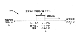
いずれの場合においても、システムの実施形態に、102秒からピコ秒(10-12秒)の範囲で動作する高速シャッターの超短パルスレーザを含む可能性がある。このようなシステムは、複数の短い遮断間隔を導入した後、薄膜物質の表面および埋め込み界面からの試料位置でのSHG信号生成を監視するために使用できる。これらの間隔は、対象の電場減衰を監視するようにタイミングを合わせることができる。 In either case, embodiments of the system may include a fast shutter ultrashort pulse laser operating in the range of 10 2 seconds to picoseconds (10 −12 seconds). Such a system can be used to monitor SHG signal generation at the sample location from the surface and buried interfaces of thin film materials after introducing multiple short interruption intervals. These intervals can be timed to monitor electric field decay of interest.
本システムはまた、光回線遅延を含む可能性がある。遅延線は、特に分散補償および偏光制御光学系と組み合わせた場合、ファイバに基づく装置である可能性がある。あるいは、遅延線はミラーに基づき、マクドナルドの米国特許第6147799号、ビショップ等の第6356377号、またはウー等の第6751374号明細書の実施例に相似する可能性がある。いずれの場合にも、遅延は、物質のレーザ調査をピコ秒(10-12秒)~フェムト秒(10-15秒)、おそらくはアト秒(10-18秒)の範囲で行うためのシステムで使用される。このような調査は、単一の減衰曲線に沿った複数の電荷減衰依存のデータ点を検出するのに役立つ場合がある。 The system may also include optical line delays. The delay line can be a fiber-based device, especially when combined with dispersion compensation and polarization control optics. Alternatively, the delay line may be mirror-based and similar to the embodiments of McDonald's US Pat. No. 6,147,799, Bishop et al., No. 6,356,377, or Wu et al., No. 6,751,374. In either case, the delay is used in systems for laser interrogation of materials in the range of picoseconds ( 10-12 seconds) to femtoseconds ( 10-15 seconds), and possibly attoseconds ( 10-18 seconds). be done. Such an investigation may be useful for detecting multiple charge decay dependent data points along a single decay curve.
本対象の方法は、連続する充電イベントの後に取得した減衰データ点についてSHG信号を測定することを含む方法を含む。SHG信号を取得するための条件は、各充電イベントで異なる可能性がある。さらに、連続する充電イベント間の時間間隔は異なる場合がある。この方法では、複数のデータ点(少なくとも二つ、通常は三つ以上)を相関させて、単一の複合減衰曲線として表すことができる。別の方法では、破壊が最小限の(すなわち、SHG信号を生成するために使用される放射が物質を有意には充電しない)SHG信号調査イベントが単一の充電イベント後に使用される。 The subject method includes measuring a SHG signal for decay data points acquired after successive charging events. The conditions for obtaining the SHG signal may be different for each charging event. Furthermore, the time intervals between successive charging events may vary. In this method, multiple data points (at least two, usually three or more) can be correlated and represented as a single composite attenuation curve. In another method, a minimally destructive SHG signal probing event (ie, the radiation used to generate the SHG signal does not significantly charge the material) is used after a single charging event.
さらに別の過渡的な電荷減衰を決定するための方法は、試料物質(より正確に、光放射により充電されたその構造)からの放電電流を測定することを含む。この信号の時間依存性(動力学)は、SHG計測を採用した場合と同じように扱うことができる。さらに、上記のように、そのような計測は、一つの減衰間隔、および/または充電に続く所与のレベルへの複数のそれらにわたる期間で行われ得る。いずれにせよ、そのような使用のための特定電極のハードウェアについて以下に詳述する。 Yet another method for determining transient charge decay involves measuring the discharge current from the sample material (more precisely, its structure charged by optical radiation). The time dependence (dynamics) of this signal can be handled in the same way as when SHG measurement is employed. Further, as described above, such measurements may be made over one decay interval and/or over multiple periods of time to a given level following charging. In any event, specific electrode hardware for such use is detailed below.
充電または充電レベルに関しては、電荷動態を標準の線形時間または対数時間スケールに対して観測したとき、見かけの飽和点でもよい。上記について、対象の方法論は、必要に応じて、重要な情報をもたらす可能性がある充電速度を観測、記録、および分析する。 With respect to charge or charge level, there may be an apparent saturation point when charge dynamics are observed relative to a standard linear or logarithmic time scale. Regarding the above, the subject methodology optionally observes, records, and analyzes charging rates, which can yield important information.
連続する充電/調査イベントについて、試料の初期充電状態を測定し飽和レベルが初期充電状態から遠くない場合、システムは、さらなるまたは後続の特性評価を省略してよい。この状況において「遠くない」と見なすことが可能な場合として、対象のツールを使用していつ一定時間サンプリングするかを学習することによって決定される、初期充電状態に対する電荷増加が約1%~約10%である場合を意味する可能性がある。 For successive charging/survey events, if the initial state of charge of the sample is measured and the saturation level is not far from the initial state of charge, the system may omit further or subsequent characterization. In this situation, what can be considered "not far" is a charge increase relative to the initial state of charge of about 1% to about This may mean a case of 10%.
換言すれば、いわゆる「飽和」とは、相対的な用語である。線形時間スケールを使用すると、物質は非常にすばやく飽和状態になる。しかし、充電に関連するSHG信号強度を10~100秒の対数スケールで観測した場合、飽和の後半部分は異なる時定数で生じ、相対的により緩やかまたは時間を要することが観測できる。したがって、本明細書で提供する方法論の実施例は、飽和までの充電について論じているが、遅延および他のタイミングは、見かけの飽和に関して生じると見なすことができる。達するのに不必要に時間を要する100%の飽和のための完全な量の時間を待機するのでなく、装置は、完全に飽和するまでにかかる時間に関係なく、見かけの飽和に到達する、または重要なパラメータを抽出できる時間まで遅延させる可能性がある。 In other words, so-called "saturation" is a relative term. Using a linear time scale, the material becomes saturated very quickly. However, when observing the SHG signal strength associated with charging on a logarithmic scale of 10 to 100 seconds, it can be observed that the second half of saturation occurs with a different time constant and is relatively slower or takes longer. Therefore, although the methodological examples provided herein discuss charging to saturation, delays and other timing can be considered to occur with respect to apparent saturation. Rather than waiting the full amount of time for 100% saturation, which takes an unnecessarily long time to reach, the device reaches apparent saturation regardless of the time it takes to reach full saturation, or This may delay the time until important parameters can be extracted.
また、飽和に向かう(例えば、SHG監視に関連して)充電の量または程度を監視する場合に、本対象の方法およびシステムは、意味のある減衰曲線情報を生成しながら、飽和未満(上記で説明したように)の充電および/または再充電レベルで動作できることを理解するべきである。しかし、そのような測定でなく、近似飽和が既知のパラメータのとき(例えば、所定の物質を対象ツールで経験することにより)、飽和充電を目標レベルとして使用する。 Additionally, when monitoring the amount or extent of charging toward saturation (e.g., in connection with SHG monitoring), the subject methods and systems can produce meaningful decay curve information while still producing meaningful decay curve information. It should be understood that it is possible to operate at charging and/or recharging levels (as described). However, rather than such measurements, the saturation charge is used as the target level when the approximate saturation is a known parameter (e.g., by experience with the target tool with a given material).
また、テストする試料の両端のDCバイアスを導入することにより、物質の分析を補助できる。DCバイアスを使用すると、光誘導電圧が影響を与える前に、界面での初期電荷分布が積極的に変化する。そうするためには、テストする試料を、試料上面プローブを使用して試料の両端にDCバイアスを印加するための接地として使用し得る導電性チャックの上に据え付ける可能性がある。さらに、表面プローブを使用することなく、同様の誘導電圧バイアスを導入する他の手段について、2014年4月17日出願の米国仮出願第61/980860号明細書「ウエハ計測技術」の第IV節「電場バイアスSHG技術」に詳述されている。 Additionally, the analysis of materials can be aided by introducing a DC bias across the sample being tested. Using a DC bias actively changes the initial charge distribution at the interface before the photoinduced voltage takes effect. To do so, the sample to be tested may be mounted on a conductive chuck that can be used as a ground to apply a DC bias across the sample using a top-of-sample probe. Additionally, other means of introducing similar induced voltage biases without the use of surface probes are discussed in Section IV of U.S. Provisional Application No. 61/980,860, "Wafer Metrology Techniques," filed April 17, 2014. It is detailed in "Electric field bias SHG technology".
また、対象のシステムは、電荷減衰決定用遮断型分析に含まれる一次レーザに加えて二次光源を使用する可能性がある。そのような光源の一式を、2014年4月17日出願の米国仮出願第61/980860号明細書「ウエハ計測技術」の第I節「ポンプおよびプローブ型SHG計測」に詳述されるように、放射ポンプ/プローブの組み合わせとして使用する可能性がある。 Also, the subject system may use a secondary light source in addition to the primary laser included in the blocked analysis for charge decay determination. A set of such light sources may be used as detailed in Section I, "Pump and Probe SHG Metrology," of U.S. Provisional Application No. 61/980,860, "Wafer Metrology Technology," filed April 17, 2014. , has the potential to be used as a radiation pump/probe combination.
すべての本発明の実施形態は、本明細書に記載した手法に関連する方法のそれぞれを単独で、または参照する同時係属中の特許出願からの要素部品もしくは特徴、その方法を実行するためのハードウェア、そのハードウェアおよび製品(プロダクト・バイ・プロセスを含む)を組み込んだ生産システムと組み合わせて含む。 All embodiments of the present invention may include component parts or features from co-pending patent applications that refer to each of the methods described herein alone or to hardware for carrying out the methods. ware, its hardware and products (including product-by-process) in combination with embedded production systems.
(第III部)
様々なバイアス場(例えば、磁場バイアス、DCバイアス、ならびに/または容量結合および/もしくは変化する磁場を伴う、AC場だけで誘導した電圧バイアス)のSHGに基づくシステムおよびそれらの使用方法について説明する。これらについて順番に扱う。それらは、独立して、および/または組み合わせたシステムで使用することができる。本明細書に記載した様々な実施形態は、上記の手法に関連した方法のそれぞれ、上記方法を実行するハードウェア、そのハードウェアおよび製品(プロダクト・バイ・プロセスを含む)を組み込む生産システムを含む。
(Part III)
SHG-based systems of various bias fields (e.g., magnetic field bias, DC bias, and/or AC field-only induced voltage bias with capacitive coupling and/or changing magnetic field) and their use are described. We will address these in turn. They can be used independently and/or in combined systems. Various embodiments described herein include each of the methods associated with the techniques described above, hardware for performing the methods, and production systems that incorporate the hardware and products (including product-by-process). .
(磁場バイアス)
静的または変化する磁場を試料に印加すると、物質の二次の光学感受率テンソルの変化を引き起こすであろう。したがって、磁場を使用して、試料からのSHG信号を最適値まで増加させることができる。さらに、以下でさらに説明するように、変化する磁場を使用してバイアスを誘導することができる。
(Magnetic field bias)
Applying a static or changing magnetic field to the sample will cause a change in the second-order optical susceptibility tensor of the material. Therefore, a magnetic field can be used to increase the SHG signal from the sample to an optimal value. Additionally, a varying magnetic field can be used to induce bias, as discussed further below.
(DC接触プローブを除くための誘導電圧バイアス)
積層半導体物質のSHG応答を特性評価するためのシステムおよび方法が記載について記載する。当該物質は、システム内の接触バイアスプローブを使用せずに、その界面全体にわたる別個の電場を受け、当該電場は、プローブレーザのパルスおよび/または検出器の開閉を、試料に印加する所定振幅の可変もしくはパルス状ACバイアスに同期させ、調査すべき表面に対応のまたは配位された誘導電圧場を生成できる。
(Induced voltage bias to exclude DC contact probe)
Systems and methods for characterizing the SHG response of layered semiconductor materials are described. The material is subjected to a separate electric field across its interface without the use of a contact-biased probe in the system, which electric field is composed of probe laser pulses and/or detector openings and closings of a predetermined amplitude applied to the sample. Synchronized to a variable or pulsed AC bias, an induced voltage field can be generated corresponding to or coordinated with the surface to be investigated.
対象ハードウェアは、SHG装置(例えば、2014年4月17日出願の米国仮出願第61/980860号明細書「ウエハ計測技術」の第II節「電荷減衰測定のシステムおよび方法」に詳述するもの)を、試料の「装置」面に、またはそれに沿って非接触で電圧を誘導する手段(例えば、誘導するように構成された部品)とともに含む。そのような手段または部品は、プローブを備えた裏面接触か、または導電チャックを介してのいずれかであり、裏面接触プローブまたはそのようなチャックと通信もする電力源に接続した容量結合プローブを伴う。あるいは、その多層界面に外部電圧場を誘導する目的のため、試料に変化する磁場を印加することによってである。 The target hardware may include SHG equipment (e.g., as detailed in Section II "Systems and Methods for Charge Decay Measurement" of U.S. Provisional Application No. 61/980,860, "Wafer Metrology Techniques," filed April 17, 2014). (e.g., a component configured to induce) a non-contact voltage inducing voltage at or along the "apparatus" surface of the sample. Such means or components may be either back-contact with a probe or via a conductive chuck, with a back-contact probe or a capacitively coupled probe connected to a power source that also communicates with such a chuck. . Alternatively, by applying a varying magnetic field to the sample for the purpose of inducing an external voltage field at the multilayer interface.
可変波形(必要に応じてAC)電源が生成する過渡電場によって(上記の手法のいずれかを介して)、多層半導体物質の界面全体の電場を誘導する。電圧および物質界面電場の関係は、伝達関数またはその他の方法でモデル化できる。これには、さまざまな(容量性またはその他の)外的影響を考慮することも含まれる。この関数の出力について、特定の振幅および周波数のAC(または他の)電流を与えることにより、界面の電場振幅値がほぼ瞬時的に一定となるテスト点のSHG特性評価のため、レーザシャッタおよび/または光子カウンタを同時にトリガするタイミング合図として使用する可能性がある。このように、システムにより、接触電気プローブを介して上面(すなわち、基板の装置層)に印加する一定の(DC)電圧を模擬することができる。 A variable waveform (optionally AC) power supply generates a transient electric field (via any of the techniques described above) to induce an electric field across the interface of the multilayer semiconductor material. The relationship between voltage and material interface electric field can be modeled as a transfer function or in other ways. This also includes considering various external influences (capacitive or otherwise). For the output of this function, the laser shutter and/or Or it could be used as a timing cue to trigger photon counters simultaneously. In this manner, the system can simulate a constant (DC) voltage applied to the top surface (ie, the device layer of the substrate) via the contact electrical probe.
試料の裏面にACを直接適用すると、システムは、「中性」または接地状態のチャック、ならびに平衡電位のバルクおよび装置層から始まる。次に、バルクまたは多層半導体物質の基板層とガルバニック接触するチャックに交流バイアスを印加する。装置層は、埋め込みの酸化物層によってバルクから分離され、導体に直接接続しないため、装置およびバルク層間に電位場または電圧が生成(すなわち、誘導)される。 Applying AC directly to the back side of the sample, the system starts with a "neutral" or grounded chuck and bulk and device layers at equilibrium potential. An alternating current bias is then applied to the chuck in galvanic contact with the substrate layer of the bulk or multilayer semiconductor material. Because the device layer is separated from the bulk by a buried oxide layer and does not connect directly to a conductor, a potential field or voltage is created (i.e., induced) between the device and bulk layer.
あるいは、試料の上面に接触することなくその近傍(約1~約2mm以内)に存在する容量結合プローブを使用する可能性がある。この点において好ましい手法では、ウエハ全体を覆う(しかし、接触しない)大きさのプレートであって、当該プレートは、入射レーザが試料に向かって通過し、かつ試料から出力するSHGビームが通過するための小さい穴を備え、空中停止している可能性がある。 Alternatively, one might use a capacitively coupled probe that is in close proximity (within about 1 to about 2 mm) to the top surface of the sample without touching it. A preferred approach in this regard is a plate sized to cover (but not touch) the entire wafer, through which the incident laser passes towards the sample, and through which the SHG beam exiting from the sample passes. It has a small hole and may be suspended in the air.
いくつかの実装では、非接触電極を、MEMS技術を用いて実現することができる。例えば、一実装では、Siウエハの両面を酸化することができる。次に、スパイラルまたはグリッド状の電極を、ウエハの一つまたは複数の場所に堆積させることによって配置することができる。酸化物物質は、これらの場所でウエハの裏側から取り除くことができる。電極に印加された電磁場は、そのような実装において、近接場誘導結合を介してウエハを誘導的にバイアスすることができる。外部電流によって生成された磁場を使用して、堆積された電極に電流を誘導することにより、ウエハ全体に電流を生成することができる。非接触プローブを実装する他の方法も使用できる。 In some implementations, non-contact electrodes can be realized using MEMS technology. For example, in one implementation, both sides of the Si wafer can be oxidized. A spiral or grid-like electrode can then be placed by depositing it on one or more locations on the wafer. Oxide material can be removed from the backside of the wafer at these locations. The electromagnetic field applied to the electrodes can inductively bias the wafer through near-field inductive coupling in such implementations. A magnetic field generated by an external current can be used to generate current across the wafer by inducing current in the deposited electrodes. Other methods of implementing non-contact probes can also be used.
いずれの場合においても、SHG法を、試料を調査するために使用し、例えば、2014年4月17日出願の米国仮出願第61/980860号明細書「ウエハ計測技術」の第I節「ポンプおよびプローブ型SHG計測」の部分に詳述がある。同一のことは、以下に論じる他の実施形態に関しても当てはまる。 In either case, the SHG method is used to interrogate the sample, for example in Section I of U.S. Provisional Application Ser. and probe-type SHG measurement" section for detailed information. The same applies with respect to other embodiments discussed below.
とにかく、対象の実施形態では、界面の両端間の電圧の関数としてSHGを監視することが望ましいので、SHG信号を電力源と同期させるであろう。この同期は、SHG信号生成およびSHG信号処理ソフトウェアに使用するレーザ、レーザ単独、またはSHG信号処理ソフトウェアのみを、電圧変化とともに時間的に制御することによって達成できる。チャックの電圧も制御できる。 Regardless, in the subject embodiment it is desirable to monitor the SHG as a function of the voltage across the interface, so the SHG signal would be synchronized with the power source. This synchronization can be achieved by temporally controlling the laser used for SHG signal generation and SHG signal processing software, the laser alone, or only the SHG signal processing software with voltage changes. The chuck voltage can also be controlled.
この同期の利点は、DCバイアスのSHG測定値と同様の電圧バイアスのSHG測定値を、ウエハの表面に接触電圧バイアスプローブを使用することなく取得できることである。DCバイアスを印加する代わりに、システムはSHG測定および/または生成と同期したACバイアスを使用して、電圧サイクルの別々の点でSHGデータを収集する。ACバイアスは、近接場誘導結合を使用して、または試料の容量性結合を介して印加できる。これらのバイアス技術で収集したSHGデータは、DCバイアスのSHGと同一の物質特性情報を生成する。 The advantage of this synchronization is that voltage-biased SHG measurements similar to DC-biased SHG measurements can be obtained without using a contact voltage bias probe at the surface of the wafer. Instead of applying a DC bias, the system collects SHG data at separate points in the voltage cycle using an AC bias that is synchronized with SHG measurements and/or generation. AC bias can be applied using near-field inductive coupling or via capacitive coupling of the sample. SHG data collected with these bias techniques produces the same material property information as DC biased SHG.
ノイズを低減または最小化し、界面の両端の電圧の関数として統計学的に適切な指標を得るために、以下に詳述するように、複数の光子計数ウィンドウが望ましい可能性がある。 To reduce or minimize noise and obtain statistically relevant metrics as a function of voltage across the interface, multiple photon counting windows may be desirable, as detailed below.
(界面リークを特性評価するための誘導電圧バイアス)
積層(例えば、半導体)物質の層間の界面リーク電流および/またはキャリア注入エネルギーについて、SHGおよび上記のような積層半導体物質に印加する電圧変化(例えば、交流の、可変および/もしくはパルス状電圧または電流信号、あるいは試料の装置層内に電圧変化を誘導するように磁場を変化させる装置)を利用して特性評価するシステムおよび方法を説明する。
(Induced voltage bias to characterize interfacial leakage)
For interfacial leakage currents and/or carrier injection energies between layers of stacked (e.g., semiconductor) materials, voltage changes (e.g., alternating current, variable and/or pulsed voltages or currents) applied to the SHG and stacked semiconductor materials as described above. A system and method for characterization using a signal or a device that varies a magnetic field to induce a voltage change in a device layer of a sample is described.
交流の、可変および/もしくはパルス状電圧を積層の半導体/誘電体構造物質に印加しながら、あるいは印加直後に、当該積層半導体物質に向けられたパルスレーザによって生成される光パルスからのSHG応答を測定することによって、層間の界面リーク電流および/またはキャリア注入エネルギーを特性評価することができる。いくつかの実施形態では、誘導電圧の減衰時定数の関数として界面からのSHG信号の時間発展を測定することができる。これにより、界面全体の電荷キャリアの移動度に関する情報が得られる。 While or immediately after applying an alternating current, variable and/or pulsed voltage to the stacked semiconductor/dielectric structure material, the SHG response from an optical pulse generated by a pulsed laser directed at the stacked semiconductor material is generated. By measuring, the interlayer interfacial leakage current and/or carrier injection energy can be characterized. In some embodiments, the time evolution of the SHG signal from the interface can be measured as a function of the decay time constant of the induced voltage. This provides information about the mobility of charge carriers across the interface.
(キャリア注入エネルギーしきい値を特性評価するための誘導電圧バイアス)
積層半導体物質における、誘電体への光誘導電荷キャリア注入のエネルギーしきい値を決定するため、波長可変レーザ励起の使用に代わる、試料の装置層での変動電場と関係するSHG測定について、そのシステムおよび方法を説明する。より具体的には、誘電体への光誘導電荷キャリア注入に必要なエネルギーしきい値を測定するために、前述の物質を実質的に単色の入射光子ビームに曝露してSHGを生成させ、次に曝露された積層半導体物質の界面両端の電圧を増分的に変化させ、SHG応答が大幅な屈曲もしくは不連続性を示すか、または以前の測定値からの勾配が突然変化するまで、各増分電圧変化でSHG信号数を測定することができる。この勾配の変化は、最大もしくは最小(例えば、極大もしくは極小)、または尖点、あるいは階段関数などの可能性がある。これらすべてのプロセスによる正味の電荷変化の伝達は、第三高調波注入電流、強電場による誘電体への「順方向」リーク電流、および「逆方向」放電リーク電流の寄与の積分として説明できる。方程式の形式では、以下となる。

A system for SHG measurements associated with varying electric fields in device layers of a sample as an alternative to the use of tunable laser excitation to determine the energy threshold for photoinduced charge carrier injection into dielectrics in layered semiconductor materials. and explain the method. More specifically, to measure the energy threshold required for photoinduced charge carrier injection into a dielectric, the aforementioned material is exposed to a substantially monochromatic incident beam of photons to produce SHG, and then Incrementally change the voltage across the interface of a stacked semiconductor material exposed to The number of SHG signals can be measured by the change. This change in slope can be a maximum or minimum (eg, a local maximum or minimum), or a cusp, or a step function, or the like. The net charge change transfer due to all these processes can be described as the integral of the contributions of the third harmonic injection current, the "forward" leakage current into the dielectric due to the strong electric field, and the "reverse" discharge leakage current. In equation form, it is:
すべての本発明の実施形態は、本明細書に記載した手法に関連する方法のそれぞれを単独で、または参照する同時係属中の特許出願からの要素部品もしくは特徴、その方法を実行するためのハードウェア、そのハードウェアおよび製品(プロダクト・バイ・プロセスを含む)を組み込んだ生産システムと組み合わせて含む。 All embodiments of the present invention may include component parts or features from co-pending patent applications that refer to each of the methods described herein alone or to hardware for carrying out the methods. ware, its hardware and products (including product-by-process) in combination with embedded production systems.
本明細書に開示したシステム、方法および装置は、それぞれがいくつかの革新的な態様を有し、それら単一のものは、いずれも、本明細書に開示した望ましい属性に対して単独で原因を有するわけではない。様々なシステムおよび方法の実施例について以下に説明する。 The systems, methods, and apparatus disclosed herein each have several innovative aspects, each single one of which is solely responsible for the desirable attributes disclosed herein. It does not necessarily mean that it has. Examples of various systems and methods are described below.
(パターン化されたウエハの評価)
(実施例1)
試料表面を光学的に調査するためのシステムであって、
可変エネルギーの放射を放出するように構成された光源と、
複数の領域を有するパターン化された構造を含む調査表面からの放射による第二高調波発生(SHG)光を検出するように構成された光学的検出器と、
さまざまな領域向けに、一組の調査条件を決定し、前述の組の調査条件に基づく第1のSHG光信号を受信し、前述の領域で検出した前述のSHG光の特性を決定し、前述の組の調査条件を更新し、前述の更新された組の調査条件に基づく第2のSHG光信号を受信するように構成された制御電子機器と、
を含む。
(実施例2)
実施例1のシステムであって、前述の組の調査条件は、入射光に関連する偏光状態を含む励起偏光状態を含む。
(実施例3)
実施例1または2のシステムであって、前述の組の調査条件は、出力信号に関連する偏光状態を含む出力偏光状態を含む。
(実施例4)
実施例1、2、または3のシステムであって、前述の組の調査条件は、入射面およびパターンの向き間の方位角を含む。
(実施例5)
上記実施例のいずれかのシステムであって、前述の組の調査条件は、
入射光に関連する偏光状態を含む励起偏光状態と、
出力信号に関連する偏光状態を含む出力偏光状態と、
入射面およびパターンの向き間の方位角と、
を含む。
(実施例6)
実施例4または5のシステムであって、前述の調査表面は、前述の方位角を選択するための回転ステージによって配置される。
(実施例7)
実施例4、5、または6のシステムであって、前述の制御電子機器は、前述の組の調査条件を決定するために、前述のパターンの構造に基づいて前述の方位角を選択するように構成される。
(実施例8)
実施例4~7のいずれかのシステムであって、前述の制御電子機器は、前述の組の調査条件を決定するために、前述の出力信号が大きくなるように前述の方位角を選択するように構成される。
(実施例9)
実施例4~8のいずれかのシステムであって、前述の制御電子機器は、前述の組の調査条件を更新するために、前述のパターンの構造による影の低減に関連する前述の方位角を選択するように構成される。
(実施例10)
実施例9のシステムであって、前述の構造は溝を含み、
前述の制御電子機器は、前述の組の調査条件を更新するために、前述の入射面が前述の溝の長さと同一直線上になるように前述の方位角を選択するように構成される。
(実施例11)
実施例2または4のシステムであって、前述の制御電子機器は、前述の組の調査条件を更新するために、前述の出力信号が大きくなるように、前述の励起偏光状態を更新するように構成される。
(実施例12)
実施例3または4のシステムであって、前述の制御電子機器は、前述の組の調査条件を更新するために、前述の出力信号が大きくなるように、前述の出力偏光状態を更新するように構成される。
(実施例13)
上記実施例のいずれかのシステムであって、前述の領域で検出された前述のSHG光の特性を決定することは、前述の第2のSHG光信号が前述の第1のSHG光信号よりも大きいかどうかを決定することを含む。
(実施例14)
上記実施例のいずれかのシステムであって、前述の領域で検出された前述のSHG光の特性を決定することは、前述の第2のSHG光信号の信号対ノイズ比が前述の第1のSHG光信号の信号対ノイズ比よりも大きいかどうかを決定することを含む。
(実施例15)
上記実施例のいずれかのシステムであって、前述の第2のSHG光信号の強度は、前述の第1のSHG光信号よりも大きい。
(実施例16)
試料の表面を光学的に調査する方法であって、
光源を使用して、調査表面に放射を供給し、
光学的検出器を使用して、放射によって生成された第二高調波発生(SHG)効果信号を検出し、
一組の調査条件を決定し、
前述の組の調査条件に基づく第1のSHG光信号を受信し、
前述表面の領域で検出した前述のSHG光の特性を決定し、
前述の組の調査条件を更新し、
前述の更新された組の調査条件に基づく第2のSHG光信号を受信する、
ことを含む。
(実施例17)
実施例16の方法であって、前述の組の調査条件は、入射光に関連する偏光状態を含む励起偏光状態を含む。
(実施例18)
実施例16または17の方法であって、前述の組の調査条件は、出力信号に関連する偏光状態を含む出力偏光状態を含む。
(実施例19)
実施例16、17、または18の方法であって、前述の組の調査条件は、入射面およびパターンの向き間の方位角を含む。
(実施例20)
実施例16の方法であって、前述の組の調査条件は、
入射光に関連する偏光状態を含む励起偏光状態と、
出力信号に関連する偏光状態を含む出力偏光状態と、
入射面およびパターンの向き間の方位角と、
を含む。
(実施例21)
実施例19または20の方法であって、前述の調査表面は、前述の方位角を選択するための回転ステージによって配置される。
(実施例22)
実施例19~21のいずれかの方法であって、前述の組の調査条件を決定することは、前述調査表面のパターン構造に基づいて前述の方位角を選択することを含む。
(実施例23)
実施例19~22のいずれかの方法であって、前述の組の調査条件を更新することは、前述調査表面のパターン構造による影の低減に関連する前述の方位角を選択することを含む。
(実施例24)
実施例23の方法であって、前述のパターン構造は溝を含み、
前述の組の調査条件を更新することは、前述の入射面が前述の溝の長さと同一直線上になるように前述の方位角を選択することを含む。
(実施例25)
実施例17または20の方法であって、前述の組の調査条件を更新することは、前述の出力信号が大きくなるように、前述の励起偏光状態を選択することを含む。
(実施例26)
実施例18または20の方法であって、前述の組の調査条件を更新することは、前述の出力信号が大きくなるように、前述の出力偏光状態を選択することを含む。
(実施例27)
実施例16~26のいずれかの方法であって、前述の第2のSHG光信号の強度は、前述の第1のSHG光信号よりも大きい。
(実施例28)
実施例16~27のいずれかの方法であって、前述表面の領域で検出された前述のSHG光の特性を決定することは、前述の第2のSHG光信号が前述の第1のSHG光信号よりも大きいかどうかを決定することを含む。
(実施例29)
実施例16~28のいずれかの方法であって、前述表面の領域で検出された前述のSHG光の特性を決定することは、前述の第2のSHG光信号の信号対ノイズ比が前述の第1のSHG光信号の信号対ノイズ比よりも大きいかどうかを決定することを含む。
(実施例30)
実施例1~15のいずれかのシステムであって、前述のシステムは、前述の試料が製造ラインまたは生産ラインにある間、前述の試料をインラインで調査するように構成される。
(実施例31)
実施例1~15、または30のいずれかのシステムは、さらに、前述の試料にポンプ放射を提供するためのポンプ源を含む。
(実施例32)
実施例16~29のいずれかのシステムは、前述の調査表面に放射を適用することが、ポンプ放射およびプローブ放射を適用することを含む。
(実施例33)
実施例16~29、または32のいずれかのシステムは、前述の試料の調査を、前述の試料が製造または生産ラインにある間インラインで実行する。
(Evaluation of patterned wafer)
(Example 1)
A system for optically investigating a sample surface, the system comprising:
a light source configured to emit radiation of variable energy;
an optical detector configured to detect second harmonic generation (SHG) light due to radiation from an interrogation surface that includes a patterned structure having a plurality of regions;
determining a set of probing conditions for different areas, receiving a first SHG light signal based on said set of probing conditions, determining characteristics of said SHG light detected in said area; control electronics configured to update a set of probing conditions and receive a second SHG optical signal based on said updated set of probing conditions;
including.
(Example 2)
In the system of Example 1, the aforementioned set of interrogation conditions includes an excitation polarization state that includes a polarization state associated with the incident light.
(Example 3)
The system of Example 1 or 2, wherein the aforementioned set of interrogation conditions includes an output polarization state that includes a polarization state associated with an output signal.
(Example 4)
In the system of Examples 1, 2, or 3, the aforementioned set of interrogation conditions includes the azimuthal angle between the plane of incidence and the orientation of the pattern.
(Example 5)
In the system of any of the above embodiments, the above set of investigation conditions are:
an excitation polarization state including a polarization state associated with the incident light;
an output polarization state including a polarization state associated with the output signal;
the azimuthal angle between the plane of incidence and the orientation of the pattern;
including.
(Example 6)
The system of Example 4 or 5, wherein said interrogation surface is positioned by a rotation stage for selecting said azimuthal angle.
(Example 7)
The system of
(Example 8)
The system of any of Examples 4 to 7, wherein the control electronics is configured to select the azimuth angle such that the output signal is large in order to determine the set of investigation conditions. It is composed of
(Example 9)
The system of any of Examples 4-8, wherein said control electronics determines said azimuth angle associated with shadow reduction due to said pattern structure to update said set of survey conditions. Configured to select.
(Example 10)
The system of Example 9, wherein the structure includes a groove;
Said control electronics are configured to select said azimuth angle such that said entrance plane is collinear with said groove length in order to update said set of survey conditions.
(Example 11)
The system of
(Example 12)
The system of
(Example 13)
In the system of any of the above embodiments, determining the characteristics of the SHG light detected in the region includes determining that the second SHG optical signal is higher than the first SHG optical signal. Including determining whether it is larger.
(Example 14)
In the system of any of the above embodiments, determining the characteristics of the above-mentioned SHG light detected in the above-mentioned region is such that the signal-to-noise ratio of the above-mentioned second SHG light signal is equal to or less than the above-mentioned first and determining whether the signal-to-noise ratio of the SHG optical signal is greater than the signal-to-noise ratio of the SHG optical signal.
(Example 15)
In the system of any of the above embodiments, the intensity of the second SHG optical signal is greater than the first SHG optical signal.
(Example 16)
A method for optically investigating the surface of a sample, the method comprising:
using a light source to provide radiation to the investigation surface;
detecting a second harmonic generation (SHG) effect signal produced by the radiation using an optical detector;
determine a set of research conditions;
receiving a first SHG optical signal based on the aforementioned set of investigation conditions;
determining the characteristics of the aforementioned SHG light detected in the aforementioned surface region;
Update the aforementioned set of survey conditions,
receiving a second SHG optical signal based on the updated set of survey conditions;
Including.
(Example 17)
The method of Example 16, wherein the aforementioned set of interrogation conditions includes an excitation polarization state that includes a polarization state associated with the incident light.
(Example 18)
The method of Example 16 or 17, wherein the set of interrogation conditions includes an output polarization state that includes a polarization state associated with an output signal.
(Example 19)
The method of Examples 16, 17, or 18, wherein the aforementioned set of interrogation conditions includes an azimuthal angle between the plane of incidence and the orientation of the pattern.
(Example 20)
The method of Example 16, in which the aforementioned set of investigation conditions are:
an excitation polarization state including a polarization state associated with the incident light;
an output polarization state including a polarization state associated with the output signal;
the azimuthal angle between the plane of incidence and the orientation of the pattern;
including.
(Example 21)
The method of Example 19 or 20, wherein said interrogation surface is positioned by a rotation stage for selecting said azimuthal angle.
(Example 22)
The method of any of Examples 19-21, wherein determining the set of interrogation conditions includes selecting the azimuthal angle based on a pattern structure of the interrogation surface.
(Example 23)
The method of any of Examples 19-22, wherein updating said set of survey conditions includes selecting said azimuth angle associated with reduction of shadows due to patterned structure of said survey surface.
(Example 24)
The method of Example 23, wherein the pattern structure includes a groove;
Updating said set of survey conditions includes selecting said azimuth such that said entrance plane is collinear with said groove length.
(Example 25)
The method of Example 17 or 20, wherein updating the set of interrogation conditions includes selecting the excitation polarization state such that the output signal is large.
(Example 26)
The method of Example 18 or 20, wherein updating the set of interrogation conditions includes selecting the output polarization state such that the output signal is large.
(Example 27)
In the method of any one of Examples 16 to 26, the intensity of the second SHG optical signal is greater than the first SHG optical signal.
(Example 28)
In the method of any of Examples 16 to 27, determining the characteristics of the SHG light detected in the region of the surface includes determining the characteristics of the SHG light detected in the region of the surface, such that the second SHG light signal is detected by the first SHG light signal. including determining whether the signal is greater than the signal.
(Example 29)
The method of any of Examples 16 to 28, wherein determining the characteristics of said SHG light detected in said region of said surface comprises determining said second SHG light signal having a signal-to-noise ratio as described above. and determining whether the signal-to-noise ratio of the first SHG optical signal is greater than the signal-to-noise ratio of the first SHG optical signal.
(Example 30)
The system of any of Examples 1-15, wherein said system is configured to interrogate said sample in-line while said sample is on a manufacturing line or production line.
(Example 31)
The system of any of Examples 1-15, or 30 further includes a pump source for providing pump radiation to the sample.
(Example 32)
The system of any of Examples 16-29, wherein applying radiation to the interrogation surface includes applying pump radiation and probe radiation.
(Example 33)
The system of any of Examples 16-29 or 32 performs the aforementioned sample investigation in-line while the aforementioned sample is on the manufacturing or production line.
(パラメトリックモデリング)
(実施例1)
第二高調波発生を使用して試料を特性評価するためのシステムであって、
前述試料からの第二高調波発生光を生成する調査光ビームを前述試料に伝播させるように構成された光源と、
前述試料から前述第二高調波発生光を受信するように構成された検出器と、
一回目の前述第二高調波発生光の第1の強度レベルおよび前述一回目よりも後の二回目の前述第二高調波発生光の第2の強度レベル間の差に基づいて前述試料の特性を取得するように構成された電子機器と、
を含む。
(実施例2)
実施例1のシステムであって、前述電子機器は、前述一回目の前述第二高調波発生光の前述第1の強度レベルおよび前述一回目より後の前述二回目の前述第2の強度レベル間の差の、前述一回目の前述第二高調波発生光の前述第1の強度レベルに対する比に基づいて前述試料の特性を取得するように構成される。
(実施例3)
実施例1または2のシステムは、さらに、前述一回目および前述二回目間の時間に、前述第二高調波発生光の強度レベルを少なくとも一つ追加して取得することを含む。
(実施例4)
実施例1~3のいずれかのシステムであって、前述試料について取得した前述特性は、前述試料の酸化物層の厚さ、酸化物層内のバルクトラップの量、表面特性の少なくとも一つを含む。
(実施例5)
実施例1~4のいずれかのシステムであって、前述試料について取得した前述特性は、前記試料の酸化物層の厚さを含む。
(実施例6)
実施例1~5のいずれかのシステムであって、前述試料について取得した前述特性は、酸化物層内のバルクトラップの量を含む。
(実施例7)
実施例1~6のいずれかのシステムであって、前述試料について取得した前述特性は、前述試料の表面特性を含む。
(実施例8)
第二高調波発生を使用して界面領域を有する試料を特性評価する方法であって、
計測システムの光源からの放射を前述界面領域に向け、
前述計測システムの光学的検出システムを用いて、前述界面領域からの第二高調波発生光を検出し、
前述第二高調波発生光の強度レベルに基づいて前述試料の特性を決定する。
(実施例9)
実施例8の方法であって、前述界面領域は、半導体層および酸化物層間の接合、金属および酸化物間の接合、第1の半導体領域および第2の半導体領域間の接合を含む。
(実施例10)
実施例8または9の方法であって、前述第二高調波発生光の前述強度レベルに基づき前述試料について決定した前述特性は、前述試料の酸化物層の充電量、前述試料の界面領域の充電量、または前述試料の界面結合状態に関連する情報の少なくとも一つを含む。
(実施例11)
実施例8~10のいずれかの方法であって、前述第二高調波発生光の前述強度レベルに基づき前述試料について決定した前述特性は、前述試料の酸化物層の充電量を含む。
(実施例12)
実施例8~11のいずれかの方法であって、前述第二高調波発生光の前述強度レベルに基づき前述試料について決定した前述特性は、前述試料の界面領域の充電量を含む。
(実施例13)
実施例8~12のいずれかの方法であって、前述第二高調波発生光の前述強度レベルに基づき前述試料について決定した前述特性は、前述試料の界面結合状態に関連する情報を含む。
(実施例14)
第二高調波発生を使用して界面領域を有する試料を特性評価する方法であって、
計測システムの光源からの放射を前述界面領域に向け、
前述計測システムの光学的検出システムを用いて、前述界面領域からの第二高調波発生光を検出し、
一回目の前述第二高調波発生光の第1の強度レベルおよび前述一回目より後の二回目の前述第二高調波発生光の第2の強度レベル間の差に基づいて、前述試料の特性を決定する。
(実施例15)
実施例14の方法であって、前述電子機器は、前述一回目の前述第二高調波発生光の前述第1の強度レベルおよび前述一回目より後の前述二回目の前述第2の強度レベル間の差の、前述一回目の前述第二高調波発生光の前述第1の強度レベルに対する比に基づいて前述試料の特性を取得するように構成される。
(実施例16)
実施例14または15の方法は、さらに、前述一回目および前述二回目間の時間に、前述第二高調波発生光の強度レベルを少なくとも一つ追加して取得することを含む。
(実施例17)
実施例14~16のいずれかの方法は、前述試料について取得した前述特性は、前述試料の酸化物層の厚さ、酸化物層内のバルクトラップの量、表面特性の少なくとも一つを含む。
(実施例18)
実施例14~17のいずれかの方法であって、前述試料について取得した前述特性は、前記試料の酸化物層の厚さを含む。
(実施例19)
実施例14~18のいずれかの方法であって、前述試料について取得した前述特性は、酸化物層内のバルクトラップの量を含む。
(実施例20)
実施例14~19のいずれかの方法であって、前述試料について取得した前述特性は、前述試料の表面特性を含む。
(実施例21)
実施例1~8のいずれかのシステムであって、前述のシステムは、前述の試料が製造ラインまたは生産ラインにある間、前述の試料をインラインで調査するように構成される。
(実施例22)
実施例1~8、または21のいずれかのシステムは、さらに、前述の試料にポンプ放射を提供するためのポンプ源を含む。
(実施例23)
実施例8~13のいずれかの方法は、前述の界面領域に放射を向けることが、ポンプ放射およびプローブ放射を適用することを含む。
(実施例24)
実施例8~13、または23のいずれかの方法は、前述の試料の特性評価を、前述の試料が製造または生産ラインにある間インラインで実行する。
(実施例25)
実施例14~20のいずれかの方法は、前述の界面領域に放射を向けることが、ポンプ放射およびプローブ放射を適用することを含む。
(実施例26)
実施例14~20、または25のいずれかの方法は、前述の試料の特性評価を、前述の試料が製造または生産ラインにある間インラインで実行する。
(parametric modeling)
(Example 1)
A system for characterizing a sample using second harmonic generation, the system comprising:
a light source configured to propagate an interrogation light beam to the sample that generates second harmonic generated light from the sample;
a detector configured to receive the second harmonic generated light from the sample;
The characteristics of the sample based on the difference between the first intensity level of the second harmonic generation light at the first time and the second intensity level of the second harmonic generation light at the second time after the first time. an electronic device configured to obtain
including.
(Example 2)
(Example 3)
The system of the first or second embodiment further includes acquiring at least one additional intensity level of the second harmonic generation light during the time between the first and second times.
(Example 4)
In the system of any of Examples 1 to 3, the characteristics obtained for the sample include at least one of the thickness of the oxide layer, the amount of bulk traps in the oxide layer, and the surface characteristics of the sample. include.
(Example 5)
In the system of any of Examples 1-4, the characteristics obtained for the sample include the thickness of the oxide layer of the sample.
(Example 6)
In the system of any of Examples 1-5, the characteristics obtained for the sample include the amount of bulk traps within the oxide layer.
(Example 7)
In the system of any of Examples 1 to 6, the properties acquired for the sample include surface properties of the sample.
(Example 8)
A method for characterizing a sample having an interfacial region using second harmonic generation, the method comprising:
directing radiation from the light source of the measurement system toward the aforementioned interface region;
detecting second harmonic generated light from the interface region using an optical detection system of the measurement system;
The characteristics of the sample are determined based on the intensity level of the second harmonic generated light.
(Example 9)
The method of Example 8, wherein the interface region includes a junction between a semiconductor layer and an oxide layer, a junction between a metal and an oxide, and a junction between a first semiconductor region and a second semiconductor region.
(Example 10)
In the method of Example 8 or 9, the characteristics determined for the sample based on the intensity level of the second harmonic generated light include the amount of charge in the oxide layer of the sample, the charge in the interface region of the sample. and at least one of information related to the interfacial bonding state of the sample.
(Example 11)
In the method of any of Examples 8 to 10, the characteristic determined for the sample based on the intensity level of the second harmonic generated light includes the amount of charge of the oxide layer of the sample.
(Example 12)
In the method of any of Examples 8 to 11, the characteristic determined for the sample based on the intensity level of the second harmonic generated light includes the amount of charge in the interface region of the sample.
(Example 13)
In the method of any of Examples 8-12, the characteristic determined for the sample based on the intensity level of the second harmonic generated light includes information related to the interfacial bonding state of the sample.
(Example 14)
A method for characterizing a sample having an interfacial region using second harmonic generation, the method comprising:
directing radiation from the light source of the measurement system toward the aforementioned interface region;
detecting second harmonic generated light from the interface region using an optical detection system of the measurement system;
The characteristics of the sample are determined based on the difference between the first intensity level of the second harmonic generation light at the first time and the second intensity level of the second harmonic generation light at the second time after the first time. Determine.
(Example 15)
(Example 16)
The method of Example 14 or 15 further includes acquiring at least one additional intensity level of the second harmonic generation light during the time between the first time and the second time.
(Example 17)
In the method of any of Examples 14 to 16, the properties obtained for the sample include at least one of the thickness of the oxide layer of the sample, the amount of bulk traps in the oxide layer, and the surface properties.
(Example 18)
The method of any of Examples 14-17, wherein the property obtained for the sample includes the thickness of an oxide layer of the sample.
(Example 19)
The method of any of Examples 14-18, wherein the characteristics obtained for the sample include the amount of bulk traps within the oxide layer.
(Example 20)
The method of any of Examples 14-19, wherein the properties obtained for the sample include surface properties of the sample.
(Example 21)
The system of any of Examples 1-8, wherein said system is configured to interrogate said sample in-line while said sample is on a manufacturing line or production line.
(Example 22)
The system of any of Examples 1-8, or 21 further includes a pump source for providing pump radiation to the sample.
(Example 23)
The method of any of Examples 8-13, wherein directing radiation to the aforementioned interfacial region includes applying pump radiation and probe radiation.
(Example 24)
The method of any of Examples 8-13 or 23 performs the characterization of the sample in-line while the sample is on the manufacturing or production line.
(Example 25)
The method of any of Examples 14-20, wherein directing radiation to the aforementioned interfacial region includes applying pump radiation and probe radiation.
(Example 26)
The method of any of Examples 14-20 or 25 performs the characterization of the sample in-line while the sample is on the manufacturing or production line.
(テスト構造)
(実施例1)
半導体装置製造構造であって、
半導体基板と、
半導体と接触して界面領域を形成する酸化物層、および周囲環境に曝露された導電領域、ならびに前記周囲環境に曝露された前記導電領域および前記酸化物層間の電気経路を提供する相互接続を含む、前記半導体基板上に支持されたテスト構造と、を含み、
前記テスト構造は、前記界面領域において光学計測システムから光ビームを受信し、前記光学計測システムによって受信することができる第二高調波発生光を生成するように構成される。
(実施例2)
実施例1の半導体装置製造構造であって、前記界面領域は、前記酸化物層および前記半導体基板によって形成される。
(実施例3)
実施例1の半導体装置製造構造であって、前記界面領域は、前記酸化物層および前記半導体基板上の半導体の層によって形成される。
(実施例4)
実施例1~3のいずれかの半導体装置製造構造であって、前記半導体基板上に支持された集積回路装置をさらに含む。
(実施例5)
実施例1~4のいずれかの半導体装置製造構造であって、前記テスト構造は、二つの集積回路間の空間に含まれる。
(実施例6)
実施例1~5のいずれかの半導体装置製造構造であって、前記テスト構造は、前記半導体装置製造構造が個別のダイを形成するために切断される空間に含まれる。
(実施例7)
実施例1~6のいずれかの半導体装置製造構造であって、前記テスト構造は、機能するトランジスタとして構成されていない。
(実施例8)
実施例1~7のいずれかの半導体装置製造構造であって、前記テスト構造は、集積回路に電気的に接続されていない。
(実施例9)
実施例1~8のいずれかの半導体装置製造構造であって、前記相互接続は、酸化物層の側に配置され、それによって前記界面領域への光学的アクセスを提供する。
(実施例10)
実施例1~9のいずれかの半導体装置製造構造であって、前記テスト構造は、前記酸化物層上に障壁層をさらに含む。
(実施例11)
実施例10に記載の半導体装置製造構造であって、前記障壁層は、TiNを含む。
(実施例12)
実施例10または11に記載の半導体装置製造構造であって、前記障壁層は、約1nm~約5nmの厚さを有する。
(実施例13)
実施例1~12のいずれかの半導体装置製造構造であって、前記半導体装置製造構造は、半導体と接触して第2の界面領域を形成する第2の酸化物層を含む、第2のテスト構造をさらに含み、
前記第2のテスト構造は、前記第2の界面領域において光学計測システムから光ビームを受信し、前記光学計測システムによって受信することができる第二高調波発生光を生成するように構成される。
(実施例14)
実施例13の半導体装置製造構造であって、前記第2のテスト構造は、前記周囲環境に曝露された電気接点パッドに電気的に接続されていない。
(実施例15)
実施例13または14の半導体装置製造構造であって、前記第2のテスト構造は、二つの集積回路間の空間に含まれる。
(実施例16)
実施例13~15のいずれかの半導体装置製造構造であって、前記テスト構造は、前記半導体装置製造構造が個別のダイを形成するために切断される空間に含まれる。
(実施例17)
実施例13~16のいずれかの半導体装置製造構造前記第2のテスト構造は、機能するトランジスタとして構成されていない。
(実施例18)
実施例13~17のいずれかの半導体装置製造構造であって、前記第2のテスト構造は、集積回路に電気的に接続されていない。
(実施例19)
実施例13~18のいずれかの半導体装置製造構造であって、前記第2のテスト構造は、前記酸化物層上に障壁層をさらに含む。
(実施例20)
実施例19の半導体装置製造構造であって、前記障壁層は、TiNを含む。
(実施例21)
実施例19または20の半導体装置製造構造であって、前記障壁層は、約1nm~約5nmの厚さを有する。
(実施例22)
第二高調波発生を使用して試料を特性評価するためのシステムであって、
前記試料に光ビームを向けるように構成された光源と、
前記ビームが前記試料に入射する位置を変更するための位置決めシステムと、
前記試料からの第二高調波発生光を受信するように構成された光学的検出システムと、
前記試料に前記光ビームが入射する場所を前記位置決めシステムを使用して制御し、かつ前記第二高調波発生光に基づく前記光学的検出システムからの信号を受信するように構成された電子機器と、を含み、
前記電子機器は、前記光ビームを、半導体と接触して界面領域を形成する酸化物層、および周囲環境に曝露された導電領域、ならびに前記周囲環境に曝露された前記導電領域および前記酸化物層間の電気経路を提供する相互接続を含むテスト構造に向け、前記光ビームは、前記界面領域に入射し、生成される第二高調波発生光を前記光学的検出システムで受信するように構成される。
(実施例23)
実施例22のシステムであって、前記電子機器は、さらに、前記テスト構造からの前記第二高調波発生信号に基づいて、前記界面領域のプロセス誘導充電の効果を特性評価するように構成される。
(実施例24)
実施例22に記載のシステムであって、前記電子機器は、さらに、前記テスト構造からの前記第二高調波発生信号に基づいて、プロセス誘導充電の効果に起因する前記界面領域の電気的特性の変化を決定するように構成される。
(実施例25)
実施例22~24のいずれかのシステムであって、前記電子機器は、前記光ビームを、半導体と接触して第2の界面領域を形成する第2の酸化物層を含む、第2のテスト構造に向け、前記光ビームは、前記第2の界面領域に入射し、生成される第二高調波発生光を前記光学的検出システムで受信するように構成される。
(実施例26)
実施例25のシステムであって、前記第2のテスト構造は、前記周囲環境に曝露された導電領域に電気的に接続されていない。
(実施例27)
実施例25または26のシステムであって、前記電子機器は、さらに、前記テスト構造からの前記第二高調波発生光および前記第2のテスト構造からの前記第二高調波発生光の比較に基づいて、前記界面領域のプロセス誘導充電の効果を特性評価するように構成される。
(実施例28)
実施例25または26のシステムであって、前記電子機器は、さらに、前記テスト構造からの前記第二高調波発生光および前記第2のテスト構造からの前記第二高調波発生光の比較に基づいて、プロセス誘導充電の効果に起因する前記界面領域の電気的特性の変化を決定するように構成される。
(実施例29)
実施例25または26のシステムであって、前記電子機器は、さらに、前記テスト構造からの前記第二高調波発生光および前記第2のテスト構造からの前記第二高調波発生光の差に基づいて、前記界面領域のプロセス誘導充電の効果を特性評価するように構成される。
(実施例30)
プロセス誘導充電の効果に起因する半導体装置の界面領域に関連する電気的特性の変化を決定する方法であって、
界面領域、前記界面領域上の誘電体物質、および周囲環境に曝露された前記誘電体物質上面の導電領域、ならびに前記界面領域および前記導電領域間の前記誘電体物質を介する電気的接続を提供する相互接続、を含むテスト構造を提供し、
前記界面境域上に計測システムの少なくとも一つの光源から放射を向け、
前記計測システムの光学的検出システムによって、前記界面領域からの第二高調波発生光を検出する。
(実施例31)
実施例30の方法であって、前記界面領域は、半導体層および酸化物層間の接合を含む。
(実施例32)
実施例30または31の方法であって、前記界面領域に関連する電気的特性の変化を決定することをさらに含む。
(実施例33)
実施例30~32のいずれかの方法であって、
第2の界面領域を含む第2のテスト構造を提供し、
前記第2の界面境域上に少なくとも一つの光源から放射を向け、
前記計測システムの光学的検出システムにより、前記第2の界面領域からの第二高調波発生光を検出する、ことをさらに含む。
(実施例34)
実施例33の方法であって、前記第2の界面領域は、電気的に導電領域に接続されていない。
(実施例35)
実施例33または34の方法であって、前記界面領域からの前記第二高調波発生光および前記第2の界面領域からの前記第二高調波発生光に基づいて、前記テスト構造の前記界面領域に関連する電気的特性の変化を決定する、ことをさらに含む。
(実施例36)
実施例22~29のいずれかのシステムであって、前記システムは、前記試料が製造または生産ラインにある間インラインで前記試料を特性評価するように構成される。
(実施例37)
実施例22~29または36のいずれかのシステムであって、前記試料にポンプ放射を提供するためのポンプ源をさらに備える。
(実施例38)
実施例30~35のいずれかの方法であって、前記界面領域に放射を向けることは、ポンプ放射およびプローブ放射を適用することを含む。
(実施例39)
実施例30~35または38のいずれかの方法であって、前記試料の前記界面領域に関連する電気的特性の変化を決定することは、前記試料が製造または生産ラインにある間インラインで行われる。
(test structure)
(Example 1)
A semiconductor device manufacturing structure,
a semiconductor substrate;
an oxide layer in contact with a semiconductor to form an interfacial region, and a conductive region exposed to an ambient environment, and an interconnect providing an electrical path between the conductive region exposed to the ambient environment and the oxide layer. , a test structure supported on the semiconductor substrate;
The test structure is configured to receive a light beam from an optical metrology system at the interface region and generate second harmonic generated light that can be received by the optical metrology system.
(Example 2)
In the semiconductor device manufacturing structure of Example 1, the interface region is formed by the oxide layer and the semiconductor substrate.
(Example 3)
In the semiconductor device manufacturing structure of Example 1, the interface region is formed by the oxide layer and a semiconductor layer on the semiconductor substrate.
(Example 4)
The semiconductor device manufacturing structure according to any one of Examples 1 to 3 further includes an integrated circuit device supported on the semiconductor substrate.
(Example 5)
In the semiconductor device manufacturing structure according to any one of Examples 1 to 4, the test structure is included in a space between two integrated circuits.
(Example 6)
The semiconductor device manufacturing structure of any of Examples 1-5, wherein the test structure is included in a space where the semiconductor device manufacturing structure is cut to form individual dies.
(Example 7)
In the semiconductor device manufacturing structure according to any one of Examples 1 to 6, the test structure is not configured as a functioning transistor.
(Example 8)
In the semiconductor device manufacturing structure according to any one of Examples 1 to 7, the test structure is not electrically connected to the integrated circuit.
(Example 9)
The semiconductor device fabrication structure of any of Examples 1-8, wherein the interconnect is located on a side of an oxide layer, thereby providing optical access to the interfacial region.
(Example 10)
In the semiconductor device manufacturing structure according to any one of Examples 1 to 9, the test structure further includes a barrier layer on the oxide layer.
(Example 11)
In the semiconductor device manufacturing structure according to Example 10, the barrier layer includes TiN.
(Example 12)
The semiconductor device manufacturing structure according to Example 10 or 11, wherein the barrier layer has a thickness of about 1 nm to about 5 nm.
(Example 13)
The semiconductor device manufacturing structure according to any one of Examples 1 to 12, wherein the semiconductor device manufacturing structure includes a second oxide layer in contact with the semiconductor to form a second interface region. further including the structure,
The second test structure is configured to receive a light beam from an optical metrology system at the second interface region and generate second harmonic generated light that can be received by the optical metrology system.
(Example 14)
In the semiconductor device manufacturing structure of Example 13, the second test structure is not electrically connected to the electrical contact pad exposed to the surrounding environment.
(Example 15)
In the semiconductor device manufacturing structure of Example 13 or 14, the second test structure is included in a space between two integrated circuits.
(Example 16)
The semiconductor device manufacturing structure of any of Examples 13-15, wherein the test structure is included in a space in which the semiconductor device manufacturing structure is cut to form individual dies.
(Example 17)
Semiconductor device manufacturing structure according to any one of Examples 13 to 16 The second test structure is not configured as a functioning transistor.
(Example 18)
In the semiconductor device manufacturing structure according to any one of Examples 13 to 17, the second test structure is not electrically connected to the integrated circuit.
(Example 19)
In the semiconductor device manufacturing structure according to any one of Examples 13 to 18, the second test structure further includes a barrier layer on the oxide layer.
(Example 20)
Embodiment 19 In the semiconductor device manufacturing structure of Example 19, the barrier layer includes TiN.
(Example 21)
In the semiconductor device manufacturing structure of Example 19 or 20, the barrier layer has a thickness of about 1 nm to about 5 nm.
(Example 22)
A system for characterizing a sample using second harmonic generation, the system comprising:
a light source configured to direct a light beam onto the sample;
a positioning system for changing the position at which the beam is incident on the sample;
an optical detection system configured to receive second harmonic generated light from the sample;
electronics configured to control where the light beam is incident on the sample using the positioning system and to receive a signal from the optical detection system based on the second harmonic generated light; , including;
The electronic device directs the light beam between an oxide layer in contact with a semiconductor to form an interface region and a conductive region exposed to the surrounding environment, and between the conductive region exposed to the surrounding environment and the oxide layer. the light beam is incident on the interface region and configured to receive generated second harmonic generated light at the optical detection system. .
(Example 23)
Example 22. The system of Example 22, wherein the electronic device is further configured to characterize an effect of process-induced charging of the interface region based on the second harmonic generated signal from the test structure. .
(Example 24)
Example 22. The system of Example 22, wherein the electronic device further determines, based on the second harmonic generation signal from the test structure, an electrical characteristic of the interfacial region due to an effect of process-induced charging. configured to determine a change.
(Example 25)
The system of any of Examples 22-24, wherein the electronic device directs the light beam to a second test comprising a second oxide layer in contact with a semiconductor to form a second interface region. The light beam is directed toward the structure and configured to be incident on the second interface region and to receive the generated second harmonic generated light at the optical detection system.
(Example 26)
Example 25. The system of Example 25, wherein the second test structure is not electrically connected to the conductive area exposed to the surrounding environment.
(Example 27)
The system of Example 25 or 26, wherein the electronic device further comprises a method based on a comparison of the second harmonic generated light from the test structure and the second harmonic generated light from the second test structure. and is configured to characterize the effect of process-induced charging of the interfacial region.
(Example 28)
The system of Example 25 or 26, wherein the electronic device further comprises a method based on a comparison of the second harmonic generated light from the test structure and the second harmonic generated light from the second test structure. and configured to determine changes in electrical properties of the interfacial region due to effects of process-induced charging.
(Example 29)
The system of Example 25 or 26, wherein the electronic device further comprises a method based on a difference between the second harmonic generated light from the test structure and the second harmonic generated light from the second test structure. and is configured to characterize the effect of process-induced charging of the interfacial region.
(Example 30)
A method for determining changes in electrical properties associated with an interface region of a semiconductor device due to effects of process-induced charging, the method comprising:
providing an interfacial region, a dielectric material on the interfacial region, and a conductive region on top of the dielectric material exposed to an ambient environment, and an electrical connection between the interfacial region and the conductive region through the dielectric material; provide test structures including interconnects,
directing radiation from at least one light source of a metrology system onto the interfacial boundary;
An optical detection system of the metrology system detects second harmonic generated light from the interface region.
(Example 31)
The method of Example 30, wherein the interface region includes a junction between a semiconductor layer and an oxide layer.
(Example 32)
The method of Example 30 or 31, further comprising determining a change in electrical properties associated with the interfacial region.
(Example 33)
The method according to any one of Examples 30 to 32,
providing a second test structure including a second interfacial region;
directing radiation from at least one light source onto the second interfacial boundary;
The method further includes detecting second harmonic generated light from the second interface region by an optical detection system of the measurement system.
(Example 34)
The method of Example 33, wherein the second interface region is not electrically connected to a conductive region.
(Example 35)
The method of Example 33 or 34, wherein the interfacial area of the test structure is determined based on the second harmonic generated light from the interfacial area and the second harmonic generated light from the second interfacial area. further comprising determining a change in electrical properties associated with the electrical property.
(Example 36)
The system of any of Examples 22-29, wherein the system is configured to characterize the sample in-line while the sample is on a manufacturing or production line.
(Example 37)
The system of any of Examples 22-29 or 36, further comprising a pump source for providing pump radiation to the sample.
(Example 38)
The method of any of Examples 30-35, wherein directing radiation to the interfacial region includes applying pump radiation and probe radiation.
(Example 39)
The method of any of Examples 30-35 or 38, wherein determining the change in electrical properties associated with the interfacial region of the sample is performed in-line while the sample is on a manufacturing or production line. .
図によって、異なる本発明の変形例について種々の実施形態の態様を図式的に説明する。
(第I部)
図1は、対象の方法に関連して使用できるようなシステム100の図である。他の適切なシステムの変形例について、2014年4月17日出願の米国仮出願第61/980860号明細書「ウエハ計測技術」の第II節「電荷減衰測定のシステムおよび方法」に、例えば、中間の光学、光学遅延線を含めることおよび任意の電極機能などに関して提示がある。
(Part I)
FIG. 1 is a diagram of a
図示のように、システム100には、真空チャック30により保持された試料ウエハ20に電磁放射の調査ビーム12を向ける一次またはプローブレーザ10が含まれる。図1Bに示すように、チャック30は、xおよびyステージ、ならびに必要に応じて、レーザが向けられる場所に対してウエハ全体の試料位置22を位置決めするための回転ステージをも含むか、またはそれらのステージ上に設定される。xyステージにより、他のハードウェアを動かすことなく、複数のウエハ表面位置または場所22をスキャンすることが可能になる。回転ステージにより、必要に応じて、特性評価する物質のひずみ、関連する欠陥または懸念領域など、結晶構造のSHGに対する影響を評価することが可能になる。さらなる任意の特徴、態様および/またはチャック30の用途について、2014年4月17日出願の米国仮出願第61/980860号明細書「ウエハ計測技術」の第IV節「電場バイアスSHG技術」に提示がある。試料位置22は、一つまたは複数の層を含むことができる。試料位置22は、少なくとも二つの層を含む複合基板を含むことができる。試料位置22は、二つの異なる物質間(例えば、二つの異なる半導体物質間、不純物が異なる二つの半導体物質間、半導体および酸化物間、半導体および誘電体物質間、半導体および金属、または酸化物および金属間)の界面を含むことができる。
As shown,
システム100を使用したとき、検出器40に向け反射された放射ビーム14は、SHG信号を含むであろう。検出器は、光電子増倍管、CCDカメラ、アバランシェ検出器、フォトダイオード検出器、ストリークカメラ、およびシリコン検出器のいずれであってもよい。システム100はまた、一つまたは複数のシャッター型装置50を含み得る。使用するシャッターハードウェアの種類は、レーザ放射を遮断する、投棄する、または他の方法で試料位置から離れる方向に向ける時間枠に依存する。ポッケルスセルまたはカーセルなどの電子光学遮断装置を使用して、非常に短い遮断期間(つまり、作動時間が10-9~10-12秒程度の)を得ることができる。
When using
より長い遮断時間間隔(例えば、約10-5秒以上)のためには、機械的シャッターまたはフライホイールのチョッパー型装置を用いる可能性がある。しかし、電子光学遮断装置を使用すると、以下の方法に従って、より広範囲の物質をテストできる。非常に短い時間間隔、通常、ピコ秒からマイクロ秒程度で離散的に開閉することができる光子計数システム44を使用して、時間依存信号の計数を解決することができる。より高速な時間枠の場合、上記のように光学遅延線を組み込むことができる。
For longer interruption time intervals (eg, about 10 −5 seconds or more), mechanical shutters or flywheel chopper-type devices may be used. However, using electro-optical blocking devices, a wider range of materials can be tested according to the following method. Counting of time-dependent signals can be resolved using a
システム100は、ポンプ光源とも呼ばれる追加の電磁放射源60を含むことができる。様々な実施形態において、放射源60は、指向性ビーム62を放出するものとして示されるレーザ、または発散もしくは光学的にコリメートされたパルス64を放出するUVフラッシュランプであり得る。レーザ源の場合、そのビーム62は、ビーム12と同一直線上であり得る(例えば、追加のミラーまたはプリズムなどによって向きを変える)。光源60の出力波長は、約80nmから約1000nmのどこであってもよい。この範囲のより短い波長(例えば、約450nm未満)を使用すると、より長い波長よりも少ない光子を使用して、かつ/またはより低いピーク強度で電荷励起を駆動することが可能である。
フラッシュランプの場合、1フラッシュ当りのエネルギー、またはフラッシュ時の電力レベルは、基板物質に依存する可能性がある。1フラッシュ当りの総エネルギー1J~10kJを生成するフラッシュランプが、完全空乏型シリコン・オン・インシュレータ(FD-SOI)に適切であろう。ただし、パルスまたは定常的なUV光源も使用可能であろう。ポンプの特性および用途における重要な要素は、電荷キャリアを調査対象の物質の誘電体中に注入することである。適切なフラッシュランプのメーカーには、米国Hellma社、および浜松フォトニクス株式会社が含まれる。 For flash lamps, the energy per flash, or power level during a flash, can depend on the substrate material. Flash lamps producing 1 J to 10 kJ of total energy per flash may be suitable for fully depleted silicon-on-insulator (FD-SOI). However, pulsed or constant UV light sources could also be used. An important factor in the properties and applications of the pump is the injection of charge carriers into the dielectric of the substance under investigation. Manufacturers of suitable flash lamps include Hellma Corporation, USA, and Hamamatsu Photonics Corporation.
レーザを光源60として使用する場合、ナノ秒、ピコ秒、またはフェムト秒、あるいはより高速のパルスレーザ源のいずれであってもよい。連続固体レーザの可能性さえある。様々な実施形態では、ポンプ源は波長を調整可能である。調整可能なレーザに関して市販されている選択肢には、スペクトラ・フィジックス社のVelocity、およびVortex Tunable Laserがある。さらに、調整可能な固体ソリューションを、LOTIS社のLT-22xxシリーズの固体レーザから入手できる。
If a laser is used as the
レーザまたはフラッシュランプのいずれとして提供するにしても、ポンプ源60は、比較的高い平均電力を有するように選択し得る。これは、約10mW~約10Wが可能であるが、より通常は、約100mW~約4Wと調査物質に依存し(繰り返しになるが、考慮すべきことは、電荷キャリアを物質の界面(例えば、誘電体界面)中に注入するような、電荷キャリア移動度の誘導を保証することである)、物質固有の値であり得る。ポンプ源60の平均電力は、物質の光学的損傷のしきい値以下であるように選択される。例えば、ポンプ源60は、調査物質がシリコンを含む場合、シリコンの光学的損傷しきい値を超えないように、平均光電力が1~2Wを有するように選択することができる。
Whether provided as a laser or a flashlamp, pump
プローブレーザ10は、ナノ秒、ピコ秒、またはフェムト秒、あるいはより高速のパルスレーザ源のいずれであってもよい。必要なピーク電力、波長、信頼性を有する、現在市販のレーザの二つの選択肢は、ドープファイバーおよびチタンサファイア装置である。コヒレント社のVITESSEおよびスペクトラ・フィジックス社のMAI TAIレーザが好適なチタンサファイアの例である。フェムトレーザーズ社およびその他のメーカーも、他の適切なチタンサファイア装置を製造する。適切なドープファイバーレーザを、IMRA、OneFive、およびToptica Photonicsが製造する。基板物質およびポンプ種によっては、浜松など多くのメーカーのピコ秒、および/または、ナノ秒レーザも、選択肢になる可能性がある。レーザ10は、約100nm~約2000nmの波長範囲において約10kW~1GWのピーク電力で動作するが、電力供給は平均で150mW未満となる可能性がある。
Probe
その他種々の任意の、いわゆる「中間」光学部品を、システム100で使用することができる。例えば、システムは、レーザ10および/または光源60から直接に反射された放射と同軸のSHG信号を選択的に通過させる二色性反射もしくは屈折フィルタ70を含む可能性がある。あるいは、プリズムを使用して、より弱いSHG信号を、何桁も強い反射一次ビームから区別することができる。しかし、プリズムを使用する手法は誤整列に非常に敏感であることが判明しているため、上記の二色性システムが好ましい場合がある。他の選択肢には、回折格子またはペリクルビームスプリッタの使用が含まれる。集束および平行/円柱構造光学系のための光束80を設けてもよい。あるいは、フィルタホイール90、偏光子92、および/またはズームレンズ94の装置もしくはアセンブリを、システムで使用することができる。また、角度(または円弧型)回転調整(検出器に対応する調整を伴うもの)およびインライン光学用部品が望ましい場合もある。
Any of a variety of other so-called "intermediate" optical components may be used in
図1Cに示す実装では、レーザ10からのビーム12を、ビームスプリッタ74によって二つの光路に分割することができる。ビームスプリッタ74は、二つの光路間に不均等にビーム12を分割し得る。例えば、ビーム12のエネルギーの70%を、第1の光路に沿って(例えば、ビーム16として)向けることができ、ビーム12のエネルギーの30%を、第2の光路に沿って(例えば、ビーム18として)向けることができる。別の例として、ビーム12のエネルギーの60%を第1の光路に沿って向けることができ、ビーム12のエネルギーの40%を第2の光路に沿って向けることができる。さらに別の例として、ビーム12のエネルギーの80%を第1の光路に沿って向けることができ、ビーム12のエネルギーの20%を第2の光路に沿って向けることができる。このように、分割を不均等(例えば、70~30%、80~20%、60~40%もしくはその間の任意の範囲、例えば、60~90%を一の経路にかつ40~10%を別の経路に、また、これらの範囲外でも同様)とし、ポンプビームに電力の大半を、プローブビームにその残りを送信し得る。例えば、分割は、ポンプおよびプローブのそれぞれに対して、60~70%対40~30%、70~80%対30~20%、80~90%対20~10%、または90~99.999%対10~0.001%であり得る。異なる実施形態では、例えば、プローブビームは0.001%~49.99%とし、一方、ポンプビームは50.001%~99.999%とし得る。二つのビームの合計は、100%またはそれに近い値にし得る。分割は、特性評価する特定の物質システムによって決まる場合もある。図1Cに示す例では、ビーム12のビームエネルギーの5%は、第1の光路に沿って向けられ、ビーム12のビームエネルギーの95%は、第2の光路に沿って向けられる。
In the implementation shown in FIG. 1C,
ビームスプリッタ74は、誘電体ミラー、スプリッタキューブ、金属被覆ミラー、ペリクルミラーまたは導波路スプリッタを含むことができる。ビーム12が光パルスを含む場合の実装では、ビームスプリッタ74は、光パルスを広げないように二つの光路間にビーム12を分割する、無視できる程度の分散の光学部品を含むことができる。図1Cに示されるように、各ビームは、様々なミラー要素72を使用して方向転換または照準を合わせることができる。
検出器40および/または光子計数システム44からの出力は、電子装置48に入力することができる。電子装置48は、計算装置、コンピュータ、タブレット、マイクロコントローラまたはFPGAとすることができる。電子装置48は、プロセッサ、処理用電子機器、制御用電子機器、処理/制御用電子機器、または一つもしくは複数のソフトウェアモジュールを実行するように構成され得る電子機器を含む。オペレーティングシステムを実行することに加えて、プロセッサは、ウェブブラウザ、電話アプリケーション、電子メールプログラム、または他の任意のソフトウェアアプリケーションを含む一つまたは複数のソフトウェアアプリケーションを実行するように構成され得る。電子装置48は、本明細書で論じる方法を、例えば、RAM、ROM、EEPROM、等のような機械可読非一時的記憶媒体に含まれる命令を実行することにより、実装できる。電子装置48は、ユーザと対話するための表示装置および/またはグラフィックユーザインタフェースを含むことができる。電子装置48は、ネットワークインタフェースを介して一つまたは複数の装置と通信することができる。ネットワークインタフェースは、例えば、有線イーサネット、ブルートゥース(登録商標)、または無線接続などの通信が可能な送信機、受信機、および/もしくはトランシーバを含むことができる。
Output from
他の選択肢に関しては、SHG信号は、それを生成する反射ビームと比較して弱いので、SHG計数の信号対ノイズ比を改善することが望ましい。光子計数システム44の光子計数ゲート時間が、本明細書に記載の遮断および/または遅延プロセスのために減少するにつれて、改善がさらに重要になる。使用する可能性のあるノイズを低減する一つの方法は、光子計数器を積極的に冷却することである。これは、液体窒素やヘリウムなどの極低温流体、またはペルチェ装置を使用した固体冷却を使用して行うことができる。その他の改善分野には、シャッタースピードに関連するマルクスバンク回路(MBC)の使用が含まれる可能性がある。さらに、システム100は、生産ライン環境内のインラインに組み込むことができる。システム100に先行するまたは後続の生産ライン要素には、エピタキシャル成長システム、リソグラフィおよび/または堆積(CVD、PVD、スパッタリング、等)システムのいずれも含まれ得る。
Regarding other options, since the SHG signal is weak compared to the reflected beam that generates it, it is desirable to improve the signal-to-noise ratio of the SHG counts. Improvements become even more significant as the photon counting gate time of
さて、図2A/2Bおよび3A/3Bは、対象のポンプ/プローブシステムをそれらの方法で使用して得られる可能性があるSHG曲線の種類の例を示す概略図である。図2Aおよび2Bでは、そのような信号を得るための時間スケールは、ミリ秒(10-3秒)の程度である。したがって、これらは「高速」プロセスである。以下でさらに説明するように、既存の手法と比較して、時間的に数桁の改善が得られる可能性がある。例えば、SHGプローブ前に、テスト物質全面をUV放射に露光可能なフラッシュランプにより、各点での持続的な測定が必要なくなる可能性があるので、全体的なスキャン時間が劇的に低減する。 2A/2B and 3A/3B are schematic diagrams illustrating examples of the types of SHG curves that may be obtained using the subject pump/probe systems in their manner. In FIGS. 2A and 2B, the time scale for obtaining such a signal is on the order of milliseconds (10 −3 seconds). Therefore, these are "fast" processes. As discussed further below, improvements in time can be of several orders of magnitude compared to existing techniques. For example, a flash lamp capable of exposing the entire surface of the test material to UV radiation prior to the SHG probe may eliminate the need for continuous measurements at each point, thereby dramatically reducing overall scan time.
具体的に、図2AのSHG信号200は、初期強度202で測定されている。この信号は、プローブ源放射を表面位置に適用することにより生成される。ポンプ源放射を(オンしたままのプローブ放射に)与えられた時間差(O1)後に追加すると、信号強度が時間依存曲線204に沿ってより低いレベル206に降下する。逆に、図2BのSHG信号200’は、プローブ放射のみにより生成されたより低いレベル212にあって、時間差(O2)後にポンプ放射を適用すると、時間依存曲線214に沿ってより高い平坦部216まで増加する。信号200および200’は、また、曲線の開始および終了時に時間に依存しない成分または部分を含む。
Specifically, the SHG signal 200 of FIG. 2A is measured at an
図2Aおよび2Bの両観測結果は、対象システムの基板物質および異なるレーザ電力(例えば、この場合、ポンプ電力)に応じて、作製され得る。様々な実施形態において、電荷分離は、光子からの励起後に互いに分離する電子および正孔を含む。レーザの光子によってSiO2伝導帯にシリコン価電子帯から注入された電子は、酸化物の表面上部に主に捕捉される。正孔の大部分は、Si/SiO2界面近傍のシリコン価電子帯の近くに凝集する。入射する放射または内部光電子放出からの励起による電荷キャリアのこの分離は、対象システム内に存在する電場に寄与し、これにより、測定されるSHGが変化する。テスト位置での気体状酸素の存在、問題の試料の組成および構造などのさまざまな要因によって、図2Aまたは2Bのような観測のいずれがなされるかが決まる。 Both observations of FIGS. 2A and 2B can be made depending on the substrate material of the target system and different laser powers (eg, pump power in this case). In various embodiments, charge separation includes electrons and holes separating from each other after excitation from a photon. Electrons injected from the silicon valence band into the SiO 2 conduction band by laser photons are mainly trapped on the upper surface of the oxide. Most of the holes condense near the silicon valence band near the Si/SiO 2 interface. This separation of charge carriers due to excitation from the incoming radiation or internal photoemission contributes to the electric field present within the target system, which changes the measured SHG. Various factors, such as the presence of gaseous oxygen at the test location, the composition and structure of the sample in question, will determine whether observations such as FIG. 2A or 2B are made.
実際に、信号200および200’の組み合わせが観測される例がある。それらの例では、信号強度が最初にピークから降下し、底に達し、再度漸近線まで上昇する。一般に、SHG強度曲線は、非線形感受率テンソルによって決定され、当該テンソルは、分子配向、原子組成、電子構造、および外部場の影響を受ける。界面を横切って移動する電荷キャリアは、SHG信号が発生する界面下位層の構造および電場の電荷状態を変化させる。界面全体の電荷キャリアのタイプ(正または負)、および界面全体の電場の初期状態に応じて、異なる時間依存曲線が観測される。検出されたSHG信号の強度は、スポットサイズ、平均レーザ電力、ピークレーザ電力などのさまざまな要因に依存し、システム100は、約400計数/秒~約7百万計数/秒の範囲の強度を有するSHG信号を検出するように構成することができる。本明細書に記載のポンプ/プローブシステムは、界面を横切って移動する電荷キャリアが飽和レベルに到達するのに必要な時間を短縮することができる。様々な実施形態において、界面を横切って移動する電荷キャリアが飽和レベルに到達するのに必要な時間は、本明細書に記載のポンプ/プローブシステムにおいて1m秒~1000秒とすることができる。界面を含む領域の電荷キャリア密度が飽和を下回ったとき、および界面を含む領域の電荷キャリア密度が飽和レベルに達したときに、SHG信号の時間発展を取得することが有利である可能性があるため、システムは、ポンプ放射をオン/オフした後、約1μ秒以内にSHG信号測定値を取得するように構成することができる。例えば、システムは、ポンプ放射(またはプローブ放射)をオン/オフした後10秒以内に、ポンプ放射をオン/オフした後約6秒以内に、ポンプ放射をオン/オフした後約1秒以内に、ポンプ放射をオフ/オンした後約100m秒以内に、もしくはポンプ放射をオフ/オンした後約1m秒以内に、ポンプ放射をオフ/オンした後約1μ秒以内に、ポンプ放射をオフ/オンした後約1n秒以内に、またはこれらの値のいずれかによって形成される任意の範囲(例えば、1n秒より大きい、1μ秒よりも大きい、1m秒より大きい、期間等)内に、ならびにそれらの範囲外でも同様に、SHG信号測定値を取得するように構成することができる。これらの値および範囲は、単一の点からデータを得るために適用されるが、適切な結像光学系を用いることにより、これをウエハの実質的な領域のウエハ全体まで拡大し、かつ一度に含むようにすることができる。上記の括弧で示すように、これらの値および範囲を、プローブ放射にも適用する。充電時間およびSHG信号の取得に必要な時間を短縮することで、界面のテストを高速化できるため、テストおよび/または製造生産ラインのスループットを向上させることができる。
In fact, there are instances where a combination of
比較のため、図3Aおよび3Bは、既存のSHG技術のように、基板を調査するため放射源(この場合、高い平均電力および高いピーク電力レーザ)を一つのみ使用したときの、対応する物質についてのSHG信号曲線300および300’の概略図である。図3Aおよび3BのSHG信号曲線300および300’を生成するための時間スケールは、数十から数百(102)秒の程度である。 For comparison, Figures 3A and 3B show the corresponding materials when using only one radiation source (in this case a high average power and high peak power laser) to interrogate the substrate, as in existing SHG techniques. 3 is a schematic diagram of SHG signal curves 300 and 300' for FIG. The time scale for generating the SHG signal curves 300 and 300' of FIGS. 3A and 3B is on the order of tens to hundreds (10 2 ) seconds.
そのような時間にわたって、これらの信号(図2Aおよび2Bのような信号)は、初期の302および/または時間依存信号の後に特性評価できる下寄りおよび上寄りの平坦部306、316を含む。このように、類似(または同一)の分析を信号200/200’、および300/300’で実行することが可能であるが、主な違いは、対象のシステム(すなわち、より低いピーク電力フェムト秒プローブレーザを、物質の予備励起用のより高い平均電力ポンプと組み合わせて使用するもの)では、必要な信号情報を取得する際の時間的効率を大幅に向上できることである。さらに、対象の手法により、フィルタホイールまたは他の方法を使用せずに、時間に依存しないSHG測定値をより簡単に決定する方法を提供できる。
Over such time, these signals (such as those in FIGS. 2A and 2B) include lower and
いずれの場合においても、図4は、注入キャリアエネルギーしきい値を決定する方法を示す。この場合、ポンプは、波長可変レーザを含む。これによって、ポンプから試料に入射してから経時的に光子の出力周波数(従って、E=hνによるエネルギー)を高めることができる。観測されるSHG活性を、信号400として示す。ポンプレーザをいわゆる適用または使用し、プローブレーザの適用により生成された初期SHG信号レベル402について、信号が突然の変化(すなわち、404での変曲、不連続、最大、最小、階段関数、尖端、または勾配の急激な変化)をするまで観測する。この時点での周波数が、エネルギーしきい値に対応すると見なされる。様々な実装において、エネルギーしきい値は、一つの半導体物質の価電子帯から他の半導体物質の伝導帯に、例えば、二つの半導体物質、または半導体物質および誘電体物質(例えば、SiおよびSiO2、SiおよびSi3N4、SiおよびTa2O5、SiおよびBaTiO3、SiおよびBaZrO3、SiおよびZrO2、SiおよびHfO2、SiおよびLa2O3、SiおよびAl2O3、SiおよびY2O3、SiおよびZrSiO4)など二つの物質間の界面を横切って電子を輸送するのに必要なエネルギーである。システム100は、約1.0eV~約6.0eVの範囲のエネルギーしきい値を測定するように構成することができる。本明細書に記載のシステムおよび方法は、例えば、二つの異なる半導体間、半導体および金属間、半導体および誘電体間などのような様々な界面のエネルギーしきい値を決定するように構成することができる。
In either case, FIG. 4 shows how to determine the injected carrier energy threshold. In this case, the pump includes a tunable laser. This makes it possible to increase the output frequency of photons (therefore, the energy according to E=hv) over time after they enter the sample from the pump. The observed SHG activity is shown as
図5は、SHGを用いて半導体装置を特性評価する方法の実装について説明するフローチャートである。様々なプロセスフロー経路を示す。そのような方法は全て、502の所望の場所に試料を位置決めすることから開始する可能性がある(例えば、通常は、ウエハ20が固定された後のチャック30を配置することによる)。プログレッシブ位置決め(すなわち、再位置決め)は、さらに説明するように、任意のSHG検出イベント520の後に発生する可能性があり、試料の領域内の複数の表面位置もしくはすべての表面位置、または試料のすべての表面位置をスキャンするためである。あるいは、そのような動作を、検出したSHG信号に関して540で所与の決定をした後に起こし得る(「戻る」選択をいずれも点線で示す)。別の決定に関するさらなる詳細について、上記で参照した本出願の他の部分を参照して理解することができよう。いずれの場合も、試料の位置決めまたは再位置決めに続いて、特定のフロー経路を選択する(または、別のフロー経路を同一の表面位置で連続して実行して、異なるデータを生成することもできる)。
FIG. 5 is a flowchart illustrating implementation of a method for characterizing a semiconductor device using SHG. Illustrating various process flow paths. All such methods may begin by positioning the sample at a desired location at 502 (eg, typically by positioning
一つのプロセスフロー経路(実線部分)に従うと、504でプローブ源放射を、特定場所の試料表面に適用する。次に、506でポンプ源放射を適用する。この実施例では、ポンプ放射について、放射波長を減少させることによって(必要に応じて)光子エネルギーを線形に増加させるさまざまな方法で適用する。得られたSHGを520で検出する。542で信号解析(図4の例に基づく)により、キャリア注入エネルギーしきい値を決定できる。様々な実装では、ポンプ放射のエネルギーは、半導体界面のエネルギーしきい値に対応し得る。したがって、ポンプ放射のエネルギーは、約1.0eV~約6.0eVとし得る。例えば、SiおよびSiO2界面全体のエネルギーしきい値を決定するため、ポンプ放射のエネルギーしきい値を約4.1eV~約5.7eVで変化させ得る。ポンプ放射のエネルギーの変化は、放射の周波数(または波長)を変化させることによって達成することができる。例えば、約3.2eVのエネルギーしきい値の期待値を有する試料を調査するために、ポンプ放射の波長を約443nm~約365nmで変化させることができる。さまざまな実装では、ポンプ放射の光子が2倍のエネルギーを有する電子を生成できるため(例えば、一つの電子が二つの光子を吸収する場合)、ポンプ放射のエネルギーは半導体界面のエネルギーしきい値を下回る可能性がある。このような実装では、充電時間を長くして、解像度および強度を向上させた観測が可能になる。充電時間の増加は、また、試料位置をテストするために必要な時間を増加させ、スループットを減少させ得る。 Following one process flow path (solid line portion), at 504 probe source radiation is applied to the sample surface at a particular location. Next, pump source radiation is applied at 506. In this example, the pump radiation is applied in various ways to linearly increase the photon energy (if necessary) by decreasing the emission wavelength. The obtained SHG is detected at 520. At 542, signal analysis (based on the example of FIG. 4) may determine a carrier injection energy threshold. In various implementations, the energy of the pump radiation may correspond to an energy threshold of the semiconductor interface. Accordingly, the energy of the pump radiation may be between about 1.0 eV and about 6.0 eV. For example, the energy threshold of the pump radiation can be varied from about 4.1 eV to about 5.7 eV to determine the energy threshold across the Si and SiO 2 interface. Varying the energy of the pump radiation can be achieved by changing the frequency (or wavelength) of the radiation. For example, to investigate a sample with an expected energy threshold of about 3.2 eV, the wavelength of the pump radiation can be varied from about 443 nm to about 365 nm. In various implementations, the energy of the pump radiation exceeds the energy threshold of the semiconductor interface because a photon of the pump radiation can generate an electron with twice the energy (e.g., when one electron absorbs two photons). There is a possibility that it will fall below. Such an implementation would allow for longer charging times and observations with increased resolution and intensity. Increasing charging time may also increase the time required to test sample locations and reduce throughput.
別のプロセスフロー経路(破線部分)に従うと、508でポンプ放射を基板に適用する。そのような適用は、直接調査する表面のみ(例えば、レーザによる)か、またはウエハの表面全体(例えば、フラッシュランプを使用する)に向けることができる。次に、510で、調査対象の試料の部分をプローブ源の放射に曝露する。得られたSHGを520で検出する。本方法のポンプ-プローブ-検出の態様について、その後、潜在的に502で試料の再位置決め後、繰り返す可能性がある。しかし、図示のように、動作ボックス508を省略することができ、上記の例のように、基板全体を最初に放射に曝露する場合、再度のポンプを逐次スキャンプロセスから回避させ、または省略してよい。いずれの場合においても、544でSHGに基づく種々の信号解析を行い、本出願の他の箇所で説明するように、ブロック542のエネルギーしきい値の決定以外の決定もできる。
Following an alternative process flow path (dashed portion), pump radiation is applied to the substrate at 508. Such applications can be directed either directly to only the surface to be interrogated (e.g. with a laser) or to the entire surface of the wafer (e.g. using a flashlamp). Next, at 510, a portion of the sample to be investigated is exposed to radiation of a probe source. The obtained SHG is detected at 520. The pump-probe-detection aspect of the method may then be repeated, potentially after repositioning the sample at 502. However, as shown,
別のプロセスフロー経路(一点鎖線部分)に従うと、504および510のプローブ放射を適用直後520のSHG信号データ収集をしながら508のポンプ放射の前後に504および510のプローブ調査を実行する。再び、本方法を再帰的に実行し、基板またはその一領域の全ての部分のような複数の位置をサンプルし、フローチャート要素502に戻り、再位置決め後、プローブ-検出-ポンプ-プローブ-検出の方法もしくはその一部を繰り返すことができる。
Following an alternative process flow path (dotted-dash line section), the probe surveys at 504 and 510 are performed before and after the pump radiation at 508, with SHG signal data collection at 520 immediately after application of the probe radiation at 504 and 510. Again, the method may be performed recursively to sample multiple locations, such as all portions of a substrate or a region thereof, and return to
特に、SHG信号分析の方法または方法の一部(一般的にボックス540および542に包含される)を、瞬時またはほぼ瞬時出力において行うようなリアルタイムに行うことができる。そうすることで、収集データによって決定される任意の分光学的特性を、マシン上か、または遠隔の統合ソフトウェアのいずれかによるソフトウェアパッケージによって計算することができる。あるいは、SHG信号分析を、SHGデータの一部またはすべてを検出または収集後、後処理で処理し得る。
In particular, the SHG signal analysis method or portions of the method (generally encompassed by
本明細書で説明するシステムおよび方法について、試料(例えば、半導体ウエハまたはその一部)を特性評価するために使用できる。例えば、本明細書に記載のシステムおよび方法を使用して、上記のように試料中の欠陥または汚染物質を検出できる。本明細書に記載のシステムおよび方法について、半導体ウエハの製造または生産中に試料を特性評価するように構成できる。したがって、システムおよび方法を、半導体製造施設の半導体製造ラインに沿って使用できる。本明細書に記載のシステムおよび方法を、半導体製造/生産ラインと統合できる。本明細書に記載のシステムおよび方法について、自動化されたウエハ処理機能を備えた半導体製造ラインに統合できる。例えば、システムには、フロントオープニングユニファイドポッド(FOUP)などのウエハカセットを受け入れる機器フロントエンドモジュール(EFEM)を取り付けることができる。これらのカセットのそれぞれを、人間のオペレーターによって、またはカセットを製造/生産ラインに沿ってプロセスからプロセスに移動させる自動カセット処理ロボットによって、それらの機械に配送できる。 The systems and methods described herein can be used to characterize samples (eg, semiconductor wafers or portions thereof). For example, the systems and methods described herein can be used to detect defects or contaminants in a sample as described above. The systems and methods described herein can be configured to characterize samples during semiconductor wafer fabrication or production. Accordingly, the system and method can be used along a semiconductor manufacturing line in a semiconductor manufacturing facility. The systems and methods described herein can be integrated with semiconductor manufacturing/production lines. The systems and methods described herein can be integrated into semiconductor manufacturing lines with automated wafer processing capabilities. For example, the system can be equipped with an equipment front end module (EFEM) that accepts wafer cassettes, such as front opening unified pods (FOUPs). Each of these cassettes can be delivered to the machines by a human operator or by an automated cassette handling robot that moves the cassettes from process to process along the manufacturing/production line.
様々な実施形態では、システムについて、カセットを一度EFEM上に取り付けると、FOUPが開き、そしてロボットアームがFOUPから個々のウエハを選択しシステムに含まれる自動的に作動するドアを通って移動させ、遮光プロセスボックス、およびバイアス可能な真空チャックに入れるように構成できる。チャックは、試料をその上に置くことができるように、ロボットアームと補完し適合するように設計することができる。この過程のある時点で、ウエハをスキャナにかざして、固有のレーザ刻印を特定できる。 In various embodiments, the system includes: once the cassette is mounted on the EFEM, the FOUP is opened, and a robotic arm selects individual wafers from the FOUP and moves them through an automatically actuated door included in the system; It can be configured to be placed in a light-tight process box and a biasable vacuum chuck. The chuck can be designed to complement and fit the robotic arm so that the sample can be placed on it. At some point in the process, the wafer can be held up to a scanner to identify the unique laser markings.
したがって、半導体製造/組み立てラインに統合されるように構成されたシステムは、FOUPまたは他の種類のカセットからの自動ウエハ操作能力、上記のようなEFEMへの統合、ロボット操作と互換性を持つ方法で設計されたチャック、ロボットの棒/アームの動作が可能なように開閉する自動遮光ドア、およびウエハのロード/アンロードおよびウエハ識別のためEFEMに信号を出すソフトウェアを有することができる。 Therefore, a system configured to be integrated into a semiconductor manufacturing/assembly line has the ability to handle automated wafers from FOUPs or other types of cassettes, integration into EFEMs as described above, and methods compatible with robotic operation. It can have a chuck designed with , an automatic light-tight door that opens and closes to allow robot rod/arm movement, and software that signals the EFEM for wafer loading/unloading and wafer identification.
(第II部)
図6Aは、対象の方法に関して使用し得る第1のシステム2100を示す。別のシステム2100’および2100’’を図6Bおよび6Cに示す。各システムには、真空チャック2030により保持された試料ウエハ2020に電磁放射の一次ビーム2012を向ける一次レーザ2010が含まれる。チャック2030は、xおよびyステージ、ならびに必要に応じて、レーザが向けられる場所に対してウエハ全体の試料位置2022を位置決めするための回転ステージをも含むか、またはそれらのステージ上に設定される。検出器2040に向け反射された放射ビーム2014は、SHG信号を含むであろう。検出器は、光電子増倍管、CCDカメラ、アバランシェ検出器、フォトダイオード検出器、ストリークカメラ、およびシリコン検出器のいずれであってもよい。試料位置2022は、一つまたは複数の層を含むことができる。試料位置2022は、少なくとも二つの層を含む複合基板を含むことができる。試料位置2022は、二つの異なる物質間(例えば、二つの異なる半導体物質間、不純物が異なる二つの半導体物質間、半導体および酸化物間、半導体および誘電体物質間、半導体および金属、または酸化物および金属間)の界面を含むことができる。
(Part II)
FIG. 6A shows a
また、各実施形態の共通点は、一つまたは複数のシャッター型装置2050を含むことである。これらを、以下の方法に関連して説明するように使用する。使用するシャッターハードウェアの種類は、レーザ放射を遮断する、投棄する、または他の方法で試料位置から離れる方向に向ける時間枠に依存するであろう。
What each embodiment also has in common is that they include one or more shutter-
ポッケルスセルまたはカーセルなどの電子光学遮断装置を使用して、非常に短い遮断期間(つまり、切り替え時間が10-9~10-12秒程度の)を得ることができる。より長い遮断時間間隔(例えば、約10-5秒以上)のためには、機械的シャッターまたはフライホイールのチョッパー型装置を用いる可能性がある。 Very short interruption periods (ie switching times on the order of 10 −9 to 10 −12 seconds) can be obtained using electro-optical interruption devices such as Pockels cells or Kerrsels. For longer interruption time intervals (eg, about 10 −5 seconds or more), mechanical shutters or flywheel chopper-type devices may be used.
しかし、電子光学遮断装置を使用すると、以下の方法に従って、より広範囲の物質をテストできるであろう。非常に短い時間間隔、通常、ピコ秒からマイクロ秒程度で離散的に開閉することができる光子計数システム2044を使用して、時間依存信号の計数を解決することができる。
However, using an electro-optical blocking device, a wider range of materials could be tested according to the following method. A
ハードウェアについて、前述の方法をより高速な時間枠に押し込むよう企図している。すなわち、図6Cに示すように、システムには、遅延線ハードウェア2060を含めることができる。対応する数の時間遅延調査イベントのための複数の時間設定遅延線間のビーム分割および切り替え(またはシャッターのオン/オフ)が可能である。ただし、可変遅延線は、ポンプのパルス後すぐ(多くの方法では、わずか10-12秒の遅延しか必要ない場合もあるけれども)から数十ナノ秒の時間枠まで、複数の過渡電荷減衰調査イベントに対して単一のソリューションを提供するため、好ましい可能性がある。より遅いキロヘルツの繰り返しレーザを使用する場合、望ましい遅延時間は、マイクロ秒領域に入る可能性さえある。そして、そのようなハードウェアは、対象の方法(方法およびそのようなハードウェアの両方とも、これまで知られていなかったと信じられている)を実行するのに独自に適するが、他の用途にも使用する可能性がある。 For hardware, we intend to push the aforementioned method to a faster time frame. That is, as shown in FIG. 6C, the system can include delay line hardware 2060. Beam splitting and switching (or shuttering on/off) between multiple time-set delay lines for a corresponding number of time-delay investigation events is possible. However, a variable delay line can accommodate multiple transient charge decay investigation events, from immediately after the pump pulse (although many methods may require only a 10-12 second delay) to time frames of tens of nanoseconds. may be preferable as it provides a single solution for When using slower kilohertz repetition lasers, the desired delay time may even be in the microsecond range. and such hardware is uniquely suited to carry out the method in question (both the method and such hardware are believed to be previously unknown), but is not suitable for other uses. may also be used.
図6Cに示す実装では、レーザ2010からのビーム2012を、ビームスプリッタ2070によって二つの光路に分割することができる。ビームスプリッタ2070は、二つの光路間に不均等にビーム2012を分割し得る。例えば、ビーム2012のエネルギーの70%を、第1の光路に沿って(例えば、ビーム2016として)向けることができ、ビーム2012のエネルギーの30%を、第2の光路に沿って(例えば、ビーム2018として)向けることができる。別の例として、ビーム2012のエネルギーの60%を第1の光路に沿って向けることができ、ビーム2012のエネルギーの40%を第2の光路に沿って向けることができる。さらに別の例として、ビーム2012のエネルギーの80%を第1の光路に沿って向けることができ、ビーム2012のエネルギーの20%を第2の光路に沿って向けることができる。ビームスプリッタ2070は、誘電体ミラー、スプリッタキューブ、金属被覆ミラー、ペリクルミラーまたは導波路スプリッタを含むことができる。ビーム2012が光パルスを含む場合の実装では、ビームスプリッタ2070は、光パルスを広げないように二つの光路間にビーム2012を分割する、無視できる程度の分散の光学部品を含むことができる。図6Cに二重矢印で示すように、一次ビーム2012からビームスプリッタ2070によって取り出された調査ビーム2016の経路は、「ポンプ」ビーム2018に対する到着タイミングを相対的に変更するため延長または短縮することができ、各ビームは、様々なミラー要素2072を使用して方向転換または照準を合わせることが示されている。別の手法(上記)では、光学遅延成分および/または他の光学経路に光ファイバを使用する(例えば、米国特許第6819844号明細書に提示があり、そのような説明の全体を参照により本明細書に援用する)。
In the implementation shown in FIG. 6C,
検出器2040および/または光子計数システム2044からの出力は、電子装置2048に入力することができる(例えば、図6Aおよび6Bを参照のこと)。電子装置2048は、計算装置、コンピュータ、タブレット、マイクロコントローラまたはFPGAとすることができる。電子装置2048は、プロセッサ、処理電子機器、制御電子機器、処理/制御電子機器、または一つもしくは複数のソフトウェアモジュールを実行するように構成され得る電子機器を含む。オペレーティングシステムを実行することに加えて、プロセッサは、ウェブブラウザ、電話アプリケーション、電子メールプログラム、または他の任意のソフトウェアアプリケーションを含む一つまたは複数のソフトウェアアプリケーションを実行するように構成され得る。電子装置2048は、本明細書で論じる方法を、例えば、RAM、ROM、EEPROM、等のような機械可読非一時的記憶媒体に含まれる命令を実行することにより、実装できる。電子装置48は、ユーザと対話するための表示装置および/またはグラフィックユーザインタフェースを含むことができる。電子装置2048は、ネットワークインタフェースを介して一つまたは複数の装置と通信することができる。ネットワークインタフェースは、有線または無線接続などの通信が可能な送信機、受信機、および/もしくはトランシーバを含むことができる。
Output from
システム2100’’の別の潜在的な態様は、初期ビームスプリッタが動作する方法に関する。すなわち、分割を不均等(例えば、70~30%、80~20%、60~40%もしくはその間の任意の範囲、例えば、60~90%を一の経路にかつ40~10%を別の経路に、また、これらの範囲外でも同様)とし、ポンプビームに電力の大半を、プローブビームにその残りを送信し得る。例えば、分割は、ポンプおよびプローブのそれぞれに対して、60~70%対40~30%、70~80%対30~20%、80~90%対20~10%、または90~99.999%対10~0.001%であり得る。異なる実施形態では、例えば、プローブビームは0.001%~49.99%とし、一方、ポンプビームは50.001%~99.999%とし得る。二つのビームの合計は、100%またはそれに近い値にし得る。分割は、特性評価する特定の物質システムによって決まる場合もある。そのようにする価値は(少なくとも部分的には)、以下に説明するように、物質の充電に続くSHG調査に関与する電力を望ましくは低減または最小化する、図10および11に示すような方法を容易にするのを補助し得ることである。さらに別の側面として、ポンプビームおよびプローブビームを異なる角度で採り入れることである。このような手法により、ポンプおよびプローブのSHG応答を別々に測定することが容易になる。そのような場合、二つの検出器を、各反射ビーム経路に対して一つ使用すると有利な場合がある。 Another potential aspect of system 2100'' relates to the manner in which the initial beam splitter operates. That is, the division is uneven (e.g. 70-30%, 80-20%, 60-40% or any range in between, e.g. 60-90% on one route and 40-10% on another route). (and similarly outside these ranges) and send most of the power to the pump beam and the remainder to the probe beam. For example, the split may be 60-70% vs. 40-30%, 70-80% vs. 30-20%, 80-90% vs. 20-10%, or 90-99.999 for the pump and probe, respectively. % to 10 to 0.001%. In different embodiments, for example, the probe beam may be between 0.001% and 49.99%, while the pump beam may be between 50.001% and 99.999%. The sum of the two beams may be at or near 100%. Partitioning may also depend on the particular material system being characterized. The value of doing so lies (at least in part) in methods such as those shown in Figures 10 and 11, which desirably reduce or minimize the power involved in SHG surveys following material charging, as described below. It is possible to help facilitate this. Yet another aspect is to employ the pump and probe beams at different angles. Such an approach facilitates measuring the pump and probe SHG responses separately. In such cases, it may be advantageous to use two detectors, one for each reflected beam path.
示した実施形態は、様々な他の任意の光学系によって、区別される。例えば、実施例2100および2100’は、レーザ2010から直接に反射された放射と同軸のSHG信号を選択的に通過させる二色性反射もしくは屈折フィルタ2080を含むことを示す。あるいは、プリズムを使用して、より弱いSHG信号を、何桁もより強い反射一次ビームから区別する可能性がある。しかし、プリズムを使用する手法は誤整列に非常に敏感であることが判明しているため、上記の二色性システムが好ましい場合がある。他の選択肢には、回折格子またはペリクルビームスプリッタの使用が含まれる。システム2100に示すように、集束および平行/円柱構造光学系のための光束2082を設けてもよい。システム2100’に示すように、フィルタホイール2084、ズームレンズ2086、および/または偏光子2088をシステムで使用してもよい。また、システム2100’に示すように、角度(または円弧型)回転調整(検出器に対応する調整を伴うもの)およびインライン光学用部品が望ましい場合もある。また、追加の放射源2090(指向性ビーム2092を放出する図示のレーザであれ、発散するもしくは光学的に平行な、または集束したパルス2094を放出するUVフラッシュランプであれ)をシステムに組み込んで、2014年4月17日出願の米国仮出願第61/980860号明細書「ウエハ計測技術」の第I節「ポンプおよびプローブ型SHG計測」に関連し上記で参照したような特徴、および/または以下の方法における初期充電/飽和を提供してもよい。
The illustrated embodiments are distinguished by various other optional optics. For example,
これらのシステムでは、レーザ2010は、約700nm~約2000nmの波長範囲で約10kW~1GWのピーク電力を有するものの、平均で約100mW未満の電力を供給し得る。様々な実施形態では、10mW~10Wの平均電力で十分であろう。追加の光源2090(別のレーザであれ、またはフラッシュランプであれ)は、約80nm~約800nmの波長範囲で約10mW~10Wの平均電力を供給して動作し得る。しかし、上記の範囲外の値も可能である。
In these systems,
他のシステムの選択肢に関しては、SHG信号は、それを生成する反射ビームと比較して弱いので、SHG計数の信号対ノイズ比を改善することが望ましい。光子計数ゲート時間が、本明細書に記載の遮断および/または遅延プロセスのために減少するにつれて、改善がさらに有用になる。使用する可能性のあるノイズを低減する一つの方法は、検出器を積極的に冷却することである。冷却により、熱ノイズのためランダムに発生する光子の誤検出を低減できる。これは、液体窒素やヘリウムなどの極低温流体、またはペルチェ装置を使用した固体冷却を使用して行うことができる。その他の改善分野には、シャッタースピードに関連するマルクスバンク回路(MBC)の使用が含まれる可能性がある。 Regarding other system options, since the SHG signal is weak compared to the reflected beam that generates it, it is desirable to improve the signal-to-noise ratio of SHG counts. Improvements become even more useful as the photon counting gate time decreases due to the blocking and/or delaying processes described herein. One method of reducing noise that may be used is to actively cool the detector. Cooling can reduce false positive photon detections that occur randomly due to thermal noise. This can be done using cryogenic fluids such as liquid nitrogen or helium, or solid state cooling using a Peltier device. Other areas of improvement may include the use of Marx Bank Circuits (MBC) related to shutter speed.
これらの改善を、図6A~6Cの任意のシステムに適用し得る。同様に、システム2100および2100’に関連する上記の機能のいずれかまたは全てを、システム2100’’に組み込んでよい。実際、すべてのシステム間で機能または部品を組み合わせることを企図している。
These improvements may be applied to any of the systems of FIGS. 6A-6C. Similarly, any or all of the functionality described above in connection with
対象の方法を実行するこのようなシステムを用い、これまで不可能だった種々の決定を、レーザ遮断および/または遅延に関する技術を利用して行うことができる。図7は、そのような可能性を表すプロセスマップまたは決定ツリー2200を示す。すなわち、いわゆる検出される問題2210について、欠陥(結合ボイド、もしくは転位、結晶起源粒子(COP)等の拡張欠陥)、および汚染物質(例えば点欠陥への銅もしくは他の金属の混入またはそれらのクラスター形態)間の解析ができる。欠陥に関して、欠陥の種類2222および/または欠陥の定量化2224(例えば、密度または程度)の決定が可能である。汚染物質に関して、汚染物質の種または種類2232および/または汚染物質の定量化2234の決定が可能である。欠陥および汚染物質間のそのような解析および種の識別について、電荷キャリアの寿命、トラップエネルギー、トラップ捕獲断面積および/またはトラップ密度を決定し、次にこれらをルックアップテーブルもしくはデータベースの値と比較することに関係して実行し得る。基本的に、これらのテーブルまたはデータベースには、対象の方法によって特性評価されるような物質の性質のリストが含まれ、次に、指定した性質を、特定の欠陥または汚染物質に対応するテーブルもしくはデータベースの入力と照合する。
With such a system implementing the subject method, various decisions that were previously not possible can be made using laser blocking and/or delay techniques. FIG. 7 shows a process map or
トラップ捕獲断面積およびトラップ密度を、必要に応じて、検出した充電速度に関連して、観測し得る。電荷キャリアの寿命およびトラップエネルギーの決定についてI.Lundstromの業績に基づく次式が、指針を提供する。

いずれの場合でも、調査対象試料から得た減衰曲線データを使用して、物理モデルおよび関連する数学を利用することにより、トラップエネルギーおよび電荷キャリア寿命のパラメータを決定できる。図8Aおよび8Bに示されているような曲線2300、2300’の代表的な組を、上記の式から計算することができる(図8Bは、図8Aのデータの一部を強調表示または拡大したものである)。
In either case, the decay curve data obtained from the investigated sample can be used to determine the trap energy and charge carrier lifetime parameters by utilizing physical models and associated mathematics. A representative set of
これらの曲線は、時定数(縦軸)および誘電体厚(横軸)との関係を、異なるトラップまたは障壁エネルギーについて示す。縦軸は、ナノ秒(1E-9秒)まで小さくなる超高速時間スケールを含む。横軸は、トンネル距離(または誘電体厚、本例では両方の用語は概して同等)である。異なる曲線は、定常障壁エネルギーの線である。例えば、図8Bでは、リストにある障壁エネルギー0.7eVのエネルギー深さのトラップに捕捉された電子は、誘電体の厚さが40オングストローム(Å)の場合、約1E-5秒のデトラップ時定数を示す。 These curves show the relationship between time constant (vertical axis) and dielectric thickness (horizontal axis) for different trap or barrier energies. The vertical axis includes ultrafast time scales down to nanoseconds (1E-9 seconds). The horizontal axis is the tunnel distance (or dielectric thickness, both terms are generally equivalent in this example). The different curves are lines of steady-state barrier energy. For example, in Figure 8B, an electron trapped in an energy depth trap with a listed barrier energy of 0.7 eV has a detrap time constant of approximately 1E-5 seconds when the dielectric thickness is 40 angstroms (Å). shows.
ポアソン/輸送ソルバを用いたさらなるモデル化を行うことができ、MOSのような構造およびより新奇な装置のトラップ密度を電荷キャリア寿命および公知のトラップエネルギーを使用して決定できる。具体的には、フェムト秒の光パルスによる光注入電流により、誘電体伝導帯に到達する電荷キャリアのバーストを誘導する。この電流の平均値は、その領域のキャリア濃度および寿命に関連づけることができる。界面全体の電場は、SHGがこれらの現象を測定するための代理になる。 Further modeling using Poisson/transport solvers can be performed and trap densities for MOS-like structures and more exotic devices can be determined using charge carrier lifetimes and known trap energies. Specifically, a photo-injected current caused by a femtosecond light pulse induces a burst of charge carriers that reach the dielectric conduction band. The average value of this current can be related to the carrier concentration and lifetime of the region. The electric field across the interface becomes a proxy for SHG to measure these phenomena.
図8Aのプロットにおいて、20Åの酸化物は、約3eVのエネルギーを有するトラップに対して1m秒の放電時定数を有することが観測できる(破線を参照)。対象のシステムでの使用例に当該プロットを関連付けるため、レーザ励起を遮断後、20Åの酸化物を調査すると仮定する。図8Bに示すように(強調表示の箱を参照)、結果は1μ秒から約1m秒までの観測可能な電流となり、その後すべての電流は消滅する。 In the plot of FIG. 8A, it can be observed that the 20 Å oxide has a discharge time constant of 1 msec for traps with an energy of about 3 eV (see dashed line). To relate the plot to an example of use in the system of interest, assume that a 20 Å oxide is investigated after turning off the laser excitation. As shown in FIG. 8B (see highlighted box), the result is an observable current from 1 μs to about 1 msec, after which all current disappears.
本出願で論じる減衰曲線は、異なるエネルギーおよび異なる緩和/再結合時定数を有するトラップからの複数プロセス(例えば、電荷緩和、電荷再結合、等)の結果物であり得る。それにもかかわらず、様々な実施形態では、減衰曲線を、一般的に、指数関数f(t)=Aexp(-λt)+Bと表せる。ここで、Aは減衰振幅、Bは基準オフセット定数、およびλは減衰定数である。この一般的な指数関数を使用して、実験的に得られた減衰データ曲線から「減衰の程度」を概算することができる。様々な実施形態において、半減期t1/2、平均寿命τ、および減衰定数λを使用して、減衰曲線(実験的またはシミュレーションによって得られる)の減衰の程度を特性評価することが可能である。例えば、パラメータA、B、およびλは、以下で説明するように、実験的に取得した減衰データ点から取得できる。平均寿命τは、その後、定性的に部分または完全崩壊と呼ぶものについて基準を設定する方法としての放射性崩壊の理論を利用して、A、B、およびλから計算することができる。例えば、いくつかの実施形態では、τを、式(t1/2)/(ln(2))で与えることができる。 The decay curves discussed in this application can be the result of multiple processes (eg, charge relaxation, charge recombination, etc.) from traps with different energies and different relaxation/recombination time constants. Nevertheless, in various embodiments, the decay curve can be generally expressed as an exponential function f(t)=Aexp(−λt)+B. where A is the attenuation amplitude, B is the reference offset constant, and λ is the attenuation constant. This general exponential function can be used to approximate the "degree of attenuation" from experimentally obtained attenuation data curves. In various embodiments, the half-life t 1/2 , the mean lifetime τ, and the decay constant λ can be used to characterize the degree of decay in a decay curve (obtained experimentally or by simulation). . For example, parameters A, B, and λ can be obtained from experimentally obtained attenuation data points, as described below. The mean lifetime τ can then be calculated from A, B, and λ using the theory of radioactive decay as a way to set criteria for what we qualitatively call partial or complete decay. For example, in some embodiments, τ may be given by the equation (t 1/2 )/(ln(2)).
様々な実装において、充電状態は、平均寿命τの3倍の期間後に完全に減衰したと考えることができ、それは完全飽和から~95%の減衰に対応する。部分減衰は、特平均寿命τのある特定の倍数が経過した後の信号で表すことができる。 In various implementations, the state of charge can be considered fully decayed after a period of three times the average lifetime τ, which corresponds to ~95% decay from full saturation. Partial decay can be represented by a signal after a certain multiple of the special average life τ has elapsed.
動作において、システムは、少なくとも部分的には、対象の方法に基づいて、ウエハの一部(例えば、ダイサイズ部分)またはウエハ全体の、一点ごとに、パラメータ(例えば、キャリア寿命、トラップエネルギー、トラップ断面積、電荷キャリア密度、トラップ電荷密度、キャリア注入エネルギーしきい値、電荷キャリア寿命、電荷蓄積時間、等)を決定する。ウエハ全体(物質、表面積、および必要なスキャン密度に応じて)を、多くの場合、約10分未満でスキャンでき、これらのパラメータをスキャンした各点に対して決定できる。様々な実施形態で、ウエハの一つの場所を、約100m秒~約3秒の時間間隔でスキャンすることができる。例えば、ウエハの一つの場所を約950m秒でスキャンできる。 In operation, the system determines parameters (e.g., carrier lifetime, trap energy, trap Determine the cross-sectional area, charge carrier density, trapped charge density, carrier injection energy threshold, charge carrier lifetime, charge accumulation time, etc.). An entire wafer (depending on material, surface area, and scan density required) can often be scanned in less than about 10 minutes, and these parameters can be determined for each point scanned. In various embodiments, a location on the wafer can be scanned at a time interval of about 100 msec to about 3 seconds. For example, one location on a wafer can be scanned in about 950 msec.
決定したパラメータの空間的分布を含む行列データについて、各パラメータの定量的検査、フィードバック、および報告の手段として、個々に色分けされたヒートマップまたは等高線マップにプロットすることができる。図9は、そのようなマップ2400を示す。それは、欠陥2402が描写される可能性がある方法を示す。図7のさらに洗練した対象事項について、いずれの表示も可能である。定量的なデータが一度得られれば、そのような出力を提供することは、単なるプロットプログラム/スクリプトのコードを変更するだけの問題である。
Matrix data containing the spatial distribution of the determined parameters can be plotted into individually color-coded heat maps or contour maps as a means of quantitative inspection, feedback, and reporting of each parameter. FIG. 9 shows such a
そのような情報および/または他の情報について、以下の処理をして、コンピュータモニタもしくは専用システム・ディスプレイに表示することができ、および/または、後の分析で参照または使用するためにデジタルメディア上に記録することができる。加えて、各ウエハの空間分布について、層の厚さのばらつきを補正するために、偏光解析データを参照し相互相関させ、かつ、例えば、全反射X線蛍光(TXRF)、飛行時間二次イオン質量分析(TOF-SIMS)などで得た独立した汚染特性データと相互較正させることができる。次に、これらの初期または修正された空間分布を、仕様の範囲内であることがわかっているウエハの空間分布と比較して、問題の試料にさらなるテストが必要な欠陥または問題のある特徴があるかどうかを判断できる。しかしながら、一般に、低コストのSHG、および本明細書の他の方法であってTXRF等のような遅くて高価な直接法を用いてまたはそれに対して較正されたものを使用することが望ましい。 Such information and/or other information may be processed and displayed on a computer monitor or dedicated system display, and/or on digital media for reference or use in subsequent analysis. can be recorded. In addition, the spatial distribution of each wafer is referenced and cross-correlated with ellipsometric data to correct for layer thickness variations, and e.g. It can be cross-calibrated with independent contamination characteristic data obtained by mass spectrometry (TOF-SIMS) or the like. These initial or modified spatial distributions are then compared to wafer spatial distributions that are known to be within specifications to determine whether the specimen in question has any defects or problematic features that require further testing. You can determine whether it is there or not. However, it is generally desirable to use low cost SHG and other methods herein that are calibrated with or against slow and expensive direct methods such as TXRF.
人間の決定は、当初、どんなウエハを許容しまたは不満足とするかの基準を決定する際に、ツールが正しく較正されウエハに自律的にフラグを立てることができるようになるまで、使用する可能性がある(例えば、生成されたヒートマップ2400検査において)。工場内の十分に特性評価したプロセスの場合、人間の決定が唯一必要となるのは、フラグの立ったウエハの特性に基づいて、歩留まりに関するシステム的な問題の根本原因を特定するためであろう。
Human decisions may initially be used in determining the criteria for what wafers are acceptable or unacceptable, until the tools are properly calibrated and can flag wafers autonomously. (e.g. in the generated
どのように実装しても、図10は、本明細書の第1の方法の実施形態を説明するプロット2500を提供し、このような決定を行う際に使用することができる。この方法は、以下で説明および図示する他の方法と同様に、調査レーザを一定期間開閉する複数のシャッター遮断イベントを用いてSHG応答を特性評価することに依拠する。
However implemented, FIG. 10 provides a
この第1の例では、調査すべき試料の部分を飽和する(通常は、レーザにより)まで充電する。この例では、ポンプビームおよびプローブビームとして生成するために単一の光源を使用するが、他の実施形態では、別々のポンプおよびプローブ光源を使用することができる。その間、SHG信号を監視することができる。飽和レベルは、物質の特性評価および/または充電に関連するSHG信号強度(Ich)の漸近的挙動の観測によって知ることができる。飽和に達すると(またはその後)、レーザ(ポンプビーム)からの電磁放射を、試料部分から遮断する。レーザ(プローブビーム)を、選択した期間(tbl1)開閉する。開閉が停止した後、表面を露光するレーザ(プローブビーム)を使用してSHG強度測定(Idch1)を行い、最初の放電点での電荷の減衰を観測する。再び、物質部分を一定期間(tch)にわたって飽和状態に充電(ポンプビームを使用)した後、第2の遮断イベントを第1の遮断イベントとは異なる時間(tbl2)発生させ、複合減衰曲線に沿った別の点を特定する。レーザ(プローブビーム)の遮断を解除すると、SHG信号強度(Idch2)を再度測定する。この減少した信号は、第2の開閉イベントまたは遮断間隔での電荷の減衰を示す。レーザ(ポンプビーム)によって再び飽和状態に充電すると、第3の異なる時間の遮断イベント(tbl3)が続き、その後SHG調査および信号強度測定(Idch3)を行うことによって、SHG強度に関連した電荷減衰の第3の測定を行う。 In this first example, the part of the sample to be investigated is charged to saturation (usually by a laser). Although this example uses a single light source to generate the pump and probe beams, other embodiments can use separate pump and probe light sources. Meanwhile, the SHG signal can be monitored. The saturation level can be determined by material characterization and/or observation of the asymptotic behavior of the SHG signal intensity (I ch ) related to charging. Once (or after) saturation is reached, electromagnetic radiation from the laser (pump beam) is blocked from the sample portion. The laser (probe beam) is opened and closed for selected periods (t bl1 ). After the opening and closing are stopped, the SHG intensity measurement (I dch1 ) is performed using a laser (probe beam) that exposes the surface, and the attenuation of the charge at the first discharge point is observed. Again, after charging the material part to saturation (using a pump beam) for a period of time (t ch ), a second blocking event occurs for a different time than the first blocking event (t bl2 ), and the composite decay curve Identify another point along the . When the laser (probe beam) is cut off, the SHG signal intensity (I dch2 ) is measured again. This reduced signal is indicative of charge decay at the second opening/closing event or interruption interval. Charging to saturation again by the laser (pump beam) is followed by a third differently timed blockage event (t bl3 ), followed by a SHG survey and signal intensity measurement (I dch3 ) to determine the charge related to SHG intensity. Take a third measurement of attenuation.
上記の例では、試料を飽和レベルに充電するが、他の例では、試料を飽和以下の充電レベルに充電してよい。上記の例では、三つの遮断時間tbl1、tbl2、およびtbl3は異なるが、他の例では、三つの遮断時間tbl1、tbl2、およびtbl3を同じにしてよい。様々な例において、試料を最初にある充電レベルまで充電でき、SHG強度測定値(Idch1)、(Idch2)および(Idch3)を、最初の充電イベント後の異なる時間間隔で取得できる。 In the above example, the sample is charged to a saturation level, but in other examples, the sample may be charged to a sub-saturation charge level. In the above example, the three cut-off times t bl1 , t bl2 , and t bl3 are different, but in other examples, the three cut-off times t bl1 , t bl2 , and t bl3 may be the same. In various examples, the sample can be initially charged to a certain charge level, and SHG intensity measurements (I dch1 ), (I dch2 ), and (I dch3 ) can be taken at different time intervals after the initial charging event.
上記を参照すると、この三点(Idch1、Idch2およびIdch3に対応する)を、複合電荷減衰曲線を構築するために使用できる。それを、本明細書では、その構成要素が複数の関連する事象に由来するという意味で、「複合」曲線と呼ぶ。そして、さらに繰り返して(異なる開閉時間を使用してより多くの減衰曲線データ点を生成する可能性、または確実性を確認するため、および/もしくは選択された点の測定から誤差を取り除くため同一関係のタイミングを使用する可能性がある)行い、四つまたはより多くの遮断後検出というサイクルを使用する可能性があるが、そのようなサイクルをわずか二回のみ使用する可能性があることに注意する必要がある。減衰関連データの一点は、意味のある減衰曲線の特性評価を提供しないが、曲線をモデル化または外挿して特定の線を定義する二点は、有用性を提供し、指数関数減衰フィッティングのための三つ以上の点は、より良い精度で近似値を生成する。別の言い方をすれば、任意の簡単な減衰運動は(例えば、分散型輸送物理学で延長されなければ)次のような一般式を有する。Measurable(t)=M0*EXP(-t/tau)。そこで、二つの未知パラメータM0およびtauを求めるために、単純な運動学を仮定すると、少なくとも2点が必要である。分散(すなわち、非線形)運動では、n点を測定しその近似の次数に適したモデルを適用する場合、(n-1)次の補正パラメータを抽出するためできるだけ多くの点を測定することが望ましい。また、その測定値の組について、特定の種類の欠陥に割り当てるtauに関し実に実用的かつ正確となるように、さまざまな電場(E)に対して測定する。 Referring to the above, this three points (corresponding to I dch1 , I dch2 and I dch3 ) can be used to construct a composite charge decay curve. It is referred to herein as a "compound" curve in the sense that its components are derived from multiple related events. and further iterate (with the possibility of generating more decay curve data points using different opening and closing times, or to check the certainty and/or to remove errors from the measurement of selected points with the same relationship). Note that it is possible to use four or more cycles of block-after-detection, but it is possible to use only two such cycles. There is a need to. One point of damping-related data does not provide a meaningful characterization of the decay curve, but two points of defining a particular line by modeling or extrapolating the curve do provide usefulness and are useful for exponential decay fitting. Three or more points will produce an approximation with better accuracy. Stated another way, any simple damped motion (unless e.g. extended in distributed transport physics) has the general formula: Measurable(t)=M 0 *EXP(-t/tau). Therefore, in order to obtain the two unknown parameters M0 and tau, assuming simple kinematics, at least two points are required. In dispersive (i.e., nonlinear) motion, when measuring n points and applying a model suitable for the order of approximation, it is desirable to measure as many points as possible in order to extract the (n-1)th order correction parameter. . The set of measurements is also measured for different electric fields (E) in order to be very practical and accurate in assigning the tau to a particular type of defect.
上記方法では、いくつかの時点で測定値を得ることにより、パラメータ対時間(例えば、界面リーク電流または占有トラップ密度対時間)の運動曲線を提供することができる。時定数(τ)を、パラメータ対時間の運動曲線から抽出できる。時定数は、特定の種類の欠陥の時定数特性に起因する可能性がある。 In the above method, measurements can be taken at several time points to provide a kinetic curve of a parameter versus time (eg, interfacial leakage current or occupied trap density versus time). The time constant (τ) can be extracted from the parameter versus time motion curve. The time constant may be due to the time constant characteristics of certain types of defects.
いずれの場合においても、減衰に依存するデータ取得の前に、調査(またはプローブ)レーザで物質を飽和させながらSHGデータ取得を行ってもよい。しかし、充電は必ずしも飽和状態になるとは限らない(例えば、上記の注意のように)。充電レーザの遮断前に必要な測定をしないだろう。さらに、充電は必ずしも調査/プローブレーザを用いて行うとも限らない(例えば、任意選択の、上記引用したポンプ/プローブレーザ方法論を参照のこと)。 In either case, SHG data acquisition may be performed while saturating the material with an interrogation (or probe) laser prior to attenuation-dependent data acquisition. However, charging does not necessarily reach saturation (as noted above, for example). It will not take the necessary measurements before shutting off the charging laser. Furthermore, charging is not necessarily performed using an interrogation/probe laser (see, for example, the optional pump/probe laser methodology cited above).
それとは関係なく、一つの試料位置での対象テスト後、試料物質を、通常、同一の(または類似の)テストのため別の部分に場所を移動、または一定移動する。このようにして、試料物質の複数の部分またはすべての部分であっても、上記のようにウエハ全体をスキャンする際に調査および定量化することができる。 Regardless, after a target test at one sample location, the sample material is typically relocated or moved to another location for the same (or similar) test. In this way, multiple or even all portions of the sample material can be investigated and quantified when scanning the entire wafer as described above.
図11およびプロット2600は、スキャンにより電荷減衰関連データを取得するための代替(または補完手法)例を示す。この方法では、最初に飽和状態に充電した後、複数の遮断時間間隔(tbl1、tbl2、tbl3)にわたる連続(または少なくとも半連続)放電について、異なるSHG強度(Idch1、Idch2、Idch3)を測定する調査またはプローブレーザからのレーザパルスによって調査する。調査/プローブレーザからのレーザパルスの強度および/または周波数を、調査/プローブレーザの平均電力について遮断時間間隔間に妥当なSHG信号を得つつ物質の再充電を回避するため低減する、ように選択する。そうするため、わずかに1~3個のレーザパルスを適用することもあり得る。そのように(数および/または電力において)低減するので、調査またはプローブレーザパルスから惹起される物質励起は、無視するか、または較正および/もしくはモデル化時の配慮により考慮することができる。
FIG. 11 and
様々な実施形態では、別個のポンプ源を、充電のために使用することができる。しかし、いくつかの実施形態では、プローブビームを使用して試料を充電することができる。 In various embodiments, a separate pump source can be used for charging. However, in some embodiments, the probe beam can be used to charge the sample.
いずれの場合においても、パルス間の遅延について、同一もしくは予想される過渡電荷減衰プロファイルまたは他の実用的な理由を考慮して調整できる。同様に、遅延を「開閉」または「遮断」の点から説明したが、図6Cに関連して上記で論じたように、遅延について、一つまたは複数の光学遅延線を使用して生成し得ることを理解すべきである。さらに、図10に関連して論じた遮断/開閉についても同じことが当てはまり得る。 In either case, the delay between pulses can be adjusted to account for the same or expected transient charge decay profile or other practical reasons. Similarly, although delays have been described in terms of "opening/closing" or "blocking", as discussed above in connection with FIG. 6C, delays may be generated using one or more optical delay lines. You should understand that. Additionally, the same may apply to the shutoff/switching discussed in connection with FIG.
また、上記のように、図11について、遮断回数もしくは遅延時間またはイベントに種々の変更を加えて実施することができる。また、SHG信号を、飽和までの充電している間に測定する場合としない場合がある。いずれの場合でも、図11の方法を、最終的な開閉期間でSHG信号が0になるように(図示の通り)実施することができる。これを確認するには、同じ位置で充電強度(Ich)を測定するモードでこの方法を繰り返すか、または単に、飽和状態まで(再)充電する際にSHG信号を観測する。 Further, as described above, various changes can be made to the number of interruptions, delay time, or events in FIG. 11. Further, the SHG signal may or may not be measured while charging to saturation. In either case, the method of FIG. 11 can be implemented such that the SHG signal is zero (as shown) in the final switching period. To check this, repeat the method in the mode of measuring the charging intensity (I ch ) at the same location, or simply observe the SHG signal when (re)charging to saturation.
図12A~12Eは、対象ハードウェアを使用して減衰に関連するデータ点を得る方法に関して有益である。図12Aでは、一連のレーザパルス2702であって、その中間または交互のパルスが、所謂「パルスピッキング」手法の遮断ハードウェア(例えば、上述したような)によって遮断された図2700を示す。与えられた時間間隔にわたって、個々のパルスを通過させ(実線で示す)、他のパルスを遮断する(破線で示す)ことが可能である。
12A-12E are informative regarding how to obtain data points related to attenuation using the subject hardware. FIG. 12A shows a diagram 2700 of a series of
図12Bは、SHG調査のための遮断技術の分解能について、プローブレーザの繰り返し(REP)により制限することができる方法を示す図2710を提供する。具体的に、減衰曲線2712のような減衰曲線を呈するとき、図12Aと同一時間スケールで動作するように示したレーザパルスを使用して、パルスを交互に遮断することで時間遅延プロファイルを分解することが可能である。ただし、より短い曲線2714は、このような状況下で分解または観測することができない。そのため、光学遅延段を使用すると、さらに有効である。
FIG. 12B provides a diagram 2710 illustrating how the resolution of interception techniques for SHG investigations can be limited by probe laser repetition (REP). Specifically, when exhibiting a decay curve such as
次に、図12Cの図2720は、試料の充電に関連する基準時に対する遮断および遅延導入により、レーザの繰り返し速度に対する曲線の減衰時間に関して、有用な重複領域を提供できる方法を(グラフィカルおよびテキストで)示す。また、遅延段のみにより減衰曲線の調査が可能な短い時間範囲、ならびにポンプおよび/またはプローブビームの遮断のみが実用的なより長い時間範囲がいかに存在するか、についても示す。 Next, diagram 2720 of FIG. 12C shows how (graphically and textually) the introduction of interruptions and delays relative to the reference time associated with sample charging can provide a useful region of overlap with respect to the decay time of the curve versus laser repetition rate. )show. It is also shown how there are short time ranges in which the attenuation curves can be studied by means of delay stages alone, as well as longer time ranges in which only blocking of the pump and/or probe beams is practical.
図12Dおよび12Eは、さらに、遮断/遅延を組み合わせた装置の効用を示す。図2730は、個々のレーザパルス2702によって生成されるSHG信号の例を示す。遅延段のみを使用すると、そのような各パルス間の範囲(X)のみについて、光学遅延を変化させることによって調査し得る。対照的に、範囲(Y)にわたる追加の使用を、遅延段、およびチョッパー、シャッター、もしくは変調器などの遮断またはシャッター手段を組み合わせたシステムで達成し得る。図2740に示すように、このようなシステムにより、1~数パルス時間の範囲の減衰曲線(および関連する時定数)を測定できる。
Figures 12D and 12E further illustrate the utility of the combined block/delay device. Diagram 2730 shows an example of a SHG signal generated by
図13は、本明細書の第3の方法の実施形態を示す図2800を提供する。この実施形態は、図11と、以下の点を除いて類似する。つまり、その放電電流(Jdch1、Jdch2、Jdch3)について、物質をレーザで充電(必要に応じてそのSHG強度(Ich)信号を監視もしくは捕捉する)または他の電磁放射源で充電してから試料へのレーザ適用を遮断もしくは他の方法で停止することによって、放電を可能にした後の時間間隔(例えば、基本的に、線形時間に対するログ時間スケールに従う、ti=t0、2t0、3t0、7t0、10t0、20t0、30t0、70t0、ここで、t0は、約10-6秒または10-3秒のスケールパラメータであって、測定が開始された時刻)に測定することを除いて、類似する。この手法により、基板内のe-hプラズマが減衰した後、放電電流が見られ始める瞬間によって、基板内の移動キャリア寿命を推定できるため、ウエハの重要な物理的パラメータが得られる。そして、キャリア寿命を決定した後、電流の放電について、放電された電荷をSHG計測から得たのと同じ方法で、その時間依存性(つまり、電荷減衰に関する運動学)を解釈できる。 FIG. 13 provides a diagram 2800 illustrating a third method embodiment herein. This embodiment is similar to FIG. 11 with the following exceptions. That is, for its discharge current (J dch1 , J dch2 , J dch3 ), the material is charged with a laser (optionally monitoring or capturing its SHG intensity (I ch ) signal) or with other electromagnetic radiation sources. the time interval after which the discharge is enabled by cutting off or otherwise stopping laser application to the sample (e.g., essentially following a log time scale with respect to linear time, t i =t 0 , 2t 0 , 3t 0 , 7t 0 , 10t 0 , 20t 0 , 30t 0 , 70t 0 , where t 0 is a scale parameter of approximately 10 −6 seconds or 10 −3 seconds and the time at which the measurement was started. ) is similar, except that it measures This technique provides an important physical parameter of the wafer, since the mobile carrier lifetime in the substrate can be estimated by the moment when the discharge current starts to be seen after the eh plasma in the substrate has decayed. After determining the carrier lifetime, one can then interpret the time dependence (i.e., the kinematics of charge decay) of the current discharge in the same way as the discharged charge was obtained from SHG measurements.
様々な実施形態を使用して、ある範囲の値の(減衰などの)時定数を測定することができる。例えば、時定数は、0.1フェムト(f)秒~1f秒、1f秒~10f秒、10f秒~100f秒、100f秒~1ピコ(p)秒、1p秒~10p秒、10p秒~100p秒、100p秒~1ナノ(n)秒、1n秒~10n秒、10n秒~100n秒、100n秒~1マイクロ(μ)秒、1μ秒~100μ秒、100μ秒~1ミリ(m)秒、1m秒~100m秒、100m秒~1秒、1秒~10秒、もしくは10秒~100秒の間、またはそれ以上もしくはそれ以下の範囲となり得る。同様に、例えば、プローブおよびポンプ(またはポンプおよびプローブ)間の時間遅延(Δ)は、例えば、0.1f秒~1f秒、1f秒~10f秒、10f秒~100f秒、100f秒~1ピコ(p)秒、1p秒~10p秒、10p秒~100p秒、100p秒~1ナノ(n)秒、1n秒~10n秒、10n秒~100n秒、100n秒~1マイクロ(μ)秒、1μ秒~100μ秒、100μ秒~1ミリ(m)秒、1m秒~100m秒、100m秒~1秒、1秒~10秒、もしくは10秒~100秒の間となり得る。これらの範囲外の値もあり得る。 Various embodiments can be used to measure time constants (such as decay) over a range of values. For example, the time constants are 0.1 femto (f) seconds to 1 f seconds, 1 f seconds to 10 f seconds, 10 f seconds to 100 f seconds, 100 f seconds to 1 pico (p) seconds, 1 p seconds to 10 p seconds, 10 p seconds to 100 p seconds. seconds, 100 p seconds to 1 nano (n) seconds, 1 ns to 10 ns, 10 ns to 100 ns, 100 ns to 1 micro (μ) seconds, 1 μ seconds to 100 μ seconds, 100 μ seconds to 1 milliseconds (m) seconds, It can range between 1 msec to 100 msec, 100 msec to 1 second, 1 second to 10 seconds, or 10 seconds to 100 seconds, or more or less. Similarly, for example, the time delay (Δ) between the probe and pump (or pump and probe) may be, for example, between 0.1 f seconds and 1 f seconds, between 1 f seconds and 10 f seconds, between 10 f seconds and 100 f seconds, and between 100 f seconds and 1 picoseconds. (p) seconds, 1 p seconds to 10 p seconds, 10 p seconds to 100 p seconds, 100 p seconds to 1 nano(n) seconds, 1 ns to 10 ns, 10 ns to 100 ns, 100 ns to 1 micro(μ) seconds, 1 μ It can be between seconds to 100 μsec, 100 μsec to 1 millisecond (m) second, 1 msec to 100 msec, 100 msec to 1 second, 1 second to 10 seconds, or 10 seconds to 100 seconds. Values outside these ranges are also possible.
様々な物理的手法を使って、図13の方法の実行に最適なシステムを提供できる。特に、当該方法を上記のように変形する可能性がある。そのような手法の二つについて、図14Aおよび14Bに示す。 Various physical techniques can be used to provide an optimal system for carrying out the method of FIG. In particular, the method may be modified as described above. Two such approaches are illustrated in FIGS. 14A and 14B.
システム2900および2900’は、ゲート電極2910および2920を使用し、それぞれは可視光領域で透明な導電性物質からなる。そのような電極は、検査対象ウエハ2020に接触する可能性があるが、それらは最小距離だけ離れる可能性もあり、必ず接触するというわけではない。さまざまな実装において、誘電体の電場を、静電容量-電圧曲線(CV曲線)のAC測定を使用して電極-誘電体-基板構造パラメータを抽出することによって推定できる。CV曲線測定は、対象のツールに物質試料を接続し、市販の標準CV測定装置を使用して実行できる(例えば、電圧印加により、誘電体に約0.1MV/cm~約5MV/cmの電場を提供できる)。ウエハを、電気的基板接点が提供される導電チャック2030上に保持すればよい。ゲート電極の別の代替構造として、10~30Åの厚さのガラス上の極薄のAu膜またはAl膜があり、薄い半透明の金属層による一部の光子の吸収により感度が低下する可能性がある。
しかし、電極2910および2920は、吸収の問題を呈さない(もっとも、較正によって解決できるかさもなければシステム内で考慮し得る、屈折に基づく考察は生じるかも知れないが)。これらの電極は、電気的接点2932に接続されたZnO、SnOなどの物質で作られた透明な導体ゲート層2930を含み得る。反射防止上層コート2934を構造に含んでよい。ゲート層2930を、図示のように、厚さ(Dgc)の誘電体(SiO2)で作られた透明キャリア2936上に設置し得る。様々な実施形態では、透明キャリアは、非接触電極用のゲートとして使用する絶縁体を含み、当該非接触電極は、2014年4月17日出願の米国仮出願第61/980860号明細書「ウエハ計測技術」の第IV節「電場バイアスSHG技術」に記載されたものと同様の電気的測定を行うために、例えば、容量結合を使用することができる。ウエハを入射レーザ放射から充電すると、その一つまたは複数の界面の両端にかかる電場が変化し、ウエハの層は、平板コンデンサと同様に、電極内のプレートと容量結合することになる。電極の充電には、電流として測定される電荷キャリアの移動が伴う。
However,
Dgcについて、非侵襲的手法を用いて、半導体基板上のCV曲線を測定することによって較正し、印加電圧が既知の場合、電場(E)の計算に使用するであろう。ゲートおよび試料間の間隙距離が無視できる場合は、エアギャップの可能性がある。あるいは、電極は、エアギャップまたは誘電体によって分離されるのではなく、試料と直接接触する可能性もある。したがって、通常のCVまたはIV測定を、様々な実施形態で実行し得る。 D gc will be calibrated using non-invasive techniques by measuring the CV curve on the semiconductor substrate and used to calculate the electric field (E) if the applied voltage is known. If the gap distance between the gate and the sample is negligible, there is a possibility of an air gap. Alternatively, the electrodes could be in direct contact with the sample rather than separated by an air gap or dielectric. Accordingly, conventional CV or IV measurements may be performed in various embodiments.
あるいは水およびSiO2間の屈折率が接近しているので、間隙を脱イオン水で充填すると、悪影響(または少なくとも対処することができないもの)がなく、境界層の反射を低減するのに有用な場合がある。脱イオン(またはクリーンルーム級の)水は、電気的に敏感で化学的に純粋な基板ウエハの周囲の清浄度を維持できる。脱イオン水は、実際、通常の水よりも導電性が低い。 Alternatively, the refractive indices between water and SiO2 are close, so filling the gap with deionized water has no negative (or at least non-addressable) effects and is useful for reducing boundary layer reflections. There are cases. Deionized (or cleanroom grade) water can maintain cleanliness around electrically sensitive and chemically pure substrate wafers. Deionized water is actually less conductive than regular water.
図14Bに、キャリアまたはゲートホルダー2938の構成に差を有する関連の構造を示す。ここでは、それをリングとして構成し、MEMS技術を使用して、中央をエッチングし電極の周囲に物質を突出するように残すことによって、最適に形成する。しかし、いずれにせよ、レーザおよびSHG放射が通過する必要がある大きな空き区域のため、同区域を上記のようにDI水で満たすことが特に望ましい場合がある。
FIG. 14B shows a related structure with a difference in the configuration of the carrier or
それとは関係なく、電極2910、2920の全体構造において、各実施形態は、通常、使用中の物質の励起放射線に対して静止しているであろう。使用の前後に、電極構造を、ロボットアームまたは運搬装置(図示せず)によって収納し得る。
Regardless, in the overall structure of the
上記の通り、様々な実施形態の電極について、電流の測定などの電気的測定を実行するためウエハに直接接触する。しかしながら、例えば、試料と容量的に結合した電極を使用するなど、電流を測定する非接触の方法も使用できる。 As discussed above, various embodiments of electrodes directly contact the wafer to perform electrical measurements, such as current measurements. However, non-contact methods of measuring the current can also be used, for example using electrodes that are capacitively coupled to the sample.
本明細書で説明するシステムおよび方法について、試料(例えば、半導体ウエハまたはその一部)を特性評価するために使用できる。例えば、本明細書に記載のシステムおよび方法を使用して、上記のように試料中の欠陥または汚染物質を検出できる。本明細書に記載のシステムおよび方法について、半導体ウエハの製造または生産中に試料を特性評価するように構成できる。したがって、システムおよび方法を、半導体製造施設の半導体製造ラインに沿って使用できる。本明細書に記載のシステムおよび方法を、半導体製造/生産ラインと統合できる。本明細書に記載のシステムおよび方法について、自動化されたウエハ処理機能を備えた半導体製造ラインに統合できる。例えば、システムには、フロントオープニングユニファイドポッド(FOUP)などのウエハカセットを受け入れる機器フロントエンドモジュール(EFEM)を取り付けることができる。これらのカセットのそれぞれを、人間のオペレーターによって、またはカセットを製造/生産ラインに沿ってプロセスからプロセスに移動する自動カセット処理ロボットによって、それらの機械に配送できる。 The systems and methods described herein can be used to characterize samples (eg, semiconductor wafers or portions thereof). For example, the systems and methods described herein can be used to detect defects or contaminants in a sample as described above. The systems and methods described herein can be configured to characterize samples during semiconductor wafer fabrication or production. Accordingly, the system and method can be used along a semiconductor manufacturing line in a semiconductor manufacturing facility. The systems and methods described herein can be integrated with semiconductor manufacturing/production lines. The systems and methods described herein can be integrated into semiconductor manufacturing lines with automated wafer processing capabilities. For example, the system can be equipped with an equipment front end module (EFEM) that accepts wafer cassettes, such as front opening unified pods (FOUPs). Each of these cassettes can be delivered to the machines by a human operator or by an automated cassette handling robot that moves the cassettes from process to process along the manufacturing/production line.
様々な実施形態では、システムについて、カセットを一度EFEM上に取り付けると、FOUPが開き、そしてロボットアームがFOUPから個々のウエハを選択しシステムに含まれる自動的に作動するドアを通って移動させ、遮光プロセスボックス、およびバイアス可能な真空チャックに入れるように構成できる。チャックは、試料をその上に置くことができるように、ロボットアームと補完し適合するように設計することができる。この過程のある時点で、ウエハをスキャナにかざして、固有のレーザ刻印を特定できる。 In various embodiments, the system includes: once the cassette is mounted on the EFEM, the FOUP is opened, and a robotic arm selects individual wafers from the FOUP and moves them through an automatically actuated door included in the system; It can be configured to be placed in a light-tight process box and a biasable vacuum chuck. The chuck can be designed to complement and fit the robotic arm so that the sample can be placed on it. At some point in the process, the wafer can be held up to a scanner to identify the unique laser markings.
したがって、半導体製造/組み立てラインに統合されるように構成されたシステムは、FOUPまたは他の種類のカセットからの自動ウエハ操作能力、上記のようなEFEMへの統合、ロボット操作と互換性を持つ方法で設計されたチャック、ロボットの棒/アームの動作が可能なように開閉する自動遮光ドア、およびウエハのロード/アンロードおよびウエハ識別のためEFEMに信号を出すソフトウェアを有することができる。 Therefore, a system configured to be integrated into a semiconductor manufacturing/assembly line has the ability to handle automated wafers from FOUPs or other types of cassettes, integration into EFEMs as described above, and methods compatible with robotic operation. It can have a chuck designed with , an automatic light-tight door that opens and closes to allow robot rod/arm movement, and software that signals the EFEM for wafer loading/unloading and wafer identification.
(第III部)
図15Aおよび15Bは、対象のシステムおよび方法で使用するために適したハードウェアを示す。これについては、2014年4月17日出願の米国仮出願第61/980860号明細書「ウエハ計測技術」の第I節「ポンプおよびプローブ型SHG計測」に詳述がある。他のシステムおよび方法の選択肢には、2014年4月17日出願の米国仮出願第61/980860号明細書「ウエハ計測技術」の第II節「電荷減衰測定のシステムおよび方法」に詳述があるように、例えば、中間光学系、光学遅延線および必要に応じた電極機能に関するものが含まれる。
(Part III)
15A and 15B depict hardware suitable for use in the subject systems and methods. This is detailed in Section I "Pump and Probe SHG Measurement" of U.S. Provisional Application No. 61/980,860 "Wafer Metrology Technology" filed on April 17, 2014. Other system and method options are detailed in Section II, "Systems and Methods for Charge Decay Measurement," of U.S. Provisional Application No. 61/980,860, "Wafer Metrology Techniques," filed April 17, 2014. This includes, for example, intermediate optics, optical delay lines, and optional electrode functions.
図示のように、システム3000には、真空チャック3030により保持された試料ウエハ3020に電磁放射の調査ビーム3012を向ける一次またはプローブレーザ3010が含まれる。図15Bに示すように、チャック3030は、xおよびyステージ、ならびに必要に応じて、レーザが向けられる場所に対してウエハ全体の試料位置3022を位置決めするための回転ステージをも含むか、またはそれらのステージ上に設定される。xyステージにより、他のハードウェアを動かすことなく、複数のウエハ表面位置または場所3022をスキャンすることが可能になる。回転ステージにより、必要に応じて、特性評価する物質のひずみ、関連する欠陥または懸念領域など、結晶構造のSHGに対する影響を評価することが可能になる。さらなる任意の特徴、態様および/またはチャック3030の用途について、本出願の他の場所に提示している。試料位置3022は、一つまたは複数の層を含むことができる。試料位置3022は、少なくとも二つの層を含む複合基板を含むことができる。試料位置3022は、二つの異なる物質間(例えば、二つの異なる半導体物質間、不純物が異なる二つの半導体物質間、半導体および酸化物間、半導体および誘電体物質間、半導体および金属、または酸化物および金属間)の界面を含むことができる。
As shown,
システム3000を使用したとき、検出器3040に向け反射された放射ビーム3014は、SHG信号を含むであろう。検出器3040は、光電子増倍管、CCDカメラ、アバランシェ検出器、フォトダイオード検出器、ストリークカメラ、およびシリコン検出器のいずれであってもよい。システム3000はまた、一つまたは複数のシャッター型装置3050を含み得る。使用するシャッターハードウェアの種類は、レーザ放射を遮断する、投棄する、または他の方法で試料位置から離れる方向に向ける時間枠に依存する。ポッケルスセルまたはカーセルなどの電子光学遮断装置を使用して、非常に短い遮断期間(つまり、作動時間が10-9~10-12秒程度の)を得ることができる。
When using
より長い遮断時間間隔(例えば、約10-5秒以上)のためには、機械的シャッターまたはフライホイールのチョッパー型装置を用いる可能性がある。しかし、電子光学遮断装置を使用すると、以下の方法に従って、より広範囲の物質をテストできるであろう。非常に短い時間間隔、通常、ピコ秒からマイクロ秒程度で離散的に開閉することができる光子計数システム3044を使用して、時間依存信号の計数を解決することができる。より高速な時間枠の場合、上記のように光学遅延線を組み込むことができる。
For longer interruption time intervals (eg, about 10 −5 seconds or more), mechanical shutters or flywheel chopper-type devices may be used. However, using an electro-optical blocking device, a wider range of materials could be tested according to the following method. A
システム3000には、ポンプ光源とも呼ばれる追加の電磁放射源3060を含めることができる。様々な実施形態において、放射源3060は、指向性ビーム3062を放出するものとして示されるレーザ、または発散もしくは光学的にコリメートされたパルス3064を放出するUVフラッシュランプであり得る。レーザ源の場合、そのビーム3062は、ビーム3012と同一直線上であり得る(例えば、追加のミラーまたはプリズムなどによって向きを変える)。光源3060の出力波長は、約80nmから約1000nmのどこであってもよい。この範囲のより短い波長(例えば、約450nm未満)を使用すると、より長い波長よりも少ない光子を使用して、かつ/またはより低いピーク強度で電荷励起を駆動することが可能である。
フラッシュランプの場合、1フラッシュ当りのエネルギー、またはフラッシュ時の電力レベルは、基板物質に依存する可能性がある。1フラッシュ当りの総エネルギー1J~10kJを生成するフラッシュランプが、完全空乏型シリコン・オン・インシュレータ(FD-SOI)に適切であろう。ただし、パルスまたは定常的なUV光源も使用可能であろう。ポンプの特性および用途における重要な要素は、電荷キャリアを調査対象の物質の誘電体中に注入することである。適切なフラッシュランプのメーカーには、米国Hellma社、および浜松フォトニクス株式会社が含まれる。 For flash lamps, the energy per flash, or power level during a flash, can depend on the substrate material. Flash lamps producing 1 J to 10 kJ of total energy per flash may be suitable for fully depleted silicon-on-insulator (FD-SOI). However, pulsed or constant UV light sources could also be used. An important factor in the properties and applications of the pump is the injection of charge carriers into the dielectric of the substance under investigation. Manufacturers of suitable flash lamps include Hellma, USA, and Hamamatsu Photonics Corporation.
レーザを光源3060として使用する場合、ナノ秒、ピコ秒、またはフェムト秒、あるいはより高速のパルスレーザ源のいずれであってもよい。連続固体レーザの可能性さえある。様々な実施形態では、ポンプ源は波長を調整可能である。調整可能なレーザに関して市販されている選択には、スペクトラ・フィジックス社のVelocity、およびVortex Tunable Laserがある。さらに、調整可能な固体ソリューションを、LOTIS社のLT-22xxシリーズの固体レーザから入手できる。
If a laser is used as the
レーザまたはフラッシュランプのいずれとして提供するにしても、ポンプ源3060は、比較的高い平均電力を有するように選択し得る。これは、約10mW~約10Wが可能であるが、より通常は、約100mW~約4Wと調査物質に依存し(繰り返しになるが、考慮すべきことは、電荷キャリアを物質の界面(例えば、誘電体界面)中に注入するような、電荷キャリア移動度の誘導を保証することである)、物質固有の値であり得る。ポンプ源3060の平均電力は、物質の光学的損傷のしきい値以下であるように選択される。例えば、ポンプ源3060は、調査物質がシリコンを含む場合、シリコンの光学的損傷しきい値を超えないように、平均光電力が1~2Wを有するように選択することができる。
Whether provided as a laser or a flashlamp, the
プローブレーザ3010は、ナノ秒、ピコ秒、またはフェムト秒、あるいはより高速のパルスレーザ源のいずれであってもよい。必要なピーク電力、波長、信頼性を有する、現在市販のレーザの二つの選択肢は、ドープファイバーおよびチタンサファイア装置である。コヒレント社のVITESSEおよびスペクトラ・フィジックス社のMAI TAIレーザが好適なチタンサファイアの例である。フェムトレーザーズ社およびその他のメーカーも、他の適切なチタンサファイア装置を製造する。適切なドープファイバーレーザを、IMRA、OneFive、およびToptica Photonicsが製造する。基板物質およびポンプ種によっては、浜松など多くのメーカーのピコ秒、および/または、ナノ秒レーザも、選択肢になる可能性がある。レーザ3010では、約100nm~約2000nmの波長範囲において約10kW~1GWのピーク電力で動作するが、電力供給は平均で150mW未満となる可能性がある。
Probe
その他種々の任意の、いわゆる「中間」光学部品を、システム3000で使用することができる。例えば、システムは、レーザ3010および/または光源3060から直接に反射された放射と同軸のSHG信号を選択的に通過させる二色性反射もしくは屈折フィルタ3070を含む可能性がある。あるいは、プリズムを使用して、より弱いSHG信号を、何桁も強い反射一次ビームから区別することができる。しかし、プリズムを使用する手法は誤整列に非常に敏感であることが判明しているため、上記の二色性システムが好ましい場合がある。他の選択肢には、回折格子またはペリクルビームスプリッタの使用が含まれる。集束および平行/円柱構造光学系のための光束3080を設けてもよい。あるいは、フィルタホイール3090、偏光子3092、および/またはズームレンズ3094の装置もしくはアセンブリを、システムで使用することができる。また、角度(または円弧型)回転調整(検出器に対応する調整を伴うもの)およびインライン光学用部品が望ましい場合もある。
Any of a variety of other so-called "intermediate" optical components may be used in
検出器3040および/または光子計数システム3044からの出力は、電子装置3048に入力することができる。電子装置3048は、計算装置、コンピュータ、タブレット、マイクロコントローラまたはFPGAとすることができる。電子装置3048は、プロセッサ、処理用電子機器、制御用電子機器、処理/制御用電子機器、または一つもしくは複数のソフトウェアモジュールを実行するように構成され得る電子機器を含む。オペレーティングシステムを実行することに加えて、プロセッサは、ウェブブラウザ、電話アプリケーション、電子メールプログラム、または他の任意のソフトウェアアプリケーションを含む一つまたは複数のソフトウェアアプリケーションを実行するように構成され得る。電子装置3048は、本明細書で論じる方法を、例えば、RAM、ROM、EEPROM、等のような機械可読非一時的記憶媒体に含まれる命令を実行することにより、実装できる。電子装置3048は、ユーザと対話するための表示装置および/またはグラフィックユーザインタフェースを含むことができる。電子装置3048は、ネットワークインタフェースを介して一つまたは複数の装置と通信することができる。ネットワークインタフェースは、例えば、有線イーサネット、ブルートゥース(登録商標)、または無線接続などの通信が可能な送信機、受信機、および/もしくはトランシーバを含むことができる。
Output from
他の選択肢に関しては、SHG信号は、それを生成する反射ビームと比較して弱いので、SHG計数の信号対ノイズ比を改善することが望ましい。光子計数システム3044の光子計数ゲート時間が、本明細書に記載の遮断および/または遅延プロセスのために減少するにつれて、改善がさらに重要になる。使用する可能性のあるノイズを低減する一つの方法は、光子計数器を積極的に冷却することである。これは、液体窒素やヘリウムなどの極低温流体、またはペルチェ装置を使用した固体冷却を使用して行うことができる。その他の改善分野には、シャッタースピードに関連するマルクスバンク回路(MBC)の使用が含まれる可能性がある。さらに、システム3000は、生産ライン環境内のインラインに組み込むことができる。システム3000に先行するまたは後続の生産ライン要素には、エピタキシャル成長システム、リソグラフィおよび/または堆積(CVD、PVD、スパッタリング、等)システムのいずれも含まれ得る。
Regarding other options, since the SHG signal is weak compared to the reflected beam that generates it, it is desirable to improve the signal-to-noise ratio of the SHG counts. Improvements become even more significant as the photon counting gate time of
いずれの場合においても、図16Aおよび16Bによって、対象のSHGシステムで使用する可能性がある目的特化のチャックハードウェアの第1の組の図を提供する。チャック3030は、ウエハ3020を真空または他の手段によって保持する。チャック3030は導電性であり、電源に接続される。必要に応じて、容量結合プローブ3100も、電源3120に接続される。電源はコンピュータ制御であるか、または少なくともその出力は、上記に要約したタイミングの理由でコンピュータによって調整される。プローブ3100も、同様に制御および/または監視することができる。それは、電源3120に接続された容量性回路の一部であるという意味で制御されるであろう。それは、電圧計によってチャック3030と共に監視されて、電圧が意図されたように誘導されていることを確認することができる。
In either case, FIGS. 16A and 16B provide an illustration of a first set of purpose-built chuck hardware that may be used in the subject SHG system.
プローブ3100は、穴3102またはポート(例えば、直径0.2mm)をそのリング内に含むので、光ビーム3012、3014(調査ビームおよび反射SHGビーム)が遮断されずに通過でき、かつ光学部品に対して相対的に固定されるので、装置表面をスキャンするときに、光学素子と一緒に移動するか、または留まり、(再)配置した試料位置3022の中心に留まる。その結合(正の「+」電荷を持つことを示す)は、試料装置の表面の近く(例えば、約1mm~約2mm以内)に配置されるが、接触はしない。カンチレバーアームまたはその他の方法で支持される。プローブ3100は、図16Bに示すように、リング3104として提供してもよいし、またはより大きな円盤もしくは平板を含んでもよい。
The
図16Bの断面図に示す例では、ウエハ3020または装置表面(シリコンを含む)は、シリコンバルク層からSiO2によって分離されている。したがって、上記で説明したように、装置表面への誘導バイアスが必要である。そうでなければ、導電性チャック3030と接触する、下のシリコンから(少なくとも実質的に)電気的に絶縁されるか、または分離されるからである。
In the example shown in the cross-sectional view of FIG. 16B, the
図17A~17Cは、電源3120に接続した電気コイル3130を含む電磁チャック3030の詳細を示す。使用中、ウエハ3020を、チャック3030の上に置き、固定する。交流電流(AC)をコイル3130に印加すると、これによりウエハを通る交流磁場を発生する。交流磁場は、その装置表面を含むウエハ3020全体に電位を誘導する。そして、この電場により、上記のSHG調査のさまざまなモードが可能になるので、その一部について、以下で詳しく説明する。あるいは、DC電流をチャック3130と平行に配向されるコイル3130に印加し、上記した他の効果のためチャック全体に一定の磁場を作り出すこともできる。
17A-17C show details of
図18Aは、基板バルク層に時間の経過とともに印加したAC電圧(V)プロファイル(正弦波)の一例を示す。図18Bは、装置および装置がその上に製造されている基板バルク層間の誘導電圧(Vi)の仮想的な応答を示す。様々な実施形態では、基板は、シリコンウエハまたは半導体物質の一部を含むことができる。図19Aは、基板バルク層に時間の経過とともに印加したAC電圧(VO)プロファイル(方形波)の一例を示す。図19Bは、装置およびバルク層間の誘導電圧(Vi)の仮想的な応答を示す。なお、図18Aまたは19Aのいずれにおいても、電圧入力は図と異なる可能性があり、潜在的に、階段、ランプ、正弦波、または他の形で印加する可能性があることに留意されたい。 FIG. 18A shows an example of an AC voltage (V) profile (sinusoidal) applied to the substrate bulk layer over time. FIG. 18B shows a hypothetical response of the induced voltage (V i ) between the device and the substrate bulk layer on which the device is fabricated. In various embodiments, the substrate can include a silicon wafer or a portion of semiconductor material. FIG. 19A shows an example of an AC voltage (V O ) profile (square wave) applied to a substrate bulk layer over time. FIG. 19B shows a hypothetical response of the induced voltage (V i ) between the device and the bulk layer. Note that in either FIG. 18A or 19A, the voltage input may be different than shown, potentially applied in the form of a staircase, ramp, sine wave, or other form.
図18Aおよび18Bに関して、より具体的には、ノイズを最小化し、界面の両端の電圧の関数として統計的に妥当なSHG強度を取得するために、複数の光子計数ウィンドウが望ましい可能性がある。このような目的のために、例として、点A1およびA2について、バルクおよび装置層間の電圧が電圧Aとして両点で同一になるようにタイミング調整する。これは、例えば、点B1およびB2の電圧B、点C1およびC2の電圧C、についても同様である。例えば、電圧Aを使用して、SHGを記録し、点A1における計数値を、点A2での計数値および点A3、A4、An...での計数値と、所望の測定時間に応じて任意の長い系列で加算し得る。次に、この期間に測定された計数値の総数を、1秒あたりの平均計数値を見つける方法として、この「ゲート」が及ぶ時間で除算する。これにより、SHG強度をバルク-装置電圧の関数としてプロットできる。同一方法を使用して、点B1およびB2、ならびにB3、B4、Bn...での電圧Bに対する測定値を、所望の測定時間に応じて任意の長い系列で取得できる。次に、この期間に測定された計数値の総数を、1秒あたりの平均計数値を見つける方法として、この「ゲート」が及ぶ時間で除算する。これにより、SHG強度をバルク-装置電圧の関数としてプロットできる。同様に、この方法を使用して、点C1およびC2、ならびにC3、C4、Cn...での電圧Cに対する測定値を、所望の測定時間に応じて任意の長い系列で取得できる。次に、この期間に測定された計数値の総数を、1秒あたりの平均計数値を見つける方法として、この「ゲート」が及ぶ時間で除算する。これにより、SHG強度をバルク-装置電圧の関数としてプロットできる。バイアス電圧の関数としてのSHG強度の利用に関するさらなる詳細について、DCバイアス文献に見出すことができる。例えば、「第二高調波発生に測定した照射SOIウエハにおける電荷トラップ」、IEEE Transaction on Nuclear Science、Vol.51、No.6、2004年12月所収、および「電場誘導第二高調波発生を利用したシリコン集積回路の光プローブ」、Applied Physics Letters、88、114107、2006年所収、等があり、各出版物について、その全体を参照により本明細書に援用する。 With respect to FIGS. 18A and 18B, more specifically, multiple photon counting windows may be desirable to minimize noise and obtain statistically valid SHG intensities as a function of voltage across the interface. To this end, by way of example, points A 1 and A 2 are timed so that the voltage between the bulk and device layers is the same as voltage A at both points. This also applies to, for example, voltage B at points B 1 and B 2 and voltage C at points C 1 and C 2 . For example, using voltage A, record the SHG and compare the counts at point A 1 with the counts at point A 2 and points A 3 , A 4 , An . .. .. can be added in any long series depending on the desired measurement time. The total number of counts measured during this period is then divided by the time covered by this "gate" as a way to find the average counts per second. This allows the SHG intensity to be plotted as a function of bulk-device voltage. Using the same method, points B 1 and B 2 and B 3 , B 4 , B n . .. .. The measured values for the voltage B at can be acquired in an arbitrarily long sequence depending on the desired measurement time. The total number of counts measured during this period is then divided by the time covered by this "gate" as a way to find the average counts per second. This allows the SHG intensity to be plotted as a function of bulk-device voltage. Similarly, using this method, the points C 1 and C 2 as well as C 3 , C 4 , C n . .. .. The measured values for the voltage C at can be acquired in an arbitrarily long sequence depending on the desired measurement time. The total number of counts measured during this period is then divided by the time covered by this "gate" as a way to find the average counts per second. This allows the SHG intensity to be plotted as a function of bulk-device voltage. Further details regarding the use of SHG intensity as a function of bias voltage can be found in the DC bias literature. See, for example, "Charge trapping in irradiated SOI wafers measured on second harmonic generation," IEEE Transaction on Nuclear Science, Vol. 51, No. 6, published in December 2004, and "Optical probe for silicon integrated circuits using electric field-induced second harmonic generation," Applied Physics Letters, 88, 114107, published in 2006. Incorporated herein by reference in its entirety.
図19Aおよび19Bに関して、より具体的には、これらの図は、シリコン・オン・インシュレータ(SOI)装置を調査する一例を示す。この例では、導電性チャックは「中立の」基底状態で始まり、バルク層および装置層は平衡電位にある。時点「A」で、チャックに印加される電圧を急激に変化させると、当該電圧が試料の導電性バルク層に印加される。試料の装置層は、薄い埋め込み酸化膜層によってバルクから分離されて導電体と直接接続していないため、電位電場または電圧が装置およびバルク層間に誘導されるであろう。時刻「A」および「B」の間、チャックに印加する電圧は変化しない。バルク層および装置層間の誘電体は完全ではないため、誘導された電位が層間のリーク電流を駆動し、バルク層および装置層間の電位を自然な状態に戻す。次に、電場のこのスパイクおよび減衰について、SHGを介して監視することによって、リーク電流に関する洞察を提供する。時刻「B」で、チャックに印加した電圧を接地電位に戻すと、界面の両端の電圧が逆転する。 With respect to FIGS. 19A and 19B, more specifically, these figures illustrate an example of investigating a silicon-on-insulator (SOI) device. In this example, the conductive chuck begins in a "neutral" ground state, with the bulk and device layers at equilibrium potential. At time point "A", a sudden change in the voltage applied to the chuck causes the voltage to be applied to the conductive bulk layer of the sample. Because the device layer of the sample is separated from the bulk by a thin buried oxide layer and has no direct connection to the conductor, a potential field or voltage will be induced between the device and bulk layers. Between times "A" and "B", the voltage applied to the chuck does not change. Since the dielectric between the bulk and device layers is not perfect, the induced potential drives the leakage current between the layers, returning the potential between the bulk and device layers to their natural state. This spike and decay of the electric field is then monitored via the SHG to provide insight into the leakage current. At time "B", when the voltage applied to the chuck is returned to ground potential, the voltages across the interface are reversed.
本明細書で説明するシステムおよび方法について、試料(例えば、半導体ウエハまたはその一部)を特性評価するために使用できる。例えば、本明細書に記載のシステムおよび方法を使用して、上記のように試料中の欠陥または汚染物質を検出できる。本明細書に記載のシステムおよび方法について、半導体ウエハの製造または生産中に試料を特性評価するように構成できる。したがって、システムおよび方法を、半導体製造施設の半導体製造ラインに沿って使用できる。本明細書に記載のシステムおよび方法を、半導体製造/生産ラインと統合できる。本明細書に記載のシステムおよび方法について、自動化されたウエハ処理機能を備えた半導体製造ラインに統合できる。例えば、システムには、フロントオープニングユニファイドポッド(FOUP)などのウエハカセットを受け入れる機器フロントエンドモジュール(EFEM)を取り付けることができる。これらのカセットのそれぞれを、人間のオペレーターによって、またはカセットを製造/生産ラインに沿ってプロセスからプロセスに移動する自動カセット処理ロボットによって、それらの機械に配送できる。 The systems and methods described herein can be used to characterize samples (eg, semiconductor wafers or portions thereof). For example, the systems and methods described herein can be used to detect defects or contaminants in a sample as described above. The systems and methods described herein can be configured to characterize samples during semiconductor wafer fabrication or production. Accordingly, the system and method can be used along a semiconductor manufacturing line in a semiconductor manufacturing facility. The systems and methods described herein can be integrated with semiconductor manufacturing/production lines. The systems and methods described herein can be integrated into semiconductor manufacturing lines with automated wafer processing capabilities. For example, the system can be equipped with an equipment front end module (EFEM) that accepts wafer cassettes, such as front opening unified pods (FOUPs). Each of these cassettes can be delivered to the machines by a human operator or by an automated cassette handling robot that moves the cassettes from process to process along the manufacturing/production line.
様々な実施形態では、システムについて、カセットを一度EFEM上に取り付けると、FOUPが開き、そしてロボットアームがFOUPから個々のウエハを選択しシステムに含まれる自動的に作動するドアを通って移動させ、遮光プロセスボックス、およびバイアス可能な真空チャックに入れるように構成できる。チャックは、試料をその上に置くことができるように、ロボットアームと補完し適合するように設計することができる。この過程のある時点で、ウエハをスキャナにかざして、固有のレーザ刻印を特定できる。 In various embodiments, the system includes: once the cassette is mounted on the EFEM, the FOUP is opened, and a robotic arm selects individual wafers from the FOUP and moves them through an automatically actuated door included in the system; It can be configured to be placed in a light-tight process box and a biasable vacuum chuck. The chuck can be designed to complement and fit the robotic arm so that the sample can be placed on it. At some point in the process, the wafer can be held up to a scanner to identify the unique laser markings.
したがって、半導体製造/組み立てラインに統合されるように構成されたシステムは、FOUPまたは他の種類のカセットからの自動ウエハ操作能力、上記のようなEFEMへの統合、ロボット操作と互換性を持つ方法で設計されたチャック、ロボットの棒/アームの動作が可能なように開閉する自動遮光ドア、およびウエハのロード/アンロードおよびウエハ識別のためEFEMに信号を出すソフトウェアを有することができる。 Therefore, a system configured to be integrated into a semiconductor manufacturing/assembly line has the ability to handle automated wafers from FOUPs or other types of cassettes, integration into EFEMs as described above, and methods compatible with robotic operation. It can have a chuck designed with , an automatic light-tight door that opens and closes to allow robot rod/arm movement, and software that signals the EFEM for wafer loading/unloading and wafer identification.
(パターンウエハ評価)
パターン化されていないウエハ用に開発されたウエハ調査の最もよく知られた方法(BKM)は、多くのパターンウエハに適さない可能性がある。例えば、第二高調波発生(SHG)の多くの特性は、パターン化されていないウエハまたは空ウエハに対する応答が理解されており、多くの場合、一次元モデルとして扱うことができる。しかし、パターン化されたウエハに対して同様の調査方法を使用したSHG応答は、パターンの形状に強く依存し得る。したがって、この問題を説明するために、特定のパターン形状に対して様々な調査方法を使用する可能性がある。これらの調査方法は、パターン化されたウエハの領域全体で一連の調査条件を変化させ、SHG応答を測定することによって決定できる。例えば、ウエハは、異なるパターン形状を有する複数の領域を含む場合がある。異なるパターン形状を持つ異なる領域に使用する調査条件は異なる可能性がある。
(Pattern wafer evaluation)
The best known method of wafer inspection (BKM) developed for unpatterned wafers may not be suitable for many patterned wafers. For example, many properties of second harmonic generation (SHG) are understood to respond to unpatterned or empty wafers and can often be treated as a one-dimensional model. However, the SHG response using similar probing methods on patterned wafers can be strongly dependent on the shape of the pattern. Therefore, different investigation methods may be used for a particular pattern shape to explain this problem. These probing methods can be determined by varying a series of probing conditions across the area of the patterned wafer and measuring the SHG response. For example, a wafer may include multiple regions with different pattern shapes. The investigation conditions used for different regions with different pattern shapes may be different.
図20は、ウエハの調査条件を設定するために使用する可能性がある構成要素の概略図の一例を示す。図示するように、ウエハ4120の調査システム4000には、光源4110、偏光光学系(例えば、偏光子)4112、集束光学系(例えば、集束レンズ)4114、回転ステージ4116、並進ステージ4118、収集光学系(例えば、コリメート光学系)4124、偏光光学系(例えば、偏光フィルタ光学系または偏光子)4122、分光フィルタ4126、および検出器4130が含まれ得る。図示の構成では、光源4110、偏光光学系(例えば、偏光子)4112、および集束光学系(例えば、集束レンズ)4114は、光を試料(例えば、ウエハ)に向けるための第1の光路にあり、収集光学系(例えば、コリメート光学系)4124、偏光光学系(例えば、偏光フィルタ光学系または偏光子)4122、分光フィルタ4126、および検出器4130は、試料から反射された光のための第2の光路にある。
FIG. 20 shows an example of a schematic diagram of components that may be used to set the wafer interrogation conditions. As shown, the
システム4000を使用したとき、入力光4132を、光源4110から放出する場合がある。光源4110は、レーザ光源または他の電磁放射源を含んでよい。例えば、光源4110は、ナノ秒、ピコ秒、フェムト秒などのパルスレーザ、または連続レーザなどのレーザであってよい。様々な実装において、レーザは固体レーザを含む。別の例では、光源4110は、発散または光学コリメート光を放出するランプであり得る。光源4110は、任意の波長を有する光4130を放出させる可能性がある。例えば、光源4110は、80nm~1000nmの光4130を放出させる可能性がある。
When using
システム4000は、入力光4132を偏光光学系4112で偏光させる場合がある。偏光光学系4112は、入力光4132の偏光状態を変化させるために、偏光子を含んでよい。いくつかの実装では、光源4110は、直線偏光のような偏光を出力する場合がある。偏光光学系4112は、入力光4132の偏光状態を変えるための任意の適切な種類の偏光子を含み得る。例えば、偏光光学系は、入力光4132を直線偏光させることができる吸収型偏光子を含む場合がある。ある実装では、偏光光学系4112は、例えば、直線偏光の向きを(例えば、垂直偏光から水平偏光に)変更させるため、偏光状態を変化させるように構成された偏光制御光学系を含み得る。ある実装では、例えば、偏光光学系4112は、試料に入射する光について特定の角度θ1の直線偏光を提供する。偏光光学系4112は、偏光状態について、例えば、入力光4132の直線偏光の向きθ1を、ウエハ4120、ウエハ4120のある領域、またはウエハ4120上のあるパターンに対して変える場合がある。例えば、偏光光学系4112は、ウエハ4120上のあるパターンに対してs偏光を生成する場合がある。様々な実装において、一つまたは複数のハードウェアプロセッサによって、入力光4132の偏光状態を変更させるための偏光光学系4112を制御する場合がある。
システム4000は、入力光4132を集束光学系4114で集束させる場合がある。集束光学系4114には、入力光4132をウエハ4120上の領域4136に集束させるための任意の適切な集束光学系が含まれ得る。例えば、集光光学系4114には、入力光4132をウエハ4120の領域4136に向けて集束できる集束レンズが含まれ得る。システムには、試料から反射された光を収集する収集光学系が含まれ得る。収集光学系には、例えば、試料からSHG光を受け取るように配置された一つまたは複数のレンズまたはミラーが含まれ得る。
ある実装では、収集光学系4124は、試料からのSHG光を収集するコリメート光学系を含む。コリメート光学系4124には、ウエハ4120から受信した出力光4134をコリメートするための任意の適切なコリメート光学系が含まれ得る。例えば、コリメート光学系4124には、コリメートレンズなどのコリメータが含まれ得る。このようなコリメートレンズを、例えば、それが焦点距離fを有する場合、焦点距離fに対応する距離だけ試料から離した位置に配置し得る。他の構成も可能である。
In some implementations,
システム4000は、偏光光学系4122を用いて、検出器4130に、例えば、特定の偏光状態を有するなどの、特定の偏光特性を備えた光を導く場合がある。偏光光学系4122は、例えば、出力光4134の特定の偏光状態を選択して通過させるように構成された偏光フィルタ、または、偏光子を含んでよい。偏光光学系4122には、任意の適切な種類の偏光子が含まれ得る。例えば、偏光光学系4122には、直線偏光を選択的に透過させることができる吸収偏光子が含まれ得る。例えば、一つまたは複数のハードウェアプロセッサが含まれ得る制御電子機器によって、出力光4134から選択される偏光状態を変更させるための偏光光学系4122を制御してよい。例えば、偏光子4122について、特定の角度θ2を有する直線偏光を選択するために回転するように構成される場合がある。制御電子機器について、例えば、偏光子4122を回転することによって選択的に透過させるなどの、選択する直線偏光の角度を変えるように構成してよい。
システム4000は、他の任意の光学要素を含んでよい。例えば、システム4000には、特定の波長の光を選択するための分光フィルタ4126が含まれ得る。例えば、フィルタ4126は、バンドパスフィルタ、ハイパスフィルタ、またはローパスフィルタであってよい。フィルタ4126は、例えば、特定の波長または波長範囲を有する光を選択的に透過してよい。
システム4000には、検出器4130が含まれ得る。検出器は、光電子増倍管、アバランシェ検出器、フォトダイオード検出器、ストリークカメラ、およびシリコン検出器のいずれであってもよい。検出器4130は、SHG信号を含む可能性がある出力光4134を検出してよい。
ウエハ4120について、チャックを含む可能性がある試料ステージ4140を使用して所定の位置に保持する場合がある。試料ステージまたはチャック4140には、ウエハ4120を配置してウエハの面内で移動させることができる回転ステージ4116および並進ステージ4118が含まれてよい。例えば、回転ステージ4116について、ウエハ領域4136に対して軸4128を中心にウエハ4120を回転できる場合がある。並進ステージについて、ウエハ4120のxおよびy位置を変更できる場合がある。回転ステージ4116および移動ステージ4118について、例えば、一つ以上のハードウェアプロセッサを含む可能性がある制御電子機器によって制御する場合がある。
ウエハ4120は、パターン化されたウエハの可能性がある。ウエハ4120は、複数の領域を有する場合がある。領域が異なれば、ウエハ上のパターンも異なる場合がある。例えば、異なる領域は、システム4000またはウエハ4120のある決めた点に原点を有する座標系に対して、異なるパターン配向を有する可能性がある。例えば、決定した原点は、ウエハ4120の中心点かも知れない。別の例では、決定した原点は、試料ステージもしくはチャック4140の中心点、またはシステム4000の別の点かも知れない。座標系は、デカルト座標系、極座標系、または他の適切な座標系の可能性がある。パターン配向は、決定した原点に対する領域4136内のパターンの一つまたは複数の特徴の配向の場合がある。ある例では、ウエハ4120の領域4136に、溝パターンが含まれる場合がある。溝パターンの配向は、その長さが、ウエハ4120の中心に原点を有する座標系の軸に平行であるか、または斜めの角度にある場合がある。
図21は、評価中のウエハ4120の領域の概略図の一例を示す。ウエハ4120には、(挿入図4151に示されるような)パターン特徴4152を有し得るパターン4150が含まれる可能性がある。入力光4132は、ウエハ4120の位置4136で、特にパターン特徴4152を含み得るパターン4150に入射し、出力光4134を生じる可能性がある。入力光4132は、入射面4162、およびウエハ4120、例えばパターン4150またはパターン特徴4152の配向、間の方位角4164を形成する可能性がある。例えば、パターン特徴4152は、ウエハ4120の(上記のような)軸または他の基準に対して配向される可能性がある。一例では、例えば、パターン特徴4152は、ウエハ4120の中心に原点を有する座標系の軸に平行な線4160に沿って配向した長さを有する溝の壁である可能性がある。入力光4132の入射面4162は、線4160に対する角度4164がφをなす可能性がある。角度4164について、軸4128を中心にウエハ4120を方位角方向に回転させることによって変更し得る。ある実装では、この軸4128は、光ビームがウエハに入射する地点を通過する。回転を、例えば、図20の回転ステージ4116によって達成し得る。ある構成では、光ビームがウエハに入射する地点を通る軸4128は、回転ステージの回転中心を通って延在する。
FIG. 21 shows an example of a schematic diagram of a region of a
方位角4164のφについて、SHG信号またはSHG信号の信号対ノイズ比を大きくするように決定できる。同様に、他のパラメータについて、SHG信号またはSHG信号の信号対ノイズ比を大きくするように調整できる。例えば、入力光ビームの偏光(例えば、直線偏光の入力ビームの偏光角)を変化させて、SHG信号またはSHG信号の信号対ノイズ比を大きくしてよい。同様に、収集し検出器に向かう光の偏光(例えば、偏光フィルタの偏光角)を変化させて、SHG信号またはSHG信号の信号対ノイズ比を大きくしてよい。そのようなパラメータの任意の一つまたは組み合わせを変更してよく、そのようなパラメータについて、SHG信号またはSHG信号の信号対ノイズ比を大きくすること以外の理由で調整してもよい。これらのパラメータについて、例えば、SHG信号またはSHG信号の信号対ノイズ比を大きくするために、ウエハ上の異なるパターンに対して異なるように変更し得る。例えば、ある種類のパターンの場合、システムを第1の方位角方向に設定すると、より大きなSHG信号または信号対ノイズ比が得られる一方、別の種類のパターンの場合、システムを第2の異なる方位角方向に設定すると、より大きなSHG信号または信号対ノイズ比が得られる可能性がある。同様に、ある種類のパターンの場合、例えば、入力ビームを偏光P1、または偏光角θ1に設定すると、大きなSHG信号または信号対ノイズ比が得られる一方、別の種類のパターンの場合、入力ビームを異なる偏光のP1、または異なる偏光角のθ1に設定すると、より大きなSHG信号または信号対ノイズ比が得られる可能性がある。同様に、ある種類のパターンの場合、例えば、偏光P2、または偏光角θ2に設定すると、大きなSHG信号または信号対ノイズ比が得られる一方、別の種類のパターンの場合、異なる偏光のP2、または異なる偏光角のθ2に設定すると、より大きなSHG信号または信号対ノイズ比が得られる可能性がある。したがって、測定信号の品質、例えば、SHG信号の強度、またはSHG信号の信号対ノイズ比、または別の測定基準について、入力偏光P1、出力偏光P2、および入射光ビームの方位角4164のφ、などの試料の調査条件を変更することによって改善する可能性がある。
The
生成されるSHG信号または信号対ノイズ比を大きくするパラメータの値は、異なるパターン4120ごとに異なる可能性があるので、システムは、異なるパターンが配置されるウエハ上の異なる位置に対して、パラメータ(例えば、P1、P2、φの一つまたはそれ以上)を調整するように構成される可能性がある。異なるパターンに対してパラメータを変更する機能により、信号および/または結果もしくは測定値は大きくなり、かつ/または改善する。このようなパターンを、ウエハ上に複製する場合があり、特定のパターンに対して決定したパラメータを同一の他のパターンに使用する可能性がある。同様に、そのようなパターンを、異なるウエハ上に複製する場合があり、特定のパターンに対して決定したパラメータを、同一であるが異なるウエハ上の他のパターンに使用する可能性がある。
Because the values of the parameters that increase the generated SHG signal or signal-to-noise ratio may be different for
図22は、ウエハの調査条件を設定するための決定プロセス4200の一例を示す。プロセス4200には、決定ブロック4210、スキャンブロック4212、条件ブロック4214、および終了化ブロック4216が含まれ得る。
FIG. 22 shows an example of a
ブロック4210では、一つまたは複数のハードウェアプロセッサのような制御電子機器により、スキャンまたは調査条件を設定してよい。スキャンまたは調査条件には、入力(または励起)偏光状態P1、出力偏光状態P2、および方位角4164のφ(上記の通り)が含まれてよい。入力偏光状態P1は、上述したように、入射光ビームの偏光角などの入力光4132に関連する偏光状態であってよい。入力偏光状態について、直線偏光子の向きなどの偏光光学系4112の向きによって決定してよく、偏光子を回転させることによって変えてよい。偏光光学系4112の向きについて、一つまたは複数のハードウェアプロセッサなどの制御電子機器が、例えば、偏光光学系(例えば、直線偏光子)を保持するステージを回転させることによって制御してよい。出力偏光状態P2は、収集され検出器4130に向かう光4134に関連する偏光状態であってよい。例えば、偏光状態は、直線偏光の偏光角に対応してよい。出力偏光状態を、偏光光学系4122の向きによって決定してよく、例えば、直線偏光の特定の偏光もしくは向きを選択する直線偏光子または偏光フィルタを含んでよい。偏光光学系(例えば、直線偏光子)4122の向きについて、おそらく一つまたは複数のハードウェアプロセッサを含む制御電子機器が、例えば、偏光光学系(例えば、直線偏光子)4122を保持するステージを回転させることによって制御してよい。方位角4164を、ウエハの位置によって決定してよい。ウエハの位置を、回転ステージ4116および並進ステージ4118によって決定してよい。回転ステージ4116および並進ステージ4118について、例えば、一つまたは複数のハードウェアプロセッサを含む制御電子機器によって制御してよい。
At
ブロック4212では、システム4000は、評価中のウエハをスキャンしてよい。システム4000は、ブロック4210で決定した調査条件を使用してウエハをスキャンし得る。システム4000は、ウエハ4120の一部をスキャンしてよい。例えば、システム4000は、ウエハ4120の領域4136のみをスキャンしてよい。スキャンの一部として、システム4000は、SHG応答信号を測定してもよい。SHG応答信号について、例えば、一つまたは複数のハードウェアプロセッサを含む制御電子機器が出力光4134を処理することによって、決定してよい。
At
ブロック4214では、システム4000は、SHG応答信号が一定の条件を満たすかどうかを決定してもよい。ある実施例では、当該条件は、SHG信号が強度しきい値を満たすかどうかであり得る。強度しきい値は、SHG信号の特性を決定するのに十分な大きさのSHG信号強度値に対応する場合がある。例えば、SHG応答信号は、出力光4134に対して弱い場合がある。強度しきい値は、信号対ノイズ比(またはSHG応答信号の出力光4134に対する比)の低下に関連するSHG信号の強度に対応し得る。SHG信号がしきい値を超える場合、システム4000は、ブロック4216で調査条件を終了し得る。SHG信号がしきい値を超えない場合、システム4000は、ブロック4210に戻る可能性がある。このプロセスは、信号がスキャン設定を終了する条件を満たす(例えば、SHG信号またはその信号対ノイズ比が十分に高い)と見なされまで、複数回繰り返され得る。場合によっては、このプロセスを、3、4、5、6、7、8、9、10、15、20、25もしくはそれ以上の回数、またはこれらの値によって作られる、3~25、4~25、5~25、5~20、6~25、6~20などの任意の範囲内の任意の値の回数だけ繰り返してよい。
At
ある実施例では、その条件について、SHG信号が、前回測定したSHG信号に対して大きいかどうかであってもよい。例えば、システム4000は、基準SHG信号を生成するために、初期調査条件(またはスキャン設定)を使用して、領域4136でウエハ4120の第1のスキャンを実行し得る。次に、システム4000は、初期調査条件とは異なるように調査条件を更新し、ウエハ4120の同じ領域4136のスキャンを実行し得る。ブロック4214で、システム4000は、第2のスキャンからのSHG信号を、第1のスキャンからのSHG信号と比較し得る。第2のスキャンからのSHG信号が第1のスキャンからのSHG信号よりも大きい場合、システムは、調査条件をブロック4216で確定し得る。第2のスキャンからのSHG信号が第1のスキャンからのSHG信号よりも小さい場合、システム4000は、ブロック4120に戻る可能性がある。あるいは、所与の領域もしくはパターンについて異なるパラメータを評価するプロセスを、最大値が得られるか、または最大値に十分に近い値になるまで継続し得る。いくつかの実装では、例えば、SHG信号、もしくは信号対ノイズ比または他の値を、異なるパラメータについて監視することができる。ピークを特定できる場合は、そのピークに関連するパラメータを選択してよい。
In some embodiments, the condition may be whether the SHG signal is greater than a previously measured SHG signal. For example,
システム4000は、他の方法およびプロセスを使用して調査条件を決定してもよい。例えば、システム4000は、任意の適切な最適化技術、分類アルゴリズム、機械学習、または他の適切な方法を使用して、SHG信号を大きくする調査条件を決定してよい。
システム4000は、ウエハ4120上の複数の領域4136についてプロセス4200を実行し得る。例えば、システム4000は、ウエハ4120上の異なる領域4136内に配置された異なるパターンについて、プロセス4200を実行し得る。異なる値のパラメータについて、SHG信号を大きくするか、もしくは信号対ノイズ比を小さくするかを決定し、または、そうでなければ異なる場所の異なるパターンに対して選択し得る。このパラメータを、ウエハ上の異なる位置に配置された類似または同一パターンに再利用し得る。同様に、(例えば、SHG信号または信号対ノイズ比を大きくするなどのため)選択されたパラメータを、異なるウエハ上(おそらく、当該ウエハ上の同一位置または異なる位置)に配置された類似または同一パターンに再利用し得る。
したがって、様々な実装において、スキャン条件(P1、P2、φ)の適切な選択により、選択された関心領域の特定のパターン構造からの信号を増強または抑制し得る。例えば、方位角φを、影の影響なく(例えば、光が特定のパターン構造によって遮断されずに)関心領域へ光学的にアクセスすることができるように選択することができる。例えば、溝の底部を評価する場合、入射面を溝の向きに沿って配置して、パターンの上部がレーザビームとSHG信号を遮断しないようにすることができる。また、例えば、光の偏光状態を評価中の界面に垂直とし、局所光場分布の境界条件によって支配される界面領域からの信号を増強し得る。 Thus, in various implementations, appropriate selection of scan conditions (P 1 , P 2 , φ) may enhance or suppress signals from particular pattern structures in the selected region of interest. For example, the azimuthal angle φ can be selected such that the region of interest can be optically accessed without shadow effects (eg, without light being blocked by certain pattern structures). For example, when evaluating the bottom of a groove, the entrance surface can be placed along the direction of the groove so that the top of the pattern does not block the laser beam and SHG signal. Also, for example, the polarization state of the light may be perpendicular to the interface under evaluation to enhance the signal from the interface region governed by the boundary conditions of the local light field distribution.
したがって、いくつかの実装では、異なる条件でウエハを評価し得る。ウエハを、特定のスキャン設定(P1、P2、φ)でスキャンできる。SHG信号を評価し、例えば、信号の増加、信号のピーク、信号の最大値、信号対ノイズ比の減少、信号対ノイズ比の最小化、または他の目的が得られるかを決定し得る。それが真の場合、最終的な光学設定(P1、P2、φ)を、その製造レシピに応じて設定する。しかし、それが偽の場合、光学設定(P1、P2、φ)の一つもしくは複数または全てを変更し得る。それらの光学設定(P1、P2、φ)を用いてウエハをスキャンし得る。SHG信号を評価し、例えば、信号の増加、信号のピーク、信号の最大値、信号対ノイズ比の減少、信号対ノイズ比の最小化、または他の目的が得られるかを決定し得る。それが真の場合、最終的な光学設定(P1、P2、φ)を、その製造レシピに応じて設定する。しかし、それが偽の場合、光学設定(P1、P2、φ)の一つもしくは複数または全てを変更し得る。それらの光学設定(P1、P2、φ)を用いてウエハをスキャンし得る。このループを、所望の目的が達成されるまで繰り返すことができる。このループについて、例えば、SHG信号の評価によりSHG信号が所望の基準を満たす場合、例えば、信号の増加、信号のピーク、信号の最大値、信号対ノイズ比の減少、信号対ノイズ比の最小化、または他の目的が得られたと決定した場合、抜けることができる。その場合、最終的な光学設定(P1、P2、φ)を、その製造レシピに応じて設定できる。しかし、他のさまざまな手法が可能である。 Therefore, in some implementations, wafers may be evaluated under different conditions. The wafer can be scanned with specific scan settings (P 1 , P 2 , φ). The SHG signal may be evaluated to determine whether, for example, signal increase, signal peak, signal maximum, signal-to-noise ratio reduction, signal-to-noise ratio minimization, or other objectives are obtained. If it is true, set the final optical settings (P 1 , P 2 , φ) according to its manufacturing recipe. However, if it is false, one or more or all of the optical settings (P 1 , P 2 , φ) may be changed. The wafer may be scanned using these optical settings (P 1 , P 2 , φ). The SHG signal may be evaluated to determine whether, for example, signal increase, signal peak, signal maximum, signal-to-noise ratio reduction, signal-to-noise ratio minimization, or other objectives are obtained. If it is true, set the final optical settings (P 1 , P 2 , φ) according to its manufacturing recipe. However, if it is false, one or more or all of the optical settings (P 1 , P 2 , φ) may be changed. The wafer may be scanned using these optical settings (P 1 , P 2 , φ). This loop can be repeated until the desired objective is achieved. For this loop, e.g., if the SHG signal satisfies the desired criteria by evaluation of the SHG signal, e.g., increase in signal, peak in signal, maximum value in signal, decrease in signal-to-noise ratio, minimize signal-to-noise ratio. , or if you decide that some other objective has been achieved, you can exit. In that case, the final optical settings (P 1 , P 2 , φ) can be set according to the manufacturing recipe. However, various other techniques are possible.
(界面電気的特性の決定のためのSHG測定のパラメトリックモデリング)
例えば、半導体等の試料のSHG測定から得られた様々なパラメータを使用して、試料を特性評価できる。例えば、界面領域を含む試料のSHG測定から得られたパラメータを使用して、界面の電気的特性を決定できる。SHG測定のパラメトリックモデリング、および界面の電気的特性を含むがこれらに限定されない試料の様々な特性との定量的相関は、大量の半導体製造における試料の非破壊検査および迅速な検査に役立てることができる。
(Parametric modeling of SHG measurements for determination of interfacial electrical properties)
For example, various parameters obtained from SHG measurements of a sample, such as a semiconductor, can be used to characterize the sample. For example, parameters obtained from SHG measurements of a sample containing the interfacial region can be used to determine the electrical properties of the interface. Parametric modeling of SHG measurements and quantitative correlation with various properties of the sample, including but not limited to electrical properties of interfaces, can be useful for non-destructive and rapid inspection of samples in high-volume semiconductor manufacturing. .
図23は、界面領域を含む試料から得られた時間依存性SHG信号を示す。界面領域は、半導体-酸化物接合、金属-半導体接合、金属―酸化物接合、ならびに/または異なる組成および/もしくはドーピング濃度を有する二つの半導体物質間の接合を含むことができる。SHG信号を、上記のポンプ/プローブシステムによって取得できる。例えば、SHG信号について、プローブビームを界面領域の一つまたは複数の領域に集束させてからポンプビームをオン/オフすることによって発生できる。別の例として、SHG信号について、試料をポンプビームに曝露し、界面領域の一つまたは複数の領域に集束されたプローブビームをオン/オフすることによって発生できる。ポンプおよびプローブビームについて、シャッター(例えば、上記のような機械的シャッターまたは光学的シャッター)を開閉することによってオン/オフできる。上記のようないくつかの実装では、単一のビームをポンプおよびプローブとして使用する。試料に入射する光を変調する他の手法も可能である。その結果、SHG信号が発生し、時間とともに増加する。図23に示すように、例えば、SHG信号の強度は、時間に依存して初期強度(I0)23101から最終強度(If)23103まで増加する。様々な実装では、SHG信号の強度は、最終強度(If)23103の近くで、平坦化(または飽和)し得る。他の実装では、SHG測定を、強度が飽和レベル(または最大強度)に達する前に停止できる(例えば、プローブビームをオン/オフすることによる)。そのような実装では、最終強度(If)23103を、最大強度または飽和強度より小さくできる。 Figure 23 shows the time-dependent SHG signal obtained from a sample containing an interfacial region. The interfacial region can include a semiconductor-oxide junction, a metal-semiconductor junction, a metal-oxide junction, and/or a junction between two semiconductor materials having different compositions and/or doping concentrations. SHG signals can be acquired by the pump/probe system described above. For example, the SHG signal can be generated by focusing a probe beam on one or more regions of the interface region and then turning the pump beam on and off. As another example, the SHG signal can be generated by exposing the sample to a pump beam and turning on and off a probe beam focused on one or more areas of the interface region. The pump and probe beams can be turned on and off by opening and closing shutters (eg, mechanical or optical shutters as described above). Some implementations, such as those described above, use a single beam as the pump and probe. Other techniques for modulating the light incident on the sample are also possible. As a result, a SHG signal is generated and increases over time. As shown in FIG. 23, for example, the strength of the SHG signal increases from an initial strength (I 0 ) 23101 to a final strength (I f ) 23103 depending on time. In various implementations, the strength of the SHG signal may flatten (or saturate) near the final strength (I f ) 23103. In other implementations, SHG measurements can be stopped (eg, by turning the probe beam on and off) before the intensity reaches a saturation level (or maximum intensity). In such implementations, the final intensity (I f ) 23103 can be less than the maximum or saturation intensity.
SHG信号の増加、例えば、SHG信号の増加率を、テスト中の試料の物理的パラメータ、例えば、界面の電気的特性に相関させることができる。例えば、(If-I0)/I0で与えられる時間依存(TD)SHG信号強度比(%Δ)は、界面領域にトラップされた電荷数における時間依存の時間発展に比例し得る。初期強度(I0)および時間依存(TD)SHG信号強度比により、界面領域のさまざまな特性に関する情報を提供できる。例えば、初期強度(I0)により、平衡状態(例えば、準平衡状態)での電場分布のスナップショットを提供できる。別の例として、時間依存(TD)SHG信号強度比(例えば、(If-I0)/I0)は、レーザ誘導電荷密度および/または電荷注入率の変化を含むが、これらに限定されない電荷輸送に関する情報を提供できる。SHG信号強度の初期強度(I0)を使用して、界面領域が金属-酸化物接合もしくは半導体-酸化物接合、界面結合状態、またはそれらの組み合わせを含むときの界面電荷密度(Dit)、酸化物電荷密度を決定できる。時間依存(TD)SHG信号強度比を使用して、界面領域が金属-酸化物接合もしくは半導体-酸化物接合を含むときの、酸化物層の厚さ、酸化物中のバルクトラップ密度を含むがこれらに限定されない、酸化物のさまざまな特性を決定できる。時間依存(TD)SHG信号強度比を使用して、一部の実装では、試料のさまざまな表面特性を決定できる。 The increase in the SHG signal, eg, the rate of increase in the SHG signal, can be correlated to physical parameters of the sample under test, eg, electrical properties of the interface. For example, the time-dependent (TD) SHG signal intensity ratio (%Δ) given by (I f −I 0 )/I 0 may be proportional to the time-dependent time evolution in the number of charges trapped in the interfacial region. The initial intensity (I 0 ) and time-dependent (TD) SHG signal intensity ratios can provide information about various properties of the interfacial region. For example, the initial intensity (I 0 ) can provide a snapshot of the electric field distribution at equilibrium (eg, quasi-equilibrium). As another example, time-dependent (TD) SHG signal intensity ratios (e.g., (I f −I 0 )/I 0 ) include, but are not limited to, changes in laser-induced charge density and/or charge injection rate. It can provide information about charge transport. Using the initial strength of the SHG signal strength (I 0 ), the interfacial charge density (D it ) when the interfacial region includes a metal-oxide or semiconductor-oxide junction, an interfacial bonding state, or a combination thereof, Oxide charge density can be determined. The time-dependent (TD) SHG signal intensity ratio is used to calculate the thickness of the oxide layer, including the bulk trap density in the oxide, when the interface region includes a metal-oxide junction or a semiconductor-oxide junction. Various properties of the oxide can be determined, including but not limited to: Using time-dependent (TD) SHG signal intensity ratios, various surface properties of the sample can be determined in some implementations.
上記の通り、時間依存(TD)SHG信号について、単一の試料の異なる位置で得ることができ、TD SHG信号から得た情報を使用して試料の特性のばらつきおよび/または局所欠陥を決定できる。異なった試料について、上記のように、TD SHG信号から得た情報を使用して特性評価できる。異なった試料は、異なったプロセス方法/技術を使用してプロセス処理できる。このように、TD SHG信号から得た情報を使用して、様々なプロセス技術を特性評価できる。 As mentioned above, time-dependent (TD) SHG signals can be obtained at different locations of a single sample, and the information obtained from the TD SHG signals can be used to determine property variations and/or local defects in the sample. . Different samples can be characterized using the information obtained from the TD SHG signal, as described above. Different samples can be processed using different processing methods/techniques. In this manner, information obtained from the TD SHG signal can be used to characterize various process technologies.
(プロセス誘導充電のSHGによるインライン検出用テスト構造)
半導体装置の製造には、多くの処理工程が含まれる。いくつかの処理工程では、プラズマを使用し得る。プラズマプロセスは、半導体装置の様々な部分に電荷の蓄積を誘導し、かつ/または損傷の原因となる。例えば、図24に示すように、半導体物質層24101および酸化物物質層24103によって形成された積層の半導体-酸化物接合を含む、半導体装置24000(例えば、トランジスタまたはMOSFET)を考える。半導体装置24000には、さらに、酸化物物質層24103上に配置された金属ゲート24105が含まれる。半導体装置24000の他の様々な層を介するビアまたは相互接続24107を備えることにより、金属ゲート24105を集積回路表面上の電気的接点、もしくは電気的配線、または他の導電体表面に接触させることができる。金属ゲート24105は、金属(例えば、タングステン)を含むことができる。集積回路は、当該集積回路の他層のための電気的接触層として機能するように構成された追加の金属層24109および24113、および追加の金属層24109および24113を集積回路表面上の電気的接点に接触させるビアまたは相互接続24111を含むことができる。図24Aは、半導体装置24000の軸A-Aに沿った断面図を示す。半導体装置24000の様々な実装では、図24Aに示すように、金属ゲート24105および24103間に障壁層24115を含むことができる。障壁層24115は、金属ゲート24105から酸化物層24103への金属の拡散を予防または低減するように構成されることができる。様々な実装において、障壁層24115は、TiNを含み得る。障壁層24115は、約1nm~約5nmの厚さを有し得る。さまざまな実装において、金属ゲート24105およびビアまたは相互接続24107を層間誘電体(ILD)によって囲み、金属ゲート24105およびビアまたは総合接続24107を半導体装置24000の他の導電層(例えば、金属線もしくは他の金属または導電性機能)から分離することができる。
(Test structure for in-line detection by SHG of process inductive charging)
Manufacturing a semiconductor device includes many processing steps. Some processing steps may use plasma. Plasma processes induce charge build-up and/or cause damage in various parts of semiconductor devices. For example, consider a semiconductor device 24000 (eg, a transistor or MOSFET) that includes a stacked semiconductor-oxide junction formed by a
半導体装置24000の製造下流のプラズマ処理工程24117(例えば、時間的に後で行われるプラズマ処理)は、半導体物質層24101および酸化物物質層24103間の接合に電荷が蓄積する原因となり得る。半導体装置24000の製造下流のプラズマ処理工程24117は、酸化物物質層24103に対する損傷の原因ともなり得る。これにより、たとえ良質の金属ゲートを堆積しても、半導体装置24000の信頼性低下につながる可能性がある。半導体装置24000の製造完了後の電気的テストにより、半導体装置24000の網羅的な特性評価を提供できる。しかし、このようなテストでは、ウエハ入力からプローブテストまでに必要な時間に相当する製造サイクル時間が長くなり得る。製造サイクル時間が増加すると、例えば、下流のプラズマ処理に起因する欠陥などのプロセス欠陥の検出が遅延し得る。
Plasma processing steps 24117 downstream of manufacturing semiconductor device 24000 (eg, plasma processing performed later in time) can cause charge to accumulate at the junction between
上記の通り、SHGを使用して、例えば、酸化物層24103および半導体物質層24101間の接合のような、界面領域の電気的特性を特性評価できる。さらに、SHG計測の測定を、数分で取得できる。したがって、本明細書で説明するSHG計測システムおよび方法を使用すれば、界面領域の電気的特性を決定でき、例えば、酸化物層24103および半導体層24101間の接合について、下流プラズマ処理後に、下流プラズマ処理によって誘導された電荷蓄積、および/または下流プラズマ処理の結果としての酸化物層24103に対する損傷を識別できる。しかしながら、半導体装置24000の金属ゲート24105は、一般に、光透過性を有しない。したがって、様々な実装では、本明細書に記載したSHG計測システムのポンプおよびプローブビームを使用して、酸化物層24103および半導体層24101間の接合に光学的にアクセスするのは実際的でない場合がある。当該接合上の層のさまざまな機能により、ポンプおよび/またはプローブビームが接合に達するのを遮断する場合がある。特に、当該接合が1、2、3、4、5、6、またはそれ以上の層より下にあり、例えば、それらの層が金属線などの金属機能を有する場合は、遮断する可能性がある。このような機能により、不透明であるか、少なくとも光を減衰させる可能性がある。
As mentioned above, SHG can be used to characterize the electrical properties of an interfacial region, such as a junction between
本出願は、本明細書に記載のSHG計測技術に従う種々のテスト構造を企図し、それにより、酸化物層および半導体層間接合のプロセス誘導電荷蓄積、ならびに/または下流プラズマ処理の結果としての酸化物層に対する損傷を決定できる。酸化物層および半導体層間接合のプロセス誘導電荷蓄積、ならびに/または下流プラズマ処理の結果としての酸化物層に対する損傷の決定を、半導体装置製造中または後にインラインで実行することができる。半導体製造技術では、複数の機能する装置を一つの半導体ウエハ上に同時に製造する。複数の機能する装置を、半導体ウエハの非機能部分とも呼ばれる空間によって互いに離間させることができる。半導体ウエハ上の場所は高価なため、二つの機能する装置間の空間は一般に小さく保たれる。例えば、二つの機能する装置間の空間のサイズは、鋸で半導体ウエハを機能する半導体装置が含まれる複数の個別のダイに切断またはダイシングできれば十分なくらいまで小さくできる。さまざまな実装では、半導体ウエハの二つの機能する装置間の空間をスクライブラインと呼ぶことがある。本出願で企図する様々なテスト構造は、二つの機能する装置間の空間で製造できるように十分小さいサイズを有し、それによって半導体ウエハ上の貴重な場所を節約できる。さらに、テスト構造は、機能する装置と同時に同一半導体ウエハ上に製造されるため、機能する装置と同一プロセスフローを経る。したがって、テスト構造は、機能する装置と同じプロセス誘導欠陥を示すであろうことが期待できる。 The present application contemplates various test structures in accordance with the SHG measurement techniques described herein, thereby determining process-induced charge accumulation in oxide layers and semiconductor interlayer junctions, and/or oxide formation as a result of downstream plasma processing. Damage to layers can be determined. Determination of process-induced charge accumulation in oxide layers and semiconductor interlayer junctions and/or damage to oxide layers as a result of downstream plasma processing can be performed in-line during or after semiconductor device fabrication. In semiconductor manufacturing technology, multiple functional devices are manufactured simultaneously on a single semiconductor wafer. A plurality of functional devices can be separated from each other by a space, also called a non-functional part of the semiconductor wafer. Because space on a semiconductor wafer is expensive, the space between two functional devices is generally kept small. For example, the size of the space between two functional devices can be small enough to allow a saw to cut or dice the semiconductor wafer into a plurality of individual dies containing the functional semiconductor devices. In various implementations, the space between two functional devices on a semiconductor wafer may be referred to as a scribe line. The various test structures contemplated in this application have a size small enough to be fabricated in the space between two functional devices, thereby saving valuable real estate on a semiconductor wafer. Additionally, the test structure is fabricated on the same semiconductor wafer at the same time as the functioning device and therefore undergoes the same process flow as the functioning device. Therefore, it can be expected that the test structure will exhibit the same process-induced defects as a functioning device.
図25Aは、二つの機能する装置間の空間に製造する第1のテスト構造25000aの実装を示す。二つの機能する装置の一方または両方とも、前記の機能する装置24000と同一であり得る。第1のテスト構造25000aには、半導体層25101、酸化物層25103、障壁層25115、およびビアまたは相互接続25107が含まれ、半導体装置24000の対応する層24101、24103、24115、および24107と実質的に同一または類似である。障壁層25115およびビアまたは相互接続25107を、半導体装置24000のILD24119と実質的に同一または類似の層間誘電体物質25119によって囲むことができる。第1のテスト構造25000aには、半導体装置24000の金属ゲート24105と同様の金属ゲートは含まれない。したがって、相互接続25107は、酸化物層25103を層間誘電体物質25119の上面に配置された導電領域25117に電気的に接続する。層間誘電体物質25119の上面および導電領域25117を、プラズマ処理が充電の原因となり得るように配置する。導電領域25117について、例えば、導電領域25117をプロセス充電に曝露するように、周囲環境に曝露する場合がある。第1のテスト構造25000aの酸化物層25103を相互接続25107により導電領域25117に接続し、導電領域25117のプラズマ充電が第1のテスト構造の酸化物層25103の充電の原因となるようにする。上記の通り、金属ゲート電極を、光(例えば、ポンプおよび/またはプローブビーム)が接合部に入射できるように、第1のテスト構造25000aから除外できる。同様に、第1のテスト構造25000aについて、第1のテスト構造25000aへの、および25000aからの直接光路を提供する場所に配置し、SHG計測システムからの光(例えば、ポンプおよび/またはプローブビーム)が第1のテスト構造25000aに入射し、かつ第1のテスト構造25000aから得られたSHG光がSHG計測システムの検出器に到達できるようにできる。同様に、第1のテスト構造25000aについて、第1のテスト構造25000a上の他の構造によって光(例えば、ポンプおよび/またはプローブビームからのもの)が第1のテスト構造25000aに到達するのを妨げられない場所に配置できる。例えば、相互接続25107について、SHG計測システムからの光(例えば、ポンプおよび/またはプローブビーム)が、第1のテスト構造25000aの酸化物層25103および半導体層25101間の界面領域に入射し、かつ界面領域から得られたSHG光が、SHG計測システムの検出器に到達できるように配置できる。また、障壁層25115の厚さは、十分に薄く(例えば、約1nm~約5nmであり)、プローブおよび/またはポンプ光25109を本明細書で記載したSHG計測システムから伝導できるので、プローブおよび/またはポンプ光25109は、半導体層25101および酸化物層25103間の界面領域に入射できる。第1のテスト構造25000aからのSHG光を検出および分析して、半導体層25101および酸化物層25103間の接合の電気的特性を決定できる。
FIG. 25A shows the implementation of a
第1のテスト構造25000aを、半導体装置24000と同時に製造できる。第1のテスト構造および半導体装置24000を製造する設計ならびにプロセスフローについて、金属ゲート24105の堆積工程を除いて、同一にすることができ、当該工程を第1のテスト構造では省略する。従って、第1のテスト構造25000aは、第1のテスト構造に電気的に接続された他の導電性機能(例えば、導電領域25117または第1のテスト構造25000a上の他の金属性機能)のプラズマ充電の結果として、半導体装置24000と同様のプロセス誘導欠陥および/または電荷蓄積を示すことが期待できる。さらに、第1のテスト構造25000aを、機能する半導体装置として構成しない。例えば、第1のテスト構造25000aを、バイポーラ接合トランジスタ、MOSFET、MESFETとして構成しない。したがって、第1のテスト構造25000aを、スイッチ、増幅器、整流器、演算増幅器、またはそれらの組み合わせとして機能するように構成しない。さらに、第1のテスト構造25000aを、二つの機能半導体装置間の空間(例えば、スクライブライン)に製造するので、第1のテスト構造25000aは、電子回路(例えば、集積回路)の一部に接続される場合も、その一部である場合もない。
The
図25Bは、また、半導体ウエハの二つの機能する装置間の空間に製造する第2のテスト構造25000bの実装を示す。第2のテスト構造25000bは、第1のテスト構造25000aと同様であるが、相互接続25107が含まれない。第2のテスト構造25000bを、機能する半導体装置として構成しない。例えば、第2のテスト構造25000bを、バイポーラ接合トランジスタ、MOSFET、MESFETとして構成しない。したがって、第2のテスト構造25000bを、スイッチ、増幅器、整流器、演算増幅器、またはそれらの組み合わせとして機能するように構成しない。さらに、第2のテスト構造25000bを、二つの機能半導体装置間の空間(例えば、スクライブライン)に製造するので、第2のテスト構造25000bは、電子回路(例えば、集積回路)の一部に接続される場合も、その一部である場合もない。第2のテスト構造25000bは、以下に説明するように、プラズマ充電でなく、界面充電からのSHG信号への寄与を決定するのに有用であり得る。第1の構造25000aをテストパッドと呼び、第2のテスト構造25000bを浮遊/参照テストパッドと呼ぶことができる。
FIG. 25B also shows the implementation of a
図26Aおよび図26Bは、第1のテスト構造25000aおよび第2のテスト構造25000bの三次元(3D)レイアウトの概略図を示す。下流プラズマ処理は、電荷26101を第1のテスト構造25000aの周囲環境に曝露した上面に誘導し得る。例えば、周囲環境に曝露した層間誘電体(ILD)25119の上面の導電領域25117上に電荷を誘導する。プロセス誘導電荷は、第1のテスト構造25000aのビアまたは相互接続25107を通る電流の原因となり、第1のテスト構造25000aの界面領域の電荷26103の蓄積をもたらし得る。界面領域における電荷の蓄積および界面領域の物質に対するそれらの影響について、上記のようにSHG計測を使用して特性評価できる。上記で参照したように、第1のテスト構造25000aについて、第1のテスト構造25000aへの、および25000aからの直接光路を提供する場所に配置し、SHG計測システムからの光(例えば、ポンプおよび/またはプローブビーム)が第1のテスト構造25000aに入射し、かつ第1のテスト構造25000aから得られたSHG光が、SHG計測システムの検出器に到達できるようにできる。したがって、本明細書で記載したSHG計測システムから放出されるポンプおよび/またはプローブビーム25109について、界面領域に焦点を合わせることができる。いかなる特定の理論に頼ることなく、界面領域のプロセス誘導充電および/または結果として生じる任意の損傷は、一般に、ビアもしくは相互接続25107の近傍に局在する。様々な実装において、ポンプおよび/またはプローブビーム25109の焦点を、ビアもしくは相互接続25107の周囲の界面領域の一部に合わせることができる。様々な実装において、ポンプおよび/またはプローブビーム25109のスポットサイズを約30μmとし得るが、スポットサイズは大きくても小さくてもよく、例えば、20~40μm、あるいはこの範囲外のサイズでもよい。第1のテスト構造25000aからのSHG光25111を、本明細書で論じたSHG計測システムの検出システムによって検出し、それから分析して界面領域の特性を決定する。SHG光25111には、界面領域のプロセス誘導充電および/または当該領域に対する損傷からの寄与、ならびに層間誘電体物質25119および他の幾何学的効果からの寄与が含まれる。界面領域のプロセス誘導充電および/または当該領域に対する損傷からの寄与を分離するために、第2のテスト構造25000bからのSHG信号25113を使用する。第2のテスト構造25000bには、ビアもしくは相互接続25107が含まれないので、界面領域のプロセス誘導充電および/または当該領域に対する損傷が示されない。したがって、第2のテスト構造25000bからのSHG信号25113には、層間誘電体物質25119および他の幾何学的効果からの寄与は含まれるが、プラズマ充電からの寄与は含まれない。第1のテスト構造25000aからのSHG信号、および第2のテスト構造25000bからのSHG信号の差により、界面領域のプロセス誘導充電および/または当該領域に対する損傷からの寄与を分離する。SHG信号25113をSHG信号25111から差し引くことによって得られる差分信号を特性分析することにより、界面領域の酸化物層のプロセス誘導充電、および/または酸化物層に対する損傷の結果としての界面領域の電気的特性の変化を決定できる。SHG信号25113をSHG信号25111から差し引くことによって得られる差分信号の特性について、自己規格化による界面電気的特性に関連付けることができる。
26A and 26B show schematic diagrams of three-dimensional (3D) layouts of a
上記の様々なテスト構造により、プロセス誘導充電効果起因のゲート誘電体に関する界面電気的特性変化の光学的検出を有利に促進する。様々なテスト構造について、MOSFETに基づく大部分の半導体装置製造と互換性を有し、かつ生産ウエハまたは短ループテストウエハ上の、プラズマ関連プロセスをインライン制御および監視するためのスクライブラインテストパッド設計キットに含めることができる。プロセス誘導充電効果起因のゲート誘電体に関する界面電気的特性変化の光学的検出のインライン実行により、暴走イベント監視、および歩留まりを向上させるプロセス条件調整のためのサイクル時間を大幅に短縮できる。 The various test structures described above advantageously facilitate optical detection of interfacial electrical property changes on the gate dielectric due to process-induced charging effects. Scribe-line test pad design kit compatible with most MOSFET-based semiconductor device manufacturing for a variety of test structures and for in-line control and monitoring of plasma-related processes on production wafers or short-loop test wafers. can be included in In-line optical detection of interfacial electrical property changes on the gate dielectric due to process-induced charging effects can significantly reduce cycle times for runaway event monitoring and yield-enhancing process condition adjustments.
(変形例)
本発明の実施形態について、特徴の選択に関する詳細とともに、以上に記載した。他の詳細に関しては、これらについて、上記で参照した特許および刊行物に関連して理解し得るだけでなく、一般に、当業者によって知られているか、または評価されている。本発明の方法に基づく態様に関しても、一般的または論理的に使用する追加の動作について、同じことが当てはまる可能性がある。製造および使用方法を含む、そのような方法に関して、これらについて、論理的に可能なイベントの任意の順序、ならびに列挙したイベントの任意の順序で実行できる。さらに、値の範囲を提供する場合、全ての介在値、つまり、その範囲の上限および下限間、ならびに当該記載範囲の他の任意の記載または介在値は、本発明に含まれることが理解されよう。また、記載する本発明の変形例の任意の選択可能な特徴について、本明細書に記載した一つもしくは複数の任意の特徴と独立に、または組み合わせて、明らかにし主張することを企図している。
(Modified example)
Embodiments of the invention have been described above, along with details regarding the selection of features. Other details may be understood in connection with the patents and publications referenced above, as well as generally known or appreciated by those skilled in the art. The same may be true for additional operations of common or logical use with respect to method-based aspects of the invention. With respect to such methods, including methods of manufacture and use, they may be performed in any logically possible order of events, as well as in any recited order of events. Furthermore, when a range of values is provided, it will be understood that all intervening values, i.e., between the upper and lower limits of that range, as well as any other stated or intervening values of the stated range, are included in the invention. . It is also intended to reveal and claim any optional features of the described variations of the invention, either independently or in combination with any one or more features described herein. .
本明細書で使用するように、項目リスト「の少なくとも一つ」を指す句は、単一の項目を含む、それらの項目の任意の組み合わせを指す。例として、「a、b、またはcの少なくとも一つ」は、a、b、c、ab、ac、bc、およびabcを含むことを意図する。 As used herein, the phrase referring to "at least one of" a list of items refers to any combination of those items, including a single item. By way of example, "at least one of a, b, or c" is intended to include a, b, c, ab, ac, bc, and abc.
本発明の実施形態について、必要に応じて種々の特徴を組み込んだ、いくつかの実施例を参照して説明したが、これらはそれぞれ、そのような変形例に関して意図するように記載され、または示されたものに限定されない。記載したそのような発明の任意の実施形態に変更を加えてよく、同等物(本明細書に記載されているか、または簡潔にするために含まれていないかを問わず)を、本明細書の真の精神および範囲から逸脱することなく置き換えることができる。この明細書で別々の実装の状況で記載した特定の特徴を、また、単一の実装として組み合わせて実装することもできる。逆に、単一の実装の状況で記載した様々な機能を、また、複数の実装で別々に、または任意の適切な部分的組み合わせで実装することもできる。さらに、特徴について、特定の組み合わせで作用するものとして上記に記載し、最初にそのように主張しても、主張した一つの組み合わせからの一つまたは複数の特徴を、場合によっては当該組み合わせから切り出すことができ、当該主張した組み合わせを、部分的組み合わせまたはその変形に向けることができる。 Although embodiments of the invention have been described with reference to several examples incorporating various features as appropriate, each of these has not been described or illustrated as intended with respect to such variations. It is not limited to what has been done. Modifications may be made to any of the embodiments of such inventions described, and equivalents (whether or not described herein or not included for brevity) are provided herein. may be substituted without departing from its true spirit and scope. Certain features that are described in this specification in the context of separate implementations can also be implemented in combination in a single implementation. Conversely, various features that are described in the context of a single implementation can also be implemented in multiple implementations separately or in any suitable subcombination. Furthermore, even if the features are described above as operating in a particular combination and are initially claimed as such, one or more features from the claimed combination may be extracted from that combination, as the case may be. and the claimed combination can be directed to subcombinations or variations thereof.
記載した様々な処理例について、汎用プロセッサ、デジタル信号プロセッサ(DSP)、特定用途集積回路(ASIC)、フィールドプログラマブルゲートアレイ(FPGA)または他のプログラマブル論理装置、個別ゲートもしくはトランジスタロジック、個別ハードウェア部品、または本明細書に記載の機能を実行するように設計されたそれらの任意の組み合わせを用いて実現し、または実行してよい。汎用プロセッサは、マイクロプロセッサであってよいが、代替として、前述のプロセッサは、任意の従来のプロセッサ、コントローラ、マイクロコントローラ、またはステートマシンであってよく、ユーザインタフェースと通信し、ユーザによって入力されたコマンドを受信するユーザインタフェースポート、プロセッサの制御下およびユーザインタフェースポートを介した通信で動作するプログラムを含む電気的情報を格納する、少なくとも一つのメモリ(例えば、ハードドライブまたは他の同等の記憶装置、およびランダムアクセスメモリ)、VGA、DVI、HDMI(登録商標)、DisplayPortなどの任意の種類のビデオ出力形式を介して出力を生成するビデオ出力を有するコンピュータシステムの一部であり得る。 For the various processing examples described, a general purpose processor, a digital signal processor (DSP), an application specific integrated circuit (ASIC), a field programmable gate array (FPGA) or other programmable logic device, discrete gate or transistor logic, discrete hardware components , or any combination thereof designed to perform the functions described herein. A general purpose processor may be a microprocessor, but in the alternative, said processor may be any conventional processor, controller, microcontroller, or state machine that communicates with a user interface and receives input from a user. a user interface port for receiving commands, at least one memory (e.g., a hard drive or other equivalent storage device, and random access memory), VGA, DVI, HDMI, DisplayPort, etc., may be part of a computer system that has a video output that produces output through any type of video output format, such as VGA, DVI, HDMI, DisplayPort, etc.
プロセッサについて、また、計算装置の組み合わせ、例えば、DSPおよびマイクロプロセッサの組み合わせ、複数のマイクロプロセッサ、DSPコアと連動する一つもしくは複数のマイクロプロセッサ、または他の任意のこのような構成として実現してよい。また、これらの装置を使用して、本明細書に記載した装置の値を選択してよい。 A processor may also be implemented as a combination of computing devices, such as a combination of a DSP and a microprocessor, multiple microprocessors, one or more microprocessors in conjunction with a DSP core, or any other such configuration. good. These devices may also be used to select values for the devices described herein.
本明細書に開示された実施形態に関連して説明された方法またはアルゴリズムの工程を、直接ハードウェアで、プロセッサによって実行されるソフトウェアモジュールで、またはこれらの組み合わせで、具体化し得る。ソフトウェアモジュールは、ランダムアクセスメモリ(RAM)、フラッシュメモリ、読み出し専用メモリ(ROM)、電気的にプログラム可能なROM(EPROM)、電気的に消去可能なプログラマブルROM(EEPROM)、レジスタ、ハードディスク、取り外し可能なディスク、CD-ROM、または当該技術分野で知られている任意の他の形態の記憶媒体に存在できる。記憶媒体の一例では、プロセッサが記憶媒体から情報を読み取り、記憶媒体に情報を書き込むことができるように、プロセッサに結合する。代替として、記憶媒体を、プロセッサと一体してもよい。プロセッサおよび記憶媒体は、ASICに存在してもよい。ASICは、ユーザ端末内に存在できる。代替として、プロセッサおよび記憶媒体は、ユーザ端末内の別個の構成要素として存在できる。 The steps of the methods or algorithms described in connection with the embodiments disclosed herein may be implemented directly in hardware, in a software module executed by a processor, or in a combination thereof. Software modules include random access memory (RAM), flash memory, read-only memory (ROM), electrically programmable ROM (EPROM), electrically erasable programmable ROM (EEPROM), registers, hard disks, and removable may reside on a disc, CD-ROM, or any other form of storage medium known in the art. An example storage medium is coupled to a processor such that the processor can read information from, and write information to, the storage medium. In the alternative, the storage medium may be integral to the processor. The processor and storage medium may reside in an ASIC. The ASIC can reside within the user terminal. In the alternative, the processor and the storage medium can reside as separate components within a user terminal.
一つまたは複数の実施形態の例では、説明した機能を、ハードウェア、ソフトウェア、ファームウェア、またはそれらの任意の組み合わせで実施し得る。ソフトウェアで実施する場合、機能は、コンピュータ可読媒体上に記憶され、送信され、または一つまたは複数の命令、コード他の情報のような分析/計算データを結果として出力する。コンピュータ可読媒体には、ある場所から別の場所へのコンピュータプログラムの転送を容易にする任意の媒体を含む、コンピュータ記憶媒体および通信媒体の両方が含まれる。記憶媒体を、コンピュータによってアクセス可能な任意の利用可能な媒体とできる。限定ではなく、例として、そのようなコンピュータ可読媒体には、RAM、ROM、EEPROM、CD-ROMもしくは他の光ディスク記憶装置、磁気ディスク記憶装置もしくは他の磁気記憶装置、または命令もしくはデータ構造の形態で所望のプログラムコードを搬送もしくは記憶するために使用することができ、コンピュータによってアクセスすることができる任意の他の媒体が含まれ得る。メモリ記憶装置は、また、回転磁気ハードディスクドライブ、光ディスクドライブ、もしくはフラッシュメモリベースの記憶装置ドライブ、または他のそのような固体、磁気または光学記憶装置であってもよい。 In one or more example embodiments, the functions described may be implemented in hardware, software, firmware, or any combination thereof. If implemented in software, the functions are stored on, transmitted on, or result in analytical/computation data, such as one or more instructions, code, or other information on a computer-readable medium. Computer-readable media includes both computer storage media and communication media including any medium that facilitates transfer of a computer program from one place to another. A storage media can be any available media that can be accessed by a computer. By way of example and not limitation, such computer-readable media may include RAM, ROM, EEPROM, CD-ROM or other optical disk storage, magnetic disk storage or other magnetic storage, or any form of instruction or data structure. Any other computer-accessible medium that can be used to carry or store desired program code can be included. The memory storage device may also be a rotating magnetic hard disk drive, an optical disk drive, or a flash memory-based storage drive, or other such solid state, magnetic or optical storage device.
また、任意の接続は、コンピュータ可読媒体と適切に呼ばれる。例えば、ソフトウェアが、同軸ケーブル、光ファイバーケーブル、ツイストペア、デジタル加入者線(DSL)、または赤外線、無線、およびマイクロ波のような無線技術を使用して、ウェブサイト、サーバー、または他のリモートソースから送信される場合、同軸ケーブル、光ファイバーケーブル、ツイストペア、DSL、または赤外線、無線、およびマイクロ波のような無線技術は、媒体の定義に含まれる。本明細書で使用されるディスク(Disk)およびディスク(Disc)は、コンパクトディスク(CD)、レーザディスク、光ディスク、デジタル多用途ディスク(DVD)、フロッピー(登録商標)ディスク、およびブルーレイディスクを含み、ディスク(Disk)は通常、データを磁気的に再生し、ディスク(Disc)は、データをレーザで光学的に再生する。上記の組合せもまた、コンピュータ可読媒体の範囲内に含まれるべきである。 Also, any connection is properly termed a computer-readable medium. For example, if the software is transmitted from a website, server, or other remote source using coaxial cable, fiber optic cable, twisted pair, digital subscriber line (DSL), or wireless technologies such as infrared, radio, and microwave. When transmitted, coaxial cable, fiber optic cable, twisted pair, DSL, or wireless technologies such as infrared, radio, and microwave are included in the definition of medium. As used herein, Disk and Disc include compact discs (CDs), laser discs, optical discs, digital versatile discs (DVDs), floppy discs, and Blu-ray discs; Generally, a disk reproduces data magnetically, and a disk reproduces data optically using a laser. Combinations of the above should also be included within the scope of computer-readable media.
本明細書で説明した動作は、ウェブサイト上またはウェブサイト経由で実行することができる。ウェブサイトは、サーバーコンピュータ上で動作し、もしくは、例えば、クライアントコンピュータにダウンロードすることによってローカルに動作し、またはサーバーファームを介して動作することができる。ウェブサイトは、携帯電話もしくはPDAを経由して、または任意の他のクライアント上でアクセスすることができる。ウェブサイトは、MHTMLまたはXMLのような任意の形式のHTMLコードを使用することができ、さらに、カスケード式スタイルシート(CSS)または他の形式のような任意の形式を介して使用することができる。 The operations described herein may be performed on or through the website. A website can run on a server computer, or locally, eg, by downloading to a client computer, or through a server farm. The website can be accessed via a mobile phone or PDA or on any other client. Websites can use HTML code in any format, such as MHTML or XML, and can further be used through any format, such as Cascading Style Sheets (CSS) or other formats. .
また、本発明者らは、「手段」という語を使用する特許請求の範囲のみが、35USC112、第6段落の下で解釈されるべきであることを意図している。さらに、明細書からの制限は、特許請求の範囲に明示的に含まれない限り、いずれの特許請求の範囲にも、含まれることを意図するものではない。本明細書に記載されたコンピュータは、汎用のいずれのコンピュータ、またはワークステーションなどの特定の目的のコンピュータであってもよい。プログラムは、C、もしくはJAVA(登録商標)、BREW、または任意の他のプログラミング言語で書くことができる。プログラムは、記憶媒体、例えば、磁気もしくは光学のもの、例えば、コンピュータハードドライブ、メモリスティックもしくはSDメディアなどの取り外し可能なディスクもしくは媒体、または他の取り外し可能な媒体上に常駐する場合がある。プログラムはまた、ネットワーク上で実行されてもよく、例えば、サーバーまたは他のマシンがローカルマシンに信号を送信することにより、ローカルマシンに本明細書に記載した動作の実行をさせてもよい。 Additionally, we intend that only claims using the word "means" be construed under 35 USC 112, paragraph 6. Furthermore, no limitations from the specification are intended to be implied in any claims unless expressly included in such claims. The computer described herein may be any general purpose computer or a special purpose computer such as a workstation. The program can be written in C, or JAVA, BREW, or any other programming language. The program may reside on a storage medium, for example magnetic or optical, for example a computer hard drive, a removable disk or medium such as a memory stick or SD media, or other removable medium. The program may also be executed over a network, such as by a server or other machine sending signals to the local machine, causing the local machine to perform the operations described herein.
また、本明細書に提供される任意の実施形態に関して記載された全ての特徴、要素、構成要素、機能、動作および工程について、任意の他の実施形態からのものと自由に組み合わせ可能であり、かつ置換可能であることを意図していることにも留意されたい。特定の特徴、要素、構成要素、機能、または工程について、一実施形態に関してのみ記載している場合、その特徴、要素、構成要素、機能、または工程を、特に明記しない限り、本明細書に記載されたあらゆる他の実施形態と一緒に使用し得ることが理解されるべきである。したがって、この段落は、特定の例において、以下の説明により、そのような組み合わせまたは置換が可能であることを明記していない場合であっても、いつでも、異なる実施形態からの特徴、要素、構成要素、機能、および動作もしくは工程を組み合わせる、または、ある実施形態からの機能、要素、構成要素、機能、および動作もしくは工程を他の実施形態のものと置換する、請求項を導入するための先行的な基礎および書面による支持として機能する。すべての可能な組合せおよび置換の列挙を表現することは、特に、各組み合わせおよび置換の許容度について当業者によって容易に認識することができることを考慮すると、過度の負担になることが明らかに認められるからである。 Additionally, all features, elements, components, functions, acts, and steps described with respect to any embodiment provided herein may be freely combined with those from any other embodiments; Note also that it is intended to be interchangeable. When a particular feature, element, component, function, or step is described only with respect to one embodiment, the feature, element, component, function, or step is described herein unless explicitly stated otherwise. It should be understood that it may be used in conjunction with any other embodiments described. Therefore, this paragraph does not, in any particular instance, refer to features, elements, configurations from different embodiments, even if the following description does not specify that such combinations or substitutions are possible. Precedents for introducing claims that combine elements, features, and acts or steps or substitute features, elements, components, functions, and acts or steps from one embodiment with those of another embodiment serves as a basis and written support. It is clearly recognized that expressing an enumeration of all possible combinations and permutations would be an undue burden, especially considering that the permissibility of each combination and permutation can be readily appreciated by those skilled in the art. It is from.
いくつかの例では、エンティティは、他のエンティティに結合されるものとして本明細書で説明する。「相互嵌合」、「結合」または「接続」(あるいはこれらの形態のいずれか)という用語について、本明細書では交換可能に使用する場合があり、二つのエンティティの直接結合(無視できない、いかなる、例えば、寄生するエンティティが介在しない)および二つのエンティティの間接的な結合(無視できない、一つまたは複数の、寄生するエンティティが介在する)を包括することを理解されたい。エンティティが互いに直接結合されるものとして示されている、または介在するエンティティを記載することなく互いに結合されるように記載されている場合、これらのエンティティは、文脈がそうでないことを明確に指示しない限り、互いに間接的に結合され得ることを理解されたい。 In some examples, entities are described herein as being coupled to other entities. The terms "interdigitated," "coupled," or "connected" (or any of these forms) may be used interchangeably herein and refer to any direct coupling (not negligible) of two entities. , e.g., without intervening parasitic entities) and indirect coupling of two entities (with non-negligible intervening one or more parasitic entities). When entities are shown as being directly coupled to each other, or are described as being coupled to each other without mentioning any intervening entities, these entities do not clearly indicate otherwise. It should be understood that they may be indirectly coupled to each other.
単数の項目を参照することは、複数の同じ項目が存在する可能性を含む。より具体的には、本明細書および添付の特許請求の範囲において使用されるように、単数形「一つの(a、an)」、「前記(said)」および「前述の(the)」は、特に明記しない限り、複数の指示対象を含む。換言すれば、その冠詞を使用することにより、以下の特許請求の範囲と同様に、上記の説明において対象の「少なくとも一つ」が可能となる。 Reference to a singular item includes the possibility that multiple same items exist. More specifically, as used in this specification and the appended claims, the singular forms "a," "said," and "the" refer to , including multiple referents unless otherwise specified. In other words, use of the article allows for "at least one" of subject matter in the above description, as well as in the following claims.
さらに、請求項について、任意の選択的な要素(例えば、本明細書の「通常」、「できる」、「可能である」、または「可能性がある」、「場合がある」、「してよい」などを用いた記載により指定した要素)を除外して作成してもよいことに留意されたい。したがって、この記述について、請求項の列挙に関連して「単独で」、「唯一」などのような排他的な用語の使用、または他の「否定的な」請求項制限言語の使用をするための先行的な基礎として機能するように意図している。このような排他的な用語を使用することなく、特許請求の範囲における「含む」という用語は、所与の数の要素が請求項に列挙されているかどうか、または機能の追加が特許請求の範囲に記載された要素の性質を変換するものと見なされ得るかどうかに関係なく、任意の追加の要素が包含されることを許容する。さらに、特許請求の範囲における任意のそのような用語「含む」について、排他型言語「から成る」に補正できることを企図している。また、本明細書で具体的に定義する場合を除いて、本明細書で使用する全ての技術的および科学的用語は、請求項の妥当性を維持しながら、可能な限り当業者に広く一般に理解される意味として与えられるべきである。 Additionally, the claims may include any optional elements (e.g., "usually", "can", "may", or "may", "may", "as" herein). It should be noted that it is also possible to create a document by excluding specified elements). Therefore, for this description, the use of exclusive terminology such as "solely", "only", etc., or other "negative" claim limitation language in connection with claim enumeration; It is intended to serve as a preliminary basis for Without the use of such exclusive terminology, the term "comprising" in a claim refers to whether a given number of elements are recited in the claim or whether an additional feature is included in the claim. It is permissible for any additional elements to be included, whether or not they may be considered as altering the nature of the elements described. Further, it is contemplated that any such term "comprising" in the claims may be amended to the exclusive language "consisting of." In addition, except as specifically defined herein, all technical and scientific terms used herein shall be defined as generally understood by those skilled in the art to the fullest extent possible while maintaining the validity of the claims. It should be given as a meaning to be understood.
実施形態について、様々な変更および代替形態が可能であるが、その具体例を、図面に示し、本明細書で詳細に説明している。しかし、これらの実施形態は、開示した特定の形態に限定されるものではなく、むしろ、本開示の精神に含まれる全ての変更、均等物および代替物を網羅するものであることを理解されたい。さらに、本発明の実施形態の任意の特徴、機能、動作、工程、または要素について、特許請求の範囲内に記載しても、特許請求の範囲に追加してもよく、発明の範囲内にない特徴、機能、工程、または要素によって請求項の本発明の範囲を規定する否定的制限(上述したように、または他のものであってもよい)も同様である。したがって、本発明の変形例または発明の実施形態の幅は、提供した実施例に限定されるものではなく、以下の請求項の範囲によってのみ限定される。したがって、本発明者らは以下の通り、請求する。
While the embodiments are susceptible to various modifications and alternative forms, specific examples thereof are shown in the drawings and herein described in detail. It should be understood, however, that these embodiments are not limited to the particular forms disclosed, but rather cover all modifications, equivalents, and alternatives falling within the spirit of the disclosure. . It is further provided that any features, functions, acts, steps, or elements of embodiments of the invention may be described in or in addition to the claims and not within the scope of the invention. The same applies to negative limitations (such as those set forth above or otherwise) that define the scope of the invention in the claims by features, functions, steps, or elements. Accordingly, the breadth of variations or embodiments of the invention is not limited to the examples provided, but only by the scope of the following claims. We therefore claim as follows.
Claims (12)
半導体基板と、
半導体と接触して界面領域を形成する酸化物層、および周囲環境に曝露された導電領域、ならびに前記周囲環境に曝露された前記導電領域および前記酸化物層間の電気経路を提供する相互接続を含む、前記半導体基板上に支持されたテスト構造と、を含み、
前記テスト構造は、前記界面領域において光学計測システムから光ビームを受信し、前記光学計測システムによって受信することができる第二高調波発生光を生成するように構成され、
前記テスト構造は、集積回路に電気的に接続されていなく、且つ、機能するトランジスタとして構成されていない、半導体装置製造構造。 A semiconductor device manufacturing structure,
a semiconductor substrate;
an oxide layer in contact with a semiconductor to form an interfacial region, and a conductive region exposed to an ambient environment, and an interconnect providing an electrical path between the conductive region exposed to the ambient environment and the oxide layer. , a test structure supported on the semiconductor substrate;
the test structure is configured to receive a light beam from an optical metrology system at the interface region and generate second harmonic generated light that can be received by the optical metrology system;
A semiconductor device manufacturing structure, wherein the test structure is not electrically connected to an integrated circuit and is not configured as a functioning transistor.
前記試料に光ビームを向けるように構成された光源と、
前記ビームが前記試料に入射する場所を変更するための位置決めシステムと、
前記試料からの第二高調波発生光を受信するように構成された光学的検出システムと、
前記試料に前記光ビームが入射する場所を前記位置決めシステムを使用して制御し、かつ前記第二高調波発生光に基づく前記光学的検出システムからの信号を受信するように構成された電子機器と、を含み、
前記電子機器は、前記光ビームを、半導体と接触して界面領域を形成する酸化物層、および周囲環境に曝露された導電領域、ならびに前記周囲環境に曝露された前記導電領域および前記酸化物層間の電気経路を提供する相互接続を含むテスト構造に向け、前記光ビームは、前記界面領域に入射し、生成される第二高調波発生光を前記光学的検出システムで受信されるように構成され、
前記テスト構造は、集積回路に電気的に接続されていなく、且つ、機能するトランジスタとして構成されていない、システム。 A system for characterizing a sample using second harmonic generation, the system comprising:
a light source configured to direct a light beam onto the sample;
a positioning system for changing where the beam is incident on the sample;
an optical detection system configured to receive second harmonic generated light from the sample;
electronics configured to control where the light beam is incident on the sample using the positioning system and to receive a signal from the optical detection system based on the second harmonic generated light; , including;
The electronic device directs the light beam between an oxide layer in contact with a semiconductor to form an interface region and a conductive region exposed to the surrounding environment, and between the conductive region exposed to the surrounding environment and the oxide layer. the light beam is configured to be incident on the interface region and generate second harmonic generated light to be received by the optical detection system. ,
The test structure is not electrically connected to an integrated circuit and is not configured as a functional transistor.
界面領域、前記界面領域上の誘電体物質、および周囲環境に曝露された前記誘電体物質上面の導電領域、ならびに前記界面領域および前記導電領域間の前記誘電体物質を介する電気的接続を提供する相互接続、を含むテスト構造を提供し、
前記界面領域上に計測システムの少なくとも一つの光源から放射を向け、
前記計測システムの光学的検出システムによって、前記界面領域からの第二高調波発生光を検出し、
前記テスト構造は、集積回路に電気的に接続されていなく、且つ、機能するトランジスタとして構成されていない、方法。 A method for determining changes in electrical properties associated with an interface region of a semiconductor device due to effects of process-induced charging, the method comprising:
providing an interfacial region, a dielectric material on the interfacial region, and a conductive region on top of the dielectric material exposed to an ambient environment, and an electrical connection between the interfacial region and the conductive region through the dielectric material; provide test structures including interconnects,
directing radiation from at least one light source of a metrology system onto the interfacial region ;
detecting second harmonic generated light from the interface region by an optical detection system of the metrology system;
The test structure is not electrically connected to an integrated circuit and is not configured as a functioning transistor.
前記第2の界面領域上に少なくとも一つの光源から放射を向け、
前記計測システムの光学的検出システムにより、前記第2の界面領域からの第二高調波発生光を検出する、ことをさらに含む請求項3に記載の方法。 providing a second test structure including a second oxide region in contact with the semiconductor to form a second interfacial region;
directing radiation from at least one light source onto the second interface region ;
4. The method of claim 3, further comprising detecting second harmonic generated light from the second interface region with an optical detection system of the metrology system.
Applications Claiming Priority (7)
| Application Number | Priority Date | Filing Date | Title |
|---|---|---|---|
| US201862663924P | 2018-04-27 | 2018-04-27 | |
| US201862663925P | 2018-04-27 | 2018-04-27 | |
| US201862663942P | 2018-04-27 | 2018-04-27 | |
| US62/663,924 | 2018-04-27 | ||
| US62/663,942 | 2018-04-27 | ||
| US62/663,925 | 2018-04-27 | ||
| PCT/US2019/029485 WO2019210265A1 (en) | 2018-04-27 | 2019-04-26 | Systems and methods for determining characteristics of semiconductor devices |
Publications (3)
| Publication Number | Publication Date |
|---|---|
| JP2021531641A JP2021531641A (en) | 2021-11-18 |
| JPWO2019210265A5 JPWO2019210265A5 (en) | 2022-05-09 |
| JP7447016B2 true JP7447016B2 (en) | 2024-03-11 |
Family
ID=68295805
Family Applications (1)
| Application Number | Title | Priority Date | Filing Date |
|---|---|---|---|
| JP2020560412A Active JP7447016B2 (en) | 2018-04-27 | 2019-04-26 | Systems and methods for characterizing semiconductor devices |
Country Status (6)
| Country | Link |
|---|---|
| US (1) | US12158492B2 (en) |
| EP (1) | EP3785291A4 (en) |
| JP (1) | JP7447016B2 (en) |
| KR (1) | KR20210021292A (en) |
| CN (1) | CN113056814B (en) |
| WO (1) | WO2019210265A1 (en) |
Families Citing this family (19)
| Publication number | Priority date | Publication date | Assignee | Title |
|---|---|---|---|---|
| KR102609862B1 (en) | 2014-04-17 | 2023-12-04 | 펨토매트릭스, 인코포레이티드. | Wafer metrology technologies |
| EP3218924B1 (en) | 2014-11-12 | 2020-02-12 | Femtometrix, Inc. | Systems for parsing material properties from within shg signals |
| CN115096826A (en) | 2015-09-03 | 2022-09-23 | 加州理工学院 | Optical system and method for characterizing high-k media |
| WO2018159272A1 (en) * | 2017-02-28 | 2018-09-07 | 国立大学法人東京工業大学 | Time-resolved photoemission electron microscope device and method for acquiring carrier dynamics image using said device |
| JP7447016B2 (en) | 2018-04-27 | 2024-03-11 | フェムトメトリクス, インク. | Systems and methods for characterizing semiconductor devices |
| EP3794335B1 (en) | 2018-05-15 | 2025-02-19 | Femtometrix, Inc. | Second harmonic generation (shg) optical inspection system designs |
| US12345658B2 (en) * | 2020-09-24 | 2025-07-01 | Kla Corporation | Large-particle monitoring with laser power control for defect inspection |
| CN114646617B (en) * | 2020-12-21 | 2025-11-04 | 中国科学院微电子研究所 | A method and measurement platform for characterizing semiconductor materials using second harmonics |
| EP4337940A4 (en) * | 2021-05-12 | 2025-05-21 | Femtometrix, Inc. | SECOND HARMONIC GENERATION FOR CRITICAL DIMENSIONAL METROLOGY |
| CN114253135B (en) * | 2021-12-13 | 2024-03-26 | 深圳智现未来工业软件有限公司 | Chip performance parameter testing method and device based on machine learning |
| CN114646599B (en) * | 2022-03-21 | 2024-12-13 | 北京理工大学 | A method for rapid quantitative measurement of interlayer ionic interaction forces in layered electrode materials |
| CN114823406B (en) * | 2022-03-31 | 2023-03-24 | 上海微崇半导体设备有限公司 | Method and device for measuring semiconductor multilayer structure based on second harmonic |
| WO2024054802A1 (en) * | 2022-09-07 | 2024-03-14 | Femtometrix, Inc. | Method and apparatus for separation of the second harmonic generation components, through variation in the input probing laser polarization |
| US20240085324A1 (en) * | 2022-09-08 | 2024-03-14 | Femtometrix, Inc. | Method and apparatus for main detector synchronization of optically based second harmonic generation measurements |
| US20240175826A1 (en) | 2022-11-29 | 2024-05-30 | PlayNitride Display Co., Ltd. | Wafer defect inspection apparatus |
| JP2024080718A (en) | 2022-12-05 | 2024-06-17 | 三星電子株式会社 | Equipment for inspecting the surface of objects |
| US20240221149A1 (en) * | 2022-12-30 | 2024-07-04 | Kla Corporation | Interface-based defect inspection using second harmonic generation |
| US20240353352A1 (en) * | 2023-04-18 | 2024-10-24 | Kla Corporation | Methods And Systems For Nanoscale Imaging Based On Second Harmonic Signal Generation And Through-Focus Scanning Optical Microscopy |
| CN118034764A (en) * | 2023-11-28 | 2024-05-14 | 中国科学院合肥物质科学研究院 | A method for managing configuration parameters of fusion experiments |
Citations (6)
| Publication number | Priority date | Publication date | Assignee | Title |
|---|---|---|---|---|
| JP2003209248A (en) | 1993-07-16 | 2003-07-25 | Fujitsu Ltd | Method for manufacturing semiconductor device |
| JP2005340632A (en) | 2004-05-28 | 2005-12-08 | Handotai Rikougaku Kenkyu Center:Kk | Plasma treatment device and plasma treatment method |
| US20060044641A1 (en) | 1999-03-18 | 2006-03-02 | Vanderbilt University | Apparatus and methods of using second harmonic generation as a non-invasive optical probe for interface properties in layered structures |
| JP2012023238A (en) | 2010-07-15 | 2012-02-02 | Renesas Electronics Corp | Semiconductor device, and manufacturing method and design method of semiconductor device |
| JP2015046469A (en) | 2013-08-28 | 2015-03-12 | 株式会社東芝 | Method of manufacturing semiconductor device |
| US20150330909A1 (en) | 2014-04-17 | 2015-11-19 | Femtometrix, Inc. | Wafer metrology techonologies |
Family Cites Families (107)
| Publication number | Priority date | Publication date | Assignee | Title |
|---|---|---|---|---|
| CH538687A (en) | 1971-11-23 | 1973-06-30 | Bbc Brown Boveri & Cie | Method and device for investigating the concentration of impurities in semiconductors |
| JPS55138438A (en) | 1979-04-16 | 1980-10-29 | Olympus Optical Co | Automatic exposing device for endoscope |
| US4286215A (en) | 1979-05-18 | 1981-08-25 | Bell Telephone Laboratories, Incorporated | Method and apparatus for the contactless monitoring carrier lifetime in semiconductor materials |
| US4652757A (en) | 1985-08-02 | 1987-03-24 | At&T Technologies, Inc. | Method and apparatus for optically determining defects in a semiconductor material |
| US4812756A (en) | 1987-08-26 | 1989-03-14 | International Business Machines Corporation | Contactless technique for semicondutor wafer testing |
| DE68925810T2 (en) | 1989-01-13 | 1996-09-26 | Ibm | Method and device for generating blue-green light radiation |
| JPH0816607B2 (en) * | 1990-10-30 | 1996-02-21 | インターナショナル・ビジネス・マシーンズ・コーポレイション | Thin film processing control method |
| JP3202362B2 (en) * | 1992-07-21 | 2001-08-27 | 株式会社半導体エネルギー研究所 | Method for manufacturing semiconductor device |
| JP2682465B2 (en) | 1994-09-26 | 1997-11-26 | 株式会社日立製作所 | Surface measuring device |
| US5557409A (en) | 1994-10-13 | 1996-09-17 | Advanced Micro Devices Inc. | Characterization of an external silicon interface using optical second harmonic generation |
| FR2726369B1 (en) | 1994-11-02 | 1996-12-20 | Alcatel Cable | METHOD FOR MEASURING THE DECLINE OF POTENTIAL AND THE ELECTRONIC MOBILITY OF A MATERIAL |
| US6321601B1 (en) | 1996-08-06 | 2001-11-27 | Brown University Research Foundation | Optical method for the characterization of laterally-patterned samples in integrated circuits |
| US5814820A (en) | 1996-02-09 | 1998-09-29 | The Board Of Trustees Of The University Of Illinois | Pump probe cross correlation fluorescence frequency domain microscope and microscopy |
| US5844684A (en) | 1997-02-28 | 1998-12-01 | Brown University Research Foundation | Optical method for determining the mechanical properties of a material |
| DE19781728T1 (en) | 1996-04-26 | 1999-03-25 | Univ Brown Res Found | Optical method for determining mechanical properties of a material |
| US5748317A (en) | 1997-01-21 | 1998-05-05 | Brown University Research Foundation | Apparatus and method for characterizing thin film and interfaces using an optical heat generator and detector |
| US6483580B1 (en) | 1998-03-06 | 2002-11-19 | Kla-Tencor Technologies Corporation | Spectroscopic scatterometer system |
| US6396075B1 (en) | 1998-05-27 | 2002-05-28 | Texas Instruments Incorporated | Transient fuse for change-induced damage detection |
| IL126949A (en) | 1998-11-08 | 2004-03-28 | Nova Measuring Instr Ltd | Apparatus for integrated monitoring of wafers and for process control in semiconductor manufacturing and a method for use thereof |
| WO2000055885A1 (en) | 1999-03-18 | 2000-09-21 | Vanderbilt University | Contactless optical probe for use in semiconductor processing metrology |
| US6856159B1 (en) | 1999-03-18 | 2005-02-15 | Vanderbilt University | Contactless optical probe for use in semiconductor processing metrology |
| US6512385B1 (en) | 1999-07-26 | 2003-01-28 | Paul Pfaff | Method for testing a device under test including the interference of two beams |
| US6147799A (en) | 1999-10-08 | 2000-11-14 | Agilent Technologies Inc. | Physically compact variable optical delay element having wide adjustment range |
| US6356377B1 (en) | 1999-11-10 | 2002-03-12 | Agere Systems Guardian Corp. | Mems variable optical delay lines |
| JP2002091512A (en) | 2000-09-12 | 2002-03-29 | Meidensha Corp | Programming support device for sequencer |
| US6900894B2 (en) | 2000-11-16 | 2005-05-31 | Process Diagnostics, Inc. | Apparatus and method for measuring dose and energy of ion implantation by employing reflective optics |
| US6791099B2 (en) | 2001-02-14 | 2004-09-14 | Applied Materials, Inc. | Laser scanning wafer inspection using nonlinear optical phenomena |
| US6650800B2 (en) | 2001-03-19 | 2003-11-18 | General Instrument Corporation | Time slot tunable all-optical packet data demultiplexer |
| WO2002084351A1 (en) | 2001-04-12 | 2002-10-24 | Omniguide Communications Inc. | High index-contrast fiber waveguides and applications |
| JP3210654B1 (en) | 2001-05-02 | 2001-09-17 | レーザーテック株式会社 | Optical scanning device and defect detection device |
| US20030148391A1 (en) | 2002-01-24 | 2003-08-07 | Salafsky Joshua S. | Method using a nonlinear optical technique for detection of interactions involving a conformational change |
| US6795175B2 (en) | 2002-05-21 | 2004-09-21 | The Boeing Company | System and method for imaging contamination on a surface |
| US6788405B2 (en) | 2002-06-12 | 2004-09-07 | The Boeing Company | Nonlinear optical system for sensing the presence of contamination on a semiconductor wafer |
| US6882414B2 (en) | 2002-06-19 | 2005-04-19 | The Boeing Company | Broadband infrared spectral surface spectroscopy |
| US6781686B2 (en) | 2002-06-19 | 2004-08-24 | The Boeing Company | Femtosecond optical surface imaging |
| US7304305B2 (en) | 2002-06-19 | 2007-12-04 | The Boeing Company | Difference-frequency surface spectroscopy |
| US6819844B2 (en) | 2002-06-20 | 2004-11-16 | The Boeing Company | Fiber-optic based surface spectroscopy |
| ATE534935T1 (en) | 2002-06-28 | 2011-12-15 | Mosaid Technologies Inc | OPTICAL WAVELENGTH CONVERTER BASED ON FOUR WAVE MIXING |
| US7248062B1 (en) | 2002-11-04 | 2007-07-24 | Kla-Tencor Technologies Corp. | Contactless charge measurement of product wafers and control of corona generation and deposition |
| JP3918054B2 (en) | 2003-01-23 | 2007-05-23 | 独立行政法人物質・材料研究機構 | Method and apparatus for measuring the photoresponse of a substance |
| KR101159070B1 (en) | 2003-03-11 | 2012-06-25 | 삼성전자주식회사 | Method for manufacturing oxide film having high dielectric constant, capacitor comprising dielectric film formed by the method and method for manufacturing the same |
| JP2004311580A (en) | 2003-04-03 | 2004-11-04 | Toshiba Corp | Semiconductor evaluation apparatus and semiconductor evaluation method |
| JP2005035235A (en) | 2003-07-18 | 2005-02-10 | Noritsu Koki Co Ltd | Image exposure device |
| US20050058165A1 (en) | 2003-09-12 | 2005-03-17 | Lightwave Electronics Corporation | Laser having <100>-oriented crystal gain medium |
| WO2005054829A2 (en) | 2003-11-25 | 2005-06-16 | The Board Of Trustees Of The Leland Stanford Junior University | Method for determining the optical nonlinearity profile of a material |
| US7362496B2 (en) | 2004-04-20 | 2008-04-22 | The Boeing Company | Fiber gain medium and method of coupling pump energy into the same |
| US7202691B2 (en) | 2005-05-31 | 2007-04-10 | Semiconductor Diagnostics, Inc. | Non-contact method for acquiring charge-voltage data on miniature test areas of semiconductor product wafers |
| US7580138B2 (en) | 2005-07-12 | 2009-08-25 | Sematech, Inc. | Methods and systems for characterizing semiconductor materials |
| US7433056B1 (en) | 2005-07-15 | 2008-10-07 | Kla-Tencor Technologies Corporation | Scatterometry metrology using inelastic scattering |
| US20070109003A1 (en) | 2005-08-19 | 2007-05-17 | Kla-Tencor Technologies Corp. | Test Pads, Methods and Systems for Measuring Properties of a Wafer |
| WO2007049259A1 (en) | 2005-10-24 | 2007-05-03 | Optical Metrology Patents Limited | An optical measurement apparatus and method |
| US7718969B2 (en) | 2005-12-27 | 2010-05-18 | Rensselaer Polytechnic Institute | Methods and systems for generating amplified terahertz radiation for analyzing remotely-located objects |
| KR100683384B1 (en) | 2005-12-30 | 2007-02-15 | 동부일렉트로닉스 주식회사 | Method for measuring interfacial charge trapping density of semiconductor devices |
| JP4996856B2 (en) | 2006-01-23 | 2012-08-08 | 株式会社日立ハイテクノロジーズ | Defect inspection apparatus and method |
| US7595204B2 (en) | 2006-03-07 | 2009-09-29 | Sematech, Inc. | Methods and systems for determining trapped charge density in films |
| WO2007121598A1 (en) | 2006-04-21 | 2007-11-01 | Eth Zurich | Broadband terahertz radiation generation and detection system and method |
| US7537804B2 (en) | 2006-04-28 | 2009-05-26 | Micron Technology, Inc. | ALD methods in which two or more different precursors are utilized with one or more reactants to form materials over substrates |
| US7659979B2 (en) | 2006-10-17 | 2010-02-09 | Kla-Tencor Corporation | Optical inspection apparatus and method |
| US7684047B2 (en) | 2006-10-27 | 2010-03-23 | Lockheed Martin Corporation | Apparatus and method for two wave mixing (TWM) based ultrasonic laser testing |
| JP5109123B2 (en) * | 2007-03-08 | 2012-12-26 | 国立大学法人東京工業大学 | Detecting apparatus and method for detecting electric field distribution or carrier distribution based on intensity of higher harmonics |
| US7830527B2 (en) | 2007-04-13 | 2010-11-09 | The United States Of America As Represented By The Administrator Of The National Aeronautics And Space Administration | Multiple frequency optical mixer and demultiplexer and apparatus for remote sensing |
| US8525287B2 (en) | 2007-04-18 | 2013-09-03 | Invisage Technologies, Inc. | Materials, systems and methods for optoelectronic devices |
| US7982944B2 (en) | 2007-05-04 | 2011-07-19 | Max-Planck-Gesellschaft Zur Forderung Der Wissenschaften E.V. | Method and apparatus for optical frequency comb generation using a monolithic micro-resonator |
| JP5276347B2 (en) | 2007-07-03 | 2013-08-28 | 国立大学法人 新潟大学 | Quantitative evaluation apparatus for atomic vacancy existing in silicon wafer, method thereof, method for manufacturing silicon wafer, and thin film vibrator |
| US9285338B2 (en) | 2007-07-19 | 2016-03-15 | University of Pittsburgh—of the Commonwealth System of Higher Education | Separation of particles using multiplexed dielectrophoresis |
| WO2009015474A1 (en) | 2007-07-31 | 2009-02-05 | Ye Hu | Method of ferroelectronic domain inversion and its applications |
| US8264693B2 (en) | 2007-12-06 | 2012-09-11 | The Regents Of The University Of Michigan | Method and system for measuring at least one property including a magnetic property of a material using pulsed laser sources |
| US7781739B1 (en) | 2008-03-12 | 2010-08-24 | Physical Optics Corporation | Quantum-imaging system and mode of operation and method of fabrication thereof |
| CN101726496A (en) | 2008-10-24 | 2010-06-09 | 中国科学院微电子研究所 | Optical system and method for characterizing silicon-silicon dioxide interface characteristics |
| US8009279B2 (en) | 2009-01-12 | 2011-08-30 | Corning Incorporated | Characterization of non-linear optical materials using bragg coupling |
| EP2211343A1 (en) | 2009-01-27 | 2010-07-28 | Thomson Licensing | High data density optical recording medium |
| JP2010190722A (en) | 2009-02-18 | 2010-09-02 | Hitachi High-Technologies Corp | Method and device for inspecting defect |
| AU2010236438B2 (en) | 2009-04-16 | 2015-01-22 | Ethanol Boosting Systems, Llc | Dimethyl ether (DME) enhanced gasoline engine |
| US20100272134A1 (en) | 2009-04-22 | 2010-10-28 | Blanding Douglass L | Rapid Alignment Methods For Optical Packages |
| CN102097413B (en) | 2009-12-15 | 2012-12-05 | 中芯国际集成电路制造(上海)有限公司 | Structure and method for testing integrity of grid oxide layer and dielectric layer |
| JP5657645B2 (en) | 2010-03-31 | 2015-01-21 | 株式会社カネカ | Structure, localized surface plasmon resonance sensor chip, localized surface plasmon resonance sensor, and methods of manufacturing the same |
| CN201837582U (en) | 2010-10-19 | 2011-05-18 | 天津天狮生物发展有限公司 | Integrated optical ozone yield detection device |
| US8573785B2 (en) | 2010-11-23 | 2013-11-05 | Corning Incorporated | Wavelength-switched optical systems |
| CN102353882B (en) | 2011-06-09 | 2014-02-19 | 北京大学 | Method for testing trap density and position of gate dielectric layer of semiconductor device |
| US8755044B2 (en) | 2011-08-15 | 2014-06-17 | Kla-Tencor Corporation | Large particle detection for multi-spot surface scanning inspection systems |
| US9652729B2 (en) | 2011-10-27 | 2017-05-16 | International Business Machines Corporation | Metrology management |
| JP5925006B2 (en) | 2012-03-26 | 2016-05-25 | ルネサスエレクトロニクス株式会社 | Manufacturing method of semiconductor integrated circuit device |
| US9194908B2 (en) | 2012-03-28 | 2015-11-24 | Infinitum Solutions, Inc. | Metrology for contactless measurement of electrical resistance change in magnetoresistive samples |
| WO2014012848A1 (en) | 2012-07-17 | 2014-01-23 | École Polytechnique Federale De Lausanne (Epfl) | Device and method for measuring and imaging second harmonic generation scattered radiation |
| EP2750167A1 (en) * | 2012-12-31 | 2014-07-02 | Imec | Method for tuning the effective work function of a gate structure in a semiconductor device |
| WO2014205413A2 (en) | 2013-06-21 | 2014-12-24 | Invenio Imaging Inc. | Multi-photon systems and methods |
| EP2840385A1 (en) | 2013-08-23 | 2015-02-25 | DCG Systems, Inc. | Lock-in thermography method and system for determining material layer parameters of a sample |
| CN104425605B (en) | 2013-09-04 | 2017-09-22 | 中芯国际集成电路制造(上海)有限公司 | Detect structure and forming method thereof, detection method |
| EP2950338B1 (en) | 2014-05-28 | 2019-04-24 | ams AG | Dicing method for wafer-level packaging |
| US10371668B2 (en) | 2014-07-11 | 2019-08-06 | Vanderbilt University | Apparatus and methods for probing a material as a function of depth using depth-dependent second harmonic generation |
| EP3218924B1 (en) * | 2014-11-12 | 2020-02-12 | Femtometrix, Inc. | Systems for parsing material properties from within shg signals |
| CN115096826A (en) | 2015-09-03 | 2022-09-23 | 加州理工学院 | Optical system and method for characterizing high-k media |
| JP6604629B2 (en) | 2016-02-15 | 2019-11-13 | 株式会社Screenホールディングス | Inspection apparatus and inspection method |
| US9554738B1 (en) | 2016-03-30 | 2017-01-31 | Zyomed Corp. | Spectroscopic tomography systems and methods for noninvasive detection and measurement of analytes using collision computing |
| EP3548854A4 (en) | 2016-11-29 | 2020-10-14 | Photothermal Spectroscopy Corp. | METHOD AND DEVICE FOR IMPROVED PHOTOTHERMAL IMAGING AND SPECTROSCOPY |
| US10274310B2 (en) | 2016-12-22 | 2019-04-30 | The Boeing Company | Surface sensing systems and methods for imaging a scanned surface of a sample via sum-frequency vibrational spectroscopy |
| US10942116B2 (en) | 2017-10-09 | 2021-03-09 | Photothermal Spectroscopy Corp. | Method and apparatus for enhanced photo-thermal imaging and spectroscopy |
| US10591526B1 (en) | 2018-04-09 | 2020-03-17 | Cadence Design Systems, Inc. | Systems and methods to generate a test bench for electrostatic discharge analysis of an integrated circuit design |
| JP7447016B2 (en) | 2018-04-27 | 2024-03-11 | フェムトメトリクス, インク. | Systems and methods for characterizing semiconductor devices |
| EP3785022A4 (en) | 2018-04-27 | 2022-02-23 | SK Hynix Inc. | FIELD POLARIZED NON-LINEAR OPTICAL METROLOGY USING A CORONA DISCHARGE SOURCE |
| EP3794335B1 (en) | 2018-05-15 | 2025-02-19 | Femtometrix, Inc. | Second harmonic generation (shg) optical inspection system designs |
| EP4337940A4 (en) | 2021-05-12 | 2025-05-21 | Femtometrix, Inc. | SECOND HARMONIC GENERATION FOR CRITICAL DIMENSIONAL METROLOGY |
| JP2025523437A (en) | 2022-06-15 | 2025-07-23 | フェムトメトリクス, インク. | Dimensional measurement using nonlinear optics |
| US20240094278A1 (en) | 2022-07-12 | 2024-03-21 | Femtometrix, Inc. | Apparatus and method of increasing precision control of charge deposition onto a semiconductor wafer substrate |
| US20240071710A1 (en) | 2022-07-12 | 2024-02-29 | Femtometrix, Inc. | Method and apparatus for non-invasive semiconductor technique for measuring dielectric/semiconductor interface trap density using scanning electron microscope charging |
| WO2024054802A1 (en) | 2022-09-07 | 2024-03-14 | Femtometrix, Inc. | Method and apparatus for separation of the second harmonic generation components, through variation in the input probing laser polarization |
| US20240085324A1 (en) | 2022-09-08 | 2024-03-14 | Femtometrix, Inc. | Method and apparatus for main detector synchronization of optically based second harmonic generation measurements |
-
2019
- 2019-04-26 JP JP2020560412A patent/JP7447016B2/en active Active
- 2019-04-26 WO PCT/US2019/029485 patent/WO2019210265A1/en not_active Ceased
- 2019-04-26 US US16/396,455 patent/US12158492B2/en active Active
- 2019-04-26 CN CN201980043920.2A patent/CN113056814B/en active Active
- 2019-04-26 EP EP19791719.8A patent/EP3785291A4/en active Pending
- 2019-04-26 KR KR1020207034153A patent/KR20210021292A/en active Pending
Patent Citations (6)
| Publication number | Priority date | Publication date | Assignee | Title |
|---|---|---|---|---|
| JP2003209248A (en) | 1993-07-16 | 2003-07-25 | Fujitsu Ltd | Method for manufacturing semiconductor device |
| US20060044641A1 (en) | 1999-03-18 | 2006-03-02 | Vanderbilt University | Apparatus and methods of using second harmonic generation as a non-invasive optical probe for interface properties in layered structures |
| JP2005340632A (en) | 2004-05-28 | 2005-12-08 | Handotai Rikougaku Kenkyu Center:Kk | Plasma treatment device and plasma treatment method |
| JP2012023238A (en) | 2010-07-15 | 2012-02-02 | Renesas Electronics Corp | Semiconductor device, and manufacturing method and design method of semiconductor device |
| JP2015046469A (en) | 2013-08-28 | 2015-03-12 | 株式会社東芝 | Method of manufacturing semiconductor device |
| US20150330909A1 (en) | 2014-04-17 | 2015-11-19 | Femtometrix, Inc. | Wafer metrology techonologies |
Also Published As
| Publication number | Publication date |
|---|---|
| US20200088784A1 (en) | 2020-03-19 |
| JP2021531641A (en) | 2021-11-18 |
| EP3785291A4 (en) | 2022-01-26 |
| CN113056814B (en) | 2025-05-27 |
| CN113056814A (en) | 2021-06-29 |
| EP3785291A1 (en) | 2021-03-03 |
| WO2019210265A1 (en) | 2019-10-31 |
| US12158492B2 (en) | 2024-12-03 |
| KR20210021292A (en) | 2021-02-25 |
Similar Documents
| Publication | Publication Date | Title |
|---|---|---|
| JP7447016B2 (en) | Systems and methods for characterizing semiconductor devices | |
| JP7806112B2 (en) | Design of a second harmonic generation (SHG) optical inspection system | |
| US20250155486A1 (en) | Wafer metrology technologies | |
| US20220364850A1 (en) | Second-harmonic generation for critical dimensional metrology | |
| JP2021522686A (en) | Bias field nonlinear optical measurement method using corona discharge | |
| US20240077302A1 (en) | Dimensional metrology using non-linear optics | |
| CN117881958A (en) | Second harmonic generation for critical dimension metrology |
Legal Events
| Date | Code | Title | Description |
|---|---|---|---|
| RD01 | Notification of change of attorney |
Free format text: JAPANESE INTERMEDIATE CODE: A7426 Effective date: 20210222 |
|
| A521 | Request for written amendment filed |
Free format text: JAPANESE INTERMEDIATE CODE: A523 Effective date: 20210322 |
|
| A521 | Request for written amendment filed |
Free format text: JAPANESE INTERMEDIATE CODE: A821 Effective date: 20210322 |
|
| A521 | Request for written amendment filed |
Free format text: JAPANESE INTERMEDIATE CODE: A523 Effective date: 20220425 |
|
| A621 | Written request for application examination |
Free format text: JAPANESE INTERMEDIATE CODE: A621 Effective date: 20220425 |
|
| A977 | Report on retrieval |
Free format text: JAPANESE INTERMEDIATE CODE: A971007 Effective date: 20230523 |
|
| A131 | Notification of reasons for refusal |
Free format text: JAPANESE INTERMEDIATE CODE: A131 Effective date: 20230627 |
|
| A601 | Written request for extension of time |
Free format text: JAPANESE INTERMEDIATE CODE: A601 Effective date: 20230830 |
|
| A521 | Request for written amendment filed |
Free format text: JAPANESE INTERMEDIATE CODE: A523 Effective date: 20231124 |
|
| TRDD | Decision of grant or rejection written | ||
| A01 | Written decision to grant a patent or to grant a registration (utility model) |
Free format text: JAPANESE INTERMEDIATE CODE: A01 Effective date: 20240206 |
|
| A61 | First payment of annual fees (during grant procedure) |
Free format text: JAPANESE INTERMEDIATE CODE: A61 Effective date: 20240228 |
|
| R150 | Certificate of patent or registration of utility model |
Ref document number: 7447016 Country of ref document: JP Free format text: JAPANESE INTERMEDIATE CODE: R150 |