JP7417625B2 - Optical anti-counterfeiting element and its manufacturing method - Google Patents
Optical anti-counterfeiting element and its manufacturing method Download PDFInfo
- Publication number
- JP7417625B2 JP7417625B2 JP2021555864A JP2021555864A JP7417625B2 JP 7417625 B2 JP7417625 B2 JP 7417625B2 JP 2021555864 A JP2021555864 A JP 2021555864A JP 2021555864 A JP2021555864 A JP 2021555864A JP 7417625 B2 JP7417625 B2 JP 7417625B2
- Authority
- JP
- Japan
- Prior art keywords
- layer
- region
- microstructure
- reflective layer
- optical
- Prior art date
- Legal status (The legal status is an assumption and is not a legal conclusion. Google has not performed a legal analysis and makes no representation as to the accuracy of the status listed.)
- Active
Links
Images


Classifications
-
- B—PERFORMING OPERATIONS; TRANSPORTING
- B42—BOOKBINDING; ALBUMS; FILES; SPECIAL PRINTED MATTER
- B42D—BOOKS; BOOK COVERS; LOOSE LEAVES; PRINTED MATTER CHARACTERISED BY IDENTIFICATION OR SECURITY FEATURES; PRINTED MATTER OF SPECIAL FORMAT OR STYLE NOT OTHERWISE PROVIDED FOR; DEVICES FOR USE THEREWITH AND NOT OTHERWISE PROVIDED FOR; MOVABLE-STRIP WRITING OR READING APPARATUS
- B42D25/00—Information-bearing cards or sheet-like structures characterised by identification or security features; Manufacture thereof
- B42D25/30—Identification or security features, e.g. for preventing forgery
- B42D25/324—Reliefs
-
- B—PERFORMING OPERATIONS; TRANSPORTING
- B42—BOOKBINDING; ALBUMS; FILES; SPECIAL PRINTED MATTER
- B42D—BOOKS; BOOK COVERS; LOOSE LEAVES; PRINTED MATTER CHARACTERISED BY IDENTIFICATION OR SECURITY FEATURES; PRINTED MATTER OF SPECIAL FORMAT OR STYLE NOT OTHERWISE PROVIDED FOR; DEVICES FOR USE THEREWITH AND NOT OTHERWISE PROVIDED FOR; MOVABLE-STRIP WRITING OR READING APPARATUS
- B42D25/00—Information-bearing cards or sheet-like structures characterised by identification or security features; Manufacture thereof
- B42D25/20—Information-bearing cards or sheet-like structures characterised by identification or security features; Manufacture thereof characterised by a particular use or purpose
- B42D25/21—Information-bearing cards or sheet-like structures characterised by identification or security features; Manufacture thereof characterised by a particular use or purpose for multiple purposes
-
- B—PERFORMING OPERATIONS; TRANSPORTING
- B42—BOOKBINDING; ALBUMS; FILES; SPECIAL PRINTED MATTER
- B42D—BOOKS; BOOK COVERS; LOOSE LEAVES; PRINTED MATTER CHARACTERISED BY IDENTIFICATION OR SECURITY FEATURES; PRINTED MATTER OF SPECIAL FORMAT OR STYLE NOT OTHERWISE PROVIDED FOR; DEVICES FOR USE THEREWITH AND NOT OTHERWISE PROVIDED FOR; MOVABLE-STRIP WRITING OR READING APPARATUS
- B42D25/00—Information-bearing cards or sheet-like structures characterised by identification or security features; Manufacture thereof
- B42D25/20—Information-bearing cards or sheet-like structures characterised by identification or security features; Manufacture thereof characterised by a particular use or purpose
- B42D25/22—Information-bearing cards or sheet-like structures characterised by identification or security features; Manufacture thereof characterised by a particular use or purpose for use in combination with accessories specially adapted for information-bearing cards
-
- B—PERFORMING OPERATIONS; TRANSPORTING
- B42—BOOKBINDING; ALBUMS; FILES; SPECIAL PRINTED MATTER
- B42D—BOOKS; BOOK COVERS; LOOSE LEAVES; PRINTED MATTER CHARACTERISED BY IDENTIFICATION OR SECURITY FEATURES; PRINTED MATTER OF SPECIAL FORMAT OR STYLE NOT OTHERWISE PROVIDED FOR; DEVICES FOR USE THEREWITH AND NOT OTHERWISE PROVIDED FOR; MOVABLE-STRIP WRITING OR READING APPARATUS
- B42D25/00—Information-bearing cards or sheet-like structures characterised by identification or security features; Manufacture thereof
- B42D25/20—Information-bearing cards or sheet-like structures characterised by identification or security features; Manufacture thereof characterised by a particular use or purpose
- B42D25/24—Passports
-
- B—PERFORMING OPERATIONS; TRANSPORTING
- B42—BOOKBINDING; ALBUMS; FILES; SPECIAL PRINTED MATTER
- B42D—BOOKS; BOOK COVERS; LOOSE LEAVES; PRINTED MATTER CHARACTERISED BY IDENTIFICATION OR SECURITY FEATURES; PRINTED MATTER OF SPECIAL FORMAT OR STYLE NOT OTHERWISE PROVIDED FOR; DEVICES FOR USE THEREWITH AND NOT OTHERWISE PROVIDED FOR; MOVABLE-STRIP WRITING OR READING APPARATUS
- B42D25/00—Information-bearing cards or sheet-like structures characterised by identification or security features; Manufacture thereof
- B42D25/20—Information-bearing cards or sheet-like structures characterised by identification or security features; Manufacture thereof characterised by a particular use or purpose
- B42D25/29—Securities; Bank notes
-
- B—PERFORMING OPERATIONS; TRANSPORTING
- B42—BOOKBINDING; ALBUMS; FILES; SPECIAL PRINTED MATTER
- B42D—BOOKS; BOOK COVERS; LOOSE LEAVES; PRINTED MATTER CHARACTERISED BY IDENTIFICATION OR SECURITY FEATURES; PRINTED MATTER OF SPECIAL FORMAT OR STYLE NOT OTHERWISE PROVIDED FOR; DEVICES FOR USE THEREWITH AND NOT OTHERWISE PROVIDED FOR; MOVABLE-STRIP WRITING OR READING APPARATUS
- B42D25/00—Information-bearing cards or sheet-like structures characterised by identification or security features; Manufacture thereof
- B42D25/30—Identification or security features, e.g. for preventing forgery
- B42D25/328—Diffraction gratings; Holograms
-
- B—PERFORMING OPERATIONS; TRANSPORTING
- B42—BOOKBINDING; ALBUMS; FILES; SPECIAL PRINTED MATTER
- B42D—BOOKS; BOOK COVERS; LOOSE LEAVES; PRINTED MATTER CHARACTERISED BY IDENTIFICATION OR SECURITY FEATURES; PRINTED MATTER OF SPECIAL FORMAT OR STYLE NOT OTHERWISE PROVIDED FOR; DEVICES FOR USE THEREWITH AND NOT OTHERWISE PROVIDED FOR; MOVABLE-STRIP WRITING OR READING APPARATUS
- B42D25/00—Information-bearing cards or sheet-like structures characterised by identification or security features; Manufacture thereof
- B42D25/30—Identification or security features, e.g. for preventing forgery
- B42D25/36—Identification or security features, e.g. for preventing forgery comprising special materials
- B42D25/373—Metallic materials
-
- B—PERFORMING OPERATIONS; TRANSPORTING
- B42—BOOKBINDING; ALBUMS; FILES; SPECIAL PRINTED MATTER
- B42D—BOOKS; BOOK COVERS; LOOSE LEAVES; PRINTED MATTER CHARACTERISED BY IDENTIFICATION OR SECURITY FEATURES; PRINTED MATTER OF SPECIAL FORMAT OR STYLE NOT OTHERWISE PROVIDED FOR; DEVICES FOR USE THEREWITH AND NOT OTHERWISE PROVIDED FOR; MOVABLE-STRIP WRITING OR READING APPARATUS
- B42D25/00—Information-bearing cards or sheet-like structures characterised by identification or security features; Manufacture thereof
- B42D25/40—Manufacture
- B42D25/45—Associating two or more layers
-
- G—PHYSICS
- G02—OPTICS
- G02B—OPTICAL ELEMENTS, SYSTEMS OR APPARATUS
- G02B5/00—Optical elements other than lenses
- G02B5/18—Diffraction gratings
- G02B5/1847—Manufacturing methods
- G02B5/1857—Manufacturing methods using exposure or etching means, e.g. holography, photolithography, exposure to electron or ion beams
Landscapes
- Engineering & Computer Science (AREA)
- Manufacturing & Machinery (AREA)
- Physics & Mathematics (AREA)
- General Physics & Mathematics (AREA)
- Optics & Photonics (AREA)
- Business, Economics & Management (AREA)
- Accounting & Taxation (AREA)
- Finance (AREA)
- Credit Cards Or The Like (AREA)
- Optical Elements Other Than Lenses (AREA)
- Optical Filters (AREA)
- Diffracting Gratings Or Hologram Optical Elements (AREA)
- Holo Graphy (AREA)
Description
本発明は光学偽造防止の技術分野に関し、具体的には、光学偽造防止素子及び光学偽造防止素子の製造方法に関する。 The present invention relates to the technical field of optical anti-counterfeiting, and specifically relates to an optical anti-counterfeiting element and a method for manufacturing the optical anti-counterfeiting element.
走査やコピー等の手段による偽造を防止するために、光学偽造防止技術は紙幣、クレジットカード、パスポート、有価証券及び製品包装等の様々な高セキュリティ性又は高付加価値の印刷物に広く使用されており、非常によい効果を実現する。 To prevent counterfeiting by means such as scanning and copying, optical anti-counterfeiting technology is widely used in various high-security or high-value-added printed materials such as banknotes, credit cards, passports, securities and product packaging. , achieve very good effect.
様々な光学偽造防止技術では、微細構造によって形成される光学効果は回折、非回折等の効果を含み、画像設計との適合性が良好で、動的効果が明らかであるため、広く使用されている。微細構造による光学偽造防止技術は、画像の輝度を高めるために、一般には、金属反射層、例えば、アルミニウムを使用する。 In various optical anti-counterfeiting technologies, the optical effects formed by microstructures include diffraction, non-diffraction and other effects, and are widely used because they have good compatibility with image design and the dynamic effects are obvious. There is. Microstructured optical anti-counterfeiting techniques commonly use metal reflective layers, such as aluminum, to enhance image brightness.
現在、光学薄膜に最も広く使用されている光学偽造防止技術であるホログラフィック技術は、光学微細構造によって形成される回折効果を利用して発展する光学技術である。1999年版第5版人民元の5元、10元、20元、50元、100元の偽造防止線はホログラフィック技術を採用し、人民元紙幣を振ると、きらきらしたホログラフィック紙幣デジタル画像を観察できる。
Holographic technology, which is currently the most widely used optical counterfeiting prevention technology for optical thin films, is an optical technology developed by utilizing the diffraction effect formed by optical microstructures. 1999 Edition 5th Edition The anti-counterfeit line of
また、多層干渉光学的変色技術は異なる観察視角で強い光学的変色効果を示すため、ますます人々に重要視されている。多層干渉光学的変色技術は一般には、気相成長方法によって反射層、誘電体層及び吸収層の蒸着を実現する。反射層、誘電体層及び吸収層は干渉光学的変色メッキ層の基本的なユニットを構成する。反射層の材料として、一般には、厚く、反射率が高いが、吸収層の材料として、一般には、薄く、半透明である特徴を有する。誘電体層は透明材料であり、厚さが所定の条件を満たすと、光が平行な反射層と吸収層によって形成されるファブリペロー共振器内で干渉する。 In addition, multilayer interference optical color change technology exhibits strong optical color change effects at different observation viewing angles, so it is gaining more and more importance from people. Multilayer interferometric optical color change technology generally achieves the deposition of reflective layers, dielectric layers and absorbing layers by vapor deposition methods. The reflective layer, the dielectric layer and the absorbing layer constitute the basic unit of the interferometric optical color change plating layer. The material for the reflective layer is generally thick and has a high reflectance, while the material for the absorbing layer is generally thin and translucent. The dielectric layer is a transparent material, and when the thickness meets a predetermined condition, light interferes within a Fabry-Perot cavity formed by parallel reflective and absorbing layers.
吸収層側から観察すると、干渉光学的変色メッキ層は異なる角度で異なる色を示す。2015年版第5版人民元の100元の安全線は多層干渉光学的変色技術を採用し、正面から観察するとマゼンタであり、傾斜して観察すると緑色である。ホログラフィック、非回折等の光学微細構造偽造防止技術と多層干渉光学的変色技術を同一製品に集積すると、ホログラフィック、非回折による動的効果及び多層メッキ層による光学的変色効果を効果的に発揮でき、偽造防止効果をある程度高める。しかし、光学微細構造上に多層干渉メッキ層を直接蒸着すると、光学微細構造による光学効果と干渉光学的変色効果が互いに弱くなる欠点がある。 When observed from the absorption layer side, the interference optical color change plating layer shows different colors at different angles. The 100 yuan safety line of the 5th edition of 2015 RMB adopts multilayer interference optical color changing technology, and is magenta when viewed from the front and green when viewed from an angle. By integrating holographic, non-diffractive, etc. optical microstructure anti-counterfeiting technology and multilayer interference optical color change technology into the same product, the dynamic effect of holographic and non-diffraction and the optical color change effect of multilayer plating layer can be effectively exhibited. This increases the anti-counterfeiting effect to some extent. However, directly depositing a multilayer interference plating layer on the optical microstructure has the disadvantage that the optical effect of the optical microstructure and the interference optical color change effect are mutually weak.
特許出願CN200980104829.3は、部分印刷透かしプロセスによって多層干渉光学的変色と高輝度反射微細構造(回折微細構造及び非回折微細構造を含む)の光学特徴を集積した光学偽造防止製品の製造を実現し、即ち、一部の領域は多層干渉光学的変色特徴を有し、一部の領域は高輝度反射微細構造の光学特徴を有し、残りの領域は透かし効果を有する。しかしながら、該特許出願における部分透かし領域の精度は印刷の精度次第であるが、印刷の精度は一般には100um以上であり、ある程度、ハイエンド偽造防止光学製品での応用を制限している。 Patent application CN200980104829.3 realizes the production of optical anti-counterfeiting products that integrate optical features of multilayer interference optical coloration and high-intensity reflective microstructures (including diffractive microstructures and non-diffractive microstructures) through a partial printing watermarking process. That is, some areas have multilayer interference optical color change features, some areas have optical features of high-intensity reflective microstructure, and the remaining areas have watermark effects. However, the precision of the partial watermark area in the patent application depends on the printing precision, which is generally more than 100 um, which limits its application in high-end anti-counterfeiting optical products to a certain extent.
従って、相互に独立した光学微細構造(例えば、ホログラフィック、非回折等)による偽造防止特徴と多層干渉光学的変色光学特徴を有し、且つ透かし領域が光学微細構造の画像領域に対して高精度であり、さらにゼロ誤差位置決めに使用できる光学偽造防止素子を製造することは、光学偽造防止素子の特徴位置決めの研究に対して重要な意義がある。 Therefore, it has anti-counterfeiting features due to mutually independent optical microstructures (for example, holographic, non-diffractive, etc.) and multilayer interference optical color changing optical features, and the watermark area has high precision with respect to the image area of the optical microstructures. Furthermore, manufacturing an optical anti-counterfeiting device that can be used for zero-error positioning has important implications for the research on feature positioning of optical anti-counterfeiting devices.
本発明の実施例は、相互に独立した光学微細構造(例えば、ホログラフィック、非回折等)による偽造防止特徴と多層干渉光学的変色光学特徴を含み、且つ光学微細構造画像と厳密に位置決めされる透かし領域を有する光学偽造防止素子及びその製造方法を提供することを目的とする。 Embodiments of the present invention include anti-counterfeit features and multilayer interferometric optical color changing optical features with optical microstructures (e.g., holographic, non-diffractive, etc.) that are independent of each other and precisely aligned with the optical microstructure image. An object of the present invention is to provide an optical anti-counterfeiting element having a watermark area and a method for manufacturing the same.
上記目的を実現するために、本発明の実施例は光学偽造防止素子を提供し、第1領域、第2領域及び第3領域を有するレリーフ構造層を備え、前記第1領域は第1微細構造を有し、前記第2領域は第2微細構造を有し、前記第3領域は構造無し平坦領域であり、前記第2微細構造の比体積は前記第1微細構造の比体積よりも大きく、前記第1領域と前記第3領域はいずれも重なる反射層、誘電体層及び吸収層を有し、前記第2領域は反射層を有せず、前記第1領域に位置する誘電体層の前記レリーフ構造層から離れた側の表面形態は前記レリーフ構造層の表面形態と明らかに異なる。 In order to realize the above object, an embodiment of the present invention provides an optical anti-counterfeiting element, comprising a relief structure layer having a first region, a second region and a third region, the first region having a first microstructure. the second region has a second microstructure, the third region is a flat region without structure, and the specific volume of the second microstructure is larger than the specific volume of the first microstructure; The first region and the third region each have an overlapping reflective layer, a dielectric layer, and an absorbing layer, and the second region does not have a reflective layer and the dielectric layer located in the first region has an overlapping reflective layer, a dielectric layer, and an absorbing layer. The surface morphology on the side remote from the relief structure layer is clearly different from the surface morphology of said relief structure layer.
なお、ここで、第1領域、第2領域及び第3領域は前記レリーフ構造層上の固定順序のみとしてみなすべきものではなく、第2領域、第1領域及び第3領域等のほかの任意の順序であってもよい。光学偽造防止素子に対して反射観察を行う場合、第1領域は第1微細構造による特定画像を示し、且つ干渉光学的変色効果がない又は弱い一方、第3領域は明らかな干渉光学的変色効果を示し、透視観察を行う場合、第2領域は透光透かし効果を有し、且つ第1領域に示される画像と厳密に位置決めされる。 Note that the first region, second region, and third region should not be regarded as only a fixed order on the relief structure layer; It may be an order. When reflective observation is performed on the optical anti-counterfeiting element, the first region shows a specific image due to the first fine structure and there is no or weak interference optical color change effect, while the third region shows a clear interference optical color change effect. , and when performing perspective observation, the second area has a transparent watermark effect and is precisely aligned with the image shown in the first area.
微細構造の比体積とは、光学偽造防止素子を水平に置き、微細構造をちょうど満たすと仮定される液体の体積とその投影面積との比であり、その単位がum3/um2である。第2領域の微細構造と第1領域の微細構造とに差があるように設置されることは、透かしの需要を満たすためであり、即ち、比体積の小さい微細構造上の反射層は保持され、比体積の大きい微細構造の反射層は除去される。後述する具体的な実施形態ではこの問題をさらに詳しく説明する。 The specific volume of a microstructure is the ratio of the volume of liquid assumed to fill the microstructure when the optical anti-counterfeiting element is placed horizontally to its projected area, and its unit is um 3 /um 2 . The difference between the microstructure in the second region and the microstructure in the first region is to meet the demand for watermarks, that is, the reflective layer on the microstructure with a small specific volume is not retained. , the reflective layer with a microstructure with a large specific volume is removed. This problem will be explained in more detail in the specific embodiments described below.
選択肢として、前記第1微細構造は周期的構造及び非周期的構造のうちの一方、又は周期的構造と非周期的構造を組み合わせた構造であり、
前記第1微細構造の延在方向に沿う横断面構造は、
正弦型構造、矩形格子構造、半円形構造、及びブレーズド格子構造のうちの1種の構造、又は正弦型構造、矩形格子構造、半円形構造、及びブレーズド格子構造のうちの少なくとも任意の2種の構造を組み合わせた構造である。
As an option, the first fine structure is one of a periodic structure and a non-periodic structure, or a combination of a periodic structure and a non-periodic structure,
The cross-sectional structure along the extending direction of the first microstructure is
One type of structure selected from a sine type structure, a rectangular lattice structure, a semicircular structure, and a blazed lattice structure, or at least two types of a sine type structure, a rectangular lattice structure, a semicircular structure, and a blazed lattice structure. It is a structure that combines structures.
選択肢として、前記第1微細構造の比体積の範囲は0.05um3/um2よりも大きく0.5um3/um2よりも小さい。 Optionally, the range of the specific volume of the first microstructure is greater than 0.05 um 3 /um 2 and less than 0.5 um 3 /um 2 .
好ましくは、前記第1微細構造の比体積の範囲は好ましくは0.1um3/um2よりも大きく0.3um3/um2よりも小さい。 Preferably, the specific volume range of the first microstructure is preferably greater than 0.1 um 3 /um 2 and less than 0.3 um 3 /um 2 .
選択肢として、前記第2微細構造は周期的構造及び非周期的構造のうちの一方、又は周期的構造と非周期的構造を組み合わせた構造であり、
前記第2微細構造の延在方向に沿う横断面構造は、
正弦型構造、矩形格子構造、半円形構造、台形構造、及びブレーズド格子構造のうちの1種の構造、又は正弦型構造、矩形格子構造、半円形構造、台形構造、及びブレーズド格子構造のうちの少なくとも任意の2種の構造を組み合わせた構造である。
As an option, the second fine structure is one of a periodic structure and a non-periodic structure, or a combination of a periodic structure and a non-periodic structure,
The cross-sectional structure along the extending direction of the second microstructure is
one of a sinusoidal structure, a rectangular lattice structure, a semicircular structure, a trapezoidal structure, and a blazed lattice structure; or one of a sine structure, a rectangular lattice structure, a semicircular structure, a trapezoidal structure, and a blazed lattice structure It is a structure that is a combination of at least two arbitrary types of structures.
選択肢として、前記第2微細構造の比体積の範囲は0.1um3/um2よりも大きく1um3/um2よりも小さい。 Optionally, the specific volume of said second microstructure ranges from greater than 0.1 um 3 /um 2 to less than 1 um 3 /um 2 .
好ましくは、前記第2微細構造の比体積の範囲は好ましくは0.2um3/um2よりも大きく0.5um3/um2よりも小さい。 Preferably, the specific volume range of said second microstructure is preferably greater than 0.2 um 3 /um 2 and smaller than 0.5 um 3 /um 2 .
選択肢として、前記反射層の材料は、
アルミニウム、銀、銅、錫、クロム、ニッケル、及びチタンのうちの1種の金属、又はアルミニウム、銀、銅、錫、クロム、ニッケル、及びチタンのうちの少なくとも任意の2種の金属を組み合わせてなる合金を含み、
前記誘電体層はプリントによって形成され、
前記誘電体層の主樹脂は、
ポリウレタン、アクリル酸、及びポリエステルのうちの1種の樹脂、又はポリウレタン、アクリル酸、及びポリエステルのうちの少なくとも任意の2種の樹脂を組み合わせてなるポリマーを含み、
前記吸収層の材料は、
ニッケル、クロム、アルミニウム、銀、銅、錫、及びチタンのうちの1種の金属、又はニッケル、クロム、アルミニウム、銀、銅、錫、及びチタンのうちの少なくとも任意の2種の金属を組み合わせてなる合金を含む。
Optionally, the material of the reflective layer is
One metal selected from aluminum, silver, copper, tin, chromium, nickel, and titanium, or a combination of at least two arbitrary metals selected from aluminum, silver, copper, tin, chromium, nickel, and titanium. Contains an alloy of
the dielectric layer is formed by printing,
The main resin of the dielectric layer is
A polymer comprising one resin selected from polyurethane, acrylic acid, and polyester, or a combination of at least two resins selected from polyurethane, acrylic acid, and polyester;
The material of the absorbent layer is
One metal selected from nickel, chromium, aluminum, silver, copper, tin, and titanium, or a combination of at least two arbitrary metals selected from nickel, chromium, aluminum, silver, copper, tin, and titanium. Contains alloys such as
選択肢として、前記反射層は前記レリーフ構造層と隣接する。ここで、各層の順序をさらに設定し、前記レリーフ構造層を参照底部とすると、底部から最上部へ順に前記レリーフ構造層、前記反射層、前記誘電体層及び前記吸収層である。 Optionally, the reflective layer is adjacent to the relief structure layer. Here, the order of each layer is further set, and if the relief structure layer is taken as a reference bottom, the relief structure layer, the reflection layer, the dielectric layer, and the absorption layer are arranged in order from the bottom to the top.
選択肢として、前記第2領域は反射層、誘電体層及び吸収層を有しない。 Optionally, said second region does not have a reflective layer, a dielectric layer and an absorbing layer.
選択肢として、前記吸収層は前記レリーフ構造層と隣接する。ここで、各層の順序をさらに設定し、前記レリーフ構造層を参照底部とすると、底部から最上部へ順に前記レリーフ構造層、前記吸収層、前記誘電体層及び前記反射層である。 Optionally, the absorbent layer is adjacent to the relief structure layer. Here, the order of each layer is further set, and if the relief structure layer is taken as a reference bottom, the relief structure layer, the absorption layer, the dielectric layer, and the reflection layer are arranged in order from the bottom to the top.
選択肢として、前記第2領域は誘電体層及び吸収層を有する。 Optionally, said second region comprises a dielectric layer and an absorption layer.
本発明の実施例は光学偽造防止素子の製造方法を提供し、
第1領域、第2領域及び第3領域を有し、前記第1領域が第1微細構造を有し、前記第2領域が第2微細構造を有し、前記第2微細構造の比体積が前記第1微細構造の比体積よりも大きく、前記第3領域が構造無し平坦領域であるレリーフ構造層を形成するステップS1と、
前記レリーフ構造層上に反射層、誘電体層及び吸収層を順に形成し、気相成長によって反射層を形成し、プリントによって誘電体層を形成し、気相成長によって吸収層を形成するステップS2と、
第2領域の反射層が完全に又は部分的に除去されるまで、ステップS2の半製品を反射層の材料と反応可能な腐食雰囲気に配置するステップS3と、を含む。
Embodiments of the present invention provide a method for manufacturing an optical anti-counterfeiting element,
a first region, a second region, and a third region, the first region has a first microstructure, the second region has a second microstructure, and the specific volume of the second microstructure is Step S1 of forming a relief structure layer that is larger than the specific volume of the first microstructure and in which the third region is a flat region without structure;
Step S2 of sequentially forming a reflective layer, a dielectric layer, and an absorbing layer on the relief structure layer, forming the reflective layer by vapor phase growth, forming the dielectric layer by printing, and forming the absorbing layer by vapor phase growth. and,
a step S3 of placing the semi-finished product of step S2 in a corrosive atmosphere capable of reacting with the material of the reflective layer until the reflective layer in the second region is completely or partially removed.
具体的には、ステップS3では、前記第2領域の反射層が完全に又は部分的に除去される過程は、
前記第2領域の誘電体層及び吸収層も完全に又は部分的に除去されるステップをさらに含む。
Specifically, in step S3, the process of completely or partially removing the reflective layer in the second area includes:
The method further includes the step of also completely or partially removing the dielectric layer and the absorption layer in the second region.
本発明の実施例は光学偽造防止素子の製造方法をさらに提供し、
第1領域、第2領域及び第3領域を有し、前記第1領域が第1微細構造を有し、前記第2領域が第2微細構造を有し、前記第2微細構造の比体積が前記第1微細構造の比体積よりも大きく、前記第3領域が構造無し平坦領域であるレリーフ構造層を形成するステップS1と、
前記レリーフ構造層上に吸収層、誘電体層及び反射層を順に形成し、気相成長によって反射層を形成し、プリントによって誘電体層を形成し、気相成長によって吸収層を形成するステップS2と、
前記反射層を形成した後、異なる厚さ方式でプリント工程を施して保護層を形成し、前記異なる厚さ方式は前記第1領域の保護層の最小厚さが前記第2領域の保護層の最小厚さよりも遥かに大きい方式であるステップS3と、
前記第2領域の反射層が完全に又は部分的に除去されるまで、ステップS3の半製品を前記反射層の材料と反応可能な腐食雰囲気に配置して反射防止処理を行うステップS4と、を含む。
Embodiments of the present invention further provide a method for manufacturing an optical anti-counterfeiting element,
a first region, a second region, and a third region, the first region has a first microstructure, the second region has a second microstructure, and the specific volume of the second microstructure is Step S1 of forming a relief structure layer that is larger than the specific volume of the first microstructure and in which the third region is a flat region without structure;
Step S2 of sequentially forming an absorbing layer, a dielectric layer, and a reflective layer on the relief structure layer, forming a reflective layer by vapor phase growth, forming a dielectric layer by printing, and forming an absorbing layer by vapor phase growth. and,
After forming the reflective layer, a printing process is performed to form a protective layer using different thickness methods, and the different thickness methods are such that the minimum thickness of the protective layer in the first area is the same as that of the protective layer in the second area. Step S3, which is a method much larger than the minimum thickness;
a step S4 of performing anti-reflection treatment by placing the semi-finished product of step S3 in a corrosive atmosphere capable of reacting with the material of the reflective layer until the reflective layer in the second region is completely or partially removed; include.
具体的には、ステップS4では、前記第2領域の反射層が完全に又は部分的に除去される過程は、
前記第2領域の反射層が除去され、誘電体層及び吸収層がいずれも除去されていないステップをさらに含む。
Specifically, in step S4, the process of completely or partially removing the reflective layer in the second area includes:
The method further includes removing the reflective layer in the second region, but not removing either the dielectric layer or the absorbing layer.
具体的には、
無機又は有機メッキ層を継続的に施す、又はコーティング工程を継続的に施すことによって、ほかの光学偽造防止機能又は補助機能を実現するステップをさらに含む。
in particular,
The method further includes the step of realizing other optical anti-counterfeiting functions or auxiliary functions by successively applying inorganic or organic plating layers or by successively applying coating processes.
以上によれば、本発明は、非対称で表面が不均一な特徴を有するレリーフ構造層を実現し、該レリーフ構造層を使用して複数の互いに独立する部分領域を製造し、特に少なくとも多層干渉光学的変色特徴を有する領域によって光学偽造防止素子の部分断面の不均一な非対称性を実現し、該光学偽造防止素子の複数の互いに独立する部分領域で構成される透かし領域の部分画像は細部精度が高く、透過イメージングが鮮明である。 According to the above, the present invention provides a relief structure layer with asymmetric and non-uniform surface features, and uses the relief structure layer to produce a plurality of mutually independent partial areas, in particular at least a multilayer interference optical system. A non-uniform asymmetry of the partial cross section of the optical anti-counterfeiting element is realized by the area having the characteristic color change, and the partial image of the watermark area composed of a plurality of mutually independent partial areas of the optical anti-counterfeiting element has high detail accuracy. Transmission imaging is clear.
本発明の実施例のほかの特徴及び利点について、後述する具体的な実施形態では詳細に説明する。 Other features and advantages of embodiments of the invention will be described in detail in the specific embodiments described below.
図面は本発明の実施例をさらに理解するためのものであり、明細書の一部として組み込まれており、以下の具体的な実施形態とともに本発明の実施例を説明するが、本発明の実施例を限定しない。
以下、図面を参照しながら本発明の実施例の具体的な実施形態を詳細に説明する。ここで説明される具体的な実施形態は単に本発明の実施例を説明及び解釈するものであり、本発明の実施例を限定しない。 Hereinafter, specific embodiments of the present invention will be described in detail with reference to the drawings. The specific embodiments described herein are merely illustrative and construed as examples of the invention, and do not limit the embodiments of the invention.
(実施例1)
光学偽造防止素子であって、レリーフ構造層2を備え、前記レリーフ構造層2は少なくとも、比体積の小さい第1微細構造から構成される第1領域、比体積の大きい第2微細構造から構成される第2領域、及び平坦な構造無し第3領域を含み、前記第1領域及び第3領域はいずれも反射層31、プリントされた誘電体層32及び吸収層33を有するが、第2領域は反射層31を有しない。
(Example 1)
An optical anti-counterfeiting element, comprising a
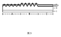
図1に示すように、光学偽造防止素子について、第1領域を画像領域A、第2領域を透かし領域B、第3領域を干渉光学的変色領域Cとする。画像領域Aは高輝度反射微細構造(例えば、ホログラフィック又は非回折光学微細構造)の光学特徴を有し、一般には、特定の画像、例えば、図中の「PY」アルファベットで示される。干渉光学的変色領域Cに対して反射観察を行う場合、異なる角度から異なる色が見られる。透かし領域Cに対して透視観察を行う場合、透光又は半透光効果を有する。透かし領域Cと画像領域Aは厳密に位置決めされ、誤差がなく、例えば、図1中の透かし領域Cは画像領域Aの境界を厳密に囲み、画像の輪郭で示される。透かし領域の精細度は非常に高くてもよく、例えば、10umよりも小さくてもよい。 As shown in FIG. 1, in the optical anti-counterfeiting element, the first region is an image region A, the second region is a watermark region B, and the third region is an interference optical discoloration region C. Image area A has optical features of high brightness reflective microstructures (eg, holographic or non-diffractive optical features) and is generally designated by a particular image, eg, the "PY" alphabet in the figures. When reflective observation is performed on the interference optical color change area C, different colors are seen from different angles. When transparent observation is performed on the watermark area C, it has a transparent or semi-transparent effect. The watermark area C and the image area A are precisely positioned and without errors; for example, the watermark area C in FIG. 1 strictly surrounds the boundary of the image area A and is indicated by the outline of the image. The definition of the watermark area may be very high, for example smaller than 10 um.
図2は図1に示す例示的な光学偽造防止素子のX-Xに沿う可能な断面図である。光学偽造防止素子は基材1、レリーフ構造層2、干渉光学的変色層3(反射層31、誘電体層32、及び吸収層33を含む)、及びほかの機能コーティング4を備える。レリーフ構造層2は、比体積の小さい第1微細構造から構成される第1領域A、比体積の大きい第2微細構造から構成される第2領域B、及び平坦なレリーフ構造無し第3領域Cを含む。第1領域A及び第2領域Bはいずれも反射層31、誘電体層32及び吸収層33を有するが、第2領域Bは反射層31、誘電体層32及び吸収層33を有しない。
FIG. 2 is a possible cross-sectional view along XX of the exemplary optical anti-counterfeiting element shown in FIG. The optical anti-counterfeiting element comprises a
誘電体層32はプリントによって形成されるため、第1領域Aの誘電体層32はレリーフ構造層2及び反射層3に異型被覆され、その結果、反射層31と吸収層33の間に効果的なファブリペロー共振器が形成されておらず、即ち、第1領域Aは干渉光学的変色効果を示していない、又は弱い干渉光学的変色効果を示す。
Since the dielectric layer 32 is formed by printing, the dielectric layer 32 in the first area A is coated with a profile on the
一方、第3領域Cのレリーフ構造層2は平坦構造であり、反射層31と吸収層33の間に効果的なファブリペロー共振器が形成され、従って、明らかな干渉光学的変色効果を示す。第2領域Bは反射層31、誘電体層32及び吸収層33を有しないため、透視観察を行うと、高透明な透かし効果を示す。ほかの機能コーティング5は必要に応じて設置でき、例えば、接着層として、保護される主製品との接着の役割を果たす。
Meanwhile, the
図3は図1に示す例示的な光学偽造防止素子のX-Xに沿う別の可能な断面図である。光学偽造防止素子は基材1、レリーフ構造層2、干渉光学的変色層3(反射層31、誘電体層32、及び吸収層33を含む)、保護層5、及びほかの機能コーティング4を備える。図2と同様に、レリーフ構造層2は比体積の小さい第1微細構造から構成される第1領域A、比体積の大きい第2微細構造から構成される第2領域B、及び平坦なレリーフ構造無し第3領域Cを含む。
FIG. 3 is another possible cross-sectional view along XX of the exemplary optical anti-counterfeiting element shown in FIG. The optical anti-counterfeiting element comprises a
一方、図2との相違点として、吸収層33はレリーフ構造層2と隣接し、且つ第2領域Bは反射層31を有しないが、誘電体層32及び吸収層33を有する。吸収層33が存在するため、第2領域Bに対して透視観察を行う場合、半透光の透かし効果を示す。保護層5は製造過程で第1領域A及び第3領域C上の反射層31を保護することにより導入される。
On the other hand, as a difference from FIG. 2, the absorbing layer 33 is adjacent to the
以下、図4を参照しながら本発明に係る図2に示す光学偽造防止素子の製造方法を説明し、該方法はステップS11~S13を含む。 Hereinafter, a method for manufacturing the optical counterfeit prevention element shown in FIG. 2 according to the present invention will be described with reference to FIG. 4, and the method includes steps S11 to S13.
S11、図4に示すように、基材1上にレリーフ構造層2を形成し、前記レリーフ構造層2は少なくとも、比体積の小さい第1微細構造から構成される第1領域A、比体積の大きい第2微細構造から構成される第2領域B、及び平坦な構造無し第3領域Cを含む。
S11, as shown in FIG. 4, a
基材1は少なくとも部分的に透明的であってもよく、色付きの誘電体層であってもよく、表面に機能コーティングを有する透明誘電体薄膜であってもよく、複合した多層膜であってもよい。基材1は一般には、物理的及び化学的耐性に優れ機械的強度が高い薄膜材料で形成され、例えば、ポリエチレンテレフタレート(PET)薄膜、ポリエチレンナフタレート(PEN)薄膜及びプロピレン(PP)薄膜等のプラスチック薄膜を使用して基材1を形成してもよく、且つ基材1は好ましくはPET材料で形成される。基材1とレリーフ構造層2の接着を強化するように、基材1上に接着強化層を含んでもよい。
The
レリーフ構造層2は紫外線鋳造、型鍛造、ナノインプリント等の加工方式によってバッチ複製して形成されてもよい。例えば、レリーフ構造層2は熱可塑性樹脂で型鍛造プロセスによって形成されてもよく、即ち、基材1上に事前に塗布された熱可塑性樹脂が高温の金属ダイプレートを通過するとき、加熱されて軟化して変形し、それにより特定のレリーフ構造を形成し、その後、冷却成形する。レリーフ構造層2は放射線硬化鋳造プロセスを用いて形成されてもよく、即ち、放射線硬化性樹脂を基材1上に塗布し、型板をそれに押し当てながら紫外線又は電子ビーム等の放射線を照射し、上記材料を硬化させ、その後、型板を取り外してレリーフ構造層2を形成する。
The
前記レリーフ構造層2は比体積の小さい第1微細構造から構成される第1領域A、比体積の大きい第2微細構造から構成される第2領域B、及び平坦な構造無し第3領域Cを含む。第1微細構造は周期的構造又は非周期的構造のうちの1種又は組み合わせであってもよく、横断面構造は正弦型構造、矩形格子構造、半円形構造、及びブレーズド格子構造のうちの1種又は組み合わせであってもよい。第1微細構造の具体的なサイズ(例えば、周期、深さ等)は形成される必要がある光学効果に応じて決定される。
The
一般には、特定の光学効果及び後続の透かし工程の需要を満たすために、前記第1微細構造の比体積は0.05um3/um2よりも大きく0.5um3/um2よりも小さい必要があり、より好ましくは、0.1um3/um2よりも大きく0.3um3/um2よりも小さい。第2微細構造は周期的構造又は非周期的構造のうちの1種又は組み合わせであってもよく、横断面構造は正弦型構造、矩形格子構造、半円形構造、台形構造、及びブレーズド格子構造のうちの1種又は組み合わせであってもよい。 Generally, the specific volume of the first microstructure needs to be greater than 0.05 um 3 /um 2 and smaller than 0.5 um 3 /um 2 to meet the demands of specific optical effects and subsequent watermarking processes . More preferably, it is larger than 0.1 um 3 /um 2 and smaller than 0.3 um 3 /um 2 . The second microstructure may be one or a combination of a periodic structure or an aperiodic structure, and the cross-sectional structure may be a sinusoidal structure, a rectangular lattice structure, a semicircular structure, a trapezoidal structure, and a blazed lattice structure. It may be one type or a combination of them.
第2微細構造は完全に透かしに使用され、最終的な製品では光学効果を形成しないため、透かしの需要に応じて微細構造の形状を設計できる。通常、微細構造の比体積は大きいほど、透かしに有利である。 The second microstructure is completely used for the watermark and does not form any optical effect in the final product, so the shape of the microstructure can be designed according to the watermark demand. Generally, the larger the specific volume of the microstructure, the more advantageous it is to watermarking.
一方、微細構造の比体積は大きいほど、微細構造は広く且つ深く、量産の難度は高い。好ましくは、前記第2微細構造の比体積は0.1um3/um2よりも大きく1um3/um2よりも小さく、より好ましくは、0.2um3/um2よりも大きく0.5um3/um2よりも小さい。 On the other hand, the larger the specific volume of the microstructure, the wider and deeper the microstructure, and the higher the difficulty of mass production. Preferably, the specific volume of the second microstructure is greater than 0.1 um 3 /um 2 and less than 1 um 3 /um 2 , more preferably greater than 0.2 um 3 /um 2 and 0.5 um 3 /. um smaller than 2 .
S12、図5に示すように、レリーフ構造層2上に反射層31、誘電体層32及び吸収層33を順に形成し、反射層31及び吸収層33は気相成長によって形成され、誘電体層32はプリントによって形成される。
S12, as shown in FIG. 5, a reflective layer 31, a dielectric layer 32, and an absorbing layer 33 are sequentially formed on the
反射層31は強い反射作用を持つ必要があり、一般には、高反射率の金属メッキ層を使用し、単層金属メッキ層、又は多層金属メッキ層、又は多金属混合メッキ層であってもよい。反射層の材料はAl、Cu、Ni、Cr、Ag、Fe、Sn、Au、及びPt等の金属又はその混合物又は合金であってもよく、アルミニウムは、低コスト及び高輝度のため、好ましい。反射層31は気相成長方法によってレリーフ構造層2上に形成され、例えば、熱蒸着、マグネトロンスパッタリング等を含むが、これらに限定されない。
The reflective layer 31 must have a strong reflective effect, and generally uses a metal plating layer with high reflectance, and may be a single metal plating layer, a multilayer metal plating layer, or a multimetal mixed plating layer. . The material of the reflective layer may be metals such as Al, Cu, Ni, Cr, Ag, Fe, Sn, Au, and Pt, or mixtures or alloys thereof, with aluminum being preferred due to its low cost and high brightness. The reflective layer 31 is formed on the
好ましくは、反射層31は均一な表面密度でレリーフ構造層2上に同型被覆又は略同型被覆の方式で形成される。反射層の厚さは一般には、10nmよりも大きく80nmよりも小さく、好ましくは20nmよりも大きく50nmよりも小さい。反射層は薄すぎると、輝度不足となり、反射層は厚すぎると、レリーフ構造層との接着性が低く、且つコストが高くなる。
Preferably, the reflective layer 31 is formed on the
誘電体層32はプリントプロセスによって実現される。ここでのプリントとは、液体ワニスを施した薄膜を乾燥して硬化させるプロセスであり、形成領域という点から、薄膜の全領域に形成されてもよく(塗布プロセスという)、薄膜の部分領域に形成されてもよく(印刷プロセスという)、具体的な実施技術という点から、スプレー、ロール塗布、フレキソ印刷、グラビア印刷、シルクスクリーン印刷等が挙げられる。 Dielectric layer 32 is realized by a printing process. Printing here refers to the process of drying and curing a thin film coated with liquid varnish, and in terms of the forming area, it may be printed on the entire area of the thin film (referred to as a coating process), or it may be printed on a partial area of the thin film. In terms of specific implementation techniques, mention may be made of spraying, roll coating, flexographic printing, gravure printing, silk screen printing, etc.
このようなプロセスによって、第1領域Aの誘電体層の表面が反射層31に異型被覆され、それにより吸収層を最終的に形成した後、干渉光学的変色特徴がない、又は干渉光学的変色特徴が弱い。誘電体層32は以下の透かし工程における保護層の作用を同時に提供する。誘電体層32のプリント量は、第1領域Aの反射層31の最小厚さが第2領域Bの反射層31の最小厚さよりも遥かに小さいように設定されるべきである。一般には、コーティングの最小厚さは微細構造の最上部にある。 Through this process, the surface of the dielectric layer in the first region A is coated with the reflective layer 31, so that after the final formation of the absorbing layer, there is no interference optical color change feature or there is no interference optical color change feature. Characteristics are weak. The dielectric layer 32 also serves as a protective layer in the following watermarking process. The printing amount of the dielectric layer 32 should be set such that the minimum thickness of the reflective layer 31 in the first region A is much smaller than the minimum thickness of the reflective layer 31 in the second region B. Generally, the minimum thickness of the coating is at the top of the microstructure.
このように、後述する透かし工程では、反射層材料と反応可能な腐食雰囲気において、誘電体層は第1領域Aの反射層に対する効果的な保護を提供できるが、第2領域Bの反射層に対する効果的な保護を提供できない。誘電体層の主樹脂はポリウレタン、アクリル酸、ポリエステル又はそれらの組み合わせからなるようにしてもよい。 Thus, in the watermarking process described below, the dielectric layer can provide effective protection for the reflective layer in the first region A, but not for the reflective layer in the second region B, in a corrosive atmosphere that can react with the reflective layer material. Failure to provide effective protection. The main resin of the dielectric layer may be made of polyurethane, acrylic acid, polyester, or a combination thereof.
第3領域Cは干渉光学的変色領域として、誘電体層の表面が平坦であるほど、効果的なファブリペロー共振器の形成に有利である。従って、誘電体層はプリント前、非常に低い粘度を有するべきであり、例えば、20cps未満であり、このように、反射層上によりよくレベリングできる。ほとんどの樹脂の場合、屈折率はいずれも1.5程度であり、良好な光学的変色効果を図るために、誘電体層のプリント厚さは200nm~800nm範囲内にあるべきである。その具体的な厚さは所要の色及び透かしの条件に応じて共同で決定されるべきである。 The third region C serves as an interference optical color change region, and the flatter the surface of the dielectric layer, the more advantageous it is to forming an effective Fabry-Perot resonator. Therefore, the dielectric layer should have a very low viscosity before printing, eg less than 20 cps, thus allowing better leveling onto the reflective layer. For most resins, the refractive index is around 1.5, and the printed thickness of the dielectric layer should be in the range of 200 nm to 800 nm for good optical color change effect. Its specific thickness should be determined jointly depending on the required color and watermark requirements.
吸収層33の材料はAl、Cu、Ni、Cr、Ag、Fe、Sn、Au、Pt等の金属又はこれらの混合物又は合金であってもよく、ニッケル又はクロムは非常に薄い状態でも化学的安定性が高く且つコストが非常に低いため、好ましい。吸収層33は気相成長方法によって形成され、例えば、熱蒸着、マグネトロンスパッタリング等を含むが、これらに限定されない。好ましくは、吸収層33は均一な表面密度で同型被覆又は略同型被覆の方式で誘電体層32上に形成される。 The material of the absorption layer 33 may be a metal such as Al, Cu, Ni, Cr, Ag, Fe, Sn, Au, Pt, or a mixture or alloy thereof, and nickel or chromium is chemically stable even in a very thin state. It is preferable because it has high properties and very low cost. The absorption layer 33 is formed by a vapor deposition method, including, but not limited to, thermal evaporation, magnetron sputtering, and the like. Preferably, the absorbing layer 33 is formed on the dielectric layer 32 in a homogeneous or substantially homogeneous manner with a uniform surface density.
吸収層の厚さは一般には薄く、一般には、10nmよりも小さい。吸収層が薄すぎると、光学的変色効果が悪く、吸収層が厚すぎると、色が暗すぎる。吸収層の厚さに対応する透光率は一般には、10%よりも大きく80%よりも小さく、好ましくは、20%よりも大きく50%よりも小さい。 The thickness of the absorbing layer is generally thin, typically less than 10 nm. If the absorption layer is too thin, the optical color change effect will be poor, and if the absorption layer is too thick, the color will be too dark. The light transmission, which corresponds to the thickness of the absorption layer, is generally greater than 10% and less than 80%, preferably greater than 20% and less than 50%.
S13、図6に示すように、第2領域Bの反射層31が完全に又は部分的に除去されるまで、半製品を反射層材料31と反応可能な腐食雰囲気に配置する。 S13, as shown in FIG. 6, the semi-finished product is placed in a corrosive atmosphere capable of reacting with the reflective layer material 31 until the reflective layer 31 in the second area B is completely or partially removed.
上記したように、誘電体層32のプリント量は、第1領域Aの反射層31の最小厚さが第2領域Bの反射層31の最小厚さよりも遥かに小さいように設定される。吸収層の厚さが非常に小さいため、反射層に対する保護作用をほぼ提供しない。従って、誘電体層は第1領域Aの反射層に対する効果的な保護を提供できるが、第2領域Bの反射層に対する効果的な保護を提供できない。 As described above, the printing amount of the dielectric layer 32 is set so that the minimum thickness of the reflective layer 31 in the first region A is much smaller than the minimum thickness of the reflective layer 31 in the second region B. The thickness of the absorbing layer is so small that it provides almost no protection for the reflective layer. Therefore, the dielectric layer can provide effective protection for the reflective layer in the first region A, but cannot provide effective protection for the reflective layer in the second region B.
反射層の材料と反応可能な腐食雰囲気において、所定時間後、第2領域Bの反射層が腐食除去されるが、第1領域Aの反射層が腐食されていない、又はほぼ腐食されていない。勿論、第3領域Cに微細構造がないため、誘電体層の厚さが一致し、厚さが非常に大きく、腐食雰囲気において反射層を効果的に保護できる。 After a predetermined time in a corrosive atmosphere that can react with the material of the reflective layer, the reflective layer in the second area B is corroded and removed, but the reflective layer in the first area A is not corroded or is almost not corroded. Of course, since there is no microstructure in the third region C, the thickness of the dielectric layer is consistent and the thickness is very large, which can effectively protect the reflective layer in a corrosive atmosphere.
一般には、第2領域Bの反射層が除去された後、その上の誘電体層及び吸収層もリフトオフされる。ここまで、図2に示す光学偽造防止素子の光学効果が形成され、吸収層側から反射観察を行う場合、第1領域Aは微細構造による光学偽造防止特徴を有するが、干渉光学的変色特徴がない、又は干渉光学的変色特徴が弱いことに対して、第3領域Cは明らかな干渉光学的変色特徴を有するが、微細構造の光学特徴を有せず、透視観察を行う場合、第2領域Bは透光透かし特徴を有する。 Generally, after the reflective layer in the second region B is removed, the overlying dielectric layer and absorption layer are also lifted off. Up to this point, the optical effect of the optical anti-counterfeiting element shown in FIG. 2 has been formed, and when performing reflective observation from the absorption layer side, the first area A has the optical anti-counterfeiting feature due to the fine structure, but the interference optical discoloration feature is In contrast, the third region C has clear interference optical color change characteristics but does not have fine structure optical features, and when performing perspective observation, the second region C has no interference optical color change characteristics. B has a translucent watermark feature.
図2に示す光学偽造防止素子の製造方法は、図7に示すように、一般には、ステップS13の後、ほかの機能コーティングをプリントするステップをさらに含み、例えば、接着層を形成し、被保護製品との接着の作用を発揮する。 As shown in FIG. 7, the method for manufacturing the optical anti-counterfeiting element shown in FIG. 2 generally further includes printing other functional coatings after step S13, such as forming an adhesive layer and Demonstrates adhesion to the product.
(実施例2)
以下、図5を参照しながら本発明に係る図2に示す光学偽造防止素子の製造方法を説明し、該方法はステップS21~S24を含んでもよい。
(Example 2)
Hereinafter, a method for manufacturing the optical anti-counterfeiting element shown in FIG. 2 according to the present invention will be described with reference to FIG. 5, and the method may include steps S21 to S24.
S21、図8に示すように、基材1上にレリーフ構造層2を形成し、前記レリーフ構造層2は少なくとも、比体積の小さい第1微細構造から構成される第1領域A、比体積の大きい第2微細構造から構成される第2領域B、及び平坦な構造無し第3領域Cを含む。
S21, as shown in FIG. 8, a
ここでの基材、レリーフ構造層の要件はステップS11と完全に同様である。ここでは詳細説明を省略する。 The requirements for the base material and the relief structure layer here are completely the same as in step S11. Detailed explanation will be omitted here.
S22、図9に示すように、レリーフ構造層2上に吸収層33、誘電体層32及び反射層31を順に形成し、反射層31及び吸収層33は気相成長によって形成され、誘電体層32はプリントによって形成される。
S22, as shown in FIG. 9, an absorption layer 33, a dielectric layer 32 and a reflection layer 31 are formed in this order on the
ここで、吸収層、誘電体層、反射層の形成順序はS12と異なる。このような形成順序によって、後続の反射層の透かし工程では、反射層のみを除去し、吸収層の誘電体層を除去しない。誘電体層の作用は単に干渉光学的変色特徴を提供することであり、透かし工程におけるメッキ層に対する保護作用を有しない。従って、誘電体層の厚さ設定は主に第3領域Cの形成に必要な干渉光学的変色色特徴に応じて決定されてもよい。また、誘電体層の厚さは、後続の透かしの需要を満たすために、誘電体層の表面が依然として大きな比体積を確保するように設定すべきである。 Here, the order of formation of the absorbing layer, dielectric layer, and reflective layer is different from S12. Due to this formation order, in the subsequent watermarking process of the reflective layer, only the reflective layer is removed and the dielectric layer of the absorbing layer is not removed. The function of the dielectric layer is simply to provide an interferometric optical color change feature and has no protective effect on the plating layer during the watermarking process. Therefore, the thickness setting of the dielectric layer may be determined mainly depending on the interference optical discoloration color characteristics required for forming the third region C. Also, the thickness of the dielectric layer should be set so that the surface of the dielectric layer still has a large specific volume to meet the subsequent watermark demands.
吸収層及び反射層の材料及びプロセスの要件はステップS12と完全に同様である。ここでは詳細説明を省略する。 The material and process requirements for the absorbing and reflective layers are completely similar to step S12. Detailed explanation will be omitted here.
S23、図10に示すように、反射層上に保護層プリント工程を施し、前記保護層の第1領域の最小厚さは第2領域の最小厚さよりも遥かに大きい。 S23, as shown in FIG. 10, a protective layer printing process is performed on the reflective layer, and the minimum thickness of the first region of the protective layer is much larger than the minimum thickness of the second region.
保護層5は透かし工程における第1領域Aと第3領域Cの反射層に対する保護作用を提供する。従って、保護層5のプリント量は、第1領域Aの反射層31の最小厚さが第2領域Bの反射層31の最小厚さよりも遥かに小さいように設定されるべきである。一般には、コーティングの最小厚さは微細構造の最上部にある。このように、後述する透かし工程では、反射層31の材料と反応可能な腐食雰囲気において、保護層5は第1領域Aと第3領域Cの反射層に対する効果的な保護を提供できるが、第2領域Bの反射層に対する効果的な保護を提供できない。保護層5の主樹脂はポリウレタン、アクリル酸、ポリエステル又はこれらの組み合わせから構成されてもよい。
The
S24、図11に示すように、第2領域の反射層が完全に又は部分的に除去されるまで、半製品を反射層の材料と反応可能な腐食雰囲気に配置する。 S24, as shown in FIG. 11, the semi-finished product is placed in a corrosive atmosphere capable of reacting with the material of the reflective layer until the reflective layer in the second area is completely or partially removed.
反射層31の材料と反応可能な腐食雰囲気において、所定時間後、第2領域Bの反射層は腐食除去されるが、第1領域Aと第3領域Cの反射層は腐食されていない、又はほぼ腐食されていない。このとき、第2領域Bの反射層が除去された後、その上の保護層もリフトオフされるが、誘電体層及び吸収層は一般には除去されない。 In a corrosive atmosphere that can react with the material of the reflective layer 31, after a predetermined period of time, the reflective layer in the second area B is corroded and removed, but the reflective layers in the first area A and the third area C are not corroded, or Almost no corrosion. At this time, after the reflective layer in the second region B is removed, the protective layer thereon is also lifted off, but the dielectric layer and the absorbing layer are generally not removed.
しかし、吸収層も腐食雰囲気と反応可能な場合、誘電体層及び吸収層も除去可能である。ここまで、図3に示す光学偽造防止素子の光学効果が形成され、吸収層側から反射観察を行う場合、第1領域Aは微細構造による光学偽造防止特徴を有するが、干渉光学的変色特徴がない、又は干渉光学的変色特徴が弱いことに対して、第3領域Cは明らかな干渉光学的変色特徴を有するが、微細構造の光学特徴を有せず、透視観察を行う場合、第2領域Bは透光透かし特徴を有する。 However, if the absorption layer is also capable of reacting with the corrosive atmosphere, the dielectric layer and the absorption layer can also be removed. Up to this point, the optical effect of the optical anti-counterfeiting element shown in FIG. 3 has been formed, and when performing reflective observation from the absorption layer side, the first area A has the optical anti-counterfeiting feature due to the fine structure, but the interference optical discoloration feature is In contrast, the third region C has clear interference optical color change characteristics but does not have fine structure optical features, and when performing perspective observation, the second region C has no interference optical color change characteristics. B has a translucent watermark feature.
図3に示す光学偽造防止素子の製造方法は、図12に示すように、一般には、ステップS24の後、ほかの機能コーティングをプリントするステップをさらに含み、例えば、接着層を形成し、被保護製品との接着の作用を発揮する。 As shown in FIG. 12, the method for manufacturing the optical anti-counterfeiting element shown in FIG. 3 generally further includes printing other functional coatings after step S24, for example, forming an adhesive layer and Demonstrates adhesion to the product.
本発明に係る光学偽造防止素子の製造方法は、孔付き安全線、ラベル、ロゴ、太い安全線、透明窓、被覆膜等の製造に適する。前記孔付き安全線を備えた偽造防止紙は紙幣、パスポート、有価証券等の様々な高セキュリティ製品の偽造防止に使用される。 The method for manufacturing an optical anti-counterfeiting element according to the present invention is suitable for manufacturing safety wires with holes, labels, logos, thick safety wires, transparent windows, coating films, and the like. The anti-counterfeit paper with the perforated security line is used to prevent counterfeiting of various high-security products such as banknotes, passports, and securities.
以上、図面を参照しながら本発明の実施例の選択可能な実施形態を詳細に説明したが、本発明の実施例は上記実施形態の詳細に限定されるものではなく、本発明の実施例の技術的概念の範囲内で、本発明の実施例の技術案に対して種々の簡単な変形を行うことができ、これらの簡単な変形はすべて本発明の実施例の保護範囲に属する。 Although selectable embodiments of the embodiments of the present invention have been described in detail with reference to the drawings, the embodiments of the present invention are not limited to the details of the embodiments described above, and the embodiments of the present invention are not limited to the details of the embodiments. Within the scope of the technical concept, various simple modifications can be made to the technical solution of the embodiments of the present invention, and all these simple modifications fall within the protection scope of the embodiments of the present invention.
またなお、上記具体的な実施形態で説明された各具体的な技術的特徴は、矛盾しない限り、任意に適宜組み合わせることができる。不必要な重複を回避するために、本発明の実施例は種々の可能な組み合わせ方式を別途説明しない。 Further, the specific technical features described in the above specific embodiments can be arbitrarily and appropriately combined as long as they do not contradict each other. To avoid unnecessary duplication, the embodiments of the present invention do not separately describe various possible combination schemes.
当業者であれば、上記実施例の方法の全部又は一部のステップをプログラムによって関連ハードウェアに命令を出して完了させることができると理解でき、該プログラムは1つの記憶媒体に記憶されており、複数の命令を含み、シングルチップマイコン、チップ又はプロセッサ(processor)に本願の各実施例に記載の方法の全部又は一部のステップを実行させる。上記記憶媒体は、Uディスク、モバイルハードディスク、読み取り専用メモリ(ROM、Read-OnlyMemory)、ランダムアクセスメモリ(RAM、RandomAccessMemory)、磁気ディスク又は光ディスクなどプログラムコードを記憶できる様々な媒体を含む。 Those skilled in the art will understand that all or some of the steps of the method of the above embodiments can be completed by issuing instructions to related hardware by a program, and the program is stored in a single storage medium. , a plurality of instructions, and causes a single-chip microcomputer, chip, or processor to execute all or some steps of the method described in each embodiment of the present application. The storage medium includes various media capable of storing program codes, such as a U disk, a mobile hard disk, a read-only memory (ROM), a random access memory (RAM), a magnetic disk, or an optical disk.
また、本発明の実施例の様々な実施形態は任意に組み合わせることができ、本発明の実施例の思想を逸脱しない限り、同様に本発明の実施例に開示されるものとみなすべきである。 Moreover, various embodiments of the embodiments of the present invention can be arbitrarily combined and should be considered to be similarly disclosed in the embodiments of the present invention unless they depart from the spirit of the embodiments of the present invention.
A…画像領域、B…透かし領域、C…干渉光学的変色領域、1…基材、2…レリーフ構造層、3…干渉光学的変色層、31…反射層、32…誘電体層、33…吸収層、4…ほかの機能コーティング。 A...Image area, B...Watermark area, C...Interference optical color change area, 1...Base material, 2...Relief structure layer, 3...Interference optical color change layer, 31...Reflection layer, 32...Dielectric layer, 33... Absorption layer, 4...Other functional coatings.
Claims (17)
第1領域、第2領域及び第3領域を有するレリーフ構造層を備え、前記第1領域は第1微細構造を有し、前記第2領域は第2微細構造を有し、前記第3領域は構造無し平坦領域であり、
前記第2微細構造の比体積は前記第1微細構造の比体積よりも大きく、
前記第1領域及び前記第3領域に対応する位置のいずれかにも重なる反射層、誘電体層及び吸収層が設けられており、前記第2領域は反射層を有せず、前記第2領域は透かし領域であり、前記第2領域は前記第1領域と前記第3領域との間に位置し、
前記誘電体層はプリントによって形成され、前記第1領域に対応する誘電体層の前記レリーフ構造層側から離れた表面形態は前記レリーフ構造層の表面形態と明らかに異なることを特徴とする光学偽造防止素子。 An optical anti-counterfeiting element,
a relief structure layer having a first region, a second region and a third region, the first region having a first microstructure, the second region having a second microstructure, and the third region having a first microstructure; It is a flat area without structure,
The specific volume of the second microstructure is larger than the specific volume of the first microstructure,
A reflective layer, a dielectric layer, and an absorbing layer are provided at positions corresponding to the first region and the third region, and the second region does not have a reflective layer, and the second region does not have a reflective layer. is a watermark area, the second area is located between the first area and the third area,
The dielectric layer is formed by printing, and the surface morphology of the dielectric layer corresponding to the first region away from the relief structure layer side is clearly different from the surface morphology of the relief structure layer. Prevention element.
前記第1微細構造の延在方向に沿う横断面構造は、正弦型構造、矩形格子構造、半円形構造、及びブレーズド格子構造のうちの1種の構造、又は正弦型構造、矩形格子構造、半円形構造、及びブレーズド格子構造のうちの少なくとも任意の2種の構造を組み合わせた構造であることを特徴とする請求項1に記載の光学偽造防止素子。 The first fine structure is one of a periodic structure and a non-periodic structure, or a combination of a periodic structure and a non-periodic structure,
The cross-sectional structure along the extending direction of the first microstructure is one of a sine type structure, a rectangular lattice structure, a semicircular structure, and a blazed lattice structure, or a sine type structure, a rectangular lattice structure, and a semicircular lattice structure. The optical anti-counterfeiting element according to claim 1, characterized in that it has a structure that combines at least two types of structures of a circular structure and a blazed lattice structure.
前記第2微細構造の延在方向に沿う横断面構造は、正弦型構造、矩形格子構造、半円形構造、台形構造、及びブレーズド格子構造のうちの1種の構造、又は正弦型構造、矩形格子構造、半円形構造、台形構造、及びブレーズド格子構造のうちの少なくとも任意の2種の構造を組み合わせた構造であることを特徴とする請求項1に記載の光学偽造防止素子。 The second fine structure is one of a periodic structure and a non-periodic structure, or a combination of a periodic structure and a non-periodic structure,
The cross-sectional structure along the extending direction of the second microstructure is one of a sine type structure, a rectangular lattice structure, a semicircular structure, a trapezoidal structure, and a blazed lattice structure, or a sine type structure, a rectangular lattice structure. 2. The optical anti-counterfeiting element according to claim 1, wherein the optical forgery prevention element has a structure that is a combination of at least two types of structures selected from the group consisting of a semicircular structure, a trapezoidal structure, a blazed lattice structure, and a blazed lattice structure.
前記誘電体層の主樹脂は、ポリウレタン、アクリル酸、及びポリエステルのうちの1種の樹脂、又はポリウレタン、アクリル酸、及びポリエステルのうちの少なくとも任意の2種の樹脂を組み合わせたポリマーを含み、
前記吸収層の材料は、ニッケル、クロム、アルミニウム、銀、銅、錫、及びチタンのうちの1種の金属、又はニッケル、クロム、アルミニウム、銀、銅、錫、及びチタンのうちの少なくとも任意の2種の金属を組み合わせた合金を含むことを特徴とする請求項1に記載の光学偽造防止素子。 The material of the reflective layer is one of aluminum, silver, copper, tin, chromium, nickel, and titanium, or at least any one of aluminum, silver, copper, tin, chromium, nickel, and titanium. Contains alloys that combine two types of metals,
The main resin of the dielectric layer includes one resin selected from polyurethane, acrylic acid, and polyester, or a combination of at least two resins selected from polyurethane, acrylic acid, and polyester,
The material of the absorption layer is one of nickel, chromium, aluminum, silver, copper, tin, and titanium, or at least any one of nickel, chromium, aluminum, silver, copper, tin, and titanium. The optical anti-counterfeiting element according to claim 1, characterized in that it contains an alloy that is a combination of two types of metals.
第1領域、第2領域及び第3領域を有し、前記第1領域が第1微細構造を有し、前記第2領域が第2微細構造を有し、前記第2微細構造の比体積が前記第1微細構造の比体積よりも大きく、前記第3領域が構造無し平坦領域であり、前記第2領域が前記第1領域と前記第3領域との間に位置するレリーフ構造層を形成するステップS1)と、
前記レリーフ構造層上に反射層、誘電体層及び吸収層を順に形成し、気相成長によって反射層を形成し、プリントによって誘電体層を形成し、気相成長によって吸収層を形成するステップS2)と、
透かし領域である第2領域に対応する位置における反射層が完全に又は部分的に除去されるまで、ステップS2)の半製品を反射層の材料と反応可能な腐食雰囲気に配置するステップS3)と、を含むことを特徴とする光学偽造防止素子の製造方法。 A method for manufacturing an optical anti-counterfeiting element, comprising:
a first region, a second region, and a third region, the first region has a first microstructure, the second region has a second microstructure, and the specific volume of the second microstructure is forming a relief structure layer that is larger than the specific volume of the first microstructure, the third region is a structure-free flat region, and the second region is located between the first region and the third region. Step S1) and
Step S2 of sequentially forming a reflective layer, a dielectric layer, and an absorbing layer on the relief structure layer, forming the reflective layer by vapor phase growth, forming the dielectric layer by printing, and forming the absorbing layer by vapor phase growth. )and,
step S3) of placing the semi-finished product of step S2) in a corrosive atmosphere capable of reacting with the material of the reflective layer until the reflective layer at the location corresponding to the second area, which is the watermark area, is completely or partially removed; A method for manufacturing an optical anti-counterfeiting element, comprising:
前記第2領域に対応する位置における誘電体層及び吸収層も完全に又は部分的に除去されるステップをさらに含むことを特徴とする請求項13に記載の製造方法。 In step S3), the process of completely or partially removing the reflective layer at the position corresponding to the second area includes:
14. The manufacturing method according to claim 13, further comprising the step of also completely or partially removing the dielectric layer and the absorption layer at positions corresponding to the second region.
第1領域、第2領域及び第3領域を有し、前記第1領域が第1微細構造を有し、前記第2領域が第2微細構造を有し、前記第2微細構造の比体積が前記第1微細構造の比体積よりも大きく、前記第3領域が構造無し平坦領域であり、前記第2領域が前記第1領域と前記第3領域との間に位置するレリーフ構造層を形成するステップS1)と、
前記レリーフ構造層上に吸収層、誘電体層及び反射層を順に形成し、気相成長によって反射層を形成し、プリントによって誘電体層を形成し、気相成長によって吸収層を形成するステップS2)と、
前記反射層を形成した後、異なる厚さ方式でプリント工程を施して保護層を形成し、前記異なる厚さ方式は前記第1領域の保護層の最小厚さが前記第2領域の保護層の最小厚さよりも遥かに大きい方式であるステップS3)と、
透かし領域である前記第2領域に対応する位置における反射層が完全に又は部分的に除去されるまで、ステップS3)の半製品を前記反射層の材料と反応可能な腐食雰囲気に配置して反射防止処理を行うステップS4)と、を含むことを特徴とする光学偽造防止素子の製造方法。 A method for manufacturing an optical anti-counterfeiting element, comprising:
a first region, a second region, and a third region, the first region has a first microstructure, the second region has a second microstructure, and the specific volume of the second microstructure is forming a relief structure layer that is larger than the specific volume of the first microstructure, the third region is a structure-free flat region, and the second region is located between the first region and the third region. Step S1) and
Step S2 of sequentially forming an absorbing layer, a dielectric layer, and a reflective layer on the relief structure layer, forming a reflective layer by vapor phase growth, forming a dielectric layer by printing, and forming an absorbing layer by vapor phase growth. )and,
After forming the reflective layer, a printing process is performed to form a protective layer using different thickness methods, and the different thickness methods are such that the minimum thickness of the protective layer in the first area is the same as that of the protective layer in the second area. Step S3), which is much larger than the minimum thickness;
The semi-finished product of step S3) is placed in a corrosive atmosphere capable of reacting with the material of the reflective layer until the reflective layer at the position corresponding to the second area, which is the watermark area, is completely or partially removed. A method for manufacturing an optical forgery prevention element, comprising: step S4) of performing a prevention process.
前記第2領域の反射層が除去され、誘電体層及び吸収層がいずれも除去されていないステップをさらに含むことを特徴とする請求項15に記載の製造方法。 In step S4), the process of completely or partially removing the reflective layer at the position corresponding to the second area includes:
16. The method of claim 15, further comprising removing the reflective layer in the second region, but leaving neither the dielectric layer nor the absorbing layer removed.
Applications Claiming Priority (3)
| Application Number | Priority Date | Filing Date | Title |
|---|---|---|---|
| CN201910251304.8 | 2019-03-29 | ||
| CN201910251304.8A CN111746171B (en) | 2019-03-29 | 2019-03-29 | Optical anti-counterfeiting element and manufacturing method thereof |
| PCT/CN2020/081592 WO2020200070A1 (en) | 2019-03-29 | 2020-03-27 | Optical anti-counterfeiting element and manufacturing method therefor |
Publications (2)
| Publication Number | Publication Date |
|---|---|
| JP2022525371A JP2022525371A (en) | 2022-05-12 |
| JP7417625B2 true JP7417625B2 (en) | 2024-01-18 |
Family
ID=72664531
Family Applications (1)
| Application Number | Title | Priority Date | Filing Date |
|---|---|---|---|
| JP2021555864A Active JP7417625B2 (en) | 2019-03-29 | 2020-03-27 | Optical anti-counterfeiting element and its manufacturing method |
Country Status (5)
| Country | Link |
|---|---|
| US (1) | US12304231B2 (en) |
| EP (1) | EP3950372A4 (en) |
| JP (1) | JP7417625B2 (en) |
| CN (1) | CN111746171B (en) |
| WO (1) | WO2020200070A1 (en) |
Families Citing this family (7)
| Publication number | Priority date | Publication date | Assignee | Title |
|---|---|---|---|---|
| CN114475043B (en) * | 2020-11-11 | 2023-04-28 | 中钞特种防伪科技有限公司 | Optical anti-counterfeiting element, manufacturing method thereof and anti-counterfeiting product |
| CN114905881B (en) * | 2021-02-10 | 2023-08-22 | 中钞特种防伪科技有限公司 | Security element, method for producing the same, and security product |
| CN115911820A (en) * | 2021-09-22 | 2023-04-04 | 安弗施无线射频系统(上海)有限公司 | Antennas and base stations |
| CN116100979B (en) * | 2021-11-11 | 2024-11-29 | 中钞特种防伪科技有限公司 | Optical anti-counterfeiting element, anti-counterfeiting product and method for manufacturing optical anti-counterfeiting element |
| CN116118382B (en) * | 2021-11-15 | 2024-10-11 | 中钞特种防伪科技有限公司 | Security element and security product |
| CN114654917B (en) * | 2022-03-02 | 2023-03-24 | 武汉华工图像技术开发有限公司 | Holographic multicolor optically variable anti-counterfeiting film, preparation method thereof and anti-counterfeiting product |
| CN119514582A (en) * | 2023-08-22 | 2025-02-25 | 中钞特种防伪科技有限公司 | Method for making anti-counterfeiting coding element |
Citations (8)
| Publication number | Priority date | Publication date | Assignee | Title |
|---|---|---|---|---|
| JP2005525946A (en) | 2002-02-22 | 2005-09-02 | ギーゼッケ ウント デフリエント ゲーエムベーハー | Security documents and security elements for security documents |
| JP2005533290A (en) | 2002-07-17 | 2005-11-04 | レオナード クルツ ゲーエムベーハー ウント コンパニー カーゲー | Optical variable element having spacer layers having various layer thicknesses |
| JP2008107472A (en) | 2006-10-24 | 2008-05-08 | Toppan Printing Co Ltd | Display and printed matter |
| WO2010147185A1 (en) | 2009-06-18 | 2010-12-23 | 凸版印刷株式会社 | Optical element and method for manufacturing same |
| CN104647934A (en) | 2013-11-21 | 2015-05-27 | 中钞特种防伪科技有限公司 | Optical anti-counterfeiting element and manufacturing method thereof |
| JP2016080848A (en) | 2014-10-16 | 2016-05-16 | 凸版印刷株式会社 | Display body and article with display body |
| CN106891637A (en) | 2015-12-17 | 2017-06-27 | 中钞特种防伪科技有限公司 | Optical anti-counterfeit element and preparation method thereof |
| CN107521251A (en) | 2016-06-22 | 2017-12-29 | 捷德货币技术有限责任公司 | The safety element of optically-variable |
Family Cites Families (12)
| Publication number | Priority date | Publication date | Assignee | Title |
|---|---|---|---|---|
| DE102006037431A1 (en) * | 2006-08-09 | 2008-04-17 | Ovd Kinegram Ag | Production of multi-layer bodies useful in element for security- and value document such as banknotes and credit cards, by forming a relief structure in an area of replication layer and applying a layer on carrier and/or replication layer |
| ES2788023T3 (en) * | 2009-08-12 | 2020-10-20 | Visual Physics Llc | Optical Tamper Indication Safety Device |
| CN201680848U (en) | 2010-04-20 | 2010-12-22 | 北京交通大学 | CCD fiber grating sensor demodulating system based on FPGA |
| CN103963510B (en) * | 2013-01-29 | 2015-12-23 | 中钞特种防伪科技有限公司 | A kind of method preparing optical anti-counterfeit element |
| CN104057747B (en) * | 2013-11-22 | 2016-03-23 | 中钞特种防伪科技有限公司 | A kind of method preparing optical anti-counterfeit element |
| CN105015215B (en) * | 2014-04-30 | 2017-05-31 | 中钞特种防伪科技有限公司 | Optical anti-counterfeit element and its manufacture method |
| DE102014013049A1 (en) * | 2014-09-03 | 2016-03-03 | Giesecke & Devrient Gmbh | Optically variable security element |
| DE102014018204A1 (en) * | 2014-12-09 | 2016-06-09 | Giesecke & Devrient Gmbh | Security element, method for producing the same and equipped with the security element disk |
| JP6609973B2 (en) * | 2015-04-07 | 2019-11-27 | 凸版印刷株式会社 | Display and printed information |
| DE102016007064A1 (en) * | 2016-06-08 | 2017-12-14 | Giesecke+Devrient Currency Technology Gmbh | Security element, value document substrate, with the same provided value document and manufacturing method |
| DE102016014662A1 (en) * | 2016-12-09 | 2018-06-14 | Giesecke+Devrient Currency Technology Gmbh | value document |
| CN108773229B (en) * | 2018-06-12 | 2019-11-15 | 王海宇 | False proof device and manufacturing method and security document |
-
2019
- 2019-03-29 CN CN201910251304.8A patent/CN111746171B/en active Active
-
2020
- 2020-03-27 EP EP20784976.1A patent/EP3950372A4/en active Pending
- 2020-03-27 WO PCT/CN2020/081592 patent/WO2020200070A1/en not_active Ceased
- 2020-03-27 US US17/600,014 patent/US12304231B2/en active Active
- 2020-03-27 JP JP2021555864A patent/JP7417625B2/en active Active
Patent Citations (8)
| Publication number | Priority date | Publication date | Assignee | Title |
|---|---|---|---|---|
| JP2005525946A (en) | 2002-02-22 | 2005-09-02 | ギーゼッケ ウント デフリエント ゲーエムベーハー | Security documents and security elements for security documents |
| JP2005533290A (en) | 2002-07-17 | 2005-11-04 | レオナード クルツ ゲーエムベーハー ウント コンパニー カーゲー | Optical variable element having spacer layers having various layer thicknesses |
| JP2008107472A (en) | 2006-10-24 | 2008-05-08 | Toppan Printing Co Ltd | Display and printed matter |
| WO2010147185A1 (en) | 2009-06-18 | 2010-12-23 | 凸版印刷株式会社 | Optical element and method for manufacturing same |
| CN104647934A (en) | 2013-11-21 | 2015-05-27 | 中钞特种防伪科技有限公司 | Optical anti-counterfeiting element and manufacturing method thereof |
| JP2016080848A (en) | 2014-10-16 | 2016-05-16 | 凸版印刷株式会社 | Display body and article with display body |
| CN106891637A (en) | 2015-12-17 | 2017-06-27 | 中钞特种防伪科技有限公司 | Optical anti-counterfeit element and preparation method thereof |
| CN107521251A (en) | 2016-06-22 | 2017-12-29 | 捷德货币技术有限责任公司 | The safety element of optically-variable |
Also Published As
| Publication number | Publication date |
|---|---|
| JP2022525371A (en) | 2022-05-12 |
| US20220176726A1 (en) | 2022-06-09 |
| EP3950372A4 (en) | 2022-12-21 |
| EP3950372A1 (en) | 2022-02-09 |
| CN111746171A (en) | 2020-10-09 |
| US12304231B2 (en) | 2025-05-20 |
| WO2020200070A1 (en) | 2020-10-08 |
| CN111746171B (en) | 2021-06-15 |
Similar Documents
| Publication | Publication Date | Title |
|---|---|---|
| JP7417625B2 (en) | Optical anti-counterfeiting element and its manufacturing method | |
| US9272308B2 (en) | Method of manufacturing optical device | |
| TWI383275B (en) | Reflective optical structure with pattern | |
| JP5037863B2 (en) | Hidden security coating | |
| JP6571530B2 (en) | Security device and manufacturing method thereof | |
| CN101790464B (en) | Safety element | |
| JP7307853B2 (en) | Multilayer optical anti-counterfeit element and method for manufacturing the same | |
| JP7376615B2 (en) | Optical anti-counterfeiting element with multilayer plating layer and method for manufacturing the same | |
| CN109895526B (en) | Optical anti-counterfeiting element and manufacturing method thereof | |
| JP7196859B2 (en) | DISPLAY AND METHOD FOR MANUFACTURING DISPLAY | |
| CN107615111B (en) | Laminate and method for producing same | |
| CN111746172A (en) | Double-sided different-color optical anti-counterfeiting element and manufacturing method thereof | |
| CN111716935A (en) | Optical anti-counterfeiting components and optical anti-counterfeiting products | |
| JP5717324B2 (en) | Anti-counterfeit structure and manufacturing method thereof | |
| CN111716936B (en) | Optical anti-counterfeiting element and optical anti-counterfeiting product | |
| CN116100979B (en) | Optical anti-counterfeiting element, anti-counterfeiting product and method for manufacturing optical anti-counterfeiting element | |
| CN112572017B (en) | Optical anti-fake element capable of being observed from two sides | |
| KR20160080748A (en) | Security element with a color-shift effect and a method of preparing the same | |
| AU2016100413A4 (en) | Ink free gaps in optical security device | |
| CN118528670A (en) | Optical security element and security product | |
| JP6277712B2 (en) | Indicator | |
| CN120207000A (en) | Optical anti-counterfeiting element and manufacturing method thereof | |
| CN120207001A (en) | Optical anti-counterfeiting element and manufacturing method thereof |
Legal Events
| Date | Code | Title | Description |
|---|---|---|---|
| A621 | Written request for application examination |
Free format text: JAPANESE INTERMEDIATE CODE: A621 Effective date: 20210915 |
|
| A977 | Report on retrieval |
Free format text: JAPANESE INTERMEDIATE CODE: A971007 Effective date: 20220926 |
|
| A131 | Notification of reasons for refusal |
Free format text: JAPANESE INTERMEDIATE CODE: A131 Effective date: 20221018 |
|
| A521 | Request for written amendment filed |
Free format text: JAPANESE INTERMEDIATE CODE: A523 Effective date: 20230118 |
|
| A131 | Notification of reasons for refusal |
Free format text: JAPANESE INTERMEDIATE CODE: A131 Effective date: 20230314 |
|
| A131 | Notification of reasons for refusal |
Free format text: JAPANESE INTERMEDIATE CODE: A131 Effective date: 20230905 |
|
| A521 | Request for written amendment filed |
Free format text: JAPANESE INTERMEDIATE CODE: A523 Effective date: 20231130 |
|
| TRDD | Decision of grant or rejection written | ||
| A01 | Written decision to grant a patent or to grant a registration (utility model) |
Free format text: JAPANESE INTERMEDIATE CODE: A01 Effective date: 20231212 |
|
| A61 | First payment of annual fees (during grant procedure) |
Free format text: JAPANESE INTERMEDIATE CODE: A61 Effective date: 20240105 |
|
| R150 | Certificate of patent or registration of utility model |
Ref document number: 7417625 Country of ref document: JP Free format text: JAPANESE INTERMEDIATE CODE: R150 |