JP7402962B2 - Semiconductor light emitting device and its manufacturing method - Google Patents
Semiconductor light emitting device and its manufacturing method Download PDFInfo
- Publication number
- JP7402962B2 JP7402962B2 JP2022190567A JP2022190567A JP7402962B2 JP 7402962 B2 JP7402962 B2 JP 7402962B2 JP 2022190567 A JP2022190567 A JP 2022190567A JP 2022190567 A JP2022190567 A JP 2022190567A JP 7402962 B2 JP7402962 B2 JP 7402962B2
- Authority
- JP
- Japan
- Prior art keywords
- layer
- type
- semiconductor
- light emitting
- metal
- Prior art date
- Legal status (The legal status is an assumption and is not a legal conclusion. Google has not performed a legal analysis and makes no representation as to the accuracy of the status listed.)
- Active
Links
Images


Classifications
-
- H—ELECTRICITY
- H10—SEMICONDUCTOR DEVICES; ELECTRIC SOLID-STATE DEVICES NOT OTHERWISE PROVIDED FOR
- H10H—INORGANIC LIGHT-EMITTING SEMICONDUCTOR DEVICES HAVING POTENTIAL BARRIERS
- H10H20/00—Individual inorganic light-emitting semiconductor devices having potential barriers, e.g. light-emitting diodes [LED]
- H10H20/80—Constructional details
- H10H20/81—Bodies
- H10H20/814—Bodies having reflecting means, e.g. semiconductor Bragg reflectors
-
- H10D64/0125—
-
- H—ELECTRICITY
- H10—SEMICONDUCTOR DEVICES; ELECTRIC SOLID-STATE DEVICES NOT OTHERWISE PROVIDED FOR
- H10D—INORGANIC ELECTRIC SEMICONDUCTOR DEVICES
- H10D64/00—Electrodes of devices having potential barriers
- H10D64/20—Electrodes characterised by their shapes, relative sizes or dispositions
-
- H—ELECTRICITY
- H10—SEMICONDUCTOR DEVICES; ELECTRIC SOLID-STATE DEVICES NOT OTHERWISE PROVIDED FOR
- H10H—INORGANIC LIGHT-EMITTING SEMICONDUCTOR DEVICES HAVING POTENTIAL BARRIERS
- H10H20/00—Individual inorganic light-emitting semiconductor devices having potential barriers, e.g. light-emitting diodes [LED]
- H10H20/01—Manufacture or treatment
- H10H20/011—Manufacture or treatment of bodies, e.g. forming semiconductor layers
- H10H20/013—Manufacture or treatment of bodies, e.g. forming semiconductor layers having light-emitting regions comprising only Group III-V materials
-
- H—ELECTRICITY
- H10—SEMICONDUCTOR DEVICES; ELECTRIC SOLID-STATE DEVICES NOT OTHERWISE PROVIDED FOR
- H10H—INORGANIC LIGHT-EMITTING SEMICONDUCTOR DEVICES HAVING POTENTIAL BARRIERS
- H10H20/00—Individual inorganic light-emitting semiconductor devices having potential barriers, e.g. light-emitting diodes [LED]
- H10H20/80—Constructional details
- H10H20/81—Bodies
- H10H20/822—Materials of the light-emitting regions
- H10H20/824—Materials of the light-emitting regions comprising only Group III-V materials, e.g. GaP
-
- H—ELECTRICITY
- H10—SEMICONDUCTOR DEVICES; ELECTRIC SOLID-STATE DEVICES NOT OTHERWISE PROVIDED FOR
- H10H—INORGANIC LIGHT-EMITTING SEMICONDUCTOR DEVICES HAVING POTENTIAL BARRIERS
- H10H20/00—Individual inorganic light-emitting semiconductor devices having potential barriers, e.g. light-emitting diodes [LED]
- H10H20/80—Constructional details
- H10H20/83—Electrodes
- H10H20/832—Electrodes characterised by their material
- H10H20/835—Reflective materials
-
- H—ELECTRICITY
- H10—SEMICONDUCTOR DEVICES; ELECTRIC SOLID-STATE DEVICES NOT OTHERWISE PROVIDED FOR
- H10H—INORGANIC LIGHT-EMITTING SEMICONDUCTOR DEVICES HAVING POTENTIAL BARRIERS
- H10H20/00—Individual inorganic light-emitting semiconductor devices having potential barriers, e.g. light-emitting diodes [LED]
- H10H20/80—Constructional details
- H10H20/84—Coatings, e.g. passivation layers or antireflective coatings
- H10H20/841—Reflective coatings, e.g. dielectric Bragg reflectors
-
- H—ELECTRICITY
- H10—SEMICONDUCTOR DEVICES; ELECTRIC SOLID-STATE DEVICES NOT OTHERWISE PROVIDED FOR
- H10H—INORGANIC LIGHT-EMITTING SEMICONDUCTOR DEVICES HAVING POTENTIAL BARRIERS
- H10H20/00—Individual inorganic light-emitting semiconductor devices having potential barriers, e.g. light-emitting diodes [LED]
- H10H20/80—Constructional details
- H10H20/85—Packages
- H10H20/857—Interconnections, e.g. lead-frames, bond wires or solder balls
-
- H—ELECTRICITY
- H10—SEMICONDUCTOR DEVICES; ELECTRIC SOLID-STATE DEVICES NOT OTHERWISE PROVIDED FOR
- H10H—INORGANIC LIGHT-EMITTING SEMICONDUCTOR DEVICES HAVING POTENTIAL BARRIERS
- H10H20/00—Individual inorganic light-emitting semiconductor devices having potential barriers, e.g. light-emitting diodes [LED]
- H10H20/01—Manufacture or treatment
- H10H20/032—Manufacture or treatment of electrodes
-
- H—ELECTRICITY
- H10—SEMICONDUCTOR DEVICES; ELECTRIC SOLID-STATE DEVICES NOT OTHERWISE PROVIDED FOR
- H10H—INORGANIC LIGHT-EMITTING SEMICONDUCTOR DEVICES HAVING POTENTIAL BARRIERS
- H10H20/00—Individual inorganic light-emitting semiconductor devices having potential barriers, e.g. light-emitting diodes [LED]
- H10H20/01—Manufacture or treatment
- H10H20/034—Manufacture or treatment of coatings
-
- H—ELECTRICITY
- H10—SEMICONDUCTOR DEVICES; ELECTRIC SOLID-STATE DEVICES NOT OTHERWISE PROVIDED FOR
- H10H—INORGANIC LIGHT-EMITTING SEMICONDUCTOR DEVICES HAVING POTENTIAL BARRIERS
- H10H20/00—Individual inorganic light-emitting semiconductor devices having potential barriers, e.g. light-emitting diodes [LED]
- H10H20/01—Manufacture or treatment
- H10H20/036—Manufacture or treatment of packages
- H10H20/0364—Manufacture or treatment of packages of interconnections
-
- Y—GENERAL TAGGING OF NEW TECHNOLOGICAL DEVELOPMENTS; GENERAL TAGGING OF CROSS-SECTIONAL TECHNOLOGIES SPANNING OVER SEVERAL SECTIONS OF THE IPC; TECHNICAL SUBJECTS COVERED BY FORMER USPC CROSS-REFERENCE ART COLLECTIONS [XRACs] AND DIGESTS
- Y02—TECHNOLOGIES OR APPLICATIONS FOR MITIGATION OR ADAPTATION AGAINST CLIMATE CHANGE
- Y02P—CLIMATE CHANGE MITIGATION TECHNOLOGIES IN THE PRODUCTION OR PROCESSING OF GOODS
- Y02P70/00—Climate change mitigation technologies in the production process for final industrial or consumer products
- Y02P70/50—Manufacturing or production processes characterised by the final manufactured product
Landscapes
- Led Devices (AREA)
- Engineering & Computer Science (AREA)
- Physics & Mathematics (AREA)
- Condensed Matter Physics & Semiconductors (AREA)
- General Physics & Mathematics (AREA)
- Manufacturing & Machinery (AREA)
- Computer Hardware Design (AREA)
- Microelectronics & Electronic Packaging (AREA)
- Power Engineering (AREA)
- Electrodes Of Semiconductors (AREA)
Description
本発明は、半導体光発光素子およびその製造方法に関し、特に、中心発光波長が1000~2200nmの接合型の半導体発光素子およびその製造方法に関する。 The present invention relates to a semiconductor light emitting device and a method for manufacturing the same, and particularly to a junction type semiconductor light emitting device having a center emission wavelength of 1000 to 2200 nm and a method for manufacturing the same.
従来、波長750nm以上の赤外領域を発光波長とする赤外発光の半導体発光素子が知られており、センサー、ガス分析、監視カメラなどの用途で、幅広く用いられている。 2. Description of the Related Art Infrared-emitting semiconductor light-emitting devices that emit light in an infrared region of 750 nm or more have been known, and are widely used in applications such as sensors, gas analysis, and surveillance cameras.
このような半導体発光素子の中心発光波長を1000nm~2200nmの近赤外領域とする場合、InおよびPを含むInGaAsP系III-V族半導体を発光層として用いることが一般的である。従来、InP層などのInGaAsP系III-V族半導体層をエピタキシャル成長させる場合、成長用基板と、InおよびPを含むInGaAsP系III-V族半導体層とを格子整合させるため、InP基板が成長用基板として用いられてきた。 When the central emission wavelength of such a semiconductor light emitting device is set to the near infrared region of 1000 nm to 2200 nm, an InGaAsP III-V group semiconductor containing In and P is generally used as the light emitting layer. Conventionally, when epitaxially growing an InGaAsP-based III-V semiconductor layer such as an InP layer, the InP substrate is used as the growth substrate in order to lattice match the growth substrate and the InGaAsP-based III-V semiconductor layer containing In and P. It has been used as.
例えば、特許文献1には、n型InP基板上に、活性層、p型クラッド層、p型InGaAs層、p型InGaAsPオーミックコンタクト層を順次設けたInGaAsP-InP系半導体発光素子が開示されている。
For example,
特許文献1に記載される技術をはじめ、半導体発光素子の中心発光波長を1000nm~2200nmの近赤外領域とする場合、成長用基板としてのInP基板が、半導体発光素子の支持基板としてそのまま用いられてきた。これは、InP基板は近赤外領域の光に対しては透明であるため、赤外光を透過する点では何ら支障がなかったためである。
In the technique described in
ところで近年、ウェアラブル機器の需要に伴い赤外領域を発光波長とする半導体発光素子には小型化が求められており、特に、半導体発光素子の厚み(すなわち全厚)を小さくすることが求められつつある。 However, in recent years, with the demand for wearable devices, there has been a demand for smaller semiconductor light emitting devices that emit light in the infrared region. be.
市販のInP基板の厚みは、2インチ基板のもので一般的に350μm以上である。一方、半導体発光素子においてInP基板以外に設けられるInGaAsP系III-V族半導体層および電極等の厚みはせいぜい数μm程度である。したがって、半導体光デバイスの厚みは、基板の厚みが支配的となる。しかしながら、本発明者らが素子を薄くするために基板の厚さを薄くすることを検討したが、InP基板を例えば150μm以下まで研削し過ぎると破損が生じてしまうことが分かった。 The thickness of a commercially available InP substrate is generally 350 μm or more for a 2-inch substrate. On the other hand, in a semiconductor light emitting device, the thickness of the InGaAsP group III-V semiconductor layer, electrodes, etc. provided on a layer other than the InP substrate is approximately several μm at most. Therefore, the thickness of the semiconductor optical device is dominated by the thickness of the substrate. However, although the present inventors considered reducing the thickness of the substrate in order to make the element thinner, it was found that if the InP substrate was ground too much to, for example, 150 μm or less, damage would occur.
そこで本発明者らは、n型InP成長用基板上に、n型半導体層、活性層およびp型半導体層を含む半導体積層体を形成した後、当該半導体積層体を、金属層を介して導電性支持基板と接合し、成長用基板を除去する接合型の半導体発光素子の作製を試みた。接合型の半導体発光素子であれば、InP基板に替えて導電性支持基板を用いることができるため、導電性支持基板を薄くすることができ、半導体発光素子全体の厚みを低減することができる。 Therefore, the present inventors formed a semiconductor stack including an n-type semiconductor layer, an active layer, and a p-type semiconductor layer on a substrate for n-type InP growth, and then connected the semiconductor stack to conductive layers via a metal layer. We attempted to fabricate a bonded type semiconductor light emitting device in which the device is bonded to a support substrate and the growth substrate is removed. In the case of a junction type semiconductor light emitting device, a conductive support substrate can be used instead of the InP substrate, so the conductive support substrate can be made thinner, and the overall thickness of the semiconductor light emitting device can be reduced.
上記のとおりにして作製する接合型の半導体発光素子では、n型半導体層を、その上下に設けられるn型InP成長用基板および活性層と格子整合させて結晶成長させる必要がある。そのため、n型InP層などの、InおよびPを少なくとも含むInGaAsP系III-V族化合物半導体層が、n型半導体層として用いられる。そして、このn型半導体層(例えば、n型クラッド層となるn型InP層)が、n型電極とオーミックコンタクトを取ることとなる。 In the junction type semiconductor light emitting device manufactured as described above, it is necessary to grow crystals of the n-type semiconductor layer while lattice-matching the n-type InP growth substrate and active layer provided above and below the n-type semiconductor layer. Therefore, an InGaAsP group III-V compound semiconductor layer containing at least In and P, such as an n-type InP layer, is used as the n-type semiconductor layer. Then, this n-type semiconductor layer (for example, an n-type InP layer serving as an n-type cladding layer) makes ohmic contact with the n-type electrode.
なお、特許文献1のように、n型InP基板を支持基板としてそのまま用いる従来型の半導体発光素子では、n型InP基板の成長面と反対側の面にn側電極が設けられ、n型InP基板とn側電極とでオーミックコンタクトを取ることが一般的である。
Note that in a conventional semiconductor light emitting device that uses an n-type InP substrate as a support substrate as disclosed in
本発明者らは、n型InP基板を支持基板として用いる従来型の半導体発光素子に替えて、接合型の半導体発光素子を作製し、発光特性の評価を行った。すると、接合型の半導体発光素子において、発光出力および順方向電圧のいずれにも、経時劣化が生じ得ることが認められた。特に、順方向電圧の経時劣化は想定外の結果であった。そのため、本発明者らは、発光出力および順方向電圧の経時変化の点で、信頼性を改善する必要性を新たに課題認識した。 The present inventors fabricated a junction type semiconductor light emitting device instead of a conventional semiconductor light emitting device using an n-type InP substrate as a support substrate, and evaluated the light emitting characteristics. As a result, it was found that in a junction type semiconductor light emitting device, both the light emission output and the forward voltage may deteriorate over time. In particular, the deterioration of the forward voltage over time was an unexpected result. Therefore, the present inventors newly recognized the need to improve reliability in terms of temporal changes in light emission output and forward voltage.
そこで本発明は、発光出力および順方向電圧の経時変化が少なく、信頼性に優れた、中心発光波長を1000~2200nmとする接合型の半導体発光素子およびその製造方法を提供することを目的とする。 SUMMARY OF THE INVENTION Accordingly, an object of the present invention is to provide a junction-type semiconductor light emitting device with a center emission wavelength of 1000 to 2200 nm, which exhibits little change over time in light emission output and forward voltage, and has excellent reliability, and a method for manufacturing the same. .
本発明者は、上記課題を解決する方途について鋭意検討し、n側電極とオーミックコンタクトを取るn型半導体層に着目した。そして、InおよびPを少なくとも含むInGaAsP系III-V族化合物半導体層に替えて、n型InGaAsコンタクト層(InGaAsは、Pを含まない)を別途設けることを本発明者らは着想した。n型InGaAsコンタクト層を用いることで、半導体発光素子の発光出力および順方向電圧の経時変化を改善することができることを本発明者らは知見し、本発明を完成するに至った。すなわち、本発明の要旨構成は以下のとおりである。 The inventors of the present invention have conducted extensive studies on ways to solve the above problems, and have focused on an n-type semiconductor layer that makes ohmic contact with the n-side electrode. Then, the present inventors came up with the idea of separately providing an n-type InGaAs contact layer (InGaAs does not contain P) in place of the InGaAsP-based III-V compound semiconductor layer containing at least In and P. The present inventors have discovered that the use of an n-type InGaAs contact layer can improve the light emitting output and the change in forward voltage over time of a semiconductor light emitting device, and have completed the present invention. That is, the gist of the present invention is as follows.
(1) 導電性支持基板と、
該導電性支持基板上に設けられた、反射金属を含む金属層と、
該金属層上に設けられた、InおよびPを少なくとも含むInGaAsP系III-V族化合物半導体層を複数層積層してなる半導体積層体と、
前記半導体積層体上に設けられたn型InGaAsコンタクト層と、
該n型InGaAsコンタクト層上に設けられたn側電極と、を有し、
前記半導体積層体から放出される光の中心発光波長が1000~2200nmであることを特徴とする半導体発光素子。
(1) A conductive support substrate,
a metal layer containing a reflective metal provided on the conductive support substrate;
A semiconductor laminate formed by stacking a plurality of InGaAsP-based III-V compound semiconductor layers containing at least In and P, provided on the metal layer;
an n-type InGaAs contact layer provided on the semiconductor stack;
an n-side electrode provided on the n-type InGaAs contact layer;
A semiconductor light emitting device characterized in that the center emission wavelength of light emitted from the semiconductor laminate is 1000 to 2200 nm.
(2)前記n型InGaAsコンタクト層のIn組成比が0.47以上0.60以下である、上記(1)に記載の半導体発光素子。 (2) The semiconductor light emitting device according to (1) above, wherein the n-type InGaAs contact layer has an In composition ratio of 0.47 or more and 0.60 or less.
(3)前記n側電極がAuおよびGe、または、Ti、PtおよびAuを含む、上記(1)または(2)に記載の半導体発光素子。 (3) The semiconductor light emitting device according to (1) or (2) above, wherein the n-side electrode contains Au and Ge, or Ti, Pt and Au.
(4)前記半導体積層体は、前記金属層の側から順に、p型クラッド層と、活性層と、n型クラッド層とを含む、上記(1)~(3)のいずれかに記載の半導体発光素子。 (4) The semiconductor stack according to any one of (1) to (3) above, wherein the semiconductor laminate includes, in order from the metal layer side, a p-type cladding layer, an active layer, and an n-type cladding layer. Light emitting element.
(5)n型InP成長用基板上に、n側電極形成領域を備えるn型InGaAsコンタクト層を形成する第1工程と、
前記n型InGaAsコンタクト層上にInおよびPを少なくとも含むInGaAsP系III-V族化合物半導体層を複数層積層した半導体積層体を形成する第2工程と、
前記半導体積層体上に、金属反射層を形成する第3工程と、
金属接合層が表面に設けられた導電性支持基板を、該金属接合層を介して前記金属反射層に接合する第4工程と、
前記n型InP成長用基板を除去する第5工程と、
前記n型InGaAsコンタクト層の前記n側電極形成領域上にn側電極を形成しつつ、前記n型InGaAsコンタクト層を一部除去して、前記半導体積層体に露出面を設ける第6工程と、を有し、
前記半導体積層体から放出される光の中心発光波長が1000~2200nmであることを特徴とする半導体発光素子の製造方法。
(5) a first step of forming an n-type InGaAs contact layer including an n-side electrode formation region on the n-type InP growth substrate;
a second step of forming a semiconductor stack in which a plurality of InGaAsP group III-V compound semiconductor layers containing at least In and P are stacked on the n-type InGaAs contact layer;
a third step of forming a metal reflective layer on the semiconductor stack;
a fourth step of bonding a conductive support substrate provided with a metal bonding layer on the surface to the metal reflective layer via the metal bonding layer;
a fifth step of removing the n-type InP growth substrate;
a sixth step of forming an n-side electrode on the n-side electrode formation region of the n-type InGaAs contact layer and removing a portion of the n-type InGaAs contact layer to provide an exposed surface on the semiconductor stack; has
A method for manufacturing a semiconductor light emitting device, characterized in that the center emission wavelength of light emitted from the semiconductor laminate is 1000 to 2200 nm.
(6)前記第1工程において形成する前記n型InGaAsコンタクト層のIn組成比を、0.47以上0.60以下とする、上記(5)に記載の半導体発光素子の製造方法。 (6) The method for manufacturing a semiconductor light emitting device according to (5) above, wherein the In composition ratio of the n-type InGaAs contact layer formed in the first step is 0.47 or more and 0.60 or less.
(7)前記n側電極がAuおよびGe、または、Ti、PtおよびAuを含む、上記(5)または(6)に記載の半導体発光素子の製造方法。 (7) The method for manufacturing a semiconductor light emitting device according to (5) or (6) above, wherein the n-side electrode contains Au and Ge, or Ti, Pt and Au.
(8)前記半導体積層体は、前記n型InGaAsコンタクト層の側から順に、n型クラッド層と、活性層と、p型クラッド層とを含む、上記(5)~(7)のいずれかに記載の半導体発光素子の製造方法。 (8) The semiconductor stack includes, in order from the n-type InGaAs contact layer side, an n-type cladding layer, an active layer, and a p-type cladding layer, according to any one of (5) to (7) above. The method for manufacturing the semiconductor light emitting device described above.
本発明によれば、発光出力および順方向電圧の経時変化が少なく、信頼性に優れた、中心発光波長を1000~2200nmとする接合型の半導体発光素子およびその製造方法を提供することができる。 According to the present invention, it is possible to provide a junction type semiconductor light emitting device with a central emission wavelength of 1000 to 2200 nm, which exhibits little change over time in light emission output and forward voltage, and has excellent reliability, and a method for manufacturing the same.
本発明に従う実施形態の説明に先立ち、以下の点について予め説明する。まず、本明細書において組成比を明示せずに単に「InGaAsP」と表記する場合は、III族元素(In,Gaの合計)と、V族元素(As,P)との化学組成比が1:1であり、かつ、III族元素であるInおよびGaの比率と、V族元素であるAsおよびPの比率とがそれぞれ不定の、任意の化合物を意味するものとする。この場合、III族元素にInおよびGaのいずれか一方が含まれない場合を含み、また、V族元素にAsおよびPのいずれか一方が含まれない場合を含むものとする。ただし、「InおよびPを少なくとも含む」InGaAsPと明示的に記載する場合、III族元素にInが0%超100%以下含まれ、かつ、V族元素にPが0%超100%以下含まれものとする。また、「InGaP」と表記する場合は、上記「InGaAsP」にAsが製造上不可避な混入を除いては含まれないことを意味し、「InGaAs」と表記する場合には、上記「InGaAsP」にPが製造上不可避な混入を除いては含まれないことを意味する。同様に、「InAsP」と表記する場合は、上記「InGaAsP」にGaが製造上不可避な混入を除いては含まれないことを意味し、「GaAsP」と表記する場合には、上記「InGaAsP」にInが製造上不可避な混入を除いては含まれないことを意味する。そして、「InP」と表記する場合は、上記「InGaAsP」にGaおよびAsが製造上不可避な混入を除いては含まれないことを意味する。なお、InGaAsPやInGaAsなどの各成分組成比は、フォトルミネッセンス測定およびX線回折測定などによって測定することができる。また、ここで言う「製造上不可避な混入」とは、原料ガスを用いる製造装置上の不可避な混入のほか、結晶成長時や、その後の熱処理に伴う各層界面での原子の拡散現象などを意味する。 Prior to describing the embodiments according to the present invention, the following points will be explained in advance. First, in this specification, when simply written as "InGaAsP" without specifying the composition ratio, the chemical composition ratio of group III elements (total of In, Ga) and group V elements (As, P) is 1. :1, and the ratio of In and Ga, which are group III elements, and the ratio of As and P, which are group V elements, are respectively indefinite. In this case, the case where either In or Ga is not included in the Group III element is included, and the case where either As or P is not included in the Group V element is included. However, when it is explicitly stated that InGaAsP "contains at least In and P", the Group III elements include more than 0% but not more than 100% In, and the group V elements include more than 0% and not more than 100% P. shall be taken as a thing. In addition, when written as "InGaP", it means that As is not included in the above "InGaAsP" except for unavoidable contamination during manufacturing, and when written as "InGaAs", it means that As is not included in the above "InGaAsP". This means that P is not included except for unavoidable contamination during manufacturing. Similarly, when it is written as "InAsP", it means that Ga is not included in the above-mentioned "InGaAsP" except for unavoidable contamination during manufacturing, and when it is written as "GaAsP", it means that Ga is not included in the above-mentioned "InGaAsP". This means that In is not included except for unavoidable contamination during production. The expression "InP" means that the above-mentioned "InGaAsP" does not contain Ga or As except for unavoidable contamination during manufacturing. Note that the composition ratio of each component such as InGaAsP and InGaAs can be measured by photoluminescence measurement, X-ray diffraction measurement, or the like. In addition, the term "unavoidable contamination during manufacturing" here refers to unavoidable contamination in manufacturing equipment that uses raw material gases, as well as atomic diffusion phenomena at the interfaces of each layer during crystal growth and subsequent heat treatment. do.
また、本明細書において、電気的にp型として機能する層をp型層と称し、電気的にn型として機能する層をn型層と称する。一方、ZnやS、Sn等の特定の不純物を意図的には添加しておらず、電気的にp型またはn型として機能しない場合、「i型」または「アンドープ」と言う。アンドープのInGaAsP層には、製造過程における不可避的な不純物の混入はあってよく、具体的には、キャリア密度が小さい(例えば4×10¹⁶/cm3未満)場合、「アンドープ」であるとして、本明細書では取り扱うものとする。また、ZnやSn等の不純物濃度の値は、SIMS分析によるものとする。 Furthermore, in this specification, a layer that electrically functions as a p-type is referred to as a p-type layer, and a layer that electrically functions as an n-type is referred to as an n-type layer. On the other hand, when specific impurities such as Zn, S, and Sn are not intentionally added and the material does not function as an electrical p-type or n-type, it is called "i-type" or "undoped." An undoped InGaAsP layer may be unavoidably mixed with impurities during the manufacturing process. Specifically, if the carrier density is low (for example, less than 4 x 10 16 /cm 3 ), it is considered to be "undoped". This specification shall deal with this. Further, the values of impurity concentrations such as Zn and Sn are determined by SIMS analysis.
また、形成される各層の厚み全体は、光干渉式膜厚測定器を用いて測定することができる。さらに、各層の厚みのそれぞれは、光干渉式膜厚測定器および透過型電子顕微鏡による成長層の断面観察から算出できる。また、超格子構造のように各層の厚みが小さい場合にはTEM-EDSを用いて厚みを測定することができる。なお、断面図において、所定の層が傾斜面を有する場合、その層の厚みは、当該層の直下層の平坦面からの最大高さを用いるものとする。 Further, the entire thickness of each layer formed can be measured using an optical interference type film thickness measuring device. Further, the thickness of each layer can be calculated from cross-sectional observation of the grown layer using an optical interference film thickness measuring device and a transmission electron microscope. Further, when the thickness of each layer is small as in a superlattice structure, the thickness can be measured using TEM-EDS. In addition, in the cross-sectional view, when a predetermined layer has an inclined surface, the maximum height of the layer immediately below the layer from the flat surface is used as the thickness of the layer.
以下、図面を参照して本発明の実施形態について説明する。説明の便宜上、本発明の一実施形態に従う半導体発光素子100の製造方法の実施形態の説明をまず行い、次いで、半導体発光素子100の詳細を説明することとする。半導体発光素子100は、図1乃至図4を参照して説明する半導体発光素子100の製造方法の実施形態に従い作製することができ、少なくとも第1工程乃至第6工程を経て得ることができる。図1乃至図4に示すステップ0乃至ステップ80のそれぞれは、図面を簡略化するため、一または複数の工程を含めて図示している。そのため、図中の各ステップと、本実施形態による各工程とは必ずしも一対一に対応しない。なお、同一の構成要素には原則として同一の参照番号を付して、重複する説明を省略する。各図において、説明の便宜上、基板および各層の縦横の比率を実際の比率から誇張して示している。
Embodiments of the present invention will be described below with reference to the drawings. For convenience of explanation, an embodiment of a method for manufacturing a semiconductor
(半導体発光素子の製造方法)
本発明の一実施形態に従う半導体発光素子100の製造方法は、以下に詳細を後述する第1工程、第2工程、第3工程、第4工程、第5工程および第6工程を少なくとも有する。所望により、さらにその他の工程を有してもよい。詳細は後述するものの、ステップ30乃至ステップ36(図1,図2参照)を含む中間層形成工程と、ステップ71乃至ステップ76(図7乃至図9参照)を含むn型クラッド層31表面の粗面化処理工程とは、本発明による製造方法が含んで好ましい工程の具体例である。
(Method for manufacturing semiconductor light emitting device)
A method for manufacturing a semiconductor
第1工程では、n型InP成長用基板10上に、n型InGaAsコンタクト層20を形成する(図1ステップ0,ステップ10)。第2工程では、n型InGaAsコンタクト層20上に半導体積層体30を形成する(図1ステップ20)。第3工程では、半導体積層体30上に、金属反射層60Aを形成する(図3ステップ40)。第4工程では、金属接合層60Bが表面に設けられた導電性支持基板80を、金属接合層60Bを介して金属反射層60Aに接合する(図3ステップ50)。第5工程では、n型InP成長用基板10を除去する(図4ステップ60)。第6工程では、n型InGaAsコンタクト層20のn側電極形成領域20A上にn側電極93を形成しつつ、n型InGaAsコンタクト層20を一部除去して、半導体積層体30に露出面を設ける(図4ステップ70Aまたはステップ70B、およびステップ80)。ここで、第2工程において形成する半導体積層体30から放出される光の中心発光波長を、1000~2200nmとする。こうして、本発明の一実施形態に従う半導体発光素子100が製造される。以下、各工程の詳細を順次説明する。
In the first step, an n-type
<第1工程>
第1工程は、前述のとおり、n型InP成長用基板10上に、n型InGaAsコンタクト層20を形成する。まず、図1ステップ0に示すように、n型InP成長用基板10を用意する。本実施形態で用いるn型InP成長用基板10としては市販のものを用いることができ、いわゆる2インチ基板、3インチ基板、4インチ基板、6インチ基板など、基板サイズおよびその厚みは制限されない。
<First step>
In the first step, as described above, the n-type
そして、第1工程において、n型InGaAsコンタクト層20をn型InP成長用基板10上に形成する(図1ステップ10)。ここで、n型InGaAsコンタクト層20のIn組成比に関し、InP成長用基板10およびn型InGaAsコンタクト層20の直上に形成する半導体層(本実施形態ではn型クラッド層31)とn型InGaAsコンタクト層20とが結晶成長可能な程度に格子整合する限りは、n型InGaAsコンタクト層20のIn組成比は制限されない。ただし、In組成比をzとしてn型InGaAsコンタクト層20の組成式をInzGa(1-z)Asと表すと、In組成比zを0.47以上0.60以下とするとより確実に結晶成長を行うことができ、In組成比zを0.50以上0.57以下とすることがさらに好ましい。なお、InGaAsがInPと完全に格子整合するのは、In組成比zが0.532のときである。半導体積層体30に圧縮歪みを加えるために、z>0.532とすることがより好ましく、z≧0.54とすることがさらに好ましい。
なお、n型InGaAsコンタクト層20は、組成一定の単層に限定されず、In組成比zの異なる複数層から形成されてもよい。さらに、n型InGaAsコンタクト層20のIn組成比zを厚さ方向に漸増または漸減させるなどして、組成傾斜させてもよい。また、n型InGaAsコンタクト層20内のドーパント量についても、層内で変化させても良い。
Then, in the first step, an n-type
Note that the n-type
<第2工程>
第1工程に続き、第2工程では、n型InGaAsコンタクト層20上に、InおよびPを少なくとも含むInGaAsP系III-V族化合物半導体層を複数層積層した半導体積層体30を形成する(図1ステップ20)。半導体積層体30は、n型クラッド層31と、活性層35と、p型クラッド層37とをこの順に含むことができ、これら各層は、InおよびPを少なくとも含むInGaAsP系III-V族化合物半導体からなる層とする。
<Second process>
Following the first step, in the second step, a
半導体積層体30の活性層から放出される光の中心発光波長を1000~2200nmとする限りは、半導体積層体30の各層の組成に特段の制限はない。半導体積層体30は、活性層35をn型クラッド層31およびp型クラッド層37で挟持したダブルヘテロ(DH)構造としてもよい。また、活性層35を多重量子井戸(MQW)構造とすることもできる。結晶欠陥抑制による光出力向上のため、半導体積層体30が多重量子井戸構造を有することがより好ましい。多重量子井戸構造は、井戸層35Wおよび障壁層35Bを交互に繰り返した構造により形成することができる。また、活性層35の厚み方向の両端側(すなわち最初と最後)を障壁層とすることも好ましく、井戸層35Wおよび障壁層35Bの繰り返し回数をnとすると、この場合は「n.5組」の多重量子井戸構造と表記することとする。また、井戸層35WをInGaAsPとすることができ、障壁層35Bを、井戸層35Wよりもバンドギャップの大きなInGaAsPとすることが好ましい。このような半導体積層体30により、半導体発光素子100の発光波長を、所望の近赤外領域の波長とすることができる。例えば、InGaAsP系III-V族化合物の組成変更により発光ピーク波長を1000~1650nmとすることができる。また、MQW構造の場合であればInGaAsP系III-V族化合物の組成変更に加えて、井戸層と障壁層の組成差を調整して井戸層にひずみを加えることにより、発光ピーク波長を1000~1900nmとすることもできる。なお、n型クラッド層31としてはn型のInPクラッド層を用いることが好ましく、p型クラッド層37としてはp型のInPクラッド層を用いることが好ましい。また、井戸層35Wの成分組成をInxwGa1-xwAsywP1-ywと表す場合、0.5≦xw≦1、かつ、0.5≦yw≦1とすることができ、0.6≦xw≦0.8、かつ、0.3≦yw≦1とすることが好ましい。また、障壁層35Bの成分組成をInxbGa1-xbAsybP1-ybと表す場合、0.5≦xb≦1、かつ、0≦yb≦0.5とすることができ、0.8≦xb≦1、かつ、0≦yb≦0.2とすることが好ましい。
There is no particular restriction on the composition of each layer of the
また、半導体積層体30の全体の厚みも制限されず、例えば2μm~8μmとすることができる。また、n型クラッド層31の厚みも制限されないが、例えば1μm~5μmとすることができる。さらに、活性層35の厚みも制限されないが、例えば100nm~1000nmとすることができる。また、p型クラッド層37の厚みも制限されないが、例えば0.8μm~3μmとすることができる。活性層35が量子井戸構造を有する場合、井戸層35Wの厚みを3nm~15nmとすることができ、障壁層35Bの厚みを5~15nmとすることができ、両者の組数を3~50とすることができる。
Further, the overall thickness of the semiconductor stacked
また、半導体積層体30は、InおよびPを少なくとも含むInGaAsPからなるp型キャップ層39をp型クラッド層37上に有することも好ましい。p型キャップ層39を設けることで、格子不整合を緩和することができる。p型キャップ層39の厚みは制限されないが、例えば50~200nmとすることができる。以下の実施形態では、説明の便宜上、半導体積層体30の最表層がp型キャップ層39であるとして説明するが、p型キャップ層39は任意の構成であるため、例えば半導体積層体30の最表層をp型クラッド層37としてもよい。
It is also preferable that the
なお、図示しないが、半導体積層体30は、n型クラッド層31および活性層35の間と、活性層35およびp型クラッド層37の間とに、それぞれi型InPスペーサ層を有することも好ましい。i型InPスペーサ層を設けることで、ドーパントの拡散を防止することができる。なお、i型InPスペーサ層の厚みは制限されないが、例えば50~400nmとすることができる。
Although not shown, it is also preferable that the
第1工程で形成するn型InGaAsコンタクト層20および第2工程で形成する半導体積層体30の各層は、エピタキシャル成長により形成することができ、例えば、有機金属気相成長(MOCVD:Metal Organic Chemical Vapor Deposition)法や分子線エピタキシ(MBE:Molecular Beam Epitaxy)法、スパッタ法などの公知の薄膜成長方法により形成することができる。例えば、In源としてトリメチルインジウム(TMIn)、Ga源としてトリメチルガリウム(TMGa)、As源としてアルシン(AsH3)、P源としてホスフィン(PH3)を所定の混合比で用い、これらの原料ガスを、キャリアガスを用いつつ気相成長させることにより、成長時間に応じてInGaAsPからなる層を所望の厚みで形成することができる。なお、エピタキシャル成長させる他のInGaAsP層についても、同様の方法により形成することができる。各層をp型またはn型にドーパントする場合は、所望に応じてドーパント源のガスをさらに用いればよい。
The n-type
<第3工程>
第2工程後の第3工程では、半導体積層体30上に、金属反射層60Aを形成する(図3ステップ40)。なお、第3工程に先立ち、詳細を後述する中間層形成工程を行って中間層40を形成し、中間層40上に金属反射層60Aを形成することも好ましい。金属反射層60AはAuを主成分とすることが好ましく、具体的には金属反射層60Aの組成においてAuが50質量%超を占めることが好ましく、より好ましくはAuが80質量%以上である。金属反射層60Aは、複数層の金属層を含むことができるが、Auからなる金属層(以下、「Au金属層」)を含む場合には、金属反射層60Aの合計厚みのうち、Au金属層の厚みを50%超とすることが好ましい。金属反射層60Aを構成する金属(すなわち、反射金属)には、Auの他、Al,Pt,Ti、Agなどを用いることができる。金属反射層60Aを構成する反射金属が、本発明の製造方法の実施形態により得られる半導体発光素子100の金属層60に含まれる反射金属の起源となる。例えば、金属反射層60AはAuのみからなる単一層であってもよいし、金属反射層60AにAu金属層が2層以上含まれていてもよい。後続の第4工程における金属接合層60Bとの接合を確実に行うため、金属反射層60Aの最表層(半導体積層体30と反対側の面)を、Au金属層とすることが好ましい。例えば、半導体積層体30上に(所望により中間層40を介してもよい)、Al、Au、Pt、Auの順に金属層を成膜し、金属反射層60Aとすることができる。金属反射層60AにおけるAu金属層の1層の厚みを、例えば400nm~2000nmとすることができ、Au以外の金属からなる金属層の厚みを、例えば5nm~200nmとすることができる。金属反射層60Aは、蒸着法などの一般的な手法により、半導体積層体30上、あるいは中間層40上に成膜形成することができる。
<3rd process>
In the third step after the second step, a metal
<第4工程>
第3工程後の第4工程では、金属接合層60Bが表面に設けられた導電性支持基板80を、当該金属接合層60Bを介して金属反射層60Aに接合する(図3ステップ50)。導電性支持基板80の表面には、予め金属接合層60Bを、スパッタ法や蒸着法などにより形成しておけばよい。この金属接合層60Bと、金属反射層60Aを対向配置して貼り合せ、250℃~500℃程度の温度で加熱圧縮接合を行うことで、両者の接合を行うことができる。金属反射層60Aおよび金属接合層60Bの両者の接合により、反射金属を含む金属層60が得られる。
<4th step>
In the fourth step after the third step, the
金属反射層60Aと接合する金属接合層60Bには、Ti、Pt、Auなどの金属や、金と共晶合金を形成する金属(Snなど)を用いることができ、これらを積層したものとすることが好ましい。例えば、導電性支持基板80の表面から順に、厚み400nm~800nmのTi、厚み5nm~20nmのPt、厚み700~1200nmのAuを積層したものを金属接合層70とすることができる。なお、金属反射層60Aと金属接合層60Bとの接合を容易にするため、金属接合層60B側の最表層をAu金属層とし、金属反射層60Aの、金属接合層60B側の金属層もAuとして、Au-Au拡散によるAu同士での接合を行うことが好ましい。
Metals such as Ti, Pt, and Au, or metals that form a eutectic alloy with gold (such as Sn) can be used for the
導電性支持基板80として、導電性のSi基板を用いることが好ましい。Si基板は硬度がInP基板に比べて高いため、破損し難く、厚みを薄くできる点で有利である。他に、導電性支持基板80として導電性のGaAs基板、またはGe基板を用いることも可能である。
As the
<第5工程>
第4工程後の第5工程では、n型InP成長用基板10を除去する(図4ステップ60)。n型InP成長用基板10は、例えば塩酸希釈液を用いてウェットエッチングにより除去することができ、n型InGaAs層20をエッチングストップ層として利用できる。
<5th step>
In the fifth step after the fourth step, the n-type
<第6工程>
第6工程として、n型InGaAsコンタクト層20のn側電極形成領域20A上にn側電極93を形成しつつ、n型InGaAsコンタクト層20を一部除去して、半導体積層体30に露出面を設ける(図4ステップ70Aまたは70Bおよびステップ80)。n側電極形成領域20A上にn側電極93を設けた後、n型コンタクト層20を一部除去してもよいし(図4ステップ70A)、予めn側電極形成領域20A以外のn型コンタクト層20を除去し、その後n側電極93を形成してもよい(図4ステップ70B)。n型InGaAsコンタクト層20は、硫酸-過酸化水素系でウェットエッチングにより除去することができる。
<6th step>
As a sixth step, while forming an n-
n型InGaAsコンタクト層20のn側電極形成領域20A上にn側電極93を形成する(図4ステップ80)にあたり、n側電極93は、配線部93aおよびパッド部93bを含んでもよい。また、n側電極93のうち、特に配線部93aは、AuおよびGeを含むことが好ましく、あるいは、Ti、PtおよびAuを含むことが好ましい。n側電極93がこれらの金属元素を含めば、n型InGaAsコンタクト層20Aとのオーミックコンタクトを確実に取ることができる。また、配線部93aを形成した後に、コンタクト層と電極との間のオーミック形成のための熱処理を行うことが好ましい。パッド部93bの形成は、当該熱処理の後とすることも好ましい。
When forming the n-
なお、本実施形態による製造方法では、導電性支持基板80の裏面に裏面電極91を形成してもよい(図5参照)。裏面電極91およびn側電極93の形成は公知の手法を用いることができ、例えばスパッタ法、電子ビーム蒸着法、または抵抗加熱法などを用いることができる。また、裏面電極91の形成に先立ち、導電性支持基板80を研削する研削工程を行ってもよい。導電性支持基板80研削は、一般的な機械研削により行うことができ、エッチングを併用してもよい。こうして得られた半導体発光素子100を図5に示す。
Note that in the manufacturing method according to this embodiment, a
以上の第1工程乃至第6工程を経ることで、図5に示すように、本実施形態に従う半導体発光素子100を作製することができる。次に、本実施形態による半導体発光素子100の製造方法において更に行われることが好ましい中間層形成工程および粗面化処理工程について説明する。
By going through the above first to sixth steps, the semiconductor
<中間層工程>
第2工程の後、第3工程に先立ち、下記に詳述する中間層40を形成する中間層形成工程を行うことが好ましい。この工程では、まず、半導体積層体30上にIII-V族化合物半導体からなるp型コンタクト層41を形成する(図1ステップ30)。例えば、図1ステップ30の好適態様では、p型キャップ層39上にp型コンタクト層41を形成している。p型コンタクト層41は、その上に形成されるオーミック金属部43に接し、かつ、オーミック金属部43と半導体積層体30との間に介在する層である。p型コンタクト層41は、半導体積層体30に比べてオーミック金属部43との間のコンタクト抵抗が小さくなる組成であればよく、例えばp型のInGaAsを用いることができる。コンタクト層41の厚みは制限されないが、例えば50nm~200nmとすることができる。
<Middle layer process>
After the second step and prior to the third step, it is preferable to perform an intermediate layer forming step for forming the
次いで、p型コンタクト層41上の一部にオーミック金属部43を形成すると共に、p型コンタクト層41の表面に露出領域E1を残す(図2ステップ34)。オーミック金属部43は、所定のパターンで島状に分散させて形成することができる。p型コンタクト層41としてp型のInGaAsを用いる場合、オーミック金属部43として例えばAu、AuZn、AuBe、AuTiなどを用いることができ、これらの積層構造を用いることも好ましい。例えば、Au/AuZn/Auをオーミック金属部43とすることができる。オーミック金属部43の厚み(または合計厚み)は制限されないが、例えば300~1300nm、より好ましくは350nm~800nmとすることができる。
Next, an
例えば、p型コンタクト層41の表面にレジストパターンを形成し、オーミック金属部43を蒸着させ、レジストパターンをリフトオフして形成すれば、所定のパターンで島状に分散させたオーミック金属部43を形成することができる。また、コンタクト層41の表面全面に所定の金属層を形成し、当該金属層上にマスクを形成し、エッチングするなどして、オーミック金属部43を形成してもよい。いずれの場合も、図2ステップ32に示すように、p型コンタクト層41上の一部にオーミック金属部43が形成され、p型コンタクト層41の表面には、オーミック金属部43が接触しない表面、すなわち、露出領域E1が形成される。
For example, if a resist pattern is formed on the surface of the p-
なお、オーミック金属部43の形状は、図2ステップ32に示すように、断面図において台形状となることがあるが、これは模式的な例示に過ぎない。オーミック金属部43の形状は、断面図において矩形状に形成されても構わないし、角部に丸みを有していても構わない。
Note that the shape of the
ステップ32に続いて、露出領域E1におけるp型コンタクト層41を、半導体積層体30の表面が露出するまで除去して、オーミック金属部43およびコンタクト層41aからなるp型コンタクト部45を形成すると共に、半導体積層体30の露出面E2を形成する(図2ステップ34)。すなわち、先のステップ32において形成したオーミック金属部43以外の場所におけるp型コンタクト層41を、半導体積層体30の最表層であるp型キャップ層39の表面が露出するまでエッチングし、エッチング後のp型コンタクト層41aとする。例えば、オーミック金属部43およびその近傍(2~5μm程度)にレジストマスクを形成し、酒石酸-過酸化水素系などによりp型コンタクト層41の露出領域E1をウェットエッチングすればよい。他にも、無機酸-過酸化水素系および有機酸-過酸化水素系などによってもウェットエッチングは可能である。また、ステップ32において金属層上にマスクを形成し、エッチングによりオーミック金属部43を形成した場合は、ステップ34としてのp型コンタクト層41のエッチングを続けて行ってもよい。
Following step 32, the p-
なお、p型コンタクト部45の厚みは、p型コンタクト層41(エッチング後のp型コンタクト層41a)およびオーミック金属部43の合計厚みに相当し、350nm~1500nm、より好ましくは400~1000nmとすることができる。
Note that the thickness of the p-
そして半導体積層体30の露出面E2上の少なくとも一部に誘電体層47を形成する(図2ステップ36)。このような誘電体層47は、例えば以下のようにして形成することができる。
Then, a
まず、半導体積層体30およびp型コンタクト部45を被覆するように、半導体積層体30上の全面に誘電体層を成膜する。成膜法としては、プラズマCVD法およびスパッタ法などの、公知の手法が適用可能である。そして、成膜後にp型コンタクト部45の上方において、誘電体が形成される場合には、所望によりマスクを形成し、エッチング等により当該コンタクト部上の誘電体を除去すればよい。例えば、バッファードフッ酸(BHF)などを用いてコンタクト部上の誘電体をウェットエッチングすることができる。こうして、ステップ30乃至ステップ36を経て、中間層40を形成することができる。
First, a dielectric layer is formed on the entire surface of the
このとき、図2ステップ34を参照しつつ、図6に示すように、半導体積層体30の露出面E2上の一部に誘電体層47を形成すると共に、p型コンタクト部45の周囲を露出部E3とし、誘電体層47とp型コンタクト部45との間に間隙を設けることも好ましい。このような誘電体層50および露出部E3は、例えば以下のようにして形成することができる。まず、半導体積層体30上の全面に誘電体層を成膜し、成膜した誘電体層表面の、p型コンタクト部45の上方において、コンタクト部を完全に取囲む窓パターンをレジストで形成する。こうして形成したレジストパターンを用いて、コンタクト部周辺の誘電体をエッチング除去すれば、p型コンタクト部45の周囲が露出部E3となる。この場合、露出部E3の幅Wを0.5μm以上5μm以下とすることができる。
At this time, referring to step 34 in FIG. 2, as shown in FIG. It is also preferable to provide a gap between the
なお、誘電体層形成工程により形成される誘電体層47の厚みH1と、p型コンタクト部45の厚みH2との関係は特に制限されないが、図6に示すように、誘電体層47の厚みをH1、コンタクト部の厚みをH2と表した場合、H1≧H2とすることができ、H1>H2とすることも好ましい。こうすることで、金属反射層60Aおよび金属接合層60Bとの接合をより確実に行うことができる。なお、図6に示すように露出部E3を設け、H1>H2とした場合、その間隙を充填するように金属反射層60Aを形成すると、金属接合層60Bと金属反射層60Aの間の一部(p型コンタクト部45と上記間隙に対応する領域)に空隙が生じ得る。
Note that the relationship between the thickness H1 of the dielectric layer 47 formed in the dielectric layer forming step and the thickness H2 of the p-
また、誘電体層47としては、SiO2、SiN、ITOおよびAlNなどを用いることができ、特に、誘電体層47がSiO2からなることが好ましい。SiO2は、BHF等によるエッチング加工が容易である。また、誘電体層47としては、半導体積層体30から放出される光に対して透明な材料を用いることが好ましい。
Moreover, as the
<粗面化処理工程>
n型InGaAsコンタクト層20の一部をエッチング除去する際、粗面化処理工程をさらに行い、半導体積層体30の、n型InP成長用基板側の表面(図4ステップ80では、n型クラッド層31の表面)を粗面化処理することも好ましい。この粗面化処理工程の好適態様について、図7乃至図9を用いて説明する。なお、図7乃至図9ではn側電極93を図示していないが、n側電極93が形成されていても同様にして粗面化処理工程を行うことができる。
<Surface roughening treatment process>
When removing a part of the n-type
図7のステップ71乃至ステップ74に示すように、粗面化処理工程では、n型InGaAsコンタクト層20の一部をエッチングしてパターン形成したマスク部20Bを形成する粗面化第1工程をまず行う。ステップ72およびステップ74における上面図を図7に示す。さらに、粗面化第1工程に続いて、図9のステップ74乃至ステップ76に示すように、パターン形成されたマスク部20Bをマスクとして用い、n型クラッド層31の表面をエッチングする粗面化第2工程を行う。以下、粗面化処理工程の詳細を順次説明する。
As shown in steps 71 to 74 in FIG. 7, in the surface roughening treatment step, a first surface roughening step is first performed in which a part of the n-type
<<粗面化第1工程>>
図7ステップ71は、第5工程後、すなわちn型InP成長用基板10を除去した後の状態を図示したものに相当する。粗面化第1工程では、まず所望のパターンのフォトレジストPRをn型InGaAsコンタクト層20上に形成する(図7ステップ72)。パターン形成にあたっては、フォトレジストを塗布して露光すればよい。図8に、ステップ72におけるパターン形成後の模式上面図の一例を示す。フォトレジストPRをマスクとして、n型InGaAs層20をウェットエッチングすることにより、n型InGaAs層20にフォトレジストPRのパターン形状を転写することができる(図7ステップ73)。その後、所望に応じて、フォトレジストPRを洗浄除去する(図7ステップ74)。図8に、ステップ74における模式上面図を示す。なお、フォトレジストPRにより形成するパターンは任意であり、図8では、マスク部20Bとして、n側電極形成領域20A以外の部分でパターンの各凹部の中心点を正方格子状に2次元配列した一例を示しているが、これに限定されない。なお、こうした、2次元配列パターンは、<011>方向に対して対称であることが好ましい。
<<Surface roughening first step>>
Step 71 in FIG. 7 corresponds to the state after the fifth step, that is, after the n-type
<<粗面化第2工程>>
粗面化第1工程に続き、粗面化第2工程では、粗面化第1工程によりパターン形成されたn型InGaAs層20のマスク部20Bをマスクとして用い、n型InPクラッド層31の表面をエッチングする。n型クラッド層31のエッチングにあたっては、塩酸-酢酸系のエッチング液などを用いることが好ましい。なお、マスクとして用いたn型InGaAs層20のマスク部20Bは、硫酸-過酸化水素系のエッチング液でウェットエッチングすることにより除去できる(図9ステップ76)。
<<Roughening second step>>
Following the first roughening step, in the second roughening step, the surface of the n-type
ここで、上述した粗面化処理工程は、n型クラッド層がn型InPからなる場合に用いて特に好適である。InPは異方性が強く、結晶面によってエッチングレートが大きく異なるためである。そのため、図9の各ステップにおけるI-I断面およびII-II断面(図7参照)に図示したように、エッチングの進行度合いが異なる。I-I断面ではV字形に凹部31Cが形成されるところ、II-II断面ではエッチングレートの違いにより、マスクの下に入り込むようにエッチングが進むこととなる。n型クラッド層31がn型InPの場合、予めn型InPを露出させて、その表面に、通常のレジストをマスクとした場合、レジストの密着性が足りず、エッチング中にマスクが浮いてしまい、ウェットエッチングにより粗面化を進めることが困難となり得るが、上述した粗面化処理工程によりn型クラッド層31の粗面化を確実に行うことができる。
Here, the above-described surface roughening process is particularly suitable for use when the n-type cladding layer is made of n-type InP. This is because InP has strong anisotropy and the etching rate varies greatly depending on the crystal plane. Therefore, as shown in the II-I cross section and the II-II cross section (see FIG. 7) in each step of FIG. 9, the degree of progress of etching is different. In the I-I cross section, a V-shaped
(半導体発光素子)
次に、上述の、少なくとも第1乃至第7工程を経て得られる半導体発光素子100について説明する。この半導体発光素子100は、図5に図示されるように、導電性支持基板80と、導電性支持基板80上に設けられた、反射金属を含む金属層60と、金属層60上に設けられた、InおよびPを少なくとも含むInGaAsP系III-V族化合物半導体層を複数層積層してなる半導体積層体30と、半導体積層体30上に設けられたn型InGaAsコンタクト層20Aと、n型InGaAsコンタクト層20A上に設けられたn型電極93と、を有し、半導体積層体30から放出される光の中心発光波長が1000~2200nmである。
(Semiconductor light emitting device)
Next, the semiconductor
半導体発光素子100において、n型のコンタクト層としてn型InGaAsコンタクト層20Aを用いることの技術的意義について説明する。n型InP成長用基板を用いて接合型の半導体発光素子を作製する場合、半導体積層体のn型半導体層はn型コンタクト層として利用できるため、n側電極とn型半導体層とでオーミックコンタクトを取ることが可能である。図5の符号を参照すると、仮にn型InGaAsコンタクト層を介さずにn型クラッド層31の直上にn側電極93が設けられていても、両者でオーミックコンタクトを取ることは可能である。しかしながら、こうして作製される接合型の半導体発光素子の場合、発光出力および順方向電圧のいずれにも、経時劣化が生ずることが本発明者らの実験により確認された。これに対して、本実施形態に従い、n型InGaAsコンタクト層20を設けることにより、上記の発光出力および順方向電圧の経時劣化を抑制できることが実験的に明らかとなった。こうした経時劣化を抑制できるのは、InおよびPを少なくとも含むInGaAsP系III-V族化合物半導体層に比べて、n型のInGaAsはn側電極の金属が半導体層に拡散するのを抑制するからだと推定される。
The technical significance of using the n-type
ここで、n型InGaAsコンタクト層20のIn組成比zが0.47以上0.60以下であることが好ましいのは前述のとおりである。また、n側電極93がAuおよびGe、または、Ti、PtおよびAuを含むことが好ましいのも、前述のとおりである。
Here, as described above, the In composition ratio z of the n-type
さらに、半導体積層体30は、金属層60の側から順に、p型クラッド層37と、活性層35と、n型クラッド層31とを含むことが好ましい。また、n型クラッド層31の光取り出し領域は粗面化されていることも好ましい。製造方法の実施形態に既述したように、半導体発光素子100はさらに任意の構成を有してもよい。例えば、図5に示すように、半導体発光素子100に裏面電極91を設けてもよいし、半導体発光素子100が中間層40を有することも好ましい態様である。中間層40は製造方法の実施形態に既述のとおりにして得られ、金属層60および半導体積層体30の間に、並列して設けられたコンタクト部45および誘電体層47を有する。中間層40を半導体発光素子100に設けることで、活性層35面内での電流拡散が容易となり、かつ、反射金属層60Aへの光透過も可能となる。
Further, the
(発明例1)
以下、実施例を用いて本発明をさらに詳細に説明するが、本発明は以下の実施例に何ら限定されるものではない。符号については、図1~図5を参照する。以下のとおりにして発明例1に係る半導体発光素子を作製した。
(Invention example 1)
Hereinafter, the present invention will be explained in more detail using Examples, but the present invention is not limited to the following Examples. For reference symbols, refer to FIGS. 1 to 5. A semiconductor light emitting device according to Invention Example 1 was manufactured as follows.
まず、n型InP成長用基板10の(100)面上に、n型In0.57Ga0.43Asコンタクト層20、n型InPクラッド層31(厚み:2μm)、i型InPスペーサ層(厚み:300nm)、発光波長1300nmの量子井戸構造の活性層35(合計138nm)、i型InPスペーサ層(厚み:300nm)、p型InPクラッド層37(厚み:1.2μm)、p型In0.8Ga0.20As0.5P0.5キャップ層39(厚み:50nm)、p型In0.57Ga0.43Asコンタクト層41(厚み:130nm)をMOCVD法により順次形成した。なお、量子井戸構造の活性層35の形成にあたり、InP障壁層(厚み:8nm)をまず1層形成し、次いでIn0.73Ga0.27As0.5P0.5井戸層(厚み:5nm)およびInP障壁層(厚み:8nm)を10層ずつ交互に積層し、10.5組の多重量子井戸構造とした。
First, on the (100) plane of the n-type
p型In0.57Ga0.43Asコンタクト層41上に、図10Aに示すように、島状に分散したp型オーミック電極部43(Au/AuZn/Au、合計厚み:530nm)を形成した。図10AのIII-III断面図が、図2ステップ32の模式断面図に相当する(ただし、i型InPスペーサ層は図示されていない)。このパターン形成にあたっては、レジストパターンを形成し、次いでオーミック電極を蒸着し、レジストパターンのリフトオフにより形成した。この状態で光学顕微鏡を用いてウエハの半導体層を上面視で観察したところ、p型オーミック電極部43の、半導体層への接触面積率は4.5%であった。なお、図10Aの外形サイズは380μm角である。
As shown in FIG . 10A , p-type ohmic electrode parts 43 (Au/AuZn/Au, total thickness: 530 nm) dispersed in an island shape were formed on the p-type In 0.57 Ga 0.43 As
次に、p型オーミック電極部43およびその周辺にレジストマスクを形成し、オーミック電極部を形成した場所以外のp型In0.57Ga0.43Asコンタクト層41を、酒石酸-過酸化水素系のウェットエッチングにより除去し、p型In0.57Ga0.43Asコンタクト層41aを得た。その後、プラズマCVD法によりp型In0.80Ga0.20As0.50P0.50キャップ層39上の全面にSiO2からなる誘電体層47(厚み:700nm)を形成した。そして、p型オーミック電極部43の上方領域に、幅方向および長手方向に幅3μmを付加した形状の窓パターンをレジストで形成し、p型オーミック電極部43およびその周辺の誘電体層47を、BHFによるウェットエッチングにより除去し、p型In0.80Ga0.20As0.50P0.50キャップ層39を露出させた。このとき、p型In0.80Ga0.20As0.50P0.50キャップ層39上の誘電体層47の高さ(700nm)は、p型コンタクト層41a(厚み:130nm)とp型オーミック電極部43(厚み:530)からなるp型コンタクト部45の高さ(660nm)より、40nm高い。なお、この状態で光学顕微鏡を用いてウエハの半導体層を上面視で観察したところ、誘電体層47(SiO2)の接触面積率は90%であった。
Next, a resist mask is formed on the p-type
次に、金属反射層(Al/Au/Pt/Au)を、p型In0.80Ga0.20As0.50P0.50キャップ層39上の全面の領域に蒸着により形成した。金属反射層60Aの各金属層の厚みは、Alから順に10nm、650nm、100nm、900nmである。
Next, a metal reflective layer (Al/Au/Pt/Au) was formed on the entire surface of the p-type In 0.80 Ga 0.20 As 0.50 P 0.50 cap layer 39 by vapor deposition. The thickness of each metal layer of the metal
一方、支持基板となる導電性Si基板80(厚み:300μm)上に、金属接合層60B(Ti/Pt/Au)を形成した。金属接合層60Bの各金属層の厚みは、Tiから順に650nm、10nm、900nmである。
On the other hand, a
これら金属反射層60Aおよび金属接合層60Bを対向配置して、300℃で加熱圧縮接合を行い、Au-Au同士で接合させた。そして、n型InP成長用基板10を塩酸希釈液によりウェットエッチングして除去し、n型InGaAsコンタクト層20の全面を露出させた。
The metal
次に、n型InGaAsコンタクト層20上に、n側電極の配線部93aとして、n側電極(Au(厚み:10nm)/Ge(厚み:33nm)/Au(厚み:57nm)/Ni(厚み:34nm)/Au(厚み:800nm))を、レジストパターン形成、n側電極の蒸着、レジストパターンのリフトオフにより、図10Bに示すように形成した。その後、熱処理によりn型InGaAsコンタクト層20とn側電極の配線部93aとのオーミックコンタクトを形成した(同時にp型InGaAsコンタクト層41aとp型オーミック電極部43とのオーミックコンタクトも形成される)。さらに、パッド部93b(Ti(厚み:150nm)/Pt(厚み:100nm)/Au(厚み:2500nm))をn側電極の中心部に形成し、n側電極のパターンを図10Bに示すとおりとした。
Next, an n-side electrode (Au (thickness: 10 nm)/Ge (thickness: 33 nm)/Au (thickness: 57 nm)/Ni (thickness: 34 nm)/Au (thickness: 800 nm)) was formed as shown in FIG. 10B by resist pattern formation, vapor deposition of the n-side electrode, and lift-off of the resist pattern. Thereafter, an ohmic contact between the n-type
次いで、メサエッチングにより各素子間(幅60μm)の半導体層を除去してダイシングラインを形成した。 Next, the semiconductor layer between each element (width: 60 μm) was removed by mesa etching to form dicing lines.
その後、n型In0.57Ga0.43Asコンタクト層20のうち、n側電極形成領域20A以外を硫酸-過酸化水素系を用いてウェットエッチングして除去し、n側電極形成領域20A以外で、n型InPクラッド層31を露出させた。図10BにおけるIV-IV断面図が、図4ステップ80に相当する。図10Aと同様、図10Bの外形サイズは380μm角である。
Thereafter, parts of the n-type In 0.57 Ga 0.43 As
そして、Si基板を研削して厚さ87μmまで薄化した後、Si基板の裏面側への裏面電極(Ti(厚み:10nm)/Pt(厚み:50nm)/Au(厚み200nm))を形成し、ダイシングによるチップ個片化を行った。なお、チップサイズは350μm×350μmである。 After grinding the Si substrate to a thickness of 87 μm, a back electrode (Ti (thickness: 10 nm)/Pt (thickness: 50 nm)/Au (thickness: 200 nm)) was formed on the back side of the Si substrate. Then, the chips were separated into individual chips by dicing. Note that the chip size is 350 μm×350 μm.
(発明例2)
n側電極93の配線部93aをTi(30nm)/Pt(50nm)/Au(450nm)とした以外は、発明例1と同様にして発明例2に係る半導体発光素子を作製した。
(Invention example 2)
A semiconductor light emitting device according to Invention Example 2 was manufactured in the same manner as Invention Example 1 except that the
(比較例1)
金属反射層60Aおよび金属接合層60Bを接合し、n型InP成長用基板10を塩酸希釈液によりウェットエッチングして除去するまでは、発明例1と同様とした。その後、n型In0.57Ga0.43Asコンタクト層を硫酸-過酸化水素系を用いてウェットエッチングし、完全に除去してn型InPクラッド層31を露出させた。その後、n型InPクラッド層31上に発明例1と同様にしてn側電極93を形成し、メサエッチング、Si基板の研削、Si基板の裏面側への裏面電極、およびチップ個片化は発明例1と同様に行い、比較例1に係る半導体発光素子を作製した。最終的に得られた比較例1に係る半導体発光素子は、実施例1とはn型InGaAsコンタクト層20Aの有無のみで相違する。
(Comparative example 1)
The process was the same as Invention Example 1 until the metal
<評価1:発光特性評価>
発明例1、2および比較例1に係る半導体発光素子に、定電流電圧電源を用いて20mAの電流を流したときの順方向電圧Vfおよび積分球による発光出力Poを測定し、それぞれ10個の試料の測定結果の平均値を求めた。結果を表1に示す。なお、光ファイバ分光器によって発明例1および従来例1の発光ピーク波長を測定したところ、いずれも1290nm~1310nmの範囲内であった。
<Evaluation 1: Luminescence characteristics evaluation>
When a current of 20 mA was applied to the semiconductor light emitting devices according to Invention Examples 1 and 2 and Comparative Example 1 using a constant current voltage power source, the forward voltage Vf and the light emission output Po from the integrating sphere were measured. The average value of the measurement results of the samples was determined. The results are shown in Table 1. Note that when the emission peak wavelengths of Invention Example 1 and Conventional Example 1 were measured using an optical fiber spectrometer, they were both within the range of 1290 nm to 1310 nm.
<評価2:発光特性の経時変化の評価>
通電条件は評価1と同様としつつ、発明例1、2および比較例1に係る半導体発光素子に対して1000時間通電して発光させ、1000時間経過後の順方向電圧Vfおよび発光出力Poを測定した。なお、測定に際しては、評価1と同様、発明例1、2および比較例1のそれぞれ10個の試料の測定を行い、平均値を求めた。結果を表1に示す。
<Evaluation 2: Evaluation of changes in luminescence characteristics over time>
The semiconductor light emitting devices according to Invention Examples 1 and 2 and Comparative Example 1 were energized for 1000 hours to emit light while the energization conditions were the same as in
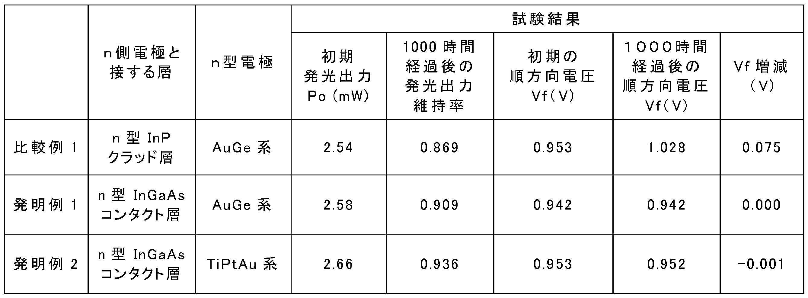
以上の結果から、比較例1では、n型InPクラッド層31をn側電極93と接する層としたために、発光出力Poの維持率が低く、さらに、長時間通電により順方向電圧Vfが大きく上昇したことが確認された。これに対して、発明例1では、n型InGaAsコンタクト層20をn側電極93と接する層としたために、1000時間通電後での発光出力Poの維持率の低下を抑制でき、さらにVf上昇を抑制できたことが確認された。また、発明例2は、発明例1とはn型電極の電極材料のみ異なるが、発明例1と同様に、発光出力Poの維持率の低下を抑制でき、さらにVf上昇を抑制できたことが確認された。なお、n型InGaAsコンタクト層20は、半導体発光素子100の発光波長を光吸収するものの、コンタクト層としてn側電極直下にのみ設けているため、発光出力への影響がないことも確認できた。
From the above results, in Comparative Example 1, since the n-type
本発明によれば、発光出力および順方向電圧の経時変化が少なく、信頼性に優れた、中心発光波長を1000~2200nmとする接合型の半導体発光素子およびその製造方法を提供することができる。 According to the present invention, it is possible to provide a junction-type semiconductor light emitting device having a center emission wavelength of 1000 to 2200 nm, which exhibits little change over time in light emission output and forward voltage, and has excellent reliability, and a method for manufacturing the same.
10 n型InP成長用基板
20 n型InGaAsコンタクト層
30 半導体積層体
31 n型クラッド層
35 活性層
35W 井戸層
35B 障壁層
37 p型クラッド層
39 p型キャップ層
40 中間層
41(41a) p型コンタクト層
43 オーミック金属部
45 p型コンタクト部
47 誘電体層
60 金属層
60A 金属反射層
60B 金属接合層
80 導電性支持基板
100 半導体発光素子
91 裏面電極
93 n側電極
E1 露出領域
E2 露出面
E3 露出部
10 n-type InP growth substrate 20 n-type
Claims (6)
該導電性支持基板上に設けられた、反射金属を含む金属層と、
該金属層上に設けられた、InおよびPを少なくとも含むInGaAsP系III-V族化合物半導体層を複数層積層してなる半導体積層体と、
前記半導体積層体上の一部領域に設けられたn型InGaAsコンタクト層と、
該n型InGaAsコンタクト層上に設けられたn側電極と、を有し、
前記半導体積層体から放出される光の中心発光波長が1000~2200nmであり、
前記n型InGaAsコンタクト層のIn組成比が0.54以上0.60以下であり、
前記半導体積層体の全体の厚みが2μm~8μmであることを特徴とする半導体発光素子。 a conductive support substrate;
a metal layer containing a reflective metal provided on the conductive support substrate;
A semiconductor laminate formed by stacking a plurality of InGaAsP-based III-V compound semiconductor layers containing at least In and P, provided on the metal layer;
an n-type InGaAs contact layer provided in a partial region on the semiconductor stack;
an n-side electrode provided on the n-type InGaAs contact layer;
The center emission wavelength of the light emitted from the semiconductor stack is 1000 to 2200 nm,
The n-type InGaAs contact layer has an In composition ratio of 0.54 or more and 0.60 or less,
A semiconductor light emitting device characterized in that the total thickness of the semiconductor laminate is 2 μm to 8 μm.
前記n型InGaAsコンタクト層上にInおよびPを少なくとも含むInGaAsP系III-V族化合物半導体層を複数層積層した半導体積層体を形成する第2工程と、
前記半導体積層体上に、金属反射層を形成する第3工程と、
金属接合層が表面に設けられた導電性支持基板を、該金属接合層を介して前記金属反射層に接合する第4工程と、
前記n型InP成長用基板を除去する第5工程と、
前記n型InGaAsコンタクト層の前記n側電極形成領域上にn側電極を形成しつつ、前記n型InGaAsコンタクト層を一部除去して、前記半導体積層体に露出面を設ける第6工程と、を有し、
前記半導体積層体から放出される光の中心発光波長が1000~2200nmであり、
前記第1工程において形成する前記n型InGaAsコンタクト層のIn組成比を、0.54以上0.60以下とし、
前記半導体積層体の全体の厚みを2μm~8μmとすることを特徴とする半導体発光素子の製造方法。 A first step of forming an n-type InGaAs contact layer including an n-side electrode formation region on the n-type InP growth substrate;
a second step of forming a semiconductor stack in which a plurality of InGaAsP group III-V compound semiconductor layers containing at least In and P are stacked on the n-type InGaAs contact layer;
a third step of forming a metal reflective layer on the semiconductor stack;
a fourth step of bonding a conductive support substrate provided with a metal bonding layer on the surface to the metal reflective layer via the metal bonding layer;
a fifth step of removing the n-type InP growth substrate;
a sixth step of forming an n-side electrode on the n-side electrode formation region of the n-type InGaAs contact layer and removing a portion of the n-type InGaAs contact layer to provide an exposed surface on the semiconductor stack; has
The center emission wavelength of the light emitted from the semiconductor stack is 1000 to 2200 nm,
The In composition ratio of the n-type InGaAs contact layer formed in the first step is 0.54 or more and 0.60 or less,
A method for manufacturing a semiconductor light emitting device, characterized in that the total thickness of the semiconductor laminate is 2 μm to 8 μm.
Priority Applications (1)
| Application Number | Priority Date | Filing Date | Title |
|---|---|---|---|
| JP2022190567A JP7402962B2 (en) | 2017-12-22 | 2022-11-29 | Semiconductor light emitting device and its manufacturing method |
Applications Claiming Priority (2)
| Application Number | Priority Date | Filing Date | Title |
|---|---|---|---|
| JP2017246594A JP2019114650A (en) | 2017-12-22 | 2017-12-22 | Semiconductor light emitting device and method of manufacturing the same |
| JP2022190567A JP7402962B2 (en) | 2017-12-22 | 2022-11-29 | Semiconductor light emitting device and its manufacturing method |
Related Parent Applications (1)
| Application Number | Title | Priority Date | Filing Date |
|---|---|---|---|
| JP2017246594A Division JP2019114650A (en) | 2017-12-22 | 2017-12-22 | Semiconductor light emitting device and method of manufacturing the same |
Publications (2)
| Publication Number | Publication Date |
|---|---|
| JP2023014201A JP2023014201A (en) | 2023-01-26 |
| JP7402962B2 true JP7402962B2 (en) | 2023-12-21 |
Family
ID=66992640
Family Applications (2)
| Application Number | Title | Priority Date | Filing Date |
|---|---|---|---|
| JP2017246594A Pending JP2019114650A (en) | 2017-12-22 | 2017-12-22 | Semiconductor light emitting device and method of manufacturing the same |
| JP2022190567A Active JP7402962B2 (en) | 2017-12-22 | 2022-11-29 | Semiconductor light emitting device and its manufacturing method |
Family Applications Before (1)
| Application Number | Title | Priority Date | Filing Date |
|---|---|---|---|
| JP2017246594A Pending JP2019114650A (en) | 2017-12-22 | 2017-12-22 | Semiconductor light emitting device and method of manufacturing the same |
Country Status (7)
| Country | Link |
|---|---|
| US (2) | US11508875B2 (en) |
| JP (2) | JP2019114650A (en) |
| KR (1) | KR102441461B1 (en) |
| CN (1) | CN111492494B (en) |
| DE (1) | DE112018006528T5 (en) |
| TW (1) | TWI713235B (en) |
| WO (1) | WO2019124497A1 (en) |
Families Citing this family (8)
| Publication number | Priority date | Publication date | Assignee | Title |
|---|---|---|---|---|
| JP6785331B2 (en) * | 2018-03-30 | 2020-11-18 | Dowaエレクトロニクス株式会社 | Manufacturing method of semiconductor optical device and intermediate of semiconductor optical device |
| WO2019203329A1 (en) | 2018-04-19 | 2019-10-24 | Dowaエレクトロニクス株式会社 | Semiconductor light-emitting element and method for manufacturing same |
| US11515448B2 (en) * | 2018-04-19 | 2022-11-29 | Dowa Electronics Materials Co., Ltd. | Semiconductor light-emitting element and method of manufacturing the same |
| JP2021090004A (en) * | 2019-12-05 | 2021-06-10 | ウシオ電機株式会社 | Infrared LED element |
| JP7716037B2 (en) * | 2020-09-16 | 2025-07-31 | ウシオ電機株式会社 | Infrared LED element |
| WO2023037629A1 (en) * | 2021-09-13 | 2023-03-16 | ウシオ電機株式会社 | Infrared led element |
| TWI859532B (en) * | 2022-04-26 | 2024-10-21 | 晶元光電股份有限公司 | Semiconductor device |
| TW202510039A (en) * | 2023-08-16 | 2025-03-01 | 台亞半導體股份有限公司 | Light emitting diode |
Citations (7)
| Publication number | Priority date | Publication date | Assignee | Title |
|---|---|---|---|---|
| JP2004200375A (en) | 2002-12-18 | 2004-07-15 | Matsushita Electric Ind Co Ltd | Semiconductor laser device and method of manufacturing the same |
| US20070012937A1 (en) | 2005-07-12 | 2007-01-18 | Jin-Hsiang Liu | High-brightness light emitting diode having reflective layer |
| JP2007227895A (en) | 2006-02-23 | 2007-09-06 | Arima Optoelectronics Corp | Light emitting diode by metal diffusion bonding and its manufacturing method |
| JP2008172210A (en) | 2006-12-11 | 2008-07-24 | Nec Electronics Corp | Embedded semiconductor laser and method for manufacturing the same |
| US20100329297A1 (en) | 2009-06-30 | 2010-12-30 | Joseph John Rumpler | Highly integrable edge emitting active optical device and a process for manufacture of the same |
| JP2011165800A (en) | 2010-02-08 | 2011-08-25 | Showa Denko Kk | Light emitting diode, method of manufacturing the same, and light emitting diode lamp |
| JP2013251341A (en) | 2012-05-30 | 2013-12-12 | Sumitomo Electric Ind Ltd | Light receiving element, semiconductor epitaxial wafer, detection device, and method for manufacturing light receiving element |
Family Cites Families (28)
| Publication number | Priority date | Publication date | Assignee | Title |
|---|---|---|---|---|
| US3318519A (en) | 1967-05-09 | Apparatus for transferring values between the | ||
| JPS5871669A (en) | 1981-10-23 | 1983-04-28 | Nec Corp | Both surfaces light emission type light emitting diode |
| JPS6386581A (en) * | 1986-09-30 | 1988-04-16 | Shimadzu Corp | light emitting diode |
| JPH023293A (en) | 1988-06-20 | 1990-01-08 | Toshiba Corp | Manufacture of semiconductor element |
| JPH04249384A (en) * | 1991-02-05 | 1992-09-04 | Nec Corp | Manufacture of semiconductor light emitting element |
| JPH05190970A (en) * | 1992-01-09 | 1993-07-30 | Toshiba Corp | Semiconductor laser manufacturing method |
| JPH0685239A (en) * | 1992-09-01 | 1994-03-25 | Fujitsu Ltd | Manufacture of semiconductor device |
| JP3107660B2 (en) | 1992-09-29 | 2000-11-13 | 株式会社東芝 | Semiconductor light emitting device |
| JPH07111339A (en) * | 1993-10-12 | 1995-04-25 | Sumitomo Electric Ind Ltd | Surface emitting semiconductor light emitting device |
| JPH09181398A (en) * | 1995-12-25 | 1997-07-11 | Sony Corp | Semiconductor light emitting device |
| KR19990035944A (en) * | 1996-05-30 | 1999-05-25 | 사토 게니치로 | Semiconductor light emitting device and manufacturing method thereof |
| JP3898786B2 (en) * | 1996-10-11 | 2007-03-28 | 三菱電機株式会社 | Semiconductor device |
| JP2000068597A (en) * | 1998-08-20 | 2000-03-03 | Hitachi Ltd | Semiconductor device |
| DE10051465A1 (en) * | 2000-10-17 | 2002-05-02 | Osram Opto Semiconductors Gmbh | Method for producing a GaN-based semiconductor component |
| US6878562B2 (en) * | 2000-10-20 | 2005-04-12 | Phosistor Technologies, Incorporated | Method for shifting the bandgap energy of a quantum well layer |
| US8871547B2 (en) * | 2005-01-11 | 2014-10-28 | SemiLEDs Optoelectronics Co., Ltd. | Method for fabricating vertical light emitting diode (VLED) structure using a laser pulse to remove a carrier substrate |
| US8318519B2 (en) * | 2005-01-11 | 2012-11-27 | SemiLEDs Optoelectronics Co., Ltd. | Method for handling a semiconductor wafer assembly |
| JP4835376B2 (en) * | 2006-10-20 | 2011-12-14 | 日立電線株式会社 | Semiconductor light emitting device |
| US8110425B2 (en) * | 2007-03-20 | 2012-02-07 | Luminus Devices, Inc. | Laser liftoff structure and related methods |
| JP2008283096A (en) * | 2007-05-14 | 2008-11-20 | Hitachi Cable Ltd | Semiconductor light emitting device |
| JP5211887B2 (en) | 2007-07-03 | 2013-06-12 | 日亜化学工業株式会社 | Semiconductor light emitting device and manufacturing method thereof |
| KR101221281B1 (en) * | 2008-03-13 | 2013-01-11 | 쇼와 덴코 가부시키가이샤 | Semiconductor light-emitting device and method for manufacturing the same |
| TW201234660A (en) | 2011-02-10 | 2012-08-16 | Dongguan Lei Chau Electronics Co Ltd | Light emitting diode structure and luminosity controlling method thereof |
| GB2504977B (en) * | 2012-08-16 | 2017-10-04 | Airbus Defence & Space Gmbh | Laser power converter |
| KR102098937B1 (en) * | 2014-01-27 | 2020-04-08 | 엘지이노텍 주식회사 | Light emitting device |
| JP6452651B2 (en) * | 2016-06-30 | 2019-01-16 | Dowaエレクトロニクス株式会社 | Semiconductor optical device manufacturing method and semiconductor optical device |
| JP6608352B2 (en) * | 2016-12-20 | 2019-11-20 | Dowaエレクトロニクス株式会社 | Semiconductor light emitting device and manufacturing method thereof |
| US10840408B1 (en) * | 2019-05-28 | 2020-11-17 | Vuereal Inc. | Enhanced efficiency of LED structure with n-doped quantum barriers |
-
2017
- 2017-12-22 JP JP2017246594A patent/JP2019114650A/en active Pending
-
2018
- 2018-12-20 CN CN201880082056.2A patent/CN111492494B/en active Active
- 2018-12-20 US US16/955,043 patent/US11508875B2/en active Active
- 2018-12-20 WO PCT/JP2018/047001 patent/WO2019124497A1/en not_active Ceased
- 2018-12-20 DE DE112018006528.6T patent/DE112018006528T5/en active Pending
- 2018-12-20 KR KR1020207015065A patent/KR102441461B1/en active Active
- 2018-12-21 TW TW107146568A patent/TWI713235B/en active
-
2022
- 2022-11-08 US US18/053,374 patent/US11996496B2/en active Active
- 2022-11-29 JP JP2022190567A patent/JP7402962B2/en active Active
Patent Citations (7)
| Publication number | Priority date | Publication date | Assignee | Title |
|---|---|---|---|---|
| JP2004200375A (en) | 2002-12-18 | 2004-07-15 | Matsushita Electric Ind Co Ltd | Semiconductor laser device and method of manufacturing the same |
| US20070012937A1 (en) | 2005-07-12 | 2007-01-18 | Jin-Hsiang Liu | High-brightness light emitting diode having reflective layer |
| JP2007227895A (en) | 2006-02-23 | 2007-09-06 | Arima Optoelectronics Corp | Light emitting diode by metal diffusion bonding and its manufacturing method |
| JP2008172210A (en) | 2006-12-11 | 2008-07-24 | Nec Electronics Corp | Embedded semiconductor laser and method for manufacturing the same |
| US20100329297A1 (en) | 2009-06-30 | 2010-12-30 | Joseph John Rumpler | Highly integrable edge emitting active optical device and a process for manufacture of the same |
| JP2011165800A (en) | 2010-02-08 | 2011-08-25 | Showa Denko Kk | Light emitting diode, method of manufacturing the same, and light emitting diode lamp |
| JP2013251341A (en) | 2012-05-30 | 2013-12-12 | Sumitomo Electric Ind Ltd | Light receiving element, semiconductor epitaxial wafer, detection device, and method for manufacturing light receiving element |
Also Published As
| Publication number | Publication date |
|---|---|
| US11996496B2 (en) | 2024-05-28 |
| WO2019124497A1 (en) | 2019-06-27 |
| JP2023014201A (en) | 2023-01-26 |
| KR102441461B1 (en) | 2022-09-07 |
| TW201929263A (en) | 2019-07-16 |
| KR20200070381A (en) | 2020-06-17 |
| DE112018006528T5 (en) | 2020-09-03 |
| US20230079138A1 (en) | 2023-03-16 |
| CN111492494A (en) | 2020-08-04 |
| US11508875B2 (en) | 2022-11-22 |
| CN111492494B (en) | 2023-08-01 |
| TWI713235B (en) | 2020-12-11 |
| JP2019114650A (en) | 2019-07-11 |
| US20200381589A1 (en) | 2020-12-03 |
Similar Documents
| Publication | Publication Date | Title |
|---|---|---|
| JP7402962B2 (en) | Semiconductor light emitting device and its manufacturing method | |
| US11417793B2 (en) | Method of manufacturing semiconductor optical device and semiconductor optical device | |
| JP6785331B2 (en) | Manufacturing method of semiconductor optical device and intermediate of semiconductor optical device | |
| KR20190089915A (en) | Semiconductor light emitting device and manufacturing method thereof | |
| JP2021129119A (en) | Manufacturing method of semiconductor optical device, and semiconductor optical device | |
| CN114616684B (en) | Light emitting element and method for manufacturing the same | |
| TWI743463B (en) | Manufacturing method of semiconductor optical element and intermediate of semiconductor optical element | |
| WO2019216308A1 (en) | Semiconductor light-emitting element and method for manufacturing semiconductor light-emitting element | |
| JP6875076B2 (en) | Manufacturing method of semiconductor light emitting device and semiconductor light emitting device |
Legal Events
| Date | Code | Title | Description |
|---|---|---|---|
| A621 | Written request for application examination |
Free format text: JAPANESE INTERMEDIATE CODE: A621 Effective date: 20221129 |
|
| A977 | Report on retrieval |
Free format text: JAPANESE INTERMEDIATE CODE: A971007 Effective date: 20230726 |
|
| A131 | Notification of reasons for refusal |
Free format text: JAPANESE INTERMEDIATE CODE: A131 Effective date: 20230801 |
|
| TRDD | Decision of grant or rejection written | ||
| A01 | Written decision to grant a patent or to grant a registration (utility model) |
Free format text: JAPANESE INTERMEDIATE CODE: A01 Effective date: 20231205 |
|
| A61 | First payment of annual fees (during grant procedure) |
Free format text: JAPANESE INTERMEDIATE CODE: A61 Effective date: 20231211 |
|
| R150 | Certificate of patent or registration of utility model |
Ref document number: 7402962 Country of ref document: JP Free format text: JAPANESE INTERMEDIATE CODE: R150 |