JP7367055B2 - DRAM memory device with Xtacking architecture - Google Patents
DRAM memory device with Xtacking architecture Download PDFInfo
- Publication number
- JP7367055B2 JP7367055B2 JP2021559590A JP2021559590A JP7367055B2 JP 7367055 B2 JP7367055 B2 JP 7367055B2 JP 2021559590 A JP2021559590 A JP 2021559590A JP 2021559590 A JP2021559590 A JP 2021559590A JP 7367055 B2 JP7367055 B2 JP 7367055B2
- Authority
- JP
- Japan
- Prior art keywords
- contact
- substrate
- coupled
- dielectric stack
- array
- Prior art date
- Legal status (The legal status is an assumption and is not a legal conclusion. Google has not performed a legal analysis and makes no representation as to the accuracy of the status listed.)
- Active
Links
Images


Classifications
-
- H—ELECTRICITY
- H10—SEMICONDUCTOR DEVICES; ELECTRIC SOLID-STATE DEVICES NOT OTHERWISE PROVIDED FOR
- H10B—ELECTRONIC MEMORY DEVICES
- H10B12/00—Dynamic random access memory [DRAM] devices
- H10B12/30—DRAM devices comprising one-transistor - one-capacitor [1T-1C] memory cells
-
- H—ELECTRICITY
- H10—SEMICONDUCTOR DEVICES; ELECTRIC SOLID-STATE DEVICES NOT OTHERWISE PROVIDED FOR
- H10B—ELECTRONIC MEMORY DEVICES
- H10B12/00—Dynamic random access memory [DRAM] devices
- H10B12/01—Manufacture or treatment
- H10B12/02—Manufacture or treatment for one transistor one-capacitor [1T-1C] memory cells
- H10B12/03—Making the capacitor or connections thereto
- H10B12/033—Making the capacitor or connections thereto the capacitor extending over the transistor
- H10B12/0335—Making a connection between the transistor and the capacitor, e.g. plug
-
- H—ELECTRICITY
- H10—SEMICONDUCTOR DEVICES; ELECTRIC SOLID-STATE DEVICES NOT OTHERWISE PROVIDED FOR
- H10B—ELECTRONIC MEMORY DEVICES
- H10B12/00—Dynamic random access memory [DRAM] devices
- H10B12/01—Manufacture or treatment
- H10B12/09—Manufacture or treatment with simultaneous manufacture of the peripheral circuit region and memory cells
-
- H10W90/00—
-
- H—ELECTRICITY
- H10—SEMICONDUCTOR DEVICES; ELECTRIC SOLID-STATE DEVICES NOT OTHERWISE PROVIDED FOR
- H10B—ELECTRONIC MEMORY DEVICES
- H10B12/00—Dynamic random access memory [DRAM] devices
- H10B12/01—Manufacture or treatment
- H10B12/02—Manufacture or treatment for one transistor one-capacitor [1T-1C] memory cells
- H10B12/03—Making the capacitor or connections thereto
-
- H—ELECTRICITY
- H10—SEMICONDUCTOR DEVICES; ELECTRIC SOLID-STATE DEVICES NOT OTHERWISE PROVIDED FOR
- H10B—ELECTRONIC MEMORY DEVICES
- H10B12/00—Dynamic random access memory [DRAM] devices
- H10B12/30—DRAM devices comprising one-transistor - one-capacitor [1T-1C] memory cells
- H10B12/31—DRAM devices comprising one-transistor - one-capacitor [1T-1C] memory cells having a storage electrode stacked over the transistor
- H10B12/315—DRAM devices comprising one-transistor - one-capacitor [1T-1C] memory cells having a storage electrode stacked over the transistor with the capacitor higher than a bit line
-
- H—ELECTRICITY
- H10—SEMICONDUCTOR DEVICES; ELECTRIC SOLID-STATE DEVICES NOT OTHERWISE PROVIDED FOR
- H10B—ELECTRONIC MEMORY DEVICES
- H10B12/00—Dynamic random access memory [DRAM] devices
- H10B12/30—DRAM devices comprising one-transistor - one-capacitor [1T-1C] memory cells
- H10B12/48—Data lines or contacts therefor
-
- H—ELECTRICITY
- H10—SEMICONDUCTOR DEVICES; ELECTRIC SOLID-STATE DEVICES NOT OTHERWISE PROVIDED FOR
- H10B—ELECTRONIC MEMORY DEVICES
- H10B12/00—Dynamic random access memory [DRAM] devices
- H10B12/50—Peripheral circuit region structures
-
- H—ELECTRICITY
- H10—SEMICONDUCTOR DEVICES; ELECTRIC SOLID-STATE DEVICES NOT OTHERWISE PROVIDED FOR
- H10D—INORGANIC ELECTRIC SEMICONDUCTOR DEVICES
- H10D1/00—Resistors, capacitors or inductors
- H10D1/60—Capacitors
- H10D1/68—Capacitors having no potential barriers
- H10D1/692—Electrodes
- H10D1/711—Electrodes having non-planar surfaces, e.g. formed by texturisation
-
- H10P10/128—
-
- H10W80/00—
-
- H10W72/019—
-
- H10W72/0198—
-
- H10W72/07236—
-
- H10W72/90—
-
- H10W72/941—
-
- H10W72/951—
-
- H10W80/102—
-
- H10W80/312—
-
- H10W80/327—
-
- H10W80/701—
-
- H10W90/792—
-
- H10W99/00—
Landscapes
- Engineering & Computer Science (AREA)
- Manufacturing & Machinery (AREA)
- Microelectronics & Electronic Packaging (AREA)
- Power Engineering (AREA)
- Computer Hardware Design (AREA)
- Semiconductor Memories (AREA)
- Physics & Mathematics (AREA)
- Condensed Matter Physics & Semiconductors (AREA)
- General Physics & Mathematics (AREA)
Description
ダイナミックランダムアクセスメモリ(RAM)は、キャパシタとアレイトランジスタとを有するメモリセル内にデータの各ビットを記憶するランダムアクセスメモリの一種であり、キャパシタとアレイトランジスタは両方とも典型的には金属酸化膜半導体(MOS)技術に基づく。キャパシタは、充電状態または放電状態のいずれかに設定することができる。これらの2つの状態は、従来0および1と呼ばれているビットの2つの値を表すためにとられる。DRAMは、周辺回路を形成するために周辺トランジスタも含む。周辺回路およびアレイトランジスタは、データ入力/出力(I/O)ならびにメモリセル動作(例えば、書き込みまたは読み取り)を処理する。 Dynamic random access memory (RAM) is a type of random access memory that stores each bit of data in a memory cell that has a capacitor and an array transistor, both of which are typically metal oxide semiconductors. (MOS) technology. A capacitor can be set to either a charging state or a discharging state. These two states are taken to represent two values of the bits, conventionally referred to as 0 and 1. DRAMs also include peripheral transistors to form peripheral circuitry. Peripheral circuits and array transistors handle data input/output (I/O) and memory cell operations (eg, writes or reads).
DRAM技術がより高密度およびより大容量に、例えば、10nmノードに向かうにつれて、キャパシタの数は劇的に増加し、キャパシタのサイズは劇的に減少する。キャパシタの数およびサイズの変化は、より長いプロセス時間と、より複雑なプロセスフローとをもたらす可能性がある。 As DRAM technology moves toward higher densities and larger capacities, eg, the 10 nm node, the number of capacitors increases dramatically and the size of the capacitors decreases dramatically. Varying the number and size of capacitors can result in longer process times and more complex process flows.
本概念は、DRAMメモリデバイス、例えば、Xtackingアーキテクチャを有するDRAMメモリデバイスの形成に関する。Xtackingアーキテクチャでは、DRAMメモリデバイスのキャパシタは、アレイウェハ上で処理され、DRAMメモリデバイスの周辺トランジスタおよびアレイトランジスタは、所望のI/O速度および機能を可能にする論理技術ノードを使用して別の周辺ウェハ上で処理される。アレイウェハおよび周辺ウェハの処理が完了すると、2つのウェハは、1つのプロセスステップにおいてウェハ間の界面を横切って形成される金属ビア(垂直相互接続アクセス)を介して電気的に接続される。Xtacking技術を使用することによって、より高い記憶密度、より単純なプロセスフロー、およびより短いサイクル時間を達成することができる。 The present concepts relate to the formation of DRAM memory devices, eg, DRAM memory devices having an Xtacking architecture. In an Processed on wafer. Once processing of the array and peripheral wafers is complete, the two wafers are electrically connected through metal vias (vertical interconnect access) that are formed across the interface between the wafers in one process step. By using Xtacking technology, higher storage densities, simpler process flows, and shorter cycle times can be achieved.
本開示の一態様によれば、アレイトランジスタが中に形成された第1のウェハと、キャパシタ構造が中に形成された第2のウェハとを含むことができる半導体デバイスが提供される。半導体デバイスは、第1のウェハと第2のウェハとの間に形成された、複数の接合構造を含む接合界面も含む。接合構造は、メモリセルを形成するためにアレイトランジスタをキャパシタ構造に結合するように構成される。 According to one aspect of the present disclosure, a semiconductor device is provided that can include a first wafer with an array transistor formed therein and a second wafer with a capacitor structure formed therein. The semiconductor device also includes a bonding interface formed between the first wafer and the second wafer that includes a plurality of bonding structures. A junction structure is configured to couple the array transistor to the capacitor structure to form a memory cell.
いくつかの実施形態において、第1のウェハは、第1の基板を有することができ、第2のウェハは、第2の基板を有することができる。第1の基板は、第1の面と、反対側の第2の面とを有する。第2の基板は、第1の面と、反対側の第2の面とを有する。アレイトランジスタは、第1の基板の第1の面内に配置することができる。 In some embodiments, a first wafer can have a first substrate and a second wafer can have a second substrate. The first substrate has a first surface and an opposite second surface. The second substrate has a first surface and an opposite second surface. The array transistor may be disposed within the first surface of the first substrate.
加えて、半導体デバイスは、アレイトランジスタ上に形成され、第1の基板の第1の面上に配置された第1の誘電体スタックと、第1の誘電体スタック内に形成され、第1の誘電体スタックを通って延在する複数の第1のコンタクト構造とを含むことができ、第1のコンタクト構造の第1の端子コンタクトは、アレイトランジスタの第1のドープ領域に結合される。半導体デバイスは、キャパシタ構造が第2の誘電体スタック内に配置されるように、第2の基板の第1の面上に形成された第2の誘電体スタックも含むことができ、複数の第2のコンタクト構造が、第2の誘電体スタック内に形成され、第2の誘電体スタックを通ってさらに延在する。半導体デバイスは、第2の基板の第2の面上に形成された第3の誘電体スタックと、第3の誘電体スタック内に形成されたシリコン貫通コンタクト(TSC(through silicon contact))とを含むことができる。TSCは、第2のコンタクト構造の第2の端子コンタクトに接続するように、第2の基板の第2の面から第2の基板を通って延在することができる。 Additionally, the semiconductor device includes a first dielectric stack formed over the array transistor and disposed on the first side of the first substrate; a plurality of first contact structures extending through the dielectric stack, a first terminal contact of the first contact structure being coupled to a first doped region of the array transistor. The semiconductor device can also include a second dielectric stack formed on the first side of the second substrate such that the capacitor structure is disposed within the second dielectric stack, and the semiconductor device includes a plurality of dielectric stacks formed on the first side of the second substrate. Two contact structures are formed within and extend further through the second dielectric stack. The semiconductor device includes a third dielectric stack formed on the second side of the second substrate and a through silicon contact (TSC) formed within the third dielectric stack. can be included. The TSC can extend from a second side of the second substrate through the second substrate to connect to a second terminal contact of the second contact structure.
アレイトランジスタは、ゲート構造と、第2のドープ領域とをさらに含むことができる。ゲート構造は、第1のコンタクト構造のワードライン構造に結合することができ、第2のドープ領域は、第1のコンタクト構造のビットライン構造に結合することができる。 The array transistor can further include a gate structure and a second doped region. The gate structure can be coupled to the word line structure of the first contact structure and the second doped region can be coupled to the bit line structure of the first contact structure.
キャパシタ構造は、カップ状の底板を有することができる。底板は、第2の誘電体スタック内に形成することができる。底板は、第2の基板の第1の面から離れる方へさらに延在し、第2のコンタクト構造の底板コンタクトに結合される。キャパシタ構造は、底板内に配置され、第2のコンタクト構造の上板コンタクトに結合された細長い上板を有することもできる。底板と上板との間に、高K層がさらに配置される。 The capacitor structure can have a cup-shaped bottom plate. A bottom plate can be formed within the second dielectric stack. The bottom plate further extends away from the first side of the second substrate and is coupled to the bottom plate contacts of the second contact structure. The capacitor structure can also have an elongated top plate disposed within the bottom plate and coupled to the top plate contact of the second contact structure. A high-K layer is further disposed between the bottom plate and the top plate.
いくつかの実施形態において、底板コンタクトおよび第1の端子コンタクトは、一緒に接合することができ、ビットライン構造および第2の端子コンタクトは、一緒に接合することができる。 In some embodiments, the bottom plate contact and the first terminal contact can be bonded together, and the bit line structure and the second terminal contact can be bonded together.
半導体デバイスは、第1の基板の第1の面内に形成された周辺トランジスタをさらに含むことができる。周辺トランジスタは、第1のコンタクト構造のゲートコンタクトに接続されたゲート構造と、第1のコンタクト構造のソースコンタクトに接続されたソース領域と、第1のコンタクト構造のドレインコンタクトに接続されたドレイン領域とを有することができる。ゲートコンタクト、ソースコンタクト、およびドレインコンタクトの各々は、それぞれの第2のコンタクト構造に接合することができる。 The semiconductor device can further include a peripheral transistor formed in the first surface of the first substrate. The peripheral transistor includes a gate structure connected to the gate contact of the first contact structure, a source region connected to the source contact of the first contact structure, and a drain region connected to the drain contact of the first contact structure. and can have. Each of the gate contact, source contact, and drain contact can be joined to a respective second contact structure.
別の実施形態において、半導体デバイスは、第2の基板の第1の面内に形成された周辺トランジスタを有することができる。したがって、周辺トランジスタは、第2のコンタクト構造のゲートコンタクトに接続されたゲート構造と、第2のコンタクト構造のソースコンタクトに接続されたソース領域と、第2のコンタクト構造のドレインコンタクトに接続されたドレイン領域とを有する。ゲートコンタクト、ソースコンタクト、およびドレインコンタクトの各々は、それぞれの第1のコンタクト構造に接合される。 In another embodiment, a semiconductor device can have a peripheral transistor formed in the first side of the second substrate. Accordingly, the peripheral transistor has a gate structure connected to the gate contact of the second contact structure, a source region connected to the source contact of the second contact structure, and a drain contact of the second contact structure. and a drain region. Each of the gate contact, source contact, and drain contact is joined to a respective first contact structure.
本開示の別の態様によれば、半導体デバイスを製造するための方法が提供される。開示された方法において、第1の基板の第1の面上のアレイトランジスタを形成することができる。第1の誘電体スタックが、アレイトランジスタ上に形成され、第1の基板の第1の面上に配置され、複数の第1のコンタクト構造が、第1の誘電体スタック内に形成され、アレイトランジスタは、第1のコンタクト構造の少なくとも1つに結合される。加えて、キャパシタ構造を、第2の基板の第1の面上にさらに形成することができる。第2の誘電体スタックが、第2の基板の第1の面上に形成され、複数の第2のコンタクト構造が、第2の誘電体スタック内に形成され、キャパシタ構造は、第2のコンタクト構造の少なくとも1つに結合され、キャパシタ構造は、第2の誘電体スタック内に配置される。第1の基板および第2の基板は、その後、キャパシタ構造がアレイトランジスタに結合され、第1の基板の第1の面と第2の基板の第1の面とが互いに向かい合うように、複数の接合構造を介して互いに接合することができる。 According to another aspect of the disclosure, a method for manufacturing a semiconductor device is provided. In the disclosed method, an array transistor can be formed on a first side of a first substrate. A first dielectric stack is formed over the array transistor and disposed on the first side of the first substrate, a plurality of first contact structures are formed within the first dielectric stack, and the array A transistor is coupled to at least one of the first contact structures. Additionally, a capacitor structure can be further formed on the first side of the second substrate. A second dielectric stack is formed on the first side of the second substrate, a plurality of second contact structures are formed within the second dielectric stack, and a capacitor structure is formed on the second contact. coupled to at least one of the structures, a capacitor structure is disposed within the second dielectric stack. The first substrate and the second substrate then have a plurality of They can be joined to each other via a joining structure.
方法は、第1の基板の第1の面内に周辺トランジスタを形成するステップを含むこともできる。周辺トランジスタは、第1のコンタクト構造のゲートコンタクトに接続されたゲート構造と、第1のコンタクト構造のソースコンタクトに接続されたソース領域と、第1のコンタクト構造のドレインコンタクトに接続されたドレイン領域とを含むことができ、ゲートコンタクト、ソースコンタクト、およびドレインコンタクトの各々は、それぞれの第2のコンタクト構造に接合される。 The method can also include forming a peripheral transistor in the first side of the first substrate. The peripheral transistor includes a gate structure connected to the gate contact of the first contact structure, a source region connected to the source contact of the first contact structure, and a drain region connected to the drain contact of the first contact structure. and a gate contact, a source contact, and a drain contact each bonded to a respective second contact structure.
いくつかの実施形態において、アレイトランジスタを形成するステップは、ゲート構造と、第1のドープ領域と、第2のドープ領域とを形成するステップを含むことができる。ゲート構造は、第1のコンタクト構造のワードライン構造に結合することができ、第1のドープ領域は、第1のコンタクト構造の第1の端子コンタクトに結合することができ、第2のドープ領域は、第1のコンタクト構造のビットライン構造に結合することができる。 In some embodiments, forming an array transistor can include forming a gate structure, a first doped region, and a second doped region. The gate structure can be coupled to the word line structure of the first contact structure, the first doped region can be coupled to the first terminal contact of the first contact structure, and the first doped region can be coupled to the first terminal contact of the first contact structure; can be coupled to the bit line structure of the first contact structure.
いくつかの実施形態において、第2の基板の一部は、第2の基板の第1の面とは反対側の第2の面から除去することができる。続いて、第3の誘電体スタックを、第2の基板の第2の面上に形成することができる。シリコン貫通コンタクト(TSC)を、第3の誘電体スタック内に形成することができる。TSCは、第2の基板の第2の面から延在し、第2のコンタクト構造の第2の端子コンタクトに接続するように第2の基板を通ってさらに延在することができる。 In some embodiments, a portion of the second substrate can be removed from a second side of the second substrate opposite the first side. A third dielectric stack can then be formed on the second side of the second substrate. A through silicon contact (TSC) may be formed within the third dielectric stack. The TSC may extend from the second side of the second substrate and further extend through the second substrate to connect to a second terminal contact of the second contact structure.
キャパシタ構造を形成するために、カップ状の底板を形成することができる。底板は、第2の誘電体スタック内に配置され、第2のコンタクト構造の底板コンタクトに接続するように第2の基板の第1の面から離れる方へ延在することができる。さらに、細長い上板を形成することができる。上板は、底板内に配置され、第2のコンタクト構造の上板コンタクトに結合することができる。底板と上板との間に、高K層を配置することができる。 A cup-shaped bottom plate can be formed to form a capacitor structure. A bottom plate is disposed within the second dielectric stack and can extend away from the first side of the second substrate to connect to the bottom plate contacts of the second contact structure. Furthermore, an elongated top plate can be formed. A top plate can be disposed within the bottom plate and coupled to the top plate contacts of the second contact structure. A high-K layer can be disposed between the bottom plate and the top plate.
いくつかの実施形態において、第1の基板と第2の基板とを接合するステップは、キャパシタ構造がアレイトランジスタの第1のドープ領域に結合されるように、底板コンタクトと第1の端子コンタクトとを一緒に接合するステップと、TSCがアレイトランジスタの第2のドープ領域に結合されるように、ビットライン構造と第2の端子コンタクトとを一緒に接合するステップとを含むことができる。 In some embodiments, bonding the first substrate and the second substrate includes bonding the bottom plate contact and the first terminal contact such that the capacitor structure is coupled to the first doped region of the array transistor. and bonding together the bit line structure and the second terminal contact such that the TSC is coupled to the second doped region of the array transistor.
開示された方法において、第2の基板の第1の面内に、周辺トランジスタも形成することができる。周辺トランジスタは、第2のコンタクト構造のゲートコンタクトに結合されたゲート構造と、第2のコンタクト構造のソースコンタクトに接続されたソース領域と、第2のコンタクト構造のドレインコンタクトに接続されたドレイン領域とを有することができる。ゲートコンタクト、ソースコンタクト、およびドレインコンタクトの各々は、それぞれの第1のコンタクト構造にさらに接合される。 Peripheral transistors may also be formed in the first side of the second substrate in the disclosed method. The peripheral transistor includes a gate structure coupled to the gate contact of the second contact structure, a source region coupled to the source contact of the second contact structure, and a drain region coupled to the drain contact of the second contact structure. and can have. Each of the gate contact, source contact, and drain contact is further joined to the respective first contact structure.
本開示のさらに別の態様によれば、半導体デバイスが提供される。半導体デバイスは、第1の基板の第1の面上に形成された第1のアレイ領域と第1の周辺領域とを有することができる。第1のアレイ領域は、第1の基板の第1の面内に形成された少なくとも1つのアレイトランジスタを有し、第1の周辺領域は、第1の基板の第1の面内に形成された少なくとも1つの周辺トランジスタを有する。半導体デバイスは、第2の基板の第1の面上に形成された第2のアレイ領域と第2の周辺領域とを有することができる。第2のアレイ領域は、第2の基板の第1の面上に形成された少なくとも1つのキャパシタ構造を有し、少なくとも1つのキャパシタ構造は、少なくとも1つのアレイトランジスタの第1のドープ領域に結合することができる。第1の基板の第1の面と第2の基板の第1の面とは、互いに向かい合う。半導体デバイスは、第1のアレイ領域を第2のアレイ領域に接合し、第1の周辺領域を第2の周辺領域に接合するように構成された複数の接合構造を有することもできる。 According to yet another aspect of the disclosure, a semiconductor device is provided. A semiconductor device can have a first array region and a first peripheral region formed on a first side of a first substrate. The first array region has at least one array transistor formed in the first surface of the first substrate, and the first peripheral region has at least one array transistor formed in the first surface of the first substrate. and at least one peripheral transistor. The semiconductor device can have a second array region and a second peripheral region formed on the first side of the second substrate. The second array region has at least one capacitor structure formed on the first side of the second substrate, the at least one capacitor structure coupled to the first doped region of the at least one array transistor. can do. The first surface of the first substrate and the first surface of the second substrate face each other. The semiconductor device can also have a plurality of bonding structures configured to bond a first array region to a second array region and bond a first peripheral region to a second peripheral region.
半導体デバイスは、第1の基板の第1の面上の少なくとも1つのアレイトランジスタ上に形成された第1の誘電体スタックと、第1の誘電体スタック内に形成され、第1の誘電体スタックを通って延在する複数の第1のコンタクト構造とを有することができ、第1のコンタクト構造の第1の端子コンタクトが、少なくとも1つのアレイトランジスタの第1のドープ領域に結合される。半導体デバイスは、少なくとも1つのキャパシタ構造が第2の誘電体スタック内に配置されるように第2の基板の第1の面上に形成された第2の誘電体スタックと、第2の誘電体スタック内に形成され、第2の誘電体スタックを通って延在する複数の第2のコンタクト構造とを有することもできる。半導体デバイスは、第2の基板の第2の面上に形成された第3の誘電体スタックと、第3の誘電体スタック内に形成された少なくとも1つのシリコン貫通コンタクト(TSC)とをさらに有することができる。第2の基板の第2の面は、第2の基板の第1の面の反対側である。TSCは、第2のコンタクト構造の第2の端子コンタクトに接続するように、第2の基板の第2の面から第2の基板を通って延在することができる。 A semiconductor device includes: a first dielectric stack formed over at least one array transistor on a first side of a first substrate; and a first dielectric stack formed within the first dielectric stack; and a first terminal contact of the first contact structure is coupled to a first doped region of the at least one array transistor. The semiconductor device includes: a second dielectric stack formed on the first side of the second substrate such that at least one capacitor structure is disposed within the second dielectric stack; and a plurality of second contact structures formed within the stack and extending through the second dielectric stack. The semiconductor device further includes a third dielectric stack formed on the second side of the second substrate and at least one through-silicon contact (TSC) formed within the third dielectric stack. be able to. The second surface of the second substrate is opposite the first surface of the second substrate. The TSC can extend from a second side of the second substrate through the second substrate to connect to a second terminal contact of the second contact structure.
いくつかの実施形態において、少なくとも1つのアレイトランジスタは、第1のコンタクト構造のワードライン構造に結合されたゲート構造と、第1のコンタクト構造のビットライン構造に結合された第2のドープ領域とをさらに含むことができる。いくつかの実施形態において、少なくとも1つのキャパシタ構造は、カップ状底板と、細長い上板と、高K層とをさらに含むことができる。底板は、第2の誘電体スタック内に形成され、第2の基板の第1の面から離れる方へ延在し、第2のコンタクト構造の底板コンタクトに結合される。細長い上板は、底板内に配置され、第2のコンタクト構造の上板コンタクトに結合される。高K層は、底板と上板との間に配置される。底板コンタクトおよび第1の端子コンタクトは、一緒に接合され、ビットライン構造および第2の端子コンタクトは、一緒に接合される。 In some embodiments, the at least one array transistor includes a gate structure coupled to a wordline structure of the first contact structure and a second doped region coupled to a bitline structure of the first contact structure. may further include. In some embodiments, the at least one capacitor structure can further include a cup-shaped bottom plate, an elongated top plate, and a high-K layer. A bottom plate is formed within the second dielectric stack, extends away from the first side of the second substrate, and is coupled to the bottom plate contacts of the second contact structure. An elongated top plate is disposed within the bottom plate and coupled to the top plate contact of the second contact structure. A high-K layer is disposed between the bottom plate and the top plate. The bottom plate contact and the first terminal contact are bonded together, and the bit line structure and the second terminal contact are bonded together.
本開示の態様は、添付の図とともに読まれたときに以下の詳細な説明から最もよく理解される。業界における標準的な慣行に従い、様々な特徴が縮尺通りに描かれていないことに留意されたい。実際には、様々な特徴の寸法は、議論を明確にするために増加または減少される場合がある。 Aspects of the present disclosure are best understood from the following detailed description when read in conjunction with the accompanying figures. Note that, following standard industry practice, the various features are not drawn to scale. In practice, the dimensions of various features may be increased or decreased for clarity of discussion.
以下の開示は、提供された主題の異なる特徴を実装するための多くの異なる実施形態または例を提供する。本開示を簡略化するために、構成要素および配置の特定の例について以下に説明する。もちろん、これらは、単なる例であり、限定することを意図していない。例えば、以下の説明における第2の特徴の上の第1の特徴の形成は、第1および第2の特徴が直接接触し得る特徴である実施形態を含み得、また、第1および第2の特徴が直接接触しない場合があるように、第1の特徴と第2の特徴との間に追加の特徴が形成され得る実施形態も含み得る。加えて、本開示は、様々な例において参照番号および/または文字を繰り返す場合がある。この繰り返しは、単純化および明確化の目的のためのものであり、それ自体が、議論されている様々な実施形態および/または構成の間の関係を指示するものではない。 The following disclosure provides many different embodiments or examples for implementing different features of the provided subject matter. To simplify the disclosure, specific examples of components and arrangements are described below. Of course, these are just examples and are not intended to be limiting. For example, the formation of a first feature over a second feature in the following description may include embodiments in which the first and second features are features that can be in direct contact; Embodiments may also be included in which additional features may be formed between the first feature and the second feature, such that the features may not be in direct contact. Additionally, this disclosure may repeat reference numbers and/or characters in various instances. This repetition is for the purpose of simplicity and clarity and does not itself imply a relationship between the various embodiments and/or configurations discussed.
さらに、「の下に」、「より下に」、「下部の」、「より上に」、「上部の」などの空間的に相対的な用語は、本明細書では、図に示されているように、ある要素または特徴の別の要素または特徴との関係を説明するために、説明を容易にするために使用される場合がある。空間的に相対的な用語は、図に示されている向きに加えて、使用中または動作中のデバイスの様々な向きを包含することを意図している。装置は、他の状態に方向付けられ得(90度または他の向きに回転され得)、本明細書で使用される空間的に相対的な記述語も、同様にそれに応じて解釈され得る。 Additionally, spatially relative terms such as "below," "below," "below," "above," and "above" are used herein as indicated in the figures. may be used to facilitate explanation, to describe the relationship of one element or feature to another. Spatially relative terms are intended to encompass various orientations of the device in use or operation in addition to the orientation shown in the figures. The device may be oriented in other positions (rotated 90 degrees or other orientations), and the spatially relative descriptors used herein may be interpreted accordingly.
DRAMメモリデバイスは、アレイ領域と、周辺領域とを含むことができる。アレイ領域は、複数のDRAMメモリセルを含むことができる。DRAMメモリセルの各々は、両方とも典型的には金属酸化膜半導体(MOS)技術に基づくキャパシタおよびアレイトランジスタから形成することができる。キャパシタは、充電または放電することができる。これらの2つの状態は、従来0および1と呼ばれている、ビットの2つの値を表すためにとられる。キャパシタは、製造方法に応じて、フラット構成、スタック構成、またはトレンチ構成において形成することができる。キャパシタは、第1のドープ領域を介して充電または放電されるように、アレイトランジスタの第1のドープ領域(例えば、ドレイン領域)に結合することができる。ワードラインは、アレイトランジスタをオンまたはオフにするために、アレイトランジスタのゲートに結合することができる。ビットラインは、アレイトランジスタの第2のドープ領域(例えば、ソース領域)に結合し、キャパシタを充電または放電するための経路として機能することができる。 A DRAM memory device can include an array region and a peripheral region. The array region can include multiple DRAM memory cells. Each DRAM memory cell may be formed from a capacitor and an array transistor, both typically based on metal oxide semiconductor (MOS) technology. Capacitors can be charged or discharged. These two states are taken to represent two values of the bit, conventionally referred to as 0 and 1. Capacitors can be formed in flat, stacked, or trenched configurations, depending on the manufacturing method. A capacitor can be coupled to a first doped region (eg, a drain region) of the array transistor such that the capacitor is charged or discharged through the first doped region. The word line can be coupled to the gate of the array transistor to turn the array transistor on or off. The bit line can couple to a second doped region (eg, a source region) of the array transistor and serve as a path for charging or discharging the capacitor.
周辺領域は、DRAMメモリセルの書き込みまたは読み取りなど、DRAMメモリセルを動作させるように構成された周辺回路を形成するために、複数の周辺トランジスタを含むことができる。周辺回路は、行デコーダ、列デコーダ、入力/出力コントローラ、マルチプレクサ、センス増幅器などを含むことができる。行デコーダは、DRAMメモリセルのワードラインに結合され、アレイトランジスタのゲートをオンまたはオフにするように構成される。列デコーダは、DRAMメモリセルのビットラインに結合され、DRAMメモリセルの読み取りまたは書き込みを行うように構成される。入力/出力コントローラは、入力信号と出力信号とを制御するように構成される。マルチプレクサは、いくつかの入力信号の中から入力信号を選択し、選択された入力信号を単一の出力ラインに転送するように構成される。センス増幅器は、DRAMメモリセル内に記憶されたデータビット(0または1)を表すビットラインからの低電力信号を感知し、小さい電圧スイングを認識可能な論理レベルに増幅するように構成されるので、データは、DRAMメモリデバイスの外部のロジックによって適切に解釈することができる。 The peripheral region may include a plurality of peripheral transistors to form peripheral circuitry configured to operate the DRAM memory cell, such as writing or reading the DRAM memory cell. Peripheral circuits may include row decoders, column decoders, input/output controllers, multiplexers, sense amplifiers, and the like. The row decoder is coupled to the word line of the DRAM memory cell and is configured to turn on or off the gates of the array transistors. The column decoder is coupled to the bit line of the DRAM memory cell and is configured to read or write to the DRAM memory cell. The input/output controller is configured to control input signals and output signals. A multiplexer is configured to select an input signal among several input signals and forward the selected input signal to a single output line. A sense amplifier is configured to sense low power signals from a bit line representing a data bit (0 or 1) stored within a DRAM memory cell and amplify small voltage swings to a recognizable logic level. , the data can be appropriately interpreted by logic external to the DRAM memory device.
図1Aは、フラット構成において形成されたDRAMメモリセルの概略図であり、キャパシタは、基板(図示せず)の上面上に形成され、上面に沿って延在する。図1Bは、スタック構成において形成されたDRAMメモリデバイスの概略図であり、キャパシタは、基板(図示せず)上に配置された誘電体スタック内に形成される。図1Cは、トレンチ構成において形成されたDRAMメモリデバイスの概略図であり、キャパシタは、基板(図示せず)内に配置される。図1AにおけるDRAMメモリセルと比較すると、図1B~図1CにおけるDRAMメモリセルは、DRAMメモリセルのサイズを縮小し、DRAMメモリデバイスの記憶密度を高めることができる。 FIG. 1A is a schematic diagram of a DRAM memory cell formed in a flat configuration, with a capacitor formed on and extending along the top surface of a substrate (not shown). FIG. 1B is a schematic diagram of a DRAM memory device formed in a stacked configuration, where a capacitor is formed in a dielectric stack disposed on a substrate (not shown). FIG. 1C is a schematic diagram of a DRAM memory device formed in a trench configuration, with a capacitor disposed within a substrate (not shown). Compared to the DRAM memory cell in FIG. 1A, the DRAM memory cell in FIGS. 1B-1C can reduce the size of the DRAM memory cell and increase the storage density of the DRAM memory device.
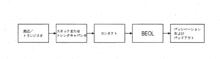
図2は、DRAMメモリデバイスを製造するためのプロセスフローである。図2に示すように、アレイトランジスタ、周辺トランジスタ、およびキャパシタは、同じウェハにおいて順次に処理される。DRAM技術がより高い密度および大容量に向かうにつれて、DRAMメモリデバイスは、より長いプロセス時間と、より複雑なプロセスフロートを必要とする。 FIG. 2 is a process flow for manufacturing a DRAM memory device. As shown in FIG. 2, array transistors, peripheral transistors, and capacitors are processed sequentially on the same wafer. As DRAM technology moves toward higher densities and larger capacities, DRAM memory devices require longer process times and more complex process floats.
図3は、スタック構成において形成されたDRAMメモリデバイス100(デバイス100とも呼ばれる)の断面図であり、キャパシタ、アレイトランジスタ、および周辺トランジスタは、同じウェハ内に形成される。単純化および明確化のために、アレイトランジスタ104、周辺トランジスタ106、およびキャパシタ108が図3に示されている。図3に示すように、アレイトランジスタ104、周辺トランジスタ106、およびキャパシタ108は、同じウェハ102内に形成される。ウェハ102は、基板110を有することができる。基板110は、Si基板などの半導体基板であり得る。アレイトランジスタ104および周辺トランジスタ106は、基板110内に配置される。誘電体スタック101は、基板110上に形成される。誘電体スタック101は、1つまたは複数の誘電体層を含むことができる。図3の例示的な実施形態において、誘電体スタック101は、4つの層間誘電体(ILD(inter layer dielectric))層112~118を含むことができる。キャパシタ108は、誘電体スタック101内に形成される。
FIG. 3 is a cross-sectional view of a DRAM memory device 100 (also referred to as device 100) formed in a stacked configuration, where the capacitor, array transistor, and peripheral transistor are formed within the same wafer.
いくつかの実施形態において、ILD層112~118は、ボロホスホシリケートガラス(BPSG)、ドープされていないシリケートガラス(USG)、ホスホシリケートガラス(PSG)、テトラエチルオルトシリケート(TEOS)、SiH4酸化物、SiO2、スピンオン誘電体(SOD)、または他の適切な誘電体のうちの1つを含むことができる。ILD層112~118は、10nmから10μmの範囲における厚さを有することができる。 In some embodiments, the ILD layers 112-118 are borophosphosilicate glass (BPSG), undoped silicate glass (USG), phosphosilicate glass (PSG), tetraethylorthosilicate (TEOS), SiH 4 oxide , SiO 2 , spin-on dielectric (SOD), or other suitable dielectric. ILD layers 112-118 can have a thickness in the range of 10 nm to 10 μm.
アレイトランジスタ104は、コンタクト構造124を介してキャパシタ108に結合された第1のドープ領域(例えば、ドレイン領域)120を有することができる。アレイトランジスタ104は、第1の接続チャネルを介してビットラインに結合された第2のドープ領域(例えば、ソース領域)122を有することができる。第1の接続チャネルは、コンタクト構造126、ビア128、および第1の金属(M1)層130から形成することができる。アレイトランジスタ104は、第2の接続チャネルを介してワードラインに結合されたゲート132を有することができる。第2の接続チャネルは、コンタクト134、ビア136、およびM1層138から形成することができる。
本開示において、DRAMメモリデバイスは、Xtackingアーキテクチャに基づいて形成される。Xtackingアーキテクチャでは、第1の実施形態において、DRAMメモリデバイスのキャパシタは、アレイウェハ上で処理され、DRAMメモリデバイスの周辺トランジスタおよびアレイトランジスタは、論理技術ノードを使用して別の周辺ウェハ上で処理される。代替実施形態において、DRAMメモリデバイスのキャパシタおよび周辺トランジスタは、周辺ウェハ上で処理することができ、アレイトランジスタは、アレイウェハ上で処理することができる。 In this disclosure, a DRAM memory device is formed based on the Xtacking architecture. In the Xtacking architecture, in a first embodiment, the capacitors of the DRAM memory device are processed on an array wafer, and the peripheral transistors and array transistors of the DRAM memory device are processed on another peripheral wafer using logic technology nodes. Ru. In alternative embodiments, the capacitors and peripheral transistors of the DRAM memory device can be processed on the peripheral wafer, and the array transistors can be processed on the array wafer.
図4Aは、第1の例示的なDRAMメモリデバイス200A(デバイス200Aとも呼ばれる)の断面図であり、図4Bは、第2の例示的なDRAMメモリデバイス200B(デバイス200Bとも呼ばれる)の断面図である。デバイス200Aおよび200Bは、Xtackingアーキテクチャに基づいて形成される。図4Aに示すように、デバイス200Aは、第1のウェハ1内に形成された第1のアレイ領域3および第1の周辺領域4と、第2のウェハ2内に形成された第2のアレイ領域5および第2の周辺領域6とを有することができる。第1のウェハ1は、第1の基板10を有することができ、第2のウェハ2は、第2の基板60を有することができる。第1の基板10は、第1の面10aと、反対側の第2の面10bとを有することができる。第2の基板60は、第1の面60aと、反対側の第2の面60bとを有することができる。
4A is a cross-sectional view of a first exemplary
第1のアレイ領域3および第1の周辺領域4は、第1の基板10の第1の面10a上に形成される。第1のアレイ領域3は、複数のアレイトランジスタを有することができ、第1の周辺領域4は、複数の周辺トランジスタを有することができる。単純化および明確化のために、アレイトランジスタ14および周辺トランジスタ16を図4Aに示す。アレイトランジスタ14および周辺トランジスタ16は、第1の基板10の第1の面10a内に形成することができ、シャロートレンチアイソレーション(STI(shallow trench isolation))34によって互いに離間させることができる。
The
アレイトランジスタ14は、第1の基板10内に形成された、第1のドープ領域(例えば、ドレイン領域)24と、第2のドープ領域(例えば、ソース領域)26とを有することができる。アレイトランジスタ14は、第1の基板10の第1の面10a上に配置されたゲート構造18と、第1の基板10内に配置され、アレイトランジスタ14のボディとして機能するp型ドープウェル(PW)20とを有することができる。ゲート誘電体層22は、ゲート構造18とPW20との間に配置される。誘電体スペーサ21は、ゲート構造18およびゲート誘電体層22の側壁に沿って配置することができる。
周辺トランジスタ16は、回路設計に応じて、n型トランジスタまたはp型トランジスタとすることができる。周辺トランジスタ16は、第1の基板10内に配置された、第1のソース/ドレイン(S/D)領域36と、第2のS/D領域38とを有することができる。周辺トランジスタ16は、第1の基板10上に配置されたゲート構造40と、第1の基板10内に配置され、周辺トランジスタ16のボディとして機能するドープウェル領域44とを有することができる。ゲート誘電体層42は、ゲート構造40とドープウェル領域44との間に配置される。ドープウェル領域44は、周辺トランジスタ16構造に応じて、n型ドーパントまたはp型ドーパントを有することができる。誘電体スペーサ41は、ゲート構造40およびゲート誘電体層42の側壁に沿って配置することができる。
デバイス200Aにおいて、第1の誘電体スタック7は、アレイトランジスタ14上に形成され、第1の基板10の第1の面10a上に配置される。第1の誘電体スタック7は、複数のILD層を含むことができる。例えば、3つのILD層28、30、および32を図4Aに示す。複数の第1のコンタクト構造が、第1の誘電体スタック7内に形成され、第1の誘電体スタック7を通って延在することができる。図4Aの例示的な実施形態において、6つの第1のコンタクト構造11a~11fが含まれる。第1のコンタクト構造11a~11fの各々は、コンタクト46と、ビア48と、M1層50とを含むことができる。第1のコンタクト構造11a~11fは、アレイトランジスタ14の第1のドープ領域24に結合された第1の端子コンタクト11aを含むことができる。第1のコンタクト構造11a~11fは、アレイトランジスタ14のゲート構造18に結合されたワードライン構造11bを含むこともできる。第1のコンタクト構造11a~11fは、アレイトランジスタ14の第2のドープ領域26に結合されたビットライン構造11cをさらに含むことができる。第1のコンタクト構造11d、11e、および11fは、それぞれ、周辺トランジスタ16の第1のS/D領域36、ゲート構造40、第2のS/D領域38にさらに結合することができる。したがって、第1のコンタクト構造11dは、第1のS/Dコンタクトとして機能し、第1のコンタクト構造11fは、第2のS/Dコンタクトとして機能し、第1のコンタクト構造11eは、周辺トランジスタ16のゲートコンタクトとして機能する。
In
いくつかの実施形態において、ILD層28、30、および32は、BPSG、USG、PSG、TEOS、SiH4酸化物、SiO2、SOD、または他の適切な誘電体材料を含むことができる。ILD層28、30、および32は、10nmから10μmの範囲における厚さを有することができる。ILD層28、30、およびゲート32を形成するために、CVDプロセス、PVDプロセス、原子層堆積(ALD(atomic layer deposition))プロセス、拡散プロセス、スパッタプロセス、またはそれらの組合せなどの任意の適切な製造プロセスを適用することができる。
In some embodiments, ILD layers 28, 30, and 32 may include BPSG, USG, PSG, TEOS, SiH 4 oxide, SiO 2 , SOD, or other suitable dielectric material. ILD layers 28, 30, and 32 can have thicknesses in the range of 10 nm to 10 μm. Any suitable process may be used to form the ILD layers 28, 30 and
依然として図4Aを参照すると、第2のアレイ領域5および第2の周辺領域6は、第2の基板60の第1の面60a上に形成される。第2のアレイ領域5は、第2の基板60の第1の面60a上に形成された複数のキャパシタ構造を有することができる。単純化および明確化のために、キャパシタ構造61を図4Aに示す。さらに、キャパシタ構造61などのキャパシタ構造が第2の誘電体スタック8内に配置されるように、第2の誘電体スタック8を第2の基板60の第1の面60a上に形成することができる。第2の誘電体スタック8は、複数のILD層を有することができる。例えば、図4Aでは3つのILD層65、66、および67が含まれる。キャパシタ構造61は、第2の誘電体スタック8内に配置され、第2の基板60の第1の面60aから離れる方へさらに延在するカップ状底板62を有することができる。キャパシタ構造61は、底板62内に配置された細長い上板63を有することができる。高K層64は、底板62と上板63との間に配置される。いくつかの実施形態において、底板62、上板63、および高K層64の上面は、同一平面とすることができる。
Still referring to FIG. 4A, a
いくつかの実施形態において、ILD層65~67は、BPSG、USG、PSG、TEOS、SiH4酸化物、SiO2、SOD、または他の適切な誘電体材料を含むことができる。ILD層65~67は、10nmから10μmの範囲における厚さを有することができる。ILD層65~67を形成するために、CVDプロセス、PVDプロセス、ALDプロセス、拡散プロセス、スパッタプロセス、またはそれらの組合せなどの任意の適切な製造プロセスを適用することができる。 In some embodiments, ILD layers 65-67 may include BPSG, USG, PSG, TEOS, SiH 4 oxide, SiO 2 , SOD, or other suitable dielectric material. The ILD layers 65-67 can have a thickness in the range of 10 nm to 10 μm. Any suitable manufacturing process can be applied to form the ILD layers 65-67, such as a CVD process, PVD process, ALD process, diffusion process, sputter process, or a combination thereof.
第2の基板60の第1の面60aの上に、複数の第2のコンタクト構造が、第2の誘電体スタック8内に配置され、第2の誘電体スタック8を通って延在する。例えば、5つの第2のコンタクト構造68a~68eを図4Aに示す。第2のコンタクト構造の各々は、互いに接続されたビア69およびM1層70を有することができる。第2のコンタクト構造68a~68eは、底板62に結合された1つまたは複数の底板コンタクト68c~68dを含むことができる。第2のコンタクト構造68a~68eは、上板63に結合された上板コンタクト68eを含むことができる。いくつかの実施形態において、上板コンタクト68eには、0.5ボルトなどの定電圧を供給することができる。底板コンタクト68c~68dは、底板62に接続することができる。底板コンタクト68c~68dは、キャパシタ構造61がアレイトランジスタ14の第1のドープ領域24に結合されるように、第1のコンタクト構造11a~11fの第1の端子コンタクト11aにさらに結合することができる。
On the
デバイス200Aは、第2の基板60の第2の面60b上に形成された第3の誘電体スタック9を有することができる。第3の誘電体スタック9は、複数のILD層を含むことができる。例えば、図4Aには2つのILD層71および72を示す。いくつかの実施形態において、ILD層71および72は、SiN、TEOS、SiH4酸化物、SiO2、または他の適切な誘電体材料を含むことができる。さらに、複数のシリコン貫通コンタクト(TSC)を第3の誘電体スタック9内に形成することができる。TSCは、第2のコンタクト構造に接続するように、第2の基板60の第2の面60bから第2の基板60を通ってさらに延在することができる。デバイス200Aは、接合パッドとして機能し、TSC上に配置された複数のボトムトップメタル(BTM(bottom top metal))を有することもできる。図4Aの例示的な実施形態において、TSC73およびBTM74を示し、ここで、BTM74は、TSC73上に配置され、接合パッドとして機能することができる。TSCは、第2のコンタクト構造に接続することができる。例えば、TSC73は、第2のコンタクト構造68bに接続することができる。いくつかの実施形態において、バリア層75を、TSC73と、第3の誘電体スタック9と、第2の基板60との間に配置することができる。
デバイス200Aにおいて、複数の接合構造(図示せず)を含む接合界面76が、第1のウェハ1と第2のウェハ2との間に形成される。接合構造(図示せず)は、M1層50および/またはM1層70上に配置することができる。接合構造は、Cu、Ni、SnAg、または他の適切な接合材料を含むことができる。接合構造は、M1層50をM1層70に接合することによって、第1のウェハ1と第2のウェハ2とを一緒に接合するように構成される。したがって、第1のコンタクト構造11a~11fは、第2のコンタクト構造68a~68eに結合され、第1のアレイ領域3は、第2のアレイ領域5に結合され、第1の周辺領域4は、第2の周辺領域6に結合される。加えて、第1の基板10の第1の面10aと第2の基板60の第1の面60aとは、互いに向かい合う。
In
第1のウェハ1と第2のウェハ2との間の結合を図4Aにおいて示すことができる。第1の例において、第1のコンタクト構造のビットライン構造11cは、第2のコンタクト構造(または第2の端子コンタクト)68bに接合される。したがって、TSC73は、ビットライン構造11Cと第2のコンタクト構造68bとを介して、アレイトランジスタ14の第2のドープ領域26に結合することができる。したがって、BTM74、TSC73、ビットライン構造11C、および第2のコンタクト構造68Bから形成された接続チャネルを介して、アレイトランジスタ14の第2のドープ領域26に動作電圧を印加することができる。第2の例において、キャパシタ構造61がアレイトランジスタ14の第1のドープ領域(例えば、ドレイン領域)に結合されるように、底板コンタクト68c~68dを第1の端子コンタクト11aに接合することができる。
The bond between the
いくつかの実施形態において、第1の基板10および第2の基板60は、Si基板などの半導体基板とすることができる。第1の基板10および第2の基板60は、ゲルマニウム(Ge)、炭化ケイ素(SiC)、シリコンゲルマニウム(SiGe)、またはダイヤモンドなどの他の半導体も含み得る。ゲート誘電体層22および42は、SiO、HfO、高K誘電体材料、または他の適切な誘電体材料から作製することができる。ゲート構造18および40は、ポリSi、W、WN、Ti、TiN、TaN、AlTiC、AlTiO、AlTiN、または他の適切な材料から作製することができる。コンタクト46および69は、W、Ru、Co、または他の適切な導電性材料から作製することができる。ビア48、M1層50、およびM1層70は、Cu、Al、Ru、Co、W、または他の適切な導電性材料から作製することができる。第1の誘電体スタック7、第2の誘電体スタック8、および第3の誘電体スタック9は、SiO、TEOS、USG、PSG、BPSG、SiN、SiCN、または他の適切な誘電体材料を含むことができる。底板62および上板63は、Ti、TiN、ポリSi、または他の適切な導電性材料を含むことができる。高K層64は、HfO、AlO、ZrO、または他の適切な高K誘電体材料を含むことができる。TSC73およびBTM74は、Cu、Al、W、または他の適切な導電性材料から作製することができる。バリア層75は、TEOS、SiO、または他の適切な誘電体材料から作製することができる。
In some embodiments,
図4Bは、第2の例示的なDRAMメモリデバイス200Bの断面図である。デバイス200Bは、デバイス200Aと同様の構造を有する。例えば、デバイス200Bは、第1のウェハ302と、第2のウェハ304とを有する。第1のウェハ302は、第1の基板210の第1の面210a上に形成された第1のアレイ領域202と第1の周辺領域204とを有する。第2のウェハ304は、第2の基板212の第1の面212a上に形成された第2のアレイ領域206と第2の周辺領域208とを有する。例示的なアレイトランジスタ214が、第1の基板210内に形成され、第1のアレイ領域202内に配置される。例示的なキャパシタ構造216が、第2のアレイ領域206内に配置される。しかしながら、デバイス200Aと比較すると、例示的な周辺トランジスタ218などの周辺トランジスタが、第2の基板212内に形成され、第2の周辺領域208内に配置される。
FIG. 4B is a cross-sectional view of a second exemplary
第1のウェハ302は、複数の第1のコンタクト構造220a~220fを有することができる。第2のウェハ304は、複数の第2のコンタクト構造222a~222gを有することができる。複数の接合構造(図示せず)を含む接合界面303を、第1のウェハ302と第2のウェハ304との間に形成することができる。接合構造(図示せず)は、M1層232および/またはM1層234上に配置することができる。第1のアレイ領域202および第2のアレイ領域206が互いに結合され、第1の周辺領域204および第2の周辺領域208が互いに結合されるように、第1のコンタクト構造220a~220fおよび第2のコンタクト構造222a~222gを、接合構造を介して互いに接合することができる。例えば、第1の周辺領域204内の第1のコンタクト構造220d~220fは、第2のコンタクト構造222e~222gに接合される。第2のコンタクト構造222e~222gは、周辺トランジスタ218にさらに接続される。したがって、第1の周辺領域204内の第1のコンタクト構造220d~220fは、第2の周辺領域208内の周辺トランジスタ218に結合される。デバイス200Aと同様に、TSC226は、第2のコンタクト構造222dに接続するように、第2の基板212を通って延在する。TSC226はさらに、第2のコンタクト構造222dおよび第1のコンタクト構造222cから形成された接続チャネルを介してアレイトランジスタ214に結合される。
デバイス200Aまたは200Bにおけるキャパシタ構造は、スタック構成において形成されることに留意されたい。しかしながら、キャパシタ構造は、フラット構成またはトレンチ構成において形成することもできる。
Note that the capacitor structure in
図5Aは、第1の例示的なDRAMメモリデバイス200A内のメモリセルの概略図である。図5Aに示すように、アレイトランジスタ(図5Aではトランジスタとも呼ばれる)は、第1のウェハ(例えば、ウェハA)内で処理され、キャパシタは、第2のウェハ(例えば、ウェハB)内で処理される。アレイトランジスタのドレイン領域をビットラインに結合することができ、アレイトランジスタのソース領域をキャパシタに結合することができる。アレイトランジスタのゲートは、ワードラインに結合される。
FIG. 5A is a schematic diagram of memory cells within a first example
図5Bは、第1の例示的なDRAMメモリデバイス200Aを作製するための第1のプロセスフローの概略図である。図5Bに示すように、周辺トランジスタを含むデバイス200Aの周辺(または周辺領域)は、第1のウェハ502内のアレイトランジスタとともに処理することができる。一方、デバイス200Aのキャパシタは、第2のウェハ504内で処理することができる。Xtackingアーキテクチャを有する接合されたウェハ506内にDRAMメモリデバイス200Aを形成するために、第1のウェハ502および第2のウェハ504を一緒に接合することができる。
FIG. 5B is a schematic diagram of a first process flow for fabricating a first exemplary
図5Cは、本開示の例示的な実施形態による、第1の例示的なDRAMメモリデバイス200Aを作製するための第2のプロセスフローの概略図である。ステップS508において、周辺トランジスタ(例えば、周辺トランジスタ16)およびアレイトランジスタ(例えば、アレイトランジスタ14)は、第1のウェハ(例えば、第1のウェハ1)内に形成することができる。次いで、ステップS510において、コンタクト(例えば、コンタクト46)を形成するために第1のウェハを送ることができる。次いで、ステップS512において、第1のウェハをバックエンドオブライン(BEOL(back end of line))プロセスを受けるために送ることができ、そこで、コンタクト上にビア(例えば、ビア48)および金属層(例えば、M1層50)を形成することができる。一方、ステップS514において、第2のウェハ(例えば、第2のウェハ2)内にキャパシタ(例えば、キャパシタ構造61)を形成することができる。次いで、ステップS516において、コンタクト(例えば、ビア69)を形成するために第2のウェハを送ることができる。続いて、ステップS518において、金属層(例えば、M1層70)を形成するためにBEOLプロセスを受けるために第2のウェハを送ることができる。ステップS520において、第1のウェハおよび第2のウェハを一緒に接合することができる。ステップS522において、パッシベーション層(例えば、第3の誘電体スタック9)および接合パッド(例えば、TSC73およびBTM74)を形成することができる。
FIG. 5C is a schematic diagram of a second process flow for fabricating a first example
図6Aは、第2の例示的なDRAMメモリデバイス200B内のメモリセルの概略図である。図6Aに示すように、アレイトランジスタ(図6Aではトランジスタとも呼ばれる)は、第1のウェハ(例えば、ウェハA)内で処理され、キャパシタは、第2のウェハ(例えば、ウェハB)内で処理される。アレイトランジスタのドレイン領域がビットラインに結合され、アレイトランジスタのソース領域がキャパシタに結合される。アレイトランジスタのゲートがワードラインに結合される。
FIG. 6A is a schematic diagram of memory cells within a second example
図6Bは、第2の例示的なDRAMメモリデバイス200Bを作製するための第1のプロセスフローの概略図である。図6Bに示すように、周辺トランジスタを含むデバイス200Bの周辺(または周辺領域)は、第1のウェハ604内でキャパシタとともに処理することができる。一方、デバイス200Bのトランジスタ(またはアレイトランジスタ)は、第2のウェハ602内で処理することができる。Xtackingアーキテクチャを有する接合されたウェハ606内でDRAMメモリデバイス200Bを形成するために、第1のウェハ604および第2のウェハ602を一緒に接合することができる。
FIG. 6B is a schematic diagram of a first process flow for fabricating a second exemplary
図6Cは、第2の例示的なDRAMメモリデバイス200B(またはデバイス200B)を作製するための第2のプロセスフローの概略図である。ステップS608において、アレイトランジスタ(例えば、アレイトランジスタ214)を、第2のウェハ(例えば、第1のウェハ302)内に形成することができる。次いで、ステップS610において、コンタクト(例えば、コンタクト228)を形成するために第1のウェハを送ることができる。次いで、ステップ612において、第1のウェハを、バックエンドオブライン(BEOL)プロセスを受けるために送ることができ、そこで、ビア(例えば、ビア230)および金属層(例えば、M1層232)をコンタクト上に形成することができる。一方、ステップS614において、キャパシタ(例えば、キャパシタ構造216)および周辺トランジスタ(例えば、218)を第2のウェハ(例えば、第2のウェハ304)内に形成することができる。次いで、ステップS616において、第2のウェハを、コンタクト(例えば、コンタクト238、ビア236)を形成するために送ることができる。続いて、ステップS618において、第2のウェハを、金属層(例えば、M1層234)を形成するためにBEOLプロセスを受けるために送ることができる。ステップS620において、第1のウェハおよび第2のウェハを一緒に接合することができる。ステップS622において、パッシベーション層(例えば、第3の誘電体スタック240)および接合パッド(例えば、TSC226およびBTM224)を形成することができる。
FIG. 6C is a schematic illustration of a second process flow for making a second exemplary
図7~図10は、本開示の例示的な実施形態による、第1の例示的なDRAMメモリデバイス200Aを製造する第1の様々な中間ステップの断面図である。図7に示すように、第1のアレイ領域3および第1の周辺領域4が第1のウェハ1内に形成される。第1のアレイ領域3は、複数のアレイトランジスタと、複数の周辺トランジスタとを含むことができる。単純化および明確化のために、アレイトランジスタ14および周辺トランジスタ16を図7に示す。第1のウェハ1は、第1の面10aと反対側の第2の面10bとを含む第1の基板10を有することができる。第1の基板10の第1の面10a上に配置されたアレイトランジスタ14および周辺トランジスタ16上に、第1の誘電体スタック7を形成することができる。第1の誘電体スタック7は、図7に示す3つのILD層28、30、および32などの1つまたは複数の誘電体層を含むことができる。
7-10 are cross-sectional views of a first various intermediate steps in manufacturing a first exemplary
複数の第1のコンタクト構造11a~11fを、第1の誘電体スタック7内に形成し、アレイトランジスタ14および周辺トランジスタ16に結合することができる。例えば、第1のコンタクト構造11a~11fは、アレイトランジスタ14の第1のドープ領域24に結合された第1の端子コンタクト11aを含むことができる。第1のコンタクト構造11a~11fは、アレイトランジスタ14のゲート構造18に結合されたワードライン構造11bを含むこともできる。第1のコンタクト構造11a~11fは、アレイトランジスタ14の第2のドープ領域26に結合されたビットライン構造11cをさらに含むことができる。第1のコンタクト構造11d、11e、および11fは、それぞれ、周辺トランジスタ16の第1のS/D領域36、ゲート構造40、および第2のS/D領域38にさらに結合することができる。したがって、第1のコンタクト構造11dおよび11fは、S/Dコンタクトとして機能し、第1のコンタクト構造11eは、周辺トランジスタ16のゲートコンタクトとして機能する。
A plurality of
上記の第1のウェハ1を製造するために、様々な半導体製造プロセスを適用することができる。半導体製造プロセスは、堆積プロセス、フォトリソグラフィプロセス、エッチングプロセス、ウェットクリーンプロセス、計測測定プロセス、リアルタイム欠陥分析、表面平坦化プロセス、注入プロセスなどを含むことができる。堆積プロセスは、化学蒸着(CVD)プロセス、物理蒸着(PVD)プロセス、拡散プロセス、スパッタリングプロセス、原子層堆積(ALD(atomic layer deposition))プロセス、電気めっきプロセスなどをさらに含むことができる。
Various semiconductor manufacturing processes can be applied to manufacture the
例えば、アレイトランジスタ14のp型ドープウェル(PW)20、第1のドープ領域24、および第2のドープ領域26を形成するために、注入プロセスを適用することができる。アレイトランジスタ14のゲート誘電体層22、ゲート構造18、およびスペーサ21を形成するために、堆積プロセスを適用することができる。第1の誘電体スタック7は、堆積プロセスによって形成することができる。第1の誘電体スタック7内に第1のコンタクト構造11a~11fを形成するために、フォトリソグラフィプロセスとエッチングプロセスとを適用することによって、複数のコンタクト開口部(図示せず)を形成することができる。続いて、コンタクト開口部を導電性材料で満たすために、堆積プロセスを適用することができる。次いで、第1の誘電体スタック7の上面上の過剰な導電性材料を除去するために、表面平坦化プロセスを適用することができる。
For example, an implantation process can be applied to form p-type doped well (PW) 20, first doped
図8において、第2のアレイ領域5および第2の周辺領域6が、第2のウェハ2内の第2の基板60の第1の面60a上に形成される。キャパシタ構造61を、第2のアレイ領域5内に形成することができる。第2の基板60は、第1の面60aと、反対側の第2の面60bとを有することができる。第2の基板60の第1の面60a上に第2の誘電体スタック8を形成することができる。第2の誘電体スタック8は、1つまたは複数のILD層65~67を含むことができる。キャパシタ構造61を、第2の基板60の第1の面60a上に配置し、第2の誘電体スタック8内に配置することができる。キャパシタ構造61は、第2の誘電体スタック8内に配置され、第2の基板60の第1の面60aから離れる方へさらに延在するカップ状底板62を有することができる。キャパシタ構造61は、底板62内に配置された細長い上板63を有することができる。高K層64が、底板62と上面63との間に配置される。いくつかの実施形態において、底板62、上板63、および高K層64の上面は、同一平面とすることができる。
In FIG. 8, a
第2のウェハ2において、複数の第2のコンタクト構造68a~68eを第2の誘電体スタック8内に形成することができる。第2のコンタクト構造68a~68eは、底板62に結合された1つまたは複数の底板コンタクト68c~68dを含むことができる。第2のコンタクト構造68a~68eは、上板63に結合された上板コンタクト68eを含むこともできる。
In the
第2のウェハ2を形成するために、第2の基板60の第1の面60a上に第2の誘電体スタック8を形成するために、堆積プロセスを適用することができる。底板開口部(図示せず)を形成するために、フォトリソグラフィプロセスとエッチングプロセスとを含むパターン化プロセスを適用することができる。続いて、底板62を形成するために、堆積プロセスによって導電性材料を堆積することができる。高K層64は、底板62上に堆積プロセスによって形成することができる。上板開口部(図示せず)を形成するために、パターン化プロセスを再び適用することができ、上板63を形成するために、上板開口部を導電性材料で満たすために、堆積プロセスを再び適用することができる。さらに、コンタクト開口部(図示せず)を形成するために、パターン化プロセスを適用することができる。次いで、第2のコンタクト構造68a~68eを形成するために、導電性材料をコンタクト開口部内に堆積することができる。
To form the
図9において、第1のウェハ1と第2のウェハ2とを接合するために、接合プロセスを適用することができる。第1のウェハ1を第2のウェハに接合するために、第1のウェハ1内のM1層50および/または第2のウェハ2内のM1層70上に、ピラーなどの複数の接合構造(図示せず)を形成することができる。接合構造は、Cu、Ni、およびSnAgを含むことができる。さらに、M1層50は、接合プロセスを適用することによって、接合構造を介してM1層70に接合することができる。接合プロセスは、第1のウェハ1内のM1層50と第2のウェハ2内のM1層70との間に接続部を形成するために接合構造を溶融することができるように、220℃を超える温度で動作させることができる。第1のウェハ1および第2のウェハ2が一緒に接合されると、第1のウェハ1内の第1のアレイ領域3は、第2のウェハ2内の第2のアレイ領域5に結合することもできる。第1のウェハ1内の第1の周辺領域4は、第1のコンタクト構造と第2のコンタクト構造とを介して、第2のウェハ2内の第2の周辺領域6に結合することができる。例えば、第2のコンタクト構造68aは、第1のコンタクト構造11dに結合することができ、周辺トランジスタ16の第1のS/D領域36にさらに結合することができる。第2のコンタクト構造68bは、第1のコンタクト構造(またはビットライン構造)11cに接続され、アレイトランジスタ14の第2のドープ領域26にさらに結合される。
In FIG. 9, a bonding process can be applied to bond the
図10において、第2の基板60の一部は、第2の基板60の厚さを減少させるために、第2の基板60の第2の面60bから除去することができる。第3の誘電体スタック9を、第2の基板60の第2の面60b上に形成することができる。第3の誘電体スタック9は、1つまたは複数のILD層71~72を含むことができる。第3の誘電体スタック9内にコンタクト開口部(図示せず)を形成するために、フォトリソグラフィプロセスとエッチングプロセスとの組合せを適用することができる。コンタクト開口部は、第2のコンタクト構造を露出させるために、第2の基板60を通ってさらに延在させることができる。例えば、第2のコンタクト構造68bは、図10においては露出させることができる。バリア層75を形成するために、CVDプロセスなどの堆積プロセスを適用することができ、TSC73を形成するために、電気めっきプロセスを適用することができる。BTM74を形成するために、PVDプロセスをさらに適用することができる。TSC73およびBTM74が形成されると、図4A内のDRAMメモリデバイス200Aと同様の構成を有するDRAMメモリデバイス200Aを形成することができる。
In FIG. 10, a portion of the
図7、図8、図11、および図12は、本開示の例示的な実施形態による、第1の例示的なDRAMメモリデバイス200Aを製造する第2の中間ステップの断面図である。上記のように、図7において、第1のアレイ領域3および第1の周辺領域4は、第1のウェハ1内に形成される。図8において、第2のアレイ領域5および第2の周辺領域6は、第2のウェハ2内に形成される。次いで、製造プロセスは、図11に示すステップに進む。図11において、第2の基板60の一部は、第2の基板60の厚さを減少させるために、第2の基板60の第2の面60bから除去することができる。第3の誘電体スタック9を、第2の基板60の第2の面60b上に形成することができる。第3の誘電体スタック9は、ILD層71~72などの1つまたは複数のILD層を含むことができる。第3の誘電体スタック9内にコンタクト開口部(図示せず)を形成するために、フォトリソグラフィプロセスとエッチングプロセスとの組合せを適用することができる。コンタクト開口部は、第2のコンタクト構造を露出させるために、第2の基板60を通ってさらに延在させることができる。例えば、第2のコンタクト構造68bは、図11においては露出させることができる。TSC73を形成するために、電気めっきプロセスなどの堆積プロセスを適用することができる。BTM74を形成するために、PVDプロセスをさらに適用することができる。
7, 8, 11, and 12 are cross-sectional views of a second intermediate step in manufacturing a first exemplary
図12において、第1のウェハ1および第2のウェハ2は、接合プロセスによって互いに接合することができる。接合プロセスは、図9で述べた接合プロセスと同様とすることができ、ここで、複数の接合構造(図示せず)をM1層50および/またはM1層70上に形成することができ、M1層50およびM1層70を、接合構造を溶融する熱処理によって互いにさらに接続することができる。接合プロセスが完了すると、第1のウェハ1と第2のウェハ2との間に接合界面76を形成することができ、図4Aに示すDRAMメモリデバイス200Aと同様の構成を有するDRAMメモリデバイス200Aを形成することができる。
In FIG. 12, a
図13~図15は、本開示の例示的な実施形態による、第2の例示的なDRAMメモリデバイス200Bを製造する中間ステップの断面図である。図13に示すように、第1のアレイ領域202および第1の周辺領域204を、第1のウェハ302内に形成することができる。第1のアレイ領域202は、複数のアレイトランジスタを含むことができる。単純化および明確化のために、アレイトランジスタ214を第1のアレイ領域202内に示す。第1のウェハ302は、第1の基板210と、第1の基板210の第1の面210a上に形成された第1の誘電体スタック248とを有することができる。複数の第1のコンタクト構造220a~220fを、第1の誘電体スタック248内に形成し、第1のアレイ領域202および第1の周辺領域204内に配置することができる。第1のコンタクト構造220a~220fのうちの少なくとも1つが、アレイトランジスタ214に結合される。例えば、第1のコンタクト構造220a~220fは、アレイトランジスタ214の第1のドープ領域242に結合された第1の端子コンタクト220aを含むことができる。第1のコンタクト構造220a~220fは、アレイトランジスタ214のゲート構造246に結合されたワードライン構造220bを含むこともできる。第1のコンタクト構造220a~220fは、アレイトランジスタ214の第2のドープ領域244に結合されたビットライン構造220cをさらに含むことができる。
13-15 are cross-sectional views of intermediate steps in manufacturing a second example
図14において、第2のアレイ領域206および第2の周辺領域208を、第2のウェハ304内に形成することができる。第2のウェハ304は、第1の面212aと反対側の第2の面212bとを有する第2の基板212を有することができる。第2の誘電体スタック250を、第2の基板212の第1の面212a上に形成することができる。複数のキャパシタ構造を、第2のアレイ領域206内に形成し、第2の誘電体スタック250内に配置することができる。複数の周辺トランジスタを、第2の周辺領域208内に形成し、第2の基板212の第1の面212aにさらに延在させることができる。単純化および明確化のために、キャパシタ構造216と周辺トランジスタ218とを図14に示す。さらに、複数の第2のコンタクト構造222a~222gは、第2の基板212の第1の面212aから離れる方へ延在し、第2の誘電体スタック250内に配置することができる。
In FIG. 14, a
第2のコンタクト構造222a~222gは、キャパシタ構造216および周辺トランジスタ218に結合することができる。例えば、第2のコンタクト構造222a~222gは、キャパシタ構造216の底板252に結合された1つまたは複数の底板コンタクト222aおよび222cを含むことができる。第2のコンタクト構造222a~222gは、キャパシタ構造216の上板254に結合された上板コンタクト222bを含むこともできる。第2のコンタクト構造222a~222gは、周辺トランジスタ218の第1のS/D領域256に結合された第1のS/Dコンタクト222eと、ゲート構造258に結合されたゲートコンタクト222fと、第2のS/D領域260に結合された第2のS/Dコンタクト222gとをさらに含むことができる。
図15において、第1のアレイ領域202および第2のアレイ領域206を互いに結合することができ、第1の周辺領域204および第2の周辺領域208を互いに結合することができるように、第1のウェハ302および第2のウェハ304を、接合界面303に沿って一緒に接合することができる。さらに、第2の基板212の一部は、第2の基板212の第2の面212bから除去することができる。第3の誘電体スタック240を、第2の基板212の第2の面212b上に形成することができる。TSC226を、第3の誘電体スタック240内に形成し、第2のコンタクト構造222dに接続するように第2の基板212を通ってさらに延在させることができる。次いで、BTM224が、TSC226上に形成される。TSC226およびBTM224が完成すると、図4Bに示すデバイス200Bと同様の構成を有するDRAMメモリデバイス200Bが形成される。
In FIG. 15, a
図16は、いくつかの実施形態による、DRAMメモリデバイスを製造するためのプロセス1600のフローチャートである。プロセス1600は、ステップS1604において開始し、そこで、アレイトランジスタが第1の基板の第1の面内に形成される。次いで、プロセス1600は、ステップS1604に進み、そこで、第1の誘電体スタックが、第1の基板の第1の面上のアレイトランジスタ上に形成され、複数の第1のコンタクト構造が、第1の誘電体スタック内に形成される。アレイトランジスタは、第1のコンタクト構造のうちの少なくとも1つに結合される。いくつかの実施形態において、ステップS1604およびS1606は、図7または図13を参照して示したように実行することができる。図7において、周辺トランジスタを、第1の基板の第1の面内に形成することもできる。
FIG. 16 is a flowchart of a
次いで、プロセス1600は、ステップS1608に進み、そこで、第2の誘電体スタックを、第2の基板の第1の面上に形成することができる。ステップS1610において、キャパシタ構造を、第2の基板の第1の面上に形成することができ、続いて、複数の第2のコンタクト構造を、第2の誘電体スタック内に形成することができ、ここで、キャパシタ構造は、第2のコンタクト構造のうちの少なくとも1つに結合され、キャパシタ構造は、第2の誘電体スタック内に配置される。いくつかの実施形態において、ステップS1608およびS1610は、図8または図14を参照して示したように実行することができる。図14において、周辺トランジスタを、第2の基板の第1の面内に形成することもできる。
The
次いで、プロセス1600は、ステップS1612に進み、そこで、キャパシタ構造がアレイトランジスタに結合され、第1の基板の第1の面と第2の基板の第1の面とが互いに向かい合うように、第1の基板および第2の基板が、複数の接合構造を介して一緒に接合される。いくつかの実施形態において、ステップS1612は、図9または図15を参照して示したように実行することができる。
The
プロセス1600の前、最中、および後に追加のステップを提供することができ、本明細書で説明したステップのうちのいくつかを、プロセス1600の追加の実施形態のために、置き換え、排除、異なる順序で実行、または並行して実行することができることに留意すべきである。一例において、ステップS1604およびS1606が第1の基板において処理される場合、ステップS1608およびS1610を、並行して第2の基板において処理することができる。別の例において、第1の基板および第2の基板が一緒に接合されると、第2の基板の一部を、第2の基板の第2の面から除去することができる。第3の誘電体スタックを、第2の基板の第2の面上に形成することができ、複数のTSCを、第3の誘電体スタック内に形成することができる。TSCは、第2のコンタクト構造に接続するために、第2の基板を通ってさらに延在させることができる。
Additional steps may be provided before, during, and after
プロセス1600の後続のプロセスステップにおいて、様々な追加の相互接続構造(例えば、導電線および/またはビアを有する金属化層)が、DRAMメモリデバイス上に形成され得る。そのような相互接続構造は、機能的回路を形成するために、DRAMメモリデバイスを他のコンタクト構造および/またはアクティブデバイスと電気的に接続する。パッシベーション層、入力/出力構造などの追加のデバイス機能も形成され得る。
In subsequent process steps of
本明細書で説明した様々な実施形態は、関連するDRAMメモリデバイスに勝るいくつかの利点を提供する。例えば、関連するDRAMメモリデバイスにおいて、メモリセルおよび周辺トランジスタが同じウェハ内で処理され、これは、より長いプロセス時間とより複雑なプロセスフローとを必要とする。開示したDRAMメモリデバイスは、Xtackingアーキテクチャに基づいて製造される。Xtackingアーキテクチャでは、DRAMメモリデバイスのキャパシタが、アレイウェハ上で処理され、DRAMメモリデバイスの周辺トランジスタおよびアレイトランジスタが、所望のI/O速度および機能を可能にする論理技術ノードを使用して、別個の周辺ウェハ上で処理される。アレイウェハの処理および周辺ウェハの処理が完了すると、2つのウェハは、1つのプロセスステップにおいてウェハ全体にわたって同時に形成される接合構造を介して電気的に接続される。革新的なXtacking技術を使用することによって、より高い記憶密度、より単純なプロセスフロー、およびより短いサイクル時間を達成することができる。 The various embodiments described herein provide several advantages over related DRAM memory devices. For example, in related DRAM memory devices, memory cells and peripheral transistors are processed within the same wafer, which requires longer process times and more complex process flows. The disclosed DRAM memory device is manufactured based on the Xtacking architecture. In an processed on the peripheral wafer. Once processing of the array wafer and processing of the peripheral wafer is complete, the two wafers are electrically connected through bonding structures that are formed simultaneously across the wafer in one process step. By using the innovative Xtacking technology, higher storage densities, simpler process flows, and shorter cycle times can be achieved.
上記は、当業者が本開示の態様をよりよく理解し得るように、いくつかの実施形態の特徴を概説している。当業者は、本明細書で紹介した実施形態の同じ目的を実行するためおよび/または同じ利点を達成するために、他のプロセスおよび構造を設計または修正するための基礎として本開示を容易に使用し得ることを理解すべきである。当業者は、そのような同等の構成が本開示の要旨および範囲から逸脱しないこと、ならびに本開示の要旨および範囲から逸脱することなく、本明細書において様々な変更、置換、および改変を行い得ることも理解すべきである。 The foregoing has outlined features of some embodiments to enable those skilled in the art to better understand aspects of the disclosure. Those skilled in the art will readily use this disclosure as a basis for designing or modifying other processes and structures to carry out the same purposes and/or achieve the same advantages of the embodiments introduced herein. You should understand that it is possible. Those skilled in the art will appreciate that such equivalent constructions do not depart from the spirit and scope of this disclosure, and that they may make various changes, substitutions, and modifications herein without departing from the spirit and scope of this disclosure. You should also understand that.
1 第1のウェハ
2 第2のウェハ
3 第1のアレイ領域
4 第1の周辺領域
5 第2のアレイ領域
6 第2の周辺領域
7 第1の誘電体スタック
8 第2の誘電体スタック
9 第3の誘電体スタック
10 第1の基板
10a 第1の面
10b 第2の面
11a~11f 第1のコンタクト構造
14 アレイトランジスタ
16 周辺トランジスタ
18 ゲート構造
20 p型ドープウェル(PW)、PW
21 誘電体スペーサ
22 ゲート誘電体層
24 第1のドープ領域
26 第2のドープ領域
28 ILD層
30 ILD層
32 ILD層
34 シャロートレンチアイソレーション(STI)
36 第1のソース/ドレイン(S/D)領域、第1のS/D領域
38 第2のS/D領域
40 ゲート構造
41 誘電体スペーサ
42 ゲート誘電体層
44 ドープウェル領域
46 コンタクト
48 ビア
50 M1層
60 第2の基板
60a 第1の面
60b 第2の面
61 キャパシタ構造
62 カップ状底板、底板
63 細長い上板、上板
64 高K層
65 ILD層
66 ILD層
67 ILD層
68a コンタクト構造、第2のコンタクト構造
68b コンタクト構造、第2のコンタクト構造
68c コンタクト構造、第2のコンタクト構造、底板コンタクト
68d コンタクト構造、第2のコンタクト構造、底板コンタクト
68e コンタクト構造、第2のコンタクト構造、上板コンタクト
69 ビア、コンタクト
70 M1層
71 ILD層
72 ILD層
73 TSC
74 BTM
75 バリア層
76 接合界面
100 DRAMメモリデバイス、デバイス
101 誘電体スタック
102 ウェハ
104 アレイトランジスタ
106 周辺トランジスタ
108 キャパシタ
110 基板
112~118 層間誘電体層(ILD)層、ILD層
120 第1のドープ領域
122 第2のドープ領域
124 コンタクト構造
126 コンタクト構造
128 ビア
130 第1の金属(M1)層
132 ゲート
134 コンタクト
136 ビア
138 M1層
200A DRAMメモリデバイス、デバイス
200B DRAMメモリデバイス、デバイス
202 第1のアレイ領域
204 第1の周辺領域
206 第2のアレイ領域
208 第2の周辺領域
210 第1の基板
210a 第1の面
212 第2の基板
212a 第1の面
212b 第2の面
214 アレイトランジスタ
216 キャパシタ構造
218 周辺トランジスタ
220a 第1のコンタクト構造、第1の端子コンタクト
220b 第1のコンタクト構造、ワードライン構造
220c 第1のコンタクト構造、ビットライン構造
220d~220f 第1のコンタクト構造
222a 第2のコンタクト構造、底板コンタクト
222b 第2のコンタクト構造、上板コンタクト
222c 第2のコンタクト構造、底板コンタクト
222d 第2のコンタクト構造
222e 第2のコンタクト構造、第1のS/Dコンタクト
222f 第2のコンタクト構造、ゲートコンタクト
222g 第2のコンタクト構造、第2のS/Dコンタクト
224 BTM
226 TSC
228 コンタクト
230 ビア
232 M1層
234 M1層
236 ビア
238 コンタクト
240 第3の誘電体スタック
242 第1のドープ領域
244 第2のドープ領域
246 ゲート構造
248 第1の誘電体スタック
250 第2の誘電体スタック
252 底板
254 上板
256 第1のS/D領域
258 ゲート構造
260 第2のS/D領域
302 第1のウェハ
303 接合界面
304 第2のウェハ
502 第1のウェハ
504 第2のウェハ
506 接合されたウェハ
602 第2のウェハ
604 第1のウェハ
606 接合されたウェハ
1
21
36 First source/drain (S/D) region, first S/
74 BTM
75
226 TSC
228 contact 230 via 232
Claims (14)
キャパシタ構造が中に形成された第2のウェハと、
前記第1のウェハと前記第2のウェハとの間に形成された接合界面であって、前記第1のウェハの第1の面と前記第2のウェハの第1の面とが互いに向かい合い、前記接合界面が、メモリセルを形成するために前記アレイトランジスタを前記キャパシタ構造に結合するように構成された、接合界面と
を備え、
前記第1のウェハが第1の基板を備え、前記第2のウェハが第2の基板を備え、前記第1の基板が第1の面と反対側の第2の面とを有し、前記第2の基板が第1の面と反対側の第2の面とを有し、前記アレイトランジスタ及び前記周辺トランジスタが前記第1の基板の前記第1の面内に配置され、
前記第1の基板の前記第1の面上の前記アレイトランジスタ上に形成された第1の誘電体スタックと、
前記第1の誘電体スタック内に形成され、前記第1の誘電体スタックを通って延在する複数の第1のコンタクト構造であって、前記第1のコンタクト構造の第1の端子コンタクトが前記アレイトランジスタの第1のドープ領域に結合された、複数の第1のコンタクト構造と、
をさらに備え、
前記アレイトランジスタが、
前記第1のコンタクト構造の前記第1の端子コンタクトに結合された第1のドープ領域と、
前記第1のコンタクト構造のワードライン構造に結合されたゲート構造と、
前記第1のコンタクト構造のビットライン構造に結合された第2のドープ領域と
をさらに備える、ダイナミックランダムアクセスメモリ(DRAM)。 a first wafer having array transistors and peripheral transistors formed therein;
a second wafer having a capacitor structure formed therein;
a bonding interface formed between the first wafer and the second wafer, wherein a first surface of the first wafer and a first surface of the second wafer face each other; a junction interface configured to couple the array transistor to the capacitor structure to form a memory cell;
the first wafer comprises a first substrate, the second wafer comprises a second substrate, the first substrate has a first surface and an opposite second surface, and a second substrate has a first surface and an opposite second surface, the array transistor and the peripheral transistor are disposed within the first surface of the first substrate ;
a first dielectric stack formed over the array transistor on the first side of the first substrate;
a plurality of first contact structures formed within and extending through the first dielectric stack, wherein a first terminal contact of the first contact structure is connected to the first dielectric stack; a plurality of first contact structures coupled to the first doped region of the array transistor;
Furthermore,
The array transistor is
a first doped region coupled to the first terminal contact of the first contact structure;
a gate structure coupled to a word line structure of the first contact structure;
a second doped region coupled to a bit line structure of the first contact structure;
Dynamic random access memory (DRAM) , further comprising :
前記第2の誘電体スタック内に形成され、前記第2の誘電体スタックを通って延在する複数の第2のコンタクト構造と、
前記第2の基板の前記第2の面上に形成された第3の誘電体スタックと、
前記第3の誘電体スタック内に形成され、前記第2のコンタクト構造の第2の端子コンタクトに接続するように、前記第2の基板の前記第2の面から前記第2の基板を通って延在するシリコン貫通コンタクト(TSC)と
をさらに備え、
前記第2の基板がシリコン基板である、請求項1に記載のDRAM。 the second dielectric stack formed on the first side of the second substrate such that the capacitor structure is disposed within the second dielectric stack;
a plurality of second contact structures formed within and extending through the second dielectric stack;
a third dielectric stack formed on the second side of the second substrate;
from the second side of the second substrate through the second substrate so as to be formed in the third dielectric stack and connect to a second terminal contact of the second contact structure. further comprising an extending through-silicon contact (TSC) ;
The DRAM according to claim 1, wherein the second substrate is a silicon substrate .
前記第2の基板の前記第1の面から離れる方へ延在するように前記第2の誘電体スタック内に形成され、前記第2のコンタクト構造の底板コンタクトに結合されたカップ状の底板と、
前記底板内に配置され、前記第2のコンタクト構造の上板コンタクトに結合された細長い上板と、
前記底板と前記上板との間に配置された高K層と
をさらに備える、請求項2に記載のDRAM。 The capacitor structure is
a cup-shaped bottom plate formed in the second dielectric stack to extend away from the first side of the second substrate and coupled to a bottom plate contact of the second contact structure; ,
an elongate top plate disposed within the bottom plate and coupled to a top plate contact of the second contact structure;
The DRAM according to claim 2 , further comprising: a high-K layer disposed between the bottom plate and the top plate.
前記第1のコンタクト構造のゲートコンタクトに接続されたゲート構造と、
前記第1のコンタクト構造のソースコンタクトに接続されたソース領域と、
前記第1のコンタクト構造のドレインコンタクトに接続されたドレイン領域と
をさらに備え、
前記ゲートコンタクト、前記ソースコンタクト、および前記ドレインコンタクトの各々が、それぞれの第2のコンタクト構造に接合された、請求項4に記載のDRAM。 The peripheral transistor is
a gate structure connected to a gate contact of the first contact structure;
a source region connected to a source contact of the first contact structure;
further comprising a drain region connected to the drain contact of the first contact structure,
5. The DRAM of claim 4 , wherein each of the gate contact, the source contact, and the drain contact is joined to a respective second contact structure.
第1の基板の第1の面内にアレイトランジスタを形成するステップと、
前記第1の基板の前記第1の面上の前記アレイトランジスタ上に第1の誘電体スタックを形成し、前記第1の誘電体スタック内に複数の第1のコンタクト構造を形成するステップであって、前記アレイトランジスタが前記第1のコンタクト構造のうちの少なくとも1つに結合される、ステップと、
前記第1の基板の前記第1の面内に周辺トランジスタを形成するステップと、
第2の基板の第1の面上に第2の誘電体スタックを形成するステップと、
前記第2の誘電体スタック内および前記第2の基板の前記第1の面上にキャパシタ構造を形成するステップと、
前記キャパシタ構造が前記アレイトランジスタに結合され、前記第1の基板の前記第1の面と前記第2の基板の前記第1の面とが互いに向かい合うように、接合界面を介して前記第1の基板と前記第2の基板とを接合するステップと
を含み、
前記アレイトランジスタを形成するステップが、
前記第1のコンタクト構造のワードライン構造に結合されたゲート構造を形成するステップと、
前記第1のコンタクト構造の第1の端子コンタクトに結合された第1のドープ領域を形成するステップと、
前記第1のコンタクト構造のビットライン構造に結合された第2のドープ領域を形成するステップと
をさらに含む、方法。 A method for manufacturing a dynamic random access memory (DRAM), the method comprising:
forming an array transistor in a first side of the first substrate;
forming a first dielectric stack over the array transistor on the first side of the first substrate and forming a plurality of first contact structures within the first dielectric stack; the array transistor is coupled to at least one of the first contact structures;
forming a peripheral transistor in the first surface of the first substrate;
forming a second dielectric stack on the first side of the second substrate;
forming a capacitor structure in the second dielectric stack and on the first side of the second substrate;
The capacitor structure is coupled to the array transistor, and the capacitor structure is coupled to the first substrate through a bonding interface such that the first side of the first substrate and the first side of the second substrate face each other. bonding a substrate and the second substrate ;
forming the array transistor,
forming a gate structure coupled to a word line structure of the first contact structure;
forming a first doped region coupled to a first terminal contact of the first contact structure;
forming a second doped region coupled to a bit line structure of the first contact structure;
Further comprising a method.
前記第2の基板の前記第1の面とは反対側の第2の面から前記第2の基板の一部を除去するステップと、
前記第2の基板の前記第2の面上に第3の誘電体スタックを形成するステップと、
前記第3の誘電体スタック内にシリコン貫通コンタクト(TSC)を形成するステップであって、前記TSCが、前記第2のコンタクト構造の第2の端子コンタクトに接続するように、前記第2の基板の前記第2の面から前記第2の基板を通って延在する、ステップと
をさらに含み、
前記第2の基板がシリコン基板である、請求項6に記載の方法。 forming a plurality of second contact structures in the second dielectric stack, the capacitor structure being coupled to at least one of the second contact structures;
removing a portion of the second substrate from a second surface of the second substrate opposite to the first surface;
forming a third dielectric stack on the second side of the second substrate;
forming a through-silicon contact (TSC) in the third dielectric stack, the TSC connecting to a second terminal contact of the second contact structure; extending from the second side of the substrate through the second substrate ;
7. The method of claim 6 , wherein the second substrate is a silicon substrate .
前記第1のコンタクト構造のゲートコンタクトに接続されたゲート構造と、
前記第1のコンタクト構造のソースコンタクトに接続されたソース領域と、
前記第1のコンタクト構造のドレインコンタクトに接続されたドレイン領域と
を備え、前記ゲートコンタクト、前記ソースコンタクト、および前記ドレインコンタクトの各々が、それぞれの第2のコンタクト構造に接合された、請求項7に記載の方法。 The peripheral transistor is
a gate structure connected to a gate contact of the first contact structure;
a source region connected to a source contact of the first contact structure;
a drain region connected to a drain contact of the first contact structure, each of the gate contact, the source contact, and the drain contact being joined to a respective second contact structure . The method described in.
前記第2の基板の前記第1の面から離れる方へ延在するように前記第2の誘電体スタック内に配置され、前記第2のコンタクト構造の底板コンタクトに結合されたカップ状の底板を形成するステップと、
前記底板内に配置され、前記第2のコンタクト構造の上板コンタクトに結合された細長い上板を形成するステップと、
前記底板と前記上板との間に配置された高K層を形成するステップと
をさらに含む、請求項8に記載の方法。 forming the capacitor structure,
a cup-shaped bottom plate disposed within the second dielectric stack to extend away from the first side of the second substrate and coupled to a bottom plate contact of the second contact structure; a step of forming;
forming an elongated top plate disposed within the bottom plate and coupled to a top plate contact of the second contact structure;
9. The method of claim 8 , further comprising: forming a high-K layer disposed between the bottom plate and the top plate.
前記キャパシタ構造が前記アレイトランジスタの前記第1のドープ領域に結合されるように、前記底板コンタクトと前記第1の端子コンタクトとを一緒に接合するステップと、
前記TSCが前記アレイトランジスタの前記第2のドープ領域に結合されるように、前記ビットライン構造と前記第2の端子コンタクトとを一緒に接合するステップと
をさらに含む、請求項9に記載の方法。 the step of joining the first substrate and the second substrate,
bonding the bottom plate contact and the first terminal contact together such that the capacitor structure is coupled to the first doped region of the array transistor;
10. The method of claim 9 , further comprising: bonding the bit line structure and the second terminal contact together such that the TSC is coupled to the second doped region of the array transistor. .
第2の基板の第1の面上に形成された第2のアレイ領域および第2の周辺領域であって、前記第2のアレイ領域が、前記第2の基板の前記第1の面上に形成された少なくとも1つのキャパシタ構造を有し、前記少なくとも1つのキャパシタ構造が、前記少なくとも1つのアレイトランジスタの第1のドープ領域に結合され、前記第1の基板の前記第1の面と前記第2の基板の前記第1の面とが互いに向かい合う、第2のアレイ領域および第2の周辺領域と、
前記第1のアレイ領域が前記第2のアレイ領域に結合され、前記第1の周辺領域が前記第2の周辺領域に結合されるように、前記第1の基板を前記第2の基板に接合するように構成された接合界面と
を備えるダイナミックランダムアクセスメモリ(DRAM)。 a first array region and a first peripheral region formed on a first surface of a first substrate, the first array region being formed on the first surface of the first substrate; a first array region having at least one array transistor formed therein, the first peripheral region having at least one peripheral transistor formed in the first side of the first substrate; a first peripheral area;
a second array region and a second peripheral region formed on the first surface of the second substrate, the second array region being formed on the first surface of the second substrate; at least one capacitor structure formed, the at least one capacitor structure being coupled to a first doped region of the at least one array transistor, the first side of the first substrate and the first a second array region and a second peripheral region, in which the first surfaces of two substrates face each other;
bonding the first substrate to the second substrate such that the first array region is coupled to the second array region and the first peripheral region is coupled to the second peripheral region; A dynamic random access memory (DRAM) comprising: a bonding interface configured to.
前記第1の誘電体スタック内に形成され、前記第1の誘電体スタックを通って延在する複数の第1のコンタクト構造と、
前記少なくとも1つのキャパシタ構造が前記第2の誘電体スタック内に配置されるように、前記第2の基板の前記第1の面上に形成された第2の誘電体スタックと、
前記第2の誘電体スタック内に形成され、前記第2の誘電体スタックを通って延在する複数の第2のコンタクト構造と、
前記第2の基板の前記第1の面と反対側の前記第2の基板の第2の面上に形成された第3の誘電体スタックと、
前記第3の誘電体スタック内に形成され、前記第2のコンタクト構造の第2の端子コンタクトに接続するように、前記第2の基板の前記第2の面から前記第2の基板を通って延在する少なくとも1つのシリコン貫通コンタクト(TSC)と
をさらに備え、
前記第2の基板がシリコン基板である、請求項11に記載のDRAM。 a first dielectric stack formed over the at least one array transistor on the first side of the first substrate;
a plurality of first contact structures formed within and extending through the first dielectric stack;
a second dielectric stack formed on the first side of the second substrate such that the at least one capacitor structure is disposed within the second dielectric stack;
a plurality of second contact structures formed within and extending through the second dielectric stack;
a third dielectric stack formed on a second side of the second substrate opposite the first side of the second substrate;
from the second side of the second substrate through the second substrate so as to be formed in the third dielectric stack and connect to a second terminal contact of the second contact structure. and at least one extending through-silicon contact (TSC) ;
The DRAM according to claim 11 , wherein the second substrate is a silicon substrate .
前記第1のコンタクト構造の第1の端子コンタクトに結合された第1のドープ領域と、
前記第1のコンタクト構造のワードライン構造に結合されたゲート構造と、
前記第1のコンタクト構造のビットライン構造に結合された第2のドープ領域と
をさらに備える、請求項12に記載のDRAM。 the at least one array transistor,
a first doped region coupled to a first terminal contact of the first contact structure;
a gate structure coupled to a word line structure of the first contact structure;
13. The DRAM of claim 12 , further comprising: a second doped region coupled to a bit line structure of the first contact structure.
前記第2の基板の前記第1の面から離れる方へ延在するように前記第2の誘電体スタック内に形成され、前記第2のコンタクト構造の底板コンタクトに結合されたカップ状の底板と、
前記底板内に配置され、前記第2のコンタクト構造の上板コンタクトに結合された細長い上板と、
前記底板と前記上板との間に配置された高K層と
をさらに備え、
前記底板コンタクトと前記第1の端子コンタクトとが一緒に接合され、
前記ビットライン構造と前記第2の端子コンタクトとが一緒に接合された、
請求項13に記載のDRAM。 The at least one capacitor structure comprises:
a cup-shaped bottom plate formed in the second dielectric stack to extend away from the first side of the second substrate and coupled to a bottom plate contact of the second contact structure; ,
an elongate top plate disposed within the bottom plate and coupled to a top plate contact of the second contact structure;
further comprising: a high-K layer disposed between the bottom plate and the top plate;
the bottom plate contact and the first terminal contact are joined together;
the bit line structure and the second terminal contact are joined together;
The DRAM according to claim 13 .
Applications Claiming Priority (1)
| Application Number | Priority Date | Filing Date | Title |
|---|---|---|---|
| PCT/CN2020/075922 WO2021163944A1 (en) | 2020-02-20 | 2020-02-20 | Dram memory device with xtacking architecture |
Publications (2)
| Publication Number | Publication Date |
|---|---|
| JP2022528255A JP2022528255A (en) | 2022-06-09 |
| JP7367055B2 true JP7367055B2 (en) | 2023-10-23 |
Family
ID=71197891
Family Applications (1)
| Application Number | Title | Priority Date | Filing Date |
|---|---|---|---|
| JP2021559590A Active JP7367055B2 (en) | 2020-02-20 | 2020-02-20 | DRAM memory device with Xtacking architecture |
Country Status (7)
| Country | Link |
|---|---|
| US (3) | US11735543B2 (en) |
| EP (1) | EP3925003B1 (en) |
| JP (1) | JP7367055B2 (en) |
| KR (1) | KR102700409B1 (en) |
| CN (2) | CN111357108B (en) |
| TW (1) | TWI728778B (en) |
| WO (1) | WO2021163944A1 (en) |
Families Citing this family (37)
| Publication number | Priority date | Publication date | Assignee | Title |
|---|---|---|---|---|
| JP7367055B2 (en) * | 2020-02-20 | 2023-10-23 | 長江存儲科技有限責任公司 | DRAM memory device with Xtacking architecture |
| US12058847B2 (en) * | 2020-06-01 | 2024-08-06 | Intel Corporation | Monolithic memory stack |
| US11688681B2 (en) * | 2020-08-24 | 2023-06-27 | Ap Memory Technology Corporation | DRAM chiplet structure and method for manufacturing the same |
| CN112180231B (en) * | 2020-09-01 | 2021-09-14 | 长江存储科技有限责任公司 | Failure analysis method for wafer |
| CN113053900B (en) * | 2021-03-22 | 2023-01-20 | 长鑫存储技术有限公司 | Semiconductor structure and manufacturing method thereof |
| US12310032B2 (en) | 2021-06-08 | 2025-05-20 | Intel Corporation | Stacked backend memory with resistive switching devices |
| US11842990B2 (en) | 2021-06-30 | 2023-12-12 | Micron Technology, Inc. | Microelectronic devices and electronic systems |
| CN121310541A (en) | 2021-06-30 | 2026-01-09 | 长江存储科技有限责任公司 | Three-dimensional memory device and method of forming the same |
| WO2023272614A1 (en) | 2021-06-30 | 2023-01-05 | Yangtze Memory Technologies Co., Ltd. | Three-dimensional memory devices and methods for forming the same |
| US11785764B2 (en) | 2021-06-30 | 2023-10-10 | Micron Technology, Inc. | Methods of forming microelectronic devices |
| US11930634B2 (en) | 2021-06-30 | 2024-03-12 | Micron Technology, Inc. | Methods of forming microelectronic devices |
| WO2023272638A1 (en) | 2021-06-30 | 2023-01-05 | Yangtze Memory Technologies Co., Ltd. | Three-dimensional memory devices and methods for forming the same |
| WO2023272625A1 (en) | 2021-06-30 | 2023-01-05 | Yangtze Memory Technologies Co., Ltd. | Three-dimensional memory devices and methods for forming the same |
| US11810838B2 (en) | 2021-06-30 | 2023-11-07 | Micron Technology, Inc. | Microelectronic devices, and related electronic systems and methods of forming microelectronic devices |
| US11837594B2 (en) | 2021-06-30 | 2023-12-05 | Micron Technology, Inc. | Microelectronic devices and electronic systems |
| CN115867970A (en) | 2021-06-30 | 2023-03-28 | 长江存储科技有限责任公司 | Three-dimensional memory device and method of forming the same |
| CN115812345A (en) | 2021-06-30 | 2023-03-17 | 长江存储科技有限责任公司 | Three-dimensional memory device and method of forming the same |
| CN116018889B (en) | 2021-06-30 | 2026-01-23 | 长江存储科技有限责任公司 | Three-dimensional memory device and method of forming the same |
| US11776925B2 (en) | 2021-06-30 | 2023-10-03 | Micron Technology, Inc. | Methods of forming microelectronic devices, and related microelectronic devices and electronic systems |
| US11996377B2 (en) | 2021-06-30 | 2024-05-28 | Micron Technology, Inc. | Microelectronic devices and electronic systems |
| CN116368952A (en) | 2021-06-30 | 2023-06-30 | 长江存储科技有限责任公司 | Three-dimensional memory device and method of forming the same |
| TWI847046B (en) * | 2021-07-21 | 2024-07-01 | 聯華電子股份有限公司 | Semiconductor structure |
| US12374666B2 (en) | 2021-07-22 | 2025-07-29 | Intel Corporation | Integrated circuit assemblies with stacked compute logic and memory dies |
| US12137549B2 (en) * | 2021-08-30 | 2024-11-05 | Micron Technology, Inc. | Microelectronic devices comprising capacitor structures, and related electronic systems and methods |
| US11751383B2 (en) | 2021-08-31 | 2023-09-05 | Micron Technology, Inc. | Methods of forming microelectronic devices, and related microelectronic devices and electronic systems |
| US11791273B2 (en) * | 2021-10-13 | 2023-10-17 | Micron Technology, Inc. | Microelectronic devices including contact structures, and related memory devices, electronic systems, and methods |
| CN114388508A (en) * | 2022-01-13 | 2022-04-22 | 芯盟科技有限公司 | Dynamic random access memory and forming method thereof |
| TWI881305B (en) * | 2022-04-11 | 2025-04-21 | 力旺電子股份有限公司 | Voltage level shifter and operation method thereof |
| CN117917769A (en) * | 2022-10-21 | 2024-04-23 | 联华电子股份有限公司 | Semiconductor packaging structure |
| KR20240076576A (en) * | 2022-11-22 | 2024-05-30 | 삼성전자주식회사 | Semiconductor device including vertical channel transistor, bit line and peripheral gate |
| US20240222262A1 (en) * | 2023-01-04 | 2024-07-04 | Taiwan Semiconductor Manufacturing Company Ltd. | Semiconductor structure and forming method thereof |
| US20240222261A1 (en) * | 2023-01-04 | 2024-07-04 | Taiwan Semiconductor Manufacturing Company Ltd. | Semiconductor structure and forming method thereof |
| CN118400990A (en) * | 2023-01-18 | 2024-07-26 | 长鑫存储技术有限公司 | Semiconductor structure and method of forming the same |
| TW202443922A (en) | 2023-04-26 | 2024-11-01 | 聯華電子股份有限公司 | Semiconductor device and method of fabricating the same |
| CN118973251B (en) * | 2023-05-08 | 2025-10-03 | 长鑫存储技术有限公司 | Memory formation method |
| TWI897435B (en) * | 2024-05-23 | 2025-09-11 | 力晶積成電子製造股份有限公司 | Dynamic random access memory structure |
| TWI904801B (en) * | 2024-08-09 | 2025-11-11 | 華邦電子股份有限公司 | Semiconductor device and method of manufacturing the same |
Citations (7)
| Publication number | Priority date | Publication date | Assignee | Title |
|---|---|---|---|---|
| US20090090950A1 (en) | 2007-10-05 | 2009-04-09 | Micron Technology, Inc. | Semiconductor devices |
| US20100112753A1 (en) | 2003-06-24 | 2010-05-06 | Sang-Yun Lee | Semiconductor memory device |
| US20110049594A1 (en) | 2009-09-01 | 2011-03-03 | International Business Machines Corporation | Silicon-on-insulator substrate with built-in substrate junction |
| JP2016157832A (en) | 2015-02-25 | 2016-09-01 | マイクロン テクノロジー, インク. | Semiconductor device and manufacturing method thereof |
| CN109155301A (en) | 2018-08-13 | 2019-01-04 | 长江存储科技有限责任公司 | Bonded contact with capping layer and method of forming the same |
| US20190244892A1 (en) | 2017-09-15 | 2019-08-08 | Yangtze Memory Technologies Co., Ltd. | Three-dimensional memory devices having a plurality of nand strings |
| CN110192269A (en) | 2019-04-15 | 2019-08-30 | 长江存储科技有限责任公司 | Three dimensional NAND memory part is integrated with multiple functional chips |
Family Cites Families (38)
| Publication number | Priority date | Publication date | Assignee | Title |
|---|---|---|---|---|
| JPH0555513A (en) * | 1991-08-28 | 1993-03-05 | Nec Corp | Semiconductor memory |
| JPH08186235A (en) * | 1994-12-16 | 1996-07-16 | Texas Instr Inc <Ti> | Manufacture of semiconductor device |
| JPH08227980A (en) * | 1995-02-21 | 1996-09-03 | Toshiba Corp | Semiconductor device and manufacturing method thereof |
| KR100356773B1 (en) * | 2000-02-11 | 2002-10-18 | 삼성전자 주식회사 | Flash memory device and method of forming thereof |
| US6429070B1 (en) * | 2000-08-30 | 2002-08-06 | Micron Technology, Inc. | DRAM cell constructions, and methods of forming DRAM cells |
| DE10128193C1 (en) * | 2001-06-11 | 2003-01-30 | Infineon Technologies Ag | One-transistor memory cell arrangement and method for its production |
| US6858491B1 (en) * | 2001-06-26 | 2005-02-22 | Kabushiki Kaisha Toshiba | Method of manufacturing the semiconductor device having a capacitor formed in SOI substrate |
| JP4187084B2 (en) * | 2001-07-31 | 2008-11-26 | 株式会社ルネサステクノロジ | Semiconductor memory |
| JP2006520089A (en) * | 2002-11-20 | 2006-08-31 | レビオ インコーポレーティッド | Method and system for manufacturing a multilayer device on a substrate |
| US7132751B2 (en) * | 2004-06-22 | 2006-11-07 | Intel Corporation | Memory cell using silicon carbide |
| DE102004043857B3 (en) * | 2004-09-10 | 2006-03-30 | Infineon Technologies Ag | DRAM cell pair and DRAM memory cell array with stack and trench memory cells, and method of fabricating a DRAM memory cell array |
| US7034408B1 (en) * | 2004-12-07 | 2006-04-25 | Infineon Technologies, Ag | Memory device and method of manufacturing a memory device |
| KR100902581B1 (en) * | 2007-10-16 | 2009-06-11 | 주식회사 동부하이텍 | Stack Capacitors in Semiconductor Devices and Methods of Forming Them |
| TW201007930A (en) * | 2008-08-07 | 2010-02-16 | Nanya Technology Corp | Dynamic random access memory structure, array thereof, and method of making the same |
| JP2011253857A (en) * | 2010-05-31 | 2011-12-15 | Elpida Memory Inc | Semiconductor device and manufacturing method thereof |
| TWI530986B (en) * | 2010-09-03 | 2016-04-21 | 應用材料股份有限公司 | System and method for manufacturing three dimensional integrated circuit |
| US8637912B1 (en) * | 2012-07-09 | 2014-01-28 | SK Hynix Inc. | Vertical gate device with reduced word line resistivity |
| KR20150064330A (en) * | 2013-12-03 | 2015-06-11 | 삼성전자주식회사 | Semiconductor devices and methods of manufacturing the same |
| KR102128465B1 (en) | 2014-01-03 | 2020-07-09 | 삼성전자주식회사 | Vertical structure non-volatile memory device |
| US9263461B2 (en) | 2014-03-07 | 2016-02-16 | Micron Technology, Inc. | Apparatuses including memory arrays with source contacts adjacent edges of sources |
| KR102118159B1 (en) | 2014-05-20 | 2020-06-03 | 삼성전자주식회사 | Semiconductor Device and Method of fabricating the same |
| US9299767B1 (en) | 2014-09-26 | 2016-03-29 | Intel Corporation | Source-channel interaction in 3D circuit |
| KR20180007811A (en) | 2016-07-14 | 2018-01-24 | 삼성전자주식회사 | Vertical memory devices |
| US9997467B2 (en) * | 2016-08-19 | 2018-06-12 | Taiwan Semiconductor Manufacturing Company, Ltd. | Semiconductor packages and methods of forming the same |
| JP6832764B2 (en) | 2017-03-22 | 2021-02-24 | キオクシア株式会社 | Semiconductor storage device and its manufacturing method |
| US10446606B2 (en) * | 2017-07-19 | 2019-10-15 | International Business Machines Corporation | Back-side memory element with local memory select transistor |
| CN107863351B (en) * | 2017-11-21 | 2019-03-19 | 长江存储科技有限责任公司 | A manufacturing method of high-stacked 3D NAND flash memory and 3D NAND flash memory |
| JP2019165135A (en) | 2018-03-20 | 2019-09-26 | 東芝メモリ株式会社 | Semiconductor memory device |
| KR102297701B1 (en) * | 2018-03-22 | 2021-09-06 | 샌디스크 테크놀로지스 엘엘씨 | Three-dimensional memory device including bonded chip assembly having through-substrate via structures and method of manufacturing same |
| CN109411473A (en) * | 2018-11-05 | 2019-03-01 | 长江存储科技有限责任公司 | A kind of DRAM storage chip and its manufacturing method |
| CN109983577B (en) | 2019-02-21 | 2021-12-07 | 长江存储科技有限责任公司 | Ladder structure with multiple partitions for three-dimensional memory |
| CN111727503B (en) * | 2019-04-15 | 2021-04-16 | 长江存储科技有限责任公司 | Unified semiconductor device with programmable logic device and heterogeneous memory and method of forming the same |
| CN110731012B (en) * | 2019-04-15 | 2021-01-29 | 长江存储科技有限责任公司 | Integrated semiconductor device with processor and heterogeneous memory and forming method thereof |
| CN110870062A (en) | 2019-04-30 | 2020-03-06 | 长江存储科技有限责任公司 | Bonded semiconductor device with programmable logic device and NAND flash memory and method of forming the same |
| KR20250008965A (en) * | 2019-04-30 | 2025-01-16 | 양쯔 메모리 테크놀로지스 씨오., 엘티디. | Three-dimensional memory device with embedded dynamic random-access memory |
| KR102644013B1 (en) * | 2019-06-27 | 2024-03-05 | 양쯔 메모리 테크놀로지스 씨오., 엘티디. | New 3D NAND memory device and method of forming the same |
| CN115036325A (en) * | 2019-10-14 | 2022-09-09 | 长江存储科技有限责任公司 | Structure and method for isolation of bit line drivers for three-dimensional NAND |
| JP7367055B2 (en) * | 2020-02-20 | 2023-10-23 | 長江存儲科技有限責任公司 | DRAM memory device with Xtacking architecture |
-
2020
- 2020-02-20 JP JP2021559590A patent/JP7367055B2/en active Active
- 2020-02-20 WO PCT/CN2020/075922 patent/WO2021163944A1/en not_active Ceased
- 2020-02-20 KR KR1020217031910A patent/KR102700409B1/en active Active
- 2020-02-20 EP EP20920028.6A patent/EP3925003B1/en active Active
- 2020-02-20 CN CN202080000434.5A patent/CN111357108B/en active Active
- 2020-02-20 CN CN202110734431.0A patent/CN113451314B/en active Active
- 2020-04-15 TW TW109112570A patent/TWI728778B/en active
- 2020-12-07 US US17/113,557 patent/US11735543B2/en active Active
-
2023
- 2023-06-16 US US18/336,097 patent/US12159849B2/en active Active
-
2024
- 2024-10-25 US US18/927,315 patent/US20250054890A1/en active Pending
Patent Citations (7)
| Publication number | Priority date | Publication date | Assignee | Title |
|---|---|---|---|---|
| US20100112753A1 (en) | 2003-06-24 | 2010-05-06 | Sang-Yun Lee | Semiconductor memory device |
| US20090090950A1 (en) | 2007-10-05 | 2009-04-09 | Micron Technology, Inc. | Semiconductor devices |
| US20110049594A1 (en) | 2009-09-01 | 2011-03-03 | International Business Machines Corporation | Silicon-on-insulator substrate with built-in substrate junction |
| JP2016157832A (en) | 2015-02-25 | 2016-09-01 | マイクロン テクノロジー, インク. | Semiconductor device and manufacturing method thereof |
| US20190244892A1 (en) | 2017-09-15 | 2019-08-08 | Yangtze Memory Technologies Co., Ltd. | Three-dimensional memory devices having a plurality of nand strings |
| CN109155301A (en) | 2018-08-13 | 2019-01-04 | 长江存储科技有限责任公司 | Bonded contact with capping layer and method of forming the same |
| CN110192269A (en) | 2019-04-15 | 2019-08-30 | 长江存储科技有限责任公司 | Three dimensional NAND memory part is integrated with multiple functional chips |
Also Published As
| Publication number | Publication date |
|---|---|
| JP2022528255A (en) | 2022-06-09 |
| EP3925003A1 (en) | 2021-12-22 |
| CN113451314A (en) | 2021-09-28 |
| CN111357108A (en) | 2020-06-30 |
| KR102700409B1 (en) | 2024-08-28 |
| US20250054890A1 (en) | 2025-02-13 |
| US11735543B2 (en) | 2023-08-22 |
| TWI728778B (en) | 2021-05-21 |
| US12159849B2 (en) | 2024-12-03 |
| WO2021163944A1 (en) | 2021-08-26 |
| US20210265295A1 (en) | 2021-08-26 |
| CN113451314B (en) | 2023-10-31 |
| US20230326892A1 (en) | 2023-10-12 |
| TW202133391A (en) | 2021-09-01 |
| CN111357108B (en) | 2021-06-08 |
| EP3925003A4 (en) | 2022-07-13 |
| KR20210136068A (en) | 2021-11-16 |
| EP3925003B1 (en) | 2024-09-04 |
Similar Documents
| Publication | Publication Date | Title |
|---|---|---|
| JP7367055B2 (en) | DRAM memory device with Xtacking architecture | |
| US11195857B2 (en) | Bonded three-dimensional memory devices and methods of making the same by replacing carrier substrate with source layer | |
| JP7331119B2 (en) | Integration of three-dimensional NAND memory devices with multiple functional chips | |
| TWI703711B (en) | Semiconductor device and method of fabricating the same | |
| TWI797273B (en) | Hybrid bonding using dummy bonding contacts | |
| JP3697044B2 (en) | Semiconductor integrated circuit device and manufacturing method thereof | |
| JP2022535515A (en) | Structures and methods for forming capacitors for 3D NAND | |
| CN113228249A (en) | Porous barrier layer for improving reliability of through-substrate via structure and method of forming the same | |
| TW201914069A (en) | Memory circuit and method of forming memory circuit | |
| CN112204742B (en) | Three-dimensional NAND memory device and method of forming the same | |
| CN113906563B (en) | Three-dimensional integrated structure and forming method thereof | |
| US12108597B2 (en) | Three-dimensional memory device containing a pillar contact between channel and source and methods of making the same | |
| JP3892867B2 (en) | Semiconductor integrated circuit device and manufacturing method thereof | |
| TWI756781B (en) | Method for forming three-dimension memory device | |
| TWI860616B (en) | Semiconductor packages and methods of forming thereof | |
| CN121510578A (en) | Three-dimensional integrated structure and its formation method |
Legal Events
| Date | Code | Title | Description |
|---|---|---|---|
| A521 | Request for written amendment filed |
Free format text: JAPANESE INTERMEDIATE CODE: A523 Effective date: 20211006 |
|
| A621 | Written request for application examination |
Free format text: JAPANESE INTERMEDIATE CODE: A621 Effective date: 20211006 |
|
| A131 | Notification of reasons for refusal |
Free format text: JAPANESE INTERMEDIATE CODE: A131 Effective date: 20221107 |
|
| A521 | Request for written amendment filed |
Free format text: JAPANESE INTERMEDIATE CODE: A523 Effective date: 20230201 |
|
| A02 | Decision of refusal |
Free format text: JAPANESE INTERMEDIATE CODE: A02 Effective date: 20230605 |
|
| A521 | Request for written amendment filed |
Free format text: JAPANESE INTERMEDIATE CODE: A523 Effective date: 20230803 |
|
| A911 | Transfer to examiner for re-examination before appeal (zenchi) |
Free format text: JAPANESE INTERMEDIATE CODE: A911 Effective date: 20230814 |
|
| TRDD | Decision of grant or rejection written | ||
| A01 | Written decision to grant a patent or to grant a registration (utility model) |
Free format text: JAPANESE INTERMEDIATE CODE: A01 Effective date: 20230911 |
|
| A61 | First payment of annual fees (during grant procedure) |
Free format text: JAPANESE INTERMEDIATE CODE: A61 Effective date: 20231011 |
|
| R150 | Certificate of patent or registration of utility model |
Ref document number: 7367055 Country of ref document: JP Free format text: JAPANESE INTERMEDIATE CODE: R150 |