JP7305940B2 - Electrodes for electric double layer capacitors and electric double layer capacitors - Google Patents
Electrodes for electric double layer capacitors and electric double layer capacitors Download PDFInfo
- Publication number
- JP7305940B2 JP7305940B2 JP2018174962A JP2018174962A JP7305940B2 JP 7305940 B2 JP7305940 B2 JP 7305940B2 JP 2018174962 A JP2018174962 A JP 2018174962A JP 2018174962 A JP2018174962 A JP 2018174962A JP 7305940 B2 JP7305940 B2 JP 7305940B2
- Authority
- JP
- Japan
- Prior art keywords
- electrode
- electric double
- double layer
- layer capacitor
- less
- Prior art date
- Legal status (The legal status is an assumption and is not a legal conclusion. Google has not performed a legal analysis and makes no representation as to the accuracy of the status listed.)
- Active
Links
Images


Classifications
-
- Y—GENERAL TAGGING OF NEW TECHNOLOGICAL DEVELOPMENTS; GENERAL TAGGING OF CROSS-SECTIONAL TECHNOLOGIES SPANNING OVER SEVERAL SECTIONS OF THE IPC; TECHNICAL SUBJECTS COVERED BY FORMER USPC CROSS-REFERENCE ART COLLECTIONS [XRACs] AND DIGESTS
- Y02—TECHNOLOGIES OR APPLICATIONS FOR MITIGATION OR ADAPTATION AGAINST CLIMATE CHANGE
- Y02E—REDUCTION OF GREENHOUSE GAS [GHG] EMISSIONS, RELATED TO ENERGY GENERATION, TRANSMISSION OR DISTRIBUTION
- Y02E60/00—Enabling technologies; Technologies with a potential or indirect contribution to GHG emissions mitigation
- Y02E60/13—Energy storage using capacitors
Landscapes
- Electric Double-Layer Capacitors Or The Like (AREA)
Description
本発明は、電気二重層キャパシタ用電極および電気二重層キャパシタに関する。 The present invention relates to an electrode for an electric double layer capacitor and an electric double layer capacitor.
電気二重層キャパシタは、活性炭等の分極性電極と電解液との界面に形成される電気二重層に蓄積される電気エネルギーを利用するキャパシタである。従来の二次電池のように充放電において化学反応を伴わないため長寿命であり、かつ高サイクル特性および高出力密度を有し、さらに使用可能温度が幅広いという特徴から、近年、新たな蓄電源として、また、車載用を始めとする各種機器の駆動用電源等として注目を集めており、特に、高容量・高出力の電気二重層キャパシタの開発が進められている。 An electric double layer capacitor is a capacitor that utilizes electric energy accumulated in an electric double layer formed at the interface between a polarizable electrode such as activated carbon and an electrolytic solution. Unlike conventional secondary batteries, it does not involve chemical reactions during charging and discharging, so it has a long life, high cycle characteristics, high output density, and a wide range of usable temperatures. It is also attracting attention as a power source for driving various devices including those for vehicles, and in particular, the development of electric double layer capacitors with high capacity and high output is underway.
エネルギー密度を向上し、更に高い入力特性と耐久性を得るには、活物質である活性炭の細孔構造、活性炭の粒子形状、更に電極構造まで最適化することが望ましい。 In order to improve the energy density and obtain higher input characteristics and durability, it is desirable to optimize the pore structure of the activated carbon, which is the active material, the particle shape of the activated carbon, and even the electrode structure.
電気二重層キャパシタの静電容量は活物質表面と電解液との間で形成される電気二重層の大きさに比例するため、比表面積の大きな活性炭が用いられる。また、電解質イオンの大きさを考慮し、吸脱着しやすい細孔構造を規定した方法が開示されている。例えば、以下の特許文献1には、BET比表面積が1450~1950m2/g、細孔径3nm以上の細孔容積が0.09~0.35cm3/g、且つ平均細孔径が2.05~2.60nmである活性炭を電極用活物質を用いて作成した電極を備える電気二重層キャパシタが提案されている。また、例えば、以下の特許文献2には、2600m2/g以上4500m2/g以下のBET比表面積を有し、メソ孔量V1(cm3/g)が0.8<V1≦2.5であり、マイクロ孔量V2(cm3/g)が0.92<V2≦3.0であり、平均粒径が1μm以上30μm以下であり、かつ、真球度が0.80以上である電極用活物質を用いて作成した電極を備える電気二重層キャパシタが提案されている。 Since the capacitance of an electric double layer capacitor is proportional to the size of the electric double layer formed between the surface of the active material and the electrolyte, activated carbon with a large specific surface area is used. Further, a method is disclosed in which a pore structure that facilitates adsorption and desorption is defined in consideration of the size of electrolyte ions. For example, Patent Document 1 below discloses that the BET specific surface area is 1450 to 1950 m 2 /g, the pore volume with a pore diameter of 3 nm or more is 0.09 to 0.35 cm 3 /g, and the average pore diameter is 2.05 to 2.05 An electric double layer capacitor has been proposed which has an electrode in which activated carbon with a thickness of 2.60 nm is used as an electrode active material. Further, for example, in Patent Document 2 below, a BET specific surface area of 2600 m 2 /g or more and 4500 m 2 /g or less and a mesopore volume V1 (cm 3 /g) of 0.8 < V1 ≤ 2.5 An electrode having a micropore volume V2 (cm 3 /g) of 0.92<V2≦3.0, an average particle size of 1 μm or more and 30 μm or less, and a sphericity of 0.80 or more An electric double-layer capacitor has been proposed that has electrodes made using an active material for the field.
しかしながら、上記のように電気二重層キャパシタに適した活物質が種々提案されてきたが、連続充電下での特性変化が大きいという問題があった。
本発明の目的は、前記事情に鑑みてなされたものであり、連続充電下での特性変化が小さい電気二重層キャパシタ用電極及びその電極を備える電気二重層キャパシタを提供することにある。
However, although various active materials suitable for electric double layer capacitors have been proposed as described above, there is a problem that the characteristics change greatly under continuous charging.
SUMMARY OF THE INVENTION It is an object of the present invention to provide an electrode for an electric double layer capacitor whose characteristics change little under continuous charging, and an electric double layer capacitor comprising the electrode.
本発明者は、鋭意検討の結果、電極そのものの細孔径およびその細孔容積を所定の範囲にすることで、連続充電下での特性変化が小さい電気二重層キャパシタ用電極及びその電極を備える電気二重層キャパシタが得られることを見出した。
すなわち、本発明によれば、以下のものが提供される。
〔1〕 集電体と、前記集電体上に形成された電極層と、を有し、
前記電極層は、炭素材料と、導電助剤と、バインダーと、を含み、
前記電極層において水銀圧入法によって得られたLog微分細孔容積分布グラフにおいて、ピーク細孔径A(単位:nm)と、前記ピーク細孔径AにおけるLog微分細孔容積B(単位:cm3/g)との積A×Bが、400以上、1500以下である
ことを特徴とする電気二重層キャパシタ用電極。
〔2〕 前記ピーク細孔径Aが400nm以上、1000nm以下の範囲に存在し、
前記ピーク細孔径AにおけるLog微分細孔容積Bが0.8cm3/g以上、2cm3/g以下である
ことを特徴とする〔1〕に記載の電気二重層キャパシタ用電極。
〔3〕 前記電極層は、
前記炭素材料を65質量%以上85質量%以下の範囲内、
前記導電助剤を10質量%以上20質量%以下の範囲内、
前記バインダーを5質量%以上15質量%以下の範囲内で含有する
ことを特徴とする〔1〕又は〔2〕に記載の電気二重層キャパシタ用電極。
〔4〕 前記炭素材料の比表面積が1000m2/g以上、3000m2/g以下である
ことを特徴とする〔1〕~〔3〕のいずれかに記載の電気二重層キャパシタ用電極。
〔5〕 〔1〕~〔4〕のいずれかに記載の電気二重層キャパシタ用電極と、
非水電解液と
を有することを特徴とする電気二重層キャパシタ。
〔6〕 正極と負極とを有し、
前記正極が前記電気二重層キャパシタ用電極からなる第一の電極を用い、
前記負極が前記電気二重層キャパシタ用電極からなる第二の電極を用い、
前記第一の電極と前記第二の電極が同一である
ことを特徴とする〔5〕に記載の電気二重層キャパシタ。
〔7〕 前記電気二重層キャパシタは、前記正極と前記負極とを有する単セルを2つ以上含み、
前記2つ以上の単セルが直列に接続されている
ことを特徴とする〔6〕に記載の電気二重層キャパシタ。
As a result of intensive studies, the present inventors have found an electrode for an electric double layer capacitor whose characteristics change is small under continuous charging by setting the pore diameter and the pore volume of the electrode itself within a predetermined range, and an electric device comprising the electrode. It has been found that a double layer capacitor can be obtained.
That is, according to the present invention, the following are provided.
[1] having a current collector and an electrode layer formed on the current collector,
The electrode layer contains a carbon material, a conductive aid, and a binder,
In the log differential pore volume distribution graph obtained by the mercury intrusion method in the electrode layer, the peak pore diameter A (unit: nm) and the log differential pore volume B at the peak pore diameter A (unit: cm 3 /g ) is 400 or more and 1500 or less.
[2] The peak pore diameter A is present in the range of 400 nm or more and 1000 nm or less,
The electrode for an electric double layer capacitor according to [1], wherein the Log differential pore volume B at the peak pore diameter A is 0.8 cm 3 /g or more and 2 cm 3 /g or less.
[3] The electrode layer is
Within the range of 65% by mass or more and 85% by mass or less of the carbon material,
Within the range of 10% by mass or more and 20% by mass or less,
The electrode for an electric double layer capacitor according to [1] or [2], containing the binder in the range of 5% by mass or more and 15% by mass or less.
[4] The electrode for an electric double layer capacitor according to any one of [1] to [3], wherein the carbon material has a specific surface area of 1000 m 2 /g or more and 3000 m 2 /g or less.
[5] The electrode for an electric double layer capacitor according to any one of [1] to [4];
and a non-aqueous electrolyte.
[6] having a positive electrode and a negative electrode,
Using a first electrode in which the positive electrode is the electrode for the electric double layer capacitor,
Using a second electrode in which the negative electrode is the electrode for the electric double layer capacitor,
The electric double layer capacitor according to [5], wherein the first electrode and the second electrode are the same.
[7] The electric double layer capacitor includes two or more single cells each having the positive electrode and the negative electrode,
The electric double layer capacitor according to [6], wherein the two or more single cells are connected in series.
本発明により、連続充電下での特性変化が小さい電気二重層キャパシタ用電極及びその電極を備える電気二重層キャパシタを提供することができる。 INDUSTRIAL APPLICABILITY According to the present invention, it is possible to provide an electrode for an electric double layer capacitor that exhibits a small change in characteristics under continuous charging, and an electric double layer capacitor including the electrode.
以下、本実施形態について、図を適宜参照しながら詳細に説明する。以下の説明で用いる図面は、本発明の特徴をわかりやすくするために便宜上特徴となる部分を拡大して示している場合があり、各構成要素の寸法比率などは実際とは異なっていることがある。以下の説明において例示される材料、寸法等は一例であって、本発明はそれらに限定されるものではなく、その要旨を変更しない範囲で適宜変更して実施することが可能である。 Hereinafter, this embodiment will be described in detail with appropriate reference to the drawings. In the drawings used in the following description, there are cases where characteristic portions are enlarged for convenience in order to make it easier to understand the features of the present invention, and the dimensional ratios of each component may differ from the actual ones. be. The materials, dimensions, and the like exemplified in the following description are examples, and the present invention is not limited to them, and can be implemented with appropriate modifications without changing the gist of the invention.
(電気二重層キャパシタ用電極)
本実施形態に係る電気二重層キャパシタ用電極は、集電体と、前記集電体上に形成された電極層と、を有する。
(Electrode for electric double layer capacitor)
An electrode for an electric double layer capacitor according to this embodiment has a current collector and an electrode layer formed on the current collector.
[集電体]
上記集電体は、導電性の板材であればよく、例えば、アルミニウム、銅、ニッケル箔の金属薄板を用いることができる。
[Current collector]
The current collector may be a conductive plate material, and for example, a metal thin plate made of aluminum, copper, or nickel foil can be used.
[電極層]
上記電極層は、活物質である炭素材料と、導電助剤と、バインダーと、を含む。
[Electrode layer]
The electrode layer includes a carbon material that is an active material, a conductive aid, and a binder.
<炭素材料>
本実施形態に係る炭素材料としては、典型的には、活性炭、活性炭素繊維、非多孔性賦活炭、人造黒鉛等の「炭素材料」が挙げられ、また、フラーレン、カーボンナノチューブ又はフラーレンスート等の「ナノ炭素材料」と呼ばれる特殊な炭素材料も挙げられる。ここで、活性炭、活性炭素繊維及び非多孔性賦活炭は、所謂「賦活炭」の例である。
<Carbon material>
Carbon materials according to the present embodiment typically include "carbon materials" such as activated carbon, activated carbon fiber, non-porous activated carbon, and artificial graphite. Special carbon materials called "nanocarbon materials" are also included. Here, activated carbon, activated carbon fiber and non-porous activated carbon are examples of so-called "activated carbon".
賦活炭の原料としては特に制限はない。具体的に例示すると、植物系の木材、椰子殻、パルプ廃液、化石燃料系の石炭、石油重質油、それらを熱分解した石炭、石油系ピッチ、コークス、合成樹脂であるフェノール樹脂、フラン樹脂、ポリ塩化ビニル樹脂、ポリ塩化ビニリデン樹脂、ポリイミド樹脂、ポリアミド樹脂、液晶高分子、プラスチック廃棄物又はフェノール樹脂を含む廃材廃タイヤ等の種々の材料を用いることができる。 There are no particular restrictions on the raw material for activated coal. Specific examples include plant-based wood, coconut shell, pulp effluent, fossil fuel-based coal, petroleum heavy oil, pyrolyzed coal, petroleum-based pitch, coke, synthetic resins such as phenol resin and furan resin. , polyvinyl chloride resins, polyvinylidene chloride resins, polyimide resins, polyamide resins, liquid crystal polymers, waste plastics, or waste tires containing phenolic resins.
賦活炭の賦活法は、ガス賦活、薬品賦活等の種々の方法を適用できる。ガス賦活で用いるガスは、水蒸気、二酸化炭素、酸素、塩素、二酸化硫黄、硫黄蒸気等が使用できる。薬品賦活で用いる薬品は塩化亜鉛、水酸化カリウム、水酸化ナトリウム、炭酸カリウム、炭酸ナトリウム、炭酸カルシウム、リン酸、リン酸ナトリウム、塩化カルシウム、硫化カリウム、硫酸カリウム、硫酸ナトリウム等を例示することができ、これらの内の1種類を単独で用いても良いし、2種類以上を混合して用いても良い。 Various methods such as gas activation and chemical activation can be applied to the activation method of the activated carbon. As the gas used for gas activation, steam, carbon dioxide, oxygen, chlorine, sulfur dioxide, sulfur vapor, etc. can be used. Examples of chemicals used for chemical activation include zinc chloride, potassium hydroxide, sodium hydroxide, potassium carbonate, sodium carbonate, calcium carbonate, phosphoric acid, sodium phosphate, calcium chloride, potassium sulfide, potassium sulfate, sodium sulfate, and the like. One type of these may be used alone, or two or more types may be mixed and used.
本実施形態に係る炭素材料の形態は、破砕状、粒状、顆粒状、繊維状、フェルト状、織物状及びシート状等の比表面積が大きくなる形態から選択すれば良いが、電極化しやすいのは、粒状すなわち粉末状の電極活物質である。 The form of the carbon material according to the present embodiment may be selected from crushed, granular, granular, fibrous, felt-like, woven, sheet-like, and other forms having a large specific surface area. , a granular or powdered electrode active material.
<BET比表面積>
本実施態様に係る上記炭素材料のBET法による比表面積(「BET比表面積」ともいう)は、1000m2/g以上、3000m2/g以下であることが好ましい。1500m2/g以上、2500m2/g以下であることがより好ましい。比表面積が1000m2/gより低いと容量が低くなり、電気二重層コンデンサとして不適である。3000m2/gを超えるとバインダーが不足となり、連続充電下での特性変化が増大する。BET比表面積の測定方法としては、例えば、マイクロトラック・ベル社製窒素吸着量測定装置BELSORP-MAXを使用し、試料の窒素吸着等温線を測定するBET法により比表面積を求める方法が上げられる。
<BET specific surface area>
The BET specific surface area (also referred to as "BET specific surface area") of the carbon material according to the present embodiment is preferably 1000 m 2 /g or more and 3000 m 2 /g or less. It is more preferably 1500 m 2 /g or more and 2500 m 2 /g or less. If the specific surface area is less than 1000 m 2 /g, the capacity will be low and it will be unsuitable as an electric double layer capacitor. If it exceeds 3000 m 2 /g, the binder becomes insufficient, and the property change under continuous charge increases. As a method for measuring the BET specific surface area, for example, a nitrogen adsorption measuring device BELSORP-MAX manufactured by Microtrac Bell Co. is used to determine the specific surface area by the BET method of measuring the nitrogen adsorption isotherm of the sample.
<平均粒径>
本実施形態に係る上記炭素材料が粒状の電極活物質を用いる場合、その平均粒径(D50)は、好ましくは1.5~10.0μmである。平均粒径が1.5μm未満の場合、微粉が増加、電極作製時にペーストが増粘し、電極作製効率が低下するため好ましくない。また、得られた炭素材料を用いて電極を製造した場合、炭素材料の間に形成される1つの空隙が小さくなり、電解液中の電解質の移動が抑制されることがある。炭素材料の平均粒径は、より好ましくは2.0μm以上、更に好ましくは4.0μm以上である。一方、炭素材料の平均粒径が10μm以下の場合、粒子の表面積が容量に帰属するため、高い静電容量を得ること、および急速な充放電を行うことが可能である。更に、電気二重層キャパシタでは、入出力特性の向上には電極面積を大きくすることが重要であり、そのため電極調製時に集電板への活物質の塗工厚みを薄くする必要がある。塗工厚みを薄くするには、活物質の粒径を小さくする必要がある。このような観点から、より好ましくは19μm以下であり、更に好ましくは8.0μm以下であり、更に好ましくは7.5μm以下である。なお、D50とは、累積体積が50%となる粒径であり、この値を平均粒径として用いることができ、例えばレーザー散乱法により、粒度分布測定器(例えば(株)島津製作所製「SALD-3000S」、日機装(株)製「マイクロトラックMT3000」)を用いることができる。
<Average particle size>
When a granular electrode active material is used as the carbon material according to the present embodiment, the average particle size (D50) is preferably 1.5 to 10.0 μm. If the average particle diameter is less than 1.5 μm, the amount of fine powder increases, the viscosity of the paste increases during electrode production, and the electrode production efficiency decreases, which is not preferable. Moreover, when an electrode is manufactured using the obtained carbon material, one gap formed between the carbon materials becomes small, and movement of the electrolyte in the electrolytic solution may be suppressed. The average particle diameter of the carbon material is more preferably 2.0 μm or more, and still more preferably 4.0 μm or more. On the other hand, when the average particle size of the carbon material is 10 μm or less, the surface area of the particles is attributed to the capacity, so it is possible to obtain a high electrostatic capacity and to perform rapid charging and discharging. Furthermore, in electric double layer capacitors, it is important to increase the electrode area in order to improve the input/output characteristics. Therefore, it is necessary to reduce the thickness of the active material applied to the current collector plate when preparing the electrodes. In order to reduce the coating thickness, it is necessary to reduce the particle size of the active material. From such a viewpoint, it is more preferably 19 μm or less, still more preferably 8.0 μm or less, and still more preferably 7.5 μm or less. In addition, D50 is a particle size with a cumulative volume of 50%, and this value can be used as an average particle size. -3000S” and “Microtrac MT3000” manufactured by Nikkiso Co., Ltd.) can be used.
<電極層の積A×B>
本実施形態に係る電気二重層キャパシタ用電極は、前記電極層において水銀圧入法によって得られたLog微分細孔容積分布グラフにおいて、ピーク細孔径A(単位:nm)と、前記ピーク細孔径AにおけるLog微分細孔容積B(単位:cm3/g)との積A×Bが、400以上1500以下であり、好ましく1000以上1500以下であることを特徴とする。なお、本実施形態において、細孔径は、細孔の直径を意味する。
<Stack of electrode layers A×B>
The electrode for an electric double layer capacitor according to the present embodiment has a peak pore diameter A (unit: nm) and The product A×B with the log differential pore volume B (unit: cm 3 /g) is 400 or more and 1500 or less, preferably 1000 or more and 1500 or less. In addition, in this embodiment, a pore diameter means the diameter of a pore.
「Log微分細孔容積分布グラフ」とは、水銀圧入法による細孔容積の測定ポイント間の差分細孔容積dVを、細孔径の対数扱いの差分値d(logD)で割った値(Log微分細孔容積)を求め、これを各測定ポイント間の区間の平均細孔径に対してプロットしたグラフである。
図2は、本実施形態にかかる電極層のLog微分細孔容積分布グラフである。この図2に示すように、Log微分細孔容積分布グラフにおいて、横軸は細孔径で、単位はnmであり、縦軸はLog微分細孔容積(dV/d(logD))で、単位はcm3/gである。
The "Log differential pore volume distribution graph" is a value (Log differential Pore volume) is obtained and plotted against the average pore diameter in the section between each measurement point.
FIG. 2 is a log differential pore volume distribution graph of the electrode layer according to this embodiment. As shown in FIG. 2, in the Log differential pore volume distribution graph, the horizontal axis is the pore diameter in units of nm, and the vertical axis is the Log differential pore volume (dV/d (log D)) in units of cm 3 /g.
「ピーク細孔径A」とは、Log微分細孔容積分布グラフにおいて、Log微分細孔容積が最大値を示す細孔径である。 "Peak pore diameter A" is the pore diameter at which the Log differential pore volume shows the maximum value in the Log differential pore volume distribution graph.
「Log微分細孔容積B」とは、ピーク細孔径AにおけるLog微分細孔容積であり、Log微分細孔容積の最大値である。 "Log differential pore volume B" is the log differential pore volume at the peak pore diameter A, and is the maximum value of the log differential pore volume.
上記積A×Bが400以上、1500以下とされているので、電極層に電解液が侵入しやすく、かつ保持される電解液の量が多くなるので、連続充電下での特性変化が小さくなると考えられる。400未満の場合、保持される電解液量が少なくなるので連続充電下での特性変化が増大する。1500を超えると保持される電解液量が多くなり過ぎインピーダンスが増大し、連続充電下での特性変化増大につながる。また、積A×Bが1000以上である場合、連続充電下での特性変化がより小さくなる。 Since the product A×B is set to 400 or more and 1500 or less, the electrolytic solution easily penetrates into the electrode layer, and the amount of the electrolytic solution retained increases, so that the characteristic change under continuous charging becomes small. Conceivable. If it is less than 400, the amount of electrolyte solution retained is small, so the change in characteristics increases during continuous charging. If it exceeds 1500, the amount of electrolyte retained becomes too large and the impedance increases, leading to an increase in characteristic changes under continuous charging. Further, when the product A×B is 1000 or more, the change in characteristics under continuous charging becomes smaller.
<ピーク電極層Aの細孔径とLog微分細孔容積B>
本実施形態に係る電気二重層キャパシタ用電極は、前記電極層において水銀圧入法によって得られたピーク細孔径A(単位:nm)は、例えば、250以上、1100nm以下であることが好ましい。400nm以上、1000nm以下であることがより好ましい。
前記電極層において水銀圧入法によって得られたそのピーク電極層Aの細孔径が400nm以上、1000nm以下の範囲に存在し、前記ピーク細孔径AでのLog微分細孔容積Bが0.8cm3/g以上、2cm3/g以下であることが最も好ましい。
<Pore diameter of peak electrode layer A and Log differential pore volume B>
In the electric double layer capacitor electrode according to the present embodiment, the electrode layer preferably has a peak pore diameter A (unit: nm) obtained by mercury porosimetry of, for example, 250 or more and 1100 nm or less. It is more preferably 400 nm or more and 1000 nm or less.
In the electrode layer, the pore diameter of the peak electrode layer A obtained by mercury porosimetry is in the range of 400 nm or more and 1000 nm or less, and the Log differential pore volume B at the peak pore diameter A is 0.8 cm 3 / It is most preferably 2 cm 3 /g or more and 2 cm 3 /g or less.
ピーク細孔径Aがこの範囲にあると連続充電下での特性変化が小さくなる。これは、電極層に電解液が侵入しやすくなるためであると考えられる。400nm未満の場合、電解液が侵入しづらいため連続充電下での特性変化が増大する。1000nmを超えると電解液の侵入量が多すぎインピーダンスが増大し、連続充電下での特性変化が増大する。
Log微分細孔容積Bが、この範囲にあると、連続充電下での特性変化が小さくなる。これは、電解層に保持される電解液の量が多くなるためであると考えられる。0.8cm3/g未満の場合、保持される電解液量が少なくなり、連続充電下での特性変化が増大する。2cm3/gを超えると保持される電解液量が多過ぎてインピーダンスの増大により連続充電下での特性変化が増大する。
When the peak pore diameter A is within this range, the change in properties under continuous charging becomes small. It is considered that this is because the electrolytic solution easily penetrates into the electrode layer. If the thickness is less than 400 nm, it is difficult for the electrolytic solution to penetrate, and the characteristic change increases under continuous charging. If the thickness exceeds 1000 nm, the amount of penetration of the electrolytic solution is too large, the impedance increases, and the characteristic change increases under continuous charging.
When the log differential pore volume B is within this range, the change in properties under continuous charging is small. It is considered that this is because the amount of the electrolytic solution held in the electrolytic layer increases. If it is less than 0.8 cm 3 /g, the amount of electrolyte solution retained is reduced, and the change in characteristics during continuous charging increases. If it exceeds 2 cm 3 /g, the amount of electrolyte retained is too large, and the increase in impedance increases the characteristic change under continuous charging.
<電極層の組成>
本実施形態に係る電気二重層キャパシタ用電極において、前記電極層は、炭素材料を65質量%以上85質量%以下の範囲内、導電助剤を10質量%以上20質量%以下の範囲内、バインダーを5質量%以上15質量%以下、の範囲内で含有することが好ましい。前記電極層は、炭素材料を70質量%以上80質量%以下の範囲内、導電助剤を15質量%以上20質量%以下の範囲内、バインダーを10質量%以上15質量%以下、の範囲内で含有することがより好ましい。
電極組成がこれら範囲にあると電極強度、抵抗のバランスがよくなり、連続充電下での特性変化が小さくなる。
<Composition of electrode layer>
In the electric double layer capacitor electrode according to the present embodiment, the electrode layer contains a carbon material in a range of 65% by mass or more and 85% by mass or less, a conductive agent in a range of 10% by mass or more and 20% by mass or less, a binder is preferably contained within the range of 5% by mass or more and 15% by mass or less. The electrode layer contains a carbon material in the range of 70% by mass to 80% by mass, a conductive agent in the range of 15% by mass to 20% by mass, and a binder in the range of 10% by mass to 15% by mass. It is more preferable to contain at
When the electrode composition is within these ranges, the balance between electrode strength and resistance is improved, and changes in characteristics under continuous charging are reduced.
<導電助剤>
導電助剤も、電極層の導電性を良好にするものであれば特に限定されず、公知の導電助剤を使用できる。例えば、黒鉛、カーボンブラック(アセチレンブラック、ケッチェンブラック、その他のファーネスブラック、チャンネルブラック、サーマルランプブラックなど)等の炭素材料が挙げられる。
<Conductivity aid>
The conductive aid is not particularly limited as long as it improves the conductivity of the electrode layer, and known conductive aids can be used. Examples thereof include carbon materials such as graphite and carbon black (acetylene black, ketjen black, other furnace blacks, channel blacks, thermal lamp blacks, etc.).
電極層中の導電助剤の含有量は特に限定されないが、活物質、導電助剤及びバインダーの質量の和を基準にして、5質量%~25質量%であることが好ましく、10質量%~20質量%であることがより好ましい。導電助剤の含有量を上記範囲とすることにより、得られた電極層において、導電助剤の量が少なすぎて内部抵抗が増加する傾向を抑制できる。また、電気容量に寄与しない導電助剤の量が多くなり、十分な体積エネルギー密度を得ることが困難となる傾向も抑制できる。 The content of the conductive aid in the electrode layer is not particularly limited, but is preferably 5% to 25% by mass, preferably 10% to 10% by mass, based on the sum of the masses of the active material, conductive aid, and binder. It is more preferably 20% by mass. By setting the content of the conductive additive within the above range, it is possible to suppress the tendency of the internal resistance to increase in the obtained electrode layer due to the amount of the conductive additive being too small. In addition, it is possible to suppress the tendency of difficulty in obtaining a sufficient volumetric energy density due to an increase in the amount of the conductive additive that does not contribute to the electric capacity.
<バインダー>
バインダーは、活物質同士を結合すると共に、活物質と集電体とを結合している。バインダーは、上述の結合が可能なものであればよく、例えば、ポリフッ化ビニリデン(PVDF)、ポリテトラフルオロエチレン(PTFE)、テトラフルオロエチレン-ヘキサフルオロプロピレン共重合体(FEP)、テトラフルオロエチレン-パーフルオロアルキルビニルエーテル共重合体(PFA)、エチレン-テトラフルオロエチレン共重合体(ETFE)、ポリクロロトリフルオロエチレン(PCTFE)、エチレン-クロロトリフルオロエチレン共重合体(ECTFE)、ポリフッ化ビニル(PVF)等のフッ素樹脂が挙げられる。
<Binder>
The binder binds the active materials together and also binds the active material and the current collector. Any binder can be used as long as the above-mentioned bonding is possible. Examples include polyvinylidene fluoride (PVDF), polytetrafluoroethylene (PTFE), tetrafluoroethylene-hexafluoropropylene copolymer (FEP), tetrafluoroethylene Perfluoroalkyl vinyl ether copolymer (PFA), ethylene-tetrafluoroethylene copolymer (ETFE), polychlorotrifluoroethylene (PCTFE), ethylene-chlorotrifluoroethylene copolymer (ECTFE), polyvinyl fluoride (PVF) ) and other fluororesins.
また、上記の他に、バインダーとして、例えば、ビニリデンフルオライド-ヘキサフルオロプロピレン系フッ素ゴム(VDF-HFP系フッ素ゴム)、ビニリデンフルオライド-ヘキサフルオロプロピレン-テトラフルオロエチレン系フッ素ゴム(VDF-HFPTFE系フッ素ゴム)、ビニリデンフルオライド-ペンタフルオロプロピレン系フッ素ゴム(VDF-PFP系フッ素ゴム)、ビニリデンフルオライド-ペンタフルオロプロピレン-テトラフルオロエチレン系フッ素ゴム(VDF-PFP-TFE系フッ素ゴム)、ビニリデンフルオライド-パーフルオロメチルビニルエーテル-テトラフルオロエチレン系フッ素ゴム(VDF-PFMVE-TFE系フッ素ゴム)、ビニリデンフルオライド-クロロトリフルオロエチレン系フッ素ゴム(VDF-CTFE系フッ素ゴム)等のビニリデンフルオライド系フッ素ゴムを用いてもよい。 In addition to the above, binders such as vinylidene fluoride-hexafluoropropylene-based fluororubber (VDF-HFP-based fluororubber), vinylidene fluoride-hexafluoropropylene-tetrafluoroethylene-based fluororubber (VDF-HFPTFE-based fluororubber), vinylidene fluoride-pentafluoropropylene fluororubber (VDF-PFP fluororubber), vinylidene fluoride-pentafluoropropylene-tetrafluoroethylene fluororubber (VDF-PFP-TFE fluororubber), vinylidene fluoride Vinylidene fluoride-based fluorine such as Ride-perfluoromethyl vinyl ether-tetrafluoroethylene-based fluororubber (VDF-PFMVE-TFE-based fluororubber), vinylidene fluoride-chlorotrifluoroethylene-based fluororubber (VDF-CTFE-based fluororubber) Rubber may be used.
更に、上記の他に、バインダーとして、例えば、ポリエチレン、ポリプロピレン、ポリエチレンテレフタレート、芳香族ポリアミド、セルロース、スチレン・ブタジエンゴム、イソプレンゴム、ブタジエンゴム、エチレン・プロピレンゴム等を用いてもよい。また、スチレン・ブタジエン・スチレンブロック共重合体、その水素添加物、スチレン・エチレン・ブタジエン・スチレン共重合体、スチレン・イソプレン・スチレンブロック共重合体、その水素添加物等の熱可塑性エラストマー状高分子を用いてもよい。更に、シンジオタクチック1,2-ポリブタジエン、エチレン・酢酸ビニル共重合体、プロピレン・α-オレフィン(炭素数2~12)共重合体等を用いてもよい。 In addition to the above, binders such as polyethylene, polypropylene, polyethylene terephthalate, aromatic polyamide, cellulose, styrene/butadiene rubber, isoprene rubber, butadiene rubber, and ethylene/propylene rubber may be used. Thermoplastic elastomeric polymers such as styrene/butadiene/styrene block copolymers, hydrogenated products thereof, styrene/ethylene/butadiene/styrene copolymers, styrene/isoprene/styrene block copolymers, and hydrogenated products thereof may be used. Further, syndiotactic 1,2-polybutadiene, ethylene/vinyl acetate copolymer, propylene/α-olefin (C2-C12) copolymer, and the like may be used.
また、バインダーとして電子伝導性の導電性高分子やイオン伝導性の導電性高分子を用いてもよい。電子伝導性の導電性高分子としては、例えば、ポリアセチレン等が挙げられる。この場合は、バインダーが導電助剤粒子の機能も発揮するので導電助剤を添加しなくてもよい。 Alternatively, an electronically conductive polymer or an ionically conductive polymer may be used as the binder. Examples of the electron-conducting conductive polymer include polyacetylene. In this case, since the binder also exhibits the function of the conductive additive particles, it is not necessary to add a conductive additive.
電極層中のバインダーの含有量は特に限定されないが、活物質、導電助剤及びバインダーの質量の和を基準にして、3質量%~30質量%であることが好ましく、5質量%~15質量%であることがより好ましく、10質量%~15質量%であることが最も好ましい。バインダーの含有量を上記範囲とすることにより、得られた電極層において、バインダーの量が少なすぎて強固な活物質層を形成できなくなる傾向を抑制できる。また、電気容量に寄与しないバインダーの量が多くなり、十分な体積エネルギー密度を得ることが困難となる傾向も抑制できる。 The content of the binder in the electrode layer is not particularly limited, but is preferably 3% to 30% by mass, preferably 5% to 15% by mass, based on the sum of the masses of the active material, conductive aid and binder. %, most preferably 10% to 15% by mass. By setting the content of the binder within the above range, it is possible to suppress the tendency that the amount of the binder is too small to form a strong active material layer in the obtained electrode layer. In addition, it is possible to suppress the tendency that the amount of the binder that does not contribute to the electric capacity increases, making it difficult to obtain a sufficient volumetric energy density.
[電極の作製方法]
電極は、通常用いられる方法により作製できる。例えば、炭素材料、バインダー、溶媒、及び、導電助剤を含む塗料を集電体上に塗布し、集電体上に塗布された塗料中の溶媒を除去することにより製造することができる。
[Method for producing electrode]
Electrodes can be produced by a commonly used method. For example, it can be produced by applying a paint containing a carbon material, a binder, a solvent, and a conductive aid on a current collector and removing the solvent in the paint applied on the current collector.
溶媒としては、例えば、N-メチル-2-ピロリドン、N,N-ジメチルホルムアミド等を用いることができる。 Examples of solvents that can be used include N-methyl-2-pyrrolidone and N,N-dimethylformamide.
塗布方法としては、特に制限はなく、通常電極を作製する場合に採用される方法を用いることができる。例えば、スリットダイコート法、ドクターブレード法が挙げられる。 The coating method is not particularly limited, and a method that is commonly employed in the production of electrodes can be used. For example, a slit die coating method and a doctor blade method can be used.
集電体上に塗布された塗料中の溶媒を除去する方法は特に限定されず、塗料が塗布された集電体を、例えば80℃~150℃の雰囲気下で乾燥させればよい。 The method for removing the solvent in the coating applied on the current collector is not particularly limited, and the current collector coated with the coating may be dried in an atmosphere of, for example, 80.degree. C. to 150.degree.
そして、このようにして電極層が形成された電極を、その後、プレス装置等によりプレス処理して、電極層の厚さを調整する。プレス装置としては、ロールプレスを用いることができる。 Then, the electrode on which the electrode layer is formed in this manner is then subjected to press processing using a press device or the like to adjust the thickness of the electrode layer. A roll press can be used as the press device.
ロールプレスを用いる場合、加熱プレスロールの表面温度は、室温以上、かつ融点を有する場合は融点以下の温度に設定するが、好ましくは25℃以上かつ融点以下、より好ましくは25℃以上、かつ80℃以下の温度から選択する。例えば、バインダーにPVDF(ポリフッ化ビニリデン:融点150℃)を用いた場合は室温~150℃の範囲に加温することが好ましく、25~80℃の範囲内で加温することがより好ましい。バインダーにスチレン-ブタジエン共重合体を用いた場合は室温~100℃の範囲に加温することが好ましく、25~80℃の範囲で加温することがより好ましい。 When a roll press is used, the surface temperature of the heated press roll is set at room temperature or higher, and if it has a melting point, it is set at a temperature lower than the melting point. Choose from temperatures below °C. For example, when PVDF (polyvinylidene fluoride: melting point 150°C) is used as the binder, the temperature is preferably in the range of room temperature to 150°C, more preferably in the range of 25 to 80°C. When a styrene-butadiene copolymer is used as the binder, the temperature is preferably in the range of room temperature to 100°C, more preferably in the range of 25 to 80°C.
加熱プレスする際の加圧圧力、及びプレスを行う速度は、得られる電極層の細孔径及び細孔分布により調整する。加熱プレスロールのプレス圧力は100kgf/cm以上1000kgf/cm以下が好ましく、300kgf/cm以上900kgf/cm以下がより好ましく、300kgf/cm以上600kgf/cm以下がより好ましく。プレス速度は15m/分以下の速度が好ましく、より好ましくは10m/分以下、更に好ましくは5m/分以下である。上記のプレス速度であると適切な細孔径及び細孔分布を得ることができる。 The pressurizing pressure and pressing speed during hot pressing are adjusted according to the pore size and pore distribution of the electrode layer to be obtained. The pressing pressure of the heating press roll is preferably 100 kgf/cm or more and 1000 kgf/cm or less, more preferably 300 kgf/cm or more and 900 kgf/cm or less, and more preferably 300 kgf/cm or more and 600 kgf/cm or less. The pressing speed is preferably 15 m/min or less, more preferably 10 m/min or less, still more preferably 5 m/min or less. At the above pressing speed, an appropriate pore size and pore distribution can be obtained.
本実施形態の電極(負極及び正極)の製造に際しては、電極層のピーク細孔径Aと、ピーク細孔径AにおけるLog微分細孔容積Bとの積A×Bを上述の範囲となるように調整することが必要である。ピーク細孔径AとLog微分細孔容積Bとの積A×Bを調整する方法としては、例えば、以下の方法が挙げられる。(1)炭素材料、バインダー及び導電材の材料、粒度、構成比率を調整する方法。(2)電極層をプレス処理の条件を調整する方法。電極層を、ロールプレスを用いてプレス処理する場合は、線圧、ロール温度、送り速度を適宜調整することによって、ピーク細孔径AとLog微分細孔容積Bとの積A×Bを調整することができる。 When manufacturing the electrodes (negative electrode and positive electrode) of the present embodiment, the product A×B of the peak pore diameter A of the electrode layer and the Log differential pore volume B at the peak pore diameter A is adjusted to be within the above range. It is necessary to. Examples of methods for adjusting the product A×B of the peak pore diameter A and the log differential pore volume B include the following methods. (1) A method of adjusting the material, particle size, and composition ratio of the carbon material, binder, and conductive material. (2) A method of adjusting the conditions for pressing the electrode layer. When the electrode layer is pressed using a roll press, the product A×B of the peak pore diameter A and the log differential pore volume B is adjusted by appropriately adjusting the line pressure, roll temperature, and feed rate. be able to.
炭素材料の粒度により電極層のピーク細孔径Aと、ピーク細孔径AにおけるLog微分細孔容積Bとの積A×Bを調整する方法としては、例えば、炭素材料の平均粒径(D50)を大きくすることにより調整することができる。平均粒径が大きくなることにより粒子間空隙が大きくなることからA×Bを増大させることができる。また、逆に平均粒径を小さくすることにより粒子間空隙が小さくなることからA×Bを小さくすることができる。 As a method for adjusting the product A×B of the peak pore diameter A of the electrode layer and the Log differential pore volume B at the peak pore diameter A, for example, the average particle diameter (D50) of the carbon material is adjusted. It can be adjusted by enlarging it. A×B can be increased because the interparticle voids are increased by increasing the average particle size. On the other hand, by decreasing the average particle size, the inter-particle voids become smaller, so that A×B can be reduced.
電極層をプレス処理の条件を調整する方法としては、例えば、ロールプレスの線圧を高くすることで電極層のピーク細孔径Aと、ピーク細孔径AにおけるLog微分細孔容積Bとの積A×Bを増大させることができる。また線圧を低くすることでA×Bを小さくすることができる。 As a method of adjusting the conditions for pressing the electrode layer, for example, by increasing the linear pressure of the roll press, the product A of the peak pore diameter A of the electrode layer and the Log differential pore volume B at the peak pore diameter A ×B can be increased. Also, A×B can be reduced by lowering the linear pressure.
以上の工程を経て、本実施形態の電気二重層キャパシタ電極を作製することができる。 Through the above steps, the electric double layer capacitor electrode of this embodiment can be produced.
(電気二重層キャパシタ)
図1は、本実施形態に係る電気二重層キャパシタを示す模式断面図である。図1に示すように、電気二重層キャパシタ100は、正極20と、正極20に対向する負極30と、正極20及び負極30の間に介在し、正極20の主面及び負極30の主面にそれぞれに接触するセパレータ10と、非水電解液(図示略)とを備えた電気二重層キャパシタである。
(electric double layer capacitor)
FIG. 1 is a schematic cross-sectional view showing an electric double layer capacitor according to this embodiment. As shown in FIG. 1, the electric
電気二重層キャパシタ100は、主として、発電要素40、発電要素40を密閉した状態で収容する外装体50、及び発電要素40に接続された一対のリード60,62(電極端子)を備えている。
The electric
発電要素40は、一対の正極20、負極30が、セパレータ10を挟んで対向配置されたものである。正極20は、板状(膜状)の正極集電体22上に正極活物質層24が設けられたものである。負極30は、板状(膜状)の負極集電体32上に負極活物質層34が設けられたものである。正極活物質層24の主面及び負極活物質層34の主面が、セパレータ10の主面にそれぞれ接触している。正極集電体22及び負極集電体32の端部には、それぞれリード60(正極端子)及びリード62(負極端子)が接続されており、リード60、62の端部は外装体50の外部にまで延びている。
The
[正極と負極]
本実施態様の電気二重層キャパシタ100において、正極20又は負極30は、前述の本実施形態の電気二重層キャパシタ用電極を用いる。正極20と負極30とは、前述の本実施形態の電気二重層キャパシタ用電極を用いることが好ましい。例えば、正極20が前述の本実施形態の電気二重層キャパシタ用電極からなる第一の電極を用い、負極30が前述の本実施形態の電気二重層キャパシタ用電極からなる第二の電極を用いる場合、この第一の電極とこの第二の電極とが同じでも、異なっても良い。この第一の電極とこの第二の電極とが同一であることがより好ましい。正極と負極とが同一の前述の本実施形態の電気二重層キャパシタ用電極であることで保持される電解液量のバランスが取れ、連続充電下での特性変化が小さくなる。「第一の電極と第二の電極とが同一である」ということは、一例として、同じシートから製造された前述の電気二重層キャパシタ用電極シートから、正極と負極に用いる第一の電極と第二の電極を切り取ることが挙げられる。すなわち、評価誤差の許容範囲において、第一の電極と第二の電極は、同じ電極の組成・形状・厚み等を有する意味である。
[Positive electrode and negative electrode]
In the electric
[非水電解液]
本実施態様に係る非水電解液は、正極活物質層24、負極活物質層34、及び、セパレータ10の内部に含有させるものである。非水電解液の溶質としては、カチオンとアニオンとを含む塩であって、例えば、カチオンが、テトラエチルアンモニウム,トリエチルメチルアンモニウム,スピロ-(1、1’)-ビピロリジニウム若しくはジエチルメチル-2-メトキシエチルアンモニウム(DEME)等の4級アンモニウム又は1、3-ジアルキルイミダゾリウム,1、2、3-トリアルキルイミダゾリウム,1-エチル-3-メチルイミダゾリウム(EMI)若しくは1、2-ジメチル-3-プロピルイミダゾリウム(DMPI)等のイミダゾリウムであり、アニオンが、BF4-、PF6-、ClO4-、AlCl4-又はCF3SO3-であるものを採用することが出来る。
[Non-aqueous electrolyte]
The non-aqueous electrolyte according to this embodiment is contained inside the positive electrode
電気二重層キャパシタの非水電解液の溶媒としては、プロピレンカーボネート(略称PC)、エチレンカーボネート(略称EC)、ジメチルカーボネート(略称DMC)、ジエチルカーボネート(略称DEC)、アセトニトリル(略称AN)、プロピオニトリル、γ-ブチロラクトン(略称BL)、ジメチルホルムアミド(略称DMF)、テトラヒドロフラン(略称THF)、ジメトキシエタン(略称DME)、ジメトキシメタン(略称DMM)、スルホラン(略称SL)、ジメチルスルホキシド(略称DMSO)、エチレングリコール、プロピレングリコール、メチルセルソルブなどの有機溶媒などが挙げられる。これらは単独で使用してもよく、2種以上を任意の割合で混合して使用してもよい。 Solvents for the non-aqueous electrolyte of the electric double layer capacitor include propylene carbonate (abbreviation PC), ethylene carbonate (abbreviation EC), dimethyl carbonate (abbreviation DMC), diethyl carbonate (abbreviation DEC), acetonitrile (abbreviation AN), propio nitrile, γ-butyrolactone (abbreviation BL), dimethylformamide (abbreviation DMF), tetrahydrofuran (abbreviation THF), dimethoxyethane (abbreviation DME), dimethoxymethane (abbreviation DMM), sulfolane (abbreviation SL), dimethyl sulfoxide (abbreviation DMSO), Organic solvents such as ethylene glycol, propylene glycol, and methyl cellosolve are included. These may be used alone, or two or more of them may be mixed in an arbitrary ratio and used.
これらの非水系電解液中の溶質濃度は電気二重層キャパシタの特性が十分引き出せるように、0.6mol/L以上2.2mol/L以下が好ましく、特に、0.8mol/L以上2.0mol/L以下の濃度では、高い電気伝導性が得られて好ましい。特に、-20℃以下の低温で充放電するとき、2.2mol/L以上の濃度では、電解液の電気伝導性が低下し好ましくない。0.6mol/L以下では室温下、低温下とも電気伝導度が小さく好ましくない。例えば、電解液としては、トリエチルメチルアンモニウムテトラフルオロボレートのアセトニトリル(AN)の溶液を用いる場合、トリエチルメチルアンモニウムテトラフルオロボレートの濃度としては0.9~1.9mol/Lが好ましい。 The solute concentration in these non-aqueous electrolytic solutions is preferably 0.6 mol/L or more and 2.2 mol/L or less, particularly 0.8 mol/L or more and 2.0 mol/L, so as to sufficiently bring out the characteristics of the electric double layer capacitor. A concentration of L or less is preferable because high electrical conductivity is obtained. In particular, when charging and discharging at a low temperature of −20° C. or less, a concentration of 2.2 mol/L or more is not preferable because the electric conductivity of the electrolytic solution is lowered. If it is 0.6 mol/L or less, the electrical conductivity is low both at room temperature and at low temperature, which is not preferable. For example, when an acetonitrile (AN) solution of triethylmethylammonium tetrafluoroborate is used as the electrolytic solution, the concentration of triethylmethylammonium tetrafluoroborate is preferably 0.9 to 1.9 mol/L.
[セパレータ]
セパレータ10としては、セルロース不織布やポリオレフィン系の多孔質フィルム、アラミド繊維の不織布のいずれか、またはこれらの混合物を用いることができる。
セパレータの厚みは、10μm以上50μm以下であることが好ましい。厚みが10μm以上であれば、内部のマイクロショートによる自己放電の抑制に優れ、一方、厚みが50μm以下であれば、電気二重層キャパシタのエネルギー密度及び出力特性に優れる。
[Separator]
As the
The thickness of the separator is preferably 10 μm or more and 50 μm or less. If the thickness is 10 μm or more, it is excellent in suppressing self-discharge due to internal micro-shorts.
[外装体]
外装体50は、その内部に発電要素40及び電解質溶液を密封するものである。外装体50は、電解液の外部への漏出や、外部からの電気二重層キャパシタ100内部への水分等の侵入等を抑止できる物であれば特に限定されない。例えば、外装体50として、金属箔52を高分子膜54で両側からコーティングした金属ラミネートフィルムを利用できる。金属箔52としては例えばアルミ箔を、高分子膜54としてはポリプロピレン等の膜を利用できる。例えば、外側の高分子膜54の材料としては融点の高い高分子、例えば、ポリエチレンテレフタレート(PET)、ポリアミド等が好ましく、内側の高分子膜54の材料としてはポリエチレン(PE)、ポリプロピレン(PP)等が好ましい。
[Exterior body]
The
[リード]
リード60,62(電極端子:正極端子と負極端子)は、一般的には略矩形をしており、その一端は電極の集電体と電気的に接続され、他端は使用時に外部の負荷(放電の場合)又は電源(充電の場合)と電気的に接続される。正極にリード60(正極端子)の一端を電気的に接続し、負極にリード62(負極端子)の一端を電気的に接続する。具体的には、正極集電体22の正極活物質層の未塗布領域にリード60を、負極集電体32の負極活物質層の未塗布領域にリード62を電気的に接続する。
リード60,62は、導電材料から形成されている。材質がアルミニウムであることが好ましい。
上記のラミネートフィルム外装体50の封止部となる、リード60,62の中央部には、ポリプロピレン等の樹脂製のフィルム(図示略)が貼りつけられていることが好ましい。これは、リード60,62と、ラミネートフィルムを構成する金属箔との短絡を防ぎ、かつ封止密閉性を向上させる。
前述した集電体(正極集電体22と負極集電体32)とリード60,62との電気的な接続方法は、例えば、超音波溶接法が一般的であるが、抵抗溶接、レーザー溶接等でもよく、限定するものではない。
[Lead]
The leads 60 and 62 (electrode terminals: positive electrode terminal and negative electrode terminal) generally have a substantially rectangular shape, one end of which is electrically connected to the current collector of the electrode, and the other end of which is connected to an external load during use. (for discharging) or electrically connected to a power supply (for charging). One end of the lead 60 (positive electrode terminal) is electrically connected to the positive electrode, and one end of the lead 62 (negative electrode terminal) is electrically connected to the negative electrode. Specifically, the
Leads 60 and 62 are formed from a conductive material. Preferably, the material is aluminum.
Preferably, a resin film (not shown) such as polypropylene is attached to the central portions of the
As a method for electrically connecting the current collectors (the positive electrode
[電気二重層キャパシタの作製]
公知の方法により、リード60、62を正極集電体22、負極集電体32にそれぞれ溶接し、正極20の正極活物質層24と負極30の負極活物質層34との間にセパレータ10を挟んだ状態で、非水電解液と共に外装体50内に挿入し、外装体50の入り口をシールすることにより、図1に示すような単セルの電気二重層キャパシタを作製することができる。また、2つ以上の単セルの電気二重層キャパシタを直列に接続して、2つ以上の単セルを含む電気二重層キャパシタを作製することができる。単セルの電気二重層キャパシタの容量維持率などの電気特性を評価・算出する方法としては、例えば、直列に接続された2つ以上の単セルを含む電気二重層キャパシタの評価から算出する方法が挙げられる。
[Production of electric double layer capacitor]
By a known method, the
以下、実施例及び比較例に基づいて本発明をより具体的に説明するが、本発明は以下の実施例に限定されるものではない。 EXAMPLES The present invention will be described in more detail below based on examples and comparative examples, but the present invention is not limited to the following examples.
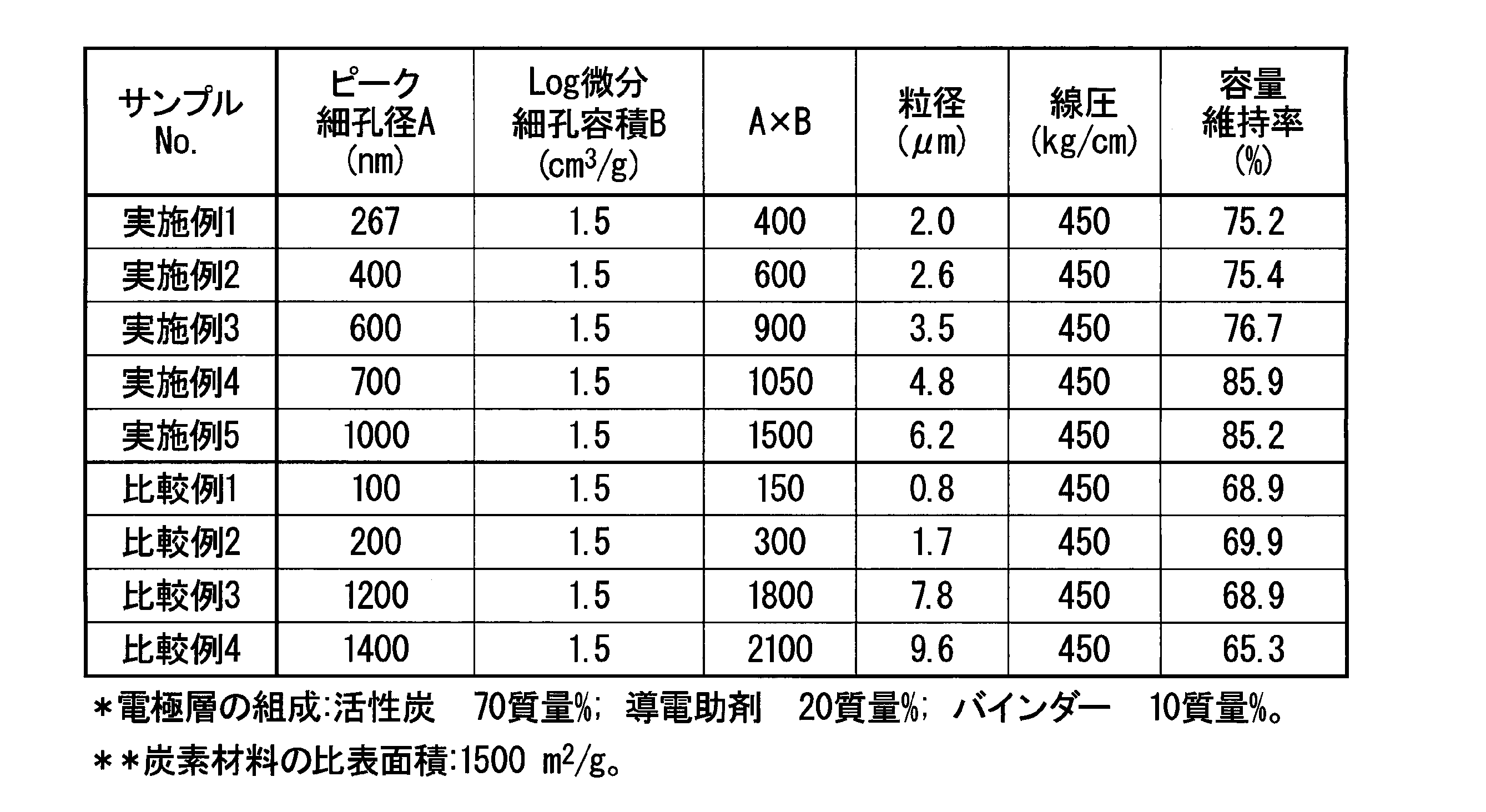
(実施例1~5及び比較例1~4)
[電極の作製]
活物質である炭素材料はBET法による比表面積が約1500m2/gの活性炭(粒径が表1に示す。)を使用し、導電助剤としてはカーボンブラック粉末を使用し、バインダーとしてはポリフッ化ビニリデン(PVDF)を使用し、炭素材料と導電助剤とバインダーの質量比率を炭素材料:導電助剤:バインダー=70:20:10となるように配合し、スラリーを調製した。得られたスラリーを厚さ20μmのアルミ箔上に塗工し、温度140℃で30分間乾燥した後にロールプレス装置によりプレス処理して、電極を得た。厚みの測定はマイクロメーターを用いた。ロールプレスの条件は、線圧を450kgf/cm、加熱ロール温度は室温、送り速度を5m/minとした。線圧は加圧ロールに掛かる圧力と上下のロールが接触する長さで計算をした。
(Examples 1 to 5 and Comparative Examples 1 to 4)
[Preparation of electrode]
Activated carbon having a specific surface area of about 1500 m 2 /g by the BET method (particle size is shown in Table 1) was used as the carbon material as the active material, carbon black powder was used as the conductive aid, and polyfluoride was used as the binder. A slurry was prepared by using vinylidene chloride (PVDF) and blending the carbon material, the conductive aid, and the binder so that the mass ratio of the carbon material:conductive aid:binder=70:20:10. The resulting slurry was applied onto an aluminum foil having a thickness of 20 μm, dried at 140° C. for 30 minutes, and pressed with a roll press to obtain an electrode. A micrometer was used to measure the thickness. The roll press conditions were a line pressure of 450 kgf/cm, a heating roll temperature of room temperature, and a feed rate of 5 m/min. The linear pressure was calculated by the pressure applied to the pressure roll and the length of contact between the upper and lower rolls.
<ピーク細孔径AとLog微分細孔容積Bの評価>
作製した電極の電極層の細孔分布を、水銀ポロシメータを用いて水銀圧入法により測定し、図2に示したようなLog微粉細孔容積分布グラフを得た。得られたLog微粉細孔容積分布グラフから、ピーク細孔径Aとピーク細孔径AにおけるLog微分細孔容積Bを読み取り、その積A×Bを求めた。その結果を、使用された炭素材料の粒径、ロールプレスの条件とともに表1に示す。
<Evaluation of Peak Pore Diameter A and Log Differential Pore Volume B>
The pore distribution of the electrode layer of the produced electrode was measured by the mercury intrusion method using a mercury porosimeter to obtain a log fine powder pore volume distribution graph as shown in FIG. From the obtained log fine powder pore volume distribution graph, the peak pore diameter A and the log differential pore volume B at the peak pore diameter A were read, and the product A×B was obtained. The results are shown in Table 1 together with the particle size of the carbon material used and the conditions of roll pressing.
[非水電解液]
アセトニトリル(AN)に、テトラエチルアンモニウムテトラフルオロボレートを1.0mol/Lとなるように溶解させた非水電解液を用意した。
[Non-aqueous electrolyte]
A non-aqueous electrolytic solution was prepared by dissolving tetraethylammonium tetrafluoroborate in acetonitrile (AN) so as to have a concentration of 1.0 mol/L.
[セパレータ]
膜厚20μmのポリエチレン微多孔膜を用意した。
[Separator]
A polyethylene microporous membrane having a thickness of 20 μm was prepared.
[電気二重層キャパシタの作製]
上記で得られた電極2枚をそれぞれ12.5cm2になるように切り取り、正極、負極とした。この正極、負極それぞれに正極端子と負極端子とを超音波融着して、正極と負極の間に上記セパレータを挟むように積層させ巻回した後、外装体としてのアルミラミネート材で覆い、上記非水電解液を注入し、最後に開口部を融着密封することにより、単セルの電気二重層キャパシタを作製した。これを2組作製し、直列になるように接続して実施例1~5及び比較例1~4の電気二重層キャパシタを作製した。作製した実施例1~5及び比較例1~4の電気二重層キャパシタは、直列に接続された2つの単セルを含むが、1つのセルとして容量維持率の評価を行った。
[Production of electric double layer capacitor]
Each of the two electrodes obtained above was cut into pieces of 12.5 cm 2 to form a positive electrode and a negative electrode. A positive electrode terminal and a negative electrode terminal are ultrasonically fused to each of the positive electrode and the negative electrode, and the separator is sandwiched between the positive electrode and the negative electrode. A single-cell electric double layer capacitor was fabricated by injecting a non-aqueous electrolyte and finally sealing the opening by fusion bonding. Two sets of these were produced and connected in series to produce electric double layer capacitors of Examples 1 to 5 and Comparative Examples 1 to 4. The produced electric double layer capacitors of Examples 1 to 5 and Comparative Examples 1 to 4 include two single cells connected in series, and the capacity retention rate was evaluated as one cell.
<容量維持率の評価>
実施例1~5及び比較例1~4の電気二重層キャパシタについて、50mAで5.7Vまで定電流充電を行い、5.7Vに達した後は定電圧充電に移行し、1秒間定電圧充電を行った。放電は50mAの定電流で行い、終止電圧0.1Vとした。これにより得られた放電曲線(放電電圧-放電時間)から、5.0Vから3.0Vまでにかかった時間Δt[msec.]を求め、下記の関係式:
容量={放電電流(50mA)×時間Δt}/電圧(5.0-3.0V)
により初回容量値(C0)を算出した。
<Evaluation of Capacity Retention Rate>
For the electric double layer capacitors of Examples 1 to 5 and Comparative Examples 1 to 4, constant current charging was performed at 50 mA to 5.7 V, and after reaching 5.7 V, constant voltage charging was performed, and constant voltage charging was performed for 1 second. did Discharging was performed at a constant current of 50 mA and a final voltage of 0.1V. From the discharge curve (discharge voltage-discharge time) thus obtained, the time Δt [msec. ] and the following relational expression:
Capacity = {discharge current (50mA) x time Δt} / voltage (5.0-3.0V)
The initial capacity value (C 0 ) was calculated by
初期容量値を測定後、80℃に設定した恒温槽内で5.0Vの電圧を掛けることで試料に負荷を与えた。80℃、5.0V負荷で2000h経過後、上記と同様に容量(C2000)を算出した。そして、初回容量値(C0)に対する容量値(C2000)の割合(=C2000/C0×100)を容量維持率(%)として算出した。その結果を表1に示す。なお、容量維持率が70%以上の場合を良好なものであり、容量維持率が85%以上の場合を優れたものであると判断した。 After measuring the initial capacity value, a load was applied to the sample by applying a voltage of 5.0 V in a constant temperature bath set at 80°C. After 2000 hours at 80° C. and 5.0 V load, the capacity (C 2000 ) was calculated in the same manner as above. Then, the ratio of the capacity value (C 2000 ) to the initial capacity value (C 0 ) (=C 2000 /C 0 ×100) was calculated as the capacity retention rate (%). Table 1 shows the results. A case where the capacity retention rate was 70% or more was judged to be good, and a case where the capacity retention rate was 85% or more was judged to be excellent.
<平均粒径の測定>
炭素材料の平均粒径(粒度分布)は、レーザー散乱法による以下の通りに測定した。試料を界面活性剤(和光純薬工業(株)製「TritonX100」)が0.3質量%含まれた水溶液に投入し、超音波洗浄器で10分以上処理し、水溶液中に分散させた。この分散液を用いて粒度分布を測定した。粒度分布測定は、粒径・粒度分布測定器(日機装(株)製「マイクロトラックMT3000」)を用いて行った。D50は、累積体積が50%となる粒径であり、この値を平均粒径として用いた。
<Measurement of average particle size>
The average particle size (particle size distribution) of the carbon material was measured by a laser scattering method as follows. The sample was put into an aqueous solution containing 0.3% by mass of a surfactant (“Triton X100” manufactured by Wako Pure Chemical Industries, Ltd.), treated with an ultrasonic cleaner for 10 minutes or more, and dispersed in the aqueous solution. The particle size distribution was measured using this dispersion. The particle size distribution was measured using a particle size/particle size distribution analyzer ("Microtrac MT3000" manufactured by Nikkiso Co., Ltd.). D50 is the particle size at which the cumulative volume is 50%, and this value was used as the average particle size.
<BET比表面積測定>
カンタクローム・インスツルメンツ社製高速・比表面積/細孔分布測定装置NOVA4200eを使用し、活物質である炭素材料の窒素吸着等温線を測定するBET法により比表面積を求めた。
<BET specific surface area measurement>
The specific surface area was determined by the BET method for measuring the nitrogen adsorption isotherm of the active carbon material using a high-speed specific surface area/pore size distribution analyzer NOVA4200e manufactured by Quantachrome Instruments.
(実施例6~11及び比較例5~8)
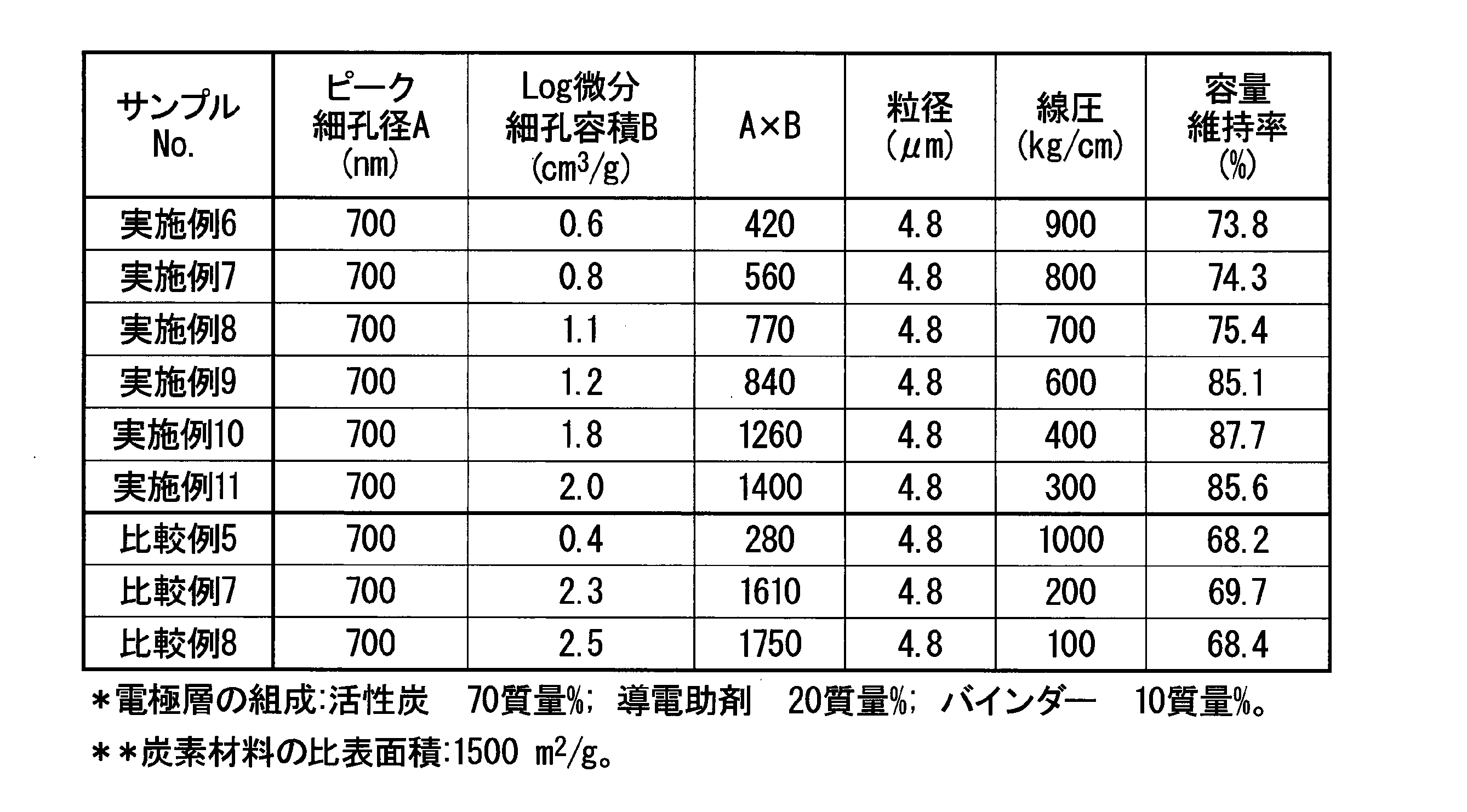
表2に示すように、ロールプレスの線圧が100~1000kgf/cmである以外は、実施例4と同様に電気二重層キャパシタを作製した。
実施例4と同様に得られた電気二重層キャパシタの電極層及び電気二重層キャパシタを評価し、その結果を表2に示す。
(Examples 6-11 and Comparative Examples 5-8)
As shown in Table 2, electric double layer capacitors were produced in the same manner as in Example 4, except that the linear pressure of the roll press was 100 to 1000 kgf/cm.
The electrode layer of the electric double layer capacitor and the electric double layer capacitor obtained in the same manner as in Example 4 were evaluated, and the results are shown in Table 2.
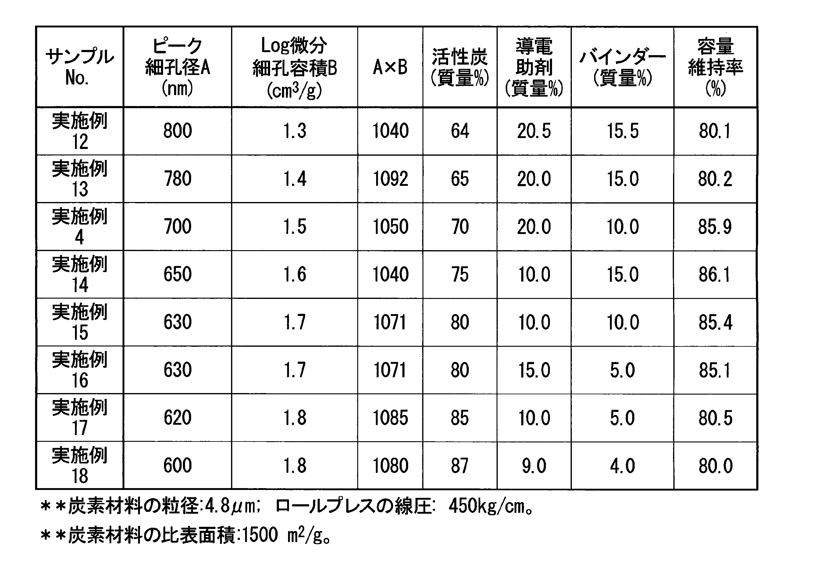
(実施例12~18)
表3に示すように、炭素材料と導電助剤とバインダーの質量比率を炭素材料:導電助剤:バインダー=64:20.5:15.5~87:9.0:4.0となるように配合した以外は、実施例4と同様に電気二重層キャパシタを作製した。
実施例4と同様に得られた電気二重層キャパシタ用電極の電極層及び電気二重層キャパシタを評価し、その結果を表3に示す。
(Examples 12-18)
As shown in Table 3, the mass ratio of the carbon material, the conductive aid, and the binder was adjusted to carbon material: conductive aid: binder = 64: 20.5: 15.5 to 87: 9.0: 4.0. An electric double layer capacitor was produced in the same manner as in Example 4, except that
The electrode layer of the electrode for an electric double layer capacitor and the electric double layer capacitor obtained in the same manner as in Example 4 were evaluated, and the results are shown in Table 3.
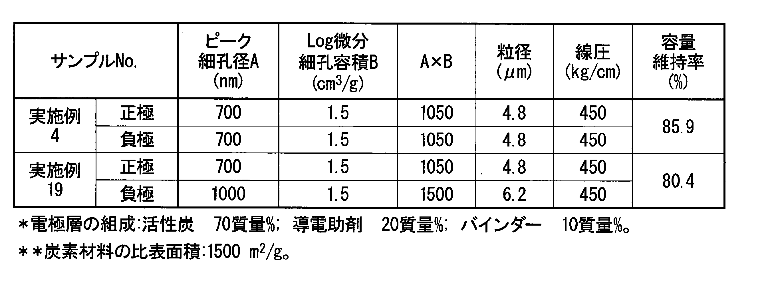
(実施例19)
表4に示すように、正極が実施例4の電気二重層キャパシタ用電極を用い、負極が実施例5の電気二重層キャパシタ用電極を用いた以外は、実施例4と同様に電気二重層キャパシタを作製した。
実施例4と同様に得られた電気二重層キャパシタの電極層及び電気二重層キャパシタを評価し、その結果を表4に示す。
(Example 19)
As shown in Table 4, the same electric double layer capacitor as in Example 4 was used except that the positive electrode used the electric double layer capacitor electrode of Example 4 and the negative electrode used the electric double layer capacitor electrode of Example 5. was made.
The electrode layer of the electric double layer capacitor and the electric double layer capacitor obtained in the same manner as in Example 4 were evaluated, and the results are shown in Table 4.
(実施例20~27)
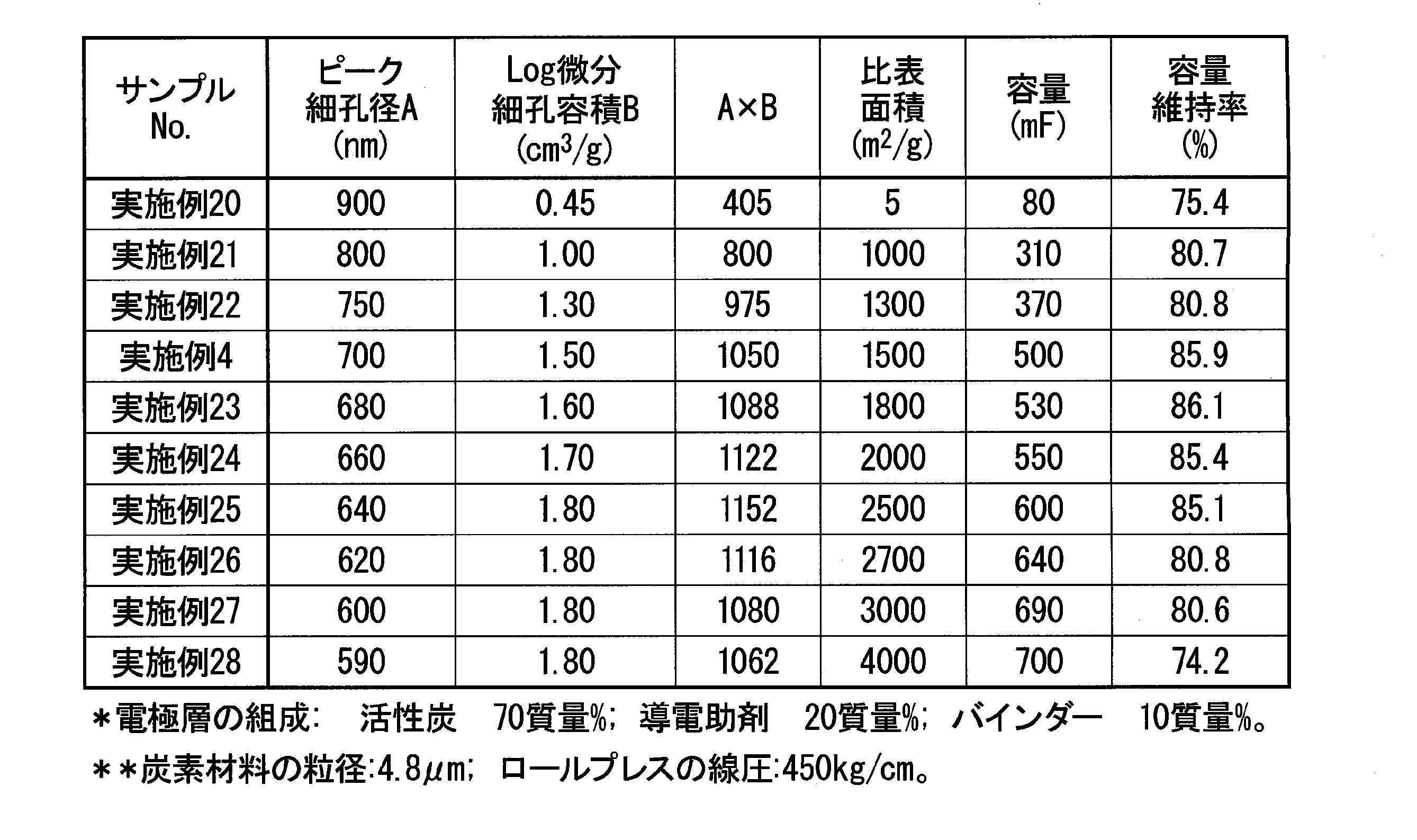
表5に示すように、比表面積が5~4000m2/gの炭素材料を用いた以外は、実施例4と同様に電気二重層キャパシタを作製した。
実施例4と同様に得られた電気二重層キャパシタの電極層及び電気二重層キャパシタを評価し、その結果を表5に示す。また、初回容量値を容量とし、表5に示す。
(Examples 20-27)
As shown in Table 5, an electric double layer capacitor was produced in the same manner as in Example 4 except that a carbon material having a specific surface area of 5 to 4000 m 2 /g was used.
The electrode layer of the electric double layer capacitor and the electric double layer capacitor obtained in the same manner as in Example 4 were evaluated, and the results are shown in Table 5. Table 5 shows the initial capacity value as the capacity.
10…セパレータ、20…正極(電気二重層キャパシタ用電極)、22…正極集電体(集電体)、24…正極活物質層(電極層)、30…負極(電気二重層キャパシタ用電極)、32…負極集電体(集電体)、34…負極活物質層(電極層)、40…発電要素、50…外装体、52…金属箔、54…高分子膜、60,62…リード、100…電気二重層キャパシタ
DESCRIPTION OF
Claims (5)
前記電極層は、
炭素材料を65質量%以上85質量%以下の範囲内、
導電助剤を10質量%以上20質量%以下の範囲内、
バインダーを5質量%以上15質量%以下の範囲内で含有し、
前記導電助剤と前記バインダーの合計が20質量%以上、30質量%以下であり、
前記バインダーが、ポリフッ化ビニリデンであり、
前記電極層において水銀圧入法によって得られたLog微分細孔容積分布グラフにおいて、ピーク細孔径A(単位:nm)と、前記ピーク細孔径AにおけるLog微分細孔容積B(単位:cm3/g)との積A×Bが、400以上、1500以下であり、
前記ピーク細孔径Aが630nm以上、1000nm以下の範囲に存在し、
前記ピーク細孔径AにおけるLog微分細孔容積Bが0.8cm 3 /g以上、2cm 3 /g以下である
ことを特徴とする電気二重層キャパシタ用電極。 having a current collector and an electrode layer formed on the current collector;
The electrode layer is
Within the range of 65% by mass or more and 85% by mass or less of the carbon material,
Within the range of 10% by mass or more and 20% by mass or less of the conductive aid,
Containing a binder in the range of 5% by mass or more and 15% by mass or less,
The total amount of the conductive aid and the binder is 20% by mass or more and 30% by mass or less,
The binder is polyvinylidene fluoride,
In the log differential pore volume distribution graph obtained by the mercury intrusion method in the electrode layer, the peak pore diameter A (unit: nm) and the log differential pore volume B at the peak pore diameter A (unit: cm 3 /g ) and the product A × B is 400 or more and 1500 or less,
The peak pore diameter A is present in the range of 630 nm or more and 1000 nm or less,
Log differential pore volume B at the peak pore diameter A is 0.8 cm 3 /g or more and 2 cm 3 /g or less
An electrode for an electric double layer capacitor characterized by:
ことを特徴とする請求項1に記載の電気二重層キャパシタ用電極。 2. The electrode for an electric double layer capacitor according to claim 1, wherein the carbon material has a specific surface area of 1000 m <2> /g or more and 3000 m <2> /g or less.
非水電解液と
を有することを特徴とする電気二重層キャパシタ。 The electric double layer capacitor electrode according to claim 1 or 2 ,
and a non-aqueous electrolyte.
前記正極が前記電気二重層キャパシタ用電極からなる第一の電極を用い、
前記負極が前記電気二重層キャパシタ用電極からなる第二の電極を用い、
前記第一の電極と前記第二の電極が同一である
ことを特徴とする請求項3に記載の電気二重層キャパシタ。 having a positive electrode and a negative electrode,
Using a first electrode in which the positive electrode is the electrode for the electric double layer capacitor,
Using a second electrode in which the negative electrode is the electrode for the electric double layer capacitor,
4. The electric double layer capacitor according to claim 3 , wherein said first electrode and said second electrode are the same.
前記2つ以上の単セルが直列に接続されている
ことを特徴とする請求項4に記載の電気二重層キャパシタ。 The electric double layer capacitor includes two or more single cells each having the positive electrode and the negative electrode,
5. The electric double layer capacitor according to claim 4 , wherein the two or more single cells are connected in series.
Priority Applications (1)
| Application Number | Priority Date | Filing Date | Title |
|---|---|---|---|
| JP2018174962A JP7305940B2 (en) | 2018-09-19 | 2018-09-19 | Electrodes for electric double layer capacitors and electric double layer capacitors |
Applications Claiming Priority (1)
| Application Number | Priority Date | Filing Date | Title |
|---|---|---|---|
| JP2018174962A JP7305940B2 (en) | 2018-09-19 | 2018-09-19 | Electrodes for electric double layer capacitors and electric double layer capacitors |
Publications (2)
| Publication Number | Publication Date |
|---|---|
| JP2020047764A JP2020047764A (en) | 2020-03-26 |
| JP7305940B2 true JP7305940B2 (en) | 2023-07-11 |
Family
ID=69899937
Family Applications (1)
| Application Number | Title | Priority Date | Filing Date |
|---|---|---|---|
| JP2018174962A Active JP7305940B2 (en) | 2018-09-19 | 2018-09-19 | Electrodes for electric double layer capacitors and electric double layer capacitors |
Country Status (1)
| Country | Link |
|---|---|
| JP (1) | JP7305940B2 (en) |
Families Citing this family (4)
| Publication number | Priority date | Publication date | Assignee | Title |
|---|---|---|---|---|
| KR102885686B1 (en) * | 2020-02-28 | 2025-11-12 | 니폰 제온 가부시키가이샤 | carbon film |
| CN116457307B (en) * | 2020-11-30 | 2024-08-16 | 日本瑞翁株式会社 | Carbon film |
| JP2023069303A (en) * | 2021-11-05 | 2023-05-18 | パナソニックIpマネジメント株式会社 | Capacitor |
| JPWO2023189140A1 (en) * | 2022-03-30 | 2023-10-05 |
Citations (6)
| Publication number | Priority date | Publication date | Assignee | Title |
|---|---|---|---|---|
| JP2008211176A (en) | 2007-02-01 | 2008-09-11 | Hitachi Chem Co Ltd | Metal thin film having more than one through hole, its manufacturing method, and electric double-layer capacitor |
| JP2009048876A (en) | 2007-08-21 | 2009-03-05 | Hitachi Maxell Ltd | Non-aqueous secondary battery |
| JP2010157564A (en) | 2008-12-26 | 2010-07-15 | Nippon Zeon Co Ltd | Method of manufacturing composite particle for electrochemical element electrode |
| JP2014072348A (en) | 2012-09-28 | 2014-04-21 | Tdk Corp | Electrochemical device |
| JP2016152153A (en) | 2015-02-18 | 2016-08-22 | 株式会社Gsユアサ | Power storage element and method of manufacturing power storage element |
| JP2018147672A (en) | 2017-03-03 | 2018-09-20 | Tdk株式会社 | Negative electrode and lithium ion secondary battery |
-
2018
- 2018-09-19 JP JP2018174962A patent/JP7305940B2/en active Active
Patent Citations (6)
| Publication number | Priority date | Publication date | Assignee | Title |
|---|---|---|---|---|
| JP2008211176A (en) | 2007-02-01 | 2008-09-11 | Hitachi Chem Co Ltd | Metal thin film having more than one through hole, its manufacturing method, and electric double-layer capacitor |
| JP2009048876A (en) | 2007-08-21 | 2009-03-05 | Hitachi Maxell Ltd | Non-aqueous secondary battery |
| JP2010157564A (en) | 2008-12-26 | 2010-07-15 | Nippon Zeon Co Ltd | Method of manufacturing composite particle for electrochemical element electrode |
| JP2014072348A (en) | 2012-09-28 | 2014-04-21 | Tdk Corp | Electrochemical device |
| JP2016152153A (en) | 2015-02-18 | 2016-08-22 | 株式会社Gsユアサ | Power storage element and method of manufacturing power storage element |
| JP2018147672A (en) | 2017-03-03 | 2018-09-20 | Tdk株式会社 | Negative electrode and lithium ion secondary battery |
Also Published As
| Publication number | Publication date |
|---|---|
| JP2020047764A (en) | 2020-03-26 |
Similar Documents
| Publication | Publication Date | Title |
|---|---|---|
| US6349027B1 (en) | Electric double layer capacitor | |
| US9997301B2 (en) | Electrode, electric double-layer capacitor using the same, and manufacturing method of the electrode | |
| JP7305940B2 (en) | Electrodes for electric double layer capacitors and electric double layer capacitors | |
| US20100220429A1 (en) | Electric Double Layer Capacitor | |
| US9951443B2 (en) | Separators, electrodes, half-cells, and cells of electrical energy storage devices | |
| JP6375593B2 (en) | Electrode, electric double layer capacitor using the electrode, and method for manufacturing electrode | |
| JP5302646B2 (en) | Pre-doping power storage device | |
| US20190172655A1 (en) | Carbon material, electrode sheet for capacitor, and capacitor | |
| JP6428628B2 (en) | Method for producing composite particles for electrochemical devices | |
| JP2013135223A (en) | Electrode active material-conductive agent composite, method for preparing the same, and electrochemical capacitor comprising the same | |
| JP2006324286A (en) | Method for producing electrode for electrochemical capacitor | |
| KR101331966B1 (en) | Electrochemical capacitor | |
| JP2013098575A (en) | Electrode active material composition and method of manufacturing the same, and electrochemical capacitor with the same | |
| JP2013065851A (en) | Electrode active material, method for preparing the same, and electrochemical capacitor including the same | |
| KR20150037844A (en) | Polarizable electrode material and electric double layer capacitor using same | |
| JP2020136487A (en) | Electric double layer capacitor | |
| CN1866431B (en) | Electrochemical capacitor electrode production method | |
| JP2004186275A (en) | Electrode sheet for electric double layer capacitor, method for producing the same, polarizable electrode and electric double layer capacitor using polarizable electrode | |
| EP0938109A2 (en) | Electric double layer capacitor | |
| JP7425983B2 (en) | Electrodes for electric double layer capacitors and electric double layer capacitors | |
| JP2020064971A (en) | Active material for electric double layer capacitor, electrode for electric double layer capacitor, and electric double layer capacitor | |
| JP2008010613A (en) | Electric double layer capacitor | |
| JP2008130740A (en) | Electrode for electric double layer capacitor and method for manufacturing the same | |
| JP6179195B2 (en) | Electric double layer capacitor | |
| JP2007335443A (en) | Electric double layer capacitor coated electrode slurry, electric double layer capacitor sheet and electric double layer capacitor |
Legal Events
| Date | Code | Title | Description |
|---|---|---|---|
| A621 | Written request for application examination |
Free format text: JAPANESE INTERMEDIATE CODE: A621 Effective date: 20210423 |
|
| A977 | Report on retrieval |
Free format text: JAPANESE INTERMEDIATE CODE: A971007 Effective date: 20220421 |
|
| A131 | Notification of reasons for refusal |
Free format text: JAPANESE INTERMEDIATE CODE: A131 Effective date: 20220510 |
|
| A601 | Written request for extension of time |
Free format text: JAPANESE INTERMEDIATE CODE: A601 Effective date: 20220708 |
|
| A521 | Request for written amendment filed |
Free format text: JAPANESE INTERMEDIATE CODE: A523 Effective date: 20220908 |
|
| A02 | Decision of refusal |
Free format text: JAPANESE INTERMEDIATE CODE: A02 Effective date: 20230117 |
|
| A521 | Request for written amendment filed |
Free format text: JAPANESE INTERMEDIATE CODE: A523 Effective date: 20230414 |
|
| C60 | Trial request (containing other claim documents, opposition documents) |
Free format text: JAPANESE INTERMEDIATE CODE: C60 Effective date: 20230414 |
|
| A911 | Transfer to examiner for re-examination before appeal (zenchi) |
Free format text: JAPANESE INTERMEDIATE CODE: A911 Effective date: 20230424 |
|
| C21 | Notice of transfer of a case for reconsideration by examiners before appeal proceedings |
Free format text: JAPANESE INTERMEDIATE CODE: C21 Effective date: 20230425 |
|
| TRDD | Decision of grant or rejection written | ||
| A01 | Written decision to grant a patent or to grant a registration (utility model) |
Free format text: JAPANESE INTERMEDIATE CODE: A01 Effective date: 20230530 |
|
| A61 | First payment of annual fees (during grant procedure) |
Free format text: JAPANESE INTERMEDIATE CODE: A61 Effective date: 20230612 |
|
| R150 | Certificate of patent or registration of utility model |
Ref document number: 7305940 Country of ref document: JP Free format text: JAPANESE INTERMEDIATE CODE: R150 |