JP7260372B2 - Method for manufacturing substrate for mounting semiconductor device - Google Patents
Method for manufacturing substrate for mounting semiconductor device Download PDFInfo
- Publication number
- JP7260372B2 JP7260372B2 JP2019070791A JP2019070791A JP7260372B2 JP 7260372 B2 JP7260372 B2 JP 7260372B2 JP 2019070791 A JP2019070791 A JP 2019070791A JP 2019070791 A JP2019070791 A JP 2019070791A JP 7260372 B2 JP7260372 B2 JP 7260372B2
- Authority
- JP
- Japan
- Prior art keywords
- metal plate
- semiconductor element
- columnar
- substrate
- mounting
- Prior art date
- Legal status (The legal status is an assumption and is not a legal conclusion. Google has not performed a legal analysis and makes no representation as to the accuracy of the status listed.)
- Active
Links
Images


Classifications
-
- H10W72/0198—
-
- H10W74/00—
-
- H10W90/724—
-
- H10W90/756—
Landscapes
- Lead Frames For Integrated Circuits (AREA)
Description
本発明は、半導体素子が搭載された領域を封止樹脂で封止した樹脂封止体から金属板を除去することによって製造され、裏面側に露出するめっき層からなる外部接続用端子がプリント基板等の外部機器と接続されるタイプの半導体パッケージの製造に用いる半導体素子搭載用基板の製造方法に関する。 The present invention is manufactured by removing a metal plate from a resin sealing body in which a region where a semiconductor element is mounted is sealed with a sealing resin, and an external connection terminal made of a plating layer exposed on the back side is a printed circuit board. The present invention relates to a method for manufacturing a substrate for mounting a semiconductor element used for manufacturing a semiconductor package of a type connected to an external device such as.
半導体装置の電子関連機器への組み込みに際し、半導体装置の外部接続用端子と、外部の電子関連機器との半田接続状態の良・不良を目視で検査できるように、半田接続部分の可視化が求められている。 When a semiconductor device is incorporated into an electronic device, there is a demand for visualization of solder joints so that it is possible to visually inspect whether the solder connection between the external connection terminal of the semiconductor device and the external electronic device is good or bad. ing.
しかるに、従来、外周部に外部接続用端子が突出しないタイプの半導体パッケージは、裏面側に露出した状態に配列されている複数の外部接続用端子をプリント基板等の外部機器と接続する構造となっていたため、正常に半田接続されているか否かを目視検査することが困難であった。 Conventionally, however, a semiconductor package of a type in which external connection terminals do not protrude from the outer peripheral portion has a structure in which a plurality of external connection terminals arranged in an exposed state on the back side are connected to an external device such as a printed circuit board. Therefore, it was difficult to visually inspect whether the solder connection was normal.
しかし、半田接続部分の目視検査ができないと、半田接続作業時に内在する接続不良が見逃され、その後の通電検査等で接続不良が発見されるまでの作業コストが余計にかかってしまう。また、半田接続部分は、X線装置を用いて透視検査することは可能ではあるが、それでは、X線装置の設備コストが増大してしまう。 However, if a visual inspection of the soldered connection portion is not possible, the connection failure inherent in the soldering work will be overlooked, and the work cost until the connection failure is discovered in the subsequent energization inspection or the like will be extra. Also, although it is possible to carry out a fluoroscopic inspection of the soldered joint using an X-ray apparatus, this would increase the equipment cost of the X-ray apparatus.
そこで、従来、半導体パッケージの半田接続部分における半田接続状態の良・不良を目視検査できるようにするための技術として、例えば、次の特許文献1には、リードフレームにおけるリードの裏面側の外部接続用端子となる端子部の切断位置にリードを横断する溝を形成することで、個々に切断されたときの半導体パッケージの裏面に露出する外部接続用端子に、端縁部にかけて空間部を設け、空間部に半田を介在させるようにして、半導体パッケージの側面に露出した外部接続用端子の端縁部から半田接続部分を目視可能にすることが提案されている。
Therefore, conventionally, as a technique for visually inspecting whether the soldered connection state in the soldered connection part of the semiconductor package is good or bad, for example, the following
また、例えば、次の特許文献2には、リードフレームの裏面に凹部を設け、表面側を樹脂封止後に、凹部を含む所定領域を封止樹脂側からハーフカット加工を施すことで、凹部を設けていた部位にスルーホールを形成し、次に、ハーフカット加工の幅より狭い幅でフルカット加工を施すことで、外部接続用端子を側方に突出させ、側方の突出部に、半田接続部分を目視可能にするためのスルーホールやスリットを設けることが記載されている。 Further, for example, in the following Patent Document 2, a concave portion is provided on the back surface of a lead frame, and after the front side is sealed with resin, a predetermined region including the concave portion is subjected to half-cut processing from the sealing resin side, thereby forming the concave portion. A through-hole is formed in the previously provided portion, and then full-cut processing is performed with a width narrower than the width of the half-cut processing, so that the external connection terminal protrudes laterally, and solder is applied to the protruding portion on the side. It is described that a through hole or a slit is provided to make the connection part visible.
しかし、特許文献1に記載のリードフレームにおけるリードの裏面側の外部接続用端子となる端子部の切断位置にリードを横断する溝を形成する技術では、樹脂封止の際に、端子部の溝に樹脂が入り込み、半田接続部分を目視可能にするための空間部が形成されず、半導体パッケージ製品の歩留まりが悪くなる虞がある。
However, in the technique of forming a groove that traverses the lead at the cutting position of the terminal portion that will be the external connection terminal on the back side of the lead in the lead frame described in
また、特許文献2に記載の技術では、樹脂封止後に、ブレードを用いたハーフカットとフルカットの2回の切断工程が必要となり、生産効率が悪く、コストが増大してしまう。また、外部接続用端子が側方へ突出するため、半導体パッケージ製品を小型化し難い。 In addition, the technique described in Patent Document 2 requires two cutting processes, half-cutting and full-cutting, using a blade after resin encapsulation, resulting in poor production efficiency and an increase in cost. In addition, since the external connection terminals protrude laterally, it is difficult to miniaturize the semiconductor package product.
このように、裏面側に露出している複数の外部接続用端子をプリント基板等の外部機器と接続するタイプの半導体パッケージにおける、半田接続部分を目視可能とするための従来技術には、半導体パッケージ製品の歩留まりや、生産効率、製品の小型化の点で問題があった。 As described above, in a semiconductor package of a type in which a plurality of external connection terminals exposed on the back side are connected to an external device such as a printed circuit board, conventional techniques for making the solder connection portions visible include: There were problems in terms of product yield, production efficiency, and product miniaturization.
この問題に対し、本件発明者は、半導体パッケージ製品の歩留まりや、生産効率が向上し、小型化にも対応でき、しかも、裏面側に露出している複数の外部接続用端子を外部機器と接続するタイプの半導体パッケージにおける、半田接合部分における半田接続状態の良・不良を目視検査可能にするリードフレームとして、リードフレームにおけるリードの裏面側の外部接続端子部の切断位置に、凹部を形成する構成を着想した。 In response to this problem, the inventors of the present invention have improved the yield and production efficiency of semiconductor package products, are able to respond to miniaturization, and moreover, connect a plurality of external connection terminals exposed on the back side to external devices. As a lead frame for enabling visual inspection of good/bad solder connections in solder joints in a semiconductor package of the type to was conceived.
しかし、リードの裏面側の外部接続端子部の切断位置に、凹部を形成した構成のリードフレームには、半導体パッケージを製造後に個片化するための切断により金属屑が凹部に付着してしまう問題があることが判明した。 However, there is a problem that metal scraps adhere to the recess when the semiconductor package is cut into individual pieces after the semiconductor package is manufactured in the lead frame having the configuration in which the recess is formed at the cutting position of the external connection terminal portion on the back side of the lead. It turned out that there is
そこで、本件発明者は、半導体素子が搭載された領域を封止樹脂で封止した樹脂封止体から金属板を除去することによって製造され、裏面側に露出するめっき層からなる外部接続用端子がプリント基板等の外部機器と接続されるタイプの半導体パッケージの製造に用いる半導体素子搭載用基板について検討した。そして、試行錯誤の末、金属板に凹部を設けることによって柱状突起部を形成し、柱状突起部の側面および上面と凹部の底面における柱状突起部の周囲の所定領域をめっき層で覆い、金属板を除去した時に、めっき層の断面が門形状になるようにした構成の半導体素子搭載用基板を導出した。 Therefore, the inventors of the present invention have proposed an external connection terminal made of a plating layer exposed on the back side, which is manufactured by removing a metal plate from a resin sealing body in which a region where a semiconductor element is mounted is sealed with a sealing resin. A substrate for mounting a semiconductor device used in the manufacture of a semiconductor package that is connected to an external device such as a printed circuit board was investigated. Then, after trial and error, the metal plate is provided with recesses to form the columnar protrusions, and the side and top surfaces of the columnar protrusions and predetermined regions around the columnar protrusions on the bottom surface of the recesses are covered with a plating layer, and the metal plate is A substrate for mounting a semiconductor device having a configuration in which the cross section of the plating layer becomes gate-shaped when the is removed was derived.
さらに、本件発明者が、導出した半導体素子搭載用基板について試行錯誤を重ねたところ、半田接続部分を目視し易くするためには、めっき層からなる外部接続端子の門形状の内側部分の高さを所定以上にする必要があることが判明した。 Further, the inventors of the present invention repeated trial and error with respect to the semiconductor element mounting substrate derived, and found that the height of the gate-shaped inner portion of the external connection terminal made of the plating layer was It was found that it is necessary to set the
そこで、本件発明者は、柱状突起部の高さを所定以上にした半導体素子搭載用基板を製造し、更に、試行錯誤を重ねた。
その結果、所定以上の高さの柱状突起部を備えた半導体素子搭載用基板を製造する場合、レジストフィルムを金属板に圧着することによって、外部接続端子用のめっき層を形成するためのめっき用レジストマスクを形成すると、レジストフィルムが柱状突起部の高さに追従できず、レジストフィルムと柱状突起部が形成された金属板との間に気泡が残り、レジストフィルムを圧着後に形成したレジストマスクの開口部からめっき層を形成した際に、めっき層の被膜にボイド不良を生じ易く、歩留まりが悪化し、生産性が低下することが判明した。
Therefore, the inventor of the present invention manufactured a substrate for mounting a semiconductor element having a columnar projection with a predetermined height or more, and repeated trial and error.
As a result, in the case of manufacturing a substrate for mounting a semiconductor element having columnar protrusions with a height higher than a predetermined height, a plating layer for forming a plating layer for external connection terminals can be obtained by crimping a resist film onto a metal plate. When the resist mask was formed, the resist film could not follow the height of the columnar protrusions, and air bubbles remained between the resist film and the metal plate on which the columnar protrusions were formed. It has been found that when the plating layer is formed from the opening, void defects are likely to occur in the film of the plating layer, resulting in deterioration of yield and productivity.
本発明は、上記従来の課題を鑑みてなされたものであり、半導体素子が搭載された領域を封止樹脂で封止した樹脂封止体から金属板を除去することによって製造され、裏面側に露出するめっき層からなる外部接続用端子がプリント基板等の外部機器と接続されるタイプの半導体パッケージの製造に用いる半導体素子搭載用基板であって、半導体パッケージ製品の歩留まりや、生産効率を向上させ、小型化にも対応でき、しかも、半田接続部分を目視可能にする半導体素子搭載用基板の製造方法において、コストを抑えながら、外部接続用端子をなすめっき層の被膜のボイド不良を防止し、半導体素子搭載用基板の歩留まりや、生産性を向上させることの可能な半導体素子搭載用基板の製造方法を提供することを目的としている。 The present invention has been made in view of the above-described conventional problems, and is manufactured by removing a metal plate from a resin sealing body in which a region where a semiconductor element is mounted is sealed with a sealing resin, and A substrate for mounting a semiconductor element used in the manufacture of a type of semiconductor package in which external connection terminals made of an exposed plating layer are connected to an external device such as a printed circuit board, improving the yield and production efficiency of semiconductor package products. In a method for manufacturing a substrate for mounting a semiconductor element, which can cope with miniaturization and allows visual observation of soldered connection parts, while suppressing costs, void defects in the film of the plating layer forming external connection terminals are prevented, It is an object of the present invention to provide a method of manufacturing a substrate for mounting a semiconductor element capable of improving yield and productivity of the substrate for mounting a semiconductor element.
上記目的を達成するため、本発明の一態様による半導体素子搭載用基板の製造方法は、複数の半導体素子搭載用基板が多列配置され、個々の半導体素子搭載用基板が、金属板の一方の側の面に凹部を設けることによって形成され、半導体パッケージ領域の内側で四方の縁部から中央に向かって細長状に延びた、0.10mm以上0.18mm以下の高さの複数の柱状突起部と、夫々の前記柱状突起部の側面および上面と前記凹部の底面における前記柱状突起部の周囲の所定領域を覆う、めっき層からなる複数の端子部と、を有する半導体素子搭載用基板の製造方法であって、前記金属板の一方の側の面上に、前記凹部に対応する領域を開口する開口部を有し、複数の前記柱状突起部に対応する領域を覆うエッチング用レジストマスクを形成するとともに、前記金属板の他方の側の面上に、全面を覆うエッチング用レジストマスクを形成する工程と、個々の前記柱状突起部の近傍、且つ、前記半導体パッケージ領域の外側の所定部位に対応する領域を開口する開口部を有し、その他の領域を覆う遮蔽部材を、前記金属板の一方の側に形成されている前記エッチング用レジストマスクから所定間隔をあけて配置した状態で、前記金属板の一方の面にエッチング加工を施し、0.10mm以上0.18mm以下の深さの前記凹部を設けることによって個々の前記柱状突起部を形成するとともに、所定の前記柱状突起部の近傍、且つ、前記半導体パッケージ領域の外側に位置する所定部位に対応する領域に貫通孔を形成する工程と、前記遮蔽部材を除去するとともに前記エッチング用レジストマスクを除去する工程と、搬送装置を用いて搬送される、前記金属板の一方の側の面上に、レジストフィルムを圧着し、夫々の前記柱状突起部を囲む所定領域を開口する複数の開口部を有し、その他の領域を覆うめっき用レジストマスクを形成する工程と、前記めっき用レジストマスクの開口部から露出する、前記柱状突起部の側面および上面と前記凹部の底面における前記柱状突起部の周囲の所定領域にめっき加工を施し、前記端子部を形成する工程と、前記めっき用レジストマスクを除去する工程と、を有することを特徴としている。 In order to achieve the above object, according to one aspect of the present invention, there is provided a method for manufacturing a semiconductor device mounting substrate, in which a plurality of semiconductor device mounting substrates are arranged in multiple rows, and each semiconductor device mounting substrate is arranged on one side of a metal plate. A plurality of columnar protrusions with a height of 0.10 mm or more and 0.18 mm or less formed by providing recesses in the side surfaces and elongated from the four edges toward the center inside the semiconductor package region. and a plurality of terminal portions made of a plating layer covering the side surfaces and top surfaces of the respective columnar protrusions and predetermined regions around the columnar protrusions on the bottom surface of the recess. An etching resist mask is formed on one surface of the metal plate, which has openings for opening regions corresponding to the recesses and covers regions corresponding to the plurality of columnar protrusions. forming an etching resist mask covering the entire surface on the other side of the metal plate; a shielding member having an opening that opens a region and covering the other region is arranged at a predetermined distance from the etching resist mask formed on one side of the metal plate; Etching is performed on one surface of the, and the recesses with a depth of 0.10 mm or more and 0.18 mm or less are provided to form the individual columnar projections, and near the predetermined columnar projections, and forming a through hole in a region corresponding to a predetermined portion located outside the semiconductor package region; removing the shielding member and removing the etching resist mask; a plating resist mask having a plurality of openings for opening a predetermined region surrounding each of the columnar projections, and covering the other regions by pressing a resist film onto one surface of the metal plate; a step of plating a predetermined region around the columnar protrusion on the side surface and upper surface of the columnar protrusion and on the bottom surface of the recess, which are exposed from the opening of the resist mask for plating, to form the terminal section; and a step of removing the resist mask for plating.
また、本発明の他の態様による半導体素子搭載用基板の製造方法は、複数の半導体素子搭載用基板が多列配置され、個々の半導体素子搭載用基板が、金属板の一方の側の面に凹部を設けることによって形成され、半導体パッケージ領域の内側で四方の縁部から中央に向かって細長状に延びた、0.10mm以上0.18mm以下の高さの複数の柱状突起部と、夫々の前記柱状突起部の側面および上面と前記凹部の底面における前記柱状突起部の周囲の所定領域を覆う、めっき層からなる複数の端子部と、を有する半導体素子搭載用基板の製造方法であって、前記金属板の一方の側の面上に、前記凹部に対応する領域を開口する開口部を有し、複数の前記柱状突起部に対応する領域を覆うエッチング用レジストマスクを形成するとともに、前記金属板の他方の側の面上に、個々の前記柱状突起部の近傍、且つ、前記半導体パッケージ領域の外側の所定部位に対応する領域を開口する開口部を有し、その他の領域を覆うエッチング用レジストマスクを形成する工程と、前記金属板の両面にエッチング加工を施し、0.10mm以上0.18mm以下の深さの前記凹部を設けることによって個々の前記柱状突起部を形成するとともに、所定の前記柱状突起部の近傍、且つ、前記半導体パッケージ領域の外側に位置する所定部位に対応する領域に貫通孔を形成する工程と、前記エッチング用レジストマスクを除去する工程と、搬送装置を用いて搬送される、前記金属板の一方の側の面上に、レジストフィルムを圧着し、夫々の前記柱状突起部を囲む所定領域を開口する複数の開口部を有し、その他の領域を覆うめっき用レジストマスクを形成する工程と、前記めっき用レジストマスクの開口部から露出する、前記柱状突起部の側面および上面と前記凹部の底面における前記柱状突起部の周囲の所定領域にめっき加工を施し、前記端子部を形成する工程と、前記めっき用レジストマスクを除去する工程と、を有することを特徴としている。 In a method for manufacturing a semiconductor element mounting substrate according to another aspect of the present invention, a plurality of semiconductor element mounting substrates are arranged in multiple rows, and each semiconductor element mounting substrate is disposed on one side surface of a metal plate. a plurality of columnar protrusions having a height of 0.10 mm or more and 0.18 mm or less formed by providing recesses and elongated from four edges toward the center inside the semiconductor package region; A method for manufacturing a substrate for mounting a semiconductor element, comprising: a plurality of terminal portions made of a plating layer covering the side surface and the top surface of the columnar projection; and a predetermined region around the columnar projection on the bottom of the recess, forming, on one surface of the metal plate, an etching resist mask having openings for opening regions corresponding to the recesses and covering regions corresponding to the plurality of columnar protrusions; On the surface of the other side of the plate, there is an opening for opening a region corresponding to a predetermined portion near each of the columnar projections and outside the semiconductor package region, and for etching to cover the other region. forming a resist mask; and etching both surfaces of the metal plate to form the recesses having a depth of 0.10 mm or more and 0.18 mm or less to form the individual columnar projections, and forming a through hole in a region corresponding to a predetermined portion located near the columnar protrusion and outside the semiconductor package region ; removing the etching resist mask; A resist film is crimped onto one side surface of the conveyed metal plate, and has a plurality of openings that open a predetermined region surrounding each of the columnar projections, and for plating that covers other regions. a step of forming a resist mask, plating a predetermined region around the columnar projection on the side surface and top surface of the columnar projection and the bottom surface of the recess, which are exposed from the opening of the resist mask for plating; The method is characterized by comprising a step of forming a terminal portion and a step of removing the resist mask for plating.
また、本発明の半導体素子搭載用基板の製造方法においては、前記貫通孔を形成する工程において、該貫通孔を、0.03mm以上0.12mm以下の径を有するように形成するのが好ましい。 Further, in the method of manufacturing a substrate for mounting a semiconductor element according to the present invention, in the step of forming the through holes, the through holes are preferably formed to have a diameter of 0.03 mm or more and 0.12 mm or less.
また、本発明の半導体素子搭載用基板の製造方法においては、前記貫通孔を形成する工程において、該貫通孔を、長手方向が前記金属板の搬送方向に対して垂直となる、前記柱状突起部の近傍、且つ、前記半導体パッケージ領域の外側に位置する所定部位に対応する領域に形成するのが好ましい。 Further, in the method of manufacturing a substrate for mounting a semiconductor element according to the present invention, in the step of forming the through hole, the through hole is formed with the columnar protrusion having a longitudinal direction perpendicular to the conveying direction of the metal plate. and in a region corresponding to a predetermined portion positioned outside the semiconductor package region.
本発明によれば、半導体素子が搭載された領域を封止樹脂で封止した樹脂封止体から金属板を除去することによって製造され、裏面側に露出するめっき層からなる外部接続用端子がプリント基板等の外部機器と接続されるタイプの半導体パッケージの製造に用いる半導体素子搭載用基板であって、半導体パッケージ製品の歩留まりや、生産効率を向上させ、小型化にも対応でき、しかも、半田接続部分を目視可能にする半導体素子搭載用基板の製造方法において、コストを抑えながら、外部接続用端子をなすめっき層の被膜のボイド不良を防止し、半導体素子搭載用基板の歩留まりや、生産性を向上させることの可能な半導体素子搭載用基板の製造方法が得られる。 According to the present invention, an external connection terminal is manufactured by removing a metal plate from a resin sealing body in which a region where a semiconductor element is mounted is sealed with a sealing resin, and is made of a plated layer exposed on the back side. A substrate for mounting a semiconductor element used in the manufacture of a type of semiconductor package that is connected to an external device such as a printed circuit board, which improves the yield and production efficiency of the semiconductor package product, is compatible with miniaturization, and is soldered. In a method for manufacturing a substrate for mounting a semiconductor element that allows visual observation of a connection part, void defects in a film of a plating layer forming an external connection terminal are prevented while suppressing costs, thereby increasing the yield and productivity of the substrate for mounting a semiconductor element. It is possible to obtain a method for manufacturing a substrate for mounting a semiconductor element capable of improving the
実施形態の説明に先立ち、本発明を導出するに至った経緯及び本発明の作用効果について説明する。
まず、本件発明者は、半導体パッケージの半田接続部分を目視可能にするための従来技術である特許文献1に記載の技術について検討・考察した。
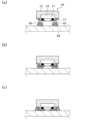
特許文献1に記載の技術について図9を用いて説明する。図9中、(a)は半導体パッケージに用いるリードフレームの外部機器と接続する側からみた図、(b)は(a)のリードフレームを用いて組み立てた半導体パッケージにおける(a)のA-A断面図、(c)は(b)の半導体パッケージの外部接続用端子を外部機器に半田接続した状態を示す図、(d)は(a)のリードフレームにおける外部接続用端子となる端子部を示すB-B断面図である。
Prior to the description of the embodiments, the circumstances leading to the derivation of the present invention and the effects of the present invention will be described.
First, the inventor of the present invention examined and considered the technique described in
The technology described in
図9(a)に示す半導体パッケージに用いるリードフレームは、リードフレームにおけるリードの裏面側の外部接続用端子となる端子部51の切断位置(図9(a)における一点鎖線上の位置)に、リードを横断する溝51bがFe-Ni合金やCu合金等の金属板からなるリードフレームに対してエッチング加工やプレス加工を施すことによって形成されている。なお、図9(a)中、52は半導体素子を搭載するパッド部、53はリードを支持するサポートバー、60は半導体素子である。
そして、リードフレームのパッド部52に半導体素子60を搭載し、リードにおける半導体素子60搭載側の内部接続端子となる端子部と半導体素子60とをボンディングワイヤ61で接続し、半導体素子搭載側を封止樹脂70で封止した状態の半導体パッケージを切断位置に沿って切断することによって、図9(b)に示すように、個々に切断された半導体パッケージの裏面に露出するリードの外部接続用端子51に、端縁部にかけて空間部51aが設けられる。
このように形成された半導体パッケージは、図9(c)に示すように、外部機器80の端子81に半田接続した状態では、半田90は外部接続用端子51の裏面から端縁部にかけて形成されている空間部51aに介在する。このため、半導体パッケージの側面に露出した外部接続用端子51の半田接続部分を目視確認でき、半導体パッケージの外部機器80との半田接続状態の良・不良を目視検査できる。
In the lead frame used for the semiconductor package shown in FIG. 9(a), at the cutting position (position on the dashed line in FIG. 9(a)) of the
Then, the
As shown in FIG. 9(c), the semiconductor package formed in this manner is soldered to
ところで、特許文献1に記載の技術では、半田接続部分を目視可能にするためのリードを横断する溝51bをFe-Ni合金やCu合金等の金属板からなるリードフレームに対してエッチング加工やプレス加工を施すことにより形成している。
しかし、特許文献1に記載の技術のように、リードフレームにおけるリードの裏面側の外部接続用端子51となる端子部の切断位置に、リードを横断する溝51bを形成すると、半導体パッケージの組立てにおける樹脂封止の際に、端子部の溝51bに樹脂が入り込み、半田接続部分を目視可能にするための空間部51aが形成されない虞がある。
即ち、リードフレームにおけるリードの裏面側の外部接続用端子となる端子部51にリードを横断する溝51bを形成すると、外部接続用端子となる端子部51は、切断位置において、図9(d)に示すようにリードの幅方向が全体にわたり薄肉状に形成される。一般に、リードフレームの半導体素子搭載側を樹脂封止する際には、リードフレームの裏面の溝に樹脂が入り込まないようにするためにリードフレームの裏面には、シート状のテープを貼り付ける。しかし、リードの幅方向に沿う溝51bの外側部分にはシート状のテープと密着する面が存在しないため、リードの幅方向に沿う溝51bの外側部分はシート状のテープから離れてしまう。ここで、シート状のテープを溝51bの面に密着させようとしても、シート状のテープが大きく変形することになり、溝51bに完全に密着させることが難しく、シート状のテープと溝51bの面とに隙間が生じ易い。その結果、樹脂封止する際にシート状のテープと溝51bの面との隙間から樹脂が回り込んで、端子部51の溝51bに樹脂が入り込み、半田接続部分を目視検査可能にするための空間部が形成されず、半導体パッケージ製品の歩留まりが悪くなる虞がある。
By the way, in the technique described in
However, as in the technique described in
That is, when a
次に、特許文献2に記載の技術も、パターン形成された金属板からなるリードフレームに対してプレス加工を施すことにより、半田接続部分を目視可能にするためスルーホールやスリットを形成する前段階の凹部を形成しているが、金属板を除去して裏面側に露出しためっき層が外部接続用端子となる端子部を構成するタイプの半導体装置を製造するための半導体素子搭載用基板の場合、めっき層に対してプレス加工を施すことにより、凹部を形成することは非常に難しい。
また、樹脂封止後に、ブレードを用いてハーフカットとフルカットの2回の切断工程が必要となり、生産効率が悪く、コストが増大してしまう。しかも、外部接続用端子が横方向へ突出するため、半導体パッケージ製品を小型化し難い。
Next, the technique described in Patent Document 2 is also a pre-stage in which through holes and slits are formed in order to make the solder connection portions visible by performing press working on a lead frame made of a patterned metal plate. In the case of a semiconductor element mounting substrate for manufacturing a semiconductor device of the type in which the metal plate is removed and the plated layer exposed on the back side constitutes the terminal portion that will be the terminal for external connection. It is very difficult to form recesses by pressing the plated layer.
In addition, after resin encapsulation, it is necessary to perform two cutting processes, half-cutting and full-cutting, using a blade, resulting in poor production efficiency and an increase in cost. Moreover, since the external connection terminals protrude in the lateral direction, it is difficult to miniaturize the semiconductor package product.
ここで、本件発明者は、特許文献1に記載の技術を改良し、リードフレームにおけるリードの裏面側の外部接続用端子となる端子部の切断位置に、凹部を形成することを着想した。そして、外部接続用端子となる端子部の切断位置に凹部を形成したリードフレームを用いて、半導体素子を搭載し樹脂で封止後に切断して、個々の半導体パッケージを製造した際に、半導体パッケージの側面に露出している外部接続用端子の端縁部が門形状に形成され、門形状の端縁部に囲まれた領域から半田付け部分を目視確認できるようにすることについて検討を行った。
Here, the inventor of the present invention improved the technique described in
図10は本発明を導出する前段階において本件発明者が検討した、側面に露出する少なくとも一部の外部接続用端子の幅が異なる半導体パッケージに用いられるリードフレームの構成を示す説明図で、(a)は外部機器と接続する側からみた図、(b)は(a)のリードフレームにおける外部接続用端子となる端子部を示すC-C断面図である。
図10のリードフレームでは、夫々の外部接続用端子となる端子部71には、ダムバー73近傍の個々のリードフレームに切断するための切断領域の内側に及ぶ所定位置に、外部接続用端子となる端子部71の幅(図10(a)において、破線の位置で切断されることによって露出する領域の幅)に応じて形成された所定形状の開口を有する凹部71b’が形成されている。
凹部71b’は、周囲を外部接続用端子となる端子部71及びダムバー73に囲まれている。そして、図10(a)において、破線の位置で切断されることによって半導体パッケージの側面に露出する外部接続用端子71の断面形状(即ち、外部接続用端子71の端縁部71a’の端面形状)は、図10(b)に示すように、門形状に形成されるようになっている。
FIG. 10 is an explanatory diagram showing the configuration of a lead frame used in a semiconductor package in which at least some of the external connection terminals exposed on the side face are different in width, which was studied by the present inventor in the stage prior to deriving the present invention. FIG. 1(a) is a view from the side connected to an external device, and (b) is a cross-sectional view taken along the line CC showing a terminal portion serving as an external connection terminal in the lead frame of (a).
In the lead frame of FIG. 10, the
The
図10に示すリードフレームは、図9に示したリードフレームとは異なり、凹部71b’の周囲を外部接続用端子となる端子部71又はダムバー73を構成する金属材料が囲んでおり、凹部71b’の周囲を囲む金属材料の面は平坦となっている。
このため、凹部71b’の周囲の金属材料の面を、シート状のテープに密着させることができ、リードフレームの半導体素子搭載側を樹脂封止する際に、樹脂の凹部71b’への入り込みを防止することができる。
In the lead frame shown in FIG. 10, unlike the lead frame shown in FIG. 9, the periphery of the
Therefore, the surface of the metal material around the
しかし、本件発明者が、更に検討を重ねたところ、リードの裏面側の外部接続端子部の切断位置に、凹部を形成した構成のリードフレームには、半導体パッケージを製造後に個片化するための切断により金属屑が凹部に付着してしまう問題があることが判明した。 However, as a result of further investigation by the inventors of the present invention, it has been found that a lead frame having a configuration in which recesses are formed at the cut positions of the external connection terminal portions on the back side of the leads is used for singulating semiconductor packages after manufacturing. It was found that there was a problem that metal scraps adhered to the concave portion due to cutting.
そこで、本件発明者は、半導体素子が搭載された領域を封止樹脂で封止した樹脂封止体から金属板を除去することによって製造され、裏面側に露出するめっき層からなる外部接続用端子がプリント基板等の外部機器と接続されるタイプの半導体パッケージの製造に用いる半導体素子搭載用基板について検討した。そして、試行錯誤の末、金属板に凹部を設けることによって柱状突起部を金属板に形成し、柱状突起部の側面および上面と凹部の底面における柱状突起部の周囲の所定領域をめっき層で覆い、金属板を除去した時に、めっき層の断面が門形状になるようにした構成の半導体素子搭載用基板を導出した。 Therefore, the inventors of the present invention have proposed an external connection terminal made of a plating layer exposed on the back side, which is manufactured by removing a metal plate from a resin sealing body in which a region where a semiconductor element is mounted is sealed with a sealing resin. A substrate for mounting a semiconductor device used in the manufacture of a semiconductor package that is connected to an external device such as a printed circuit board was investigated. After trial and error, the columnar protrusions are formed in the metal plate by providing the recesses in the metal plate, and the side and top surfaces of the columnar protrusions and the predetermined areas around the columnar protrusions on the bottom surface of the recesses are covered with a plating layer. , a substrate for mounting a semiconductor element having a configuration in which the cross section of the plating layer becomes gate-shaped when the metal plate is removed was derived.
図11~図13は本発明を導出する前段階において本件発明者が導出した、半導体素子搭載用基板の要部構成を示す説明図で、夫々の図において(a)は端子部の構造を示す断面図、(b)は(a)の半導体素子搭載用基板が多列配列された多列型半導体素子搭載用基板を示す上面図である。 11 to 13 are explanatory diagrams showing the main structure of a substrate for mounting a semiconductor device derived by the present inventor in the previous stage of deriving the present invention, and in each figure (a) shows the structure of the terminal portion. FIG. 3B is a cross-sectional view, and FIG. 4B is a top view showing a multi-row type semiconductor device mounting substrate in which the semiconductor device mounting substrates of FIG. 4A are arranged in multiple rows;
図11~図13の半導体素子搭載用基板1は、金属板10に凹部10aを設けることによって形成された柱状突起部10bの側面および上面と凹部10aの底面における柱状突起部10bの周囲の所定領域をめっき層12(図13の半導体素子搭載用基板ではめっき層12-2)が覆っている。図13中、12-1は凹部10aの底面における半導体素子搭載領域に形成されためっき層である。
柱状突起部10bは、半導体パッケージ領域の内側で四方の縁部から中央に向かって細長状に延びている。
これらの半導体素子搭載用基板1によれば、金属板10を溶解除去することで、柱状突起部10bの上面及び側面を覆うように形成しためっき層12、12-2の断面が門形状になるようにした構成にすることができる。
11 to 13, the
The
According to these semiconductor
さらに、本件発明者が、試行錯誤を重ねたところ、半田接続部分を目視し易くするためには、めっき層からなる外部接続端子の門形状の内側部分の高さ(めっき層で形成された凹部の深さ)を0.10mm以上にする必要があることが判明した。 Further, the inventors of the present invention repeated trial and error and found that the height of the gate-shaped inner portion of the external connection terminal made of the plating layer (the concave portion formed of the plating layer depth) of 0.10 mm or more.
そこで、本件発明者は、柱状突起部の高さを0.10mm以上にした構成を備えた半導体素子搭載用基板を製造し、更に、試行錯誤を重ねた。
その結果、柱状突起部の高さを0.10mm以上にした構成を備えた半導体素子搭載用基板の製造する場合、レジストフィルムを金属板に圧着することによって、外部接続端子用のめっき層を形成するためのめっき用レジストマスクを形成すると、レジストフィルムが柱状突起部の高さに追従できず、レジストフィルムと柱状突起部が形成された金属板との間に気泡が残り、レジストフィルムを圧着後に形成したレジストマスクの開口部からめっき層を形成した際に、めっき層の被膜にボイド不良を生じ易く、歩留まりが悪化し、生産性が低下することが判明した。
Therefore, the inventor of the present invention manufactured a substrate for mounting a semiconductor element having a columnar projection with a height of 0.10 mm or more, and repeated trial and error.
As a result, when manufacturing a substrate for mounting a semiconductor element having a structure in which the height of the columnar protrusion is 0.10 mm or more, the plating layer for the external connection terminal is formed by crimping the resist film onto the metal plate. When a resist mask for plating is formed for plating, the resist film cannot follow the height of the columnar protrusions, and air bubbles remain between the resist film and the metal plate on which the columnar protrusions are formed. It has been found that when the plating layer is formed from the opening of the formed resist mask, void defects are likely to occur in the film of the plating layer, resulting in deterioration of yield and productivity.
図14は本発明を導出する前段階において本件発明者が導出した、半導体素子搭載用基板の製造工程におけるめっき用レジストマスク形成のためのレジストフィルムを金属板に圧着する際の搬送状態を示す説明図で、(a)は側面図、(b)は上面図、(c)は金属板の搬送方向と、レジストフィルムが金属板に圧着される際の空気の逃げる方向を模式的に示す上面図、(d)はレジストフィルムを金属板に圧着したときの状態を模式的に示す拡大図である。
一般に、半導体装置用基板の製造工程におけるめっき加工は、図14(a)、図14(b)に示すように、搬送装置を介して金属板がライン搬送された状態で行われる。
めっき加工では、めっき用レジストマスクを形成するために、ロールに巻かれたレジストフィルムRを、搬送されてくる柱状突起部10bを備えた金属板10にローラー100を介して圧着する。このとき、レジストフィルムRと金属板10との間の空気が、金属板の搬送方向X1とは反対側の方向に逃げていく。
ここで、図14(c)に示すように、柱状突起部10bの辺が金属板の搬送方向に対し垂直に延びていると、レジストフィルムを圧着するときに、搬送方向とは反対側の方向に逃げようとする空気が、柱状突起部10bの長辺に当接して逃げにくくなる。
FIG. 14 is an explanation derived by the inventor of the present invention in a stage prior to deriving the present invention, showing a conveying state when a resist film for forming a resist mask for plating is pressure-bonded to a metal plate in the manufacturing process of a substrate for mounting a semiconductor device. In the figure, (a) is a side view, (b) is a top view, and (c) is a top view schematically showing the conveying direction of the metal plate and the direction in which air escapes when the resist film is pressure-bonded to the metal plate. and (d) is an enlarged view schematically showing a state in which the resist film is pressure-bonded to the metal plate.
Generally, the plating process in the manufacturing process of substrates for semiconductor devices is carried out in a state in which a metal plate is transported in a line via a transport device, as shown in FIGS. 14(a) and 14(b).
In the plating process, a resist film R wound into a roll is press-bonded to the transported
Here, as shown in FIG. 14(c), if the sides of the
そして、本件発明者が試行錯誤を繰り返したところ、柱状突起部10bの高さを0.10mm以上にした場合、レジストフィルムRを圧着するときに、レジストフィルムRが柱状突起部10bの高さに追従できず、金属板の搬送方向とは反対側の方向に逃げようとする空気が柱状突起部10bの辺(特に長辺)に留まった状態で、レジストフィルムRと柱状突起部10bが形成された金属板10との間に、図14(d)に示すように、気泡99が残り易くなることが判明した。
そして、このように金属板10との間で気泡99が残存する状態のレジストフィルムRにおける柱状突起部10bを囲む所定領域にめっき加工用の開口部を形成し、開口部を形成したレジストフィルムRをめっき用レジストマスクとして用いてめっき層を形成したところ、開口部近傍の気泡が残存する部位に、形成されためっき層にボイドが形成され易く、製造された半導体素子搭載用基板の歩留まりが悪化することが判明した。
As a result of repeated trial and error, the inventors of the present invention found that when the height of the
Then, an opening for plating is formed in a predetermined region surrounding the
従って、本件発明者が導出した図11~図13に示すような半導体素子搭載用基板を製造する場合、めっき用レジストマスク12、12-1、12-2の形成のためのレジストフィルムを金属板10に圧着する際に、レジストフィルムと金属板との間の空気を残存させないようにする必要がある。
しかし、図11~図13に示す半導体素子搭載用基板は、柱状突起部10bが、半導体パッケージ領域の内側で四方の縁部から中央に向かって細長状に延びた構成となっており、柱状突起部10bのいずれかの辺は、金属板10の搬送方向に対し垂直に延びている状態となるため、レジストフィルムを金属板10に圧着する際に、空気を金属板の搬送方向とは反対側の方向に完全に逃がすことが難しい。
Therefore, when manufacturing a substrate for mounting a semiconductor element as shown in FIGS. It is necessary to prevent air from remaining between the resist film and the metal plate when press-bonding to 10 .
However, in the substrate for mounting a semiconductor element shown in FIGS. 11 to 13, the
ここで、めっき用レジストマスクの形成のために、レジストフィルムを用いずに、液体状のレジストを金属板に塗布し、乾燥させることで被膜を形成するようにすれば、空気が残存する問題は生じないが、液体状のレジストはフィルム状のレジストに比べてコスト高となってしまう。 Here, in order to form a resist mask for plating, if a liquid resist is applied to a metal plate and dried to form a film without using a resist film, the problem of remaining air can be eliminated. Although it does not occur, the cost of the liquid resist is higher than that of the film resist.
そこで、本件発明者は、半導体素子が搭載された領域を封止樹脂で封止した樹脂封止体から金属板を除去することによって製造され、裏面側に露出するめっき層からなる外部接続用端子がプリント基板等の外部機器と接続されるタイプの半導体パッケージの製造に用いる半導体素子搭載用基板であって、半導体パッケージ製品の歩留まりや、生産効率を向上させ、小型化にも対応でき、しかも、半田接続部分を目視可能にする半導体素子搭載用基板の製造方法において、めっき用レジストマスクの形成のためにレジストフィルムを用いてコストを抑えながら、外部接続用端子をなすめっき層の被膜のボイド不良を防止し、半導体素子搭載用基板の歩留まりや、生産性を向上させることの可能な半導体素子搭載用基板の製造方法を導出するに至った。 Therefore, the inventors of the present invention have proposed an external connection terminal made of a plating layer exposed on the back side, which is manufactured by removing a metal plate from a resin sealing body in which a region where a semiconductor element is mounted is sealed with a sealing resin. is a substrate for mounting a semiconductor element used in the manufacture of a semiconductor package of a type that is connected to an external device such as a printed circuit board, which can improve the yield and production efficiency of semiconductor package products, and can respond to miniaturization. In a method for manufacturing a substrate for mounting a semiconductor element in which a solder connection part is visible, a void defect in a film of a plating layer that forms an external connection terminal while suppressing costs by using a resist film for forming a resist mask for plating. Thus, a method of manufacturing a semiconductor device mounting substrate capable of preventing the above and improving the yield and productivity of the semiconductor device mounting substrate has been derived.
本発明の一態様による半導体素子搭載用基板の製造方法は、複数の半導体素子搭載用基板が多列配置され、個々の半導体素子搭載用基板が、金属板の一方の側の面に凹部を設けることによって形成され、半導体パッケージ領域の内側で四方の縁部から中央に向かって細長状に延びた、0.10mm以上0.18mm以下の高さの複数の柱状突起部と、夫々の柱状突起部の側面および上面と凹部の底面における柱状突起部の周囲の所定領域を覆う、めっき層からなる複数の端子部と、を有する半導体素子搭載用基板の製造方法であって、金属板の一方の側の面上に、凹部に対応する領域を開口する開口部を有し、複数の柱状突起部に対応する領域を覆うエッチング用レジストマスクを形成するとともに、金属板の他方の側の面上に、全面を覆うエッチング用レジストマスクを形成する工程と、個々の前記柱状突起部の近傍、且つ、半導体パッケージ領域の外側の所定部位に対応する領域を開口する開口部を有し、その他の領域を覆う遮蔽部材を、金属板の一方の側に形成されているエッチング用レジストマスクから所定間隔をあけて配置した状態で、金属板の一方の面にエッチング加工を施し、0.10mm以上0.18mm以下の深さの凹部を設けることによって個々の柱状突起部を形成するとともに、所定の柱状突起部の近傍、且つ、半導体パッケージ領域の外側に位置する所定部位に対応する領域に貫通孔を形成する工程と、遮蔽部材を除去するとともにエッチング用レジストマスクを除去する工程と、搬送装置を用いて搬送される、金属板の一方の側の面上に、レジストフィルムを圧着し、夫々の柱状突起部を囲む所定領域を開口する複数の開口部を有し、その他の領域を覆うめっき用レジストマスクを形成する工程と、めっき用レジストマスクの開口部から露出する、柱状突起部の側面および上面と凹部の底面における柱状突起部の周囲の所定領域にめっき加工を施し、端子部を形成する工程と、めっき用レジストマスクを除去する工程と、を有する。 In a method for manufacturing a semiconductor element mounting substrate according to one aspect of the present invention, a plurality of semiconductor element mounting substrates are arranged in multiple rows, and each semiconductor element mounting substrate is provided with a concave portion on one side surface of a metal plate. a plurality of pillar-shaped projections having a height of 0.10 mm or more and 0.18 mm or less elongated from the four edges toward the center inside the semiconductor package region; and a plurality of terminal portions made of a plating layer covering predetermined regions around the columnar protrusions on the side and top surfaces of the recess and the bottom surface of the recess, the method comprising one side of the metal plate On the surface of the metal plate, an etching resist mask is formed that has openings that open regions corresponding to the recesses and covers regions corresponding to the plurality of columnar projections, and on the other side of the metal plate, a step of forming an etching resist mask covering the entire surface; having openings for opening regions corresponding to predetermined portions near the individual pillar-shaped protrusions and outside the semiconductor package region, and covering other regions; One surface of the metal plate is etched with the shielding member placed at a predetermined distance from the etching resist mask formed on one side of the metal plate to obtain a thickness of 0.10 mm or more and 0.18 mm or less. a step of forming individual columnar protrusions by providing recesses having a depth of 100 mm and forming through holes in areas corresponding to predetermined portions located near predetermined columnar protrusions and outside the semiconductor package area. a step of removing the shielding member and the etching resist mask; and pressing a resist film onto one side surface of the metal plate conveyed by the conveying device to form each columnar protrusion. a step of forming a plating resist mask having a plurality of openings that open a predetermined region surrounding it and covering other regions; The method includes a step of plating a predetermined region around the columnar protrusion on the bottom surface to form a terminal portion, and a step of removing the plating resist mask.
また、本発明の他の態様による半導体素子搭載用基板の製造方法は、複数の半導体素子搭載用基板が多列配置され、個々の半導体素子搭載用基板が、金属板の一方の側の面に凹部を設けることによって形成され、半導体パッケージ領域の内側で四方の縁部から中央に向かって細長状に延びた、0.10mm以上0.18mm以下の高さの複数の柱状突起部と、夫々の柱状突起部の側面および上面と凹部の底面における柱状突起部の周囲の所定領域を覆う、めっき層からなる複数の端子部と、を有する半導体素子搭載用基板の製造方法であって、金属板の一方の側の面上に、凹部に対応する領域を開口する開口部を有し、複数の柱状突起部に対応する領域を覆うエッチング用レジストマスクを形成するとともに、金属板の他方の側の面上に、個々の柱状突起部の近傍、且つ、半導体パッケージ領域の外側の所定部位に対応する領域を開口する開口部を有し、その他の領域を覆うエッチング用レジストマスクを形成する工程と、金属板の両面にエッチング加工を施し、0.10mm以上0.18mm以下の深さの凹部を設けることによって個々の柱状突起部を形成するとともに、所定の柱状突起部の近傍、且つ、半導体パッケージ領域の外側に位置する所定部位に対応する領域に貫通孔を形成する工程と、エッチング用レジストマスクを除去する工程と、搬送装置を用いて搬送される、金属板の一方の側の面上に、レジストフィルムを圧着し、夫々の柱状突起部を囲む所定領域を開口する複数の開口部を有し、その他の領域を覆うめっき用レジストマスクを形成する工程と、めっき用レジストマスクの開口部から露出する、柱状突起部の側面および上面と凹部の底面における柱状突起部の周囲の所定領域にめっき加工を施し、端子部を形成する工程と、めっき用レジストマスクを除去する工程と、を有する。 In a method for manufacturing a semiconductor element mounting substrate according to another aspect of the present invention, a plurality of semiconductor element mounting substrates are arranged in multiple rows, and each semiconductor element mounting substrate is disposed on one side surface of a metal plate. a plurality of columnar protrusions having a height of 0.10 mm or more and 0.18 mm or less formed by providing recesses and elongated from four edges toward the center inside the semiconductor package region; A method for manufacturing a substrate for mounting a semiconductor element, comprising: a plurality of terminal portions made of a plating layer covering the side surfaces and top surfaces of the columnar protrusions; An etching resist mask is formed on one surface of the metal plate so as to have openings for opening regions corresponding to the recesses and to cover regions corresponding to the plurality of columnar protrusions, and the other surface of the metal plate. a step of forming an etching resist mask on the top, having openings for opening regions corresponding to predetermined portions near the individual columnar protrusions and outside the semiconductor package region, and covering other regions; Etching is performed on both sides of the plate to form recesses with a depth of 0.10 mm or more and 0.18 mm or less, thereby forming individual columnar projections, and in the vicinity of the predetermined columnar projections and in the semiconductor package area. a step of forming a through hole in a region corresponding to a predetermined portion located outside ; a step of removing the resist mask for etching ; A step of forming a plating resist mask by pressing a resist film and having a plurality of openings opening predetermined regions surrounding the respective columnar projections and covering other regions, and exposing from the openings of the plating resist mask. a step of plating a predetermined region around the columnar projection on the side surface and top surface of the columnar projection and the bottom surface of the recess to form a terminal portion; and a step of removing the plating resist mask.
本発明の半導体素子搭載用基板の製造方法のように、金属板に対してエッチング加工を施し、0.10mm以上0.18mm以下の深さの凹部を設けることによって個々の柱状突起部を形成するとともに、個々の柱状突起部の近傍、且つ、半導体パッケージ領域の外側に位置する所定部位に対応する領域に貫通孔を形成すると、その後のめっき用レジストマスクの形成のために、搬送装置を用いて搬送される、金属板の一方の側の面上に、レジストフィルムを圧着させるときに、金属板の搬送方向に対し垂直に延びている柱状突起部の長辺に、当たって逃げ難くなっている空気を、貫通孔を介して金属板の下方へ逃がし易くなる。そして、レジストフィルムと柱状突起部が形成された金属板との間の気泡の発生が防止でき、めっき用レジストマスクの形成のためのレジストフィルムを柱状突起部の高さに追従した状態で圧着させることができる。その結果、このレジストフィルムにめっき加工用の開口部を形成してめっき層を形成したとき、形成されためっき層にボイドが形成されず、製造された半導体素子搭載用基板の歩留まりや、生産性が向上する。 As in the method of manufacturing a substrate for mounting a semiconductor element of the present invention, a metal plate is subjected to an etching process to form recesses having a depth of 0.10 mm or more and 0.18 mm or less, thereby forming individual columnar projections. At the same time, when the through-holes are formed in the vicinity of the individual columnar protrusions and in the regions corresponding to the predetermined portions located outside the semiconductor package region, the conveying device is used for the subsequent formation of the plating resist mask. When the resist film is crimped onto one side surface of the conveyed metal plate, it hits the long sides of the columnar protrusions extending perpendicularly to the conveying direction of the metal plate, making it difficult to escape. Air can easily escape downward from the metal plate through the through holes. Then, the generation of air bubbles between the resist film and the metal plate on which the columnar projections are formed can be prevented, and the resist film for forming the resist mask for plating is crimped while following the height of the columnar projections. be able to. As a result, when an opening for plating is formed in this resist film to form a plating layer, voids are not formed in the formed plating layer, and the yield and productivity of the manufactured substrate for mounting a semiconductor element are improved. improves.
本発明の半導体素子搭載用基板の製造方法においては、好ましくは、貫通孔を形成する工程において、貫通孔を、0.03mm以上0.12mm以下の径を有するように形成する。
貫通孔をこの範囲の径に形成すれば、搬送装置を用いて搬送される、金属板の一方の側の面上に、レジストフィルムを圧着させるときに、金属板の搬送方向に対し垂直に延びている柱状突起部の長辺に、当たって逃げ難くなっている空気を、貫通孔を介して金属板の下方へ確実に逃がすことができる。
In the method of manufacturing a substrate for mounting a semiconductor element of the present invention, preferably, in the step of forming the through hole, the through hole is formed to have a diameter of 0.03 mm or more and 0.12 mm or less.
By forming the through-hole with a diameter within this range, when the resist film is crimped onto one side of the metal plate conveyed by the conveying device, the resist film extends perpendicularly to the conveying direction of the metal plate. The air that hits the long side of the columnar protrusion and is difficult to escape can be reliably released below the metal plate through the through hole.
また、本発明の半導体素子搭載用基板の製造方法においては、好ましくは、貫通孔を形成する工程において、貫通孔を、長手方向が金属板の搬送方向に対して垂直となる、柱状突起部の近傍、且つ、半導体パッケージ領域の外側に位置する所定部位に対応する領域に形成する。
貫通孔をこのような領域に形成すれば、搬送装置を用いて搬送される、金属板の一方の側の面上に、レジストフィルムを圧着させるときに、金属板の搬送方向に対し垂直に延びている柱状突起部の長辺に、当たって逃げ難くなっている空気を、貫通孔を介して金属板の下方へ確実に逃がすことができ、且つ、貫通孔の形成箇所を必要最小限に抑えることができる。
In the method of manufacturing a substrate for mounting a semiconductor element of the present invention, preferably, in the step of forming the through-hole, the through-hole is formed as a columnar protrusion whose longitudinal direction is perpendicular to the conveying direction of the metal plate. It is formed in a region corresponding to a predetermined portion located near and outside the semiconductor package region.
If the through-hole is formed in such a region, when the resist film is crimped onto one side of the metal plate conveyed by the conveying device, the through-hole extends perpendicularly to the conveying direction of the metal plate. The air that hits the long side of the columnar protrusion that is in contact with and is difficult to escape can be reliably released below the metal plate through the through-hole, and the number of through-hole formation locations is minimized. be able to.
従って、本発明によれば、半導体素子が搭載された領域を封止樹脂で封止した樹脂封止体から金属板を除去することによって製造され、裏面側に露出するめっき層からなる外部接続用端子がプリント基板等の外部機器と接続されるタイプの半導体パッケージの製造に用いる半導体素子搭載用基板であって、半導体パッケージ製品の歩留まりや、生産効率を向上させ、小型化にも対応でき、しかも、半田接続部分を目視可能にする半導体素子搭載用基板の製造方法において、コストを抑えながら、外部接続用端子をなすめっき層の被膜のボイド不良を防止し、半導体素子搭載用基板の歩留まりや、生産性を向上させることの可能な半導体素子搭載用基板の製造方法が得られる。 Therefore, according to the present invention, the semiconductor device for external connection is manufactured by removing the metal plate from the resin sealing body in which the region where the semiconductor element is mounted is sealed with the sealing resin, and is made of the plating layer exposed on the back side. A substrate for mounting a semiconductor element used in the manufacture of a semiconductor package whose terminals are connected to an external device such as a printed circuit board, which improves the yield and production efficiency of the semiconductor package product, and can also respond to miniaturization. In a method for manufacturing a semiconductor element mounting board in which a solder connection part is visible, void defects in a film of a plating layer forming an external connection terminal are prevented while suppressing costs, thereby increasing the yield of the semiconductor element mounting board, A method for manufacturing a substrate for mounting a semiconductor element that can improve productivity is obtained.
以下、図面を参照して、本発明を実施するための形態の説明を行うこととする。 Hereinafter, with reference to the drawings, description will be given of a mode for carrying out the present invention.
図1は本発明の一実施形態に係る半導体素子搭載用基板の製造方法によって製造された半導体素子搭載用基板の要部構成の一例を示す説明図で、(a)は端子部の構造を示す横断面図、(b)は(a)の半導体素子搭載用基板が多列配列された多列型半導体素子搭載用基板の一例を示す上面図、(c)は(b)の部分縦断面図である。図2は図1(a)、図1(b)の半導体素子搭載用基板における隣り合う半導体パッケージ領域の端子部同士の配置態様の他の例を示す図で、(a)は断面図、(b)は(a)の半導体素子搭載用基板が多列配列された多列型半導体素子搭載用基板の上面図、(c)は(b)の部分縦断面図である。図3は本発明の一実施形態に係る半導体素子搭載用基板の製造方法によって製造された他のタイプの半導体素子搭載用基板の要部構成の一例を示す説明図で、(a)は端子部の構造を示す断面図、(b)は(a)の半導体素子搭載用基板が多列配列された多列型半導体素子搭載用基板の一例を示す上面図、(c)は(b)の部分縦断面図である。 FIG. 1 is an explanatory view showing an example of the configuration of a main part of a semiconductor device mounting substrate manufactured by a method for manufacturing a semiconductor device mounting substrate according to one embodiment of the present invention, and (a) shows the structure of a terminal portion. (b) is a top view showing an example of a multi-row type semiconductor device mounting substrate in which the semiconductor device mounting substrates of (a) are arranged in multiple rows; (c) is a partial longitudinal sectional view of (b). is. FIGS. 2A and 2B are diagrams showing another example of arrangement of terminal portions of adjacent semiconductor package regions in the substrate for mounting a semiconductor device shown in FIGS. b) is a top view of a multi-row type semiconductor element mounting substrate in which the semiconductor element mounting substrates of (a) are arranged in multiple rows, and (c) is a partial longitudinal sectional view of (b). FIG. 3 is an explanatory diagram showing an example of the main configuration of another type of semiconductor device mounting substrate manufactured by the method for manufacturing a semiconductor device mounting substrate according to one embodiment of the present invention, in which (a) is a terminal portion. (b) is a top view showing an example of a multi-row semiconductor device mounting substrate in which the semiconductor device mounting substrates of (a) are arranged in multiple rows; (c) is the part (b) It is a longitudinal cross-sectional view.
本実施形態の半導体素子搭載用基板の製造方法によって製造された半導体素子搭載用基板1は、例えば、図1(a)に示すように、凹部10aと、複数の柱状突起部10bと、複数の端子部12を有し、図1(b)に示すように、多列配列されている。
凹部10aは、金属板10の一方の側の面に形成されており、0.10mm以上0.18mm以下の深さを有している。
柱状突起部10bは、金属板10に凹部10aを設けることによって形成され、半導体パッケージ領域(図1(b)において一点鎖線で囲まれた矩形状の領域)の内側で四方の縁部から中央に向かって細長状に延びている。
端子部12は、柱状突起部10bの側面および上面と凹部10aの底面における柱状突起部10bの周囲の所定領域を覆うように形成された、めっき層で構成されている。
また、金属板10には、図1(b)、図1(c)に示すように、個々の柱状突起部10bの近傍、且つ、半導体パッケージ領域の外側の所定部位に対応する領域に貫通孔18が形成されている。貫通孔18は、0.03mm以上0.12mm以下の径を有している。
そして、複数の端子部12は、半田等の接続部材を介して、端子部12の下段又は端子部12の上段に、半導体素子をフリップチップ実装することができるようになっている(図示省略)。
なお、本実施形態の半導体素子搭載用基板1は、図1(a)、図1(b)の例では、隣り合う半導体パッケージ領域(不図示)の柱状突起部10b同士が接続した態様に配置されているが、図2(a)、図2(b)に示すように、隣り合う半導体パッケージ領域(不図示)の柱状突起部10b同士が離れた態様に配置されたものであってもよい。
また、本実施形態の半導体素子搭載用基板1は、図3(a)、図3(b)に示すように、凹部10aの底面の中央部にめっき層で形成されたパッド部12-1と、パッド部12-1の周辺であって、凹部10aを設けることによって形成された柱状突起部10bの側面および上面と凹部10aの底面における柱状突起部10bの周囲の所定領域を覆うように形成されためっき層で構成された複数の端子部12-2を有し、パッド部12-1に半導体素子を搭載するとともに、ボンディングワイヤ等の接続部材を介して。端子部12-2の上面と半導体素子の電極とをワイヤボンディングできるようにしたものであってもよい。
A semiconductor
The
The
The
1(b) and 1(c), the
The plurality of
In the example of FIGS. 1A and 1B, the
Further, as shown in FIGS. 3A and 3B, the
次に、図1(a)~図1(c)のように構成される本実施形態の半導体素子搭載用基板1の製造工程の一例を、図4を用いて説明する。なお、図4において(a)~(i)は、図1(a)と同じ側からみたときの状態を示し、(a’)~(i’)は図1(c)と同じ側からみたときの状態を示している。また、製造の各工程において実施される、薬液洗浄や水洗洗浄を含む前処理・後処理等は、便宜上説明を省略する。
まず、銅または銅合金の金属板10を半導体素子搭載用基板材料として準備する(図4(a)、図4(a’)参照)。
次に、金属板10にハーフエッチング加工を施して柱状突起部10bと貫通孔18を形成する。詳しくは、金属板10の両面にドライフィルムレジスト等の第1のレジスト層R1を形成する(図4(b)、図4(b’)参照)。次いで、図1(a)、図1(b)に示した柱状突起部10bに対応する所定のパターンが描画されたガラスマスクを用いて、金属板10の一方の側の第1のレジスト層R1を露光するとともに、金属板10の他方の側の第1のレジスト層R1を全面にわたって露光し、露光後に夫々の第1のレジスト層R1を現像する。そして、金属板10の一方の側の面上に、柱状突起部10bに対応する領域を覆い、凹部10aに対応する領域が開口したエッチング用レジストマスク31を形成するとともに、金属板10の他方の側の面上に、全面を覆うエッチング用レジストマスク31を形成する(図4(c)、図4(c’)参照)。次いで、個々の柱状突起部10bの近傍、且つ、半導体パッケージ領域の外側の所定部位に対応する領域(図1に示す貫通孔18に対応する領域)を開口する開口部を有し、その他の領域を覆う遮蔽部材35を、金属板10の一方の側に形成されているエッチング用レジストマスク31から所定間隔をあけて配置した状態で、金属板10の一方の側からハーフエッチング加工を施し、0.10mm以上0.18mm以下の深さの凹部10aを設けることによって個々の柱状突起部10bを形成するとともに、柱状突起部10bの近傍、且つ、半導体パッケージ領域の外側に位置する所定部位に対応する領域に貫通孔18を形成する(図4(d)、図4(d’)参照)。次いで、金属板10の両面上に形成したエッチング用レジストマスク31を除去する(図4(e)、図4(e’)参照)。
Next, an example of a manufacturing process of the
First, a copper or copper
Next, the
次に、金属板10の一方の側における、柱状突起部10bの側面および上面と凹部10aの底面における柱状突起部10bの周囲の所定領域を覆うめっき層からなる複数の端子部12を形成する。詳しくは、金属板10の両面に、ドライフィルムレジストからなる第2のレジスト層R2を圧着する(図4(f)、図4(f’)参照)。このとき、金属板10の搬送方向に対し垂直に延びている柱状突起部10bの長辺に、当たって逃げ難くなっていた空気が、貫通孔18を介して金属板10の下方へ逃げていく。なお、第2のレジストR2の圧着に際しては、予め、金属板10の一方の側(即ち、柱状突起部10bが形成されている側)の面に圧着する第2のレジスト層を、金属板10の他方の側の面に圧着する第2のレジスト層よりも僅かに早く圧着するようにローラー等の圧着手段(不図示)を配置しておく。次いで、図1(a)、図1(b)に示した端子部12に対応する所定のパターンが描画されたガラスマスクを用いて、金属板10の一方の側の第2のレジスト層R2を露光し、露光後に第2のレジスト層R2を現像する。そして、金属板10の一方の側の面上に、柱状突起部10bの側面および上面と凹部10aの底面における柱状突起部10bの周囲の所定領域を覆う端子部12に対応する領域に複数の開口部を有するめっき用レジストマスク32を形成する(図4(g)、図4(g’)参照)。次いで、めっき用レジストマスク32の開口部に、例えば、Au、Pd、Ni、Pdの順でめっき加工を施し、複数の端子部12を形成する(図4(h)、図4(h’)参照)。
なお、めっき層の表面は、粗化処理を施すのが良い。めっき層の表面を粗化処理する場合、例えば、めっき層の形成をNiめっきで終えて、Niめっき層を粗化めっきで形成しても良い。また、例えば、平滑なNiめっき層を形成した後に、Niめっき層の表面をエッチングにて粗化処理しても良い。また、例えば、めっき層の形成をCuめっきで終えて、Cuめっき層の表面を陽極酸化処理又はエッチングにて粗化処理してもよい。さらに、例えば、粗化めっき層形成後に、順に、Pd/Auめっき層を積層してもよい。
次いで、金属板10の両面上に形成しためっき用レジストマスク32を除去する(図4(i)、図4(i’)参照)。
これにより、本実施形態の半導体素子搭載用基板1が出来上がる。
Next, on one side of the
The surface of the plated layer is preferably roughened. When roughening the surface of the plated layer, for example, the formation of the plated layer may be finished with Ni plating, and the Ni plated layer may be formed with roughening plating. Further, for example, after forming a smooth Ni plating layer, the surface of the Ni plating layer may be roughened by etching. Alternatively, for example, the formation of the plating layer may be finished with Cu plating, and the surface of the Cu plating layer may be roughened by anodizing or etching. Further, for example, after forming the roughening plating layer, Pd/Au plating layers may be sequentially laminated.
Next, the plating resist
Thereby, the
なお、図1(a)~図1(c)のように構成される本実施形態の半導体素子搭載用基板1の製造工程は、図4に示した例に限られるものではなく、例えば、図5に示す例のようなものであってもよい。
なお、図5において(a)~(i)は、図1(a)と同じ側からみたときの状態を示し、(a’)~(i’)は図1(c)と同じ側からみたときの状態を示している。また、製造の各工程において実施される、薬液洗浄や水洗洗浄を含む前処理・後処理等は、便宜上説明を省略する。
図5に示す例の半導体素子搭載用基板1の製造工程では、金属板10にハーフエッチング加工を施して柱状突起部10bと貫通孔18を形成する処理手順が図4に示す例のものとは異なる。
詳しくは、金属板10の両面にドライフィルムレジスト等の第1のレジスト層R1を形成(図5(b)、図5(b’)参照)後、図1(a)、図1(b)に示した柱状突起部10bに対応する所定のパターンが描画されたガラスマスクを用いて、金属板10の一方の側の第1のレジスト層R1を露光するとともに、柱状突起部10bの近傍、且つ、半導体パッケージ領域の外側に位置する貫通孔18に対応する所定パターンが描画されたガラスマスクを用いて、金属板10の他方の側の第1のレジスト層R1を露光し、露光後に夫々の第1のレジスト層R1を現像する。そして、金属板10の一方の側の面上に、柱状突起部10bに対応する領域を覆い、凹部10aに対応する領域が開口したエッチング用レジストマスク31を形成するとともに、金属板10の他方の側の面上に、柱状突起部10bの近傍、且つ、半導体パッケージ領域の外側に位置する貫通孔18に対応する領域が開口し、それ以外の領域を覆うエッチング用レジストマスク31を形成する(図5(c)、図5(c’)参照)。次いで、金属板10の両側からハーフエッチング加工を施し、一方の側に0.10mm以上0.18mm以下の深さの凹部10aを設けることによって個々の柱状突起部10bを形成するとともに、柱状突起部10bの近傍、且つ、半導体パッケージ領域の外側に位置する所定部位に対応する領域に貫通孔18を形成する(図5(d)、図5(d’)参照)。
その他の製造手順は、図4に示した例と略同様である(図5(e)~図5(i)、図5(e’)~図5(i’)参照)。
1(a) to 1(c) is not limited to the example shown in FIG. 5 may be used.
5, (a) to (i) show the state when viewed from the same side as FIG. 1 (a), and (a') to (i') show the state when viewed from the same side as FIG. 1 (c). indicates the state of the moment. Further, for the sake of convenience, descriptions of pre-treatments and post-treatments including cleaning with chemicals and cleaning with water, which are carried out in each process of manufacturing, are omitted.
In the manufacturing process of the
Specifically, after forming a first resist layer R1 such as a dry film resist on both surfaces of the metal plate 10 (see FIGS. 5(b) and 5(b')), The first resist layer R1 on one side of the
Other manufacturing procedures are substantially the same as the example shown in FIG. 4 (see FIGS. 5(e) to 5(i) and 5(e') to 5(i')).
次に、本実施形態の半導体素子搭載用基板の製造方法によって製造された半導体素子搭載用基板1を用いた半導体パッケージの製造手順を、図6を用いて説明する。
まず、端子部12の表面の内部端子接続部に半田17等を介して半導体素子20をフリップチップ接続する(図6(a)参照)。
次に、図示しないモールド金型をセットし、半導体素子搭載側を封止樹脂15で封止する(図6(b)参照)。
次に、金属板10を除去し(図6(c)参照)、所定の半導体パッケージの寸法に切断する(図6(d)参照)。これにより、本実施形態の半導体素子搭載用基板1を用いた半導体パッケージ40が完成する(図6(e)参照)。
Next, a procedure for manufacturing a semiconductor package using the semiconductor
First, the
Next, a molding die (not shown) is set, and the semiconductor element mounting side is sealed with a sealing resin 15 (see FIG. 6(b)).
Next, the
本実施形態の半導体素子搭載用基板の製造方法によれば、金属板10に対してエッチング加工を施し、0.10mm以上0.18mm以下の深さの凹部10aを設けることによって個々の柱状突起部10bを形成するとともに、個々の柱状突起部10bの近傍、且つ、半導体パッケージ領域の外側に位置する所定部位に対応する領域に貫通孔18を形成するようにしたので、その後のめっき用レジストマスク32の形成のために、搬送装置を用いて搬送される、金属板10の一方の側の面上に、レジストフィルム(第2のレジスト層R2)を圧着させるときに、金属板10の搬送方向に対し垂直に延びている柱状突起部10bの長辺に、当たって逃げ難くなっている空気を、貫通孔18を介して金属板10の下方へ逃がし易くなる。そして、レジストフィルム(第2のレジスト層R2)と柱状突起部10bが形成された金属板10との間の気泡の発生が防止でき、めっき用レジストマスク32の形成のためのレジストフィルム(第2のレジスト層R2)を柱状突起部10bの高さに追従した状態で圧着させることができる。その結果、このレジストフィルムにめっき加工用の開口部を形成してめっき層12を形成したとき、形成されためっき層12にボイドが形成されず、製造された半導体素子搭載用基板の歩留まり、生産性が向上する。
According to the manufacturing method of the substrate for mounting a semiconductor element of the present embodiment, the
また、本実施形態の半導体素子搭載用基板の製造方法によれば、貫通孔18を、0.03mm以上0.12mm以下の径を有するように形成したので、搬送装置を用いて搬送される、金属板10の一方の側の面上に、レジストフィルム(第2のレジスト層R2)を圧着させるときに、金属板10の搬送方向に対し垂直に延びている柱状突起部10bの長辺に、当たって逃げ難くなっている空気を、貫通孔18を介して金属板の下方へ確実に逃がすことができる。
Further, according to the manufacturing method of the substrate for mounting a semiconductor element of the present embodiment, the through
また、本実施形態の半導体素子搭載用基板の製造方法において、貫通孔18を、長手方向が金属板10の搬送方向に対して垂直となる、柱状突起部10bの近傍、且つ、半導体パッケージ領域の外側に位置する所定部位に対応する領域に形成するようにすれば、搬送装置を用いて搬送される、金属板10の一方の側の面上に、レジストフィルム(第2のレジスト層R2)を圧着させるときに、金属板10の搬送方向に対し垂直に延びている柱状突起部10bの長辺に、当たって逃げ難くなっている空気を、貫通孔18を介して金属板の下方へ確実に逃がすことができ、且つ、貫通孔18の形成箇所を必要最小限に抑えることができる。
In addition, in the method of manufacturing a substrate for mounting a semiconductor element according to the present embodiment, the through
従って、本実施形態によれば、半導体素子が搭載された領域を封止樹脂で封止した樹脂封止体から金属板を除去することによって製造され、裏面側に露出するめっき層からなる外部接続用端子がプリント基板等の外部機器と接続されるタイプの半導体パッケージの製造に用いる半導体素子搭載用基板であって、半導体パッケージ製品の歩留まりや、生産効率を向上させ、小型化にも対応でき、しかも、半田接続部分を目視可能にする半導体素子搭載用基板の製造方法において、コストを抑えながら、外部接続用端子をなすめっき層の被膜のボイド不良を防止し、半導体素子搭載用基板の歩留まりや、生産性を向上させることの可能な半導体素子搭載用基板の製造方法が得られる。 Therefore, according to the present embodiment, the external connection is manufactured by removing the metal plate from the resin sealing body in which the region where the semiconductor element is mounted is sealed with the sealing resin, and is made of the plating layer exposed on the back side. A substrate for mounting a semiconductor element used in the manufacture of a semiconductor package whose terminals are connected to an external device such as a printed circuit board. Moreover, in the manufacturing method of the semiconductor element mounting board in which the solder connection portion is made visible, void defects in the film of the plating layer forming the external connection terminal are prevented while suppressing the cost, and the yield of the semiconductor element mounting board is improved. , a method for manufacturing a substrate for mounting a semiconductor element capable of improving productivity is obtained.
次に、本発明の半導体素子搭載用基板の製造方法の実施例を説明する。
実施例1
まず、金属板10として、厚さ0.20mmの銅系材料を準備し(図4(a)、図4(a’)参照)、両面に、第1のレジスト層R1としてドライフィルムレジストを圧着した(図4(b)、図4(b’)参照)。
Next, an embodiment of the method for manufacturing a substrate for mounting a semiconductor element according to the present invention will be described.
Example 1
First, a copper-based material having a thickness of 0.20 mm is prepared as the metal plate 10 (see FIGS. 4(a) and 4(a')), and a dry film resist is crimped on both sides as a first resist layer R1. (See FIGS. 4(b) and 4(b')).
次に、図1(a)、図1(b)に示した柱状突起部10bに対応する所定のパターンが描画されたガラスマスクを用いて、金属板10の一方の側の第1のレジスト層R1を露光するとともに、金属板10の他方の側の第1のレジスト層R1を全面にわたって露光し、露光後に夫々の第1のレジスト層R1を現像して、金属板10の一方の側の面上に、柱状突起部10bに対応する領域を覆い、凹部10aに対応する領域が開口したエッチング用レジストマスク31を形成するとともに、金属板10の他方の側の面上に、全面を覆うエッチング用レジストマスク31を形成した(図4(c)、図4(c’)参照)。
次に、個々の柱状突起部10bの近傍、且つ、半導体パッケージ領域の外側の所定部位に対応する領域(図1に示す貫通孔18に対応する領域)を開口する開口部を有し、その他の領域を覆う遮蔽部材35を、金属板10の一方の側に形成されているエッチング用レジストマスク31から所定間隔をあけて配置した状態で、金属板10の一方の側から深さ0.15mmのハーフエッチング加工を施し、金属板におけるハーフエッチング加工を施した深さにおいて凹部10aを設けることによって個々の柱状突起部10bを形成するとともに、柱状突起部10bの近傍、且つ、半導体パッケージ領域の外側に位置する所定部位に対応する領域に0.10mmの径の貫通孔18を形成した(図4(d)、図4(d’)参照)。なお、エッチング液は、塩化第二鉄液を使用した。
次に、金属板10の両面上に形成したエッチング用レジストマスク31を剥離した(図4(e)、図4(e’)参照)。
Next, using a glass mask on which a predetermined pattern corresponding to the
Next, there is an opening that opens a region (region corresponding to the through
Next, the etching resist
次に、金属板10の両面に、第2のレジスト層R2としてドライフィルムレジストを圧着した(図4(f)、図4(f’)参照)。このとき、金属板10の搬送方向に対し垂直に延びている柱状突起部10bの長辺に、当たって逃げ難くなっている空気を、貫通孔18を介して金属板10の下方へ逃がすようにした。
次に、図1(a)、図1(b)に示した端子部12に対応する所定のパターンが描画されたガラスマスクを用いて、金属板10の一方の側の第2のレジスト層R2を露光し、露光後に第2のレジスト層R2を現像して、金属板10の一方の側の面上に、柱状突起部10bの側面および上面と凹部10aの底面における柱状突起部10bの周囲の所定領域を覆う端子部12に対応する領域に複数の開口部を有するめっき用レジストマスク32を形成した(図4(g)、図4(g’)参照)。
次に、めっき用レジストマスク32の開口部に、Auを0.01μm、Pdを0.03μm、Niを30.0μm、Pdを0.03μmの厚さで順次めっき加工を施し、複数の端子部12を形成した(図4(h)、図4(h’)参照)。
次に、金属板10の両面上に形成しためっき用レジストマスク32を剥離し(図4(i)、図4(i’)参照)、実施例1の半導体素子搭載用基板1を得た。
Next, a dry film resist was pressure-bonded as a second resist layer R2 to both surfaces of the metal plate 10 (see FIGS. 4(f) and 4(f')). At this time, the air that hits the long sides of the
Next, a second resist layer R2 on one side of the
Next, the openings of the plating resist
Next, the plating resist
次に、実施例1の半導体素子搭載用基板1における端子部12の表面の内部端子接続部に半田17等を介して半導体素子20をフリップチップ接続し(図6(a)参照)、図示しないモールド金型をセットし、半導体素子搭載側を封止樹脂15で封止した(図6(b)参照)。
次に、金属板10を除去した(図6(c)参照)。
Next, the
Next, the
このとき、金属板10を除去した封止樹脂体における半導体素子搭載側とは反対側の面(裏面)が凸形状に形成され、凸形状に形成された封止樹脂体の面から外部接続用端子となる端子部12を構成するめっき層が露出した状態に仕上がった。
次に、所定の半導体パッケージの寸法に切断した(図6(d)参照)。これにより、実施例1の半導体素子搭載用基板1を用いた半導体パッケージ40を得た(図6(e)参照)。
次に、実施例1の半導体素子搭載用基板1を用いた半導体パッケージ40の外部接続用端子を外部機器であるプリント基板80の端子に半田接続して、プリント基板80に装着した。このとき、リフローにより溶けた半田90が、端子部12の裏面の外部接続用端子部の段差が形成されることによって設けられた空間部に濡れ広がり、半導体パッケージ40の側面に露出した外部接続用端子12の半田接続部分を目視確認でき、半導体パッケージ40の外部機器であるプリント基板80との半田接続状態の良・不良を目視検査できる状態となった(図7(a)~図7(c)参照)。
At this time, the surface (rear surface) of the sealing resin body from which the
Next, it was cut into a predetermined semiconductor package size (see FIG. 6(d)). Thus, a
Next, the external connection terminals of the
比較例1
比較例1では、実施例1におけるハーフエッチング加工に際し、個々の柱状突起部10bの近傍、且つ、半導体パッケージ領域の外側の所定部位に対応する領域(図1に示す貫通孔18に対応する領域)を開口する開口部を有し、その他の領域を覆う遮蔽部材35を用いた貫通孔18の形成を行わず、0.15mmの深さの凹部10aを設けることによって個々の柱状突起部10bのみを形成し、それ以外は、実施例1と略同様の条件及び手順で、半導体素子搭載用基板を製造した。
より詳しくは、金属板10の両面に第1のレジスト層として、ドライフィルムレジストを圧着し、図11(a)、図11(b)に示した柱状突起部10bに対応する所定のパターンが描画されたガラスマスクを用いて、金属板10の一方の側の第1のレジスト層を露光するとともに、金属板10の他方の側の第1のレジスト層を全面にわたって露光し、露光後に夫々の第1のレジスト層を現像して、金属板10の一方の側の面上に、図11(a)、図11(b)に示した柱状突起部10bに対応する領域を覆い、凹部10aに対応する領域が開口したエッチング用レジストマスクを形成するとともに、金属板10の他方の側の面上に、全面を覆うエッチング用レジストマスクを形成した。次に、金属板10の一方の側からハーフエッチング加工を施し、0.15mmの深さの凹部10aを設けることによって個々の柱状突起部10bを形成した。次にエッチング用レジストマスクを剥離し、金属板10の両面に、ドライフィルムレジストからなる第2のレジスト層を圧着した。次に、図11(a)、図11(b)に示した端子部12に対応する所定のパターンが描画されたガラスマスクを用いて、金属板10の一方の側の第2のレジスト層を露光し、露光後に第2のレジスト層を現像して、金属板10の一方の側の面上に、柱状突起部10bの側面および上面と凹部の底面における柱状突起部10bの周囲の所定領域を覆う図11(a)、図11(b)に示した端子部12に対応する領域に複数の開口部を有するめっき用レジストマスクを形成した。
次に、めっき用レジストマスクの開口部に、Auを0.01μm、Pdを0.03μm、Niを30.0μm、Pdを0.03μmの厚さで順次めっき加工を施し、複数の端子部12を形成した。
次に、金属板10の両面上に形成したレジストマスクを剥離し、比較例1の半導体素子搭載用基板を得た。
Comparative example 1
In Comparative Example 1, during the half-etching process in Example 1, a region (a region corresponding to the through
More specifically, a dry film resist is pressure-bonded as a first resist layer to both surfaces of the
Next, the openings of the plating resist mask are sequentially plated with 0.01 μm Au, 0.03 μm Pd, 30.0 μm Ni, and 0.03 μm Pd to form a plurality of
Next, the resist masks formed on both surfaces of the
次に、実施例1と同様、比較例1の半導体素子搭載用基板における端子部の表面の内部端子接続部に半田等を介して半導体素子をフリップチップ接続し、図示しないモールド金型をセットし、半導体素子搭載側を封止樹脂で封止し、その後、金属板を除去した。
このとき、金属板を除去した封止樹脂体における半導体素子搭載側とは反対側の面が平坦に形成され、平坦に形成された封止樹脂体の面から外部接続用端子となる端子部を構成するめっき層が露出した状態に仕上がった。
次に、所定の半導体パッケージの寸法に切断した。これにより、比較例1の半導体素子搭載用基板を用いた半導体パッケージを得た。
次に、比較例1の半導体素子搭載用基板を用いた半導体パッケージの外部接続用端子を外部機器であるプリント基板の端子に半田接続して、プリント基板に装着した。
Next, as in Example 1, the semiconductor element was flip-chip connected to the internal terminal connection portion on the surface of the terminal portion of the semiconductor element mounting substrate of Comparative Example 1 via solder or the like, and a molding die (not shown) was set. , the semiconductor element mounting side was sealed with a sealing resin, and then the metal plate was removed.
At this time, the surface of the encapsulating resin body from which the metal plate has been removed is formed flat on the side opposite to the side on which the semiconductor element is mounted, and the terminal portions to be the external connection terminals are formed from the flatly formed surface of the encapsulating resin body. It was finished in a state in which the constituting plating layer was exposed.
Next, it was cut into a predetermined size of a semiconductor package. Thus, a semiconductor package using the substrate for mounting a semiconductor element of Comparative Example 1 was obtained.
Next, the external connection terminals of the semiconductor package using the semiconductor element mounting substrate of Comparative Example 1 were connected by soldering to the terminals of the printed circuit board as an external device, and mounted on the printed circuit board.
外部機器接続後の半田接続状態の外観観察のし易さの評価
実施例1及び比較例1の夫々の半導体素子搭載用基板を用いて製造した、夫々の半導体パッケージを、半田を介して外部機器であるプリント基板の端子へ接続後の半田接続状態の外観観察のし易さを評価した。
実施例1、比較例1の夫々の半導体素子搭載用基板1を用いて製造した、夫々の半導体パッケージ40を外部機器であるプリント基板80の端子へ接続した場合、半導体パッケージ40の側面に全ての端子部12の外部機器側の面と外部機器であるプリント基板80の端子との間に半田が充填されていることを、半導体パッケージ40の側面に露出しためっき層からなる外部接続用端子の端縁部の側から目視で確認することができた。
Evaluation of easiness of appearance observation of solder connection state after connection to external equipment The ease of external observation of the solder connection state after connection to the terminal of the printed circuit board was evaluated.
When each
半導体素子搭載用基板における端子部をなすめっき層の被膜形状評価
実施例1、比較例1の夫々の製造方法を用いて1ブロック当たり縦4個、横4個に配列された半導体素子搭載用基板を作製し、夫々作製した半導体素子搭載用基板を用いて製造した、各1000個の半導体パッケージの外部接続用端子を外観検査した。詳しくは、夫々作製した半搭載素子搭載用基板における端子部を形成するめっき層における、ボイド発生を原因とする、めっき層を形成する範囲外への漏れ出しが発生した半導体素子搭載用基板の個数を調べた。
なお、めっき層の漏れ出しの発生の有無検査は、20倍の光学顕微鏡装置を備えた外観検査装置を用いて行った。
Film shape evaluation of the plating layer forming the terminal portion of the semiconductor device mounting substrate Semiconductor device mounting substrates arranged in 4 vertical and 4 horizontal blocks per block using the respective manufacturing methods of Example 1 and Comparative Example 1 , and external connection terminals of 1,000 semiconductor packages manufactured using the semiconductor element mounting substrates thus manufactured were visually inspected. Specifically, the number of semi-mounted device mounting substrates in which leaking outside the range of forming the plating layer due to the occurrence of voids in the plating layer forming the terminal part of each manufactured semi-mounted device mounting substrate occurs. examined.
The presence or absence of leakage of the plating layer was checked using a visual inspection apparatus equipped with a 20x optical microscope.
その結果、比較例1の製造方法を用いて製造した多列型半導体素子搭載用基板においては、1000個の半導体素子搭載用基板中、365個の半導体素子搭載用基板の端子部を形成するめっき層の漏れ出しが発生した。
これに対し、実施例1の製造方法を用いて製造した多列型半導体素子搭載用基板においては、1000個の半導体素子搭載用基板中、端子部を形成するめっき層の漏れ出しが発生した半導体素子搭載用基板は、0個であった。
As a result, in the multi-row type semiconductor element mounting substrates manufactured using the manufacturing method of Comparative Example 1, 365 out of 1000 semiconductor element mounting substrates were plated for forming the terminal portions of the semiconductor element mounting substrates. Layer leakage occurred.
On the other hand, in the multi-row type semiconductor element mounting substrates manufactured using the manufacturing method of Example 1, among the 1,000 semiconductor element mounting substrates, the plating layer forming the terminal portion leaked out. The number of device mounting substrates was zero.
以上、本発明の好ましい実施形態及び実施例について詳説したが、本発明は、上述した実施形態及び実施例に制限されることはなく、本発明の範囲を逸脱することなく、上述した実施形態及び実施例に種々の変形及び置換を加えることができる。
例えば、柱状突起部10bとともに貫通孔18を形成する手法として、図4(d)、図4(d’)に示した、個々の柱状突起部10bの近傍、且つ、半導体パッケージ領域の外側の所定部位に対応する領域(図1に示す貫通孔18に対応する領域)を開口する開口部を有し、その他の領域を覆う遮蔽部材35を、金属板10の一方の側に形成されているエッチング用レジストマスク31から所定間隔をあけた配置と、図5(c)、図5(c’)に示した、金属板10の他方の側の面上に、柱状突起部10bの近傍、且つ、半導体パッケージ領域の外側に位置する所定部位(貫通孔18)に対応する領域が開口し、それ以外の領域を覆うように形成されたエッチング用レジストマスク31と、を併用して、金属板10の両側からエッチング加工を行うようにしてもよい。
Although the preferred embodiments and examples of the present invention have been described in detail above, the present invention is not limited to the above-described embodiments and examples, and can be modified without departing from the scope of the present invention. Various modifications and substitutions can be made to the examples.
For example, as a method of forming the through-
また、例えば、本発明の実施形態及び実施例の半導体素子搭載用基板の製造方法によって製造される、半導体素子搭載用基板において、貫通孔18は、所定の柱状端子部の近傍、且つ、半導体パッケージ領域の外側に位置する所定部位として、図6(d)に示したような所定寸法の半導体パッケージに切断する範囲内であれば、どのような配置形態であってもよい。
例えば、貫通孔18は、図1(b)、図2(b)、図3(b)に示したような、夫々の柱状端子部を覆うめっき層を形成する範囲の間の位置の他に、例えば、図8(a)~図8(e)に示すような位置に設けても良い。詳しくは、個々の柱状端子部を覆うめっき層を形成する範囲の端部の辺に対応した位置(図8(a)、図8(c)参照)や、隣り合う柱状端子部を覆うめっき層を形成する範囲の端部の角部に対応する位置(図8(b)参照)や、複数の柱状端子部を覆うめっき層を形成する範囲の端部の辺をまたぐ位置(図8(d)、図8(e)参照)に設けても良い。また、貫通孔18は、丸穴でもスリット状の長穴でもよい。そして、図8(a)~図8(e)に示した貫通孔18の配置態様は、図1~図3に示したいずれのタイプの半導体素子搭載用基板においても適用可能である。
Further, for example, in the semiconductor element mounting board manufactured by the method for manufacturing a semiconductor element mounting board according to the embodiments and examples of the present invention, the through
For example, the through-
本発明の半導体素子搭載用基板の製造方法は、端子部がめっき層で形成され、裏面側に露出する端子部裏面の外部接続用端子がプリント基板等と接続されるタイプの半導体パッケージに用いられることが求められる分野に有用である。 The method for manufacturing a substrate for mounting a semiconductor element according to the present invention is used for a semiconductor package of a type in which a terminal portion is formed of a plating layer, and external connection terminals on the back surface of the terminal portion exposed on the back side are connected to a printed circuit board or the like. It is useful in fields where this is required.
1 半導体素子搭載用基板
10 金属板
10a 凹部
10b 柱状突起部
12 端子部(めっき層)
15 封止樹脂
17 半田
18 貫通孔
20、60 半導体素子
21、70 封止樹脂
31 エッチング用レジストマスク
32 めっき用レジストマスク
40 半導体パッケージ
51 端子部(外部接続用端子)
51a 空間部
51b 溝
52 パッド部
53 サポートバー
61 ボンディングワイヤ
71 端子部
71a’ 端縁部
71b’ 凹部
73 ダムバー
80 外部機器(プリント基板)
81 端子
90 半田
99 金属板とレジストフィルムとの間で残存する気泡(空気)
100 ローラー
R レジストフィルム
R1 第1のレジスト層
R2 第2のレジスト層
REFERENCE SIGNS
15 sealing resin
17
81
100 roller R resist film R1 first resist layer R2 second resist layer
Claims (4)
前記金属板の一方の側の面上に、前記凹部に対応する領域を開口する開口部を有し、複数の前記柱状突起部に対応する領域を覆うエッチング用レジストマスクを形成するとともに、前記金属板の他方の側の面上に、全面を覆うエッチング用レジストマスクを形成する工程と、
個々の前記柱状突起部の近傍、且つ、前記半導体パッケージ領域の外側の所定部位に対応する領域を開口する開口部を有し、その他の領域を覆う遮蔽部材を、前記金属板の一方の側に形成されている前記エッチング用レジストマスクから所定間隔をあけて配置した状態で、前記金属板の一方の面にエッチング加工を施し、0.10mm以上0.18mm以下の深さの前記凹部を設けることによって個々の前記柱状突起部を形成するとともに、所定の前記柱状突起部の近傍、且つ、前記半導体パッケージ領域の外側に位置する所定部位に対応する領域に貫通孔を形成する工程と、
前記遮蔽部材を除去するとともに前記エッチング用レジストマスクを除去する工程と、
搬送装置を用いて搬送される、前記金属板の一方の側の面上に、レジストフィルムを圧着し、夫々の前記柱状突起部を囲む所定領域を開口する複数の開口部を有し、その他の領域を覆うめっき用レジストマスクを形成する工程と、
前記めっき用レジストマスクの開口部から露出する、前記柱状突起部の側面および上面と前記凹部の底面における前記柱状突起部の周囲の所定領域にめっき加工を施し、前記端子部を形成する工程と、
前記めっき用レジストマスクを除去する工程と、
を有することを特徴とする半導体素子搭載用基板の製造方法。 A plurality of semiconductor element mounting substrates are arranged in multiple rows, and each semiconductor element mounting substrate is formed by providing a concave portion on one side surface of a metal plate, and is formed from four edges inside the semiconductor package region. a plurality of columnar protrusions with a height of 0.10 mm or more and 0.18 mm or less elongated toward the center; A method of manufacturing a substrate for mounting a semiconductor element, comprising:
forming, on one surface of the metal plate, an etching resist mask having openings for opening regions corresponding to the recesses and covering regions corresponding to the plurality of columnar protrusions; forming an etching resist mask covering the entire surface on the other side of the plate;
A shielding member having openings for opening regions corresponding to predetermined portions near the individual columnar projections and outside the semiconductor package region and covering other regions is provided on one side of the metal plate. Etching is performed on one surface of the metal plate while the metal plate is arranged at a predetermined distance from the formed etching resist mask to form the recess having a depth of 0.10 mm or more and 0.18 mm or less. forming the individual columnar protrusions by forming through holes in regions corresponding to predetermined portions located near predetermined columnar protrusions and outside the semiconductor package region;
removing the shielding member and removing the etching resist mask;
A resist film is crimped onto one side surface of the metal plate, which is conveyed using a conveying device, and has a plurality of openings that open predetermined regions surrounding the respective columnar projections, and other openings. forming a plating resist mask covering the region;
a step of plating a predetermined region around the columnar projection on the side surface and upper surface of the columnar projection and the bottom surface of the recess exposed from the opening of the resist mask for plating to form the terminal portion;
a step of removing the resist mask for plating;
A method for manufacturing a substrate for mounting a semiconductor device, comprising:
前記金属板の一方の側の面上に、前記凹部に対応する領域を開口する開口部を有し、複数の前記柱状突起部に対応する領域を覆うエッチング用レジストマスクを形成するとともに、前記金属板の他方の側の面上に、個々の前記柱状突起部の近傍、且つ、前記半導体パッケージ領域の外側の所定部位に対応する領域を開口する開口部を有し、その他の領域を覆うエッチング用レジストマスクを形成する工程と、
前記金属板の両面にエッチング加工を施し、0.10mm以上0.18mm以下の深さの前記凹部を設けることによって個々の前記柱状突起部を形成するとともに、所定の前記柱状突起部の近傍、且つ、前記半導体パッケージ領域の外側に位置する所定部位に対応する領域に貫通孔を形成する工程と、
前記エッチング用レジストマスクを除去する工程と、
搬送装置を用いて搬送される、前記金属板の一方の側の面上に、レジストフィルムを圧着し、夫々の前記柱状突起部を囲む所定領域を開口する複数の開口部を有し、その他の領域を覆うめっき用レジストマスクを形成する工程と、
前記めっき用レジストマスクの開口部から露出する、前記柱状突起部の側面および上面と前記凹部の底面における前記柱状突起部の周囲の所定領域にめっき加工を施し、前記端子部を形成する工程と、
前記めっき用レジストマスクを除去する工程と、
を有することを特徴とする半導体素子搭載用基板の製造方法。 A plurality of semiconductor element mounting substrates are arranged in multiple rows, and each semiconductor element mounting substrate is formed by providing a concave portion on one side surface of a metal plate, and is formed from four edges inside the semiconductor package region. a plurality of columnar protrusions with a height of 0.10 mm or more and 0.18 mm or less elongated toward the center; A method of manufacturing a substrate for mounting a semiconductor element, comprising:
forming, on one surface of the metal plate, an etching resist mask having openings for opening regions corresponding to the recesses and covering regions corresponding to the plurality of columnar protrusions; On the surface of the other side of the plate, there is an opening for opening a region corresponding to a predetermined portion near each of the columnar projections and outside the semiconductor package region, and for etching to cover the other region. forming a resist mask;
Etching is performed on both sides of the metal plate to form the individual columnar projections by providing the recesses with a depth of 0.10 mm or more and 0.18 mm or less, and near the predetermined columnar projections, and forming a through hole in a region corresponding to a predetermined portion located outside the semiconductor package region;
removing the etching resist mask;
A resist film is crimped onto one side surface of the metal plate, which is conveyed using a conveying device, and has a plurality of openings that open predetermined regions surrounding the respective columnar projections, and other openings. forming a plating resist mask covering the region;
a step of plating a predetermined region around the columnar projection on the side surface and upper surface of the columnar projection and the bottom surface of the recess exposed from the opening of the resist mask for plating to form the terminal portion;
a step of removing the resist mask for plating;
A method for manufacturing a substrate for mounting a semiconductor device, comprising:
Priority Applications (1)
| Application Number | Priority Date | Filing Date | Title |
|---|---|---|---|
| JP2019070791A JP7260372B2 (en) | 2019-04-02 | 2019-04-02 | Method for manufacturing substrate for mounting semiconductor device |
Applications Claiming Priority (1)
| Application Number | Priority Date | Filing Date | Title |
|---|---|---|---|
| JP2019070791A JP7260372B2 (en) | 2019-04-02 | 2019-04-02 | Method for manufacturing substrate for mounting semiconductor device |
Publications (2)
| Publication Number | Publication Date |
|---|---|
| JP2020170775A JP2020170775A (en) | 2020-10-15 |
| JP7260372B2 true JP7260372B2 (en) | 2023-04-18 |
Family
ID=72746385
Family Applications (1)
| Application Number | Title | Priority Date | Filing Date |
|---|---|---|---|
| JP2019070791A Active JP7260372B2 (en) | 2019-04-02 | 2019-04-02 | Method for manufacturing substrate for mounting semiconductor device |
Country Status (1)
| Country | Link |
|---|---|
| JP (1) | JP7260372B2 (en) |
Citations (3)
| Publication number | Priority date | Publication date | Assignee | Title |
|---|---|---|---|---|
| JP2017157644A (en) | 2016-02-29 | 2017-09-07 | Shマテリアル株式会社 | Lead frame for multi-row type LED |
| JP2018046218A (en) | 2016-09-16 | 2018-03-22 | 新光電気工業株式会社 | Lead frame, manufacturing method for the same, and electronic component device |
| JP2019021815A (en) | 2017-07-19 | 2019-02-07 | 大口マテリアル株式会社 | Semiconductor element mounting substrate and manufacturing method thereof |
Family Cites Families (1)
| Publication number | Priority date | Publication date | Assignee | Title |
|---|---|---|---|---|
| JP3028160B2 (en) * | 1992-07-31 | 2000-04-04 | 株式会社三井ハイテック | Lead frame continuous manufacturing equipment |
-
2019
- 2019-04-02 JP JP2019070791A patent/JP7260372B2/en active Active
Patent Citations (3)
| Publication number | Priority date | Publication date | Assignee | Title |
|---|---|---|---|---|
| JP2017157644A (en) | 2016-02-29 | 2017-09-07 | Shマテリアル株式会社 | Lead frame for multi-row type LED |
| JP2018046218A (en) | 2016-09-16 | 2018-03-22 | 新光電気工業株式会社 | Lead frame, manufacturing method for the same, and electronic component device |
| JP2019021815A (en) | 2017-07-19 | 2019-02-07 | 大口マテリアル株式会社 | Semiconductor element mounting substrate and manufacturing method thereof |
Also Published As
| Publication number | Publication date |
|---|---|
| JP2020170775A (en) | 2020-10-15 |
Similar Documents
| Publication | Publication Date | Title |
|---|---|---|
| CN109285823B (en) | Semiconductor element mounting substrate and method for manufacturing the same | |
| TWI668826B (en) | Lead frame, semiconductor device | |
| KR102811924B1 (en) | Semiconductor package with sidewall plating | |
| TWI787343B (en) | Substrate for mounting semiconductor element and manufacturing method thereof | |
| JP6841550B2 (en) | Lead frame and its manufacturing method | |
| JP7311226B2 (en) | Lead frame | |
| TWI784400B (en) | lead frame | |
| JP7260372B2 (en) | Method for manufacturing substrate for mounting semiconductor device | |
| JP7184429B2 (en) | Method for manufacturing substrate for mounting semiconductor device | |
| TWI811617B (en) | lead frame | |
| JP6524526B2 (en) | Semiconductor element mounting substrate and semiconductor device, and methods of manufacturing the same | |
| US10312187B2 (en) | Multi-row wiring member for semiconductor device and method for manufacturing the same | |
| JP2017163106A (en) | Lead frame assembly substrate and semiconductor device assembly | |
| JP6615654B2 (en) | Semiconductor element mounting substrate, semiconductor device, semiconductor element mounting substrate manufacturing method, and semiconductor device manufacturing method | |
| JP3706082B2 (en) | Lead frame, method of manufacturing the same, and method of manufacturing semiconductor device using the lead frame | |
| TWI631671B (en) | Semiconductor element mounting substrate, semiconductor device, and manufacturing method thereof | |
| JP7004259B2 (en) | Lead frame and its manufacturing method | |
| JP2704128B2 (en) | Lead frame for semiconductor device and method of manufacturing the same | |
| JP6901201B2 (en) | Substrate for mounting semiconductor elements and its manufacturing method | |
| JP2019075483A (en) | Lead frame | |
| JP2017034094A (en) | Semiconductor element mounting substrate, semiconductor device and manufacturing method therefor | |
| TW202147537A (en) | Lead frame capable of preventing deformation due to a reduction in the strength of the lead frame | |
| JP2017216366A (en) | Wiring member for multi-row type semiconductor device and manufacturing method thereof | |
| JP2011029482A (en) | Method of manufacturing semiconductor device |
Legal Events
| Date | Code | Title | Description |
|---|---|---|---|
| A521 | Request for written amendment filed |
Free format text: JAPANESE INTERMEDIATE CODE: A523 Effective date: 20190409 |
|
| A521 | Request for written amendment filed |
Free format text: JAPANESE INTERMEDIATE CODE: A523 Effective date: 20190627 |
|
| A621 | Written request for application examination |
Free format text: JAPANESE INTERMEDIATE CODE: A621 Effective date: 20211201 |
|
| A977 | Report on retrieval |
Free format text: JAPANESE INTERMEDIATE CODE: A971007 Effective date: 20221013 |
|
| A131 | Notification of reasons for refusal |
Free format text: JAPANESE INTERMEDIATE CODE: A131 Effective date: 20221101 |
|
| A521 | Request for written amendment filed |
Free format text: JAPANESE INTERMEDIATE CODE: A523 Effective date: 20221111 |
|
| TRDD | Decision of grant or rejection written | ||
| A01 | Written decision to grant a patent or to grant a registration (utility model) |
Free format text: JAPANESE INTERMEDIATE CODE: A01 Effective date: 20230307 |
|
| A61 | First payment of annual fees (during grant procedure) |
Free format text: JAPANESE INTERMEDIATE CODE: A61 Effective date: 20230406 |
|
| R150 | Certificate of patent or registration of utility model |
Ref document number: 7260372 Country of ref document: JP Free format text: JAPANESE INTERMEDIATE CODE: R150 |
|
| S111 | Request for change of ownership or part of ownership |
Free format text: JAPANESE INTERMEDIATE CODE: R313113 |
|
| R350 | Written notification of registration of transfer |
Free format text: JAPANESE INTERMEDIATE CODE: R350 |