JP7156641B2 - Packages for semiconductor devices and semiconductor devices - Google Patents
Packages for semiconductor devices and semiconductor devices Download PDFInfo
- Publication number
- JP7156641B2 JP7156641B2 JP2019024289A JP2019024289A JP7156641B2 JP 7156641 B2 JP7156641 B2 JP 7156641B2 JP 2019024289 A JP2019024289 A JP 2019024289A JP 2019024289 A JP2019024289 A JP 2019024289A JP 7156641 B2 JP7156641 B2 JP 7156641B2
- Authority
- JP
- Japan
- Prior art keywords
- side wall
- conductive layer
- package
- bonding material
- sidewall
- Prior art date
- Legal status (The legal status is an assumption and is not a legal conclusion. Google has not performed a legal analysis and makes no representation as to the accuracy of the status listed.)
- Active
Links
Images


Classifications
-
- H—ELECTRICITY
- H01—ELECTRIC ELEMENTS
- H01L—SEMICONDUCTOR DEVICES NOT COVERED BY CLASS H10
- H01L23/00—Details of semiconductor or other solid state devices
- H01L23/48—Arrangements for conducting electric current to or from the solid state body in operation, e.g. leads, terminal arrangements ; Selection of materials therefor
- H01L23/488—Arrangements for conducting electric current to or from the solid state body in operation, e.g. leads, terminal arrangements ; Selection of materials therefor consisting of soldered or bonded constructions
- H01L23/495—Lead-frames or other flat leads
- H01L23/49517—Additional leads
-
- H—ELECTRICITY
- H01—ELECTRIC ELEMENTS
- H01L—SEMICONDUCTOR DEVICES NOT COVERED BY CLASS H10
- H01L23/00—Details of semiconductor or other solid state devices
- H01L23/12—Mountings, e.g. non-detachable insulating substrates
- H01L23/14—Mountings, e.g. non-detachable insulating substrates characterised by the material or its electrical properties
- H01L23/142—Metallic substrates having insulating layers
-
- H—ELECTRICITY
- H01—ELECTRIC ELEMENTS
- H01L—SEMICONDUCTOR DEVICES NOT COVERED BY CLASS H10
- H01L23/00—Details of semiconductor or other solid state devices
- H01L23/02—Containers; Seals
- H01L23/04—Containers; Seals characterised by the shape of the container or parts, e.g. caps, walls
- H01L23/043—Containers; Seals characterised by the shape of the container or parts, e.g. caps, walls the container being a hollow construction and having a conductive base as a mounting as well as a lead for the semiconductor body
- H01L23/047—Containers; Seals characterised by the shape of the container or parts, e.g. caps, walls the container being a hollow construction and having a conductive base as a mounting as well as a lead for the semiconductor body the other leads being parallel to the base
-
- H—ELECTRICITY
- H01—ELECTRIC ELEMENTS
- H01L—SEMICONDUCTOR DEVICES NOT COVERED BY CLASS H10
- H01L23/00—Details of semiconductor or other solid state devices
- H01L23/02—Containers; Seals
- H01L23/10—Containers; Seals characterised by the material or arrangement of seals between parts, e.g. between cap and base of the container or between leads and walls of the container
-
- H—ELECTRICITY
- H01—ELECTRIC ELEMENTS
- H01L—SEMICONDUCTOR DEVICES NOT COVERED BY CLASS H10
- H01L23/00—Details of semiconductor or other solid state devices
- H01L23/12—Mountings, e.g. non-detachable insulating substrates
-
- H—ELECTRICITY
- H01—ELECTRIC ELEMENTS
- H01L—SEMICONDUCTOR DEVICES NOT COVERED BY CLASS H10
- H01L23/00—Details of semiconductor or other solid state devices
- H01L23/48—Arrangements for conducting electric current to or from the solid state body in operation, e.g. leads, terminal arrangements ; Selection of materials therefor
- H01L23/488—Arrangements for conducting electric current to or from the solid state body in operation, e.g. leads, terminal arrangements ; Selection of materials therefor consisting of soldered or bonded constructions
- H01L23/495—Lead-frames or other flat leads
- H01L23/49579—Lead-frames or other flat leads characterised by the materials of the lead frames or layers thereon
-
- H—ELECTRICITY
- H01—ELECTRIC ELEMENTS
- H01L—SEMICONDUCTOR DEVICES NOT COVERED BY CLASS H10
- H01L2223/00—Details relating to semiconductor or other solid state devices covered by the group H01L23/00
- H01L2223/58—Structural electrical arrangements for semiconductor devices not otherwise provided for
- H01L2223/64—Impedance arrangements
- H01L2223/66—High-frequency adaptations
- H01L2223/6644—Packaging aspects of high-frequency amplifiers
- H01L2223/6655—Matching arrangements, e.g. arrangement of inductive and capacitive components
-
- H—ELECTRICITY
- H01—ELECTRIC ELEMENTS
- H01L—SEMICONDUCTOR DEVICES NOT COVERED BY CLASS H10
- H01L2224/00—Indexing scheme for arrangements for connecting or disconnecting semiconductor or solid-state bodies and methods related thereto as covered by H01L24/00
- H01L2224/01—Means for bonding being attached to, or being formed on, the surface to be connected, e.g. chip-to-package, die-attach, "first-level" interconnects; Manufacturing methods related thereto
- H01L2224/26—Layer connectors, e.g. plate connectors, solder or adhesive layers; Manufacturing methods related thereto
- H01L2224/31—Structure, shape, material or disposition of the layer connectors after the connecting process
- H01L2224/32—Structure, shape, material or disposition of the layer connectors after the connecting process of an individual layer connector
- H01L2224/321—Disposition
- H01L2224/32151—Disposition the layer connector connecting between a semiconductor or solid-state body and an item not being a semiconductor or solid-state body, e.g. chip-to-substrate, chip-to-passive
- H01L2224/32221—Disposition the layer connector connecting between a semiconductor or solid-state body and an item not being a semiconductor or solid-state body, e.g. chip-to-substrate, chip-to-passive the body and the item being stacked
- H01L2224/32245—Disposition the layer connector connecting between a semiconductor or solid-state body and an item not being a semiconductor or solid-state body, e.g. chip-to-substrate, chip-to-passive the body and the item being stacked the item being metallic
-
- H—ELECTRICITY
- H01—ELECTRIC ELEMENTS
- H01L—SEMICONDUCTOR DEVICES NOT COVERED BY CLASS H10
- H01L2224/00—Indexing scheme for arrangements for connecting or disconnecting semiconductor or solid-state bodies and methods related thereto as covered by H01L24/00
- H01L2224/01—Means for bonding being attached to, or being formed on, the surface to be connected, e.g. chip-to-package, die-attach, "first-level" interconnects; Manufacturing methods related thereto
- H01L2224/42—Wire connectors; Manufacturing methods related thereto
- H01L2224/47—Structure, shape, material or disposition of the wire connectors after the connecting process
- H01L2224/48—Structure, shape, material or disposition of the wire connectors after the connecting process of an individual wire connector
- H01L2224/4805—Shape
- H01L2224/4809—Loop shape
- H01L2224/48091—Arched
-
- H—ELECTRICITY
- H01—ELECTRIC ELEMENTS
- H01L—SEMICONDUCTOR DEVICES NOT COVERED BY CLASS H10
- H01L2224/00—Indexing scheme for arrangements for connecting or disconnecting semiconductor or solid-state bodies and methods related thereto as covered by H01L24/00
- H01L2224/01—Means for bonding being attached to, or being formed on, the surface to be connected, e.g. chip-to-package, die-attach, "first-level" interconnects; Manufacturing methods related thereto
- H01L2224/42—Wire connectors; Manufacturing methods related thereto
- H01L2224/47—Structure, shape, material or disposition of the wire connectors after the connecting process
- H01L2224/48—Structure, shape, material or disposition of the wire connectors after the connecting process of an individual wire connector
- H01L2224/481—Disposition
- H01L2224/48151—Connecting between a semiconductor or solid-state body and an item not being a semiconductor or solid-state body, e.g. chip-to-substrate, chip-to-passive
- H01L2224/48221—Connecting between a semiconductor or solid-state body and an item not being a semiconductor or solid-state body, e.g. chip-to-substrate, chip-to-passive the body and the item being stacked
- H01L2224/48245—Connecting between a semiconductor or solid-state body and an item not being a semiconductor or solid-state body, e.g. chip-to-substrate, chip-to-passive the body and the item being stacked the item being metallic
-
- H—ELECTRICITY
- H01—ELECTRIC ELEMENTS
- H01L—SEMICONDUCTOR DEVICES NOT COVERED BY CLASS H10
- H01L2224/00—Indexing scheme for arrangements for connecting or disconnecting semiconductor or solid-state bodies and methods related thereto as covered by H01L24/00
- H01L2224/01—Means for bonding being attached to, or being formed on, the surface to be connected, e.g. chip-to-package, die-attach, "first-level" interconnects; Manufacturing methods related thereto
- H01L2224/42—Wire connectors; Manufacturing methods related thereto
- H01L2224/47—Structure, shape, material or disposition of the wire connectors after the connecting process
- H01L2224/48—Structure, shape, material or disposition of the wire connectors after the connecting process of an individual wire connector
- H01L2224/484—Connecting portions
- H01L2224/48463—Connecting portions the connecting portion on the bonding area of the semiconductor or solid-state body being a ball bond
- H01L2224/48464—Connecting portions the connecting portion on the bonding area of the semiconductor or solid-state body being a ball bond the other connecting portion not on the bonding area also being a ball bond, i.e. ball-to-ball
-
- H—ELECTRICITY
- H01—ELECTRIC ELEMENTS
- H01L—SEMICONDUCTOR DEVICES NOT COVERED BY CLASS H10
- H01L2224/00—Indexing scheme for arrangements for connecting or disconnecting semiconductor or solid-state bodies and methods related thereto as covered by H01L24/00
- H01L2224/73—Means for bonding being of different types provided for in two or more of groups H01L2224/10, H01L2224/18, H01L2224/26, H01L2224/34, H01L2224/42, H01L2224/50, H01L2224/63, H01L2224/71
- H01L2224/732—Location after the connecting process
- H01L2224/73251—Location after the connecting process on different surfaces
- H01L2224/73265—Layer and wire connectors
-
- H—ELECTRICITY
- H01—ELECTRIC ELEMENTS
- H01L—SEMICONDUCTOR DEVICES NOT COVERED BY CLASS H10
- H01L2224/00—Indexing scheme for arrangements for connecting or disconnecting semiconductor or solid-state bodies and methods related thereto as covered by H01L24/00
- H01L2224/80—Methods for connecting semiconductor or other solid state bodies using means for bonding being attached to, or being formed on, the surface to be connected
- H01L2224/83—Methods for connecting semiconductor or other solid state bodies using means for bonding being attached to, or being formed on, the surface to be connected using a layer connector
- H01L2224/8338—Bonding interfaces outside the semiconductor or solid-state body
- H01L2224/83399—Material
- H01L2224/834—Material with a principal constituent of the material being a metal or a metalloid, e.g. boron [B], silicon [Si], germanium [Ge], arsenic [As], antimony [Sb], tellurium [Te] and polonium [Po], and alloys thereof
- H01L2224/83438—Material with a principal constituent of the material being a metal or a metalloid, e.g. boron [B], silicon [Si], germanium [Ge], arsenic [As], antimony [Sb], tellurium [Te] and polonium [Po], and alloys thereof the principal constituent melting at a temperature of greater than or equal to 950°C and less than 1550°C
- H01L2224/83447—Copper [Cu] as principal constituent
-
- H—ELECTRICITY
- H01—ELECTRIC ELEMENTS
- H01L—SEMICONDUCTOR DEVICES NOT COVERED BY CLASS H10
- H01L2224/00—Indexing scheme for arrangements for connecting or disconnecting semiconductor or solid-state bodies and methods related thereto as covered by H01L24/00
- H01L2224/91—Methods for connecting semiconductor or solid state bodies including different methods provided for in two or more of groups H01L2224/80 - H01L2224/90
- H01L2224/92—Specific sequence of method steps
- H01L2224/922—Connecting different surfaces of the semiconductor or solid-state body with connectors of different types
- H01L2224/9222—Sequential connecting processes
- H01L2224/92242—Sequential connecting processes the first connecting process involving a layer connector
- H01L2224/92247—Sequential connecting processes the first connecting process involving a layer connector the second connecting process involving a wire connector
-
- H—ELECTRICITY
- H01—ELECTRIC ELEMENTS
- H01L—SEMICONDUCTOR DEVICES NOT COVERED BY CLASS H10
- H01L24/00—Arrangements for connecting or disconnecting semiconductor or solid-state bodies; Methods or apparatus related thereto
- H01L24/01—Means for bonding being attached to, or being formed on, the surface to be connected, e.g. chip-to-package, die-attach, "first-level" interconnects; Manufacturing methods related thereto
- H01L24/26—Layer connectors, e.g. plate connectors, solder or adhesive layers; Manufacturing methods related thereto
- H01L24/31—Structure, shape, material or disposition of the layer connectors after the connecting process
- H01L24/32—Structure, shape, material or disposition of the layer connectors after the connecting process of an individual layer connector
-
- H—ELECTRICITY
- H01—ELECTRIC ELEMENTS
- H01L—SEMICONDUCTOR DEVICES NOT COVERED BY CLASS H10
- H01L24/00—Arrangements for connecting or disconnecting semiconductor or solid-state bodies; Methods or apparatus related thereto
- H01L24/01—Means for bonding being attached to, or being formed on, the surface to be connected, e.g. chip-to-package, die-attach, "first-level" interconnects; Manufacturing methods related thereto
- H01L24/42—Wire connectors; Manufacturing methods related thereto
- H01L24/47—Structure, shape, material or disposition of the wire connectors after the connecting process
- H01L24/48—Structure, shape, material or disposition of the wire connectors after the connecting process of an individual wire connector
-
- H—ELECTRICITY
- H01—ELECTRIC ELEMENTS
- H01L—SEMICONDUCTOR DEVICES NOT COVERED BY CLASS H10
- H01L24/00—Arrangements for connecting or disconnecting semiconductor or solid-state bodies; Methods or apparatus related thereto
- H01L24/73—Means for bonding being of different types provided for in two or more of groups H01L24/10, H01L24/18, H01L24/26, H01L24/34, H01L24/42, H01L24/50, H01L24/63, H01L24/71
-
- H—ELECTRICITY
- H01—ELECTRIC ELEMENTS
- H01L—SEMICONDUCTOR DEVICES NOT COVERED BY CLASS H10
- H01L2924/00—Indexing scheme for arrangements or methods for connecting or disconnecting semiconductor or solid-state bodies as covered by H01L24/00
- H01L2924/0001—Technical content checked by a classifier
- H01L2924/00014—Technical content checked by a classifier the subject-matter covered by the group, the symbol of which is combined with the symbol of this group, being disclosed without further technical details
-
- H—ELECTRICITY
- H01—ELECTRIC ELEMENTS
- H01L—SEMICONDUCTOR DEVICES NOT COVERED BY CLASS H10
- H01L2924/00—Indexing scheme for arrangements or methods for connecting or disconnecting semiconductor or solid-state bodies as covered by H01L24/00
- H01L2924/10—Details of semiconductor or other solid state devices to be connected
- H01L2924/102—Material of the semiconductor or solid state bodies
- H01L2924/1025—Semiconducting materials
- H01L2924/10251—Elemental semiconductors, i.e. Group IV
- H01L2924/10253—Silicon [Si]
-
- H—ELECTRICITY
- H01—ELECTRIC ELEMENTS
- H01L—SEMICONDUCTOR DEVICES NOT COVERED BY CLASS H10
- H01L2924/00—Indexing scheme for arrangements or methods for connecting or disconnecting semiconductor or solid-state bodies as covered by H01L24/00
- H01L2924/10—Details of semiconductor or other solid state devices to be connected
- H01L2924/102—Material of the semiconductor or solid state bodies
- H01L2924/1025—Semiconducting materials
- H01L2924/10251—Elemental semiconductors, i.e. Group IV
- H01L2924/10254—Diamond [C]
-
- H—ELECTRICITY
- H01—ELECTRIC ELEMENTS
- H01L—SEMICONDUCTOR DEVICES NOT COVERED BY CLASS H10
- H01L2924/00—Indexing scheme for arrangements or methods for connecting or disconnecting semiconductor or solid-state bodies as covered by H01L24/00
- H01L2924/10—Details of semiconductor or other solid state devices to be connected
- H01L2924/102—Material of the semiconductor or solid state bodies
- H01L2924/1025—Semiconducting materials
- H01L2924/1026—Compound semiconductors
- H01L2924/1027—IV
- H01L2924/10272—Silicon Carbide [SiC]
-
- H—ELECTRICITY
- H01—ELECTRIC ELEMENTS
- H01L—SEMICONDUCTOR DEVICES NOT COVERED BY CLASS H10
- H01L2924/00—Indexing scheme for arrangements or methods for connecting or disconnecting semiconductor or solid-state bodies as covered by H01L24/00
- H01L2924/10—Details of semiconductor or other solid state devices to be connected
- H01L2924/102—Material of the semiconductor or solid state bodies
- H01L2924/1025—Semiconducting materials
- H01L2924/1026—Compound semiconductors
- H01L2924/1032—III-V
- H01L2924/10329—Gallium arsenide [GaAs]
-
- H—ELECTRICITY
- H01—ELECTRIC ELEMENTS
- H01L—SEMICONDUCTOR DEVICES NOT COVERED BY CLASS H10
- H01L2924/00—Indexing scheme for arrangements or methods for connecting or disconnecting semiconductor or solid-state bodies as covered by H01L24/00
- H01L2924/10—Details of semiconductor or other solid state devices to be connected
- H01L2924/102—Material of the semiconductor or solid state bodies
- H01L2924/1025—Semiconducting materials
- H01L2924/1026—Compound semiconductors
- H01L2924/1032—III-V
- H01L2924/1033—Gallium nitride [GaN]
-
- H—ELECTRICITY
- H01—ELECTRIC ELEMENTS
- H01L—SEMICONDUCTOR DEVICES NOT COVERED BY CLASS H10
- H01L2924/00—Indexing scheme for arrangements or methods for connecting or disconnecting semiconductor or solid-state bodies as covered by H01L24/00
- H01L2924/10—Details of semiconductor or other solid state devices to be connected
- H01L2924/11—Device type
- H01L2924/13—Discrete devices, e.g. 3 terminal devices
- H01L2924/1304—Transistor
- H01L2924/1306—Field-effect transistor [FET]
- H01L2924/13064—High Electron Mobility Transistor [HEMT, HFET [heterostructure FET], MODFET]
-
- H—ELECTRICITY
- H01—ELECTRIC ELEMENTS
- H01L—SEMICONDUCTOR DEVICES NOT COVERED BY CLASS H10
- H01L2924/00—Indexing scheme for arrangements or methods for connecting or disconnecting semiconductor or solid-state bodies as covered by H01L24/00
- H01L2924/10—Details of semiconductor or other solid state devices to be connected
- H01L2924/11—Device type
- H01L2924/13—Discrete devices, e.g. 3 terminal devices
- H01L2924/1304—Transistor
- H01L2924/1306—Field-effect transistor [FET]
- H01L2924/13091—Metal-Oxide-Semiconductor Field-Effect Transistor [MOSFET]
-
- H—ELECTRICITY
- H01—ELECTRIC ELEMENTS
- H01L—SEMICONDUCTOR DEVICES NOT COVERED BY CLASS H10
- H01L2924/00—Indexing scheme for arrangements or methods for connecting or disconnecting semiconductor or solid-state bodies as covered by H01L24/00
- H01L2924/15—Details of package parts other than the semiconductor or other solid state devices to be connected
- H01L2924/171—Frame
- H01L2924/1715—Shape
Landscapes
- Engineering & Computer Science (AREA)
- Computer Hardware Design (AREA)
- Microelectronics & Electronic Packaging (AREA)
- Power Engineering (AREA)
- Physics & Mathematics (AREA)
- Condensed Matter Physics & Semiconductors (AREA)
- General Physics & Mathematics (AREA)
- Lead Frames For Integrated Circuits (AREA)
- Die Bonding (AREA)
Description
本発明は、半導体装置用のパッケージおよび半導体装置に関する。 The present invention relates to a package for a semiconductor device and a semiconductor device.
特許文献1には、高周波回路モジュールに関する技術が記載されている。このモジュールは、第1及び第2のプリント基板を備える。第1のプリント基板には、高周波部品が実装されている。高周波部品の実装領域に対向する第2のプリント基板の部分には、複数の導体ビアの埋設壁面と、表層または内層の導体層とによって周囲が囲まれる掘り込みが設けられている。第1及び第2のプリント基板の対向する表層パターン同士は、半田によって電気的に接続されている。第2のプリント基板の掘り込み空間内には高周波部品が収容されている。 Japanese Patent Laid-Open No. 2002-200001 describes a technique related to a high frequency circuit module. The module comprises first and second printed circuit boards. A high-frequency component is mounted on the first printed circuit board. A portion of the second printed circuit board facing the mounting area of the high-frequency component is provided with an engraving surrounded by wall surfaces in which the plurality of conductor vias are embedded and surface or inner conductor layers. The facing surface layer patterns of the first and second printed circuit boards are electrically connected by solder. A high-frequency component is accommodated in the recessed space of the second printed circuit board.
特許文献2には、マイクロ波デバイス用パッケージに関する技術が記載されている。このパッケージは、接地電極となるベース金属と、この上に設けられた3層のセラミック層とを備える。最下層のセラミック層には、マイクロストリップ線路用の接地導電パターンが設けられている。中間層のセラミック層には、外部回路と半導体チップとを電気的に接続する線路導電パタ-ンが設けられている。最上層のセラミック層には、ベース金属と接続した接地導電パターンが設けられている。リード端子が形成される領域の近くにおいては、最下層のセラミック層の接地導電パターンは、積層端部から露出しない。 Patent Literature 2 describes a technology related to microwave device packages. This package comprises a base metal serving as a ground electrode and three ceramic layers provided thereon. A ground conductive pattern for a microstrip line is provided on the lowest ceramic layer. A line conductive pattern for electrically connecting an external circuit and a semiconductor chip is provided in the intermediate ceramic layer. The top ceramic layer is provided with a ground conductive pattern connected to the base metal. The ground conductive pattern of the lowermost ceramic layer is not exposed from the lamination edge near the area where the lead terminal is formed.
例えば高周波用途などの半導体装置においては、半導体素子を気密に封止するためのパッケージが用いられる。パッケージは、金属製の主面を有するベースと、ベースの主面に接合された底面を有する誘電体の側壁と、側壁の底面とは反対側の上面に接合された金属製のリードとを備える。そして、ベースの主面と側壁の底面との接合、及び側壁の上面とリードとの接合のうち少なくとも一方において、銀(Ag)を含む接合材(例えば銀ロウ、焼結型銀ペースト等)が用いられる場合がある。Agを含む接合材は、半田等と比較して信頼性が高い。 2. Description of the Related Art In semiconductor devices for high frequency applications, for example, packages are used to hermetically seal semiconductor elements. The package includes a base having a major surface made of metal, a dielectric sidewall having a bottom surface bonded to the major surface of the base, and metal leads bonded to the top surface of the sidewall opposite the bottom surface. . At least one of the bonding between the main surface of the base and the bottom surface of the side wall and the bonding between the top surface of the side wall and the lead, a bonding material containing silver (Ag) (for example, silver solder, sintered silver paste, etc.) is used. may be used. A bonding material containing Ag is more reliable than solder or the like.
しかしながら、Agを含む接合材を用いる場合、次のような課題が生じる。ベースの主面は、多くの場合、グランド電位(接地電位)に規定される。また、リードには、半導体素子へのバイアス電圧といった種々の電圧が印加される。従って、ベースの主面とリードとの間には電界が発生する。多湿環境下においては、この電界に起因してイオンマイグレーション(イオン化した金属が電界間の物質の表面を移動する現象)が生じ易い。金属イオンは、電界に引かれて移動し、何らかの理由によりイオン化状態から金属に戻り、蓄積することでデンドライト(樹枝)を形成する。上述したAgを含む接合材からAgのデンドライトが成長してリードとベースの主面とが短絡すると、半導体装置の故障に繋がる。なお、Agのデンドライトは、電位の高い側から低い側に向かって成長する。従って、リードの電位がベースの主面の電位よりも低い場合(例えばリードが負のゲートバイアスを供給する場合等)、Agのデンドライトは、ベースと側壁との間の接合材からリードへ向けて成長する。また、リードの電位がベースの主面の電位よりも高い場合(例えばリードが正のドレインバイアスを供給する場合等)、Agのデンドライトは、リードと側壁との間の接合材からベースへ向けて成長する。 However, when using a bonding material containing Ag, the following problems occur. The main surface of the base is often set at ground potential (earth potential). Various voltages such as a bias voltage to the semiconductor element are applied to the leads. Therefore, an electric field is generated between the main surface of the base and the leads. In a humid environment, ion migration (a phenomenon in which ionized metal moves on the surface of a substance between electric fields) is likely to occur due to this electric field. Metal ions move by being attracted to an electric field, return to metal from an ionized state for some reason, and accumulate to form dendrites. If Ag dendrites grow from the above-described Ag-containing bonding material to short-circuit the lead and the main surface of the base, the semiconductor device will fail. Note that Ag dendrites grow from the high potential side to the low potential side. Therefore, when the potential of the lead is lower than the potential of the major surface of the base (such as when the lead provides a negative gate bias), the Ag dendrites will flow from the junction between the base and the sidewalls to the lead. grow up. Also, when the potential of the lead is higher than the potential of the major surface of the base (e.g., when the lead provides a positive drain bias), the Ag dendrites will grow from the junction between the lead and the sidewall to the base. grow up.
そこで、本開示は、接合材に含まれるAgのデンドライトによる、ベースの主面とリードとの短絡を低減することができる半導体装置用のパッケージおよび半導体装置を提供することを目的とする。 Accordingly, an object of the present disclosure is to provide a package for a semiconductor device and a semiconductor device that can reduce short circuits between the main surface of the base and the leads due to Ag dendrites contained in the bonding material.
一実施形態に係る半導体装置用のパッケージは、金属製の主面を有するベースと、主面と対向する底面を有する誘電体の側壁と、銀(Ag)を含み、ベースの主面と側壁の底面とを互いに接合する接合材と、側壁の底面とは反対側の上面に接合された金属製のリードと、側壁の底面と上面との間において、主面の法線方向から見てリードと重なる位置に設けられ、接合材と電気的に接続され、底面に沿って延在するとともに側壁の側面から露出する、銀(Ag)を含まない導電層と、を備える。 A package for a semiconductor device according to one embodiment includes a base having a main surface made of metal, a dielectric side wall having a bottom surface facing the main surface, and silver (Ag). a bonding material bonding the bottom surface to each other; a metal lead bonded to the top surface of the side wall opposite to the bottom surface; a conductive layer not containing silver (Ag) provided at an overlapping position, electrically connected to the bonding material, extending along the bottom surface and exposed from the side surface of the sidewall.
別の実施形態に係る半導体装置用のパッケージは、金属製の主面を有するベースと、主面に接合された底面を有する誘電体の側壁と、側壁の底面とは反対側の上面と対向する金属製のリードと、銀(Ag)を含み、リードと側壁の上面とを互いに接合する接合材と、側壁の底面と上面との間において、主面の法線方向から見てリードと重なる位置に設けられ、接合材と電気的に接続され、上面に沿って延在するとともに側壁の側面から露出する、銀(Ag)を含まない導電層と、を備える。 A package for a semiconductor device according to another embodiment faces a base having a metal main surface, a dielectric sidewall having a bottom surface joined to the main surface, and an upper surface opposite to the bottom surface of the sidewall. A metal lead, a joining material containing silver (Ag) that joins the lead and the upper surface of the side wall, and a position overlapping the lead when viewed from the normal direction of the main surface, between the bottom surface and the top surface of the side wall. and a conductive layer not containing silver (Ag), which is electrically connected to the bonding material, extends along the top surface, and is exposed from the side surface of the sidewall.
本開示によれば、接合材に含まれるAgのデンドライトによる、ベースの主面とリードとの短絡を低減することができる半導体装置用のパッケージおよび半導体装置を提供することが可能となる。 According to the present disclosure, it is possible to provide a semiconductor device package and a semiconductor device that can reduce short circuits between the main surface of the base and the leads due to Ag dendrites contained in the bonding material.
本開示の半導体装置用のパッケージおよび半導体装置の具体例を、以下に図面を参照しつつ説明する。なお、本発明はこれらの例示に限定されるものではなく、特許請求の範囲によって示され、特許請求の範囲と均等の意味及び範囲内でのすべての変更が含まれることが意図される。以下の説明では、図面の説明において同一の要素には同一の符号を付し、重複する説明を省略する。 Specific examples of the semiconductor device package and the semiconductor device of the present disclosure will be described below with reference to the drawings. The present invention is not limited to these examples, but is indicated by the scope of the claims, and is intended to include all modifications within the scope and meaning equivalent to the scope of the claims. In the following description, the same reference numerals are given to the same elements in the description of the drawings, and overlapping descriptions are omitted.
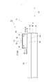
図1は、一実施形態に係る半導体装置用のパッケージ1Aの平面図である。図2は、図1のII-II線に沿った断面を模式的に示す図である。図3は、図1のIII-III線に沿った断面を模式的に示す図である。図1~図3に示すように、本実施形態のパッケージ1Aは、ベース3、側壁4A、2つの入力リード5、2つの出力リード6、接合材7~10、導電層11及び12、複数のビア13、並びに複数のビア14を備える。
FIG. 1 is a plan view of a
ベース3は、金属製の平坦な主面3aを有する板状の部材である。ベース3は、例えば銅、銅とモリブデンの合金、銅とタングステンの合金、あるいは、銅板、モリブデン板、タングステン板、銅とモリブデンの合金板、銅とタングステンの合金板による積層材から成る。図に示す例では、ベース3は、2枚の銅板31、33の間にモリブデン板32が挟まれた構造を有する。ベース3の基材の表面には、ニッケルクロム(ニクロム)-金、ニッケル-金、ニッケル-パラジウム-金、銀若しくはニッケル、又は、ニッケル-パラジウム等のメッキが施されている。金、銀及びパラジウムがメッキ材であり、NiCr及びNi等がシード材である。メッキ材のみの場合よりもメッキ材及びシード材を含む場合の方が密着性を高めることができる。ベース3の厚さは、例えば、0.5~1.5mmである。ベース3の平面形状は、例えば長方形状である。
The
側壁4Aは、誘電体としてのセラミックからなる略長方形状の枠状の部材である。図1に示すように、側壁4Aは、ベース3の主面3aに沿う方向D1において互いに対向する一対の部分41,42と、方向D1と交差(例えば直交)する方向D2において互いに対向する一対の部分43,44とを有する。部分41,42は方向D2に沿って互いに平行に延在しており、部分43,44は方向D2に沿って互いに平行に延在している。以下の説明において、部分41を入力側の側壁部分、部分42を出力側の側壁部分と称することがある。延在方向に垂直な各部分41~44の断面は長方形状または正方形状である。主面3aの法線方向における側壁4Aの高さは、例えば0.5~1.0mmである。
The
図2及び図3に示すように、側壁4Aは、ベース3の主面3aと対向する平坦な底面4aと、底面4aとは反対側の上面4bとを有する。底面4a及び上面4bの全面には、タングステン(W)を成膜したのちにニッケル(Ni)のメッキが施されている。図2に示すように、部分41の底面4aは、接合材7を介してベース3の主面3aに接合されている。言い換えると、接合材7は、部分41の底面4aとベース3の主面3aとを互いに接合している。また、図3に示すように、部分42の底面4aは、接合材9を介してベース3の主面3aに接合されている。言い換えると、接合材9は、部分42の底面4aとベース3の主面3aとを互いに接合している。これらの接合材7,9は銀(Ag)を含む。Agを含む接合材としては、例えば銀ロウや他の銀系接合材が挙げられる。一実施例では、接合材7,9は銀ロウである。
As shown in FIGS. 2 and 3, the
入力リード5及び出力リード6は、金属製の板状の部材であって、一例では銅、銅合金、または鉄合金の金属薄板である。入力リード5は、その方向D1における一端部が、側壁4Aの部分41における上面4bと対向している。入力リード5は、側壁4Aの部分41によって、ベース3の主面3aに対して絶縁されている。図2に示すように、入力リード5の一端部は、接合材8を介して部分41の上面4bに接合されている。言い換えると、接合材8は、部分41の上面4bと入力リード5の一端部とを互いに接合している。また、出力リード6は、その方向D1における一端部が、側壁4Aの部分42における上面4bと対向している。出力リード6は、側壁4Aの部分42によって、ベース3の主面3aに対して絶縁されている。図3に示すように、出力リード6の一端部は、接合材10を介して部分42の上面4bに接合されている。言い換えると、接合材10は、部分42の上面4bと出力リード6の一端部とを互いに接合している。これらの接合材8,10もまた、銀(Ag)を含む。一実施例では、接合材8,10は銀ロウである。
The
図2に示すように、導電層11は、側壁4Aの部分41に埋め込まれた導電性材料からなる層であって、底面4aと上面4bとの間に設けられ、側壁4Aの底面4aに沿って延在している。本実施形態の導電層11は、部分41を構成する2つの誘電体層に挟まれている。導電層11は、部分41において、少なくとも主面3aの法線方向(すなわちベース3の厚み方向)から見て入力リード5と重なる位置に設けられている。導電層11は、接合材7と電気的に接続されている。本実施形態では、導電層11と接合材7との電気的な接続を、導電層11と接合材7との間の側壁4Aを貫通する導電性のビア13が行う。但し、導電層11と接合材7との電気的な接続方式はこれに限られない。方向D1における導電層11の一端は、側壁4Aの内側面4cに達しており、内側面4cから露出している。方向D1における導電層11の他端は、側壁4Aの外側面4dに達しており、外側面4dから露出している。
As shown in FIG. 2, the
側壁4Aの接合材7に接合される面(すなわち底面4a)と導電層11との距離h1は、側壁4Aの接合材7に接合される面とは反対側の面(すなわち上面4b)と導電層11との距離h2よりも短い。言い換えると、側壁4Aの高さ方向において、導電層11は底面4a寄りに配置されている。一例では、h1とh2との比(h1/h2)は1/4である。側壁4Aの厚さが0.5mmである場合、距離h1は0.1mmであり、距離h2は0.4mmである。
The distance h1 between the surface of the
図3に示すように、導電層12は、側壁4Aの部分42に埋め込まれた導電性材料からなる層であって、底面4aと上面4bとの間に設けられ、側壁4Aの上面4bに沿って延在している。本実施形態の導電層12は、部分42を構成する2つの誘電体層に挟まれている。導電層12は、部分42において、少なくとも主面3aの法線方向から見て出力リード6と重なる位置に設けられている。導電層12は、接合材10と電気的に接続されている。本実施形態では、導電層12と接合材10との電気的な接続を、導電層12と接合材10との間の側壁4Aを貫通する導電性のビア14が行う。但し、導電層12と接合材10との電気的な接続方式はこれに限られない。方向D1における導電層12の一端は、側壁4Aの内側面4cに達しており、内側面4cから露出している。方向D1における導電層12の他端は、側壁4Aの外側面4dに達しており、外側面4dから露出している。
As shown in FIG. 3,
側壁4Aの接合材10に接合される面(すなわち上面4b)と導電層12との距離h3は、側壁4Aの接合材10に接合される面とは反対側の面(すなわち底面4a)と導電層12との距離h4よりも短い。言い換えると、側壁4Aの高さ方向において、導電層12は上面4b寄りに配置されている。一例では、h3とh4との比(h3/h4)は1/4である。側壁4Aの厚さが0.5mmである場合、距離h3は0.1mmであり、距離h4は0.4mmである。
The distance h3 between the surface of the
導電層11,12は、銀(Ag)を含まない材料からなり、例えばAgを含まない金属材料からなる。一例では、導電層11,12は、タングステン(W)層及びニッケル(Ni)層を含む積層構造を有する。具体的には、上層側の側壁4Aにタングステンを成膜し、これを下地層としてニッケルをメッキ形成する。同様に、下層側の側壁4Aにもタングステンを成膜し、これを下地層としてニッケルをメッキ形成する。そして、上層側及び下層側のニッケル層同士を熱圧着することにより、導電層11,12が形成される。従い、導電層11,12は、タングステン、ニッケル、およびタングステンの3層構造を有する。なお、側壁4Aの内側面4c及び外側面4dから露出した導電層11及び12の端面は、Niメッキにて完全に覆われる。
The
また、ビア13,14は、下層側(または上層側)の側壁4Aに形成されたスルーホール内壁にタングステンを成膜し、これを下地層としてニッケルをメッキ形成してスルーホールを埋め込むことにより形成される。その際、上記の熱圧着後に空孔を残さず、スルーホールを完全に埋め込む。或いは、タングステン粉とセラミック粉を混合して焼成したものを埋め込んでもよい。ビア13,14の径は例えば0.1mmである。
The
図4は、導電層11,12及びビア13,14の配置を示す図であって、導電層11,12及びビア13,14を主面3aの法線方向から見た様子を模式的に示している。理解の容易の為、導電層11,12の存在範囲をハッチングにより示している。図4に示すように、導電層11は入力リード5に対応して2カ所に分かれて設けられ、導電層12は出力リード6に対応して2カ所に分かれて設けられている。各導電層11の方向D2(すなわち入力リード5の幅方向)における長さL1は、入力リード5の一端部の幅W1(図1を参照)と同じか、それよりも僅かに大きい。従って、方向D2における導電層11の存在範囲は、方向D2における入力リード5の一端部の存在範囲を包含する。同様に、各導電層12の方向D2(すなわち出力リード6の幅方向)における長さL2は、出力リード6の一端部の幅W2(図1を参照)と同じか、それよりも僅かに大きい。従って、方向D2における導電層12の存在範囲は、方向D2における出力リード6の一端部の存在範囲を包含する。
FIG. 4 is a diagram showing the arrangement of the
また、本実施形態では、各導電層11に対して、複数のビア13が方向D2に沿って一列に並んで設けられる。同様に、各導電層12に対して、複数のビア14が方向D2に沿って一列に並んで設けられる。ビア13,14は、高周波信号への影響を抑えるために、できるだけ多く設けられることが望ましい。
Further, in the present embodiment, a plurality of
図5は、上述した本実施形態のパッケージ1Aを備える半導体装置100の構成を示す平面図である。図5では、半導体装置100の蓋部を外した状態を示している。この半導体装置100は、パッケージ1Aに加えて、入力整合回路106、半導体ダイ107(半導体素子)、出力整合回路108、及び出力キャパシタ109を備える。入力整合回路106、半導体ダイ107、出力整合回路108、及び出力キャパシタ109は、パッケージ1Aに収容され、ベース3の主面3a上における側壁4Aに囲まれる領域に搭載されている。パッケージ1Aの内部空間が窒素置換された状態で側壁4Aに蓋部が被せられ、ハーメチックシールが施されることにより半導体装置100が使用可能となる。
FIG. 5 is a plan view showing the configuration of a
入力整合回路106、半導体ダイ107、出力整合回路108、及び出力キャパシタ109は、側壁4Aの部分41からこの順で設けられる。半導体ダイ107は、例えば、Si、SiC、GaN、GaAs又はダイヤモンド等の基板を備えるトランジスタであり、当該基板の裏面には金属メッキが施されている。一例では、半導体ダイ107はGaN-HEMTである。入力整合回路106及び出力整合回路108は、例えば、セラミック基板の上面及び下面のそれぞれに電極を設けた平行平板型キャパシタである。
入力整合回路106、半導体ダイ107及び出力整合回路108は、導電性ペーストによりベース3上に固定される。入力整合回路106は半導体ダイ107の入力側に搭載され、出力整合回路108は半導体ダイ107の出力側に搭載される。入力リード5と入力整合回路106の間、入力整合回路106と半導体ダイ107の間、半導体ダイ107と出力整合回路108の間、出力整合回路108と出力キャパシタ109の間、及び出力キャパシタ109と出力リード6の間のそれぞれは、図示しない複数のボンディングワイヤにより電気的に接続されている。
The
図6は、半導体ダイ107の表面を示す図である。図7は、半導体ダイ107の裏面を示す図である。図6及び図7に示すように、半導体ダイ107は、細長く延びる矩形状を成している。半導体ダイ107は、一対の短辺107aと一対の長辺107bによって平面形状を画定している。半導体ダイ107は、基板107c、及び基板107cの裏面に設けられるソース電極107dを備える。また、半導体ダイ107は、基板107cの表面に、長辺107bに沿って並ぶ複数のゲート電極107e及びソースビア107f、活性領域107g、並びにドレイン電極107hを備える。ソース電極107dは、例えば、金メッキが施されており、ソース電極107dの厚さは5μm以上且つ20μm以下である。
FIG. 6 is a diagram showing the surface of the semiconductor die 107. As shown in FIG. FIG. 7 is a diagram showing the back surface of the semiconductor die 107. As shown in FIG. As shown in FIGS. 6 and 7, the semiconductor die 107 has an elongated rectangular shape. The semiconductor die 107 has a planar shape defined by a pair of
ゲート電極107eは、活性領域107gから見てドレイン電極107hの反対側に設けられる。活性領域107gはドレインフィンガ及びソースフィンガを含む。ソースフィンガと裏面ソース電極107dとは、半導体ダイ107を貫通するソースビア107fにより電気的に接続される。ドレインからソースに流せる最大の電流値はゲート幅に比例するため、大出力のトランジスタでは、ゲート幅を大きくするために、多くのドレインフィンガ/ソースフィンガを並列に設ける。これにより、半導体ダイ107は、長辺107bに沿って細長く延びる形状となる。
The
再び図5を参照する。入力整合回路106は、入力リード5と半導体ダイ107の間におけるインピーダンスのマッチングを行う。入力整合回路106の一端は、ボンディングワイヤを介して入力リード5と電気的に接続されている。入力整合回路106の他端は、ボンディングワイヤを介して半導体ダイ107のゲート電極107e(図6を参照)と電気的に接続されている。このように、入力リード5は、パッケージ1A内の配線を介して半導体ダイ107のゲート電極107eと電気的に接続されている。ゲート電極107eにはグランド電位よりも低い負のゲートバイアスが印加されるので、入力リード5の電位は、ベース3の主面3aの電位よりも低くなる。
Refer to FIG. 5 again. The
出力整合回路108は、半導体ダイ107と出力リード6の間においてそのインピーダンスを調整し、出力リード6に現れる高周波信号の所望の出力を、最大効率で付与する。出力整合回路108の一端は、ボンディングワイヤを介して半導体ダイ107のドレイン電極107h(図6を参照)と電気的に接続されている。出力整合回路108の他端は、ボンディングワイヤを介して出力リード6と電気的に接続されている。このように、出力リード6は、パッケージ1A内の配線を介して半導体ダイ107のドレイン電極107hと電気的に接続されている。ドレイン電極107hにはグランド電位よりも高い正のドレインバイアスが印加されるので、出力リード6の電位は、ベース3の主面3aの電位よりも高くなる。
以上の構成を備える本実施形態のパッケージ1A及び半導体装置100によって得られる効果について説明する。図2に示したように、パッケージ1Aは、金属製の主面3aを有するベース3と、主面3aに接合材7を介して接合された底面4aを有する誘電体の側壁4Aと、側壁4Aの上面4bに接合された金属製の入力リード5とを備える。そして、接合材7は銀(Ag)を含み、入力リード5の電位はベース3の主面3aの電位よりも低い。従って、何らの工夫もなければ、図8に示す模式図のように、入力リード5と主面3aとの間に生じる電界に起因してイオンマイグレーションが生じ、側壁4Aの内側面4c上及び外側面4d上において、Agのデンドライトが接合材7から入力リード5に向けて成長してしまう(図8の矢印A1,A2)。このデンドライトによって入力リード5と主面3aとが短絡すると、半導体装置100の故障に繋がる。
Effects obtained by the
近年、GaNやSiC、Ga2O3などを主な半導体材料とするワイドギャップ半導体の開発が盛んであり、実用化されつつある。ワイドギャップ半導体は耐電圧が高いことから、電源電圧を高めて移動度を上げたり、電極間寄生容量を減らしたりすることで半導体の性能が高まる。このため、ワイドギャップ半導体では上記の電界が強くなり、イオンマイグレーションが起き易い。 In recent years, wide-gap semiconductors using GaN, SiC, Ga 2 O 3 and the like as main semiconductor materials have been extensively developed and put to practical use. Since wide-gap semiconductors have a high withstand voltage, the performance of semiconductors can be improved by increasing the power supply voltage to increase the mobility and by reducing the parasitic capacitance between electrodes. For this reason, in wide-gap semiconductors, the above-described electric field becomes strong, and ion migration is likely to occur.
上記の課題を解決するため、本実施形態のパッケージ1Aは、図2に示す導電層11を備えている。前述したように、導電層11は、側壁4Aの底面4aと上面4bとの間において、主面3aの法線方向から見て入力リード5と重なる位置に設けられ、接合材7と電気的に接続され、底面4aに沿って延在するとともに側壁4Aの内側面4c及び外側面4dから露出する。そして、導電層11はAgを含まない。内側面4c及び外側面4dにおいて、このような導電層11が側壁4Aから露出することにより、電界は導電層11と入力リード5との間で主に発生し、導電層11と主面3aとの間において生じる電界は僅かとなる。従って、導電層11と主面3aとの間においてはAgイオンを移動させる力が極めて弱くなるので、内側面4c及び外側面4dにおけるAgのデンドライトの成長を抑制し、ベース3の主面3aと入力リード5との短絡を低減することができる。
In order to solve the above problem, the
また、図3に示したように、出力リード6は側壁4Aの上面4bに接合材10を介して接合されている。そして、接合材10はAgを含み、出力リード6の電位はベース3の主面3aの電位よりも高い。従って、何らの工夫もなければ、出力リード6と主面3aとの間に生じる電界に起因してイオンマイグレーションが生じ、側壁4Aの内側面4c上及び外側面4d上において、Agのデンドライトが接合材10から主面3aに向けて成長してしまう。このデンドライトによって出力リード6と主面3aとが短絡すると、半導体装置100の故障に繋がる。
Also, as shown in FIG. 3, the
この課題を解決するため、本実施形態のパッケージ1Aは、図3に示す導電層12を備えている。前述したように、導電層12は、側壁4Aの底面4aと上面4bとの間において、主面3aの法線方向から見て出力リード6と重なる位置に設けられ、接合材10と電気的に接続され、上面4bに沿って延在するとともに側壁4Aの内側面4c及び外側面4dから露出する。そして、導電層12はAgを含まない。内側面4c及び外側面4dにおいて、このような導電層12が側壁4Aから露出することにより、電界は導電層12と主面3aとの間で主に発生し、導電層12と出力リード6との間において生じる電界は僅かとなる。従って、導電層12と出力リード6との間においてはAgイオンを移動させる力が極めて弱くなるので、内側面4c及び外側面4dにおけるAgのデンドライトの成長を抑制し、ベース3の主面3aと出力リード6との短絡を低減することができる。
In order to solve this problem, the
本実施形態のように、導電層11(12)と接合材7(10)との電気的な接続を、導電層11(12)と接合材7(10)との間の側壁4Aを貫通する導電性のビア13(14)が行ってもよい。この場合、簡易な構成でもって導電層11(12)と接合材7(10)とを電気的に接続することができる。
As in this embodiment, the electrical connection between the conductive layer 11 (12) and the bonding material 7 (10) is made by penetrating the
本実施形態のように、側壁4Aの接合材7(10)に接合される面と導電層11(12)との距離h1(h3)は、側壁4Aの接合材7(10)に接合される面とは反対側の面と導電層11(12)との距離h2(h4)よりも短くてもよい。
As in this embodiment, the distance h1 (h3) between the surface of the
本実施形態のように、側壁4Aはセラミックにより構成され、導電層11,12はタングステン(W)層及びニッケル(Ni)層を含む積層構造を有してもよい。この場合、側壁4Aを構成するセラミック層の間に導電層11,12を容易に形成することができ、且つ側壁4Aの強度も維持することができる。
As in this embodiment, the
(第1変形例)
図9は、上記実施形態の第1変形例に係るパッケージ1Bを示す平面図である。図10は、図9のX-X線に沿った断面を模式的に示す図である。図11は、図9のXI-XI線に沿った断面を模式的に示す図である。図9~図11に示すように、本変形例のパッケージ1Bは、ベース3、側壁4B、2つの入力リード5、2つの出力リード6、接合材7~10、導電層11及び12、複数のビア13、並びに複数のビア14を備える。これらのうち、側壁4B、導電層11及び12を除く他の構成の詳細は、上記実施形態と同様である。
(First modification)
FIG. 9 is a plan view showing a
側壁4Bは、樹脂(例えばPCB(Printed Circuit Board)に通常用いられる紙エポキシ、ガラスエポキシ等)からなる略長方形状の枠状の部材である。上述した側壁4Aと同様に、側壁4Bもまた、ベース3の主面3aに沿う方向D1において互いに対向する一対の部分41,42と、方向D1と交差(例えば直交)する方向D2において互いに対向する一対の部分43,44とを有する。部分41,42は方向D2に沿って互いに平行に延在しており、部分43,44は方向D2に沿って互いに平行に延在している。延在方向に垂直な各部分41~44の断面は長方形状または正方形状である。主面3aの法線方向における側壁4Bの高さは、例えば0.5~1.0mmである。
The
図10及び図11に示すように、側壁4Bは、ベース3の主面3aと対向する平坦な底面4aと、底面4aとは反対側の上面4bとを有する。底面4a及び上面4bの全面には、プリント配線パターン45が形成されている。プリント配線パターン45は、側壁4Bに固着した金属膜(具体的には、Cu膜上にAuまたはNiのメッキを施したもの)である。図10に示すように、部分41の底面4aは、プリント配線パターン45および接合材7を介してベース3の主面3aに接合されている。言い換えると、接合材7は、部分41の底面4aとベース3の主面3aとを互いに接合している。また、図11に示すように、部分42の底面4aは、プリント配線パターン45および接合材9を介してベース3の主面3aに接合されている。言い換えると、接合材9は、部分42の底面4aとベース3の主面3aとを互いに接合している。これらの接合材7,9は、上記実施形態と同様に、銀(Ag)を含む。Agを含む接合材としては、例えば銀ロウや他の銀系接合材が挙げられる。他の銀系接合材としては、例えば、粒径10nm~10μmの銀フィラーを含有するエポキシ接着剤、銀フィラー及び溶剤からなる焼結型ナノ銀ペースト等が挙げられる。いずれも微細な銀フィラーが活性化し、低温で溶融する現象を含み、金(Au)と銀(Ag)との金属的結合となるので、強度及び長期信頼性に優れる。一実施例では、接合材7,9は焼結型ナノ銀ペーストである。
As shown in FIGS. 10 and 11, the
入力リード5は、その方向D1における一端部が、側壁4Bの部分41における上面4bと対向している。入力リード5は、側壁4Bの部分41によって、ベース3の主面3aに対して絶縁されている。図10に示すように、入力リード5の一端部は、接合材8及びプリント配線パターン45を介して、部分41の上面4bに接合されている。言い換えると、接合材8は、部分41の上面4bと入力リード5の一端部とを互いに接合している。また、出力リード6は、その方向D1における一端部が、側壁4Bの部分42における上面4bと対向している。出力リード6は、側壁4Bの部分42によって、ベース3の主面3aに対して絶縁されている。図11に示すように、出力リード6の一端部は、接合材10及びプリント配線パターン45を介して部分42の上面4bに接合されている。言い換えると、接合材10は、部分42の上面4bと出力リード6の一端部とを互いに接合している。これらの接合材8,10もまた、銀(Ag)を含む。一実施例では、接合材8,10は焼結型ナノ銀ペーストである。
One end of the
導電層11及び12は、次の点を除いて、上記実施形態と同様の構成を有する。すなわち、本変形例の導電層11及び12は、Cu層と、Au層またはニッケルNi層とを含む積層構造を有する。具体的には、上層側の側壁4BにCu膜を例えば無電解メッキにより形成し、その表面にAuまたはNiを電界メッキにより形成する。同様に、下層側の側壁4BにもCu膜を形成し、その表面にAuまたはNiを電界メッキにより形成する。そして、上層側及び下層側のAu層またはNi層同士を熱圧着することにより、導電層11,12が形成される。従い、本変形例の導電層11,12は、Cu、Au(またはNi)、およびCuの3層構造を有する。なお、側壁4Bの内側面4c及び外側面4dから露出した導電層11及び12の端面は、AuメッキまたはNiメッキにて完全に覆われる。
The
また、ビア13,14は、下層側(または上層側)の側壁4Bに形成されたスルーホール内に無電解銅メッキを施すことにより形成される。その際、スルーホールを完全に埋め込み、熱圧着後にスルーホール内に空孔を残さない。
The
図12は、本変形例における導電層11,12及びビア13,14の配置を示す図であって、導電層11,12及びビア13,14を主面3aの法線方向から見た様子を模式的に示している。理解の容易の為、導電層11,12の存在範囲をハッチングにより示している。図12に示すように、本変形例における導電層11,12及びビア13,14の配置は、上記実施形態と同様である。
FIG. 12 is a diagram showing the arrangement of the
本変形例では、図10に示す導電層11が側壁4Bに設けられている。上記実施形態と同様に、導電層11は、側壁4Bの底面4aと上面4bとの間において、主面3aの法線方向から見て入力リード5と重なる位置に設けられ、接合材7と電気的に接続され、底面4aに沿って延在するとともに側壁4Bの内側面4c及び外側面4dから露出する。そして、導電層11はAgを含まない。従って、内側面4c及び外側面4dにおけるAgのデンドライトの成長を抑制し、ベース3の主面3aと入力リード5との短絡を低減することができる。
In this modification, the
また、本変形例では、図11に示す導電層12が設けられている。上記実施形態と同様に、導電層12は、側壁4Bの底面4aと上面4bとの間において、主面3aの法線方向から見て出力リード6と重なる位置に設けられ、接合材10と電気的に接続され、上面4bに沿って延在するとともに側壁4Bの内側面4c及び外側面4dから露出する。そして、導電層12はAgを含まない。従って、内側面4c及び外側面4dにおけるAgのデンドライトの成長を抑制し、ベース3の主面3aと出力リード6との短絡を低減することができる。
Moreover, in this modified example, a
(第2変形例)
図13は、上記実施形態の第2変形例に係るパッケージ1Cの入力リード5を含む断面を模式的に示す図である。図14は、パッケージ1Cの出力リード6を含む断面を模式的に示す図である。図15は、本変形例における導電層11,12及びビア13,14の配置を示す図であって、導電層11,12及びビア13,14を主面3aの法線方向から見た様子を模式的に示している。理解の容易の為、導電層11,12の存在範囲をハッチングにより示している。
(Second modification)
FIG. 13 is a diagram schematically showing a cross section including the input leads 5 of the
図13~図15に示すように、本変形例のパッケージ1Cは、ベース3、側壁4B、入力リード5、出力リード6、接合材7~10、導電層11及び12、複数のビア13、並びに複数のビア14を備える。これらのうち、導電層11及び12、複数のビア13、並びに複数のビア14を除く他の構成の詳細は、上記第1変形例と同様である。
As shown in FIGS. 13 to 15, the
図13及び図15に示すように、本変形例の導電層11は、側壁4Bの内側面4c寄りに偏って設けられ内側面4cから露出する第1部分11aと、側壁4Bの外側面4d寄りに偏って設けられ外側面4dから露出する第2部分11bとを含んで構成されている。第1部分11aと第2部分11bとは、底面4aから互いに等しい距離で設けられ、側壁4Bの部分41の延在方向と交差する方向に互いに間隔を空けて並んで配置されている。そして、第1部分11a及び第2部分11bは、部分41の延在方向に並ぶ複数のビア13を介して接合材7と電気的に接続されている。
As shown in FIGS. 13 and 15, the
また、図14に示すように、本変形例の導電層12は、側壁4Bの内側面4c寄りに偏って設けられ内側面4cから露出する第1部分12aと、側壁4Bの外側面4d寄りに偏って設けられ外側面4dから露出する第2部分12bとを含んで構成されている。第1部分12aと第2部分12bとは、底面4aから互いに等しい距離で設けられ、側壁4Bの部分42の延在方向と交差する方向に互いに間隔を空けて並んで配置されている。そして、第1部分12a及び第2部分12bは、部分42の延在方向に並ぶ複数のビア14を介して接合材10と電気的に接続されている。
Further, as shown in FIG. 14, the
前述した実施形態では、入力リード5及び出力リード6と対向する位置にグランド電位の導電層11,12を配置するので、電極間容量が大きくなり、高周波のインピーダンスマッチングに支障をきたす場合がある。そのような場合には、本変形例のように、導電層11,12のうち側壁4Bの内部に位置する部分を除いてもよい。この場合、Agのデンドライトの成長を抑制しつつ、インピーダンスの低下を抑えて、高周波信号の整合を容易にすることができる。
In the above-described embodiment, since the ground potential
(第3変形例)
図16は、上記実施形態の第3変形例に係るパッケージ1Dの入力リード5を含む断面を模式的に示す図である。図17は、パッケージ1Dの出力リード6を含む断面を模式的に示す図である。図18の(a)及び(b)は、本変形例における導電層11,12及びビア13,14の配置を示す図であって、導電層11,12及びビア13,14を主面3aの法線方向から見た様子を模式的に示している。理解の容易の為、導電層11,12の存在範囲をハッチングにより示している。
(Third modification)
FIG. 16 is a diagram schematically showing a cross section including input leads 5 of a
図16、図17、並びに図18の(a)及び(b)に示すように、本変形例のパッケージ1Dは、ベース3、側壁4B、入力リード5、出力リード6、接合材7~10、導電層11及び12、単一(若しくは2つ)のビア13、並びに単一(若しくは2つ)のビア14を備える。これらのうち、導電層11,12、ビア13,14を除く他の構成の詳細は、上記第2変形例と同様である。
As shown in FIGS. 16, 17, and (a) and (b) of FIG. It comprises
本変形例のビア13は、図16に示すように入力リード5の直下には設けられておらず、図18の(a)及び(b)に示すように側壁4Bにおける入力リード5の直下を除く位置に設けられている。具体的に、図18の(a)に示す例では、ビア13は部分41における2つの入力リード5の間の領域に設けられ、図18の(b)に示す例では、ビア13は部分43及び44に設けられている。また、これと同様に、本変形例のビア14は、図17に示すように出力リード6の直下には設けられておらず、図18の(a)及び(b)に示すように側壁4Bにおける出力リード6の直下を除く位置に設けられている。具体的に、図18の(a)に示す例では、ビア14は部分42における2つの出力リード6の間の領域に設けられ、図18の(b)に示す例では、ビア14は部分43及び44に設けられている。
The via 13 of this modification is not provided directly below the
上記実施形態の導電層11,12の電位は、それぞれ接合材7,10の電位から多少の変動があってもよく、厳密に同電位であることは要求されない。従って、本変形例のようにビア13,14はそれぞれ単一(または2つ)であってもよく、また、それぞれ入力リード5および出力リード6から離れて配置されてもよい。このような形態であっても、上記実施形態の効果を十分に奏することができる。
The potentials of the
(第4変形例)
図19は、上記実施形態の第4変形例に係るパッケージ1Eの入力リード5を含む断面を模式的に示す図である。図20は、パッケージ1Eの出力リード6を含む断面を模式的に示す図である。図19及び図20に示すように、本変形例では、ベース3の主面3a上から側壁4Bの内側面4c上にわたって樹脂膜71が設けられている。この樹脂膜71は、半導体ダイ107(図5参照)のマウントに使用される導電性銀ペーストに起因するAgのデンドライトを防止するために、パッケージ1E内部において露出する導電性銀ペーストの全体を覆う膜である。または、この樹脂膜71は、内側面4cの耐湿性向上のために設けられる膜であってもよい。
(Fourth modification)
FIG. 19 is a diagram schematically showing a cross section including input leads 5 of a
この場合、図19に示すように、内側面4cから露出する接合材7の端面は樹脂膜71によって覆われるので、Agのマイグレーションが生じにくくなる。従って、上記第2変形例に示された第1部分11a(図13を参照)を省き、第2部分11bのみとすることができる。また、図20に示すように、接合材10と、主面3aの露出表面との距離が遠くなるので、Agのデンドライトによる出力リード6と主面3aとの短絡を生じにくくすることができる。従って、上記第2変形例に示された第1部分12a(図14を参照)を省き、第2部分12bのみとすることができる。従って、第2変形例と比較して、インピーダンスの低下を更に抑え、高周波信号の整合をより容易にすることができる。
In this case, as shown in FIG. 19, the end face of the
(第5変形例)
図21は、上記実施形態の第5変形例に係るパッケージ1Fの入力リード5を含む断面を模式的に示す図である。本変形例では、入力リード5の端縁5aが、主面3aの法線方向から見て、内側面4cよりも外側に位置する。そして、入力リード5と側壁4Bとを接合する接合材8及びプリント配線パターン45の端縁もまた、入力リード5の端縁5aと揃って内側面4cよりも外側に位置する。従って、本変形例では、側壁4Bの上面4bのうち内側面4c側の部分が露出している。
(Fifth modification)
FIG. 21 is a diagram schematically showing a cross section including the input leads 5 of the
本変形例のように、入力リード5は内側面4cまで延びている必要は無く、内側面4cから後退していてもよい。これにより、入力リード5と導電層11とが対向する面積を減らすことができる。従って、インピーダンスの低下を抑え、高周波信号の整合を容易にすることができる。なお、入力リード5の端縁5aと内側面4cとの距離L3は、例えば0.3mm以下である。
The
本発明による半導体装置用のパッケージおよび半導体装置は、上述した実施形態及び各変形例の例示に限定されるものではなく、他に様々な変形が可能である。例えば、上述した各実施形態及び各変形例を、必要な目的及び効果に応じて互いに組み合わせてもよい。また、上述した実施形態及び各変形例では入力リード5及び出力リード6と重なる領域にのみ導電層11,12が設けられているが、導電層11,12は側壁4A(または4B)の全体に設けられてもよい。また、上記実施形態では半導体素子の例としてGaN-HEMTを例示したが、横方向拡散MOS(LDMOS)やGaAs-FETであってもよく、或いはトランジスタ以外の半導体素子であってもよい。また、第2変形例では導電層11,12が第1部分11a,12a及び第2部分11b,12bの双方を含み、第4変形例では導電層11,12が第2部分11b,12bのみを含んでいるが、導電層11,12は、第1部分11a,12aのみを含んで構成されてもよい。
The semiconductor device package and the semiconductor device according to the present invention are not limited to the above-described embodiments and modifications, and various other modifications are possible. For example, the embodiments and modifications described above may be combined with each other according to the desired purpose and effect. In the above-described embodiment and modifications, the
1A,1B,1C,1D,1E,1F…パッケージ、3…ベース、3a…主面、4A,4B…側壁、4a…底面、4b…上面、4c…内側面、4d…外側面、5…入力リード、5a…端縁、6…出力リード、7,8,9,10…接合材、11,12…導電層、11a,12a…第1部分、11b,12b…第2部分、13,14…ビア、31,33…銅板、32…モリブデン板、41,42,43,44…部分、45…プリント配線パターン、71…樹脂膜、100…半導体装置、106…入力整合回路、107…半導体ダイ、107a…短辺、107b…長辺、107c…基板、107d…ソース電極、107e…ゲート電極、107f…ソースビア、107g…活性領域、107h…ドレイン電極、107d…ソース電極、108…出力整合回路、109…出力キャパシタ、h1,h2,h3,h4,L3…距離、D1,D2…方向、L1,L2…長さ、W1,W2…幅。
1A, 1B, 1C, 1D, 1E,
Claims (12)
前記主面と対向する底面を有する誘電体の側壁と、
銀(Ag)を含み、前記ベースの前記主面と前記側壁の前記底面とを互いに接合する接合材と、
前記側壁の前記底面とは反対側の上面に接合された金属製のリードと、
前記側壁の前記底面と前記上面との間において、前記主面の法線方向から見て前記リードと重なる位置に設けられ、前記接合材と電気的に接続され、前記底面に沿って延在するとともに前記側壁の側面から露出する、銀(Ag)を含まない導電層と、
を備え、
前記導電層と前記接合材との電気的な接続を、前記導電層と前記接合材との間の前記側壁を貫通する導電性のビアが行う、半導体装置用のパッケージ。 a base having a major surface made of metal;
a dielectric sidewall having a bottom surface facing the main surface;
a bonding material that includes silver (Ag) and bonds the main surface of the base and the bottom surface of the side wall to each other;
a metal lead bonded to the top surface of the side wall opposite to the bottom surface;
provided between the bottom surface and the top surface of the side wall at a position overlapping the lead when viewed from the normal direction of the main surface, electrically connected to the bonding material, and extending along the bottom surface; a conductive layer that does not contain silver (Ag) and is exposed from the side surface of the sidewall with
with
A package for a semiconductor device, wherein a conductive via passing through the side wall between the conductive layer and the bonding material electrically connects the conductive layer and the bonding material .
前記主面に接合された底面を有する誘電体の側壁と、
前記側壁の前記底面とは反対側の上面と対向する金属製のリードと、
銀(Ag)を含み、前記リードと前記側壁の前記上面とを互いに接合する接合材と、
前記側壁の前記底面と前記上面との間において、前記主面の法線方向から見て前記リードと重なる位置に設けられ、前記接合材と電気的に接続され、前記上面に沿って延在するとともに前記側壁の側面から露出する、銀(Ag)を含まない導電層と、
を備える、半導体装置用のパッケージ。 a base having a major surface made of metal;
a dielectric sidewall having a bottom surface joined to the major surface;
a metal lead facing the upper surface of the side wall opposite to the bottom surface;
a bonding material that includes silver (Ag) and bonds the leads and the upper surfaces of the sidewalls to each other;
provided between the bottom surface and the top surface of the side wall at a position overlapping the lead when viewed from the normal direction of the main surface, electrically connected to the bonding material, and extending along the top surface; a conductive layer that does not contain silver (Ag) and is exposed from the side surface of the sidewall with
A package for a semiconductor device, comprising:
前記導電層はタングステン(W)層及びニッケル(Ni)層を含む積層構造を有する、請求項1から請求項4のいずれか1項に記載の半導体装置用のパッケージ。 the dielectric is ceramic,
5. The semiconductor device package according to claim 1, wherein said conductive layer has a laminated structure including a tungsten (W) layer and a nickel (Ni) layer.
前記導電層は銅(Cu)層と金(Au)層またはニッケル(Ni)層とを含む積層構造を有する、請求項1から請求項4のいずれか1項に記載の半導体装置用のパッケージ。 the dielectric is a resin,
5. The semiconductor device package according to claim 1, wherein said conductive layer has a laminated structure including a copper (Cu) layer and a gold (Au) layer or a nickel (Ni) layer.
前記パッケージ内に搭載された半導体素子と、
を備え、
前記パッケージは、
金属製の主面を有するベースと、
前記主面と対向する底面を有する誘電体の側壁と、
銀(Ag)を含み、前記ベースの前記主面と前記側壁の前記底面とを互いに接合する接合材と、
前記側壁の前記底面とは反対側の上面に接合された金属製のリードと、
前記側壁の前記底面と前記上面との間において、前記主面の法線方向から見て前記リードと重なる位置に設けられ、前記接合材と電気的に接続され、前記底面に沿って延在するとともに前記側壁の側面から露出する、銀(Ag)を含まない導電層と、
を有し、
前記リードは、前記パッケージ内の配線を介して前記半導体素子と電気的に接続されており、
前記リードの電位は前記ベースの前記主面の電位よりも低い、半導体装置。 a package ;
a semiconductor element mounted in the package;
with
The package includes:
a base having a major surface made of metal;
a dielectric sidewall having a bottom surface facing the main surface;
a bonding material that includes silver (Ag) and bonds the main surface of the base and the bottom surface of the side wall to each other;
a metal lead bonded to the top surface of the side wall opposite to the bottom surface;
provided between the bottom surface and the top surface of the side wall at a position overlapping the lead when viewed from the normal direction of the main surface, electrically connected to the bonding material, and extending along the bottom surface; a conductive layer that does not contain silver (Ag) and is exposed from the side surface of the sidewall with
has
The leads are electrically connected to the semiconductor element via wiring in the package,
A semiconductor device, wherein the potential of the lead is lower than the potential of the main surface of the base.
前記パッケージ内に搭載された半導体素子と、
を備え、
前記リードは、前記パッケージ内の配線を介して前記半導体素子と電気的に接続されており、
前記リードの電位は前記ベースの前記主面の電位よりも高い、半導体装置。 a package according to claim 2;
a semiconductor element mounted in the package;
with
The leads are electrically connected to the semiconductor element via wiring in the package,
A semiconductor device, wherein the potential of the lead is higher than the potential of the main surface of the base.
前記主面と対向する底面を有する誘電体の側壁と、a dielectric sidewall having a bottom surface facing the main surface;
銀(Ag)を含み、前記ベースの前記主面と前記側壁の前記底面とを互いに接合する接合材と、a bonding material that includes silver (Ag) and bonds the main surface of the base and the bottom surface of the side wall to each other;
前記側壁の前記底面とは反対側の上面に接合された金属製のリードと、a metal lead bonded to the top surface of the side wall opposite to the bottom surface;
前記側壁の前記底面と前記上面との間において、前記主面の法線方向から見て前記リードと重なる位置に設けられ、前記接合材と電気的に接続され、前記底面に沿って延在するとともに前記側壁の側面から露出する、銀(Ag)を含まない導電層と、provided between the bottom surface and the top surface of the side wall at a position overlapping the lead when viewed from the normal direction of the main surface, electrically connected to the bonding material, and extending along the bottom surface; a conductive layer that does not contain silver (Ag) and is exposed from the side surface of the sidewall with
を備え、with
前記誘電体は樹脂であり、the dielectric is a resin,
前記導電層は銅(Cu)層と金(Au)層またはニッケル(Ni)層とを含む積層構造を有する、半導体装置用のパッケージ。A package for a semiconductor device, wherein the conductive layer has a laminated structure including a copper (Cu) layer and a gold (Au) layer or a nickel (Ni) layer.
前記主面と対向する底面を有する誘電体の側壁と、a dielectric sidewall having a bottom surface facing the main surface;
銀(Ag)を含み、前記ベースの前記主面と前記側壁の前記底面とを互いに接合する接合材と、a bonding material that includes silver (Ag) and bonds the main surface of the base and the bottom surface of the side wall to each other;
前記側壁の前記底面とは反対側の上面に接合された金属製のリードと、a metal lead bonded to the top surface of the side wall opposite to the bottom surface;
前記側壁の前記底面と前記上面との間において、前記主面の法線方向から見て前記リードと重なる位置に設けられ、前記接合材と電気的に接続され、前記底面に沿って延在するとともに前記側壁の側面から露出する、銀(Ag)を含まない導電層と、provided between the bottom surface and the top surface of the side wall at a position overlapping the lead when viewed from the normal direction of the main surface, electrically connected to the bonding material, and extending along the bottom surface; a conductive layer that does not contain silver (Ag) and is exposed from the side surface of the sidewall with
を備え、with
前記導電層は、前記側壁の内側面寄りに偏って設けられ前記内側面から露出する第1部分と、前記側壁の外側面寄りに偏って設けられ前記外側面から露出する第2部分とのうち少なくとも一方を含み、The conductive layer has a first portion biased toward the inner surface of the sidewall and exposed from the inner surface, and a second portion biased toward the outer surface of the sidewall and exposed from the outer surface. including at least one
前記導電層は前記第2部分のみを含む、半導体装置用のパッケージ。A package for a semiconductor device, wherein the conductive layer includes only the second portion.
Priority Applications (4)
| Application Number | Priority Date | Filing Date | Title |
|---|---|---|---|
| JP2019024289A JP7156641B2 (en) | 2019-02-14 | 2019-02-14 | Packages for semiconductor devices and semiconductor devices |
| CN202080006086.2A CN112997296B (en) | 2019-02-14 | 2020-02-13 | Package for semiconductor device and semiconductor device |
| PCT/JP2020/005628 WO2020166669A1 (en) | 2019-02-14 | 2020-02-13 | Semiconductor device package and semiconductor device |
| US17/292,656 US11581246B2 (en) | 2019-02-14 | 2020-02-13 | Semiconductor device package and semiconductor device |
Applications Claiming Priority (1)
| Application Number | Priority Date | Filing Date | Title |
|---|---|---|---|
| JP2019024289A JP7156641B2 (en) | 2019-02-14 | 2019-02-14 | Packages for semiconductor devices and semiconductor devices |
Publications (2)
| Publication Number | Publication Date |
|---|---|
| JP2020136339A JP2020136339A (en) | 2020-08-31 |
| JP7156641B2 true JP7156641B2 (en) | 2022-10-19 |
Family
ID=72045646
Family Applications (1)
| Application Number | Title | Priority Date | Filing Date |
|---|---|---|---|
| JP2019024289A Active JP7156641B2 (en) | 2019-02-14 | 2019-02-14 | Packages for semiconductor devices and semiconductor devices |
Country Status (4)
| Country | Link |
|---|---|
| US (1) | US11581246B2 (en) |
| JP (1) | JP7156641B2 (en) |
| CN (1) | CN112997296B (en) |
| WO (1) | WO2020166669A1 (en) |
Families Citing this family (1)
| Publication number | Priority date | Publication date | Assignee | Title |
|---|---|---|---|---|
| JP7612968B2 (en) | 2021-09-28 | 2025-01-15 | 住友電工デバイス・イノベーション株式会社 | Semiconductor device, package for semiconductor device, and method for manufacturing package for semiconductor device |
Citations (4)
| Publication number | Priority date | Publication date | Assignee | Title |
|---|---|---|---|---|
| JP2000236034A (en) | 1999-02-16 | 2000-08-29 | Sumitomo Metal Electronics Devices Inc | Package for electronic component |
| JP2005268333A (en) | 2004-03-16 | 2005-09-29 | Mitsubishi Electric Corp | Ceramic package |
| JP2007243145A (en) | 2006-02-07 | 2007-09-20 | Sumitomo Metal Electronics Devices Inc | High heat dissipation electronic component housing package and method of manufacturing same |
| JP2015204426A (en) | 2014-04-16 | 2015-11-16 | Ngkエレクトロデバイス株式会社 | Electronic component accommodation package |
Family Cites Families (10)
| Publication number | Priority date | Publication date | Assignee | Title |
|---|---|---|---|---|
| CA1320006C (en) | 1986-06-02 | 1993-07-06 | Norio Hidaka | Package for integrated circuit |
| JPS63107055A (en) * | 1986-06-02 | 1988-05-12 | Fujitsu Ltd | Package for integrated circuit |
| JPH10163353A (en) | 1996-02-27 | 1998-06-19 | Toshiba Corp | Microwave device package |
| JPH11233697A (en) * | 1998-02-06 | 1999-08-27 | Hitachi Ltd | Semiconductor device and manufacturing method |
| JP3841768B2 (en) * | 2003-05-22 | 2006-11-01 | 新光電気工業株式会社 | Package parts and semiconductor packages |
| US8084299B2 (en) * | 2008-02-01 | 2011-12-27 | Infineon Technologies Ag | Semiconductor device package and method of making a semiconductor device package |
| JP2011165931A (en) | 2010-02-10 | 2011-08-25 | Mitsubishi Electric Corp | High-frequency circuit module |
| JP5897944B2 (en) * | 2012-03-22 | 2016-04-06 | 日本碍子株式会社 | Laminated sintered ceramic interposer and semiconductor package including the laminated sintered ceramic interposer |
| JP5742859B2 (en) * | 2013-01-30 | 2015-07-01 | 日立金属株式会社 | High-speed transmission cable conductor, manufacturing method thereof, and high-speed transmission cable |
| US10366905B2 (en) * | 2015-12-11 | 2019-07-30 | Rohm Co., Ltd. | Semiconductor device |
-
2019
- 2019-02-14 JP JP2019024289A patent/JP7156641B2/en active Active
-
2020
- 2020-02-13 WO PCT/JP2020/005628 patent/WO2020166669A1/en active Application Filing
- 2020-02-13 CN CN202080006086.2A patent/CN112997296B/en active Active
- 2020-02-13 US US17/292,656 patent/US11581246B2/en active Active
Patent Citations (4)
| Publication number | Priority date | Publication date | Assignee | Title |
|---|---|---|---|---|
| JP2000236034A (en) | 1999-02-16 | 2000-08-29 | Sumitomo Metal Electronics Devices Inc | Package for electronic component |
| JP2005268333A (en) | 2004-03-16 | 2005-09-29 | Mitsubishi Electric Corp | Ceramic package |
| JP2007243145A (en) | 2006-02-07 | 2007-09-20 | Sumitomo Metal Electronics Devices Inc | High heat dissipation electronic component housing package and method of manufacturing same |
| JP2015204426A (en) | 2014-04-16 | 2015-11-16 | Ngkエレクトロデバイス株式会社 | Electronic component accommodation package |
Also Published As
| Publication number | Publication date |
|---|---|
| US20220005751A1 (en) | 2022-01-06 |
| JP2020136339A (en) | 2020-08-31 |
| WO2020166669A1 (en) | 2020-08-20 |
| CN112997296A (en) | 2021-06-18 |
| CN112997296B (en) | 2024-06-18 |
| US11581246B2 (en) | 2023-02-14 |
Similar Documents
| Publication | Publication Date | Title |
|---|---|---|
| KR100367936B1 (en) | High frequency integrated circuit device with laminated body | |
| US11955411B2 (en) | Semiconductor device | |
| JP7156641B2 (en) | Packages for semiconductor devices and semiconductor devices | |
| JP7636219B2 (en) | Semiconductor Device | |
| US10985098B2 (en) | Electronic component mounting substrate, electronic device, and electronic module | |
| US11538725B2 (en) | Semiconductor module arrangement | |
| US20200294872A1 (en) | Semiconductor package, semiconductor device, and method for manufacturing semiconductor device | |
| US11502011B2 (en) | Semiconductor module and semiconductor device container | |
| US20230230904A1 (en) | Semiconductor device | |
| CN116487356A (en) | Semiconductor package including chip-substrate compound semiconductor device | |
| US20230146758A1 (en) | Semiconductor device | |
| JP2010034212A (en) | High-frequency ceramic package and method of fabricating the same | |
| CN112805829B (en) | Semiconductor device | |
| EP2722885B1 (en) | Surface mountable power components | |
| JP2025024548A (en) | Package and semiconductor device | |
| US20240292520A1 (en) | Matching circuit board and semiconductor device | |
| US20240170353A1 (en) | Semiconductor device and mounting structure for semiconductor element | |
| WO2024057876A1 (en) | Semiconductor device | |
| JP2000091376A (en) | Electronic circuit device | |
| JP2002324872A (en) | High frequency IC package equipment |
Legal Events
| Date | Code | Title | Description |
|---|---|---|---|
| A625 | Written request for application examination (by other person) |
Free format text: JAPANESE INTERMEDIATE CODE: A625 Effective date: 20211221 |
|
| A131 | Notification of reasons for refusal |
Free format text: JAPANESE INTERMEDIATE CODE: A131 Effective date: 20220628 |
|
| A521 | Request for written amendment filed |
Free format text: JAPANESE INTERMEDIATE CODE: A523 Effective date: 20220823 |
|
| TRDD | Decision of grant or rejection written | ||
| A01 | Written decision to grant a patent or to grant a registration (utility model) |
Free format text: JAPANESE INTERMEDIATE CODE: A01 Effective date: 20220906 |
|
| A61 | First payment of annual fees (during grant procedure) |
Free format text: JAPANESE INTERMEDIATE CODE: A61 Effective date: 20220928 |
|
| R150 | Certificate of patent or registration of utility model |
Ref document number: 7156641 Country of ref document: JP Free format text: JAPANESE INTERMEDIATE CODE: R150 |